Embed Size (px)
Citation preview

World Journal of Condensed Matter Physics, 2011, 1, 37-48 doi:10.4236/wjcmp.2011.12007 Published Online May 2011 (http://www.SciRP.org/journal/wjcmp)
Copyright © 2011 SciRes. WJCMP
37
Dielectric Relaxation in Pure Columbite Phase of SrNb2O6 Ceramic Material: Impedance Analysis Karuna Nidhan Singh, Parmendra Kumar Bajpai*
Department of Pure & Applied Physics, Guru Ghasidas Vishwavidyalaya, Bilaspur, India. Email: [email protected] Received January 5th, 2011; revised March 24th, 2011; accepted March 26th, 2011. ABSTRACT Controlling the heating rate during calcination and cooling rate during sintering, pure columbite like phase of SrNb2O6 is synthesized. By optimizing the sintering temperature, ceramic with density (> 92%) is achieved for material calcined at 1125˚C and sintered at 1200˚C. The ceramic shows orthorhombic structure with lattice parameters a = 11.011 Å, b = 7.7136 Å, c = 5.5969 Å having average grain size ≈ 1.03 μm. The temperature dependent dielectric response shows a peak at temperature 300.9˚C, which shows significant dielectric dispersion towards high temperature side of the peak with almost dispersion free low temperature side; an effect observed in relaxors. Dielectric dispersion in the material is fitted with the Jonscher’s relation. Impedance analysis suggests strongly temperature dependent relaxation. The dielec-tric relaxation is polydispersive and conduction is mainly through grains. The equivalent circuit model for the imped-ance response is proposed and the temperature dependence of circuit elements deduced. The frequency dependent ac conductivity at different temperatures indicated that the conduction is governed through thermally activated processes. AC conduction activation energies are estimated from Arrhenius plots and conduction mechanism is discussed. Keywords: Electro Ceramics, Dielectrics, Microstructure, Sintering Optimization, Dielectric Relaxation
1. Introduction Alkaline earth and transition metal niobate with general formula A2+ Nb2O6 (with A = Mg, Ca, Sr, Ba, Mn, Fe, Co, Ni, Cu, Zn, Cd, and Pb) have been widely studied [1-8]. Most of these compounds stabilize in isomorphic or-thorhombic phase [9,10]. Many of them in columbite phase exhibit, excellent dielectric properties at micro-wave frequencies [11-13]. Moreover, these compounds are generally used as precursor materials for the synthesis of high-Q perovskite Ba(A1/3Nb2/3)O3 [14]. Microwave dielectric properties of the columbite phases are, to a large extent, sensitive to the preparation route [12,15]. However, the synthesis of single phase columbite is often difficult because of the formation of corundum-like (A4Nb2O9) phases [15]. The properties of ceramics are greatly af-fected by the characteristics of the powder such as particle size, morphology, purity and chemical composition [16]. In normal solid state route, compositional homogeneity is generally not achieved. By using chemical methods, e.g. co-precipitation, sol-gel, hydrothermal and colloid emul-sion techniques, one can efficiently control the morphol-ogy and chemical composition of prepared powder [17]. However, the sinterability of the material remains an issue
and often in the chemical synthesis routes, the densifica-tion of materials is not reported that is important for using the materials for device purposes. Further, the earlier stu-dies have mainly concerned about the preparation routes and detailed dielectric behavior; electrical conduction mechanism and contribution of grains and grain bounda-ries in dielectric relaxation are not studied. For any device application, an understanding of these properties is very much required. Therefore in this paper an attempt has been made to control the processing parameter including the oxidation of grain boundaries during cooling from high temperature while sintering the materials. To the best of our knowledge, no such detailed report exists in the literature. We, therefore, report the optimization of pro- cess parameters viz. calcination and sintering in order to prepare the SrNb2O6 in pure columbite phase with good siterability. The dielectric properties and impedance anal-ysis of SrNb2O6 of such phase pure are investigated and reported in the paper.
2. Experimental Procedure 2.1. Sample Preparation SrNb2O6 is synthesized by taking stoichiometric amounts

38 Dielectric Relaxation in Pure Columbite Phase of SrNb2O6 Ceramic Material: Impedance Analysis
Copyright © 2011 SciRes. WJCMP
of SrCO3 (Loba 99.9%), Nb2O5 (Loba 99.5%) using sol-id-state reaction route. The stoichiometric amounts of precursors were wet mixed in acetone for 12 hours. The mixed powders were calcined at 1125˚C for 6 hours in a microprocessor controlled furnace (Superheat, India) with controlled heating profile. Calcined powders were analyzed using X-ray diffraction technique (X-ray dif-fractometer, Rigaku-Miniflex). Fine calcined powders were pressed into cylindrical pellets of 10 mm diameter and 1-2 mm thickness under an isostatic pressure of 100 MPa. Polyvinyl alcohol (PVA) was used as a binder. The pellets were sintered at different temperatures (1150˚C, 1175˚C, 1200˚C, 1225˚C) for 6 hours and cooled down to room temperature with controlled cooling rate.
2.2. Characterization The phase formation of the sintered pellet has been iden-tified using x-ray diffraction analysis with CuKα (λ = 1.54056 Å). For dielectric measurements, the sin-tered samples were electroded with silver paste and heated at 500˚C for 2 hours before measurements were performed. The electrical impedance (Z), capacitance (C) and loss angle (tan) were measured in the temperature range (100 – 400˚C) and at the rate of 2˚C min-1 in the frequency range (100 Hz-1MHz) using a computer con-trolled LCR HI-TESTER (HIOKI-3532-50). Surface morphology of the sample is investigated using surface electron microscopy (SEM).
3. Result and Discussion 3.1. X-ray Diffraction Studies Figure 1(a) depicts the XRD pattern of SrNb2O6 ceramic calcined at 1125˚C. From the observed interplanar spac-ing (dobs) of all XRD peaks, unit cell parameters were obtained using a standard XRD interpretation software POWD. The unit cell was selected for which d = (dobs-dcal) is minimized. All major X-ray reflection peaks observed could be fitted satisfactorily in orthorhombic columbite phase with lattice constants a = 11.011 Å, b = 7.7136 Å, c = 5.5969Å which matches well with reported JCPDS data (JCPDS File No. 28-1243). The powders sintered at different temperatures (1150˚C, 1175˚C, 1200˚C, 1225˚C,) were again subjected to X-ray diffraction anal-ysis as shown in Figure 1(b). Phase pure material is ob-tained for the sample calcined at 1125˚C and sintered at 1200˚C; the experimental density (> 92% of the theoret-ical one) is obtained for sintered material. The estimated density for different sintering temperatures is shown in Table 1. The particle size determined using Scherer for-mula, is estimated ≈ 413Å.
The microstructure of the sintered pellets and distribu-tion of grains over the sample surface were studied by
scanning electron micrographs. The typical SEM micro-graph of SrNb2O6 is shown in Figure 2. Well developed homogeneously distributed and elongated spherical grains are observed. The average grain size (≈ 1.03m) is calculated using linear intercept method.
3.2. Dielectric Study The temperature dependence of both dielectric permittiv-ity and tangent loss (in the inset) are depicted in Figure 3 at different frequencies ( 1 KHz, 5 KHz, 10 KHz, 50 KHz, 100 KHz, and 1 MHz); the values of dielectric constant increases with increase in temperature and a peak evolves at around 300˚C. The peak value of dielec-tric constant as well as that of tangent loss decreases (Figure 3) and the peak shifts towards higher tempera-ture with increase in frequency. The increase in dielectric response with temperature may be due to interfacial po-larization dominating over dipolar polarization. Observed peak also indicates the onset of some additional relaxa-tion mechanism in the material around 300˚C. Dielectric dispersion at higher temperature side of the peak is evi-dent in both components of dielectric permittivity.
The frequency dependence of real (ε’) and imaginary (ε”) part of dielectric constant on a log-log plot at differ-ent temperatures are shown in Figure 4. Up to 200˚C, real part of dielectric constant is higher than its imagi-nary part, and both values decreases with frequency. With further increase in temperature, there is a sudden rise in ε” and it starts with higher value than ε’, inter-secting at 3 kHz at 250˚C; intersecting frequency shift towards higher frequency as temperature increased (4 kHz at 300˚C). Higher values of both the components of dielectric constant, as temperature rises, reveal the effect of space charge polarization and/or conducting ion mo-tion. The relatively higher values of ε” at low frequency, especially at higher temperature, suggests the free charge motion that may be related to ac conductivity relaxation, whereas the large values of ε’ at lower frequencies may be associated with hopping conduction. Moreover, with increase in frequency, the ε’ and ε” terms becomes al-most parallel at higher temperatures. This type of beha-vior is reported in other conducting ion dielectrics [18] and is associated with ion hoping as the dominant me-chanism of dielectric relaxation [19].
The frequency dependence of real (ε’) and imaginary (ε”) part of dielectric constant in the 50-400˚C tempera-ture range on a log-log scale is shown in figures 5(a) and (b), respectively. Both ε’ and ε” show dispersions at low frequencies and gets almost saturated at higher frequen-cies. The dispersions increase with increase in tempera-ture. Such dispersions in both components of complex dielectric constant are observed commonly in ferroelec-trics with appreciable ionic conductivity and are referred

Dielectric Relaxation in Pure Columbite Phase of SrNb2O6 Ceramic Material: Impedance Analysis
Copyright © 2011 SciRes. WJCMP
39
(a)
(b)
Figure 1. (a) X-ray diffraction profile of SrNb2O6 (SN); (b) X-RD pattern of pure phase SrNb2O6 at different sintering tem-perature.

40 Dielectric Relaxation in Pure Columbite Phase of SrNb2O6 Ceramic Material: Impedance Analysis
Copyright © 2011 SciRes. WJCMP
Table 1. Structural parameters for various sintering conditions of SrNb2O6.
Figure 2. SEM micrograph of pure phase SrNb2O6.
Figure 3. Temperature dependence of dielectric constant (ε’). Inset shows temperature dependence of dielectric loss.
Composition Crystal Structure Unit cell parameters in ( Å ) dexptl.gm/c.c dTheo gm/c.c % density
a b c Sample-I Sintered
1150˚C Orthorhombic 11.210 7.6922 5.6254 4.329 5.523 78.38
Sample-II Sintered 1175˚C
Orthorhombic 11.124 7.7102 5.6204 4.5358 5.558 81.60
Sample-III Sintered 1200˚C
Orthorhombic 11.011 7.7136 5.5969 5.2489 5.638 92.60
Sample-IV Sintered 1225˚C
Orthorhombic 11.008 7.7198 5.6126 4.7786 5.619 85.04

Dielectric Relaxation in Pure Columbite Phase of SrNb2O6 Ceramic Material: Impedance Analysis
Copyright © 2011 SciRes. WJCMP
41
Figure 4. Comparison of dispersion in ε’’ and ε’ in the (200˚C - 400˚C) temperature range.
to as low frequency dielectric dispersion (LEDD) [20,21] and are associated with space charge accumulation effect. The complex dielectric constant as a function of the fre-quency ω in accordance with the Jonscher’s power law [22] is
( )( )( ) 10 0* ' '' ( ) n Ta T iε ε ε ε σ ε ω ε ω −
∞= − = + + (1)
where ε∞ is the high frequency value of the dielectric constant, n(T) is the temperature dependent exponent and a(T) determines the strength of the polarizability arising from the universal mechanism in question. The real and imaginary parts of the complex dielectric constant are given as
( )( ) ( )( ) ( )( )102' sin n Tn T a T iπε ε ε ω −
∞= + (2)
( ) ( )( )( )( ) 10 0'' cos
2n Tn T a T iε σ ε ω ε ω −π = +
(3)
where the first term in Equation (2) determines the lattice response and the second term corresponds to charge ca-reer contribution to the dielectric response. Similarly, in Equation (3) the first term reflects the DC conduction contribution and the second term represents the charge career contribution to dielectric loss. At low frequencies, the contribution due to charge career term
( ( )( )( )( )( ) 102sin ( ) n Tn T a T iε ω −π ) dominates and lattice
response part ε∞ can be neglected. Therefore, Equation (2) for constant n yields a straight line with slope (n- 1). At higher frequencies, the charge careers fail to respond to the applied external field and the dielectric constant is mainly due to lattice contribution. This may account for the observed frequency dependence of dielectric constant; a linear decrease with frequency in low frequency region and frequency dependent plateau region at high frequen-cies. With increasing temperature, the range of frequen-cies in which charge career contribution dominates in-crease showing that charges have sufficient energy to overcome the barrier and get released. A non-linear fit-ting using Equations (2) and (3) give the values of para-meters n (T), and a (T), as depicted in Figure 5(c) at dif-ferent temperatures. At low temperatures, n is close to 1, showing Debye type relaxation. With increase in temper-ature, its value decreases showing increase in interaction and distributed relaxation at higher temperatures. The a(T) value increase slowly with temperature showing the strength of polarizability increasing. Frequency disper-sion of ε” gives two slopes, -1 in the low frequency re-gion and (n-1) in the high frequency region. With in-creasing temperature, the frequency range with slope -1(DC conduction) increases and at higher temperatures
2.5 3.0 3.5 4.0 4.5 5.0 5.5 6.0 6.5 7.0
01020304050607080
2.5 3.0 3.5 4.0 4.5 5.0 5.5 6.0 6.5 7.0
0
1000
2000
3000
4000
2.5 3.0 3.5 4.0 4.5 5.0 5.5 6.0 6.5 7.0
0
15000
30000
45000
60000
75000
2.5 3.0 3.5 4.0 4.5 5.0 5.5 6.0 6.5 7.0
0
1000
2000
3000
4000
5000
Die
lect
ric C
onst
ant
log(ω)
ε' at 2000C ε"
Die
lect
ric C
onst
ant
log(ω)
ε' at 2500C ε"
Dile
ctric
Con
stan
t
log(ω)
ε' at 3000C ε"
Die
lect
ric C
onst
ant
log(ω)
ε' at 3500C ε"
200˚C 250˚C
300˚C 350˚C

Dielectric Relaxation in Pure Columbite Phase of SrNb2O6 Ceramic Material: Impedance Analysis
Copyright © 2011 SciRes. WJCMP
42
(b)
(c)
Figure 5. (a) Frequency dependence of real (ε’) part of dielectric constant in the (50-400˚C) temperature range on a log-log scale. (b) Frequency dependence of imaginary (ε”) part of dielectric constant in the (50-400˚C) temperature range on a log- log scale. (c) Temperature dependence of n(T) and a(T).
3 4 5 6 7
1.6
2.0
2.4
2.8
3.2
3.6
log(ε'
)
log(ω)
500C 1000C 1500C 2000C 2500C 3000C 3500C 4000C
2.5 3.0 3.5 4.0 4.5 5.0 5.5 6.0 6.5 7.0
-1.5
0.0
1.5
3.0
4.5
6.0 500C 1000C 1500C 2000C 2500C 3000C 3500C 4000C
log(
ε")
log(ω)
100 150 200 250 300 350 4000.0
0.2
0.4
0.6
0.8
1.0 n(T) a(T)
Temperature(0C)
n(T)
-5.0x10⁻⁷
0.0
5.0x10⁻⁷
1.0x10⁻⁶
1.5x10⁻⁶
a(T)
(a)
(b)
(c)
50˚C 100˚C 150˚C 200˚C 250˚C 300˚C 350˚C 400˚C
50˚C 100˚C 150˚C 200˚C 250˚C 300˚C 350˚C 400˚C
Temperature (˚C)

Dielectric Relaxation in Pure Columbite Phase of SrNb2O6 Ceramic Material: Impedance Analysis
Copyright © 2011 SciRes. WJCMP
43
dc conduction dominates the charge career conduction.
3.3. Impedance Studies The nature of the material response to an applied a.c. field and processes involved is explored by analyzing the a.c. impedance behavior. Impedance spectroscopy may be a better tool to understand the grain and grain boun-dary relaxation process, especially when the contribution of grains is separated from that of grain boundaries. The frequency dependence of the electrical properties of a material can be described in terms of complex impedance Z*, complex admittance Y*, the complex permittivity *, complex electric modulus M*, and the dielectric loss or the dissipation factor tan. They are related to one another [23] as follows; tan " ' M '' M ' Z ' Z '' Y ' Y ''δ ε ε= = = = . In case of single relaxation process, a semicircle is ob-tained for each admittance function when plotted in the complex plane. Spectroscopic techniques present various possibilities insofar as the representation of data is con-cerned. Each representation can be made use of to high-light a particular aspect of the response of a sample. Thus for instance, in as much as Z” vs. frequency plots high-light phenomena with the largest resistance, the M” plots pick out those of the smallest capacitances [23-29]. The sample is sintered at higher temperature (1125˚C), oxy-gen loss may occur. This may lead to the formation of barrier layers at the grain-grain boundary interface thus affecting the impedance of grains and grain boundaries [30].
Figure 6 shows the variation of the imaginary part of the impedance ( ''Z ) as a function of frequency. ''Z plots show broad peaks at different frequencies with asymmetric broadening depending on the temperature of measurement. This would imply that the relaxation is temperature dependent, and there is apparently not a sin-gle relaxation time, and thereby relaxation process in-volved, but different relaxations with their own discrete relaxation times depending on the temperature. As the temperature is increased, in addition to the expected de-crease in magnitude of ''Z , there is a shifts in the peak frequencies towards higher frequency side. Also it is evident that with increasing temperature, there is a broa-dening of the peaks and at temperatures where tempera-ture dependent dielectric response shows peak, the ''Z response is almost flat. As the temperature is increased further, ''Z response increases and then starts decreas-ing associated with peak broadening at increased temper-ature. This implies the spread of relaxation times on both sides of dielectric peak temperatures and the existence of temperature dependent electrical relaxation phenomena. Probably, high temperature triggers grain boundary re-laxation process as is also evident from the asymmetric broadening of the peaks [30].The most probable relaxa-
tion time could be calculated from the loss peak in the ''Z versus frequency plots using the relation τ = RbCb =
1/ωm. From these data, the τ at various temperatures is calculated. Graph between ln(ωm) versus 1/T is shown in inset of Figure 6. The τ value decreases with increasing temperature, indicating that the behavior is typical semi-conductor one. Calculated activation energy for the process is 0.18 eV.
Figure 7 shows M" as a function of frequency at dif-ferent temperatures (inset shows temperature dependence of ωm obtained from M” curve). It is seen that M" exhi-bits a symmetric maximum (M"max). The M"max shifts toward higher frequencies as the temperature is increased. At 300˚C, the electric modulus loss peak crosses the measurement windows and beyond this temperature. At further higher temperature, a more broadened peak ap-pears that shifts towards higher frequencies with in-creasing the temperature. This once again supports two different relaxation processes dominating the response above and below 300˚C. Thus the dielectric response peak observed is associated with switching of relaxation process. Frequency m corresponding to M"max gives the most probable relaxation time τm (ωmτm = 1). Activation energy estimated from modulus data is 0.59 eV below 300˚C and 0.32 eV above this temperature. As the mod-ulus represents the response from the interior of grains, the activation energies for charges (defects) in the bulk are relatively more than for charges within interface re-gion.
The complex impedance plots 'Z vs. ''Z for repre-sentative temperatures is shown in Figure 8. The arc crosses the ''Z axis at lower values with increasing temperatures, showing that the grain resistance decreases with temperature. This could be fitted with series net-work Rs-(R1Q)C1-R2C2, as shown in Figure 8, where Q represents the constant phase element-a capacitor with universal Jonscher’s type capacitance. The series resis-tance Rs in the model is included as the ''Z does not intersect at origin. This may be due to electrode rough-ness and porousness of the material. Inclusion of constant phase element is due to the fact that value of exponent n(T) in Jonscher’s equation decreases up to 0.5 from 1 in dielectric response (Figure 5(c)). The values of parame-ters Rs, R1, C1, R2, C2, Q and n proposed are calculated and plotted in Figures 9 (a) and (b) as a function of temperature. The value of C1 increases slowly with in-crease in temperature whereas the R1 decreases and above the dielectric peak temperature both becomes al-most constant. The behavior could be associated with the grains dominating the conduction process below 300˚C. The series resistance Rs also increases at high tempera-ture and reached maximum at 250˚C, reflecting that the charges trapped at the bulk electrode interface are mig-

44 Dielectric Relaxation in Pure Columbite Phase of SrNb2O6 Ceramic Material: Impedance Analysis
Copyright © 2011 SciRes. WJCMP
rated into the bulk. The most interesting change lies in constant phase element Q that increases with decrease in the value of n. Thus the grain boundaries start trapping free charges that is released from grains at high tempera-tures. The value of R2 and C2 remains almost temperature independent. The resistance associated with grains is much higher than those of grain boundaries below di-electric peak temperature. Therefore the dielectric peak may be associated with resistive grains becoming con-ductive.
3.4. Electrical Conductivity Study
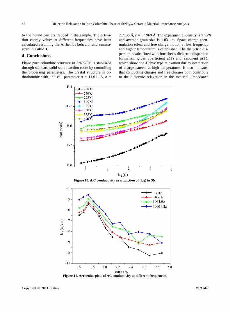
The ac conductivity was calculated from the impedance data using the relation σac = ωε0εr(tanδ) . Figure 10 shows the variation of ac conductivity with frequency at different temperatures. It is clear from the figure that the material at low frequencies exhibits dispersion. Conduc-tivity increases with increase in temperature and frequen-cy. The conductivity could be fitted through the expres-sion σac = σdc + Aωn, known as Jonsher’s law [29],
Figure 6. Frequency dependence of imaginary part of impedance (Z"). Inset shows temperature dependence of m ob- tained from impedance for SN.
Figure 7. Imaginary part of electric modulus (M") as a function of frequencies at representative temperatures for SN.

Dielectric Relaxation in Pure Columbite Phase of SrNb2O6 Ceramic Material: Impedance Analysis
Copyright © 2011 SciRes. WJCMP
45
Figure 8. Complex impedance plots (Z’ vs. Z") at various temperatures along with equivalent circuit fitting for the model as shown in the figure.
Figure 9. (a) Temperature dependence of equivalent circuit parameters (R1, C1, Rs) (b) Temperature dependence of equiva-lent circuit parameters (Q, n, R2C2). where A is a thermally activated quantity and n is the frequency dependent exponent that takes values < 1. The data were fitted using the above relation and the calcu-lated values of σdc, A and n are shown in Table 2. Ac-cording to Jonsher, the origin of the frequency dependent conductivity lies in the relaxation phenomenon arising due to mobile charge carriers. The low frequency disper-sion thus is associated with ac conductivity whereas al-most frequency independent (especially at higher tem-peratures) conductivity at high frequencies corresponds to the dc conductivity of the material. The temperature at
which the grain resistance dominates over grain boun-dary is marked by change in slope of conductivity with frequency. The frequency at which the slope changes is known as hopping frequency, which corresponds to po-laron hopping of charges species [30-32]. As the temper-ature increases, the hopping frequency shifts towards lower side. Temperature dependence of AC conductivity of material is shown in Figure 11. The conductivity of the material is found to increase with increase in temper-ature indicating the NTCR (negative temperature coeffi-cient of resistance) like semiconductors, and it is related
0 50 100 150 200 250 300 350 400 450
0
2000
4000
6000
8000
10000
Serie
s Re
sista
nce(
in Ω
)
Temperature(0C)
Rs0 50 100 150 200 250 300 350 400 450
0
200000
400000
600000
800000
1000000 R1 C1
Gra
in R
esist
ance
(in Ω
)
1.80E-011
2.70E-011
3.60E-011
4.50E-011
5.40E-011 Grain Capacitance(in f)
Temperature (˚C)
46 Dielectric Relaxation in Pure Columbite Phase of SrNb2O6 Ceramic Material: Impedance Analysis
Copyright © 2011 SciRes. WJCMP
to the bound carriers trapped in the sample. The activa-tion energy values at different frequencies have been calculated assuming the Arrhenius behavior and summa-rized in Table 3.
4. Conclusions Phase pure columbite structure in SrNb2O6 is stabilized through standard solid state reaction route by controlling the processing parameters. The crystal structure is or-thorhombic with unit cell parameter a = 11.011 Å, b =
7.7136 Å, c = 5.5969 Å. The experimental density is > 92% and average grain size is 1.03 μm. Space charge accu-mulation effect and free charge motion at low frequency and higher temperature is established. The dielectric dis-persion results fitted with Jonscher’s dielectric dispersion formalism gives coefficient a(T) and exponent n(T), which show non-Debye type relaxation due to interaction of charge careers at high temperatures. It also indicates that conducting charges and free charges both contribute to the dielectric relaxation in the material. Impedance
Figure 10. A.C conductivity as a function of (log) in SN.
Figure 11. Arrhenius plots of AC conductivity at different frequencies.

Dielectric Relaxation in Pure Columbite Phase of SrNb2O6 Ceramic Material: Impedance Analysis
Copyright © 2011 SciRes. WJCMP
47
Table 2. Calculated values of σdc, A and n by expression σac = σdc+ Aωn.
Temperature(˚C) σ dc A n 200 5.4203E-8 2.2404E-8 0.09656 225 2.6683E-9 1.7042E-10 0.50105 250 2.0532E-7 3.2756E-9 0.3982 275 2.7052E-7 1.7647E-7 0.23043
300 2.0637E-6 2.7393E-8 0.43341 325 6.3406E-7 1.1969E-11 0.90399 350 4.4132E-7 5.5385E-12 0.91078 375 7.4112E-7 7.7948E-11 0.72067
400 8.7604E-7 8.409E-11 0.71941
Table 3. Activation energy at different frequencies, calculated by linear fitting of temperature dependence of AC conductivity data.
Frequency in (KHz) Temperature Range
Activation Energy (eV) 75˚C to 150˚C Activation Energy (eV) 175˚C to 325˚C 10 0.054 0.54 100 0.029 0.50
1000 0.14 0.46 spectroscopy is used to model the electrical properties of the material showing the presence of porous material, leakage capacitance and dominating grain response in the material. AC conductivity exhibits dispersion at low fre-quencies and follows Jonscher’s power law. The change in the exponent n in ac conductivity dispersion term (Aωn) reveals the nature of conductivity mechanics. The con-duction mechanism changes from localized hopping to free ion motion with increase in temperature and that the conduction is a thermally activated process.
5. Acknowledgements
PKB would like to acknowledge Department of Science & Technology, Government of India, New Delhi, for the grants received under FIST program and University Grants Commission, New Delhi for Major Research Pro- ject Grant No. F-16/24-2004
REFERENCES [1] K. Brandt and A. Kemi, “X-Ray Studies on ABO4 Com-
pound Rutile Type and AB2O6 Columbite Type,” Mineral. Geol., Vol. 17A, No. 15, 1943.
[2] H. J. Goldschmidt, “An X-Ray Investigation of Systems between Niobium Pentaoxide and Certain Additional Oxides,” Metallurgia, Vol. 62, 1960, pp. 211-218.
[3] F. Laves, G. Bayer and A. Panagos, Schweiz Mineral Petrogr. Mitt., Vol. 43, 1963, p. 217.
[4] H. Brusset, R. Mahe and U. Aung Kyi, “Etude de ni-obates divalents binaires et ternaires a l'etat solide,” Ma-terials Research Bulletin, Vol. 7, No. 10, 1972, pp. 1061- 1073. doi:10.1016/0025-5408(72)90158-4
[5] I. Yaeger, A. H. Morrish and B. M. Wanklyn, “Magneti-zation Studies in Transition-Metal Niobates: I. NiNb2O6,” Physical Review B, Vol. 15, No. 3, 1977, pp. 1465-1476. doi:10.1103/PhysRevB.15.1465
[6] I. Yaeger, I. Maartense and B. M. Wanklyn, “Field-In- duced Magnetic Transitions of CoNb2O6 in the Ordered State,” Solid State Communications, Vol. 21, No. 1, 1977, pp. 93-96. doi:10.1016/0038-1098(77)91485-5
[7] I. Yaeger, A. H. Morrish, B. M. Wanklyn and B. J. Gar-rard, “Magnetization Studies in Transition-Metal Ni-obates. II. FeNb_ 2 O_ 6,” Physical Review B, Vol. 16, 1977, p. 2289. doi:10.1103/PhysRevB.16.2289
[8] K. N. Singh and P. K. Bajpai, “Synthesis, Characteriza-tion and Dielectric Relaxation of Phase Pure Columbite MgNb2O6: Optimization of Calcination and Sinterin,” Physica B, Vol. 405, No.1, January 2010, pp. 303-312.
[9] H. Brusset, M. Gillier-Pandraud and S. D. Voliotis, “Etude de systemes binaires et pseudo-binaires definis entre Nb2O5 et PbO, SrO, BaO,” Materials Research Bulletin, Vol. 6, 1971, p. 5.
[10] R. Roth, “Unit-cell Data of the Lead Niobate, PbNb2O6,”Acta Crystallographica, Vol. 10, No. 6, 1957, p. 437. doi:10.1107/S0365110X57001437
[11] H. J. Lee, K. S. Hong, S. J. Kim and I. T. Kim, “Effect of Vibro-Milling Time on Phase Formation and Particle Size of ZnNbO6 Nano-Powders,” Materials Research Bulletin, Vol. 32, No. 7, 1997, pp. 847-855. doi:10.1016/S0025-5408(97)00034-2
[12] R. C. Pullar, J. D. Breeze and N. Alford, “Characteriza-tion and Microwave Dielectric Properties of M2+ Nb2O6 Ceramics,” Journal of the American Ceramic Society, Vol. 88, No. 9, 2005, pp. 2466-2471. doi:10.1111/j.1551-2916.2005.00458.x

48 Dielectric Relaxation in Pure Columbite Phase of SrNb2O6 Ceramic Material: Impedance Analysis
Copyright © 2011 SciRes. WJCMP
[13] Y. C. Zhang, Z. X. Yue, Z. Gui and L. T. Li, Material Letters, Vol. 57, 2003, pp. 4531-4534.
[14] T. Kolodiazhnyi, A. Petric, A. Belous, O. V’yunov and O. Yanchevskij, “Synthesis and Dielectric Properties of Ba-rium Tantalates and Niobates with Complex Perovskite Structure,” Journal of Materials Research, Vol. 17, No, 12, 2002, pp. 3182-3189. doi:10.1557/JMR.2002.0460
[15] A. Ananta, R. Brydson and N. W. Thomas, “Synthesis, Formation and Characterisation of MgNb2O6 Powder in a Columbite-Like Phase,” Journal of the European Ceram-ic Society, Vol. 19, No. 3, 1999, pp. 355-362. doi:10.1016/S0955-2219(98)00206-4
[16] N. Natarajan, V. Samuel, R. Pasricha, V. Ravi, “A Co-precipitation Technique to Prepare BaNb2O6,” Material Science & Engoneering B, Vol. 117, No. 2, March 2005, pp. 169-171. doi:10.1016/j.mseb.2004.11.009
[17] V. Ravi, “A Coprecipitation Technique to Prepare SrNb2O6,” Material Characterization, Vol. 55, No. 1, Ju-ly 2005, pp. 92-95. doi:10.1016/j.matchar.2005.04.002
[18] K. S. Rao, P. M. Krishan, D. M. Prasad and J. H. Lee, “Influence of Samarium Substitution on Impedance Di-electric and Electromechanical Properties of Pb(1-x)K2xNb2O6,” International Journal of Modern Phys-ics B, Vol. 21, No. 6, 2007, pp. 931-945. doi:10.1142/S0217979207036795
[19] K. S. Rao, D. M. Prasad, P. M. Krishna, B. H. Bindu and K. Suneetha, “Correlation between Low Frequency Di-electric Dispersion (LFDD) and Impedance Relaxation in Ferroelectric Ceramic Pb2KNb4TaO15,” The Journal of Materials Science, Vol. 42, 2007, p. 7363.
[20] L. Zhigao, J. P. Bonnet, J. Ravez and P. Hagenmuller, “Correlation between Low Frequency Dielectric Disper-sion (LFDD) and Impedance Relaxation in Ferroelectric Ceramic Pb2KNb4TaO15,” Solid State Ionics, Vol. 57, No. 3-4, October 1992, pp. 235-244. doi:10.1016/0167-2738(92)90153-G
[21] T. A. Nealon, “Low-Frequency Dielectric Responses in PMN-Type Ceramics,” Ferroelectrics, Vol. 76, 1987, pp. 371-382. doi:10.1080/00150198708016958
[22] A. K. Janscher, “The 'universal'dielectric response,” Na-ture, Vol. 267, 1977, pp. 673-679. doi:10.1038/267673a0
[23] F. A. Kroger and H. J. Vink, “Relations between the Concentrations of Imperfections in Crystalline Solids,” Solid State Physics, Vol. 3, 1956, pp. 307-435. doi:10.1016/S0081-1947(08)60135-6
[24] D. R. Chen and Y. G. Yen, Electro. Elementary Math, Vol. 1, 1982, p. 25.
[25] A. R. West, D. C. Sinclair, N. Hirose, “Characterization of Electrical Materials, Especially Ferroelectrics, by Im-pedance Spectroscopy,” The Journal of Electroceramics. Vol. 1, No.1, 1975, pp. 65-71. doi:10.1023/A:1009950415758
[26] J. Ross Macdonald, “Impedance Spectroscopy: Empha-sizing Solid Materials and Systems,” Wiley Intersicence Publications, 1987.
[27] J. Maier, “The Polarization of Mixed Conducting SOFC Cathodes: Effects of Surface Reaction Coefficient, Ionic Conductivity and Geometry,” The Journal of the Euro-pean Ceramic Society, Vol. 24, No. 6, 2004, pp. 1343- 1347.
[28] J. Maier, Solid State Ionics, Vol. 157, 2003, p. 327. [29] A. K. Jonscher, “The 'universal'dielectric response,” Na-
ture, Vol. 267, 1977, pp. 673-679. [30] D. C. Sinclair and A. R. West, “Impedance and Modulus
Spectroscopy of Semiconducting BaTiO3 Showing Posi-tive Temperature Coefficient of Resistance,” Journal of Applied Physics, Vol. 66, No. 8, 1989, pp. 3850-3857. doi:10.1063/1.344049
[31] I. M. Hodge, M. D. Ingram and Q. A. R. West, “Imped-ance and Modulus Spectroscopy of Polycrystalline Solid Electrolytes,” Journal of Electroanalytical Chemistry, Vol. 74, No. 2, 1976, pp. 125-143. doi:10.1016/S0022-0728(76)80229-X
[32] A.K. Jonscher, “A New Understanding of the Dielectric Relaxation of Solids,” Journal of Materials Science, Vol. 16, No. 8, 1981, pp. 2037-2060. doi:10.1007/BF00542364