Embed Size (px)
Citation preview
Journal of Modern Physics, 2019, 10, 613-623 http://www.scirp.org/journal/jmp
ISSN Online: 2153-120X ISSN Print: 2153-1196
DOI: 10.4236/jmp.2019.106043 May 16, 2019 613 Journal of Modern Physics
Dielectric and Ferroelectric Properties of PZN-4.5PT Nanoparticles Thin Films on Nanostructured Silicon Substrate for Ferrophotovoltaic and Energy Storage Application
Rémi Ndioukane1, Moussa Touré1, Diouma Kobor1, Laurence Motte2, Jeanne Solard3, Laurent Lebrun4
1Laboratoire de Chimie et de Physique des Matériaux (LCPM), University Assane Seck of Ziguinchor, Ziguinchor, Sénégal 2Laboratory for Vascular Translational Science (LVTS), University Paris 13, Paris, France 3Centrale de Proximité en Nanotechnologies de Paris Nord, Paris, France 4Laboratoire Génie Electrique et Ferroélectricité, Institut National des Sciences Appliquées de Lyon, Villeurbanne, France
Abstract The integration of ferroelectric materials as thin films has attracted consider-able attention these last years thanks to their outstanding performances that allow considering new features for the realization of photovoltaic devices. Our study focuses on investigating structural, dielectric and ferroelectric properties of undoped and Mn doped PZN-4.5PT nanoparticles thin films on Silicon substrate. We fabricate very stable PZN-4.5PT nanoparticles thin films deposited on nanostructured silicon substrate with giant relative di-electric permittivity of 2.76 × 10⁴ and 17.7 × 10⁴ for respectively the un-doped and Mn doped thin films. These values are very large compared to those found in single crystals and might be explained by the influence of the gel in which nanoparticles were dispersed. The SEM images show the crys-tallization of new hexagonal phases on the film surface probably coming from interaction between Si and the gel. The hysteresis loops permitted to determine the spontaneous polarization (Ps), remnant polarization (Pr) and coercive field Ec which are equal to 11.73 µC/cm2, 10.20 µC/cm2 and 20 V/cm, respectively for the undoped nanoparticles thin film and 22.22 µC/cm2, 19.32 µC/cm2 and 20 V/cm respectively for the Mn doped one. These values are high and correspond to the best ones found in literature compared to typical ferroelectric thin films.
How to cite this paper: Ndioukane, R., Touré, M., Kobor, D., Motte, L., Solard, J. and Lebrun, L. (2019) Dielectric and Fer-roelectric Properties of PZN-4.5PT Nano-particles Thin Films on Nanostructured Silicon Substrate for Ferrophotovoltaic and Energy Storage Application. Journal of Modern Physics, 10, 613-623. https://doi.org/10.4236/jmp.2019.106043 Received: November 10, 2018 Accepted: May 13, 2019 Published: May 16, 2019 Copyright © 2019 by author(s) and Scientific Research Publishing Inc. This work is licensed under the Creative Commons Attribution International License (CC BY 4.0). http://creativecommons.org/licenses/by/4.0/
Open Access

R. Ndioukane et al.
DOI: 10.4236/jmp.2019.106043 614 Journal of Modern Physics
Keywords PZN-PT, Thin Film, Ferroelectric, Perovskite, Nanoparticles, Gel
1. Introduction
For semiconductor photovoltaic materials, photons with energy higher than the band gap are absorbed to produce electron-hole pairs which are separated by the internalfield in the p-n junction and collected by the electrodes. Consequently, the photo-induced voltage is limited by the energy barrier height at the interface region and usually smaller than the semiconductor band-gap [1]. Therefore, the ferroelectric photovoltaic effect has been attracted a great deal of attention due to its efficient polarization-governed mechanism of charge separation and ability to generate (open circuit voltage) above band-gap voltages [2].
Recently, the discovery of perovskite ferroelectric nanomaterials opened up a great possibility of application for ferroelectric devices. There have been various nanostructures such as nanoparticles, nanorods, and nano-patterned structures using PZT, BaTiO3, and SrTiO3 [3] [4] [5]. Those ferroelectric nanomaterials ex-hibit very different characteristics in its domain dynamics, coercive field and spon-taneous polarization response [6] [7] [8] [9]. Ferroelectric lead compounds having a perovskite structure, such as Pb(Zn1/3Nb2/3)O3 (PZN) [10], Pb(Mg1/3Nb2/3)O3 (PMN) [11], and their solid solutions with PbTiO3 (PT), have been investigated for high performance ultrasonic transducer applications [12] [13] [14] [15] [16]. These solid solutions have excellent piezoelectric and ferroelectric properties in single crystal form compared to the above ferroelectrics. In addition, its high relative dielectric permittivity value could permit to gain a very high open circuit voltage in photovoltaic cells thanks to the charge accumulation process. Then PZN-PT could be one of the promising new materials for such ferrophotovoltaic devices. Indeed, these last years, high levels of papers have been published about PMN-PT and PZN-PT single crystals [17] [18] [19] [20], showing at least fer-roelectric, ferroelastic and piezoelectric properties 10 times higher than those of PZT. However, there is no publication on PZN-PT as thin films for ferrophoto-voltaic effect. We know that the greatest difficulty to use such single crystals on electronic devices is to achieve them in thin layers form because of their incon-gruent melting property. If we fabricate the nanoparticles thin film of such ma-terials without losing ferroelectricity or photovoltaic properties, we can expand the ferroelectric device to various substrates, structures, and nano-scale applica-tions.
In this paper, to integrate them into silicon nanostructures, we realized PZN-4.5PT nanoparticles deposition, already synthesized by the so-called solu-tion flux method [19], as thin film on p-type <100> oriented nanoporous silicon substrate. Surface morphology, dielectric and ferroelectric properties of as depo-sited thin films were investigated.
R. Ndioukane et al.
DOI: 10.4236/jmp.2019.106043 615 Journal of Modern Physics
2. Experimental Procedure 2.1. PZN-PT Nanoparticles Thin Film Fabrication and Surface
Characterization
Undoped and 1% Mn doped PZN-4.5PT grounded powders were dispersed in gel fabricated in the laboratory LCPM in Assane Seck University of Ziguinchor. To obtain a homogeneous film, spinning process was carried out at room tem-perature using a spin coater Midas 1200 D at 3500 rpm with an initial accelera-tion time of 5 seconds and an operating time of 10 min. After 10 min bake in oven at 100˚C, thermal annealing in a K114 type muffle furnace was performed. The heating rate of the furnace is chosen between 10 and 20˚C/min. A 30 - 60 min plateau was carried out at 900˚C for the gel diffusion through the p-type sil-icon (<100> oriented Boron doped monocrystalline silicon with resistivity 5 - 10 Ω.cm and thickness of 600 - 650 μm) nanowires substrate. Cooling at ambient temperature was done naturally. Different samples were fabricated using the two nanopowders and were characterized. Surface morphology of thin films samples were observed using an electron beam lithography system Pioneer Raith model in C(PN)2 (Paris 13 University).
2.2. Dielectric and Ferroelectric Characterization
For dielectric properties characterization, the sample with the deposit thin film was metallized on the both sides with silver paste using the screen-printing me-thod. In order to have good adhesion between the silver and the thin layer, the metallized sample was annealed at 450˚C for 30 min in a thermo scientific model FB1310M-33 oven. For dielectric losses measurements and to calculate the rela-tive dielectric constant (εr), the capacity measurements as function of the tem-perature and the frequency were performed using a LCR meter model LCR-819 from GWINSTEK. The relative dielectric constant was determined using the following formula
0r
CeS
εε
= (1)
where C is the measured capacity, e the thickness, S the metallized surface and ε0 the vacuum permittivity (8.85.10−12 F/m). A modified Sawyer-Tower circuit at room temperature was used to measure the polarization versus the DC field. From polarization-Efield curves, Ec, Pr and Ps were determined.
3. Results and Discussion 3.1. Surface Characterization
Figure 1 shows the SEM images of the different thin layers revealing that the nanoparticles gel is diffused inside the nanowires and covered totally the whole surface. The images of Figure 1(a)-(c) (increasing magnetization) show the complex nature of the undoped nanoparticles thin films randomly distributed. One can find the presence of black zones (Pb is highly reactive with Si at 600˚C

R. Ndioukane et al.
DOI: 10.4236/jmp.2019.106043 616 Journal of Modern Physics
Figure 1. SEM images of (a) normal, (b) zooming on black circle and (c) zooming on gray zone for undoped; (d) normal zone 1, (e) normal zone 2 and (f) zooming on zone for 1% Mn doped PZN-4.5PT nanoparticles thin layers on <100> oriented silicon substrate. to give a hexagonal nano-crystals; on the other hand it is possible that there is a reaction between Pb and the gel giving these nano-crystals), which could be ex-plained by the formation of a new phase and due to the presence of new atoms from the gel containing nanoparticles such as Pb and P that may form new hex-agonal complexes with Si thanks to annealing. In Figure 1(c) top terminals of silicon nanowires could be seen. Figure 1(d) to Figure 1(f) show homogeneous distribution of 1% Mn doped PZN-PT nanoparticles. However, it is interesting to notice that the local black circles are composed by hexagonal shapes nano-crystals (Figure 1(d), Figure 1(e) and the zooming image). Figure 1(f) shows the distribution of the doped nanoparticles on the surface with sizes varying from less than 10 nm to around 200 nm.
3.2. Dielectric and Ferroelectric Characterization
Figure 2 shows the relative dielectric permittivity and dielectric losses as func-tion of temperature. These curves reveal the presence of two transition temper-atures (ferro-ferro and ferro-para). The first transition (TRT = 130˚C) is assigned to a ferroelectric to ferroelectric phase transition which could be from a Rhom-bohedral and hexagonal mixte ferroelectric phase (perovskite nanoparticles and hexagonal nanocrystals) to another ferroelectric phase such as tetragonal or total hexagonal one. Doping did not affect this transition value and the value is closer to the bulk PZN-4.5PT crystals (130˚C [19]). The second peak (around 310˚C) corresponds to the transition from ferroelectric to paraelectric (Tc). According to Figure 2(a) and Figure 2(b), showing permittivity and dielectric losses temper-ature dependence, for undoped and Mn doped PZN-4.5PT nanoparticles thin layers, Tc increased from 180˚C [19] to 310˚C respectively for bulk and for na-noparticles thin layers due to, probably, the gel effect. Relative dielectric permit-tivity (Table 1) values are very high at ambient temperature and 1 kHz (104 to 106 for undoped and 104 to 105 for doped nanoparticles) compared to the bulk one with 103 to 6 × 10³. This remarkable increase in the dielectric permittivity

R. Ndioukane et al.
DOI: 10.4236/jmp.2019.106043 617 Journal of Modern Physics
Table 1. Dielectric and transitions parameters of the undoped and Mn doped nanoparticles thin layers.
Thin films εr (1 kHz) ambient T
tanδe (%) ambient T
TRT (˚C) Tc (˚C) εrmax (at Tc) Ps (µC/cm2) Pr (µC/cm2) Ec (V/cm)
NW-PZN-4.5PT 2.76 × 10⁴ ± 100 6.45 ± 1 130 ± 1 310 ± 1 2.60 × 10⁷ ± 100 11.73 ± 0.1 10.20 ± 0.1 20 ± 1
PZN-4.5PT + 1% Mn 17.7 × 10⁴ ± 100 5.00 ± 1 130 ± 1 305 ± 1 3.00 × 10⁷ ± 100 22.22 ± 0.1 19.32 ± 0.1 20 ± 1
(a)
(b)
Figure 2. Relative dielectric permittivity and dielectric losses versus temperature for (a) undoped and (b) 1% Mn doped PZN-4.5PT nanoparticles thin films deposited on <100> oriented silicon nanowires substrate. could be explained by the new phase from combination of Si-perovskite-gel overgrowth on the silicon surface. The dielectric losses are low compared to other high K materials; their values are equal to 6.45% and 5% respectively for the undoped and Mn doped PZN-4.5PT thin films. These values show that the mechanical factor would be very interesting and high. The results from dielectric

R. Ndioukane et al.
DOI: 10.4236/jmp.2019.106043 618 Journal of Modern Physics
measurements show the potential application of such materials in micro and nanoelectronic devices as a colossal relative dielectric permittivity material.
Figure 3 represents the dielectric permittivity and dielectric losses depen-dence with applied electric field for undoped and Mn doped PZN-4.5PT thin films. From these curves it is clear that the dielectric permittivity value is very colossal in applied electric field conditions. It increases linearly between 15 (εr ≈ 1 × 10⁹) to 25 V/cm reaching to its maximum value (5 × 10⁹) at E ≈ 50 V/cm for undoped film and from 2 × 10⁹ to 9 × 10⁹ for the doped one (Figure 3(a)). Over 60 V/cm, the dielectric permittivity dropped down to its lowest values (εr ≈ 2 × 10⁹ and 7 × 10⁷ respectively for the undoped and Mn doped nanoparticles films). Physically, we supposed that increasing the voltage would permit some defaults and impurities to give enough energy for conduction band. So the increase of the material conductivity would certainly decrease permittivity property.
These results show that this new material could support very large electric field change (40 - 60 V/cm) compared to the other thin films dielectric. However,
(a)
(b)
Figure 3. (a) Relative dielectric permittivity and (b) losses for undoped and 1% Mn doped PZN-4.5PT nanoparticles thin films deposited on <100> oriented silicon nano-wires versus applied electric field.
0
1E+09
2E+09
3E+09
4E+09
5E+09
6E+09
7E+09
8E+09
9E+09
1E+10
0 20 40 60 80 100 120 140 160 180
Ԑr (F
/m)
E (V/cm)
undoped-np doped-np
0
2
4
6
8
10
12
0 20 40 60 80 100 120 140 160 180
D (%
)
E (V/cm)
undoped-np doped-np

R. Ndioukane et al.
DOI: 10.4236/jmp.2019.106043 619 Journal of Modern Physics
over a certain value its performances would decrease. It exists a critical electric field value (around 60 V/cm) corresponding to the maximum dielectric permit-tivity for these materials polarization. The Mn doping did not greatly affect the thin films properties. However, it is clear that it stabilizes the electric field de-pendence (values are more stable compared to undoped). Indeed, one can see in Figure 3(b) that the losses are very stable for applied electric field over 60 V/cm with a value equal around 7% for the doped nanoparticles while it increases suddenly for the undoped one before being stable around 9%.
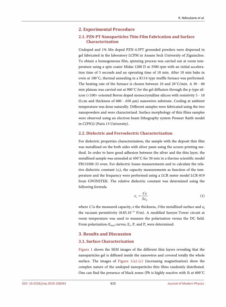
Figure 4 shows the dielectric permittivity and losses as function of frequency with bias on “off” (Figure 4(a) and Figure 4(c)) and with bias on “on” (Figure 4(c) and Figure 4(d)). We note that the bias is remaining at 0 V. The dielectric measurements are carried out as a function of frequency in the range of 100 Hz to 100 kHz to explore relaxation effects. The large dielectric constant for un-doped thin film decreases continuously with an increase in frequency, which is a typical characteristic of any ferroelectric material. Whereas, for the Mn doped sample, the dielectric constant decreases slowly for the further increase in the frequency.
This kind of behavior usually comes from the space charges at low frequen-cies. Along with the improvement in the dielectric constant, an increase in the dielectric loss (Figure 4(c)) is also found for the doped nanoparticles thin film. The dielectric permittivity and losses behaviors in Figure 4(a) and Figure 4(b) (under 0V bias) are totally different to those from Figure 4(a) and Figure 4(c). Indeed, in the latter we notice the presence of negative values (meaning negative capacity) over a certain apparent resonance frequency (around 10 kHz) for both materials. These negative values could come from charge injection and also charge accumulation due to the colossal dielectric permittivity. The relative di-electric permittivity values at high frequency are equal to 1.17 × 10⁴ and 3.9 × 10⁴ for respectively undoped and Mn doped thin films and with bias “off”. These values are in the same range that those determined from dielectric permittivi-ty-temperature curves at 1 kHz (Table 1). The permittivity values with bias on “on” at 0 V are negative and equal to −1.09 × 10⁶ and −2.23 × 10⁶ respectively for
(a)
-2.20E+08
4.78E+09
9.78E+09
1.48E+10
1.98E+10
2.48E+10
2.98E+10
3.48E+10
3.98E+10
0 10 20 30 40 50 60 70 80 90 100
ε r
f (kHz)
undoped Doped
-2.20E+08
4.78E+09
9.78E+09
1.48E+10
1.98E+10
2.48E+10
2.98E+10
3.48E+10
3.98E+10
0 0.05 0.1 0.15 0.2 0.25 0.3 0.35 0.4 0.45 0.5
ε r
f (kHz)
Undoped Doped
R. Ndioukane et al.
DOI: 10.4236/jmp.2019.106043 620 Journal of Modern Physics
(b)
(c)
(d)
Figure 4. Dielectric permittivity versus frequency with (a) 0 V bias “on” and (b) bias “off”; dielectric losses (c) 0 V bias “on” and (d) bias “off” for undoped and Mn doped PZN-4.5PT nanoparticles thin films deposited on <100> oriented silicon nanowires.
undoped and Mn doped samples. The presence of bias since it is equal to 0 V in-creases highly the permittivity values and behavior both for the two films. As ex-plained above, this could be due to charge injection and accumulation. These large relative dielectric values and low dielectric losses make these materials in-teresting candidates for ferrophotovoltaic and energy storage.
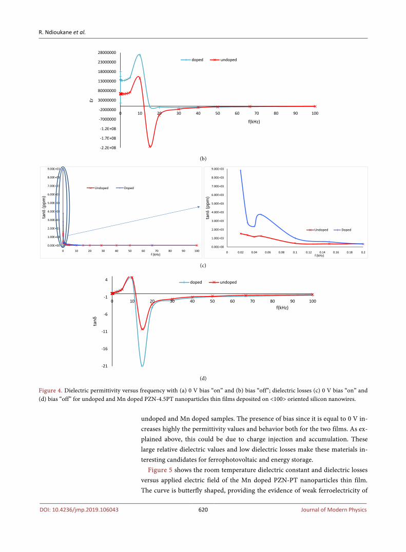
Figure 5 shows the room temperature dielectric constant and dielectric losses versus applied electric field of the Mn doped PZN-PT nanoparticles thin film. The curve is butterfly shaped, providing the evidence of weak ferroelectricity of
-2.2E+08
-1.7E+08
-1.2E+08
-7000000
-2000000
30000000
80000000
13000000
18000000
23000000
28000000
0 10 20 30 40 50 60 70 80 90 100
Ԑr
f(kHz)
doped undoped
0.00E+00
1.00E+03
2.00E+03
3.00E+03
4.00E+03
5.00E+03
6.00E+03
7.00E+03
8.00E+03
9.00E+03
0 10 20 30 40 50 60 70 80 90 100
tanδ
(ppm
)
f (kHz)
Undoped Doped
0.00E+00
1.00E+03
2.00E+03
3.00E+03
4.00E+03
5.00E+03
6.00E+03
7.00E+03
8.00E+03
9.00E+03
0 0.02 0.04 0.06 0.08 0.1 0.12 0.14 0.16 0.18 0.2
tanδ
(ppm
)
f (kHz)
Undoped Doped
-21
-16
-11
-6
-1
4
0 10 20 30 40 50 60 70 80 90 100
tanδ
f(kHz)
doped undoped
R. Ndioukane et al.
DOI: 10.4236/jmp.2019.106043 621 Journal of Modern Physics
(a)
(b)
Figure 5. Completed cycles for (a) relative dielectric permittivity and (b) dielectric losses for 1% Mn doped PZN-4.5PT nanoparticles thin layers deposited on <100> oriented sili-con nanowires substrate. the PZN-PT thin films at room temperature. The tunability ((εmax − εmin)/εmax) of the doped PZN-PT thin films is around 86%. This film showed very high tuna-bility compared to those found in other ferroelectric materials such as the BNT-BT-ST thin films (29% and 35% [21]). This enhancement of dielectric con-stant was attributed to the relatively large hexagonal formed nanocrystals of the thin films due to the reaction between the gel and silicon substrate and also charge accumulation at the thin film and the electrode interface.
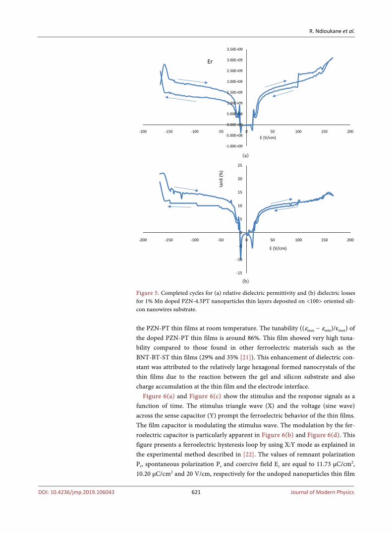
Figure 6(a) and Figure 6(c) show the stimulus and the response signals as a function of time. The stimulus triangle wave (X) and the voltage (sine wave) across the sense capacitor (Y) prompt the ferroelectric behavior of the thin films. The film capacitor is modulating the stimulus wave. The modulation by the fer-roelectric capacitor is particularly apparent in Figure 6(b) and Figure 6(d). This figure presents a ferroelectric hysteresis loop by using X:Y mode as explained in the experimental method described in [22]. The values of remnant polarization Pr, spontaneous polarization Ps and coercive field Ec are equal to 11.73 µC/cm2, 10.20 µC/cm2 and 20 V/cm, respectively for the undoped nanoparticles thin film
-1.00E+09
-5.00E+08
0.00E+00
5.00E+08
1.00E+09
1.50E+09
2.00E+09
2.50E+09
3.00E+09
3.50E+09
-200 -150 -100 -50 0 50 100 150 200E (V/cm)
Ԑr
-15
-10
-5
0
5
10
15
20
25
-200 -150 -100 -50 0 50 100 150 200
tanδ
(%)
E (V/cm)
R. Ndioukane et al.
DOI: 10.4236/jmp.2019.106043 622 Journal of Modern Physics
Figure 6. Modulation of the stimulus triangle wave and response (a) and (c) and their ferroelectric hysteresis loops (b) and (d) for respectively undoped and 1% Mn doped PZN-4.5PT nanoparticles thin layers on <100> oriented silicon nanowires. and 22.22 µC/cm2, 19.32 µC/cm2 and 20 V/cm respectively for the Mn doped thin film. These values are large (high) and correspond to the best ones found in literature compared to typical ferroelectric thin films. One can see that Mn dop-ing increases the polarization values. This is normal compared to the dielectric constant value in room temperature at 1 kHz increasing by doping (Table 1) fa-cilitating charge accumulation and so polarization.
4. Conclusions
In this study, we fabricate with success PZN-4.5PT nanoparticles thin films. Their ferroelectric behavior has been demonstrated, measured and evaluated. We found colossal dielectric constant, which could be explained by the presence of new crystals components probably coming from the reaction between Si and the gel where nanoparticles were dispersed. These results make such thin films very potential candidates for energy storage and for ferrophotovoltaic application.
The determination of the composition of these hexagonal nanocrystals on the film surface and the origin of such colossal relative permittivity would be inves-tigated.
Acknowledgements
This work is supported by Agence Universitaire de la Francophonie (AUF).
Conflicts of Interest
The authors declare no conflicts of interest regarding the publication of this paper.

R. Ndioukane et al.
DOI: 10.4236/jmp.2019.106043 623 Journal of Modern Physics
References [1] Qin, M., Yao, K. and Liang, Y.C. (2008) Applied Physics Letters, 93, Article ID:
122904. https://doi.org/10.1063/1.2990754
[2] Fridkin, V.M. (2001) Crystallography Reports, 46, 654-658. https://doi.org/10.1134/1.1387133
[3] Bernal, A., et al. (2012) Advanced Materials, 24, 1160-1165. https://doi.org/10.1002/adma.201103993
[4] Yuriy, G., Olena, Z. and Anatoliy, G. (2012) Emerging Applications of Ferroelectric Nanoparticles in Materials Technologies, Biology and Medicine. In: Peláiz-Barranco, A., Ed., Advances in Ferroelectrics, IntechOpen, Rijeka Craotia, 475-497.
[5] Joshi, U.A. and Lee, J.S. (2005) Small, 1, 1172-1176. https://doi.org/10.1002/smll.200500055
[6] Lang, X.Y. and Jiang, Q. (2007) Journal of Nanoparticle Research, 9, 595-603. https://doi.org/10.1007/s11051-005-9066-1
[7] Varghese, J., Whatmore, R.W. and Holmes, J.D. (2013) Journal of Materials Chemi-stry C, 1, 2618-2638. https://doi.org/10.1039/c3tc00597f
[8] Michael, T., Trimper, S. and Wesselinowa, J.M. (2006) Physical Review B, 74, Ar-ticle ID: 214113. https://doi.org/10.1103/PhysRevB.74.214113
[9] Basun, S.A., et al. (2011) Physical Review B, 84, Article ID: 024105. https://doi.org/10.1103/PhysRevB.84.024105
[10] Bokov, V. A. and Myl’nikova, I.E. (1960) Soviet Physics, Solid State, 2, 2428.
[11] Smolenskii, G.A., Isupov, V.A., Agranovskaya, A.I. and Popov, S.N. (1961) Soviet Physics, Solid State, 2, 2584.
[12] Nomura, S., Takahashi, T. and Yokomizo, Y. (1969) Journal of the Physical Society of Japan, 27, 262. https://doi.org/10.1143/JPSJ.27.262
[13] Kuwata, J., Uchino, K. and Nomura, S. (1981) Ferroelectrics, 37, 579-582. https://doi.org/10.1080/00150198108223490
[14] Kuwata, J., Uchino, K. and Nomura, S. (1982) Japanese Journal of Applied Physics, 21, 1298. https://doi.org/10.1143/JJAP.21.1298
[15] Shrout, T.R., Change, Z.P., Kim, N. and Markgraf, S. (1990) Ferroelectrics Letters Section, 12, 63-69. https://doi.org/10.1080/07315179008201118
[16] Mulvihill, M.L., Park, S.E., Risch, G., Li, Z., Uchino, K. and Shrout, T.R. (1996) Japanese Journal of Applied Physics, 35, 3984. https://doi.org/10.1143/JJAP.35.3984
[17] Lebrun, L., Zhang, S., Randall, C.A., Shrout, T.R. and Guyomar, D. (2002) Ceramic Transactions, 136, 117.
[18] Benayad, A., Kobor, D., Lebrun, L., Guiffard, B. and Guyomar, D. (2004) Journal of Crystal Growth, 270, 137-144. https://doi.org/10.1016/j.jcrysgro.2004.06.017
[19] Kobor, D. (2005) Synthesis and Characterization of PZN-4.5PT Single Crystals by Flux Method. Thesis, INSA, Lyon.
[20] Prya, S. and Uchino, K. (2002) Journal of Applied Physics, 91, 4515. https://doi.org/10.1063/1.1459101
[21] Li, W., et al. (2015) Ceramics International, 41, S356-S360. https://doi.org/10.1016/j.ceramint.2015.03.178
[22] Kobor, D., et al. (2015) Processing and Application of Ceramics, 9, 107-115. https://doi.org/10.2298/PAC1502107K