Embed Size (px)
Citation preview
978-1-61284-736-8/11/$26.00 ©2011 IEEE 193 27th IEEE SEMI-THERM Symposium
Die Level Thermal Storage for Improved Cooling of Pulsed Devices
Richard W. Bonner III1, Tapan Desai1, Feng Gao2, Xudong Tang1, Tomas Palacios2, Seungha Shin3, Massoud Kaviany3
1Advanced Cooling Technologies, Inc Lancaster, PA
[email protected] 2Massachusetts Institute of Technology
Cambridge, MA 3University of Michigan
Ann Arbor, MI
Abstract In many communications applications semiconductor
devices operate in a pulsed mode, where rapid temperature transients are continuously experienced within the die. We proposed a novel junction-level cooling technology where a metallic phase change material (PCM) was embedded in close proximity to the active transistor channels without interfering with the device’s electrical response. Here we present multiscale simulations that were performed to determine the thermal performance improvement and electrical performance impact under pulsed operating conditions. The modeling effort was focused on Gallium Nitride (GaN) on Silicon (Si) chips with Indium (In) as the PCM. To accurately capture the microscale transient melting process, a hierarchical multiscale model was developed that includes linking of atomistic-level molecular dynamics simulations and macroscale finite element analysis simulations. Macroscale physics, including the melting process, were captured with a transient two-dimensional finite element analysis (FEA) model. The FEA model also includes interfacial and contact resistances between the semiconductor materials and PCM. Non-equilibrium Molecular Dynamic (MD) simulations were performed to estimate the value of the interfacial resistances between the Si substrate and the In PCM, which included a new interatomic potential between In and Si that was developed from experimental scattering results available in the literature. The thermal modeling results indicate 26% more heat can be dissipated through the PCM enhanced transistor while maintain a safe operating temperature. A separate electrical modeling effort showed that the metallic PCM layer did not create appreciable parasitic capacitances as long as the PCM was farther than 1µm from the active channel. The lower, more constant temperatures achieved by this technology can help improve the reliability and performance of future communication devices.
Keywords Gallium Nitride, Junction Level Cooling, Phase Change
Materials, Heat Storage, Molecular Dynamics
Introduction In the last few years, AlGaN/GaN high electron mobility
transistors (HEMTs) have become the preferred option for solid state amplifiers in the 1-40 GHz frequency range [1,2]. With an output power density of more than 40 W/mm (defined as power per unit length of gate) at 4 GHz, these devices offer
10 times higher power density than Si-based electronics, higher efficiency levels, lower cooling requirements and easier impedance matching. The extremely high power densities available in nitride devices create new challenges for heat management and extraction in these devices. Most GaN transistors are grown on Silicon Carbide (SiC) substrates, which have a thermal conductivity 3 times higher than Si. However, this approach is not ideal. SiC substrates are only available on 4” diameters, and are at least 100 times more expensive than Si. Although SiC dissipates heat more effectively than Si, the heat dissipation still limits device performance. In spite of the unprecedented power densities demonstrated in these devices, commercial GaN devices typically operate at much lower power densities (4-6 W/mm) due to the great difficulty in dissipating the generated heat [3,4]. The device junction temperature needs to be kept below 175°C to minimize degradation in the transport properties of the semiconductor and, more importantly, to assure good reliability. Even when operating at the relatively low power densities of 4 W/mm, large heat sinks are required that significantly reduce the system scalability. New approaches to efficiently extract the heat at the device level will significantly improve the performance of nitride transistors.
Concept A micro-scale thermal storage approach was proposed that takes advantage of the transient behavior in communication devices where heat generating pulses on the order of a few milliseconds or even microseconds are typical. The duty cycle is typically between 2% and 10%. The idea is to increase the effective heat capacity of the material near the active channels of the GaN devices by embedding a PCM (material that changes phase between liquid and solid at a given temperature) in close proximity to the active channels. During the heat generating pulses of each duty cycle, the large amount of heat generated in the GaN devices is temporarily stored in the heat of fusion of the PCM as the solid material is melted. During the inactive times, heat is dissipated as the phase change material re-solidifies.
During operation, GaN device temperatures can oscillate between 150°C and 80°C during the rapid transients. The constant thermal cycling and high maximum junction temperatures cause cyclical thermal stresses that lead to reduced reliability. By using PCMs with significantly lower melting points than 150°C, the peak junction temperature can be reduced and the transient temperature profile stabilized.
Bonner, Die Level Thermal Storage for Improved Cooling of .... 27th IEEE SEMI-THERM Symposium
By reducing the peak junction temperature of the GaN devices and maintaining a more constant temperature, reliability will be greatly improved.
We further proposed to use solders with low melting points as the phase change material. Solders are preferred over paraffin wax based PCMs due to their higher thermal conductivity. In52Sn48 (52% Indium, 48% Tin) is the eutectic solder that was targeted in this study due to its advantageous melting point of 118°C. Initial calculations verified the feasibility of the proposed concept. For a GaN device dissipating 100 W/cm2 during peak power over a 10 ms pulse, a layer of approximately 32 µm of In52Sn48 solder would be required to absorb the heat through heat of fusion. This is very reasonable based on current GaN on Si designs. In this effort, the microscale PCM mechanism was modeled to determine the benefits and feasibility of using PCM to minimize peak junction temperatures and maintain temperature stability. Due to the small size of the required PCM components and fast transient nature of the process, macroscale/finite element analysis and atomicscale/ molecular dynamics analysis were required.
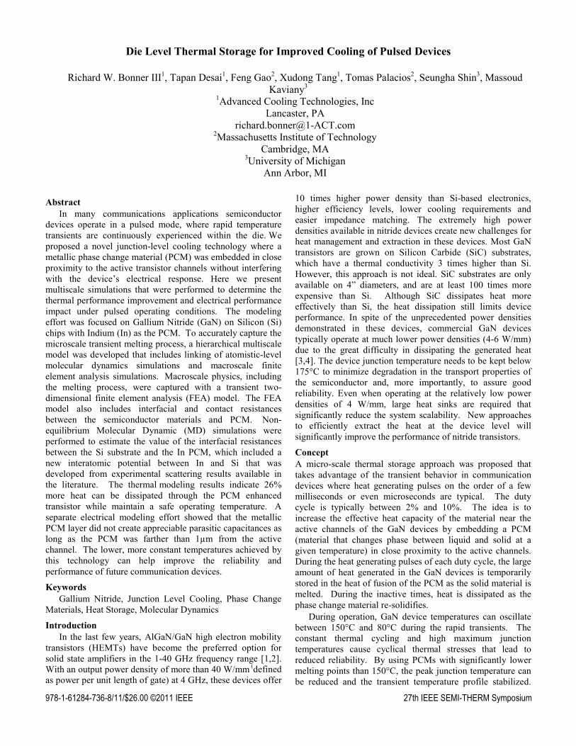
Figure 1 shows the transistor modeled in this study. The transistor consists of an 8µm wide periodic unit cell with two sources, two gates, and one drain. Two localized heat sources (with equal heat fluxes, although typically the heat generation is biased towards the drain) on the GaN surface represent the high heat fluxes generated near the gates. A full scale device consists of many identical unit cells. The whole device is divided into three layers: a 1 µm GaN layer, a silicon 4 µm layer, and 10µm substrate. The grooved structure shown holding the PCM is 2 µm in thickness and 6µm in width, although these dimensions were varied throughout the modeling effort. We studied In52Sn48 as the PCM material, whose heat of fusion is 28.58 kJ/kg. Before the Macroscale Finite Element Analysis (FEA) model could be implemented, the interfacial resistances between the silicon and PCM and between the GaN and Si needed to be estimated. The thermal resistance between GaN and Si was estimated using Diffuse Mismatch Theory [5]. The thermal resistance between Si and the PCM was computed using molecular dynamics as detailed in the Atomistic Scale Modeling section.
Also, we observed that locating a metallic PCM near the junction region might degrade the electrical performance of the device. Analysis was completed using Flex PDE to determine the parasitic capacitance of the metallic PCM as a function of the PCM layer proximity to the junction. Overall, the PCM is able to be located close enough to be thermally effective without degrading performance, as detained in the Parasitic Capacitance Modeling section.
Macroscale Finite-Element Analysis Modeling The modeling domain for the Macroscopic FEA model
was that of Figure 1. A cyclic heat generation boundary condition was applied on the hot spot of the GaN surface as shown in Figure 2. In our analysis, each duty cycle lasted 100 µs. Each cycle consisted of 2 µs of heating time and 98 µs of time in which no heat was generated. A constant heat flux of 5×10⁵ W/cm2 was applied during the heat generation portion of the duty cycle. The heat was generated across the two 0.1 µm length junction regions to simulate heating in the
gate regions. Periodic boundary conditions were applied on the left and right sides of the calculation domain. At the bottom of the unit cell, a convective boundary condition was applied with a fluid temperature of 25°C to approximate the thermal resistance of a heat sink. More details on the numerical techniques used in this analysis can be found in a related work [6].
Figure 1: Thermal model of a GaN Transistor Unit Cell with a PCM groove structure.
Figure 2: Transient heat flux boundary condition.
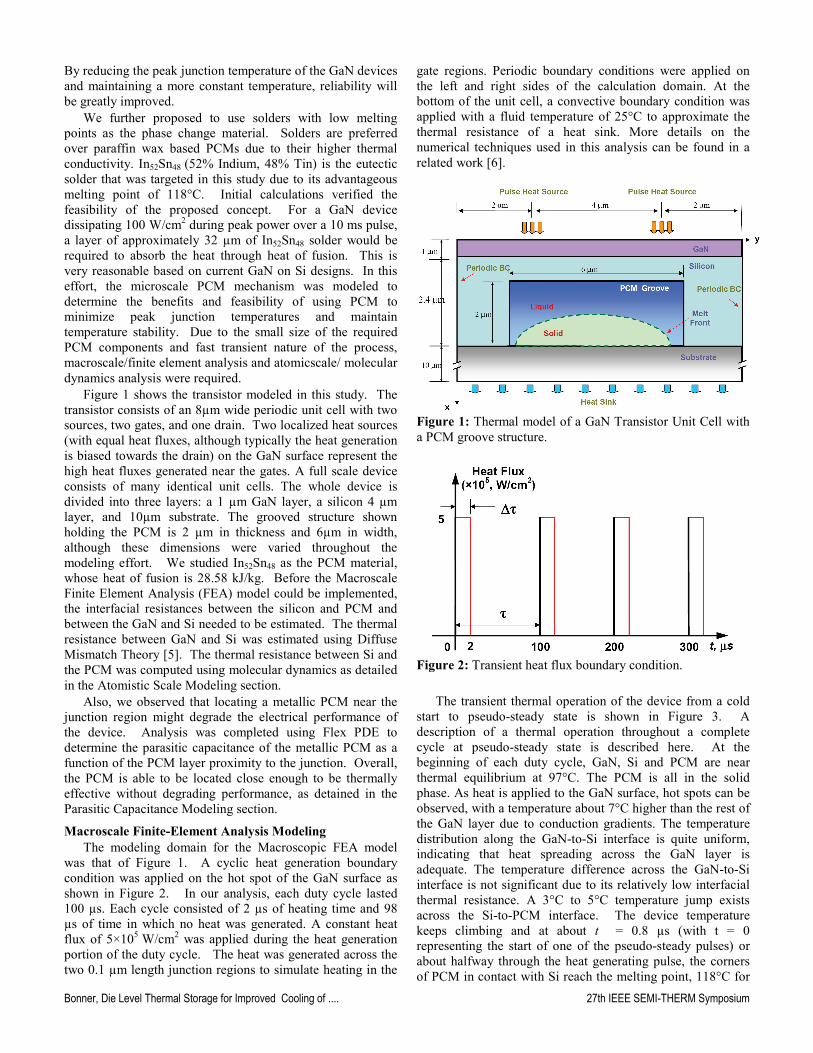
The transient thermal operation of the device from a cold
start to pseudo-steady state is shown in Figure 3. A description of a thermal operation throughout a complete cycle at pseudo-steady state is described here. At the beginning of each duty cycle, GaN, Si and PCM are near thermal equilibrium at 97°C. The PCM is all in the solid phase. As heat is applied to the GaN surface, hot spots can be observed, with a temperature about 7°C higher than the rest of the GaN layer due to conduction gradients. The temperature distribution along the GaN-to-Si interface is quite uniform, indicating that heat spreading across the GaN layer is adequate. The temperature difference across the GaN-to-Si interface is not significant due to its relatively low interfacial thermal resistance. A 3°C to 5°C temperature jump exists across the Si-to-PCM interface. The device temperature keeps climbing and at about t = 0.8 µs (with t = 0 representing the start of one of the pseudo-steady pulses) or about halfway through the heat generating pulse, the corners of PCM in contact with Si reach the melting point, 118°C for
Bonner, Die Level Thermal Storage for Improved Cooling of .... 27th IEEE SEMI-THERM Symposium
In52Sn48. The melt front extends to the entire Si-to-PCM interface to form an arc shaped two-phase interface. As more heat is applied, the melt front propagates towards the heat sink region. During this process, the solid PCM remains at 118°C as conduction gradients are small within the high thermal conductivity PCM. Consequently, it can be seen the hot spot temperature is effectively controlled. At the end of the heat generating pulse, the device temperature reaches a maximum. The hot spot temperature for the PCM case is 135°C, which is 21°C lower than the baseline. Most of PCM in the groove structure is liquid.
Figure 3: Transient thermal result for GaN device under pulsed operating conditions with and without PCM.
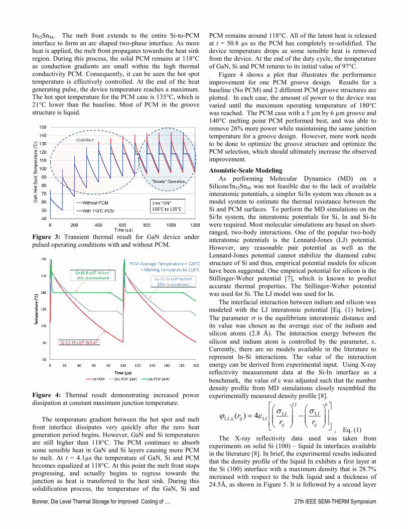
Figure 4: Thermal result demonstrating increased power dissipation at constant maximum junction temperature.
The temperature gradient between the hot spot and melt front interface dissipates very quickly after the zero heat generation period begins. However, GaN and Si temperatures are still higher than 118°C. The PCM continues to absorb some sensible heat in GaN and Si layers causing more PCM to melt. At t = 4.1µs the temperature of GaN, Si and PCM becomes equalized at 118°C. At this point the melt front stops progressing, and actually begins to regress towards the junction as heat is transferred to the heat sink. During this solidification process, the temperature of the GaN, Si and
PCM remains around 118°C. All of the latent heat is released at t = 50.8 µs as the PCM has completely re-solidified. The device temperature drops as some sensible heat is removed from the device. At the end of the duty cycle, the temperature of GaN, Si and PCM returns to its initial value of 97°C.
Figure 4 shows a plot that illustrates the performance improvement for one PCM groove design. Results for a baseline (No PCM) and 2 different PCM groove structures are plotted. In each case, the amount of power to the device was varied until the maximum operating temperature of 180°C was reached. The PCM case with a 5 µm by 6 µm groove and 140°C melting point PCM performed best, and was able to remove 26% more power while maintaining the same junction temperature for a groove design. However, more work needs to be done to optimize the groove structure and optimize the PCM selection, which should ultimately increase the observed improvement.
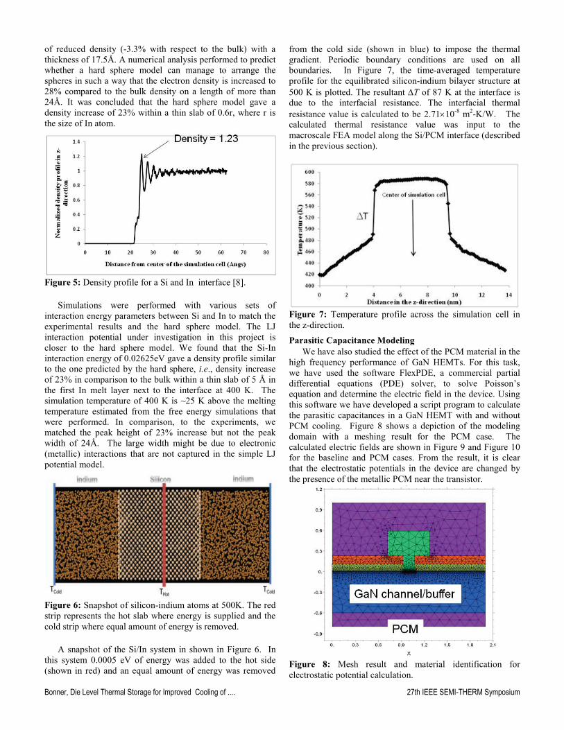
Atomistic-Scale Modeling As performing Molecular Dynamics (MD) on a
Silicon/In52Sn48 was not feasible due to the lack of available interatomic potentials, a simpler Si/In system was chosen as a model system to estimate the thermal resistance between the Si and PCM surfaces. To perform the MD simulations on the Si/In system, the interatomic potentials for Si, In and Si-In were required. Most molecular simulations are based on short-ranged, two-body interactions. One of the popular two-body interatomic potentials is the Lennard-Jones (LJ) potential. However, any reasonable pair potential as well as the Lennard-Jones potential cannot stabilize the diamond cubic structure of Si and thus, empirical potential models for silicon have been suggested. One empirical potential for silicon is the Stillinger-Weber potential [7], which is known to predict accurate thermal properties. The Stillinger-Weber potential was used for Si. The LJ model was used for In.
The interfacial interaction between indium and silicon was modeled with the LJ interatomic potential [Eq. (1) below]. The parameter σ is the equilibrium interatomic distance and its value was chosen as the average size of the indium and silicon atoms (2.8 Å). The interaction energy between the silicon and indium atom is controlled by the parameter, ε. Currently, there are no models available in the literature to represent In-Si interactions. The value of the interaction energy can be derived from experimental input. Using X-ray reflectivity measurement data at the Si-In interface as a benchmark, the value of ε was adjusted such that the number density profile from MD simulations closely resembled the experimentally measured density profile [8].
12 6
LJ LJLJ, LJ( ) 4ij ij
ij ij
rr rσ σϕ ε
= − , Eq. (1)
The X-ray reflectivity data used was taken from experiments on solid Si (100) – liquid In interfaces available in the literature [8]. In brief, the experimental results indicated that the density profile of the liquid In exhibits a first layer at the Si (100) interface with a maximum density that is 28.7% increased with respect to the bulk liquid and a thickness of 24.5Å, as shown in Figure 5. It is followed by a second layer
Bonner, Die Level Thermal Storage for Improved Cooling of .... 27th IEEE SEMI-THERM Symposium
of reduced density (-3.3% with respect to the bulk) with a thickness of 17.5Å. A numerical analysis performed to predict whether a hard sphere model can manage to arrange the spheres in such a way that the electron density is increased to 28% compared to the bulk density on a length of more than 24Å. It was concluded that the hard sphere model gave a density increase of 23% within a thin slab of 0.6r, where r is the size of In atom.
Figure 5: Density profile for a Si and In interface [8].
Simulations were performed with various sets of
interaction energy parameters between Si and In to match the experimental results and the hard sphere model. The LJ interaction potential under investigation in this project is closer to the hard sphere model. We found that the Si-In interaction energy of 0.02625eV gave a density profile similar to the one predicted by the hard sphere, i.e., density increase of 23% in comparison to the bulk within a thin slab of 5 Å in the first In melt layer next to the interface at 400 K. The simulation temperature of 400 K is ~25 K above the melting temperature estimated from the free energy simulations that were performed. In comparison, to the experiments, we matched the peak height of 23% increase but not the peak width of 24Å. The large width might be due to electronic (metallic) interactions that are not captured in the simple LJ potential model.
Figure 6: Snapshot of silicon-indium atoms at 500K. The red strip represents the hot slab where energy is supplied and the cold strip where equal amount of energy is removed.
A snapshot of the Si/In system in shown in Figure 6. In this system 0.0005 eV of energy was added to the hot side (shown in red) and an equal amount of energy was removed
from the cold side (shown in blue) to impose the thermal gradient. Periodic boundary conditions are used on all boundaries. In Figure 7, the time-averaged temperature profile for the equilibrated silicon-indium bilayer structure at 500 K is plotted. The resultant ∆T of 87 K at the interface is due to the interfacial resistance. The interfacial thermal resistance value is calculated to be 2.71×10⁻⁸ m2-K/W. The calculated thermal resistance value was input to the macroscale FEA model along the Si/PCM interface (described in the previous section).
Figure 7: Temperature profile across the simulation cell in the z-direction.
Parasitic Capacitance Modeling We have also studied the effect of the PCM material in the
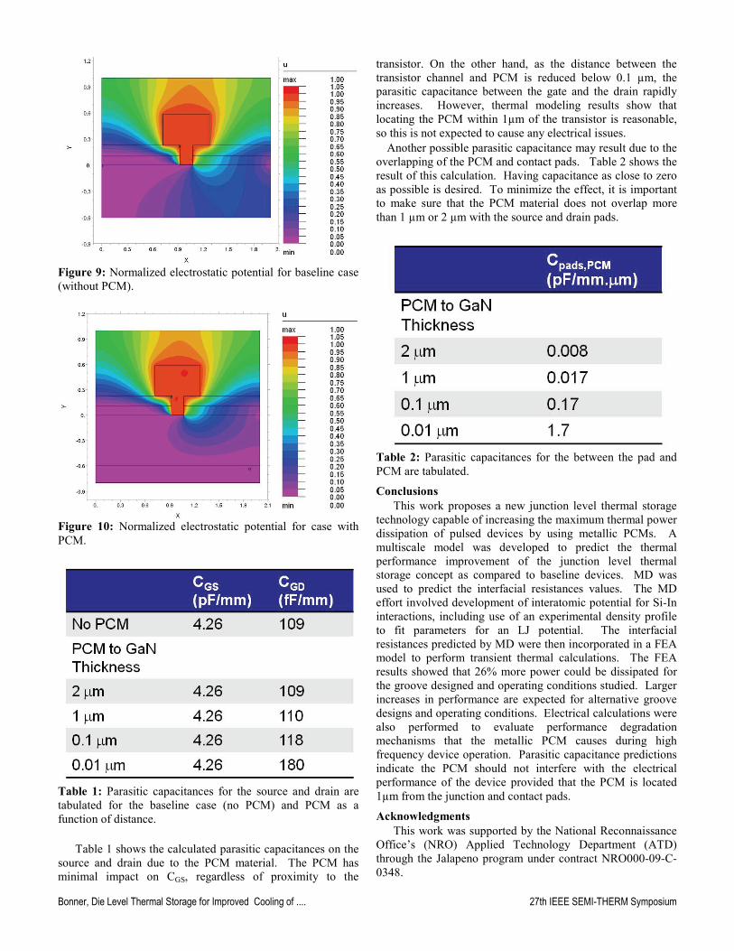
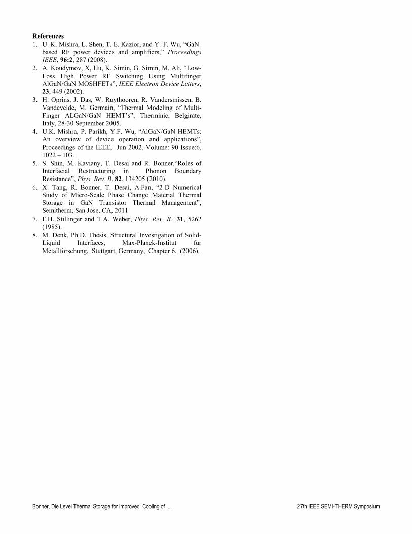
high frequency performance of GaN HEMTs. For this task, we have used the software FlexPDE, a commercial partial differential equations (PDE) solver, to solve Poisson’s equation and determine the electric field in the device. Using this software we have developed a script program to calculate the parasitic capacitances in a GaN HEMT with and without PCM cooling. Figure 8 shows a depiction of the modeling domain with a meshing result for the PCM case. The calculated electric fields are shown in Figure 9 and Figure 10 for the baseline and PCM cases. From the result, it is clear that the electrostatic potentials in the device are changed by the presence of the metallic PCM near the transistor.
Figure 8: Mesh result and material identification for electrostatic potential calculation.
Bonner, Die Level Thermal Storage for Improved Cooling of .... 27th IEEE SEMI-THERM Symposium
Figure 9: Normalized electrostatic potential for baseline case (without PCM).
Figure 10: Normalized electrostatic potential for case with PCM.
Table 1: Parasitic capacitances for the source and drain are tabulated for the baseline case (no PCM) and PCM as a function of distance.
Table 1 shows the calculated parasitic capacitances on the
source and drain due to the PCM material. The PCM has minimal impact on CGS, regardless of proximity to the
transistor. On the other hand, as the distance between the transistor channel and PCM is reduced below 0.1 µm, the parasitic capacitance between the gate and the drain rapidly increases. However, thermal modeling results show that locating the PCM within 1µm of the transistor is reasonable, so this is not expected to cause any electrical issues.
Another possible parasitic capacitance may result due to the overlapping of the PCM and contact pads. Table 2 shows the result of this calculation. Having capacitance as close to zero as possible is desired. To minimize the effect, it is important to make sure that the PCM material does not overlap more than 1 µm or 2 µm with the source and drain pads.
Table 2: Parasitic capacitances for the between the pad and PCM are tabulated.
Conclusions This work proposes a new junction level thermal storage
technology capable of increasing the maximum thermal power dissipation of pulsed devices by using metallic PCMs. A multiscale model was developed to predict the thermal performance improvement of the junction level thermal storage concept as compared to baseline devices. MD was used to predict the interfacial resistances values. The MD effort involved development of interatomic potential for Si-In interactions, including use of an experimental density profile to fit parameters for an LJ potential. The interfacial resistances predicted by MD were then incorporated in a FEA model to perform transient thermal calculations. The FEA results showed that 26% more power could be dissipated for the groove designed and operating conditions studied. Larger increases in performance are expected for alternative groove designs and operating conditions. Electrical calculations were also performed to evaluate performance degradation mechanisms that the metallic PCM causes during high frequency device operation. Parasitic capacitance predictions indicate the PCM should not interfere with the electrical performance of the device provided that the PCM is located 1µm from the junction and contact pads.
Acknowledgments This work was supported by the National Reconnaissance
Office’s (NRO) Applied Technology Department (ATD) through the Jalapeno program under contract NRO000-09-C-0348.
Bonner, Die Level Thermal Storage for Improved Cooling of .... 27th IEEE SEMI-THERM Symposium
References 1. U. K. Mishra, L. Shen, T. E. Kazior, and Y.-F. Wu, “GaN-
based RF power devices and amplifiers,” Proceedings IEEE, 96:2, 287 (2008).
2. A. Koudymov, X, Hu, K. Simin, G. Simin, M. Ali, “Low-Loss High Power RF Switching Using Multifinger AlGaN/GaN MOSHFETs”, IEEE Electron Device Letters, 23, 449 (2002).
3. H. Oprins, J. Das, W. Ruythooren, R. Vandersmissen, B. Vandevelde, M. Germain, “Thermal Modeling of Multi-Finger ALGaN/GaN HEMT’s”, Therminic, Belgirate, Italy, 28-30 September 2005.
4. U.K. Mishra, P. Parikh, Y.F. Wu, “AlGaN/GaN HEMTs: An overview of device operation and applications”, Proceedings of the IEEE, Jun 2002, Volume: 90 Issue:6, 1022 – 103.
5. S. Shin, M. Kaviany, T. Desai and R. Bonner,“Roles of Interfacial Restructuring in Phonon Boundary Resistance”, Phys. Rev. B, 82, 134205 (2010).
6. X. Tang, R. Bonner, T. Desai, A.Fan, “2-D Numerical Study of Micro-Scale Phase Change Material Thermal Storage in GaN Transistor Thermal Management”, Semitherm, San Jose, CA, 2011
7. F.H. Stillinger and T.A. Weber, Phys. Rev. B., 31, 5262 (1985).
8. M. Denk, Ph.D. Thesis, Structural Investigation of Solid-Liquid Interfaces, Max-Planck-Institut für Metallforschung, Stuttgart, Germany, Chapter 6, (2006).