Embed Size (px)
Citation preview
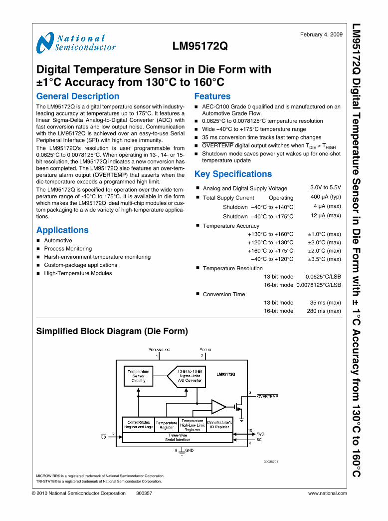
LM95172QFebruary 4, 2009
Digital Temperature Sensor in Die Form with±1°C Accuracy from 130°C to 160°CGeneral DescriptionThe LM95172Q is a digital temperature sensor with industry-leading accuracy at temperatures up to 175°C. It features alinear Sigma-Delta Analog-to-Digital Converter (ADC) withfast conversion rates and low output noise. Communicationwith the LM95172Q is achieved over an easy-to-use SerialPeripheral Interface (SPI) with high noise immunity.
The LM95172Q's resolution is user programmable from0.0625°C to 0.0078125°C. When operating in 13-, 14- or 15-bit resolution, the LM95172Q indicates a new conversion hasbeen completed. The LM95172Q also features an over-tem-perature alarm output (OVERTEMP) that asserts when thedie temperature exceeds a programmed high limit.
The LM95172Q is specified for operation over the wide tem-perature range of -40°C to 175°C. It is available in die formwhich makes the LM95172Q ideal multi-chip modules or cus-tom packaging to a wide variety of high-temperature applica-tions.
Applications■ Automotive
■ Process Monitoring
■ Harsh-environment temperature monitoring
■ Custom-package applications
■ High-Temperature Modules
Features■ AEC-Q100 Grade 0 qualified and is manufactured on an
Automotive Grade Flow.
■ 0.0625°C to 0.0078125°C temperature resolution
■ Wide −40°C to +175°C temperature range
■ 35 ms conversion time tracks fast temp changes
■ OVERTEMP digital output switches when TDIE > THIGH
■ Shutdown mode saves power yet wakes up for one-shottemperature update
Key Specifications
■ Analog and Digital Supply Voltage 3.0V to 5.5V
■ Total Supply Current Operating 400 µA (typ)
Shutdown −40°C to +140°C 4 µA (max)
Shutdown −40°C to +175°C 12 µA (max)
■ Temperature Accuracy
+130°C to +160°C ±1.0°C (max)
+120°C to +130°C ±2.0°C (max)
+160°C to +175°C ±2.0°C (max)
−40°C to +120°C ±3.5°C (max)
■ Temperature Resolution
13-bit mode 0.0625°C/LSB
16-bit mode 0.0078125°C/LSB
■ Conversion Time
13-bit mode 35 ms (max)
16-bit mode 280 ms (max)
Simplified Block Diagram (Die Form)
30035701
MICROWIRE® is a registered trademark of National Semiconductor Corporation.
TRI-STATE® is a registered trademark of National Semiconductor Corporation.
© 2010 National Semiconductor Corporation 300357 www.national.com
LM
95172Q
Dig
ital T
em
pera
ture
Sen
so
r in D
ie F
orm
with
± 1
°C A
ccu
racy fro
m 1
30°C
to 1
60°C
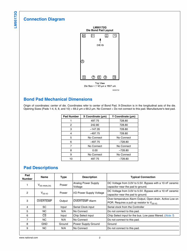
Connection Diagram
LM95172QDie Bond Pad Layout
30035702
Bond Pad Mechanical Dimensions
Origin of coordinates: center of die. Coordinates refer to center of Bond Pad. X-Direction is in the longitudinal axis of the die.Opening Sizes (Pads 1-4, 6, 8, and 10) = 69.2 µm x 69.2 µm. No Connect = Do not connect to this pad. Manufacturer's test pad.
Pad Number X Coordinate (µm) Y Coordinate (µm)
1 497.75 728.80
2 242.80 728.80
3 −147.35 728.80
4 −497.75 728.80
5 No Connect No Connect
6 −497.75 −728.80
7 No Connect No Connect
8 0.00 −728.80
9 No Connect No Connect
10 497.75 −728.80
Pad Descriptions
Pad
NumberName Type Description Typical Connection
1 VDD ANALOG PowerAnalog Power Supply
Voltage
DC Voltage from 3.0V to 5.5V. Bypass with a 10 nF ceramic
capacitor near the pad to ground.
2 VDD IO Power I/O Power Supply VoltageDC Voltage from 3.0V to 5.5V. Bypass with a 10 nF ceramic
capacitor near the pad to ground.
3 OVERTEMP Output OVERTEMP AlarmOver-temperature Alarm Output, Open-drain. Active Low on
POR. Requires a pull-up resistor to VDD IO.
4 SC Input Serial Clock input Serial clock from the Controller
5 NC N/A No Connect Do not connect to this pad.
6 CS Input Chip Select input Chip Select input for the bus. Low pass filtered. (Note 7)
7 NC N/A No Connect Do not connect to this pad.
8 GND Ground Power Supply Ground Ground
9 NC N/A No Connect Do not connect to this pad.
www.national.com 2
LM
95172Q
Pad
NumberName Type Description Typical Connection
10 SI/O Bidirectional Serial I/O Serial I/O Data line to or from the Controller
Backside BACK N/A Substrate connection May be connected to GND connection.
Ordering Information
Order Number NS Package Number Transport Media
LM95172QA2 MDA Die form. No package. 7000 units in 8 mm Surf Tape
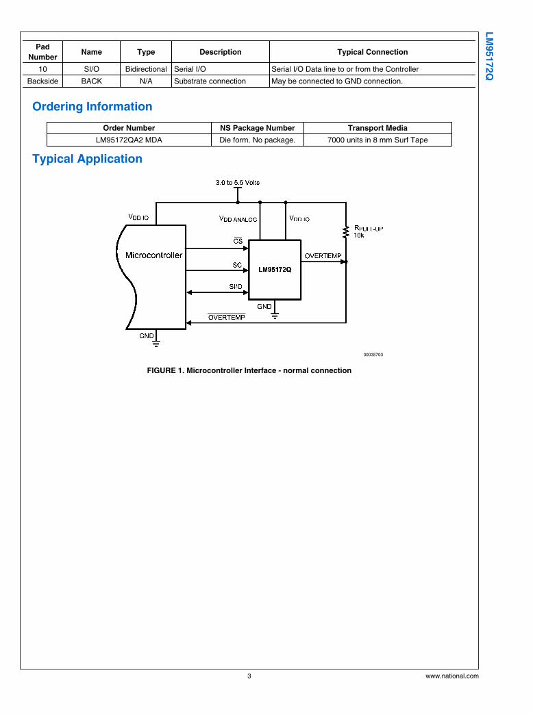
Typical Application
30035703
FIGURE 1. Microcontroller Interface - normal connection
3 www.national.com
LM
95172Q
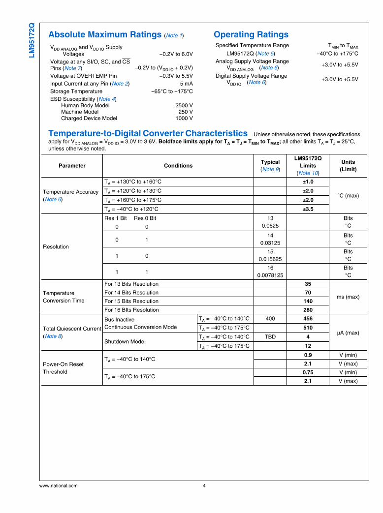
Absolute Maximum Ratings (Note 1)
VDD ANALOG and VDD IO Supply Voltages −0.2V to 6.0V
Voltage at any SI/O, SC, and CSPins (Note 7) −0.2V to (VDD IO + 0.2V)
Voltage at OVERTEMP Pin −0.3V to 5.5V
Input Current at any Pin (Note 2) 5 mA
Storage Temperature −65°C to +175°C
ESD Susceptibility (Note 4) Human Body Model Machine Model Charged Device Model
2500 V250 V
1000 V
Operating RatingsSpecified Temperature Range TMIN to TMAX
LM95172Q (Note 5) −40°C to +175°C
Analog Supply Voltage Range VDD ANALOG (Note 6)
+3.0V to +5.5V
Digital Supply Voltage Range VDD IO (Note 6)
+3.0V to +5.5V
Temperature-to-Digital Converter Characteristics Unless otherwise noted, these specifications
apply for VDD ANALOG = VDD IO = 3.0V to 3.6V. Boldface limits apply for TA = TJ = TMIN to TMAX; all other limits TA = TJ = 25°C,
unless otherwise noted.
Parameter ConditionsTypical
(Note 9)
LM95172Q
Limits
(Note 10)
Units
(Limit)
Temperature Accuracy
(Note 6)
TA = +130°C to +160°C ±1.0
°C (max)TA = +120°C to +130°C ±2.0
TA = +160°C to +175°C ±2.0
TA = −40°C to +120°C ±3.5
Resolution
Res 1 Bit Res 0 Bit
0 0
13
0.0625
Bits
°C
0 114
0.03125
Bits
°C
1 015
0.015625
Bits
°C
1 116
0.0078125
Bits
°C
Temperature
Conversion Time
For 13 Bits Resolution 35
ms (max)For 14 Bits Resolution 70
For 15 Bits Resolution 140
For 16 BIts Resolution 280
Total Quiescent Current
(Note 8)
Bus Inactive
Continuous Conversion Mode
TA = −40°C to 140°C 400 456
μA (max)TA = −40°C to 175°C 510
Shutdown ModeTA = −40°C to 140°C TBD 4
TA = −40°C to 175°C 12
Power-On Reset
Threshold
TA = −40°C to 140°C 0.9 V (min)
2.1 V (max)
TA = −40°C to 175°C 0.75 V (min)
2.1 V (max)
www.national.com 4
LM
95172Q
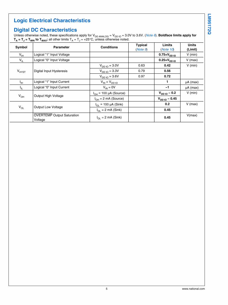
Logic Electrical Characteristics
Digital DC CharacteristicsUnless otherwise noted, these specifications apply for VDD ANALOG = VDD IO = 3.0V to 3.6V. (Note 6). Boldface limits apply forTA = TJ = TMIN to TMAX; all other limits TA = TJ = +25°C, unless otherwise noted.
Symbol Parameter ConditionsTypical
(Note 9)
Limits
(Note 10)
Units
(Limit)
VIH Logical "1" Input Voltage 0.75×VDD IO V (min)
VIL Logical "0" Input Voltage 0.25×VDD IO V (max)
VHYST Digital Input Hysteresis
VDD IO = 3.0V 0.63 0.42 V (min)
VDD IO = 3.3V 0.79 0.56
VDD IO = 3.6V 0.97 0.72
IIH Logical “1” Input Current VIN = VDD IO 1 μA (max)
IIL Logical “0” Input Current VIN = 0V −1 μA (max)
VOH Output High VoltageIOH = 100 μA (Source) VDD IO − 0.2 V (min)
IOH = 2 mA (Source) VDD IO − 0.45
VOL Output Low VoltageIOL = 100 μA (Sink) 0.2 V (max)
IOL = 2 mA (Sink) 0.45
OVERTEMP Output Saturation
VoltageIOL = 2 mA (Sink)
0.45
V(max)
5 www.national.com
LM
95172Q
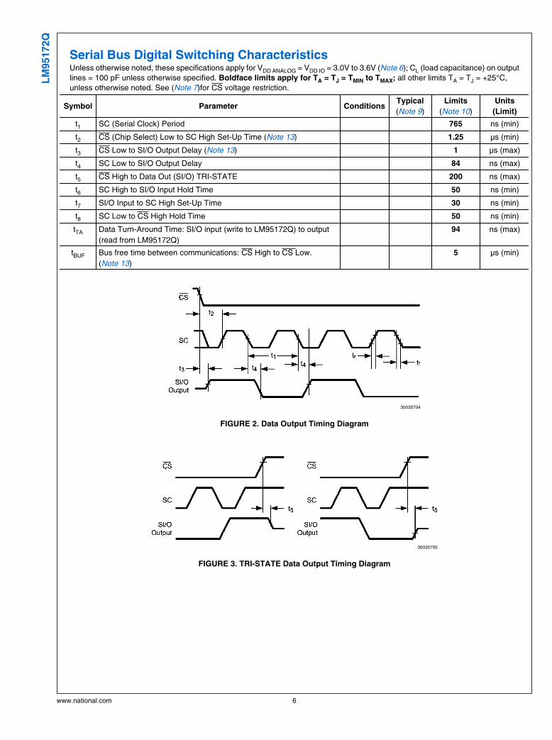
Serial Bus Digital Switching CharacteristicsUnless otherwise noted, these specifications apply for VDD ANALOG = VDD IO = 3.0V to 3.6V (Note 6); CL (load capacitance) on outputlines = 100 pF unless otherwise specified. Boldface limits apply for TA = TJ = TMIN to TMAX; all other limits TA = TJ = +25°C,unless otherwise noted. See (Note 7)for CS voltage restriction.
Symbol Parameter ConditionsTypical
(Note 9)
Limits
(Note 10)
Units
(Limit)
t1 SC (Serial Clock) Period 765 ns (min)
t2 CS (Chip Select) Low to SC High Set-Up Time (Note 13) 1.25 µs (min)
t3 CS Low to SI/O Output Delay (Note 13) 1 µs (max)
t4 SC Low to SI/O Output Delay 84 ns (max)
t5 CS High to Data Out (SI/O) TRI-STATE 200 ns (max)
t6 SC High to SI/O Input Hold Time 50 ns (min)
t7 SI/O Input to SC High Set-Up Time 30 ns (min)
t8 SC Low to CS High Hold Time 50 ns (min)
tTA Data Turn-Around Time: SI/O input (write to LM95172Q) to output
(read from LM95172Q)
94 ns (max)
tBUF Bus free time between communications: CS High to CS Low.
(Note 13)
5 µs (min)
30035704
FIGURE 2. Data Output Timing Diagram
30035705
FIGURE 3. TRI-STATE Data Output Timing Diagram
www.national.com 6
LM
95172Q
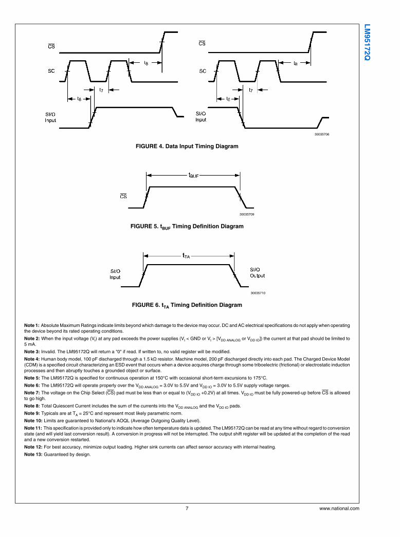
30035706
FIGURE 4. Data Input Timing Diagram
30035709
FIGURE 5. tBUF Timing Definition Diagram
30035710
FIGURE 6. tTA Timing Definition Diagram
Note 1: Absolute Maximum Ratings indicate limits beyond which damage to the device may occur. DC and AC electrical specifications do not apply when operatingthe device beyond its rated operating conditions.
Note 2: When the input voltage (VI) at any pad exceeds the power supplies (VI < GND or VI > [VDD ANALOG or VDD IO]) the current at that pad should be limited to5 mA.
Note 3: Invalid. The LM95172Q will return a "0" if read. If written to, no valid register will be modified.
Note 4: Human body model, 100 pF discharged through a 1.5 kΩ resistor. Machine model, 200 pF discharged directly into each pad. The Charged Device Model(CDM) is a specified circuit characterizing an ESD event that occurs when a device acquires charge through some triboelectric (frictional) or electrostatic inductionprocesses and then abruptly touches a grounded object or surface.
Note 5: The LM95172Q is specified for continuous operation at 150°C with occasional short-term excursions to 175°C.
Note 6: The LM95172Q will operate properly over the VDD ANALOG = 3.0V to 5.5V and VDD IO = 3.0V to 5.5V supply voltage ranges.
Note 7: The voltage on the Chip Select (CS) pad must be less than or equal to (VDD IO +0.2V) at all times. VDD IO must be fully powered-up before CS is allowedto go high.
Note 8: Total Quiescent Current includes the sum of the currents into the VDD ANALOG and the VDD IO pads.
Note 9: Typicals are at TA = 25°C and represent most likely parametric norm.
Note 10: Limits are guaranteed to National's AOQL (Average Outgoing Quality Level).
Note 11: This specification is provided only to indicate how often temperature data is updated. The LM95172Q can be read at any time without regard to conversionstate (and will yield last conversion result). A conversion in progress will not be interrupted. The output shift register will be updated at the completion of the readand a new conversion restarted.
Note 12: For best accuracy, minimize output loading. Higher sink currents can affect sensor accuracy with internal heating.
Note 13: Guaranteed by design.
7 www.national.com
LM
95172Q
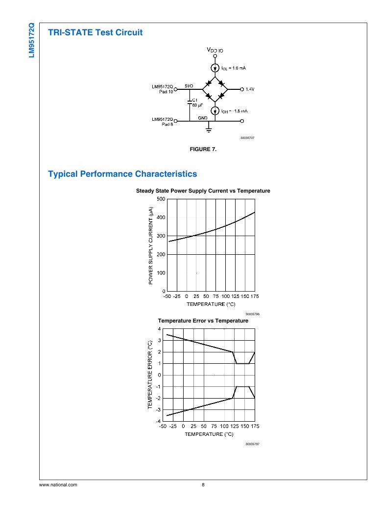
TRI-STATE Test Circuit
30035707
FIGURE 7.
Typical Performance Characteristics
Steady State Power Supply Current vs Temperature
30035796
Temperature Error vs Temperature
30035797
www.national.com 8
LM
95172Q
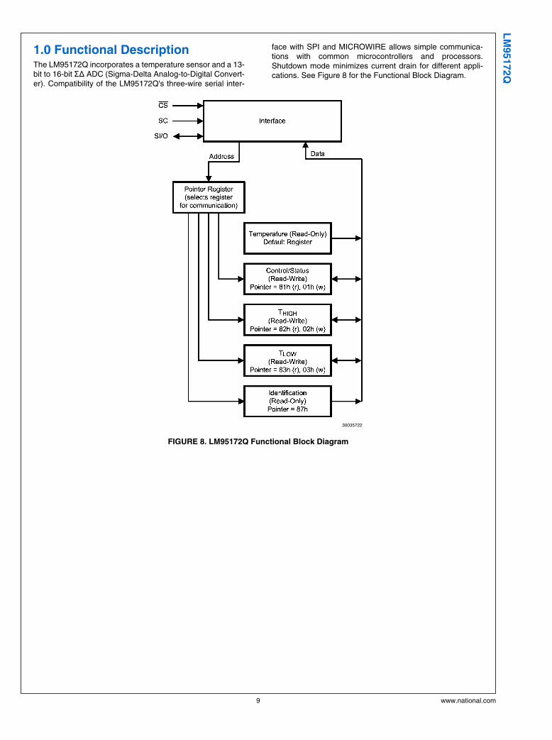
1.0 Functional DescriptionThe LM95172Q incorporates a temperature sensor and a 13-bit to 16-bit ΣΔ ADC (Sigma-Delta Analog-to-Digital Convert-er). Compatibility of the LM95172Q's three-wire serial inter-
face with SPI and MICROWIRE allows simple communica-tions with common microcontrollers and processors.Shutdown mode minimizes current drain for different appli-cations. See Figure 8 for the Functional Block Diagram.
30035722
FIGURE 8. LM95172Q Functional Block Diagram
9 www.national.com
LM
95172Q
1.1 INITIAL SOFTWARE RESET AND POWER-UPSEQUENCES AND POWER ON RESET (POR)
1.1.1 Software Reset Sequence
A software reset sequence must be followed, after the initialVDD ANALOG and VDD IO supply voltages reach their specifiedminimum operating voltages, in order to ensure proper oper-ation of the LM95172Q.
The software reset sequence is as follows:
1. Allow VDD ANALOG and VDD IO to reach their specified mini-mum operating voltages, as specified in the Operating Rat-ings section, and in a manner as specified in section 1.1.2below.
2. Write a “1” to the Shutdown bit, Bit 15 of the Control/StatusRegister, and hold it high for at least the specified maximumconversion time for the initial default of 13-bits resolution, inorder to ensure that a complete reset operation has occurred.(See the Temperature Conversion Time specifications withinthe Temperature-to-Digital Characteristics section.)
3. Write a “0” to the Shutdown bit to restore the LM95172Q tonormal mode.
4. Wait for at least the specified maximum conversion time forthe initial default of 13-bits resolution in order to ensure thataccurate data appears in the Temperature Register.
1.1.2 Power-Up Sequence
A. Linear Power-up
In the case where the VDD ANALOG and VDD IO voltage-vs.-timefunction is linear, the specified minimum operating voltagemust be reached in 5 ms or less.
B. Resistor-Capacitor (R-C) Charging Exponential Power-up
In the case where the VDD ANALOG and VDD IO voltage-vs.-timefunction is as a typical R-C Charging exponential function thetime constant must be less than or equal to 1.25 ms.
C. Other Power-up Functions
In the case where the VDD ANALOG and VDD IO voltage-vs.-timecharacteristic follows another function the following require-ments must be met:
(1) The specified minimum operating voltage values for VDD
ANALOG and VDD IO must be reached in 5 ms or less.
(2) The slope of the VDD ANALOG and VDD IO power-up curvesmust be greater than or equal to 0.7 V/ms at any time beforethe specified minimum operating voltage is reached.
(3) The slope of the VDD ANALOG and VDD IO power-up curvesmust not allow ringing such that the voltage is allowed to dropbelow the specified minimum operating voltage at any timeafter the specified minimum operating voltage is reached.
1.1.3 Power On Reset (POR)
After the requirements of section 1.1.1 and 1.1.2 above aremet each register will then contain its defined POR defaultvalue. Any of the following actions may cause register valuesto change from their POR value:
1. The master writes different data to any Read/Write (R/W)bits, or
2. The LM95172Q is powered down.
The specific POR Value of each register is listed in Section1.7 under Internal Register Structure.
www.national.com 10
LM
95172Q
1.2 ONE SHOT CONVERSION
The LM95172Q features a one-shot conversion bit, which isused to initiate a singe conversion and comparison cyclewhen the LM95172Q is in shutdown mode. While theLM95172Q is in shutdown mode, writing a "1" to the One-Shotbit in the Control/Status Register will cause the LM95172Q toperform a single temperature conversion and update theTemperature Register and the affected status bits. Operatingthe LM95172Q in this one-shot mode allows for extremely lowaverage-power comsumption, making it ideal for low-powerapplications.
When the One-shot bit is set, the LM95172Q initiates a tem-perature conversion. After this initiation, but before the com-pletion of the conversion, and resultant register updates, theLM95172Q is in a "one-shot" state. During this state, the DataAvailable (DAV) flag in the Control/Status Register is "0" andthe Temperature Register contains the value 8000h (-256°C).
All other registers contain the data that was present beforeinitiating the one-shot conversion. After the temperature mea-surement is complete, the DAV flag will be set to "1" and thetemperature register will contain the resultant measured tem-perature.
1.3 OVERTEMP OUTPUT
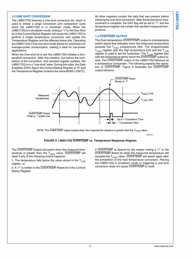
The Over-temperature (OVERTEMP) output is a temperatureswitch signal that indicates when the measured temperatureexceeds the THIGH programmed limit. The programmableTHIGH register sets the high temperature limit and the TLOWregister is used to set the hysteresis. The TLOW register alsosets the temperature below which the OVERTEMP output re-sets. The OVERTEMP output of the LM95172Q behaves asa temperature comparator. The following explains the opera-tion of OVERTEMP. Figure 9 illustrates the OVERTEMPoutput behavior.
30035721
FIGURE 9. LM95172Q OVERTEMP vs. Temperature Response Diagram
The OVERTEMP Output will assert when the measured tem-perature is greater than the THIGH value. OVERTEMP willreset if any of the following events happens:
1. The temperature falls below the value stored in the TLOWregister, or
2. A "1" is written to the OVERTEMP Reset bit in the Control/Status Register.
If OVERTEMP is cleared by the master writing a "1" to theOVERTEMP Reset bit while the measured temperature stillexceeds the THIGH value, OVERTEMP will assert again afterthe completion of the next temperature conversion. Placingthe LM95172Q in shutdown mode or triggering a one-shotconversion does not cause OVERTEMP to reset.
11 www.national.com
LM
95172Q
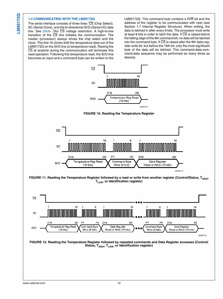
1.4 COMMUNICATING WITH THE LM95172Q
The serial interface consists of three lines: CS (Chip Select),SC (Serial Clock), and the bi-directional SI/O (Serial I/O) dataline. See (Note 7)for CS voltage restriction. A high-to-lowtransition of the CS line initiates the communication. Themaster (processor) always drives the chip select and theclock. The first 16 clocks shift the temperature data out of theLM95172Q on the SI/O line (a temperature read). Raising theCS at anytime during the communication will terminate thisread operation. Following this temperature read, the SI/O linebecomes an input and a command byte can be written to the
LM95172Q. This command byte contains a R/W bit and theaddress of the register to be communicated with next (seeSection 1.7 Internal Register Structure). When writing, thedata is latched in after every 8 bits. The processor must writeat least 8 bits in order to latch the data. If CS is raised beforethe falling edge of the 8th command bit, no data will be latchedinto the command byte. If CS is raised after the 8th data-reg-ister write bit, but before the 16th bit, only the most significantbyte of the data will be latched. This command-data-com-mand-data sequence may be performed as many times asdesired.
30035714
FIGURE 10. Reading the Temperature Register
30035716
FIGURE 11. Reading the Temperature Register followed by a read or write from another register (Control/Status, THIGH,TLOW, or Identification register)
30035715
FIGURE 12. Reading the Temperature Register followed by repeated commands and Data Register accesses (Control/Status, THIGH, TLOW, or Identification register)
www.national.com 12
LM
95172Q
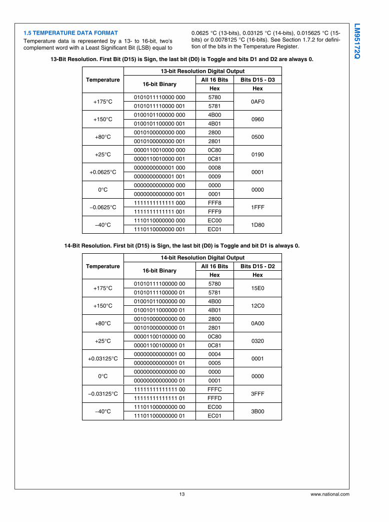
1.5 TEMPERATURE DATA FORMAT
Temperature data is represented by a 13- to 16-bit, two'scomplement word with a Least Significant Bit (LSB) equal to
0.0625 °C (13-bits), 0.03125 °C (14-bits), 0.015625 °C (15-bits) or 0.0078125 °C (16-bits). See Section 1.7.2 for defini-tion of the bits in the Temperature Register.
13-Bit Resolution. First Bit (D15) is Sign, the last bit (D0) is Toggle and bits D1 and D2 are always 0.
Temperature
13-bit Resolution Digital Output
16-bit BinaryAll 16 Bits Bits D15 - D3
Hex Hex
+175°C0101011110000 000 5780
0AF00101011110000 001 5781
+150°C0100101100000 000 4B00
09600100101100000 001 4B01
+80°C0010100000000 000 2800
05000010100000000 001 2801
+25°C0000110010000 000 0C80
01900000110010000 001 0C81
+0.0625°C0000000000001 000 0008
00010000000000001 001 0009
0°C0000000000000 000 0000
00000000000000000 001 0001
−0.0625°C1111111111111 000 FFF8
1FFF1111111111111 001 FFF9
−40°C1110110000000 000 EC00
1D801110110000000 001 EC01
14-Bit Resolution. First bit (D15) is Sign, the last bit (D0) is Toggle and bit D1 is always 0.
Temperature
14-bit Resolution Digital Output
16-bit BinaryAll 16 Bits Bits D15 - D2
Hex Hex
+175°C01010111100000 00 5780
15E001010111100000 01 5781
+150°C01001011000000 00 4B00
12C001001011000000 01 4B01
+80°C00101000000000 00 2800
0A0000101000000000 01 2801
+25°C00001100100000 00 0C80
032000001100100000 01 0C81
+0.03125°C00000000000001 00 0004
000100000000000001 01 0005
0°C00000000000000 00 0000
000000000000000000 01 0001
−0.03125°C11111111111111 00 FFFC
3FFF11111111111111 01 FFFD
−40°C11101100000000 00 EC00
3B0011101100000000 01 EC01
13 www.national.com
LM
95172Q
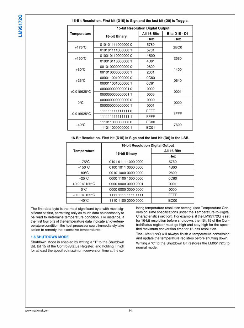
15-Bit Resolution. First bit (D15) is Sign and the last bit (D0) is Toggle.
Temperature
15-bit Resolution Digital Output
16-bit BinaryAll 16 Bits Bits D15 - D1
Hex Hex
+175°C010101111000000 0 5780
2BC0010101111000000 1 5781
+150°C010010110000000 0 4B00
2580010010110000000 1 4B01
+80°C001010000000000 0 2800
1400001010000000000 1 2801
+25°C000011001000000 0 0C80
0640000011001000000 1 0C81
+0.015625°C000000000000001 0 0002
0001000000000000001 1 0003
0°C000000000000000 0 0000
0000000000000000000 1 0001
−0.015625°C111111111111111 0 FFFE
7FFF111111111111111 1 FFFF
−40°C111011000000000 0 EC00
7600111011000000000 1 EC01
16-Bit Resolution. First bit (D15) is Sign and the last bit (D0) is the LSB.
Temperature
16-bit Resolution Digital Output
16-bit BinaryAll 16 Bits
Hex
+175°C 0101 0111 1000 0000 5780
+150°C 0100 1011 0000 0000 4B00
+80°C 0010 1000 0000 0000 2800
+25°C 0000 1100 1000 0000 0C80
+0.0078125°C 0000 0000 0000 0001 0001
0°C 0000 0000 0000 0000 0000
−0.0078125°C 1111 1111 1111 1111 FFFF
−40°C 1110 1100 0000 0000 EC00
The first data byte is the most significant byte with most sig-nificant bit first, permitting only as much data as necessary tobe read to determine temperature condition. For instance, ifthe first four bits of the temperature data indicate an overtem-perature condition, the host processor could immediately takeaction to remedy the excessive temperatures.
1.6 SHUTDOWN MODE
Shutdown Mode is enabled by writing a “1” to the ShutdownBit, Bit 15 of the Control/Status Register, and holding it highfor at least the specified maximum conversion time at the ex-
isting temperature resolution setting. (see Temperature Con-version Time specifications under the Temperature-to-DigitalCharacteristics section). For example, if the LM95172Q is setfor 16-bit resolution before shutdown, then Bit 15 of the Con-trol/Status register must go high and stay high for the speci-fied maximum conversion time for 16-bits resolution.
The LM95172Q will always finish a temperature conversionand update the temperature registers before shutting down.
Writing a “0” to the Shutdown Bit restores the LM95172Q tonormal mode.
www.national.com 14
LM
95172Q
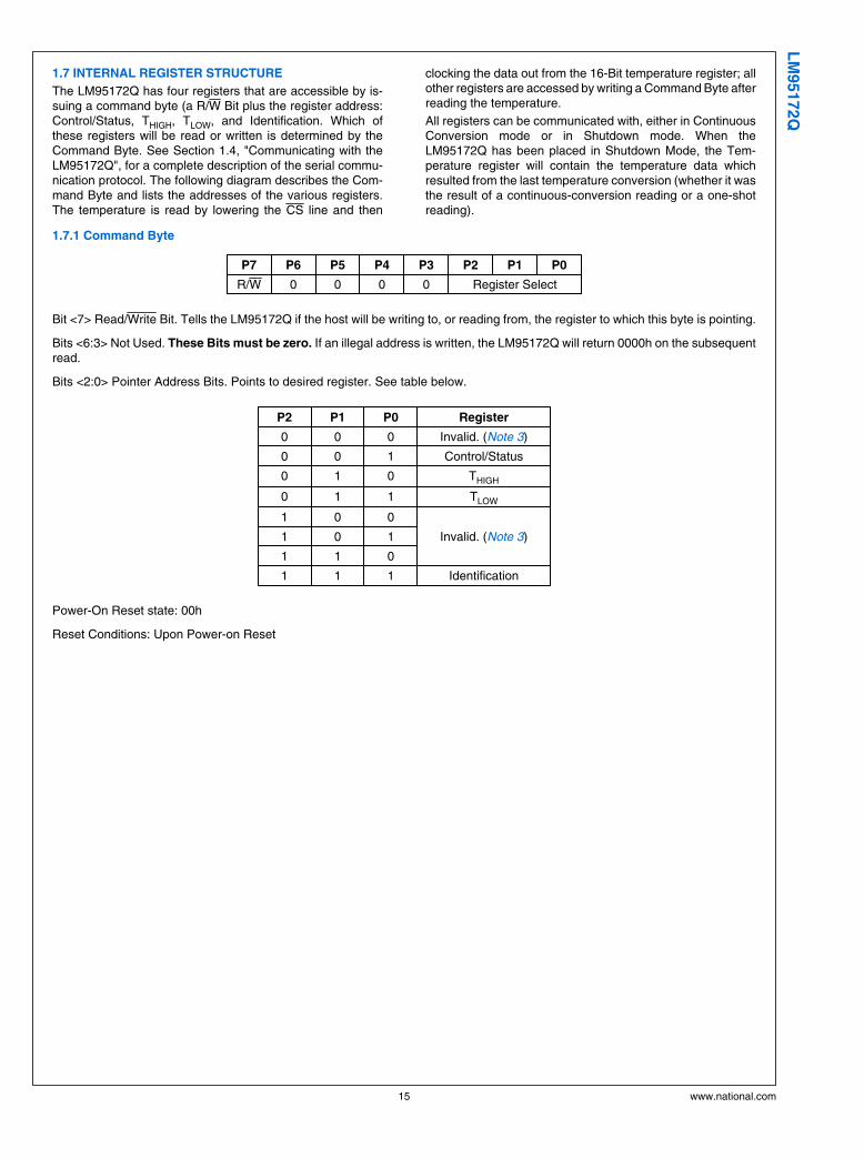
1.7 INTERNAL REGISTER STRUCTURE
The LM95172Q has four registers that are accessible by is-suing a command byte (a R/W Bit plus the register address:Control/Status, THIGH, TLOW, and Identification. Which ofthese registers will be read or written is determined by theCommand Byte. See Section 1.4, "Communicating with theLM95172Q", for a complete description of the serial commu-nication protocol. The following diagram describes the Com-mand Byte and lists the addresses of the various registers.The temperature is read by lowering the CS line and then
clocking the data out from the 16-Bit temperature register; allother registers are accessed by writing a Command Byte afterreading the temperature.
All registers can be communicated with, either in ContinuousConversion mode or in Shutdown mode. When theLM95172Q has been placed in Shutdown Mode, the Tem-perature register will contain the temperature data whichresulted from the last temperature conversion (whether it wasthe result of a continuous-conversion reading or a one-shotreading).
1.7.1 Command Byte
P7 P6 P5 P4 P3 P2 P1 P0
R/W 0 0 0 0 Register Select
Bit <7> Read/Write Bit. Tells the LM95172Q if the host will be writing to, or reading from, the register to which this byte is pointing.
Bits <6:3> Not Used. These Bits must be zero. If an illegal address is written, the LM95172Q will return 0000h on the subsequentread.
Bits <2:0> Pointer Address Bits. Points to desired register. See table below.
P2 P1 P0 Register
0 0 0 Invalid. (Note 3)
0 0 1 Control/Status
0 1 0 THIGH
0 1 1 TLOW
1 0 0
Invalid. (Note 3)1 0 1
1 1 0
1 1 1 Identification
Power-On Reset state: 00h
Reset Conditions: Upon Power-on Reset
15 www.national.com
LM
95172Q
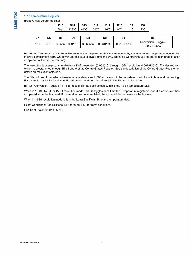
1.7.2 Temperature Register
(Read Only): Default Register
D15 D14 D13 D12 D11 D10 D9 D8
Sign 128°C 64°C 32°C 16°C 8°C 4°C 2°C
D7 D6 D5 D4 D3 D2 D1 D0
1°C 0.5°C 0.25°C 0.125°C 0.0625°C 0.03125°C 0.015625°CConversion - Toggle/
0.0078125°C
Bit <15:1>: Temperature Data Byte. Represents the temperature that was measured by the most recent temperature conversionin two's complement form. On power-up, this data is invalid until the DAV Bit in the Control/Status Register is high (that is, aftercompletion of the first conversion).
The resolution is user-programmable from 13-Bit resolution (0.0625°C) through 16-Bit resolution (0.0078125°C). The desired res-olution is programmed through Bits 4 and 5 of the Control/Status Register. See the description of the Control/Status Register fordetails on resolution selection.
The Bits not used for a selected resolution are always set to "0" and are not to be considered part of a valid temperature reading.For example, for 14-Bit resolution, Bit <1> is not used and, therefore, it is invalid and is always zero.
Bit <0>: Conversion Toggle or, if 16-Bit resolution has been selected, this is the 16-Bit temperature LSB.
When in 13-Bit, 14-Bit, or 15-Bit resolution mode, this Bit toggles each time the Temperature register is read if a conversion hascompleted since the last read. If conversion has not completed, the value will be the same as the last read.
When in 16-Bit resolution mode, this is the Least Significant Bit of the temperature data.
Reset Conditions: See Sections 1.1.1 through 1.1.3 for reset conditions.
One-Shot State: 8000h (-256°C)
www.national.com 16
LM
95172Q
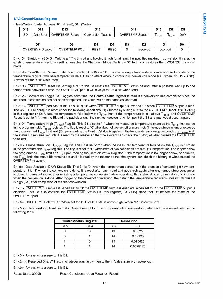
1.7.3 Control/Status Register
(Read/Write) Pointer Address: 81h (Read); 01h (Write)
D15 D14 D13 D12 D11 D10 D9 D8
SD One-Shot OVERTEMP Reset Conversion Toggle OVERTEMP Status THIGH TLOW DAV
D7 D6 D5 D4 D3 D2 D1 D0
OVERTEMP Disable OVERTEMP POL RES1 RES0 0 reserved reserved 0
Bit <15>: Shutdown (SD) Bit. Writing a “1” to this bit and holding it high for at least the specified maximum conversion time, at theexisting temperature resolution setting, enables the Shutdown Mode. Writing a “0” to this bit restores the LM95172Q to normalmode.
Bit <14>: One-Shot Bit. When in shutdown mode (Bit <15> is "1"), initates a single temperature conversion and update of thetemperature register with new temperature data. Has no effect when in continuous conversion mode (i.e., when Bit <15> is "0").Always returns a "0" when read.
Bit <13>: OVERTEMP Reset Bit. Writing a "1" to this Bit resets the OVERTEMP Status bit and, after a possible wait up to onetemperature conversion time, the OVERTEMP pad. It will always return a "0" when read.
Bit <12>: Conversion Toggle Bit. Toggles each time the Control/Status register is read if a conversion has completed since thelast read. If conversion has not been completed, the value will be the same as last read.
Bit <11>: OVERTEMP pad Status Bit. This Bit is "0" when OVERTEMP output is low and "1" when OVERTEMP output is high.The OVERTEMP output is reset under the following conditions: (1) Cleared by writing a "1" to the OVERTEMP Reset Bit (Bit <13>)in this register or (2) Measured temperature falls below the TLOW limit. If the temperature is still above THIGH, and OVERTEMPReset is set to "1", then the Bit and the pad clear until the next conversion, at which point the Bit and pad would assert again.
Bit <10>: Temperature High (THIGH) Flag Bit. This Bit is set to "1" when the measured temperature exceeds the THIGH limit storedin the programmable THIGH register. The flag is reset to "0" when both of two conditions are met: (1) temperature no longer exceedsthe programmed THIGH limit and (2) upon reading the Control/Status Register. If the temperature no longer exceeds the THIGH limit,the status Bit remains set until it is read by the master so that the system can check the history of what caused the OVERTEMPto assert.
Bit <9>: Temperature Low (TLOW) Flag Bit. This Bit is set to "1" when the measured temperature falls below the TLOW limit storedin the programmable TLOW register. The flag is reset to "0" when both of two conditions are met: (1) temperature is no longer belowthe programmed TLOW limit and (2) upon reading the Control/Status Register. If the temperature is no longer below, or equal to,the TLOW limit, the status Bit remains set until it is read by the master so that the system can check the history of what caused theOVERTEMP to assert.
Bit <8>: Data Available (DAV) Status Bit. This Bit is "0" when the temperature sensor is in the process of converting a new tem-perature. It is "1" when the conversion is done. It is reset after each read and goes high again after one temperature conversionis done. In one-shot mode: after initiating a temperature conversion while operating, this status Bit can be monitored to indicatewhen the conversion is done. After triggering the one-shot conversion, the data in the temperature register is invalid until this Bitis high (i.e., after completion of the first conversion).
Bit <7>: OVERTEMP Disable Bit. When set to "0" the OVERTEMP output is enabled. When set to "1" the OVERTEMP output isdisabled. This Bit also controls the OVERTEMP Status Bit (this register, Bit <11>) since that Bit reflects the state of theOVERTEMP pad.
Bit <6>: OVERTEMP Polarity Bit. When set to "1", OVERTEMP is active-high. When "0" it is active-low.
Bit <5:4>: Temperature Resolution Bits. Selects one of four user-programmable temperature data resolutions as indicated in thefollowing table.
Control/Status Register Resolution
Bit 5 Bit 4 Bits °C
0 0 13 0.0625
0 1 14 0.03125
1 0 15 0.015625
1 1 16 0.0078125
Bit <3>: Always write a zero to this Bit.
Bit <2:1>: Reserved Bits. Will return whatever was last written to them. Value is zero on power-up.
Bit <0>: Always write a zero to this Bit.
Reset State: 0000h Reset Conditions: Upon Power-on Reset.
17 www.national.com
LM
95172Q
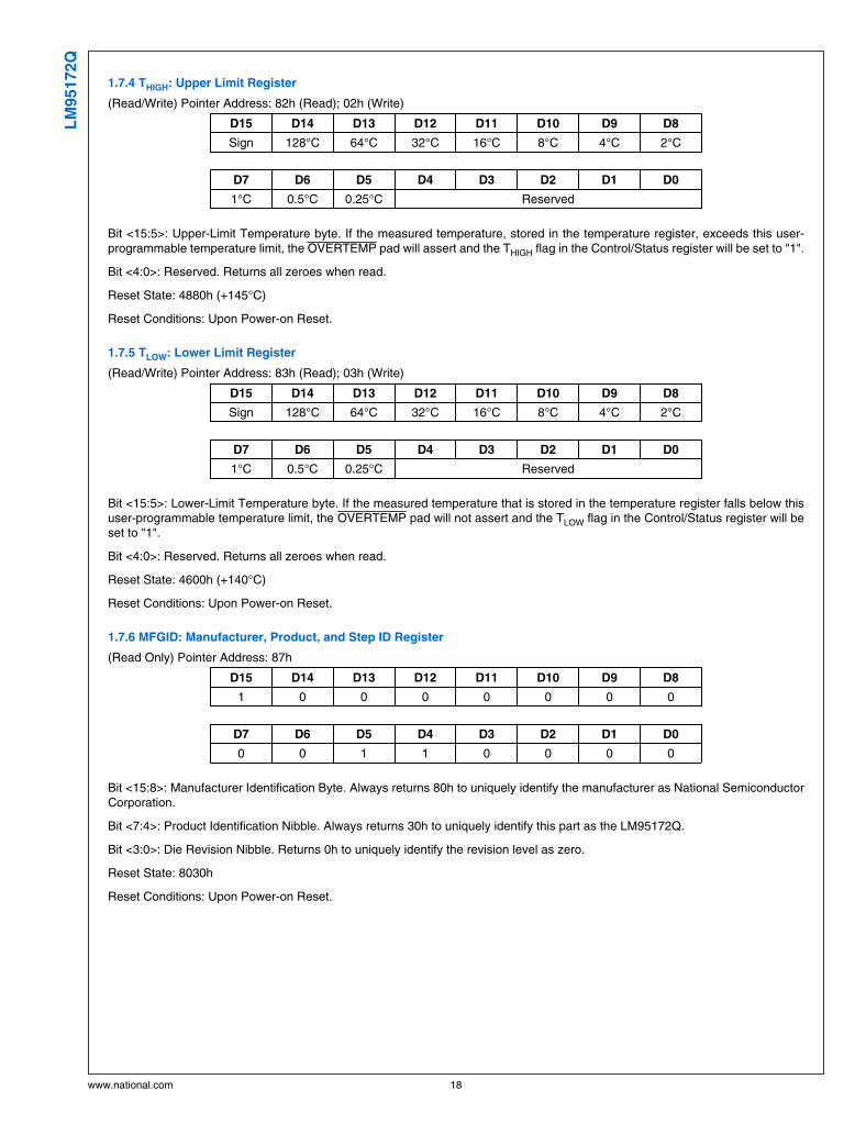
1.7.4 THIGH: Upper Limit Register
(Read/Write) Pointer Address: 82h (Read); 02h (Write)
D15 D14 D13 D12 D11 D10 D9 D8
Sign 128°C 64°C 32°C 16°C 8°C 4°C 2°C
D7 D6 D5 D4 D3 D2 D1 D0
1°C 0.5°C 0.25°C Reserved
Bit <15:5>: Upper-Limit Temperature byte. If the measured temperature, stored in the temperature register, exceeds this user-programmable temperature limit, the OVERTEMP pad will assert and the THIGH flag in the Control/Status register will be set to "1".
Bit <4:0>: Reserved. Returns all zeroes when read.
Reset State: 4880h (+145°C)
Reset Conditions: Upon Power-on Reset.
1.7.5 TLOW: Lower Limit Register
(Read/Write) Pointer Address: 83h (Read); 03h (Write)
D15 D14 D13 D12 D11 D10 D9 D8
Sign 128°C 64°C 32°C 16°C 8°C 4°C 2°C
D7 D6 D5 D4 D3 D2 D1 D0
1°C 0.5°C 0.25°C Reserved
Bit <15:5>: Lower-Limit Temperature byte. If the measured temperature that is stored in the temperature register falls below thisuser-programmable temperature limit, the OVERTEMP pad will not assert and the TLOW flag in the Control/Status register will beset to "1".
Bit <4:0>: Reserved. Returns all zeroes when read.
Reset State: 4600h (+140°C)
Reset Conditions: Upon Power-on Reset.
1.7.6 MFGID: Manufacturer, Product, and Step ID Register
(Read Only) Pointer Address: 87h
D15 D14 D13 D12 D11 D10 D9 D8
1 0 0 0 0 0 0 0
D7 D6 D5 D4 D3 D2 D1 D0
0 0 1 1 0 0 0 0
Bit <15:8>: Manufacturer Identification Byte. Always returns 80h to uniquely identify the manufacturer as National SemiconductorCorporation.
Bit <7:4>: Product Identification Nibble. Always returns 30h to uniquely identify this part as the LM95172Q.
Bit <3:0>: Die Revision Nibble. Returns 0h to uniquely identify the revision level as zero.
Reset State: 8030h
Reset Conditions: Upon Power-on Reset.
www.national.com 18
LM
95172Q
1.8 NOISE IMMUNITY OF THE SERIAL I/O (SI/O) ANDSERIAL CLOCK (SC) LINES
The LM95172Q's Serial I/O and Serial Clock lines have highnoise immunity making it an excellent choice in challengingelectromagnetic environments.
Some typical bench tests, taken at room temperature, weredone to show the noise immunity in the case of an injectedsinewave signal used to simulate an interfering noise signal.
Figure 13 below shows the Test Setup used for the benchtest. A function generator was used to create the noise signal.I the first test this signal was AC-coupled to the SI/O linethrough a 1 nF capacitor. The amplitude of the signal from thegenerator was adjusted so that the peak-to-peak voltage atthe pad was 400 mVpp, the maximum that is compatible withthe Absolute Maximum requirements.
30035711
FIGURE 13. Test Setup for Noise Immunity Test
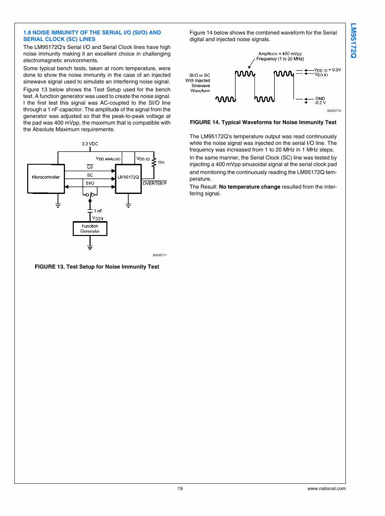
Figure 14 below shows the combined waveform for the Serialdigital and injected noise signals.
30035712
FIGURE 14. Typical Waveforms for Noise Immunity Test
The LM95172Q's temperature output was read continuouslywhile the noise signal was injected on the serial I/O line. Thefrequency was increased from 1 to 20 MHz in 1 MHz steps.
In the same manner, the Serial Clock (SC) line was tested byinjecting a 400 mVpp sinusoidal signal at the serial clock pad
and monitoring the continuously reading the LM95172Q tem-perature.
The Result: No temperature change resulted from the inter-fering signal.
19 www.national.com
LM
95172Q
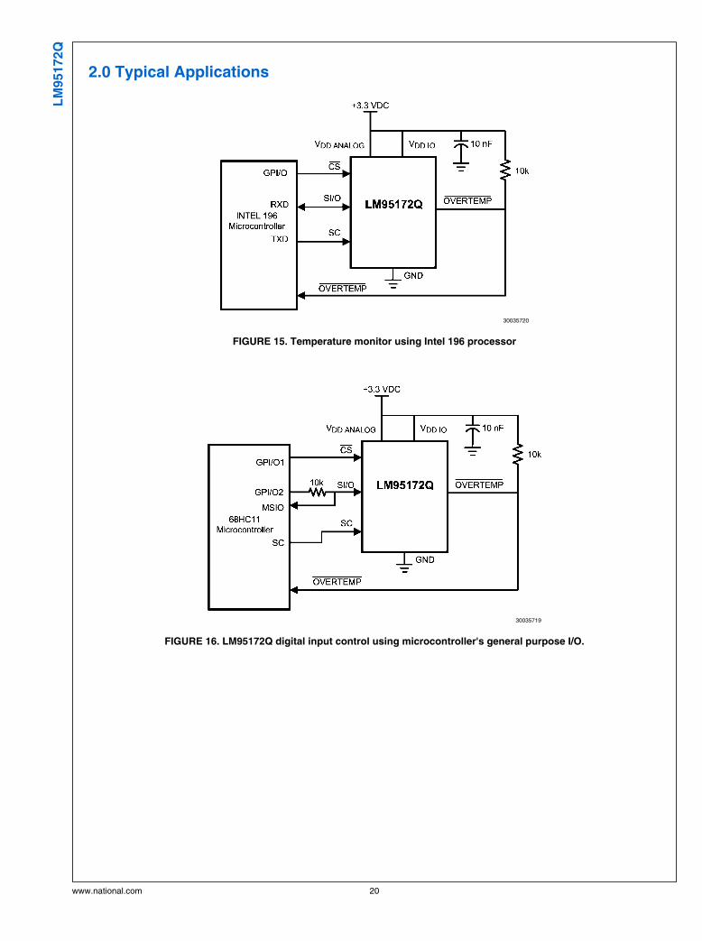
2.0 Typical Applications
30035720
FIGURE 15. Temperature monitor using Intel 196 processor
30035719
FIGURE 16. LM95172Q digital input control using microcontroller's general purpose I/O.
www.national.com 20
LM
95172Q
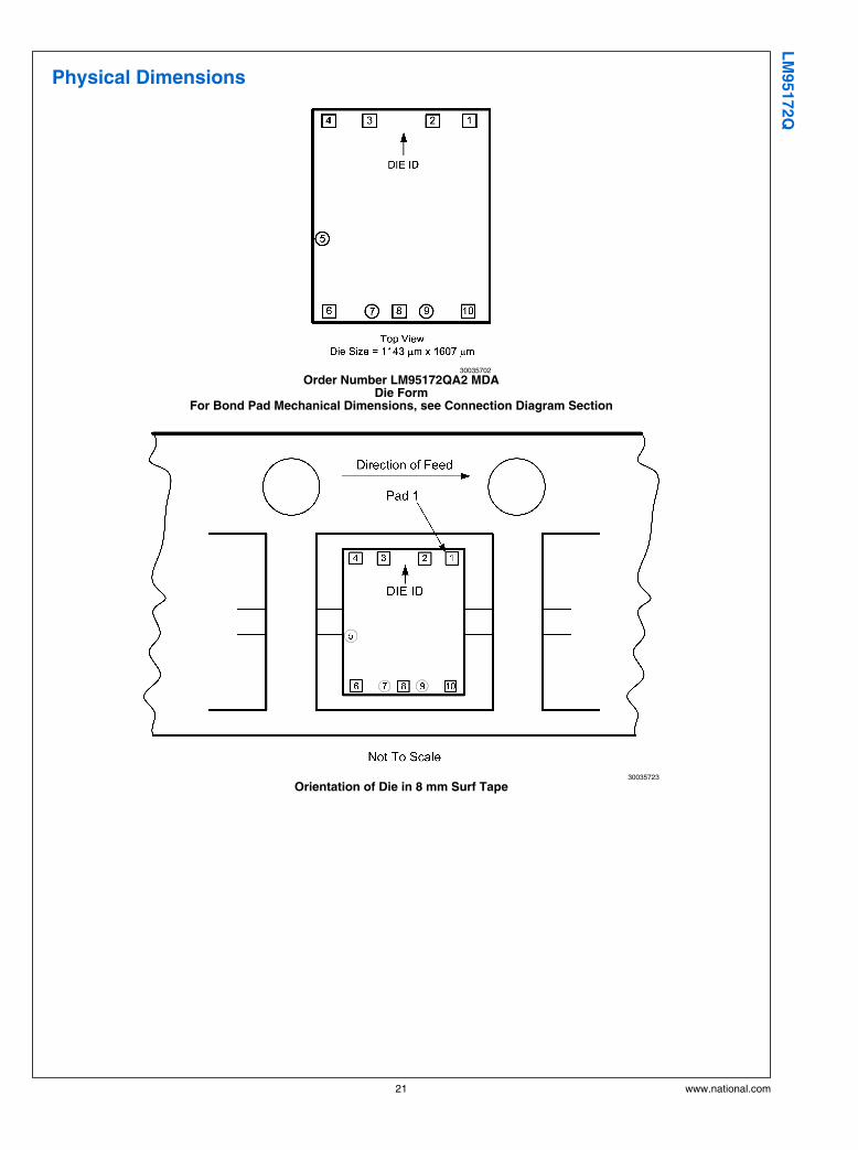
Physical Dimensions
30035702
Order Number LM95172QA2 MDADie Form
For Bond Pad Mechanical Dimensions, see Connection Diagram Section
30035723
Orientation of Die in 8 mm Surf Tape
21 www.national.com
LM
95172Q
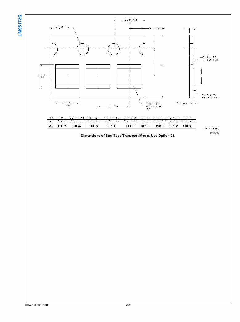
30035799
Dimensions of Surf Tape Transport Media. Use Option 01.
www.national.com 22
LM
95172Q
Notes
23 www.national.com
LM
95172Q
NotesL
M95172Q
Dig
ital T
em
pera
ture
Sen
so
r in
Die
Fo
rm w
ith
± 1
°C A
ccu
racy f
rom
130°C
to
160°C
For more National Semiconductor product information and proven design tools, visit the following Web sites at:
www.national.com
Products Design Support
Amplifiers www.national.com/amplifiers WEBENCH® Tools www.national.com/webench
Audio www.national.com/audio App Notes www.national.com/appnotes
Clock and Timing www.national.com/timing Reference Designs www.national.com/refdesigns
Data Converters www.national.com/adc Samples www.national.com/samples
Interface www.national.com/interface Eval Boards www.national.com/evalboards
LVDS www.national.com/lvds Packaging www.national.com/packaging
Power Management www.national.com/power Green Compliance www.national.com/quality/green
Switching Regulators www.national.com/switchers Distributors www.national.com/contacts
LDOs www.national.com/ldo Quality and Reliability www.national.com/quality
LED Lighting www.national.com/led Feedback/Support www.national.com/feedback
Voltage References www.national.com/vref Design Made Easy www.national.com/easy
PowerWise® Solutions www.national.com/powerwise Applications & Markets www.national.com/solutions
Serial Digital Interface (SDI) www.national.com/sdi Mil/Aero www.national.com/milaero
Temperature Sensors www.national.com/tempsensors SolarMagic™ www.national.com/solarmagic
PLL/VCO www.national.com/wireless PowerWise® DesignUniversity
www.national.com/training
THE CONTENTS OF THIS DOCUMENT ARE PROVIDED IN CONNECTION WITH NATIONAL SEMICONDUCTOR CORPORATION(“NATIONAL”) PRODUCTS. NATIONAL MAKES NO REPRESENTATIONS OR WARRANTIES WITH RESPECT TO THE ACCURACYOR COMPLETENESS OF THE CONTENTS OF THIS PUBLICATION AND RESERVES THE RIGHT TO MAKE CHANGES TOSPECIFICATIONS AND PRODUCT DESCRIPTIONS AT ANY TIME WITHOUT NOTICE. NO LICENSE, WHETHER EXPRESS,IMPLIED, ARISING BY ESTOPPEL OR OTHERWISE, TO ANY INTELLECTUAL PROPERTY RIGHTS IS GRANTED BY THISDOCUMENT.
TESTING AND OTHER QUALITY CONTROLS ARE USED TO THE EXTENT NATIONAL DEEMS NECESSARY TO SUPPORTNATIONAL’S PRODUCT WARRANTY. EXCEPT WHERE MANDATED BY GOVERNMENT REQUIREMENTS, TESTING OF ALLPARAMETERS OF EACH PRODUCT IS NOT NECESSARILY PERFORMED. NATIONAL ASSUMES NO LIABILITY FORAPPLICATIONS ASSISTANCE OR BUYER PRODUCT DESIGN. BUYERS ARE RESPONSIBLE FOR THEIR PRODUCTS ANDAPPLICATIONS USING NATIONAL COMPONENTS. PRIOR TO USING OR DISTRIBUTING ANY PRODUCTS THAT INCLUDENATIONAL COMPONENTS, BUYERS SHOULD PROVIDE ADEQUATE DESIGN, TESTING AND OPERATING SAFEGUARDS.
EXCEPT AS PROVIDED IN NATIONAL’S TERMS AND CONDITIONS OF SALE FOR SUCH PRODUCTS, NATIONAL ASSUMES NOLIABILITY WHATSOEVER, AND NATIONAL DISCLAIMS ANY EXPRESS OR IMPLIED WARRANTY RELATING TO THE SALEAND/OR USE OF NATIONAL PRODUCTS INCLUDING LIABILITY OR WARRANTIES RELATING TO FITNESS FOR A PARTICULARPURPOSE, MERCHANTABILITY, OR INFRINGEMENT OF ANY PATENT, COPYRIGHT OR OTHER INTELLECTUAL PROPERTYRIGHT.
LIFE SUPPORT POLICY
NATIONAL’S PRODUCTS ARE NOT AUTHORIZED FOR USE AS CRITICAL COMPONENTS IN LIFE SUPPORT DEVICES ORSYSTEMS WITHOUT THE EXPRESS PRIOR WRITTEN APPROVAL OF THE CHIEF EXECUTIVE OFFICER AND GENERALCOUNSEL OF NATIONAL SEMICONDUCTOR CORPORATION. As used herein:
Life support devices or systems are devices which (a) are intended for surgical implant into the body, or (b) support or sustain life andwhose failure to perform when properly used in accordance with instructions for use provided in the labeling can be reasonably expectedto result in a significant injury to the user. A critical component is any component in a life support device or system whose failure to performcan be reasonably expected to cause the failure of the life support device or system or to affect its safety or effectiveness.
National Semiconductor and the National Semiconductor logo are registered trademarks of National Semiconductor Corporation. All otherbrand or product names may be trademarks or registered trademarks of their respective holders.
Copyright© 2010 National Semiconductor Corporation
For the most current product information visit us at www.national.com
National SemiconductorAmericas TechnicalSupport CenterEmail: [email protected]: 1-800-272-9959
National Semiconductor EuropeTechnical Support CenterEmail: [email protected]
National Semiconductor AsiaPacific Technical Support CenterEmail: [email protected]
National Semiconductor JapanTechnical Support CenterEmail: [email protected]
www.national.com
IMPORTANT NOTICE
Texas Instruments Incorporated and its subsidiaries (TI) reserve the right to make corrections, enhancements, improvements and otherchanges to its semiconductor products and services per JESD46, latest issue, and to discontinue any product or service per JESD48, latestissue. Buyers should obtain the latest relevant information before placing orders and should verify that such information is current andcomplete. All semiconductor products (also referred to herein as “components”) are sold subject to TI’s terms and conditions of salesupplied at the time of order acknowledgment.
TI warrants performance of its components to the specifications applicable at the time of sale, in accordance with the warranty in TI’s termsand conditions of sale of semiconductor products. Testing and other quality control techniques are used to the extent TI deems necessaryto support this warranty. Except where mandated by applicable law, testing of all parameters of each component is not necessarilyperformed.
TI assumes no liability for applications assistance or the design of Buyers’ products. Buyers are responsible for their products andapplications using TI components. To minimize the risks associated with Buyers’ products and applications, Buyers should provideadequate design and operating safeguards.
TI does not warrant or represent that any license, either express or implied, is granted under any patent right, copyright, mask work right, orother intellectual property right relating to any combination, machine, or process in which TI components or services are used. Informationpublished by TI regarding third-party products or services does not constitute a license to use such products or services or a warranty orendorsement thereof. Use of such information may require a license from a third party under the patents or other intellectual property of thethird party, or a license from TI under the patents or other intellectual property of TI.
Reproduction of significant portions of TI information in TI data books or data sheets is permissible only if reproduction is without alterationand is accompanied by all associated warranties, conditions, limitations, and notices. TI is not responsible or liable for such altereddocumentation. Information of third parties may be subject to additional restrictions.
Resale of TI components or services with statements different from or beyond the parameters stated by TI for that component or servicevoids all express and any implied warranties for the associated TI component or service and is an unfair and deceptive business practice.TI is not responsible or liable for any such statements.
Buyer acknowledges and agrees that it is solely responsible for compliance with all legal, regulatory and safety-related requirementsconcerning its products, and any use of TI components in its applications, notwithstanding any applications-related information or supportthat may be provided by TI. Buyer represents and agrees that it has all the necessary expertise to create and implement safeguards whichanticipate dangerous consequences of failures, monitor failures and their consequences, lessen the likelihood of failures that might causeharm and take appropriate remedial actions. Buyer will fully indemnify TI and its representatives against any damages arising out of the useof any TI components in safety-critical applications.
In some cases, TI components may be promoted specifically to facilitate safety-related applications. With such components, TI’s goal is tohelp enable customers to design and create their own end-product solutions that meet applicable functional safety standards andrequirements. Nonetheless, such components are subject to these terms.
No TI components are authorized for use in FDA Class III (or similar life-critical medical equipment) unless authorized officers of the partieshave executed a special agreement specifically governing such use.
Only those TI components which TI has specifically designated as military grade or “enhanced plastic” are designed and intended for use inmilitary/aerospace applications or environments. Buyer acknowledges and agrees that any military or aerospace use of TI componentswhich have not been so designated is solely at the Buyer's risk, and that Buyer is solely responsible for compliance with all legal andregulatory requirements in connection with such use.
TI has specifically designated certain components which meet ISO/TS16949 requirements, mainly for automotive use. Components whichhave not been so designated are neither designed nor intended for automotive use; and TI will not be responsible for any failure of suchcomponents to meet such requirements.
Products Applications
Audio www.ti.com/audio Automotive and Transportation www.ti.com/automotive
Amplifiers amplifier.ti.com Communications and Telecom www.ti.com/communications
Data Converters dataconverter.ti.com Computers and Peripherals www.ti.com/computers
DLP® Products www.dlp.com Consumer Electronics www.ti.com/consumer-apps
DSP dsp.ti.com Energy and Lighting www.ti.com/energy
Clocks and Timers www.ti.com/clocks Industrial www.ti.com/industrial
Interface interface.ti.com Medical www.ti.com/medical
Logic logic.ti.com Security www.ti.com/security
Power Mgmt power.ti.com Space, Avionics and Defense www.ti.com/space-avionics-defense
Microcontrollers microcontroller.ti.com Video and Imaging www.ti.com/video
RFID www.ti-rfid.com
OMAP Applications Processors www.ti.com/omap TI E2E Community e2e.ti.com
Wireless Connectivity www.ti.com/wirelessconnectivity
Mailing Address: Texas Instruments, Post Office Box 655303, Dallas, Texas 75265Copyright © 2012, Texas Instruments Incorporated