Embed Size (px)
Citation preview
Diamond Detector Prototyping
Outline: Recipe “how to make a diamond detector”
1. Buy
2. Clean with various acids/bases
3. Metallize
4. Mount in a nice package and wirebond
5. Tests – checks to see if you did a good job
6. Summary
Anna Micherdzinska
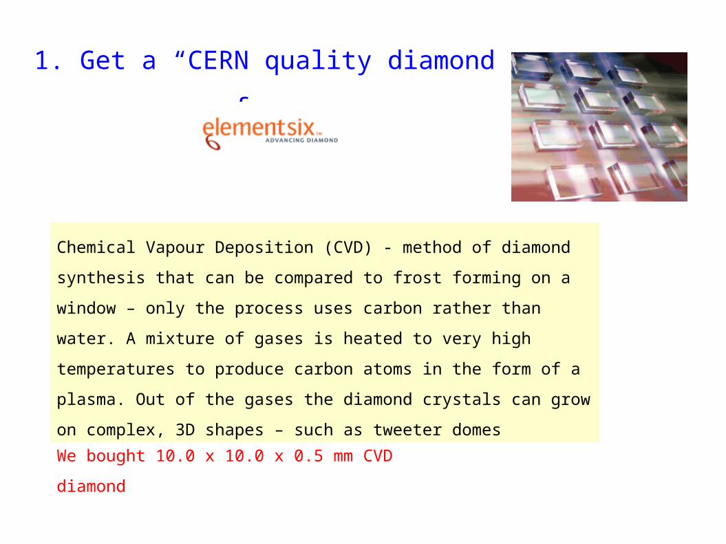
1. Get a “CERN quality diamond from
Chemical Vapour Deposition (CVD) - method of diamond synthesis that
can be compared to frost forming on a window – only the process uses
carbon rather than water. A mixture of gases is heated to very high
temperatures to produce carbon atoms in the form of a plasma. Out of
the gases the diamond crystals can grow on complex, 3D shapes – such
as tweeter domes
We bought 10.0 x 10.0 x 0.5 mm CVD diamond
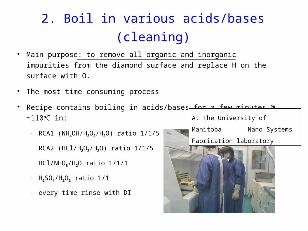
2. Boil in various acids/bases (cleaning)
Main purpose: to remove all organic and inorganic impurities from the
diamond surface and replace H on the surface with O.
The most time consuming process
Recipe contains boiling in acids/bases for a few minutes @ ~110oC in:
RCA1 (NH4OH/H2O2/H2O) ratio 1/1/5
RCA2 (HCl/H2O2/H2O) ratio 1/1/5
HCl/NHO3/H2O ratio 1/1/1
H2SO4/H2O2 ratio 1/1
every time rinse with DI
At The University of Manitoba
Nano-Systems Fabrication laboratory
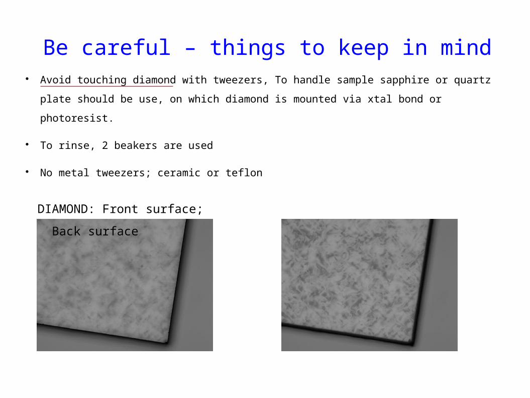
Be careful – things to keep in mind Avoid touching diamond with tweezers, To handle sample sapphire or quartz plate
should be use, on which diamond is mounted via xtal bond or photoresist.
To rinse, 2 beakers are used
No metal tweezers; ceramic or teflon
DIAMOND: Front surface; Back surface
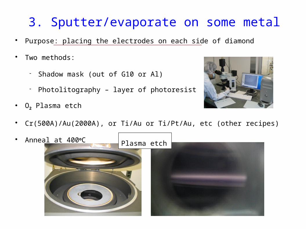
3. Sputter/evaporate on some metal Purpose: placing the electrodes on each side of diamond
Two methods:
Shadow mask (out of G10 or Al)
Photolitography – layer of photoresist
O2 Plasma etch
Cr(500A)/Au(2000A), or Ti/Au or Ti/Pt/Au, etc (other recipes)
Anneal at 400oC Plasma etch
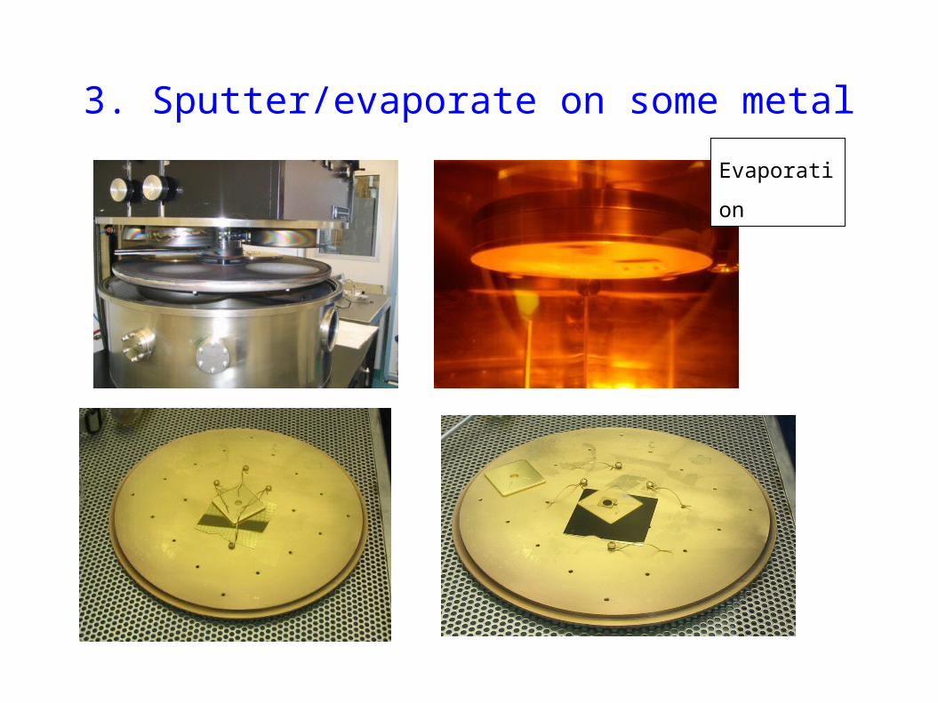
3. Sputter/evaporate on some metal
Evaporation
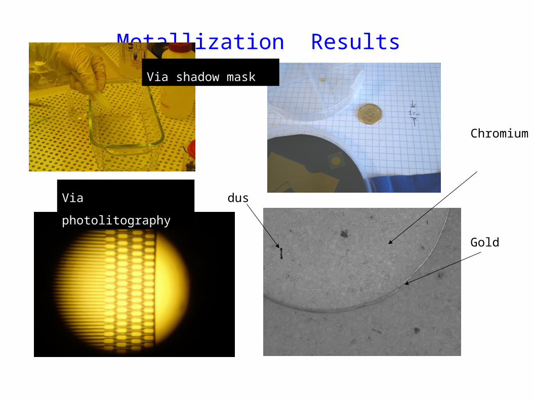
Metallization Results
dust
Chromium
Gold
Via photolitography
Via shadow mask
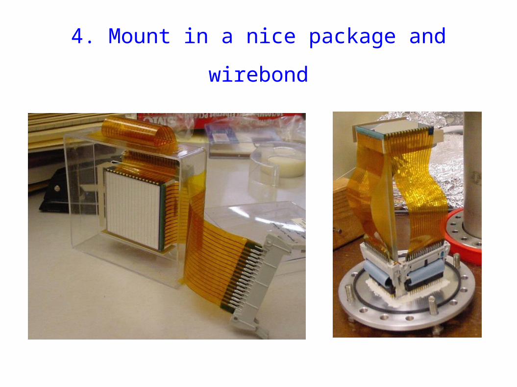
4. Mount in a nice package and wirebond
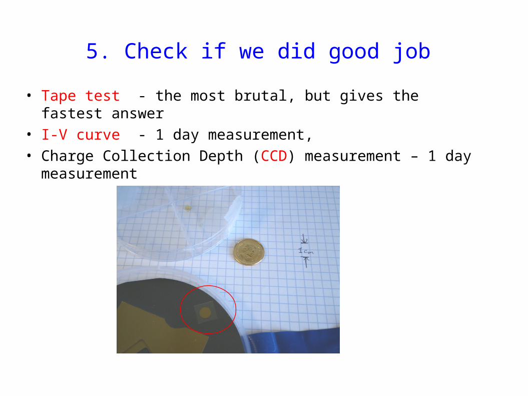
5. Check if we did good job
• Tape test - the most brutal, but gives the fastest answer• I-V curve - 1 day measurement,• Charge Collection Depth (CCD) measurement – 1 day
measurement
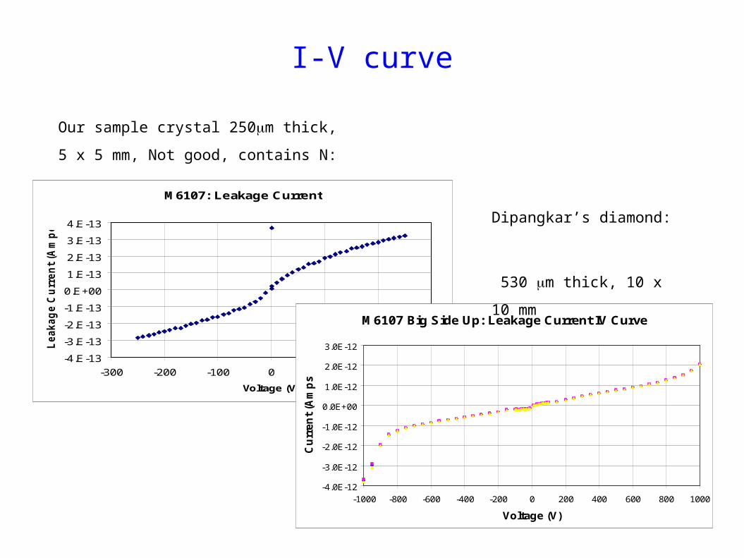
I-V curve
M6107: Leakage Current
-4.E-13
-3.E-13
-2.E-13
-1.E-13
0.E+00
1.E-13
2.E-13
3.E-13
4.E-13
-300 -200 -100 0 100 200 300
Voltage (V)
Leakag
e C
urr
en
t (A
mp
ere
s)
Our sample crystal 250m thick, 5 x 5 mm,
Not good, contains N:
M6107 Big Side Up: Leakage Current IV Curve
-4.0E-12
-3.0E-12
-2.0E-12
-1.0E-12
0.0E+00
1.0E-12
2.0E-12
3.0E-12
-1000 -800 -600 -400 -200 0 200 400 600 800 1000
Voltage (V)
Cu
rren
t (A
mp
s)
Dipangkar’s diamond:
530 m thick, 10 x 10 mm
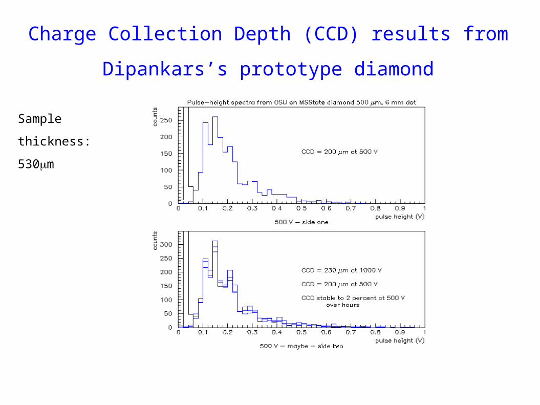
Charge Collection Depth (CCD) results from Dipankars’s
prototype diamond
Sample
thickness: 530m

Summary Coated f irs t test diamond at NSFL (University of Manitoba EE)
Visited Ohio State University (Harris Kagan group)
learned diamond preparation/metallizat ion in context of a second diamond (D. Dutta's)
learned mult i-strip detector fabricat ion
learned test procedures
CCD measurement
I-V curve
Coated third diamond (hopefully did it right) at NSFL