Embed Size (px)
Citation preview
Chapter 10
Dewetting Stability of ITO Surfaces in OrganicOptoelectronic Devices
Ayse Turak
Additional information is available at the end of the chapter
http://dx.doi.org/10.5772/52417
1. Introduction
Heterojunctions are inherent in and essential to all molecular optoelectronic devices. In or‐ganic light emitting diodes (OLEDs), the interfacial region between the active organic layersand the inorganic contacts plays a primary role in device performance, through the controlof effective carrier injection and long term device reliability. In organic solar cells (OPVs),heterojunctions play a defining role in all of the major processes: charge separation relies oneffective organic/organic interfaces; charge transport is critically determined by the structureof the thin film, controlled by the organic/inorganic interfaces with substrates; and chargeextraction can only occur at high quality inorganic/organic interfaces at the electrodes. Stud‐ies of various organic/inorganic interfaces have indicated that a wide range of interfacialtypes are possible in organic optoelectronic devices. To foster the next generation of devices,it is critical to understand the connections between heterojunction structure and morpholo‐gy, and device performance. This connection is especially important with regard to the inter‐facial stability and lifetime in organic optoelectronic devices. Control of the complexinteractions and the microstructure at the electrode-organic interfaces would allow the opti‐mization of performance and lifetime.
In this chapter, we aim to review the current state of the art with regards to interfacial stabil‐ity and control of the anode (indium tin oxide) electrode/active layer interfaces to under‐stand the performance of organic optoelectronic devices. From examples of our ownresearch and others relating to interfacial morphological changes, a comprehensive pictureof the role of the interface in device stability can be formed. This chapter begins with a briefoverview of degradation in organic devices, including definitions. Following that, the mainfocus of the chapter is on the morphological instability at the ITO surface as a main mecha‐nisms of device degradation. Various approaches to overcoming device instability are given,
© 2013 Turak; licensee InTech. This is an open access article distributed under the terms of the CreativeCommons Attribution License (http://creativecommons.org/licenses/by/3.0), which permits unrestricted use,distribution, and reproduction in any medium, provided the original work is properly cited.

with special attention paid to the various interlayers that have been introduced into devices.This also includes examples where dewetting is used advantageously to produce novel de‐vice architectures and surprising solutions to device degradation.
2. Degradation
Unlike the field of inorganic electronics, organic electronics encompasses highly diversetechnologies with devices that can be prepared with different architectures, using many dif‐ferent materials, processed by many different methods. Unlike their inorganic counterparts,all organic devices are to some extent unstable and their performance degrades over time[1]. After efficiency, lifetime is the second most important parameter for organic devices [2].While inorganic semiconductors are for the most part intrinsically chemically stable, and in‐sensitive to the ambient environment, for organic devices, the polymer or small molecule ac‐tive layers themselves, the inorganic electrodes, and the interfaces between them are allpotential locations for degradation. Degradation for organic devices is, therefore, highlycomplex and typically cannot be described by a single mechanism.
OLEDs [3] and OPVs [4-6] are known to degrade during both operation and storage (calledshelf life or dark stability). From the moment the metal electrode is applied, the device issubject to degradation: in vacuum, in the dark and under operation [1]. The three physicalmechanisms that degradation can take are the loss of conjugation and irreversible deteriora‐tion of the active organic layers; degradation of the interface conductive properties; and me‐chanical disintegration of device (dewetting, phase segregation, crystallization), all of whichmanifest themselves as a change in the electrical properties. The basic requirement of anemissive or absorptive technology with regards to lifetime is to provide adequate deviceperformance over the intended time of use for the application. Stability for short term dis‐plays, such as cell phone monitors, requires different criteria than long term high perform‐ance solid state lighting. For solar cells, the requirements are different still with exposure toexternal environments that are not even a consideration for OLEDs, aggravated by the factthat many organic molecules undergo serious degradation in electrical properties upon ex‐posure to light [7-11]. The desire for flexible substrates for both technologies brings yet an‐other set of challenges. These requirements have stimulated much research in the thirtyyears since the first OLEDs and OPVs were produced at Kodak [12-13].
Though efforts are underway to establish standardized protocols for OLED and OPV char‐acterization [14-16], official qualification procedures have not yet been established for life‐time testing. Stability testing protocols were proposed for OPVs by consensus among 21international research groups in May 2011 to improve the reliability of reported values [17],and are still in the process of being adopted by other researchers. A comparison of reportedlifetime values between different groups is difficult, as device lifetime is greatly affected bythe driving voltage, number of duty cycles, length of rest cycles, initial luminance or powerconversion efficiency, deposition conditions, and exposed environment. Though it is possi‐ble to estimate values for standardized test conditions using acceleration factors for both
Optoelectronics - Advanced Materials and Devices230
OLEDs [18] and OPVs [19-20], in general it is more instructive to look at the relative im‐provement in the device lifetime, which is how it will be discussed in this chapter.
Known degradation mechanisms include diffusion of molecular oxygen and water intothe device, crystallization or oxidation of organic layers, degradation of interfaces, inter‐layer and electrode diffusion, electrode reaction with the organic materials, electrode oxi‐dation, phase segregation or intermixing, dewetting from the substrate, delamination ofany layer, and the formation of particles, bubbles, and cracks. There are four major de‐cay mechanisms related to the bulk active layers: organic layer oxidation, crystallization,charge carrier/exciton damage, and photobleaching. There are also four decay mecha‐nisms directly associated with degradation at the top contact: electrode oxidation, darkspot formation, electrode bubbling and delamination, and metal diffusion. As this chap‐ter is focussed on the morphological stability on the anode surface, interested readers aredirected to recent topical reviews specifically focussed on polymer photovoltaics [21-22],on OLEDs [23], and on interfaces [24], for a comprehensive look at degradation and deg‐radation mechanisms. As many of the issues related to anodic degradation at interfacesare common for both OPV and OLEDS, and for polymer and small molecule active lay‐ers, all types will be discussed within this chapter.
3. Dewetting theory
It is the interplay between molecule-molecule self-interaction and substrate-molecule in‐teractions that determines the stability on a given surface [25-26]. For thin films (<100nm)coated onto non-wetting substrates, van der Waals forces play the dominant role in de‐termining film stability [27-28]. The Hamaker model [29] allows quantification of the in‐stabilities that arise in thin films when VdW forces induce an attractive potentialbetween two interfaces
2( )12
HAE h
hp-
= (1)
where AH is the effective Hamaker constant for the film and film-substrate interactions(AH=AF-AFS) and h is the film thickness on an infinite substrate.
The thermodynamic instability is given by the “disjoining pressure” [26, 30], or the secondderivative of the energy. For a single film, this is given by
2
2 4( )
2F FSA Ad E h
dh hp- +
= (2)
As the disjoining pressure is inversely proportional to the film thickness to the fourth pow‐er, producing stable and defect free films is particularly difficult as the thickness decreases.
Dewetting Stability of ITO Surfaces in Organic Optoelectronic Deviceshttp://dx.doi.org/10.5772/52417
231

At the lowest limits, thermally or mechanically induced fluctuations (capillary waves) tendto cause film rupture [27, 31-32], a process known as spinodal dewetting. The surface undu‐lations give rise to a pressure gradient which drives film instability if the effective Hamakerconstant is negative (i.e. non-wetting) [31]. As the film thickness decreases, there is a trade-off between destabilizing vdW forces and stabilizing surface tension that leads to an amplifi‐cation of capillary waves [33] and can therefore cause spontaneous rupture if the film is thinenough (typically <200nm, greatly enhanced at <10nm [32-33]). Additionally, the glass tran‐sition temperature (Tg) is lower for thin films due to confinement effects [34], further aggra‐vating dewetting effects. Most OLED and OPV layers are less than 200nm thickness, makingthem highly susceptible to spinodal dewetting.
Aside from capillary wave destabilization, dewetting can be driven by nucleation and holegrowth from defects (i.e. airborne particles) [27, 35], by the release of residual stress [36], bydensity variations [37] or by thermal expansion mismatch between substrate and organicfilm [27, 38], which can be highly anisotropic for organic molecules [39].
Dewetting effects are strongly related to the crystalline structure of organic thin films [40],and are thus quite different from the wetting – dewetting problems of an isotropic liquid.The situation is further complicated by the fact that many organic molecular crystals exhibitseveral distinct crystal structures, which are energetically very similar and may coexist[41-42]. For crystalline films, pseudo-epitaxy with the substrate can simultaneously driveboth film stabilization and dewetting [42]. The predominance of physisorption, combinedwith the relatively large size of the molecule compared to the inorganic substrate allows or‐ganic films to accommodate much larger strains than those observed in inorganic epitaxy[42]. As having lateral organization in the thin film can stabilize against dewetting [40], theamorphous films often used in devices are even more susceptible to extreme morphologicalinstabilities.
Regardless of the mechanism, dewetting begins with a nucleation event leading to the for‐mation of a hollow which proceeds to grow by the transport of material away from the nu‐cleation site to a retreating rim surrounding the hole. These holes eventually intersect,leading to the formation of ribbons of material along the contact line [27].
4. Anode/active layer contacts
The interface at the high work function electrode is especially influential in device stabilityas it often also forms the substrate upon which subsequent layers are deposited. The electri‐cal, chemical, and morphological features of the electrode surface play a significant role forboth OLEDs and OPVs as the quality of the interface and of the hole transporting (electrondonating) (HTL) film deposited on it [38, 43] is often the limiting feature of the device, bothfor performance [38, 44-47] and stability [9, 38, 48-50].
For a high quality device, the HTL needs to fulfill a number of criteria including high holemobility, good energy level matching with anodes and other active layers, good thermal
Optoelectronics - Advanced Materials and Devices232
properties, high optical transparency to visible light, and a smooth, often amorphous mor‐phology with good film forming properties [12, 51-59]. In small molecule OLEDs, excellentexamples, and the first HTL materials [12], are triphenylamines such as TPD and NPB; inpolymer OLEDS and OPVs, this function is often fulfilled by PEDOT:PSS (Poly(3,4-ethylene‐dioxythiophene):poly(styrenesulfonate)) [60].
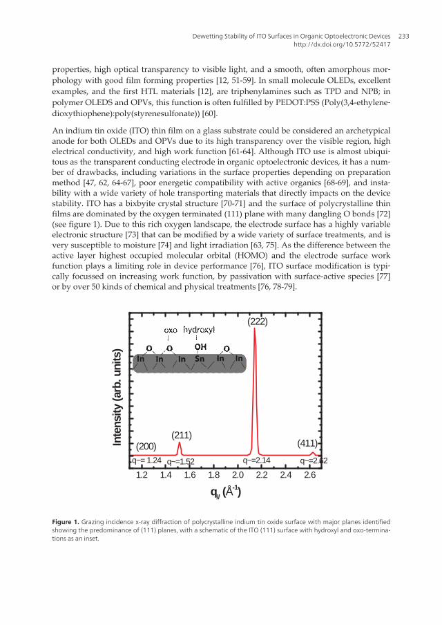
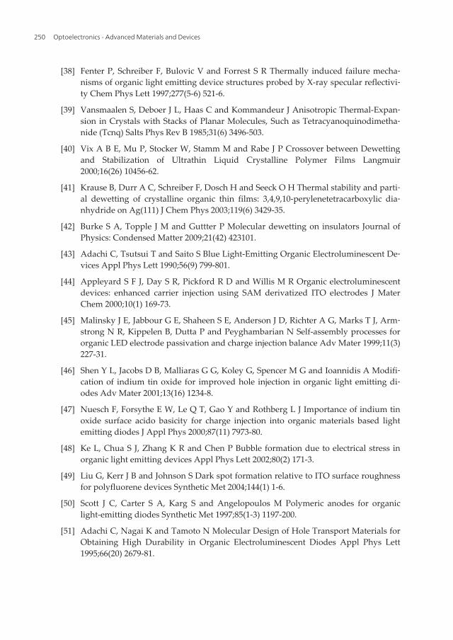
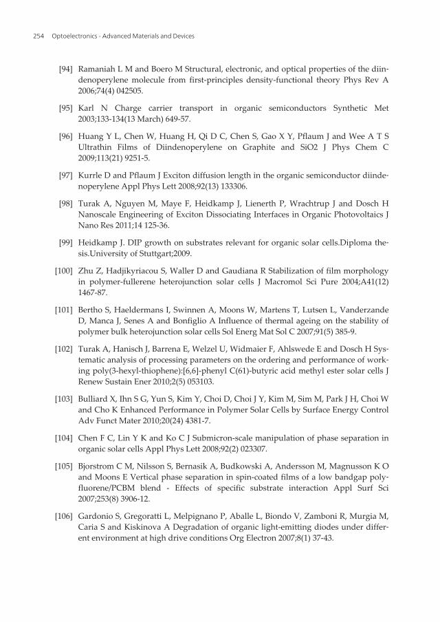
An indium tin oxide (ITO) thin film on a glass substrate could be considered an archetypicalanode for both OLEDs and OPVs due to its high transparency over the visible region, highelectrical conductivity, and high work function [61-64]. Although ITO use is almost ubiqui‐tous as the transparent conducting electrode in organic optoelectronic devices, it has a num‐ber of drawbacks, including variations in the surface properties depending on preparationmethod [47, 62, 64-67], poor energetic compatibility with active organics [68-69], and insta‐bility with a wide variety of hole transporting materials that directly impacts on the devicestability. ITO has a bixbyite crystal structure [70-71] and the surface of polycrystalline thinfilms are dominated by the oxygen terminated (111) plane with many dangling O bonds [72](see figure 1). Due to this rich oxygen landscape, the electrode surface has a highly variableelectronic structure [73] that can be modified by a wide variety of surface treatments, and isvery susceptible to moisture [74] and light irradiation [63, 75]. As the difference between theactive layer highest occupied molecular orbital (HOMO) and the electrode surface workfunction plays a limiting role in device performance [76], ITO surface modification is typi‐cally focussed on increasing work function, by passivation with surface-active species [77]or by over 50 kinds of chemical and physical treatments [76, 78-79].
1.2 1.4 1.6 1.8 2.0 2.2 2.4 2.6
Inte
nsity
(arb
. uni
ts)
q// (Å-1)
(200)q~= 1.24
(211)
q~=1.52
(222)
q~=2.14
(411)
q~=2.62
Figure 1. Grazing incidence x-ray diffraction of polycrystalline indium tin oxide surface with major planes identifiedshowing the predominance of (111) planes, with a schematic of the ITO (111) surface with hydroxyl and oxo-termina‐tions as an inset.
Dewetting Stability of ITO Surfaces in Organic Optoelectronic Deviceshttp://dx.doi.org/10.5772/52417
233

5. Morphological instabilities on ITO
In general, instability at the ITO/active layer interface can be related to morphological,chemical and electronic changes over the lifetime of the device. There are four major criteriawhich lead to an unstable interface: surface energy mismatch, low glass transition tempera‐ture (Tg) materials, surface reactivity with organics, and work function instability. The sur‐face energy mismatch and low transition temperatures are the driving characteristics for themorphological instability discussed in this chapter.
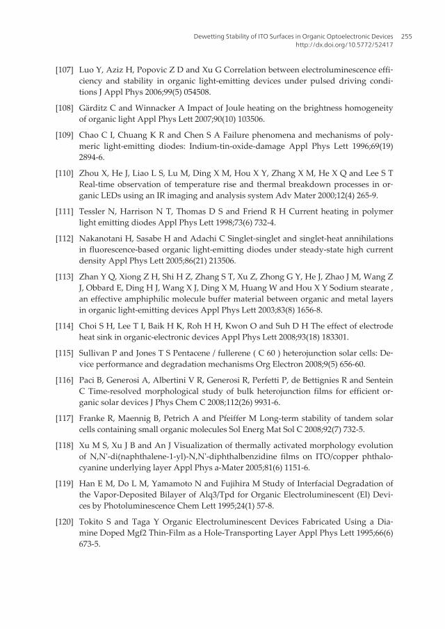
As the ITO surface consists of many dangling O, surface treatments tend to saturate the sur‐face with hydroxides, making it hydrophilic [80]. Advancing aqueous contact angles rangefrom ~0-30o on treated surfaces [80-86]. By contrast, many electron donating organic materi‐als are hydrophobic. Two widely used HTLs for small molecule OLEDs, TPD and NPB, haveadvancing contact angles of 80°, and 90° respectively [80]. This large mismatch in surface en‐ergy makes it difficult to grow continuous films necessary for devices. Thermally evaporat‐ed oligomers, such as NPB [87-88] and TPD [89] as well as many others, show a strongtendency to island (Volmer-Weber) growth (see figure 2a), with highly active surface diffu‐sion to step edges and defects. Often, the initially formed islands can ripen laterally withcontinued deposition to form what appear to be continuous films [87], which are highlymetastable. For molecules deposited from solution, the surface energy mismatch with ITOcan also lead to inhomogenous deposition, as seen in figure 2b for PEDOT:PSS.
Even when continuous films are able to form upon deposition, the relatively low Tg formany oligomer hole transporting materials (NPB 96oC, TPD 65oC [53]), can lead to dewet‐ting under mild thermal treatments or even with storage over time at ambient temperatures[42, 90]. Diindenoperylene, a novel material of interest due to its well defined ordering [91],interesting growth behaviour [92-93], promising electron transport properties [94-95], fa‐vourable electronic structure [96], long exciton diffusion lengths [97], has recently beenshown by us to have tuneable behaviour in solar cells based on its morphology [98]. As seenin figure 3, upon initial deposition, films of DIP form large flat islands on ITO with a high
(a)
(b)
Figure 2. (a) SEM image of (EtCz)2 films deposited at Ts = 90oC on a bare-ITO substrate. Reprinted with permissionfrom [68]. Copyright 2002 John Wiley and Sons (b) Incomplete coverage of ITO surface with PEDOT:PSS depositedfrom solution.
Optoelectronics - Advanced Materials and Devices234
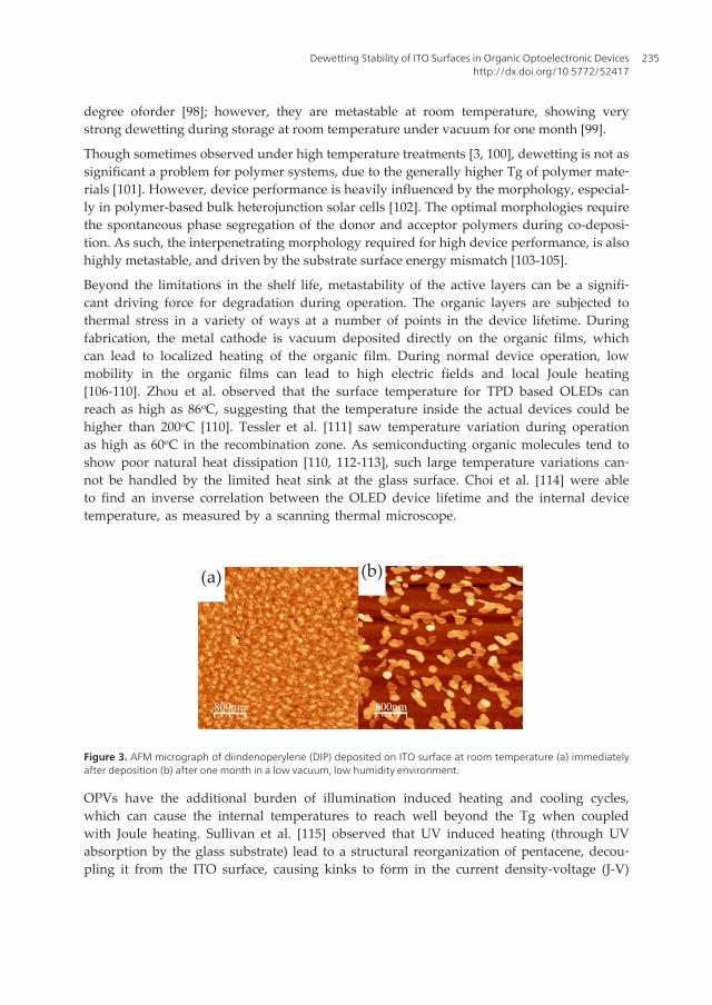
degree oforder [98]; however, they are metastable at room temperature, showing verystrong dewetting during storage at room temperature under vacuum for one month [99].
Though sometimes observed under high temperature treatments [3, 100], dewetting is not assignificant a problem for polymer systems, due to the generally higher Tg of polymer mate‐rials [101]. However, device performance is heavily influenced by the morphology, especial‐ly in polymer-based bulk heterojunction solar cells [102]. The optimal morphologies requirethe spontaneous phase segregation of the donor and acceptor polymers during co-deposi‐tion. As such, the interpenetrating morphology required for high device performance, is alsohighly metastable, and driven by the substrate surface energy mismatch [103-105].
Beyond the limitations in the shelf life, metastability of the active layers can be a signifi‐cant driving force for degradation during operation. The organic layers are subjected tothermal stress in a variety of ways at a number of points in the device lifetime. Duringfabrication, the metal cathode is vacuum deposited directly on the organic films, whichcan lead to localized heating of the organic film. During normal device operation, lowmobility in the organic films can lead to high electric fields and local Joule heating[106-110]. Zhou et al. observed that the surface temperature for TPD based OLEDs canreach as high as 86oC, suggesting that the temperature inside the actual devices could behigher than 200oC [110]. Tessler et al. [111] saw temperature variation during operationas high as 60oC in the recombination zone. As semiconducting organic molecules tend toshow poor natural heat dissipation [110, 112-113], such large temperature variations can‐not be handled by the limited heat sink at the glass surface. Choi et al. [114] were ableto find an inverse correlation between the OLED device lifetime and the internal devicetemperature, as measured by a scanning thermal microscope.
800nm 800nm
(a) (b)
Figure 3. AFM micrograph of diindenoperylene (DIP) deposited on ITO surface at room temperature (a) immediatelyafter deposition (b) after one month in a low vacuum, low humidity environment.
OPVs have the additional burden of illumination induced heating and cooling cycles,which can cause the internal temperatures to reach well beyond the Tg when coupledwith Joule heating. Sullivan et al. [115] observed that UV induced heating (through UVabsorption by the glass substrate) lead to a structural reorganization of pentacene, decou‐pling it from the ITO surface, causing kinks to form in the current density-voltage (J-V)
Dewetting Stability of ITO Surfaces in Organic Optoelectronic Deviceshttp://dx.doi.org/10.5772/52417
235
curves for PEN:C60 solar cells. Paci et al. [116] observed that the metastable morphologyof P3HT:PCBM solar cells was modified in a similar way under illumination as by delib‐erate thermal annealing.
Irreversible device failure has also been observed in operating OLEDs [38] and OPVs [117]heated above Tg of one of the molecular organic components. For many devices, the weak‐est link in the device lifetime is the low Tg of the HTL immediately adjacent to the ITO sur‐face [117-121], as many electron accepting and transporting materials have relatively highTg [53]. Fenter et al. proposed that device failure was a result of significant expansion of theleast thermally stable material, TPD, leading to delamination from the ITO surface [38]. Doet al. for MEH-PPV [3] and Choi et al [114] for PFO, observed buckling behaviour, where thepolymer layer completely detached from the ITO in a number of areas on the electrode sur‐face. This inhomogenous delamination results in significant disruption of the multilayerstructure, which can cause non-uniform contact between the electrode and organic layers.TPD undergoes signifcant structural changes even well below its glass transition tempera‐ture: at ~60oC, changes have been observed in its thickness and density by XRR [38] and seri‐ous dewetting has been observed by AFM [122]. Tokito et al. [123] observed a directcorrelation between the glass transition temperature of the HTL and device degradation as afunction of temperature; however, this was disputed by Adachi et al. [51], who saw no cor‐relation specifically with the Tg, relating the stability more to the interfacial barrier to injec‐tion (and hence to Joule heating [124]). It is conceivable that dewetting, which compromisesthe integrity of the hole transport layer, would lead to inefficient hole injection by non-uni‐form coverage, and a modification of the other layers deposited atop the dewetted layer[125].
Any local failures due to morphological inhomogeneities on the ITO surface (In spikes, thin‐ner organic regions, etc) [90], where the high local electric field would already encourageJoule heating, would also tend to both accelerate and be accelerated by dewetting. As manymaterials are also subject to annealing heat treatments for improved performance, film met‐astability can have catastrophic consequences for the device in operation. Do et al. observedcomplete separation of the active MEH-PPV layer during operation in a number of areas onthe electrode surface, resulting in dead areas that eventually covered the whole surface [3].Even without dewetting induced failures, over-annealing or elevated temperature storageover long time can lead to significant phase-segregation beyond the exciton diffusion lengthfor bulk heterojunction devices [126-128], which ultimately decreases the performance overtime [101, 127, 129-130].
Both dewetting and work function instability at ITO surfaces are accelerated by humidity[86, 90] or light irradiation [115-116]. The same mechanism is at work in both cases – themodification of the hydroxyl termination on the ITO surface [47], which leads to a change inthe surface energy. This also helps to explain the strong correlation observed between theinterfacial barrier to hole injection and OLED device degradation [51, 131-133], as both arerelated to this hydroxyl terminated surface.
Optoelectronics - Advanced Materials and Devices236

6. Preventing interfacial morphological instability
There has been much research into methods of counter-acting dewetting from the ITO sur‐face, as the integrity of the active layers is of paramount importance in the device perform‐ance and stability. Incorporation of the unstable film into a device, with a mutli-layer filmstack, already significantly suppresses the dewetting of single films [40, 125, 134]. Deliberateuse of a stable inorganic capping layer, such as Al2O3 [135] or an electrode metal such as Ag[136] or Au [137], within the device can also greatly improve the stability of the underlyingorganic phases. Utilizing a rough substrate can also encourage wetting and stability [32, 46,138-140], but that can lead to undesirable morphologies in the original deposition [99]. In or‐der to further improve the stability at the ITO surface, two general approaches have beenadopted: increasing the Tg of the active layer itself, or introducing stabilizing interlayers.
6.1. Increasing the glass transition temperature
There has been much work over the last 30 years focused on finding new hole transporting/electron donating molecules that have high morphological stability, as recently reviewed byShirota [56]. General strategies for designing morphologically stable molecules were devel‐oped by Shirota [55-56], Wirth [141] and Naito and Muira [53] -- the underlying philosophywas to decrease the degrees of freedom and increase the rigidity of the molecules, throughreplacement/augmentation of the core; linear or branch linkages; or long substituents lead‐ing to starbust type molecules. The first and most widely used replacement of the originaltriphenyldiamine used in the Tang OLED (TPD) [12], was a benzedine derivative, NPB. Ithad excellent hole transporting and film forming properties in addition to a slightly higherTg (~96oC) [133, 142-143]. Though NPB was widely adopted in OLEDs, unfortunately it toohad a propensity to crystallization and dewetting albeit at higher temperatures [118, 144].The original family of triphenyldiamines were successful in most other aspects as a holetransporting layer leading to the development of various derivatives, including triphenylamines [120, 123], biphenyl amines [142], binaphlathene diamines [145], asymmetric triaryl‐diamines (TPD derivatives) [146], triphenylamine-based starburst molecules [147-149], andrecently star-shaped oligotriarylamines [150]. Other approaches include using a fluorenecore to increase the rigidity of biphenyl HTLs [121], carbazole derivatives [151], vinyl-typepolynorborenes with ethyl ester linked triarylamines [152], thermoclevable densified poly‐mers [153-154], defect reduced polymers [130, 155-156], among many others. Though newmaterials are synthesized regularly with significantly higher glass transition temperaturesthan the classically utilized molecules, the correct combination of high hole mobility, goodenergetic compatibility with electron-accepting materials, and good optical absorbance hasproven elusive, and many of these materials currently do not see widespread use in devices.
6.2. Interfacial structure stabilizing interlayers
Due to the difficulties in finding complete replacements to traditional hole transport/elec‐tron donating layers, much research has gone into introducing thin adhesion-promotingbuffer layers between the active material and the ITO anode. The ideal interlayer should ex‐
Dewetting Stability of ITO Surfaces in Organic Optoelectronic Deviceshttp://dx.doi.org/10.5772/52417
237
hibit strong adhesion to both the anode and the HTL, via physical adhesion or chemicalbonds. Other desirable criteria for an effective buffer should include (1) high hole transportmobility; (2) easy deposition onto anode surfaces via straight-forward methods such as spin-coating, vapor-deposition, or self-assembly; (3) good conformal matching to substrate; (4)substantial thickness control; and (5) well-defined microstructure free of pinhole defects.
In addition to promoting adhesion and stabilizing against dewetting, buffer layers oftenhave a number of added benefits for the device, including enhancing initial device perform‐ance [81, 86, 133, 157-167], encouraging better charge balance [45, 168-169] (often by prevent‐ing hole injection [131]), preventing chemical reactions between the active layer and ITO [9,162, 170-172], blocking In and Sn diffusion [170, 173-176], increasing mechanical strength[177], and smoothing the ITO surface (preventing electric field inhomogeneities that are po‐tentially responsible for dark spot formation) [64, 161-162, 171, 175-176, 178-180].
There are two broad classes of interlayers that have been used to suppress dewettingspecifically, or device degradation more broadly: modifications of HTLs (covalentlybound or polymerized versions of traditional hole transport layers; HTL materials dopedwith or into a stabilizing material); and any organic, metal or oxide buffer that is not al‐so used as the HTL.
6.2.1. Generic buffer layers
The most widely explored class is that of generic buffer layers. These run the gamut fromvapor or solution deposited organic layers, self-assembled monolayers, dielectrics, conduct‐ing oxides, insulating oxides, to metals. Virtually every element in the periodic table hasbeen incorporated into the device with the aim of increasing the device lifetime. A wide va‐riety of interlayers have also been introduced with no interest in their stabilizing properties,though film stability often also results as a side effect. These interlayers include metal dopedITO [181-183]; oxides including Y2O3 [184], Tb4O7 [184], TiO2 [184-185], ZnO [184], Nb2O3
[184], Ga2O3 [184], SnO2 [184], CuOx [186], Fe2O3 [187], SiO2 [188], VOx [189-190], RuOx [189],AZO [189], Al2O3 [191], NiO [192]; ultrathin metal layers such as Ni [184], Au [184], Sn [184],Pb [184]; F16CuPc [193]; conducting polymers [194]; and a wide variety of self-assembledmonolayers [44-45, 195]. While this is not an exhaustive list, it demonstrates that a wide vari‐ety of buffer layers have been attempted by researchers. The focus for the rest of this sectionwill be on interlayers that are specifically shown to influence the device lifetime or stabilityof the organic layers deposited on the surface. The reported improvements in device lifetimefor a variety of interlayers are summarized in table 1.
One of the first and still most widely used buffer layer for small molecule OLEDs is copperphthalocyanine (CuPc). Though an interesting semiconducting material in its own right[196-199] with current widespread use in solar cells as an electron donating material [200], itwas first introduced as a stabilizing buffer layer for NPB [133]. It has been extensively em‐ployed as an anode HTL buffer layer, mostly due to its reported ability to enhance OLEDperformance [44, 132-133, 164, 201-202], energetic level matching [203-205], high thermal sta‐bility [204, 206], and low cost as a result of its use as a blue dye [207]. Other phthalocyanineshave also been employed as buffer layers below the active layers [207]; the recent use of
Optoelectronics - Advanced Materials and Devices238
ZnPc [63], for example, improved the stability of ZnPc:C60 bulk heterojunction solar cells by~3.5x (see table 1).
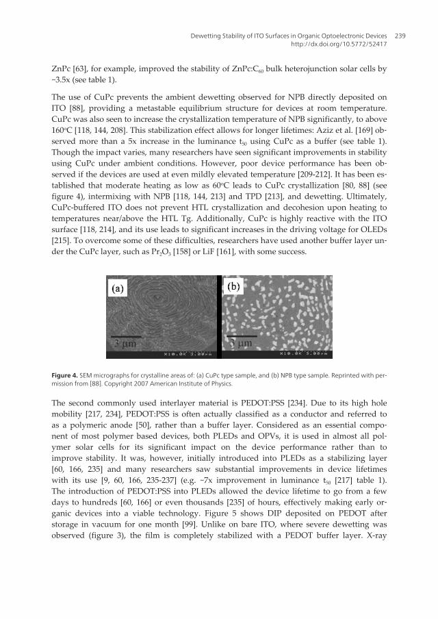
The use of CuPc prevents the ambient dewetting observed for NPB directly deposited onITO [88], providing a metastable equilibrium structure for devices at room temperature.CuPc was also seen to increase the crystallization temperature of NPB significantly, to above160oC [118, 144, 208]. This stabilization effect allows for longer lifetimes: Aziz et al. [169] ob‐served more than a 5x increase in the luminance t50 using CuPc as a buffer (see table 1).Though the impact varies, many researchers have seen significant improvements in stabilityusing CuPc under ambient conditions. However, poor device performance has been ob‐served if the devices are used at even mildly elevated temperature [209-212]. It has been es‐tablished that moderate heating as low as 60oC leads to CuPc crystallization [80, 88] (seefigure 4), intermixing with NPB [118, 144, 213] and TPD [213], and dewetting. Ultimately,CuPc-buffered ITO does not prevent HTL crystallization and decohesion upon heating totemperatures near/above the HTL Tg. Additionally, CuPc is highly reactive with the ITOsurface [118, 214], and its use leads to significant increases in the driving voltage for OLEDs[215]. To overcome some of these difficulties, researchers have used another buffer layer un‐der the CuPc layer, such as Pr2O3 [158] or LiF [161], with some success.
Figure 4. SEM micrographs for crystalline areas of: (a) CuPc type sample, and (b) NPB type sample. Reprinted with per‐mission from [88]. Copyright 2007 American Institute of Physics.
The second commonly used interlayer material is PEDOT:PSS [234]. Due to its high holemobility [217, 234], PEDOT:PSS is often actually classified as a conductor and referred toas a polymeric anode [50], rather than a buffer layer. Considered as an essential compo‐nent of most polymer based devices, both PLEDs and OPVs, it is used in almost all pol‐ymer solar cells for its significant impact on the device performance rather than toimprove stability. It was, however, initially introduced into PLEDs as a stabilizing layer[60, 166, 235] and many researchers saw substantial improvements in device lifetimeswith its use [9, 60, 166, 235-237] (e.g. ~7x improvement in luminance t50 [217] table 1).The introduction of PEDOT:PSS into PLEDs allowed the device lifetime to go from a fewdays to hundreds [60, 166] or even thousands [235] of hours, effectively making early or‐ganic devices into a viable technology. Figure 5 shows DIP deposited on PEDOT afterstorage in vacuum for one month [99]. Unlike on bare ITO, where severe dewetting wasobserved (figure 3), the film is completely stabilized with a PEDOT buffer layer. X-ray
Dewetting Stability of ITO Surfaces in Organic Optoelectronic Deviceshttp://dx.doi.org/10.5772/52417
239
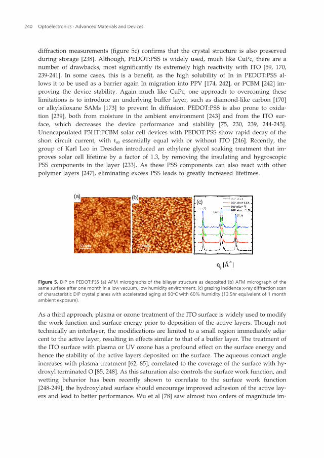
diffraction measurements (figure 5c) confirms that the crystal structure is also preservedduring storage [238]. Although, PEDOT:PSS is widely used, much like CuPc, there are anumber of drawbacks, most significantly its extremely high reactivity with ITO [59, 170,239-241]. In some cases, this is a benefit, as the high solubility of In in PEDOT:PSS al‐lows it to be used as a barrier again In migration into PPV [174, 242], or PCBM [242] im‐proving the device stability. Again much like CuPc, one approach to overcoming theselimitations is to introduce an underlying buffer layer, such as diamond-like carbon [170]or alkylsiloxane SAMs [173] to prevent In diffusion. PEDOT:PSS is also prone to oxida‐tion [239], both from moisture in the ambient environment [243] and from the ITO sur‐face, which decreases the device performance and stability [75, 230, 239, 244-245].Unencapsulated P3HT:PCBM solar cell devices with PEDOT:PSS show rapid decay of theshort circuit current, with t80 essentially equal with or without ITO [246]. Recently, thegroup of Karl Leo in Dresden introduced an ethylene glycol soaking treatment that im‐proves solar cell lifetime by a factor of 1.3, by removing the insulating and hygroscopicPSS components in the layer [233]. As these PSS components can also react with otherpolymer layers [247], eliminating excess PSS leads to greatly increased lifetimes.
(c)(a) (b)
Figure 5. DIP on PEDOT:PSS (a) AFM micrographs of the bilayer structure as deposited (b) AFM micrograph of thesame surface after one month in a low vacuum, low humidity environment. (c) grazing incidence x-ray diffraction scanof characteristic DIP crystal planes with accelerated aging at 90oC with 60% humidity (13.5hr equivalent of 1 monthambient exposure).
As a third approach, plasma or ozone treatment of the ITO surface is widely used to modifythe work function and surface energy prior to deposition of the active layers. Though nottechnically an interlayer, the modifications are limited to a small region immediately adja‐cent to the active layer, resulting in effects similar to that of a buffer layer. The treatment ofthe ITO surface with plasma or UV ozone has a profound effect on the surface energy andhence the stability of the active layers deposited on the surface. The aqueous contact angleincreases with plasma treatment [62, 85], correlated to the coverage of the surface with hy‐droxyl terminated O [85, 248]. As this saturation also controls the surface work function, andwetting behavior has been recently shown to correlate to the surface work function[248-249], the hydroxylated surface should encourage improved adhesion of the active lay‐ers and lead to better performance. Wu et al [78] saw almost two orders of magnitude im‐
Optoelectronics - Advanced Materials and Devices240

provements in t50 with plasma treatments. Not all plasma treatments lead to the sameresponse, however. The study by Huang et al [67] showed that the wettability of NPB is in‐creased by H2, CF4 and O2 plasmas, but decreases with Ar plasma. They suggested that de‐contamination of the surface without hydroxylation leads to a dipole field on the surfacethat is stronger than the grain boundary and defect effects, promoting NPB nucleation. Onthe other hand, CF4 and O2 strongly encourage layer-by-layer growth, smoothing [219] andpassivating the surface against defects that can lead to inhomogeneous electric fields. As aninteresting aside, the results for UV-ozone treatment of the ITO surface by Fukushi et al[220] contradict the above. They saw ~5-6x improvement in t50 with a treatment that de‐creased the aqueous contact angle to 4o. They speculate that stronger adhesion of the HTLwas possible, which contradicts thermodynamic wetting theory as the surface energy mis‐match would be incredibly large. This underscores the likelihood that, as with many aspectsof organic semiconductors, more than one mechanism is responsible for lifetime improve‐ments in devices.
Silane based SAMs, such as tetraaryldiamine (TAA) [80, 213, 250], epoxysilane functional‐ized triphenylamine (TPA-silane) [81], dodecyltrichlorosilane (DDTS) [82], phenyltriethox‐ysilane (PTES) [82], 3-aminopropyl-methyl-diethoxysilane (APMDS) [82], alkylsiloxane[173], and alkytrichlorosilanes (OTCS and FOTCS) [83] use a Si-O bond to anchor on theITO surface, providing a robust interface with substantially higher surface energy. Chonget al [82] observed that the sticking and dewetting of NPB on various SAMs shows aninverse correlation with the measured aqueous contact angle, but Choi et al saw substan‐tially longer lifetimes (x11 increase in t50 with 105o contact angle on FOTCS [83]). The im‐proved adhesion of the active layer was attributed to interfacial reconstruction andinterpenetration with the SAM [251]. Our recent study of quaterrylene molecules onSAM buffered surfaces showed a significant release of interfacial strain when the bufferwas present [252]. As strain release is another mechanism that drives dewetting [36], bet‐ter pseudo-epitaxial conformation with the surface for buffered films could be a mecha‐nism for the observed improvement in performance.
A wide variety of other organic molecular interlayers have been used, with varying successin improving the lifetime, as summarized in table 1. These include oligomers such as 4,4’,4’’-(3-methylphenyl-phenylamino)triphenylamine (MTDATA) [147, 178, 253], parylene [162,175, 254], cross-linked perylenediimide (PDMI) [255], N,N-bis(4-trifluoromethoxyben‐zyl)-1,4,5,8-naphthalene-tetracarboxylic diimide (NTCDI-OCF3) [159], Alq3, or fullerene(C60). Most of these interlayers are thought to improve the active layer film formation on thesurface, by smoothing [147, 162, 180, 255]. The high Tg of MTDATA [253] and NTCDI-OCF3
[159] are also thought to contribute to preventing crystallization of the HTL overlayer. Poly‐mer approaches include polyanaline (PAni) [172], fluoropolymer (FC-227) [179], plasmapolymerized fluorocarbons [74, 160], tetrahedral amorphous carbon [171], polyimide [176]or radical ion salt doped amine polymer [221], which are thought to prevent oxidation [74,160, 172] or block hole injection [221], in addition to stabilizing the surface against dewetting
Metals such as Pt and Mg have also been used as interlayers, and though both show im‐provements, the mechanisms are almost completely opposed. High work function Pt enhan‐
Dewetting Stability of ITO Surfaces in Organic Optoelectronic Deviceshttp://dx.doi.org/10.5772/52417
241
ces TPD wetting on ITO surfaces [46], while low work function materials such as Mg, Caand Al give many orders of magnitude improvement in the luminance stability, correlatedto the work function of the metal, by preventing the injection of holes into the Alq layer inOLEDs (intrinsic degradation) [169].
Most recently, MoOx has been successfully employed to improve lifetimes in both OLEDs[157, 218] and OPVs [75, 230-232], especially as a replacement for PEDOT:PSS, and thoughthe mechanism is still controversial, the energy barrier at the active layer/ITO interface isthought to play a significant role. Other oxides, such as SiOxNy [86] or ZnO [256], which canact as oxygen and moisture getters, have been successfully used to stabilize the ITO surfaceagainst contamination.
6.2.2. Modified HTLs
There are three modifications that have been made to the hole transporting/electron donat‐ing layer adjacent to the ITO surface to improve its wetting properties: doping, polymeriza‐tion, and functionalization to allow for covalent bonding to the surface. Though many of thelayers discussed in this section have also been tried as the HTL for a given device structure,they have found more success for high device performance coupled with stability when theyare used as an ultra-thin buffer layer beneath the unmodified version of the molecule actingas the HTL.
Doping
The first approach to stabilization is through doping, either with nanoparticles or with othermolecules. Doping with other molecules, often referred to as alloying or more recently as abulk heterojunction, has been very successful in suppressing crystallization and dewettingin hole transporting molecules [131, 159, 169, 206, 225-227, 257-258]. Mori et al. used metal-free Pc to disrupt the crystallization of CuPc, showing ~2x improvement in lifetimes for op‐eration above 85oC [206]. Chu et al. [159] and Lee et al. [227] used higher stability moleculesNTCDI (diimide) and PFI (perfluorinatedionomer) to stabilize NPB and PEDOT:PSS, respec‐tively. The incorporation of PCBM into various polymers, including P3HT [100, 259], PPV,MDMO:PPV [260], also stabilizes the morphology against heat treatment, and improveslong-term stability [100, 259-260]. Addition of a diblock co-polymer of P3HT-C60 to aP3HT:PCBM composite has led to even greater stabilization against phase desegregation[261-262]. In some cases, the hole transport molecule was doped into a more stable matrix,such as TPD into high Tg polymers [263] or MgF2 [120], which significantly suppressed thecrystallization. Ruberene:TPD [257], MADN:NPB [226], F4TCNQ:NPB [131, 169],DSA_Ph:NPB [225]) combinations have all been employed with various levels of doping,leading in most cases to ~2x improvement in the 80% luminance lifetime in small moleculeOLEDs (see table 2). One very successful method of improving device stability has beendoping of the Alq3 layer in small molecule OLEDs with other molecules including TPD[258], NPB [210], NPD [218], quadricone [209], styrlamine [225], DMQA [264], rubrene [257,265], DNP [266], Bphen [267], perylene [265-266], among many others [265]. This approach,however, is focused on combating the intrinsic degradation of Alq3 by holes [168]. Thismechanism, hole blocking, was also suggested as an additional mechanism for a few of the
Optoelectronics - Advanced Materials and Devices242
doped hole transport layers (MADN:NPB [226], F4TCNQ:NPB [131, 169], DSA_Ph:NPB[225], Ir(piq)3:NPD [268]). As the focus of this section is on the stabilization at the ITO sur‐face, the summary in table 1 has been limited to doping in the HTL.
Doping with nanoparticles (LiF [88], C60 [32, 88, 269-271], NaCl [215], Au [33]) has also beenvery successful in stabilizing hole transport layers, though there is sometimes a trade-off be‐tween stability and performance for such systems [88]. As particulates in the layer can act asnucleation centres for crystallization [272-273], care must be taken when selecting doping pa‐rameters. The concentration and layer thickness must be chosen such that the electrical per‐formance is not adversely affected by the presence of the doped layer. Interparticle or surfaceforces strongly influence suspension behaviour of nanoparticles; therefore, not every nanofil‐ler works with every organic. We observed that LiF greatly enhances the stability of NPB at120oC, while having no impact on the crystallization of CuPc [88]. There is a long history ofnanoparticle inclusions for stabilization in non-conducting polymers [32, 274-275]. Luoet al.[275] suggests that a combination of factors are responsible for the stabilization effects, such asthe mobility of nanofillers, their size, interaction with the organic, and additional pinning ef‐fects at contact lines. Fillers work best if they are immobile; therefore, diffusion to and pinningat the substrate interface is one suggested mechanism for stabilization [32, 274]. Chu et al.[222] did in fact see similar improvement in stability with a C60 layer deposited at the interfacebelow NPB as Yuan et al. [270] saw with doping C60 into NPB; Barnes et al. [32], however, sawgreatly enhanced dewetting with C60 at the Si surface for polystyrene thin films. Additionally,there are a number of cases where diffusion to the substrate is unlikely, as no phase separationwas observed [88, 120, 215] even though stability was improved. Mukherjee et al. [33] recentlyobserved a concentration dependence on the stabilization, where dewetting droplets form acore-shell structure, rather than leaving behind nanoparticles as the polymer layer retreats aswould be expected for substrate segregation. In such cases, strong electrostatic or charge-transfer interactions between the particle and the organic layer leading to a cross-linked net‐work are the most likely route to highly stable films [88, 274]. Other possible mechanisms forstabilization include changing the Tg with high volume-surface area ratio (effectively modify‐ing the film rheology), preventing heterogeneous nucleation, and relief of residual stress inthe film through de-segregation [33].
Functionalized HTL
Another approach to stabilization, spearheaded by Tobin Marks’ at Northwestern University[45, 80, 163-164, 213, 250, 276-278], focuses on functionalizing traditional hole transport mate‐rials with siloxane groups. This allows the molecules to covalently bond to the ITO surfacethrough the formation of Si-O bonds (see figure 6) in a manner similar to the SAMs discussedin section 5.2.1. Covalent bonds ensure strong adhesion and directly eliminate the surface en‐ergy mismatch [84, 163]. As the interlayer is the same molecule as the HTL, deposition contin‐ues in a self-epitaxial fashion, yielding uniform films as large as 25μm2 without cracks orpinholes [163]. Aqueous contact angles of 90° compared to 110° for the active layer ensuresgood wetting and physical cohesion in MDMO-PPV:PCBM bulk heterojunction solar cells[277-278] with dewetting prevention above 60oC. Typical examples include TPD-Si2 [80, 163,213, 276-277], NPB-Si2 [80, 163, 279], PABT-Si2 [278], penta(organo)fullerenes [84] (which use
Dewetting Stability of ITO Surfaces in Organic Optoelectronic Deviceshttp://dx.doi.org/10.5772/52417
243
phosphonic acid linkages [72] rather than silane), and fluorinated triphenyldiamine (FTPD)[280]. An additional step of thermal curing leads to a cross-linked siloxane network, resultingin thin layer with HTL characteristics covalently anchored on surface [163, 280].
Polymerized HTL
The final widely used method of increasing the stability of the active layer on the ITO sur‐face requires a crosslinked polymer or highly crystallized version of a traditional HTL as aninterlayer [55, 143, 146, 280-283]. This approach has been most commonly applied to TPD[55, 146, 280-282], where significant stabilization was observed above 80oC with polymeriza‐tion. Bellman et al also observed that the voltage increase with time for small moleculeOLEDs was slower compared to those without the crosslinked interlayer [280], suggestingincreased stability. In-situ polymerization/crystallization, by heat treatment or high temper‐ature deposition (NPB [143, 284]) or by UV irradiation (TPD [282]), lead to significant in‐creases in the shelf life (>2 months for NPB), and operational stability at high temperatures.This approach has also been applied to polymers, where the most common approach is touse a heat-treatment [228-229, 285](already widely used in solar cells to improve efficiency[102]), with as much as two orders of magnitude improvement in lifetime [229]. Some suc‐cess has also be observed for doping and irradiation induced polymerization, mainly withPEDOT:PSS [286].
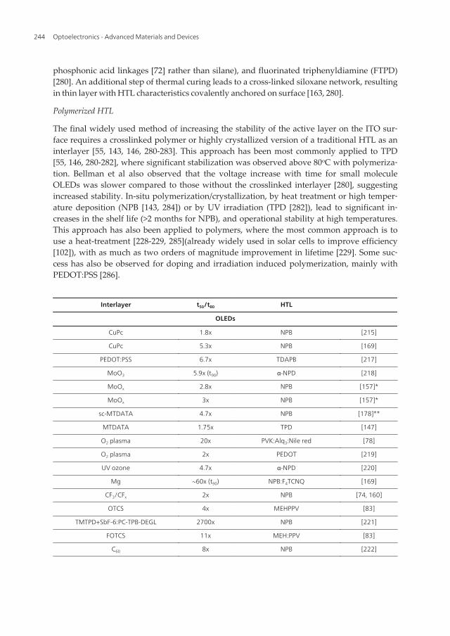
Interlayer t50/t80 HTL
OLEDs
CuPc 1.8x NPB [215]
CuPc 5.3x NPB [169]
PEDOT:PSS 6.7x TDAPB [217]
MoO3 5.9x (t90) α-NPD [218]
MoOx 2.8x NPB [157]*
MoOx 3x NPB [157]*
sc-MTDATA 4.7x NPB [178]**
MTDATA 1.75x TPD [147]
O2 plasma 20x PVK:Alq3:Nile red [78]
O2 plasma 2x PEDOT [219]
UV ozone 4.7x α-NPD [220]
Mg ~60x (t90) NPB:F4TCNQ [169]
CF3/CFx 2x NPB [74, 160]
OTCS 4x MEHPPV [83]
TMTPD+SbF-6:PC-TPB-DEGL 2700x NPB [221]
FOTCS 11x MEH:PPV [83]
C60 8x NPB [222]
Optoelectronics - Advanced Materials and Devices244

NTCDI-OCF3 1.2x NPB [159]
Pr2O3 ~7x CuPc/TPD [158]
Alq3 4.2x (t80) NPB [223]
ta-C orders of mag PEDOT [171]
Pani ~10x (t30) MEH:PPV [172]
NaCl:NPB 2.3x NPB [215]
metal free Pc:CuPc 3.4x TPTE [206]*
BHJ NPB:Alq 5.4x NPB [224]*
gradient HJ NPB:Alq 3.15x NPB [224]*
DSA_Ph:NPB 1.3x NPB [225]
F4TCNQ (5%-20%):NPB 40x NPB [169]
F4TCNQ (30%):NPB 14x NPB [169]
F4TCNQ (2%):NPB 2.5x NPB [169]
MADN:NPB 2.7x NPB [226]
PFI (3%):PEDOT:PSS 9.4x PFO [227]***
PFI (6%):PEDOT:PSS 8x PFO [227]***
heat treatment 35oc 3.5x MEH-PPV LB [228]
heat treatment 65oc 5.5x MEH-PPV LB [228]
heat treatment 110c 9.4x polyfluorene [229]***
heat treatment 150c 167.5x polyfluorene [229]***
OPVs
ZnPc ~3.5x ZnPc:C60 [63]
MoO3 ~ 4x H2TPP [75]
MoO3 ~24x α-NPD [75]
MoO3 ~27x P3HT:PCBM [230]***
MoOx ~80x PCDTBT:PC70BM [231]***
sMoOx 39x P3HT:PCBM [232]***
PEDOT 8.7x (t70) FFTCNQ/ZnPc:C60 [233]
* modified using data from [215] ** modified using data from [147] *** modified using data from [217]
1The most common description of lifetime for OLEDs is the illumination half-life (t50) – the time it takes for the lumi‐nance to decrease to half of its initial value [216]. In OPVs, a similar standard has been used with t50 defined as thetime for the power conversion efficiency (PCE) to decrease to half of its initial value [21]. More recently, it has becomemore common to report the t80, the time when the device has decayed to 80% of its initial performance [17]. In thischapter, t50 and t80 will be the commonly adopted lifetime values for OLEDs and OPVs respectively, unless otherwisestated.
Table 1. Relative improvement in t50 (for OLEDs) & t80 (for OPVs) compared to bare ITO for various interlayers used atthe ITO surface1
Dewetting Stability of ITO Surfaces in Organic Optoelectronic Deviceshttp://dx.doi.org/10.5772/52417
245
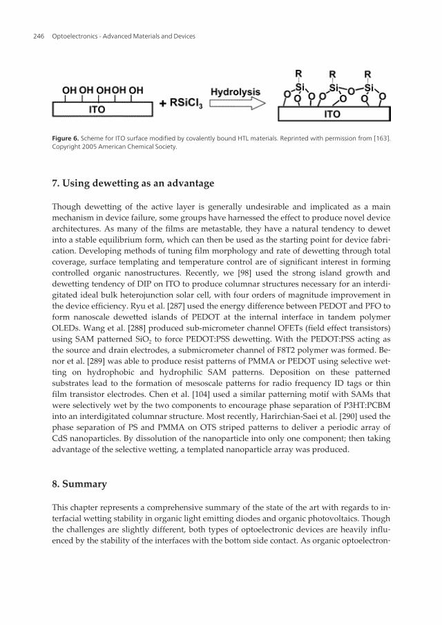
Figure 6. Scheme for ITO surface modified by covalently bound HTL materials. Reprinted with permission from [163].Copyright 2005 American Chemical Society.
7. Using dewetting as an advantage
Though dewetting of the active layer is generally undesirable and implicated as a mainmechanism in device failure, some groups have harnessed the effect to produce novel devicearchitectures. As many of the films are metastable, they have a natural tendency to dewetinto a stable equilibrium form, which can then be used as the starting point for device fabri‐cation. Developing methods of tuning film morphology and rate of dewetting through totalcoverage, surface templating and temperature control are of significant interest in formingcontrolled organic nanostructures. Recently, we [98] used the strong island growth anddewetting tendency of DIP on ITO to produce columnar structures necessary for an interdi‐gitated ideal bulk heterojunction solar cell, with four orders of magnitude improvement inthe device efficiency. Ryu et al. [287] used the energy difference between PEDOT and PFO toform nanoscale dewetted islands of PEDOT at the internal interface in tandem polymerOLEDs. Wang et al. [288] produced sub-micrometer channel OFETs (field effect transistors)using SAM patterned SiO2 to force PEDOT:PSS dewetting. With the PEDOT:PSS acting asthe source and drain electrodes, a submicrometer channel of F8T2 polymer was formed. Be‐nor et al. [289] was able to produce resist patterns of PMMA or PEDOT using selective wet‐ting on hydrophobic and hydrophilic SAM patterns. Deposition on these patternedsubstrates lead to the formation of mesoscale patterns for radio frequency ID tags or thinfilm transistor electrodes. Chen et al. [104] used a similar patterning motif with SAMs thatwere selectively wet by the two components to encourage phase separation of P3HT:PCBMinto an interdigitated columnar structure. Most recently, Harirchian-Saei et al. [290] used thephase separation of PS and PMMA on OTS striped patterns to deliver a periodic array ofCdS nanoparticles. By dissolution of the nanoparticle into only one component; then takingadvantage of the selective wetting, a templated nanoparticle array was produced.
8. Summary
This chapter represents a comprehensive summary of the state of the art with regards to in‐terfacial wetting stability in organic light emitting diodes and organic photovoltaics. Thoughthe challenges are slightly different, both types of optoelectronic devices are heavily influ‐enced by the stability of the interfaces with the bottom side contact. As organic optoelectron‐
Optoelectronics - Advanced Materials and Devices246
ic technologies mature, the metastability of interfaces becomes more and more significant inthe quest for greater performance.
Acknowledgements
The author would like to acknowledge collaborators at the Max-Planck-Institute for MetalsResearch, specifically Prof. Dr. H. Dosch and students supervised by the author (F. Maye, J.Heidkamp) who have contributed some experimental results to this chapter.
Author details
Ayse Turak
Department of Engineering Physics, McMaster University, Hamilton, Canada
References
[1] Krebs F C and Norrman K Analysis of the failure mechanism for a stable organicphotovoltaic during 10000 h of testing Prog Photovoltaics 2007;15(8) 697-712.
[2] Brabec C J, Hauch J A, Schilinsky P and Waldauf C Production Aspects of OrganicPhotovoltaics and Commercialization of Devices MRS Bulletin 2005;30(Jan) 50-2.
[3] Do L-m, Kim K, Zyung T and Kim J-j In situ investigation of degradation in polymer‐ic electroluminescent devices using time-resolved confocal laser scanning microscopeAppl Phys Lett 1997;70(25) 3470-2.
[4] Reese M O, Morfa A J, White M S, Kopidakis N, Shaheen S E, Rumbles G and GinleyD S Pathways for the degradation of organic photovoltaic P3HT: PCBM based devi‐ces Sol Energ Mat Sol C 2008;92(7) 746-52.
[5] Paci B, Generosi A, Albertini V R, Perfetti P, Bettignies R D and Sentein C Time-re‐solved morphological study of organic thin film solar cells based on calcium / alumi‐nium cathode material Chem Phys Lett 2008;461(1-3) 77-81.
[6] Jeranko T, Tributsch H, Sariciftci N S and Hummelen J C Patterns of efficiency anddegradation of composite polymer solar cells Sol Energ Mat Sol C 2004;83(2-3)247-62.
[7] Kuwabara T, Nakayama T, Uozumi K, Yamaguchi T and Takahashi K Highly dura‐ble inverted-type organic solar cell using amorphous titanium oxide as electron col‐lection electrode inserted between ITO and organic layer Sol Energ Mat Sol C2008;92(11) 1476-82.
Dewetting Stability of ITO Surfaces in Organic Optoelectronic Deviceshttp://dx.doi.org/10.5772/52417
247

[8] Cumpston B H, Parker I D and Jensen K F In situ characterization of the oxidativedegradation of a polymeric light emitting device J Appl Phys 2001;81(8) 3716-20.
[9] Scott J C, Kaufman J H, Brock P J, DiPietro R, Salem J and Goitia J A Degradation andfailure of MEH-PPV light-emitting diodes J Appl Phys 1996;79(5) 2745-51.
[10] Morgado J, Friend R H and Cacialli F Environmental aging of poly(p-phenyleneviny‐lene) based light-emitting diodes Synthetic Met 2000;114(2) 189-96.
[11] Dam N, Scurlock R D, Wang B J, Ma L C, Sundahl M and Ogilby P R Singlet oxygenas a reactive intermediate in the photodegradation of phenylenevinylene oligomersChem Mater 1999;11(5) 1302-5.
[12] Tang C W and Vanslyke S A Organic Electroluminescent Diodes Appl Phys Lett1987;51(12) 913-5.
[13] Tang C W 2-Layer Organic Photovoltaic Cell Appl Phys Lett 1986;48(2) 183-5.
[14] Opera project http://opera-project.eu/index.php?id=18&lang=EN; International Sum‐mit on Organic Photovoltaic Stability (ISOS) http://isos.wikispaces.com/; OLED100project http://OLED100.eu
[15] Kroon J M, Wienk M M and Hummelen J C Accurate efficiency determination andstability studies of conjugated polymeryfullerene solar cells Thin Solid Films2002;403-404(1 Feb) 223-8.
[16] Shrotriya V, Li G, Yao Y, Moriarty T, Emery K and Yang Y Accurate measurementand characterization of organic solar cells Adv Funct Mater 2006;16(15) 2016-23.
[17] Reese M O, Gevorgyan S A, Jorgensen M, Bundgaard E, Kurtz S R, Ginley D S, OlsonD C, Lloyd M T, Moryillo P, Katz E A, Elschner A, Haillant O, Currier T R, ShrotriyaV, Hermenau M, Riede M, Kirov K R, Trimmel G, Rath T, Inganas O, Zhang F L, An‐dersson M, Tvingstedt K, Lira-Cantu M, Laird D, McGuiness C, Gowrisanker S, Pan‐none M, Xiao M, Hauch J, Steim R, DeLongchamp D M, Rosch R, Hoppe H, EspinosaN, Urbina A, Yaman-Uzunoglu G, Bonekamp J B, van Breemen A J J M, Girotto C,Voroshazi E and Krebs F C Consensus stability testing protocols for organic photo‐voltaic materials and devices Sol Energ Mat Sol C 2011;95(5) 1253-67.
[18] Fery C, Racine B, Vaufrey D, Doyeux H and Cina S Physical mechanism responsiblefor the stretched exponential decay behavior of aging organic light-emitting diodesAppl Phys Lett 2005;87(21) 213502.
[19] De Bettignies R, Leroy J, Firon M and Sentein C Accelerated lifetime measurementsof P3HT: PCBM solar cells Synthetic Met 2006;156(7-8) 510-3.
[20] Schuller S, Schilinsky P, Hauch J and Brabec C J Determination of the degradationconstant of bulk heterojunction solar cells by accelerated lifetime measurementsAppl Phys a-Mater 2004;79(1) 37-40.
[21] Jorgensen M, Norrman K and Krebs F C Stability/degradation of polymer solar cellsSol Energ Mat Sol C 2008;92(7) 686-714.
Optoelectronics - Advanced Materials and Devices248
[22] Jørgensen M, Norrman K, Gevorgyan S A, Tromholt T, Andreasen B and Krebs F CStability of Polymer Solar Cells Adv Mater 2012;24(5) 580-612.
[23] So F and Kondakov D Degradation Mechanisms in Small-Molecule and Polymer Or‐ganic Light-Emitting Diodes Adv Mater 2010;22(34) 3762-77.
[24] A. Turak, Interfacial degradation in organic optoelectronics, RSC Adv., DOI:10.1039/C2RA22770C.
[25] Zinkeallmang M, Feldman L C and Grabow M H Clustering on Surfaces Surf Sci Rep1992;16(8) 377-463.
[26] Israelachvili J N Intermolecular and surface forces. Burlington, MA: Academic Press;2011.
[27] Strange T G, Evans D F and Hendrickson W A Nucleation and Growth of DefectsLeading to Dewetting of Thin Polymer Films Langmuir 1997;13(16) 4459-65.
[28] Kheshgi H S and Scriven L E Dewetting - Nucleation and Growth of Dry RegionsChem Eng Sci 1991;46(2) 519-26.
[29] Hamaker H C The London – van der Waals attraction between spherical particlesPhysica 1937; 4(10) 1058-72.
[30] Chattopadhyay S and Meredith J C Combinatorial screening of organic electronicmaterials: thin film stability Measurement Science and Technology 2005;16(1) 128-36.
[31] Xie R, Karim A, Douglas J F, Han C C and Weiss R A Spinodal Dewetting of ThinPolymer Films Phys Rev Lett 1998;81(6) 1251-4.
[32] Barnes K A, Karim A, Douglas J F, Nakatani A I, Gruell H and Amis E J Suppressionof Dewetting in Nanoparticle-Filled Polymer Films Macromolecules 2000;33(11)4177-85.
[33] Mukherjee R, Das S, Das A, Sharma S K, Raychaudhuri A K and Sharma A Stabilityand Dewetting of Metal Nanoparticle Filled Thin Polymer Films: Dynamics ACSNano 2010;4(7) 3709-24.
[34] Reiter G Mobility of Polymers in Films Thinner Than Their Unperturbed Size Euro‐phys Lett 1993;23(8) 579-84.
[35] Jacobs K, Herminghaus S and Mecke K R Thin liquid polymer films rupture via de‐fects Langmuir 1998;14(4) 965-9.
[36] Reiter G, Hamieh M, Damman P, Sclavons S, Gabriele S, Vilmin T and Raphael E Re‐sidual stresses in thin polymer films cause rupture and dominate early stages ofdewetting Nat Mater 2005;4(10) 754-8.
[37] Sharma A, Mittal J and Verma R Instability and dewetting of thin films induced bydensity variations Langmuir 2002;18(26) 10213-20.
Dewetting Stability of ITO Surfaces in Organic Optoelectronic Deviceshttp://dx.doi.org/10.5772/52417
249
[38] Fenter P, Schreiber F, Bulovic V and Forrest S R Thermally induced failure mecha‐nisms of organic light emitting device structures probed by X-ray specular reflectivi‐ty Chem Phys Lett 1997;277(5-6) 521-6.
[39] Vansmaalen S, Deboer J L, Haas C and Kommandeur J Anisotropic Thermal-Expan‐sion in Crystals with Stacks of Planar Molecules, Such as Tetracyanoquinodimetha‐nide (Tcnq) Salts Phys Rev B 1985;31(6) 3496-503.
[40] Vix A B E, Mu P, Stocker W, Stamm M and Rabe J P Crossover between Dewettingand Stabilization of Ultrathin Liquid Crystalline Polymer Films Langmuir2000;16(26) 10456-62.
[41] Krause B, Durr A C, Schreiber F, Dosch H and Seeck O H Thermal stability and parti‐al dewetting of crystalline organic thin films: 3,4,9,10-perylenetetracarboxylic dia‐nhydride on Ag(111) J Chem Phys 2003;119(6) 3429-35.
[42] Burke S A, Topple J M and Guttter P Molecular dewetting on insulators Journal ofPhysics: Condensed Matter 2009;21(42) 423101.
[43] Adachi C, Tsutsui T and Saito S Blue Light-Emitting Organic Electroluminescent De‐vices Appl Phys Lett 1990;56(9) 799-801.
[44] Appleyard S F J, Day S R, Pickford R D and Willis M R Organic electroluminescentdevices: enhanced carrier injection using SAM derivatized ITO electrodes J MaterChem 2000;10(1) 169-73.
[45] Malinsky J E, Jabbour G E, Shaheen S E, Anderson J D, Richter A G, Marks T J, Arm‐strong N R, Kippelen B, Dutta P and Peyghambarian N Self-assembly processes fororganic LED electrode passivation and charge injection balance Adv Mater 1999;11(3)227-31.
[46] Shen Y L, Jacobs D B, Malliaras G G, Koley G, Spencer M G and Ioannidis A Modifi‐cation of indium tin oxide for improved hole injection in organic light emitting di‐odes Adv Mater 2001;13(16) 1234-8.
[47] Nuesch F, Forsythe E W, Le Q T, Gao Y and Rothberg L J Importance of indium tinoxide surface acido basicity for charge injection into organic materials based lightemitting diodes J Appl Phys 2000;87(11) 7973-80.
[48] Ke L, Chua S J, Zhang K R and Chen P Bubble formation due to electrical stress inorganic light emitting devices Appl Phys Lett 2002;80(2) 171-3.
[49] Liu G, Kerr J B and Johnson S Dark spot formation relative to ITO surface roughnessfor polyfluorene devices Synthetic Met 2004;144(1) 1-6.
[50] Scott J C, Carter S A, Karg S and Angelopoulos M Polymeric anodes for organiclight-emitting diodes Synthetic Met 1997;85(1-3) 1197-200.
[51] Adachi C, Nagai K and Tamoto N Molecular Design of Hole Transport Materials forObtaining High Durability in Organic Electroluminescent Diodes Appl Phys Lett1995;66(20) 2679-81.
Optoelectronics - Advanced Materials and Devices250
[52] Gong X, Moses D, Heeger A J, Liu S and Jen A K Y High-performance polymer light-emitting diodes fabricated with a polymer hole injection Appl Phys Lett 2003;83(1)183-5.
[53] Naito K and Miura A Molecular Design for Nonpolymeric Organic-Dye Glasses withThermal-Stability - Relations between Thermodynamic Parameters and AmorphousProperties J Phys Chem 1993;97(23) 6240-8.
[54] D'Iorio M Molecular materials for microelectronics Can J Phys 2000;78(3) 231-41.
[55] Shirota Y Organic materials for electronic and optoelectronic devices J Mater Chem2000;10(1) 1-25.
[56] Shirota Y and Kageyama H Charge carrier transporting molecular materials and theirapplications in devices Chem Rev 2007;107(4) 953-1010.
[57] Hung L S and Chen C H Recent progress of molecular organic electroluminescentmaterials and devices Mat Sci Eng R 2002;39(5-6) 143-222.
[58] Rothberg L J and Lovinger A J Status of and prospects for organic electrolumines‐cence J Mater Res 1996;11(12) 3174-87.
[59] Hains A W, Liang Z Q, Woodhouse M A and Gregg B A Molecular Semiconductorsin Organic Photovoltaic Cells Chem Rev 2010;110(11) 6689-735.
[60] Cao Y, Yu G, Zhang C, Menon R and Heeger A J Polymer light-emitting diodes withpolyethylene dioxythiophene-polystyrene sulfonate as the transparent anode Syn‐thetic Met 1997;87(2) 171-4.
[61] Ishii H, Sugiyama K, Ito E and Seki K Energy level alignment and interfacial elec‐tronic structures at organic metal and organic organic interfaces Adv Mater1999;11(8) 605-25.
[62] Kim H, Pique A, Horwitz J S, Mattoussi H, Murata H, Kafafi Z H and Chrisey D BIndium tin oxide thin films for organic light-emitting devices Appl Phys Lett1999;74(23) 3444-6.
[63] Schafer S, Petersen A, Wagner T A, Kniprath R, Lingenfelser D, Zen A, Kirchartz T,Zimmermann B, Wurfel U, Feng X J and Mayer T Influence of the indium tin oxide/organic interface on open-circuit voltage, recombination, and cell degradation in or‐ganic small-molecule solar cells Phys Rev B 2011;83(16) 165311.
[64] Tak Y H, Kim K B, Park H G, Lee K H and Lee J R Criteria for ITO (indium-tin-oxide)an organic light thin film as the bottom electrode of emitting diode Thin Solid Films2002;411(1) 12-6.
[65] Kim J S, Granstrom M, Friend R H, Johansson N, Salaneck W R, Daik R, Feast W Jand Cacialli F Indium-tin oxide treatments for single- and double-layer polymericlight-emitting diodes: The relation between the anode physical, chemical, and mor‐phological properties and the device performance J Appl Phys 1998;84(12) 6859-70.
Dewetting Stability of ITO Surfaces in Organic Optoelectronic Deviceshttp://dx.doi.org/10.5772/52417
251
[66] Djurisic A B, Lau T N, Kwong C Y, Guo W L, Bai Y K, Li E H and Chan W K Surfacetreatments of indium-tin-oxide substrates: comprehensive investigation of mechani‐cal, chemical, thermal, and plasma treatments Proc SPIE 2002;4464 273-80.
[67] Huang Z H, Zeng X T, Sun X Y, Kang E T, Fuh J Y H and Lu L Influence of plasmatreatment of ITO surface on the growth and properties of hole transport layer andthe device performance of OLEDs Org Electron 2008;9(1) 51-62.
[68] Goncalves-Conto S, Carrard M, Si-Ahmed L and Zuppiroli L Interface morphologyin organic light-emitting diodes Adv Mater 1999;11(2) 112-5.
[69] Shen Y L, Klein M W, Jacobs D B, Scott J C and Malliaras G G Mobility-dependentcharge injection into an organic semiconductor Phys Rev Lett 2001;86(17) 3867-70.
[70] Gonzalez G B, Cohen J B, Hwang J H, Mason T O, Hodges J P and Jorgensen J DNeutron diffraction study on the defect structure of indium-tin-oxide J Appl Phys2001;89(5) 2550-5.
[71] Kim H, Gilmore C M, Pique A, Horwitz J S, Mattoussi H, Murata H, Kafafi Z H andChrisey D B Electrical, optical, and structural properties of indium-tin-oxide thinfilms for organic light-emitting devices J Appl Phys 1999;86(11) 6451-61.
[72] Paramonov P B and Paniagua S A Theoretical Characterization of the Indium Tin Ox‐ide Surface and of Its Binding Sites for Adsorption of Phosphonic Acid MonolayersChem Mater 2008;20(16) 5131-3.
[73] Armstrong N R, Veneman P A, Ratcliff E, Placencia D and Brumbach M Oxide Con‐tacts in Organic Photovoltaics: Characterization and Control of Near-Surface Compo‐sition in Indium-Tin Oxide (ITO) Electrodes Accounts Chem Res 2009;42(11) 1748-57.
[74] Tang J X, Li Y Q, Zheng L R and Hung L S Anode/organic interface modification byplasma polymerized fluorocarbon films J Appl Phys 2004;95(8) 4397-403.
[75] Kanai Y, Matsushima T and Murata H Improvement of stability for organic solarcells by using molybdenum trioxide buffer layer Thin Solid Films 2009;518(2) 537-40.
[76] Milliron D J, Hill I G, Shen C, Kahn A and Schwartz J Surface oxidation activates in‐dium tin oxide for hole injection J Appl Phys 2000;87(1) 572-6.
[77] Sharma A, Kippelen B, Hotchkiss P J and Marder S R Stabilization of the work func‐tion of indium tin oxide using organic surface modifiers in organic light-emitting di‐odes Appl Phys Lett 2008;93(16)
[78] Wu C C, Wu C I, Sturm J C and Kahn A Surface modification of indium tin oxide byplasma treatment: An effective method to improve the efficiency, brightness, and re‐liability of organic light emitting devices Appl Phys Lett 1997;70(11) 1348-50.
[79] Koch N, Kahn A, Ghijsen J, Pireaux J J, Schwartz J, Johnson R L and Elschner A Con‐jugated organic molecules on metal versus polymer electrodes: Demonstration of akey energy level alignment mechanism Appl Phys Lett 2003;82(1) 70-2.
Optoelectronics - Advanced Materials and Devices252
[80] Cui J, Huang Q L, Veinot J C G, Yan H, Wang Q W, Hutchison G R, Richter A G,Evmenenko G, Dutta P and Marks T J Anode interfacial engineering approaches toenhancing anode/hole transport layer interfacial stability and charge injection effi‐ciency in organic light-emitting diodes Langmuir 2002;18(25) 9958-70.
[81] Lee J, Jung B-j, Lee J-i, Chu Y, Do L-m and Shim H-k Modification of an ITO anodewith a hole-transporting SAM for improved OLED device characteristics J MaterChem 2002;12 3494-8.
[82] Chong L-w, Lee Y-l and Wen T-c Surface modification of indium tin oxide anodes byself-assembly monolayers: Effects on interfacial morphology and charge injection inorganic light-emitting diodes Thin Solid Films 2007;515(5) 2833-41.
[83] Choi B, Rhee J and Lee H H Tailoring of self-assembled monolayer for polymer light-emitting diodes Appl Phys Lett 2001;79(13) 2109-11.
[84] Lacher S, Matsuo Y and Nakamura E Molecular and Supramolecular Control of theWork Function of an Inorganic Electrode with Self-Assembled Monolayer of Umbrel‐la-Shaped Fullerene Derivatives J Am Chem Soc 2011;133(42) 16997-7004.
[85] You Z Z Combined AFM, XPS, and contact angle studies on treated indium-tin-oxidefilms for organic light-emitting devices Mater Lett 2007;61(18) 3809-14.
[86] Poon C O, Wong F L, Tong S W, Zhang R Q, Lee C S and Lee S T Improved perform‐ance and stability of organic light-emitting devices with silicon oxy-nitride bufferlayer Appl Phys Lett 2003;83(5) 1038-40.
[87] Le Q T, Forsythe E W, Nuesch F, Rothberg L J, Yan L and Gao Y Interface formationbetween NPB and processed indium tin oxide Thin Solid Films 2000;363(1-2) 42-6.
[88] Grozea D, Turak A, Yuan Y, Han S, Lu Z H and Kim W Y Enhanced thermal stabilityin organic light-emitting diodes through nanocomposite buffer layers at the anode/organic interface J Appl Phys 2007;101(3) 033522.
[89] Ribic P R and Bratina G Initial stages of growth of organic semiconductors on vicinal(0 0 0 1) sapphire surfaces Surface Science 2008;602(7) 1368-75.
[90] Ettedgui E, Davis G T, Hu B and Karasz F E Degradation of polymer-based light-emitting diodes during operation Synthetic Met 1997;90(1) 73-6.
[91] Durr A C, Schreiber F, Munch M, Karl N, Krause B, Kruppa V and Dosch H Highstructural order in thin films of the organic semiconductor diindenoperylene ApplPhys Lett 2002;81(12) 2276-8.
[92] Durr A C, Schreiber F, Ritley K A, Kruppa V, Krug J, Dosch H and Struth B Rapidroughening in thin film growth of an organic semiconductor (diindenoperylene)Phys Rev Lett 2003;90(1) 016104.
[93] Zhang X N, Barrena E, de Oteyza D G and Dosch H Transition from layer-by-layer torapid roughening in the growth of DIP on SiO2 Surface Science 2007;601(12) 2420-5.
Dewetting Stability of ITO Surfaces in Organic Optoelectronic Deviceshttp://dx.doi.org/10.5772/52417
253
[94] Ramaniah L M and Boero M Structural, electronic, and optical properties of the diin‐denoperylene molecule from first-principles density-functional theory Phys Rev A2006;74(4) 042505.
[95] Karl N Charge carrier transport in organic semiconductors Synthetic Met2003;133-134(13 March) 649-57.
[96] Huang Y L, Chen W, Huang H, Qi D C, Chen S, Gao X Y, Pflaum J and Wee A T SUltrathin Films of Diindenoperylene on Graphite and SiO2 J Phys Chem C2009;113(21) 9251-5.
[97] Kurrle D and Pflaum J Exciton diffusion length in the organic semiconductor diinde‐noperylene Appl Phys Lett 2008;92(13) 133306.
[98] Turak A, Nguyen M, Maye F, Heidkamp J, Lienerth P, Wrachtrup J and Dosch HNanoscale Engineering of Exciton Dissociating Interfaces in Organic Photovoltaics JNano Res 2011;14 125-36.
[99] Heidkamp J. DIP growth on substrates relevant for organic solar cells.Diploma the‐sis.University of Stuttgart;2009.
[100] Zhu Z, Hadjikyriacou S, Waller D and Gaudiana R Stabilization of film morphologyin polymer-fullerene heterojunction solar cells J Macromol Sci Pure 2004;A41(12)1467-87.
[101] Bertho S, Haeldermans I, Swinnen A, Moons W, Martens T, Lutsen L, VanderzandeD, Manca J, Senes A and Bonfiglio A Influence of thermal ageing on the stability ofpolymer bulk heterojunction solar cells Sol Energ Mat Sol C 2007;91(5) 385-9.
[102] Turak A, Hanisch J, Barrena E, Welzel U, Widmaier F, Ahlswede E and Dosch H Sys‐tematic analysis of processing parameters on the ordering and performance of work‐ing poly(3-hexyl-thiophene):[6,6]-phenyl C(61)-butyric acid methyl ester solar cells JRenew Sustain Ener 2010;2(5) 053103.
[103] Bulliard X, Ihn S G, Yun S, Kim Y, Choi D, Choi J Y, Kim M, Sim M, Park J H, Choi Wand Cho K Enhanced Performance in Polymer Solar Cells by Surface Energy ControlAdv Funct Mater 2010;20(24) 4381-7.
[104] Chen F C, Lin Y K and Ko C J Submicron-scale manipulation of phase separation inorganic solar cells Appl Phys Lett 2008;92(2) 023307.
[105] Bjorstrom C M, Nilsson S, Bernasik A, Budkowski A, Andersson M, Magnusson K Oand Moons E Vertical phase separation in spin-coated films of a low bandgap poly‐fluorene/PCBM blend - Effects of specific substrate interaction Appl Surf Sci2007;253(8) 3906-12.
[106] Gardonio S, Gregoratti L, Melpignano P, Aballe L, Biondo V, Zamboni R, Murgia M,Caria S and Kiskinova A Degradation of organic light-emitting diodes under differ‐ent environment at high drive conditions Org Electron 2007;8(1) 37-43.
Optoelectronics - Advanced Materials and Devices254
[107] Luo Y, Aziz H, Popovic Z D and Xu G Correlation between electroluminescence effi‐ciency and stability in organic light-emitting devices under pulsed driving condi‐tions J Appl Phys 2006;99(5) 054508.
[108] Gärditz C and Winnacker A Impact of Joule heating on the brightness homogeneityof organic light Appl Phys Lett 2007;90(10) 103506.
[109] Chao C I, Chuang K R and Chen S A Failure phenomena and mechanisms of poly‐meric light-emitting diodes: Indium-tin-oxide-damage Appl Phys Lett 1996;69(19)2894-6.
[110] Zhou X, He J, Liao L S, Lu M, Ding X M, Hou X Y, Zhang X M, He X Q and Lee S TReal-time observation of temperature rise and thermal breakdown processes in or‐ganic LEDs using an IR imaging and analysis system Adv Mater 2000;12(4) 265-9.
[111] Tessler N, Harrison N T, Thomas D S and Friend R H Current heating in polymerlight emitting diodes Appl Phys Lett 1998;73(6) 732-4.
[112] Nakanotani H, Sasabe H and Adachi C Singlet-singlet and singlet-heat annihilationsin fluorescence-based organic light-emitting diodes under steady-state high currentdensity Appl Phys Lett 2005;86(21) 213506.
[113] Zhan Y Q, Xiong Z H, Shi H Z, Zhang S T, Xu Z, Zhong G Y, He J, Zhao J M, Wang ZJ, Obbard E, Ding H J, Wang X J, Ding X M, Huang W and Hou X Y Sodium stearate ,an effective amphiphilic molecule buffer material between organic and metal layersin organic light-emitting devices Appl Phys Lett 2003;83(8) 1656-8.
[114] Choi S H, Lee T I, Baik H K, Roh H H, Kwon O and Suh D H The effect of electrodeheat sink in organic-electronic devices Appl Phys Lett 2008;93(18) 183301.
[115] Sullivan P and Jones T S Pentacene / fullerene ( C 60 ) heterojunction solar cells: De‐vice performance and degradation mechanisms Org Electron 2008;9(5) 656-60.
[116] Paci B, Generosi A, Albertini V R, Generosi R, Perfetti P, de Bettignies R and SenteinC Time-resolved morphological study of bulk heterojunction films for efficient or‐ganic solar devices J Phys Chem C 2008;112(26) 9931-6.
[117] Franke R, Maennig B, Petrich A and Pfeiffer M Long-term stability of tandem solarcells containing small organic molecules Sol Energ Mat Sol C 2008;92(7) 732-5.
[118] Xu M S, Xu J B and An J Visualization of thermally activated morphology evolutionof N,N'-di(naphthalene-1-yl)-N,N'-diphthalbenzidine films on ITO/copper phthalo‐cyanine underlying layer Appl Phys a-Mater 2005;81(6) 1151-6.
[119] Han E M, Do L M, Yamamoto N and Fujihira M Study of Interfacial Degradation ofthe Vapor-Deposited Bilayer of Alq3/Tpd for Organic Electroluminescent (El) Devi‐ces by Photoluminescence Chem Lett 1995;24(1) 57-8.
[120] Tokito S and Taga Y Organic Electroluminescent Devices Fabricated Using a Dia‐mine Doped Mgf2 Thin-Film as a Hole-Transporting Layer Appl Phys Lett 1995;66(6)673-5.
Dewetting Stability of ITO Surfaces in Organic Optoelectronic Deviceshttp://dx.doi.org/10.5772/52417
255
[121] Loy B D E, Koene B E and Thompson M E Thermally Stable Hole-Transporting Mate‐rials Based upon a Fluorene Core Adv Funct Mater 2002;12(4) 245-9.
[122] Orita K, Morimura T, Horiuchi T and Matsushige K In situ energy-dispersive X-rayreflectivity measurements of structural changes in thin films for organic electrolumi‐nescent devices Synthetic Met 1997;91(1-3) 155-8.
[123] Tokito S, Tanaka H, Noda K, Okada A and Taga Y Thermal stability in oligomerictriphenylamine / tris ( 8-quinolinolato ) aluminum electroluminescent devices ApplPhys Lett 1997;70(15) 1929-31.
[124] Brown T M, Kim J S, Friend R H, Cacialli F, Daik R and Feast W J Built-in field elec‐troabsorption spectroscopy of polymer light-emitting diodes incorporating a dopedpoly(3,4-ethylene dioxythiophene) hole injection layer Appl Phys Lett 1999;75(12)1679-81.
[125] Xu M S and Xu J B Real-time visualization of thermally activated degradation of theITO/CuPC/NPB/Alq(3) stack used in one of the organic light-emitting diodes J PhysD Appl Phys 2004;37(12) 1603-8.
[126] Hoppe H, Niggemann M, Winder C, Kraut J, Hiesgen R, Hinsch A, Meissner D andSariciftci N S Nanoscale morphology of conjugated polymer/fullerene-based bulk-heterojunction solar cells Adv Funct Mater 2004;14(10) 1005-11.
[127] Yang X N, van Duren J K J, Janssen R A J, Michels M A J and Loos J Morphology andthermal stability of the active layer in poly(p-phenylenevinylene)/methanofullereneplastic photovoltaic devices Macromolecules 2004;37(6) 2151-8.
[128] Motaung D E, Malgas G F and Arendse C J Insights into the stability and thermaldegradation of P3HT:C-60 blended films for solar cell applications J Mater Sci2011;46(14) 4942-52.
[129] Conings B, Bertho S, Vandewal K, Senes A, Haen J D, Conings B, Bertho S, VandewalK, Senes A, Haen J D, Manca J and Janssen R A J Modeling the temperature induceddegradation kinetics of the short circuit current in organic bulk heterojunction solarcells Appl Phys Lett 2010;96(16) 163301.
[130] Bertho S, Janssen G, Cleij T J, Conings B, Moons W, Gadisa A, Haen J D, Goovaerts E,Lutsen L, Manca J and Vanderzande D Effect of temperature on the morphologicaland photovoltaic stability of bulk heterojunction polymer: fullerene solar cells SolEnerg Mat Sol C 2008;92(7) 753-60.
[131] Luo Y C, Aziz H, Xu G and Popovic Z D Improving the stability of organic light-emitting devices by using a hole-injection-tunable-anode-buffer-layer J Appl Phys2007;101(5) 054512.
[132] Forsythe E W, Abkowitz M A and Gao Y L Tuning the carrier injection efficiency fororganic light-emitting diodes J Phys Chem B 2000;104(16) 3948-52.
Optoelectronics - Advanced Materials and Devices256
[133] van Slyke S A, Chen C H and Tang C W Organic electroluminescent devices with im‐proved stability Appl Phys Lett 1996;69(15) 2160-2.
[134] Lee Y-j, Lee H, Byun Y, Song S, Kim J-e, Eom D, Cha W, Park S-s, Kim J and Kim HStudy of thermal degradation of organic light emitting device structures by X-rayscattering Thin Solid Films 2007;515(14) 5674-7.
[135] Sellner B S, Gerlach A, Schreiber F, Kelsch M, Kasper N, Dosch H, Meyer S, Pflaum J,Fischer M and Gompf B Strongly Enhanced Thermal Stability of Crystalline OrganicThin Films Induced by Aluminum Oxide Capping Layers Adv Mater 2004;16(19)1750-3.
[136] Peumans P, Uchida S and Forrest S R Efficient bulk heterojunction photovoltaic cellsusing small- molecular-weight organic thin films Nature 2003;425(September) 158-62.
[137] Durr A C, Koch N, Kelsch M, Ruhm A, Ghijsen J, Johnson R L, Pireaux J J, Schwartz J,Schreiber F, Dosch H and Kahn A Interplay between morphology, structure, andelectronic properties at diindenoperylene-gold interfaces Phys Rev B 2003;68(11)115428.
[138] Zhang F, Baralia G, Boborodea A, Bailly C, Nysten B and Jonas A M Partial Dewet‐ting of Polyethylene Thin Films on Rough Silicon Dioxide Surfaces Langmuir2005;21(16) 7427-32.
[139] Karapanagiotis I, Evans D F and Gerberich W W Dewetting dynamics of thin poly‐styrene films from sputtered silicon and gold surfaces Colloid Surface A2002;207(1-3) 59-67.
[140] Netz R R and Andelman D Roughness-induced wetting Physical Review E 1997;55(1)687-700.
[141] Wirth H O Organische Gläser mit hohen Glasumwandlungstemperaturen auf Basisniedermolekularer Verbindungen Die Angewandte Makromolekulare Chemie1991;185(1) 329-34.
[142] O'Brien D F, Burrows P E, Forrest S R, Koene B E, Loy D E and Thompson M E HoleTransporting Materials with High Glass Transition Temperatures for Use in OrganicLight-Emitting Devices Adv Mater 1998;10(14) 1108-12.
[143] Gao Z Q, Lai W Y, Wong T C, Lee C S and Bello I Organic electroluminescent devicesby high-temperature processing and crystalline hole transporting layer Appl PhysLett 1999;74(22) 3269-71.
[144] Xu M S, Xu J B, Chen H Z and Wang M Nanoscale investigation of moisture-induceddegradation mechanisms of tris ( 8-hydroxyquinoline ) aluminium-based organiclight-emitting Journal of Physics D: Applied Physics 2004;37(18) 2618-22.
[145] Sato Y, Ogata T, Ichinosawa S, Fugono M and Kanai H Interface and material consid‐erations of OLEDs Proc SPIE 1999;3797 198-208.
Dewetting Stability of ITO Surfaces in Organic Optoelectronic Deviceshttp://dx.doi.org/10.5772/52417
257
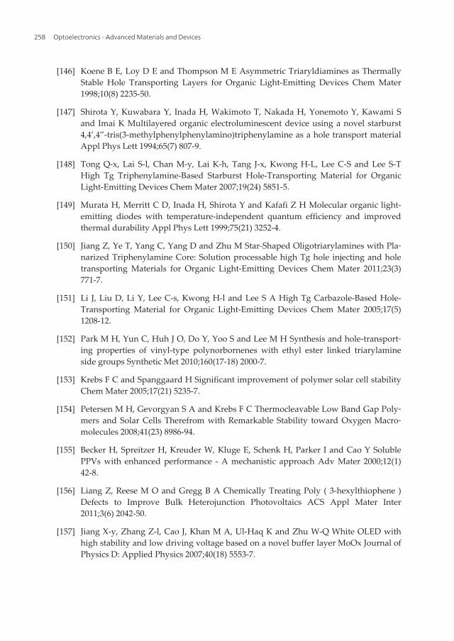
[146] Koene B E, Loy D E and Thompson M E Asymmetric Triaryldiamines as ThermallyStable Hole Transporting Layers for Organic Light-Emitting Devices Chem Mater1998;10(8) 2235-50.
[147] Shirota Y, Kuwabara Y, Inada H, Wakimoto T, Nakada H, Yonemoto Y, Kawami Sand Imai K Multilayered organic electroluminescent device using a novel starburst4,4’,4”-tris(3-methylphenylphenylamino)triphenylamine as a hole transport materialAppl Phys Lett 1994;65(7) 807-9.
[148] Tong Q-x, Lai S-l, Chan M-y, Lai K-h, Tang J-x, Kwong H-L, Lee C-S and Lee S-THigh Tg Triphenylamine-Based Starburst Hole-Transporting Material for OrganicLight-Emitting Devices Chem Mater 2007;19(24) 5851-5.
[149] Murata H, Merritt C D, Inada H, Shirota Y and Kafafi Z H Molecular organic light-emitting diodes with temperature-independent quantum efficiency and improvedthermal durability Appl Phys Lett 1999;75(21) 3252-4.
[150] Jiang Z, Ye T, Yang C, Yang D and Zhu M Star-Shaped Oligotriarylamines with Pla‐narized Triphenylamine Core: Solution processable high Tg hole injecting and holetransporting Materials for Organic Light-Emitting Devices Chem Mater 2011;23(3)771-7.
[151] Li J, Liu D, Li Y, Lee C-s, Kwong H-l and Lee S A High Tg Carbazole-Based Hole-Transporting Material for Organic Light-Emitting Devices Chem Mater 2005;17(5)1208-12.
[152] Park M H, Yun C, Huh J O, Do Y, Yoo S and Lee M H Synthesis and hole-transport‐ing properties of vinyl-type polynorbornenes with ethyl ester linked triarylamineside groups Synthetic Met 2010;160(17-18) 2000-7.
[153] Krebs F C and Spanggaard H Significant improvement of polymer solar cell stabilityChem Mater 2005;17(21) 5235-7.
[154] Petersen M H, Gevorgyan S A and Krebs F C Thermocleavable Low Band Gap Poly‐mers and Solar Cells Therefrom with Remarkable Stability toward Oxygen Macro‐molecules 2008;41(23) 8986-94.
[155] Becker H, Spreitzer H, Kreuder W, Kluge E, Schenk H, Parker I and Cao Y SolublePPVs with enhanced performance - A mechanistic approach Adv Mater 2000;12(1)42-8.
[156] Liang Z, Reese M O and Gregg B A Chemically Treating Poly ( 3-hexylthiophene )Defects to Improve Bulk Heterojunction Photovoltaics ACS Appl Mater Inter2011;3(6) 2042-50.
[157] Jiang X-y, Zhang Z-l, Cao J, Khan M A, Ul-Haq K and Zhu W-Q White OLED withhigh stability and low driving voltage based on a novel buffer layer MoOx Journal ofPhysics D: Applied Physics 2007;40(18) 5553-7.
Optoelectronics - Advanced Materials and Devices258
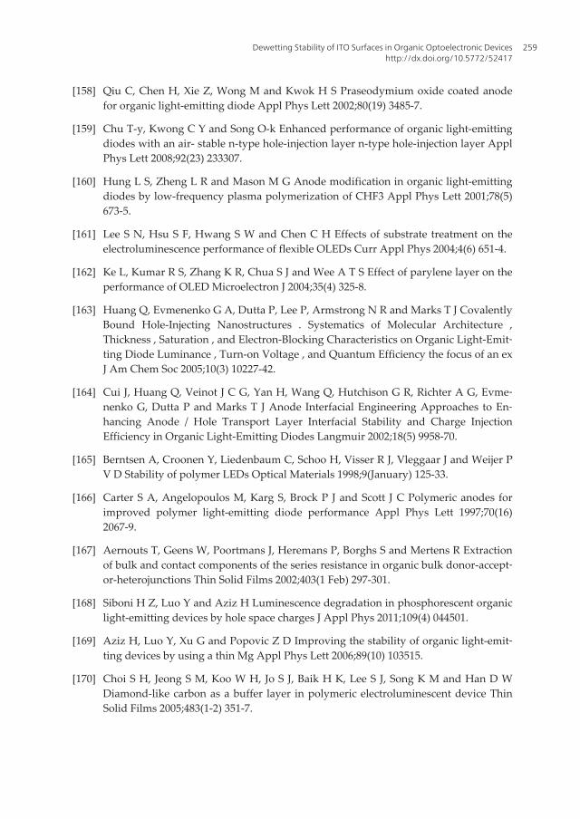
[158] Qiu C, Chen H, Xie Z, Wong M and Kwok H S Praseodymium oxide coated anodefor organic light-emitting diode Appl Phys Lett 2002;80(19) 3485-7.
[159] Chu T-y, Kwong C Y and Song O-k Enhanced performance of organic light-emittingdiodes with an air- stable n-type hole-injection layer n-type hole-injection layer ApplPhys Lett 2008;92(23) 233307.
[160] Hung L S, Zheng L R and Mason M G Anode modification in organic light-emittingdiodes by low-frequency plasma polymerization of CHF3 Appl Phys Lett 2001;78(5)673-5.
[161] Lee S N, Hsu S F, Hwang S W and Chen C H Effects of substrate treatment on theelectroluminescence performance of flexible OLEDs Curr Appl Phys 2004;4(6) 651-4.
[162] Ke L, Kumar R S, Zhang K R, Chua S J and Wee A T S Effect of parylene layer on theperformance of OLED Microelectron J 2004;35(4) 325-8.
[163] Huang Q, Evmenenko G A, Dutta P, Lee P, Armstrong N R and Marks T J CovalentlyBound Hole-Injecting Nanostructures . Systematics of Molecular Architecture ,Thickness , Saturation , and Electron-Blocking Characteristics on Organic Light-Emit‐ting Diode Luminance , Turn-on Voltage , and Quantum Efficiency the focus of an exJ Am Chem Soc 2005;10(3) 10227-42.
[164] Cui J, Huang Q, Veinot J C G, Yan H, Wang Q, Hutchison G R, Richter A G, Evme‐nenko G, Dutta P and Marks T J Anode Interfacial Engineering Approaches to En‐hancing Anode / Hole Transport Layer Interfacial Stability and Charge InjectionEfficiency in Organic Light-Emitting Diodes Langmuir 2002;18(5) 9958-70.
[165] Berntsen A, Croonen Y, Liedenbaum C, Schoo H, Visser R J, Vleggaar J and Weijer PV D Stability of polymer LEDs Optical Materials 1998;9(January) 125-33.
[166] Carter S A, Angelopoulos M, Karg S, Brock P J and Scott J C Polymeric anodes forimproved polymer light-emitting diode performance Appl Phys Lett 1997;70(16)2067-9.
[167] Aernouts T, Geens W, Poortmans J, Heremans P, Borghs S and Mertens R Extractionof bulk and contact components of the series resistance in organic bulk donor-accept‐or-heterojunctions Thin Solid Films 2002;403(1 Feb) 297-301.
[168] Siboni H Z, Luo Y and Aziz H Luminescence degradation in phosphorescent organiclight-emitting devices by hole space charges J Appl Phys 2011;109(4) 044501.
[169] Aziz H, Luo Y, Xu G and Popovic Z D Improving the stability of organic light-emit‐ting devices by using a thin Mg Appl Phys Lett 2006;89(10) 103515.
[170] Choi S H, Jeong S M, Koo W H, Jo S J, Baik H K, Lee S J, Song K M and Han D WDiamond-like carbon as a buffer layer in polymeric electroluminescent device ThinSolid Films 2005;483(1-2) 351-7.
Dewetting Stability of ITO Surfaces in Organic Optoelectronic Deviceshttp://dx.doi.org/10.5772/52417
259

[171] Chen B J, Sun X W and Tay B K Improvement of efficiency and stability of polymerlight-emitting devices by modifying indium tin oxide anode surface with ultrathintetrahedral amorphous carbon film Appl Phys Lett 2005;86(6) 063506.
[172] Karg S, Scott J C, Salem J R and Angelopoulos M Increased brightness and lifetime ofpolymer light-emitting diodes with polyaniline anodes Synthetic Met 1996;80(2)111-7.
[173] Wong K W, Yip H L, Luo Y, Wong K Y, Lau W M, Low K H, Chow H F, Gao Z Q,Yeung W L and Chang C C Blocking reactions between indium-tin oxide and poly(3,4-ethylene dioxythiophene): poly(styrene sulphonate) with a self-assembly mono‐layer Appl Phys Lett 2002;80(15) 2788-90.
[174] de Jong M P, van IJzendoorn L J and de Voigt M J A Stability of the interface betweenindium-tin-oxide and poly(3,4-ethylenedioxythiophene)/poly(styrenesulfonate) inpolymer light-emitting diodes Appl Phys Lett 2000;77(14) 2255-7.
[175] Chua S J, Ke L, Kumar R S and Zhang K Stabilization of electrode migration in poly‐mer electroluminescent devices Appl Phys Lett 2002;81(6) 1119-21.
[176] Cho S J, Kwon T and Yoo D S Blocking of metallic impurities in polymer EL deviceby PI interlayer Synthetic Met 2003;137(1-3) 1043-4.
[177] Gandhi D D, Lane M, Zhou Y, Singh A P, Nayak S, Tisch U, Eizenberg M and Rama‐nath G Annealing-induced interfacial toughening using a molecular nanolayer Na‐ture 2007;447(7142) 299-302.
[178] Zhang X W, Wu Z X, Wang D D, Wang D W and Hou X Improving the stability oforganic light-emitting devices using a solution-processed hole-injecting layer ApplSurf Sci 2009;255(18) 7970-3.
[179] Yang N C, Lee J, Song M-w, Ahn N, Lee S and Chin B D Ultra-thin fluoropolymerbuffer layer as an anode stabilizer of organic light emitting devices Journal of PhysicsD: Applied Physics 2007;40(15) 4466-70.
[180] Kao C C, Lin P, Lee C C, Wang Y K, Ho J C and Shen Y Y High-performance bottom-contact devices based on an air-stable n-type organic semiconductor N,N-bis (4-tri‐fluoromethoxybenzyl)-1,4,5,8-naphthalene-tetracarboxylic di-imide Appl Phys Lett2007;90(21) 212101.
[181] Chen T H, Liou Y, Wu T J and Chen J Y Enhancement of organic light-emitting de‐vice performances with Hf-doped indium tin oxide anodes Appl Phys Lett2004;85(11) 2092-4.
[182] Chen T H, Liou Y, Wu T J and Chen J Y Vanadium-doped indium tin oxide as hole-injection layer in organic light-emitting devices Appl Phys Lett 2005;87(24) 243510.
[183] Chen T H, Wu T J, Chen J Y and Liou Y Effects of metal-doped indium-tin-oxide buf‐fer layers in organic light-emitting devices J Appl Phys 2006;99(11) 114515.
Optoelectronics - Advanced Materials and Devices260
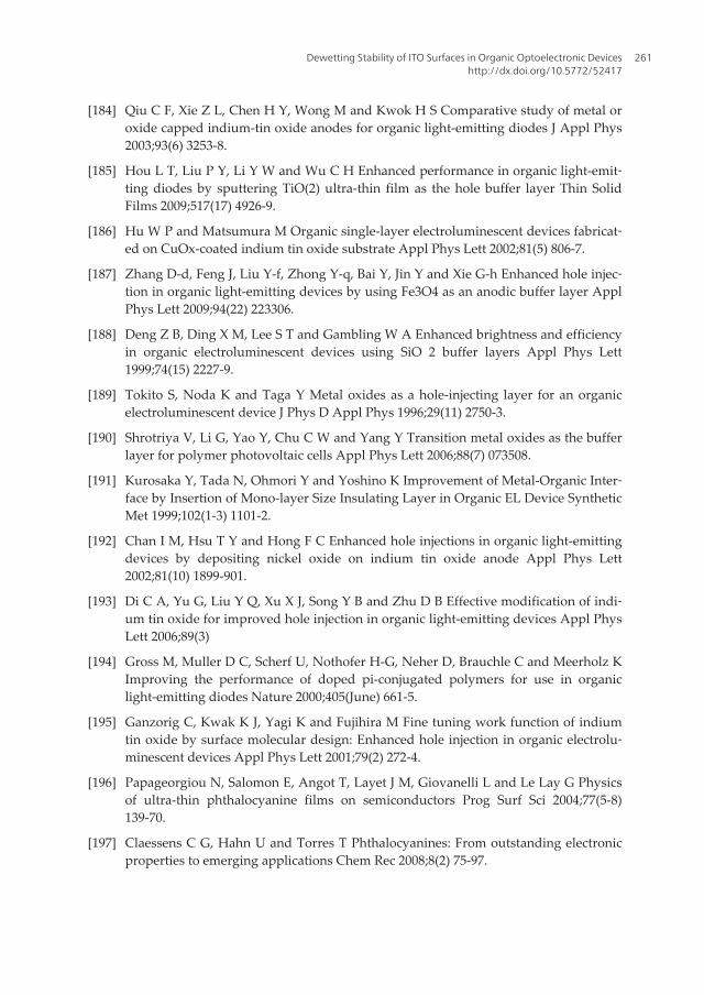
[184] Qiu C F, Xie Z L, Chen H Y, Wong M and Kwok H S Comparative study of metal oroxide capped indium-tin oxide anodes for organic light-emitting diodes J Appl Phys2003;93(6) 3253-8.
[185] Hou L T, Liu P Y, Li Y W and Wu C H Enhanced performance in organic light-emit‐ting diodes by sputtering TiO(2) ultra-thin film as the hole buffer layer Thin SolidFilms 2009;517(17) 4926-9.
[186] Hu W P and Matsumura M Organic single-layer electroluminescent devices fabricat‐ed on CuOx-coated indium tin oxide substrate Appl Phys Lett 2002;81(5) 806-7.
[187] Zhang D-d, Feng J, Liu Y-f, Zhong Y-q, Bai Y, Jin Y and Xie G-h Enhanced hole injec‐tion in organic light-emitting devices by using Fe3O4 as an anodic buffer layer ApplPhys Lett 2009;94(22) 223306.
[188] Deng Z B, Ding X M, Lee S T and Gambling W A Enhanced brightness and efficiencyin organic electroluminescent devices using SiO 2 buffer layers Appl Phys Lett1999;74(15) 2227-9.
[189] Tokito S, Noda K and Taga Y Metal oxides as a hole-injecting layer for an organicelectroluminescent device J Phys D Appl Phys 1996;29(11) 2750-3.
[190] Shrotriya V, Li G, Yao Y, Chu C W and Yang Y Transition metal oxides as the bufferlayer for polymer photovoltaic cells Appl Phys Lett 2006;88(7) 073508.
[191] Kurosaka Y, Tada N, Ohmori Y and Yoshino K Improvement of Metal-Organic Inter‐face by Insertion of Mono-layer Size Insulating Layer in Organic EL Device SyntheticMet 1999;102(1-3) 1101-2.
[192] Chan I M, Hsu T Y and Hong F C Enhanced hole injections in organic light-emittingdevices by depositing nickel oxide on indium tin oxide anode Appl Phys Lett2002;81(10) 1899-901.
[193] Di C A, Yu G, Liu Y Q, Xu X J, Song Y B and Zhu D B Effective modification of indi‐um tin oxide for improved hole injection in organic light-emitting devices Appl PhysLett 2006;89(3)
[194] Gross M, Muller D C, Scherf U, Nothofer H-G, Neher D, Brauchle C and Meerholz KImproving the performance of doped pi-conjugated polymers for use in organiclight-emitting diodes Nature 2000;405(June) 661-5.
[195] Ganzorig C, Kwak K J, Yagi K and Fujihira M Fine tuning work function of indiumtin oxide by surface molecular design: Enhanced hole injection in organic electrolu‐minescent devices Appl Phys Lett 2001;79(2) 272-4.
[196] Papageorgiou N, Salomon E, Angot T, Layet J M, Giovanelli L and Le Lay G Physicsof ultra-thin phthalocyanine films on semiconductors Prog Surf Sci 2004;77(5-8)139-70.
[197] Claessens C G, Hahn U and Torres T Phthalocyanines: From outstanding electronicproperties to emerging applications Chem Rec 2008;8(2) 75-97.
Dewetting Stability of ITO Surfaces in Organic Optoelectronic Deviceshttp://dx.doi.org/10.5772/52417
261
[198] de Oteyza D G, El-Sayed A, Garcia-Lastra J M, Goiri E, Krauss T N, Turak A, BarrenaE, Dosch H, Zegenhagen J, Rubio A, Wakayama Y and Ortega J E Copper-phthalo‐cyanine based metal-organic interfaces: The effect of fluorination, the substrate, andits symmetry J Chem Phys 2010;133(21)
[199] Scientific W 2012 Journal of Porphyrins and Phthalocyanines (JPP).
[200] Walter M G, Rudine A B and Wamser C C Porphyrins and phthalocyanines in solarphotovoltaic cells J Porphyr Phthalocya 2010;14(9) 759-92.
[201] Yu W L, Pei J, Cao Y and Huang W Hole-injection enhancement by copper phthalo‐cyanine (CuPc) in blue polymer light-emitting diodes J Appl Phys 2001;89(4) 2343-50.
[202] Kim S C, Lee G B, Choi M W, Roh Y, Whang C N, Jeong K, Lee J G and Kim S Con‐trolling hole injection in organic electroluminescent device by sputter-grown Cu-phthalocyanine thin films Appl Phys Lett 2001;78(10) 1445-7.
[203] Lee S T, Wang Y M, Hou X Y and Tang C W Interfacial electronic structures in anorganic light-emitting diode Appl Phys Lett 1999;74(5) 670-2.
[204] Fenenko L and Adachi C Influence of heat treatment on indium – tin-oxide anodesand copper phthalocyanine hole injection layers in organic light-emitting diodesThin Solid Films 2007;515(11) 4812-8.
[205] Tadayyon S M, Grandin H M, Griffiths K, Norton P R, Aziz H and Popovic Z D CuPcbuffer layer role in OLED performance: a study of the interfacial band energies OrgElectron 2004;5(4) 157-66.
[206] Mori T, Mitsuoka T, Ishii M, Fujikawa H and Taga Y Improving the thermal stabilityof organic light-emitting diodes by using a modified phthalocyanine layer Appl PhysLett 2002;80(21) 3895-7.
[207] Lobbert G 2000 Phthalocyanines. In: Ullmann's Encyclopedia of Industrial Chemis‐try, ed F Ullmann: Wiley-VCH Verlag)
[208] Lee Y J, Park S-s, Kim J and Kim H Interface morphologies and interlayer diffusionsin organic light emitting device by x-ray scattering Appl Phys Lett 2009;94(22)223305.
[209] Aziz H, Popovic Z D and Hu N-x Organic light emitting devices with enhanced op‐erational stability at elevated temperatures Appl Phys Lett 2002;81(2) 370-2.
[210] Choong V-e, Shen J, Curless J, Shi S and Yang J Efficient and durable organic alloysfor electroluminescent displays Journal of Physics D: Applied Physics 2000;33(7)760-3.
[211] Sheats J R, Antoniadis H, Hueschen M, Leonard W, Miller J, Moon R, Roitman D andStocking A Organic electroluminescent devices Science 1996;273(5277) 884-8.
Optoelectronics - Advanced Materials and Devices262
[212] dos Anjos P N M, Aziz H, Hu N X and Popovic Z D Temperature dependence ofelectroluminescence degradation in organic light emitting devices without and witha copper phthalocyanine buffer layer Org Electron 2002;3(1) 9-13.
[213] Cui J, Huang Q L, Veinot J G C, Yan H and Marks T J Interfacial microstructure func‐tion in organic light-emitting diodes: Assembled tetraaryldiamine and copper phtha‐locyanine interlayers Adv Mater 2002;14(8) 565-9.
[214] Peisert H, Knupfer M, Schwieger T and Fink J Strong chemical interaction betweenindium tin oxide and phthalocyanines Appl Phys Lett 2002;80(16) 2916-8.
[215] Kim J, Kim M, Kim J W, Yi Y and Kang H Organic light emitting diodes using NaCl:N ,N-bis(naphthalene-1-yl)- N , N-bis( phenyl) benzidine composite as a hole injec‐tion buffer layer J Appl Phys 2010;108(10) 103703.
[216] Aziz H and Popovic Z D Degradation Phenomena in Small-Molecule Organic Light-Emitting Devices Chem Mater 2004;16(23) 4522-32.
[217] Elschner A, Bruder F, Heuer H, Jonas F, Karbach A, Kirchmeyer S, Thrum S andWehrmann R PEDT:PSS for efficient hole-injection in hybrid organic light-emittingdiodes Synthetic Met 2000;111-112(1 June) 139-43.
[218] Matsushima T and Murata H Enhancing power conversion efficiencies and opera‐tional stability of organic light-emitting diodes by increasing carrier injection effi‐ciencies at anode / organic and organic / organic heterojunction interfaces Enhancingpower conversion efficiencies and J Appl Phys 2008;104(3) 034507.
[219] Cacialli F, Kim J S, Brown T M, Morgado J, Granstrom M, Friend R H, Gigli G, Cingo‐lani R, Favaretto L, Barbarella G, Daik R and Feast W J Surface and bulk phenomenain conjugated polymers devices Synthetic Met 2000;109(1-3) 7-11.
[220] Fukushi Y, Kominami H, Nakanishi Y and Hatanaka Y Effect of ITO surface state tothe aging characteristics of thin film OLED Appl Surf Sci 2005;244(1-4) 537-40.
[221] Mathai M K, Papadimitrakopoulos F and Hsieh B R Alq 3 -based organic light emit‐ting diodes to improve the device lifetime by an oxidized transport layer J Appl Phys2004;95(12) 8240-6.
[222] Chu T-y, Lee Y-h and Song O-k Effects of interfacial stability between electron trans‐porting layer and cathode on the degradation process of organic light-emitting di‐odes Appl Phys Lett 2007;91(22) 223509.
[223] Liew Y-f, Zhu F, Chua S-j and Tang J-x Tris-(8-hydroxyquinoline)aluminum-modi‐fied indium tin oxide for enhancing the efficiency and reliability of organic light-emitting devices Appl Phys Lett 2004;85(19) 4511-3.
[224] Chwang A B, Kwong R C and Brown J J Graded mixed-layer organic light-emittingdevices Appl Phys Lett 2002;80(5) 725-7.
Dewetting Stability of ITO Surfaces in Organic Optoelectronic Deviceshttp://dx.doi.org/10.5772/52417
263
[225] Lee M-t, Liao C-h and Tsai C-h Improved stability of organic electroluminescent de‐vices by doping styrylamines in hole or electron transporting layer Appl Phys Lett2005;86(10) 103501.
[226] Tsai C-h, Liao C-h, Lee M-t and Chen C H Highly stable organic light-emitting devi‐ces with a uniformly mixed hole transport layer Appl Phys Lett 2005;87(24) 243505.
[227] Lee T-w, Kwon O, Kim M-g, Park S H, Chung J, Kim S Y, Chung Y, Park J-Y, Han E,Huh D H, Park J-J and Pu L Hole-injecting conducting-polymer compositions forhighly efficient and stable organic light-emitting diodes Appl Phys Lett 2005;87(23)231106.
[228] Jung G Y, Yates A, Samuel I D W and Petty M C Lifetime studies of light-emittingdiode structures incorporating polymeric Langmuir – Blodgett films Materials Sci‐ence and Engineering C 2001;14(1-2) 1-10.
[229] Kim J, Lee J, Han C W, Lee N Y and Chung I J Effect of thermal annealing on thelifetime of polymer light-emitting diodes Appl Phys Lett 2003;82(24) 4238-40.
[230] Voroshazi E, Verreet B, Buri A, Muller R, Di Nuzzo D and Heremans P Influence ofcathode oxidation via the hole extraction layer in polymer:fullerene solar cells OrgElectron 2011;12(5) 736-44.
[231] Sun Y M, Takacs C J, Cowan S R, Seo J H, Gong X, Roy A and Heeger A J Efficient,Air-Stable Bulk Heterojunction Polymer Solar Cells Using MoOx as the Anode Inter‐facial Layer Adv Mater 2011;23(19) 2226-30.
[232] Zilberberg K, Gharbi H, Behrendt A, Trost S and Riedl T Low-Temperature, Solution-Processed MoOx for Efficient and Stable Organic Solar Cells ACS Appl Mater Inter2012;4(3) 1164-8.
[233] Kim Y H, Sachse C, Hermenau M, Fehse K, Riede M, Muller-Meskamp L and Leo KImproved efficiency and lifetime in small molecule organic solar cells with optimizedconductive polymer electrodes Appl Phys Lett 2011;99(11) 113305.
[234] Kirchmeyer S and Reuter K Scientific importance, properties and growing applica‐tions of poly( 3,4-ethylenedioxythiophene) J Mater Chem 2005;15(21) 2077-88.
[235] Carter J C, Grizzi I, Heeks S K, Lacey D J, Latham S G, May P G, Los O R D, PichlerK, Towns C R and Wittmann H F Operating stability of light-emitting polymer di‐odes based on poly ( p -phenylene vinylene ) Appl Phys Lett 1997;71(1) 34-6.
[236] Jonda C, Mayer A B R, Stolz U, Elschner A and Karbach A Surface roughness effectsand their influence on the degradation of organic light emitting devices J Mater Sci2000;35(22) 5645-51.
[237] Stephan O, Tran-van F and Chevrot C New organic materials for light emitting devi‐ces based on dihexylfluorene-co-ethylenedioxythiophene copolymers exhibiting im‐proved hole-injecting properties Synthetic Met 2002;131(1-3) 31-40.
Optoelectronics - Advanced Materials and Devices264
[238] Maye F. Morphological and structural study of ultrathin lithium floride films on or‐ganic molecule surfaces.Doctorate thesis.University of Stuttgart;2011.
[239] Kawano K, Pacios R, Poplavskyy D, Nelson J, Bradley D D C and Durrant J R Degra‐dation of organic solar cells due to air exposure Sol Energ Mat Sol C 2006;90(20)3520-30.
[240] Sharma A, Andersson G and Lewis D A Role of humidity on indium and tin migra‐tion in organic photovoltaic devices Phys Chem Chem Phys 2011;13(10) 4381-7.
[241] Nguyen T P, Le Rendu P, Long P D and De Vos S A Chemical and thermal treatmentof PEDOT: PSS thin films for use in organic light emitting diodes Surf Coat Tech2004;180-181(1 March) 646-9.
[242] Bulle-Lieuwma C W T, van Gennip W J H, van Duren J K J, Jonkheijm P, Janssen R AJ and Niemantsverdriet J W Characterization of polymer solar cells by TOF-SIMSdepth profiling Appl Surf Sci 2003;203-204(15 Jan) 547-50.
[243] Huang J, Miller P F, Wilson J S, Mello A J D, Mello J C D and Bradley D D C Investi‐gation of the Effects of Doping and Post-Deposition Treatments on the Conductivity ,Morphology , and Work Function of Poly ( 3 , 4-ethylenedioxythiophene )/ Poly( styrene sulfonate ) Films Adv Funct Mater 2005;15(2) 290-6.
[244] Norrman K, Madsen M V, Gevorgyan S A and Krebs F C Degradation Patterns inWater and Oxygen of an Inverted Polymer Solar Cell J Am Chem Soc 2010;132(47)16883-92.
[245] Moujoud A, Oh S H, Hye J J, Jae H and Kim H J C61-butyric acid methyl ester bulkheterojunction solar cell by using UV light irradiation Solar Energy Materials and So‐lar Cells 2011;95(4) 1037-41.
[246] Arora S, Rajouria S K, Kumar P and Bhatnagar P K Role of donor – acceptor domainformation and interface states in initial degradation of P3HT: PCBM-based solar cellsPhys. Scr. 2011;83(3) 035804.
[247] Norrman K, Larsen N B and Krebs F C Lifetimes of organic photovoltaics: Combin‐ing chemical and physical characterisation techniques to study degradation mecha‐nisms Sol Energ Mat Sol C 2006;90(17) 2793-814.
[248] Archambeau S, Seguy I, Jolinat P, Farenc J, Destruel P, Nguyen T P, Bock H and Gre‐let E Stabilization of discotic liquid organic thin films by ITO surface treatment ApplSurf Sci 2006;253(4) 2078-86.
[249] Chen C Y, Wu K Y, Chao Y C, Zan H W, Meng H F and Tao Y T Concomitant tuningof metal work function and wetting property with mixed self-assembled monolayersOrg Electron 2011;12(1) 148-53.
[250] Cui J, Huang Q, Wang Q and Marks T J Enhancing Anode / Hole-Transport LayerInterfacial Light-Emitting Diodes Langmuir 2001;17(7) 2051-4.
Dewetting Stability of ITO Surfaces in Organic Optoelectronic Deviceshttp://dx.doi.org/10.5772/52417
265

[251] Kacker N, Kumar S K and Allara D L Wetting-induced reconstruction in molecularsurfaces Langmuir 1997;13(24) 6366-9.
[252] Hayakawa R, Turak A, Zhang X, Hiroshiba N, Dosch H, Chikyow T and WakayamaY Strain-effect for controlled growth mode and well-ordered structure of quaterry‐lene thin films J Chem Phys 2010;133(3) 034706.
[253] Han E-m, Do L-m, Fujihira M, Inada H and Shirota Y Scanning force microscopy oforganic thin-film amorphous hole transport materials J Appl Phys 1996;80(6) 3297-9.
[254] Ke L, Senthil R, Zhang K, Jin S and Wee A T S Organic light emitting devices per‐formance improvement by inserting thin parylene layer Synthetic Met 2004;140(2-3)295-9.
[255] Hains A W, Chen H-y, Reilly T H and Gregg B A Cross-Linked Perylene Diimide-Based n-Type Interfacial Layer for Inverted Organic Photovoltaic Devices ACS ApplMater Inter 2011;3(11) 4381-7.
[256] Madsen M V, Krebs F C, Madsen M V, Norrman K and Krebs F C Oxygen- and wa‐ter-induced degradation of an inverted polymer solar cell: the barrier effect Journalof Photonics for Energy 2011;1(1) 011104.
[257] Vestweber H and Riels W Highly efficient and stable organic light-emitting SyntheticMet 1997;91(97) 181-5.
[258] Han E M, Do L M, Yamamoto N and Fujihira M Crystallization of organic thin filmsfor electroluminescent devices Thin Solid Films 1996;273(1-2) 202-8.
[259] Camaioni N, Ridolfi G, Casalbore-Miceli G, Possamai G, Garlaschelli L and MagginiM A stabilization effect of [60]fullerene in donor-acceptor organic solar cells Sol En‐erg Mat Sol C 2003;76(1) 107-13.
[260] Neugebauer H, Brabec C, Hummelen J C and Sariciftci N S Stability and photodegra‐dation mechanisms of conjugated polymer/fullerene plastic solar cells Sol Energ MatSol C 2000;61(1) 35-42.
[261] Lee J U, Jung J W, Emrick T, Russell T P and Jo W H Synthesis of C(60)-end cappedP3HT and its application for high performance of P3HT/PCBM bulk heterojunctionsolar cells J Mater Chem 2010;20(16) 3287-94.
[262] Lee J U, Jung J W, Emrick T, Russell T P and Jo W H Morphology control of a poly‐thiophene-fullerene bulk heterojunction for enhancement of the high-temperaturestability of solar cell performance by a new donor-acceptor diblock copolymer Nano‐technology 2010;21(10) 105201.
[263] Santerre F, Bedja I, Dodelet J P, Sun Y, Lu J, Hay A S and D'Iorio M Hole transportmolecules in high T-g polymers: Their effect on the performance of organic light-emitting diodes Chem Mater 2001;13(5) 1739-45.
[264] Shi J M and Tang C W Doped organic electroluminescent devices with improved sta‐bility Appl Phys Lett 1997;70(13) 1665-7.
Optoelectronics - Advanced Materials and Devices266

[265] Jarikov V V Improving operating lifetime of organic light-emitting diodes with poly‐cyclic aromatic hydrocarbons as aggregating light-emitting-layer additives J ApplPhys 2006;100(1) 014901.
[266] Jarikov V V, Young R H, Vargas J R, Brown C T, Klubek K P and Liao L-s Operatinglongevity of organic light-emitting diodes with perylene derivatives as aggregatinglight-emitting-layer additives: Expansion of the emission zone J Appl Phys2006;100(9) 094907.
[267] Fong H H, Choy W C H, Hui K N and Liang Y J Organic light-emitting diodes basedon a cohost electron transporting composite Appl Phys Lett 2006;88(11) 113510.
[268] Meerheim R, Walzer K, Pfeiffer M and Leo K Ultrastable and efficient red organiclight emitting diodes with doped transport layers Appl Phys Lett 2006;89(6) 061111.
[269] Yuan Y, Grozea D and Lu Z H Fullerene-doped hole transport molecular films fororganic light-emitting diodes Appl Phys Lett 2005;86(14) 143509.
[270] Yuan Y Y, Han S, Grozea D and Lu Z H Fullerene-organic nanocomposite: A flexiblematerial platform for organic light-emitting diodes Appl Phys Lett 2006;88(9) 093503.
[271] Holmes M A, Mackay M E and Giunta R K Nanoparticles for dewetting suppressionof thin polymer films used in chemical sensors Journal of Nanoparticle Research2007;9(5) 753-63.
[272] Ling G P and He J H The influence of nano-Al2O3 additive on the adhesion betweenenamel and steel substrate Mat Sci Eng a-Struct 2004;379(1-2) 432-6.
[273] Hsu S H, Chou C W and Tseng S M Enhanced thermal and mechanical properties inpolyurethane/Au nanocomposites Macromol Mater Eng 2004;289(12) 1096-101.
[274] Sharma S, Rafailovich M H, Peiffer D and Sokolov J Control of Dewetting Dynamicsby Adding Nanoparticle Fillers Nano letters 2001;1(10) 511-4.
[275] Luo H and Gersappe D Dewetting Dynamics of Nanofilled Polymer Thin Films Mac‐romolecules 2004;37(15) 5792-9.
[276] Hains A W, Liu J, Martinson A B F, Irwin M D and Marks T J Anode Interfacial Tun‐ing via Electron-Blocking / Hole- Transport Layers and Indium Tin Oxide SurfaceTreatment in Bulk-Heterojunction Organic Photovoltaic Cells Adv Funct Mater2010;20(4) 595-606.
[277] Hains A W and Marks T J High-efficiency hole extraction / electron-blocking layer toreplace heterojunction polymer solar cells Appl Phys Lett 2008;92(2) 023504.
[278] Hains A W, Ramanan C, Irwin M D, Liu J, Wasielewski M R and Marks T J DesignedBithiophene-Based Interfacial Layer for High-Efficiency Bulk-Heterojunction OrganicPhotovoltaic Cells. Importance of Interfacial Energy Level Matching ACS Appl MaterInter 2010;2(1) 175-85.
Dewetting Stability of ITO Surfaces in Organic Optoelectronic Deviceshttp://dx.doi.org/10.5772/52417
267
[279] Cahen D and Hodes G Molecules and electronic materials Adv Mater 2002;14(11)789-98.
[280] Bellmann E, Jabbour G E and Grubbs R H Hole Transport Polymers with ImprovedInterfacial Contact to the Anode Material Chem Mater 2000;12(8) 1349-53.
[281] Mori T, Miyake S and Mizutani T Effects of Plasma Modification on Hole TransportLayer in Organic Electroluminescent Diode Jpn J Appl Phys 2 1995;34(7A) L845-L8.
[282] Han E M, Yun J J, Oh G C, Park S M, Park N K, Yoon Y S and Fujihira M Enhancedstability of organic thin films for electroluminescence by photoirradiation OpticalMaterials 2002;21(1-3) 243-8.
[283] Sun Y, Chien S-c, Yip H-l, Zhang Y, Chen K-s, Zeigler D F, Chen F-c, Lin B and Jen AK Chemically Doped and Cross-linked Hole-Transporting Materials as an EfficientAnode Buffer Layer for Polymer Solar Cells Chem Mater 2011;23(22) 5006-15.
[284] Chan M Y, Lai S L, Wong F L, Lengyel O, Lee C S and Lee S T Efficiency enhance‐ment and retarded dark-spots growth of organic light-emitting devices by high-tem‐perature processing Chem Phys Lett 2003;371(5-6) 700-6.
[285] Chin B D, Duan L, Kim M-h, Lee S T and Chung H K Effects of cathode thickness andthermal treatment on the design of balanced blue light-emitting polymer device ApplPhys Lett 2004;85(19) 4496-8.
[286] Fenwick O, Oliver K and Cacialli F Cross-linking of a poly(3,4-ethylene dioxythio‐phene):(polystyrene sulfonic acid) hole injection layer with a bis-azide salt and the ef‐fect of atmospheric processing conditions on device properties Appl Phys Lett2012;100(5) 053309.
[287] Ryu S Y, Kim J T, Noh J H, Hwang B H, Kim C S, Jo S J, Hwang H S, Kang S J, Baik HK, Lee C H, Song S Y and Lee S J Polymeric tandem organic light-emitting diodes us‐ing a self-organized interfacial layer Appl Phys Lett 2008;92(10) 103301.
[288] Wang J Z, Zheng Z H, Li H W, Huck W T S and Sirringshaus H Polymer field effecttransistors fabricated by dewetting Synthetic Met 2004;146(3) 287-90.
[289] Benor A, Hoppe A, Wagner V and Knipp D Microcontact printing and selective sur‐face dewetting for large area electronic applications Thin Solid Films 2007;515(19)7679-82.
[290] Harirchian-Saei S, Wang M C P, Gates B D and Moffitt M G Directed Polystyrene/Poly(methyl methacrylate) Phase Separation and Nanoparticle Ordering on Trans‐parent Chemically Patterned Substrates Langmuir 2012;28(29) 10838-48.
Optoelectronics - Advanced Materials and Devices268


![Thickness-dependent spontaneous dewetting morphology of ...people.wku.edu/mikhail.khenner/LaserPattAg.pdfheterogeneous nucleation or spinodal dewetting [23]. In the case of homogeneous](https://img.pdfslide.us/doc/110x75/60ee61d71c1e3b20b84c0cd4/thickness-dependent-spontaneous-dewetting-morphology-of-heterogeneous-nucleation.jpg)