Embed Size (px)
Citation preview
Device manual
ioControl CR2050 CR2051 CR2052
8026
8387
/ 00
12
/ 20
19
UK
Original Scale Drawing (MTD)P_MZ_e100_0092
EPS SourceProduct Scale DrawingFrame Size: 80 mm x 90 mm
30% 333,4%
1 2
4
6
8
3
5
7
205,
523
4,2
76
52
17
6,9
8,7
6,9
1
2
3
27,411
40,5
4
5
ioControl
2
Contents1 Preliminary note 4
11 Explanation of symbols 42 Safety instructions 53 Functions and features 64 Function 75 Installation 7
51 Installation location 752 Mounting surface 753 Heat dissipation 854 Fastening 855 Cable seal 9
6 Electrical connection 961 Wiring 962 General wiring information 1063 Connection technology 1164 Connection accessories 1165 Frequency inputs 1166 Reverse polarity protection 1167 Supply of the signal generators at the inputs 1268 Fuses 1269 Examples for connection types 13
691 CR2050 13692 CR2051 14693 CR2052 15
7 Operating and display elements 1671 Menu structure 1772 Status indication of the inputs/outputs (I/O LEDs, yellow) 18
8 Set-up 1981 I/O module 19
811 Display mode 19812 Parameter setting 19813 List of parameters 20
82 Controller 21821 Programming 21
83 Required documentation 2184 Required hardware 21
9 Technical data 2291 CR2050 2292 CR2051 2993 CR2052 36
UK
ioControl
3
This document is the original instructions All trademarks and company names used are subject to the copyright of the respective companies
10 Maintenance, repair and disposal 4411 Approvals/standards 4412 Appendix 45
121 EMCY Object 45122 Object directory CR205x 45
1221 Device-specific CR2050 491222 Device-specific CR2051 701223 Device-specific CR2052 94
123 SDOs error messages 1261231 CR2050 1261232 CR2051 1281233 CR2052 130
ioControl
4
1 Preliminary noteTechnical data, approvals, accessories and further information at wwwifmcom
1.1 Explanation of symbols
Instructions> Reaction, result[…] Designation of keys, buttons or indications→ Cross-reference
Important note Non-compliance may result in malfunction or interferenceInformation Supplementary note
WARNING!Warning of serious personal injury Death or serious irreversible injuries may result
CAUTION!Warning of personal injury Slight reversible injuries may result
NOTE!Warning of damage to property
UK
ioControl
5
2 Safety instructions The device described is a subcomponent for integration into a system
The manufacturer is responsible for the safety of the system The system manufacturer undertakes to perform a risk assessment and to create documentation in accordance with legal and normative requirements to be provided to the operator and user of the system This documentation must contain all necessary information and safety instructions for the operator, the user and, if applicable, for any service personnel authorised by the manufacturer of the system
Read this document before setting up the product and keep it during the entire service life
The product must be suitable for the corresponding applications and environmental conditions without any restrictions
Only use the product for its intended purpose (→ 3 Functions and features) If the operating instructions or the technical data are not adhered to, personal
injury and/or damage to property may occur In case of malfunctions, please contact the manufacturer Tampering with the
unit is not allowed Installation, electrical connection, set-up, programming, configuration,
operation and maintenance of the product must be carried out by personnel qualified and authorised for the respective activity
Protect units, connectors and cables against damage Replace damaged units, since otherwise the technical data and safety will be
impaired
Gaps of different widths may be present at the bottom of the unit These do not affect the functions of the unit
ioControl
6
NOTE!Excessive current, weld slag and soiling due to welding
> Damage to the device, deterioration of the electrical safety Welding work on the chassis frame must only be carried out by qualified personnel
Remove and cover the plus and minus terminals of the batteries Disconnect all contacts of the device from the on-board system prior to welding on the vehicle or machine
Connect the earth terminal of the welding device directly to the part to be welded
Do not touch the device or electric cables with the welding electrode or the earth terminal of the welding device
Protect the device incl all connectors and all connection cables against weld slag and soiling
3 Functions and featuresThe freely programmable controllers of the "ioControl" series are rated for use under difficult conditions: This includes an extended temperature range, strong vibration, intensive EMC interferences and wet environmentsBy means of the application software the user can configure the inputs and outputs to adapt to the respective application The controllers can be used as CANopen device, master or intelligent I/O module (→ 9 Technical data)Application-specific extensions and adaptations are possible in conjunction with additional products of the modular ioControl and Basic series
WARNING!Deterioration of the safety function
> Possible hazard for people or installationsThe device is not approved for safety-related tasks in the field of operator protection
Only use the device within the limits of the technical data (→ 9 Technical data)
UK
ioControl
7
4 Function The user can easily create the application software by means of the IEC 61131-
3 compliant programming system CODESYS 23 On delivery the devices are pre-configured as CANopen device
2 CAN interfaces configurable inputs/outputs status LEDs, I/O LEDs and 4-digit 10-segment display operating keys
More information and accessories at wwwifmcom
5 Installation5.1 Installation locationThe following installation locations are permitted:
inside of the cabin body vehicle frame
Installation on the motor/engine is not permittedFor non-mobile applications, the applicable directives are to be adhered to, taking into account the specified environmental conditions
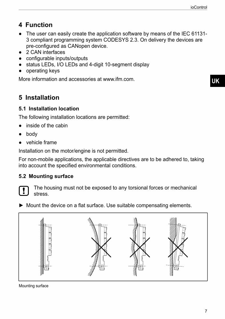
5.2 Mounting surface
The housing must not be exposed to any torsional forces or mechanical stress
Mount the device on a flat surface Use suitable compensating elements
Mounting surface
ioControl
8
5.3 Heat dissipation
CAUTION!The housing can heat up considerably
> Risk of burns During installation, ensure sufficient heat dissipation Measure maximum device heating in the application The maximum housing temperature indicated in the data sheet must not be exceeded
If housing temperatures presenting a danger to people are reached: Cover housing to prevent unintentional contact Apply warning for hot surfaces visibly on the device
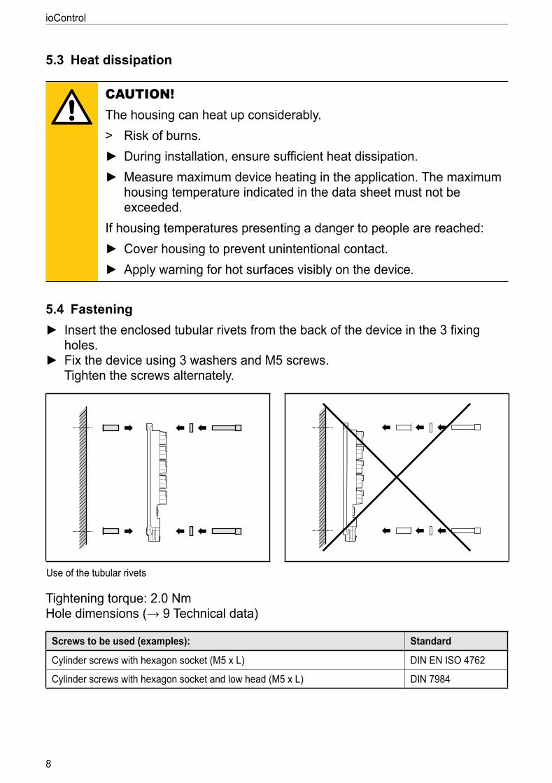
5.4 Fastening Insert the enclosed tubular rivets from the back of the device in the 3 fixing holes
Fix the device using 3 washers and M5 screws Tighten the screws alternately
Use of the tubular rivets
Tightening torque: 20 NmHole dimensions (→ 9 Technical data)
Screws to be used (examples): Standard
Cylinder screws with hexagon socket (M5 x L) DIN EN ISO 4762
Cylinder screws with hexagon socket and low head (M5 x L) DIN 7984
UK
ioControl
9
5.5 Cable seal
Before and during installation, observe the pollution degree (→ 9 Technical data) until the protection rating is ensured by means of connectors/dummy plugs Protection rating IP 65 / IP 67 is only guaranteed if all ports are sealed by means of connectors or dummy plugs
In case of high humidity, only mount the unit on a vertical surface
If the modules are subjected to increased environmental requirements, the use of connectors with the sealing geometry of the "enhanced seal retention" series from Deutsch or Amphenol is recommended
6 Electrical connection Disconnect the machine from the mains supply before installation; if necessary, also disconnect any independently supplied input / output load circuits
Observe the national and international regulations for the installation of electrical equipment
Observe the requirements according to IEC 60204
Accessible surfaces of the device are insulated from the circuits with basic insulation to IEC 61010-1 (secondary circuit with max 32 V DC, supplied from the mains circuit up to 300 V of overvoltage category II)The external wiring has to be carried out in a way that ensures the required separation from other circuits
6.1 WiringWiring (→ 9 Technical data)
The connection terminals may only be supplied with the signals indicated in the technical data / on the device label and only the approved accessories from ifm electronic gmbh may be connected
The device is designed for supply via a mobile on-board system (12/24 V DC nominal voltage) or SELV/PELV according to the technical data and national regulations The supply is directly transferred to the connected sensors/actuators without electrical separation
ioControl
10
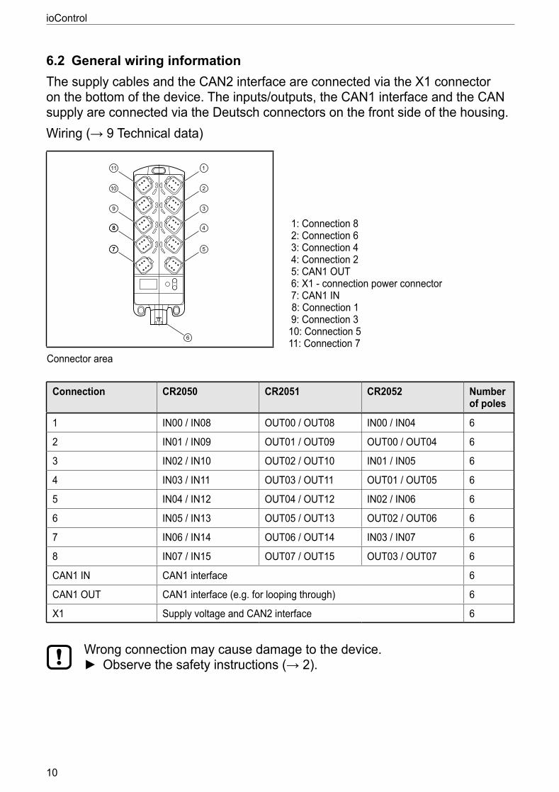
6.2 General wiring information The supply cables and the CAN2 interface are connected via the X1 connector on the bottom of the device The inputs/outputs, the CAN1 interface and the CAN supply are connected via the Deutsch connectors on the front side of the housingWiring (→ 9 Technical data)
Original Scale Drawing (MTD)P_MZ_e100_0092
EPS SourceProduct Scale DrawingFrame Size: 80 mm x ... mm
30% 333,4%
1
3
5
6
7
2
48
7
8
9
10
11
1: Connection 8 2: Connection 6 3: Connection 4 4: Connection 2 5: CAN1 OUT 6: X1 - connection power connector 7: CAN1 IN
8: Connection 1 9: Connection 3 10: Connection 5 11: Connection 7
Connector area
Connection CR2050 CR2051 CR2052 Number of poles
1 IN00 / IN08 OUT00 / OUT08 IN00 / IN04 6
2 IN01 / IN09 OUT01 / OUT09 OUT00 / OUT04 6
3 IN02 / IN10 OUT02 / OUT10 IN01 / IN05 6
4 IN03 / IN11 OUT03 / OUT11 OUT01 / OUT05 6
5 IN04 / IN12 OUT04 / OUT12 IN02 / IN06 6
6 IN05 / IN13 OUT05 / OUT13 OUT02 / OUT06 6
7 IN06 / IN14 OUT06 / OUT14 IN03 / IN07 6
8 IN07 / IN15 OUT07 / OUT15 OUT03 / OUT07 6
CAN1 IN CAN1 interface 6
CAN1 OUT CAN1 interface (eg for looping through) 6
X1 Supply voltage and CAN2 interface 6
Wrong connection may cause damage to the device Observe the safety instructions (→ 2)
UK
ioControl
11
6.3 Connection technology Basically lay all supply and signal cables separately Lay supply and signal cables away from the device using the shortest possible route
Note the device label Use twisted-pair cables for the CAN connection Provide all outgoing cables with a strain relief 400 mm behind the cable entry Cover unused sockets with dummy plugs
6.4 Connection accessoriesInformation about the available accessories at wwwifmcom
6.5 Frequency inputsCR2050 / CR2052:
Operate frequency inputs with screened cables so that useful signals are not affected by external interference
6.6 Reverse polarity protection
NOTE!Absence of reverse polarity protectionReverse polarity protection is only ensured in case of supply via the on-board system (via a battery), if the polarity of the supply is reversed as a whole (battery connected incorrectly) The basic principle of the reverse polarity protection is that upstream fuses will quickly switch off in case of excessive current caused by reverse polarity In case of supply via SELV/PELV, reverse polarity protection is not ensured
> Damage to the device Potential fire hazard
Ensure that the ends of the cables are properly connected to the connector before connecting the latter to the device, also in case of supply via the on-board system
CR2051: There is no reverse polarity protection of the CAN supply voltage, as this voltage is not used within the device
ioControl
12
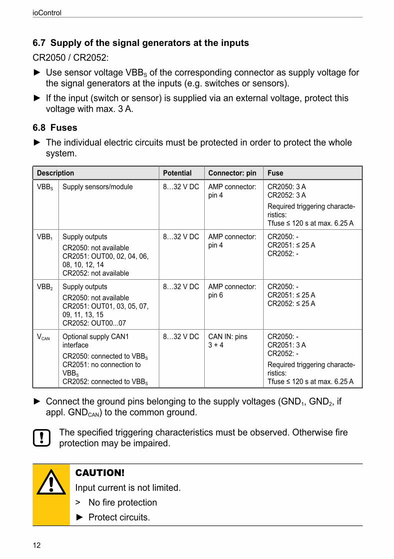
6.7 Supply of the signal generators at the inputsCR2050 / CR2052:
Use sensor voltage VBBS of the corresponding connector as supply voltage for the signal generators at the inputs (eg switches or sensors)
If the input (switch or sensor) is supplied via an external voltage, protect this voltage with max 3 A
6.8 Fuses The individual electric circuits must be protected in order to protect the whole system
Description Potential Connector: pin Fuse
VBBS Supply sensors/module 8…32 V DC AMP connector: pin 4
CR2050: 3 A CR2052: 3 ARequired triggering characte-ristics: Tfuse ≤ 120 s at max. 6.25 A
VBB1 Supply outputsCR2050: not available CR2051: OUT00, 02, 04, 06, 08, 10, 12, 14 CR2052: not available
8…32 V DC AMP connector: pin 4
CR2050: - CR2051: ≤ 25 A CR2052: -
VBB2 Supply outputsCR2050: not available CR2051: OUT01, 03, 05, 07, 09, 11, 13, 15 CR2052: OUT0007
8…32 V DC AMP connector: pin 6
CR2050: - CR2051: ≤ 25 A CR2052: ≤ 25 A
VCAN Optional supply CAN1 interfaceCR2050: connected to VBBS CR2051: no connection to VBBS CR2052: connected to VBBS
8…32 V DC CAN IN: pins 3 + 4
CR2050: - CR2051: 3 A CR2052: -Required triggering characte-ristics: Tfuse ≤ 120 s at max. 6.25 A
Connect the ground pins belonging to the supply voltages (GND1, GND2, if appl GNDCAN) to the common ground
The specified triggering characteristics must be observed Otherwise fire protection may be impaired
CAUTION!Input current is not limited
> No fire protection Protect circuits
UK
ioControl
13
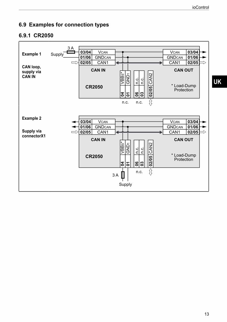
6.9 Examples for connection types
6.9.1 CR2050
Example 1
CAN loop, supply via CAN IN
CR2050 * Load-DumpProtection
CAN IN CAN OUT
03/04 VCAN
02/05 CAN1
Supply3 A
n.c. n.c.
01/06 GNDCAN
VB
BS*
06
GN
D1
n.c.
0104
03/04VCAN
CAN1GNDCAN
03n.
c.
02/0
5C
AN
2
02/0501/06
CR2050 * Load-DumpProtection
CAN IN CAN OUT
03/04 VCAN
02/05 CAN1
Supply
3 An.c.
01/06 GNDCAN
VB
BS*
06
GN
D1
n.c.
010403/04VCAN
CAN1GNDCAN
03n.
c.
02/0
5C
AN
2
02/0501/06
Example 2
Supply via connectorX1
ioControl
14
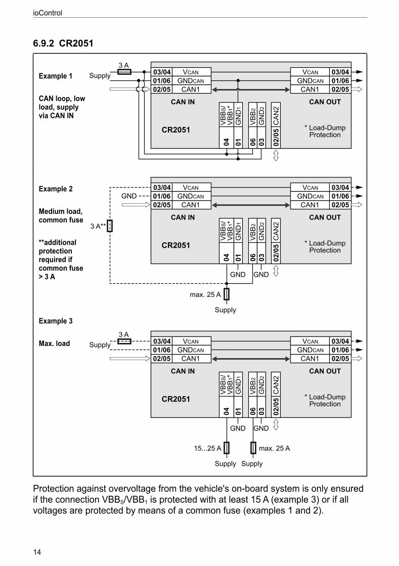
6.9.2 CR2051
Example 1
CAN loop, low load, supply via CAN IN
CR2051 * Load-DumpProtection
CAN IN CAN OUT
03/04 VCAN
02/05 CAN1
Supply3 A
01/06 GNDCAN
VB
BS/
VB
B1 *
06
GN
D1
VB
B2
GN
D2
0104
03/04VCAN
CAN1GNDCAN
03 02/0
5C
AN
2
Supply3 A
02/0501/06
Supply
max. 25 A
3 A**
CR2051 * Load-DumpProtection
CAN IN CAN OUT
03/04 VCAN
02/05 CAN101/06 GNDCAN
VB
BS/
VB
B1 *
06
GN
D1
VB
B2
GN
D2
0104
03/04VCAN
CAN1GNDCAN
03 02/0
5C
AN
2
02/0501/06
GND
GND
GND
Supply
15...25 A
Supply
max. 25 A
CR2051 * Load-DumpProtection
CAN IN CAN OUT
03/04 VCAN
02/05 CAN101/06 GNDCAN
VB
BS/
VB
B1 *
06
GN
D1
VB
B2
GN
D2
0104
03/04VCAN
CAN1GNDCAN
03 02/0
5C
AN
2
02/0501/06
GND GND
Example 2
Medium load, common fuse
**additional protection required if common fuse > 3 A
Example 3
Max. load
Protection against overvoltage from the vehicle's on-board system is only ensured if the connection VBBS/VBB1 is protected with at least 15 A (example 3) or if all voltages are protected by means of a common fuse (examples 1 and 2)
UK
ioControl
15
6.9.3 CR2052
Example 1
CAN loop, low load, supply via CAN IN
Supply3 A
CR2052 * Load-DumpProtection
CAN IN CAN OUT
03/04 VCAN
02/05 CAN101/06 GNDCAN
VB
BS
06
GN
D1
VB
B2 *
0104
03/04VCAN
CAN1GNDCAN
03G
ND
2
02/0
5C
AN
2
02/0501/06
CR2052 * Load-DumpProtection
CAN IN CAN OUT
03/04 VCAN
02/05 CAN101/06 GNDCAN
VB
BS
06
GN
D1
VB
B2 *
0104
03/04VCAN
CAN1GNDCAN
03G
ND
2
02/0
5C
AN
2
02/0501/06
Supply
3 A
GND GND
CR2052 * Load-DumpProtection
CAN IN CAN OUT
03/04 VCAN
02/05 CAN101/06 GNDCAN
VB
BS
06
GN
D1
VB
B2 *
0104
03/04VCAN
CAN1GNDCAN
03G
ND
2
02/0
5C
AN
2
02/0501/06
3 A
Supply
15...25 A
GND GND
Supply
Example 2
low load, common fuse
Example 3
max. load
Protection against overvoltage from the vehicle's on-board system is only ensured if the connection VBB2 is protected with at least 15 A (example 3) or if all voltages are protected by means of a common fuse (examples 1 and 2)
ioControl
16
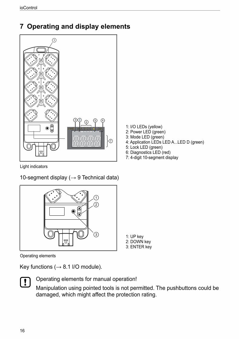
7 Operating and display elementsOriginal Scale Drawing (MTD)P_MZ_e100_0092
EPS SourceProduct Scale DrawingFrame Size: 80 mm x 90 mm
30% 333,4%
1 2
4
6
8
3
5
7
205,
523
4,2
76
52
17
6,9
8,7
6,9
1
2
3
27,411
40,5
4
5
1 2
4
6
8
3
5
7
1
1: I/O LEDs (yellow) 2: Power LED (green) 3: Mode LED (green) 4: Application LEDs LED ALED D (green) 5: Lock LED (green) 6: Diagnostics LED (red) 7: 4-digit 10-segment display
Light indicators
10-segment display (→ 9 Technical data)
Original Scale Drawing (MTD)P_MZ_e100_0092
EPS SourceProduct Scale DrawingFrame Size: 80 mm x 90 mm
30% 333,4%
1
2
3
1 2
4
6
8
3
5
7
205,
523
4,2
76
52
17
6,9
8,7
6,9
1
2
3
27,411
40,5
4
5
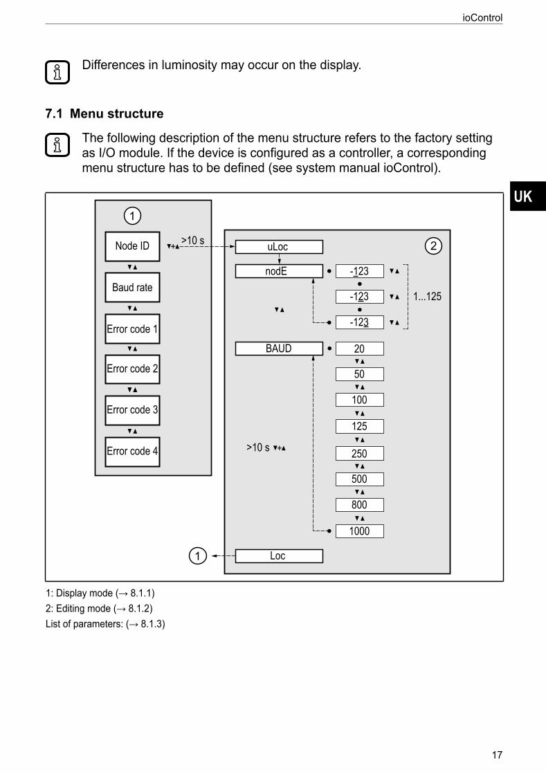
1: UP key 2: DOWN key 3: ENTER key
Operating elements
Key functions (→ 8.1 I/O module)
Operating elements for manual operation!Manipulation using pointed tools is not permitted The pushbuttons could be damaged, which might affect the protection rating
UK
ioControl
17
Differences in luminosity may occur on the display
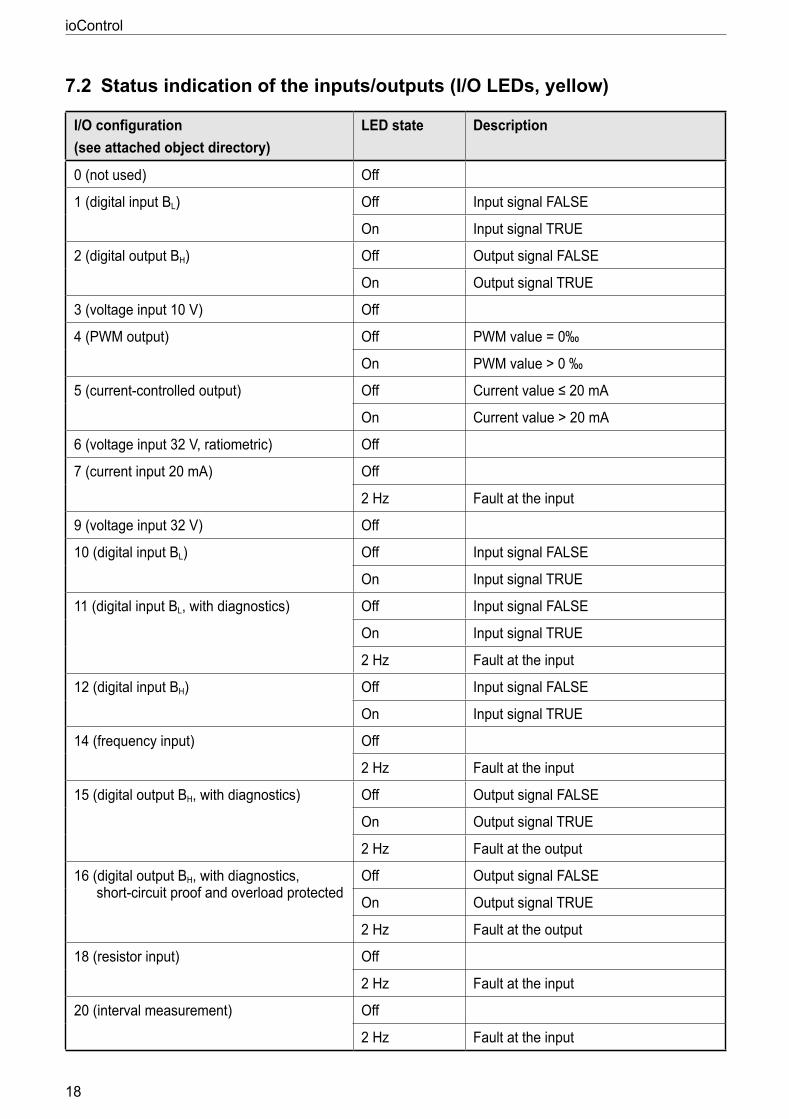
7.1 Menu structure
The following description of the menu structure refers to the factory setting as I/O module If the device is configured as a controller, a corresponding menu structure has to be defined (see system manual ioControl)
Node ID uLoc
Loc
nodE -123
1
1
BAUD
Baud rate
Error code 1
Error code 2
Error code 3
Error code 4
2+ >10 s
+>10 s
-123
-123
20
50
100
125
250
500
800
1000
1...125
1: Display mode (→ 8.1.1)2: Editing mode (→ 8.1.2)List of parameters: (→ 8.1.3)
ioControl
18
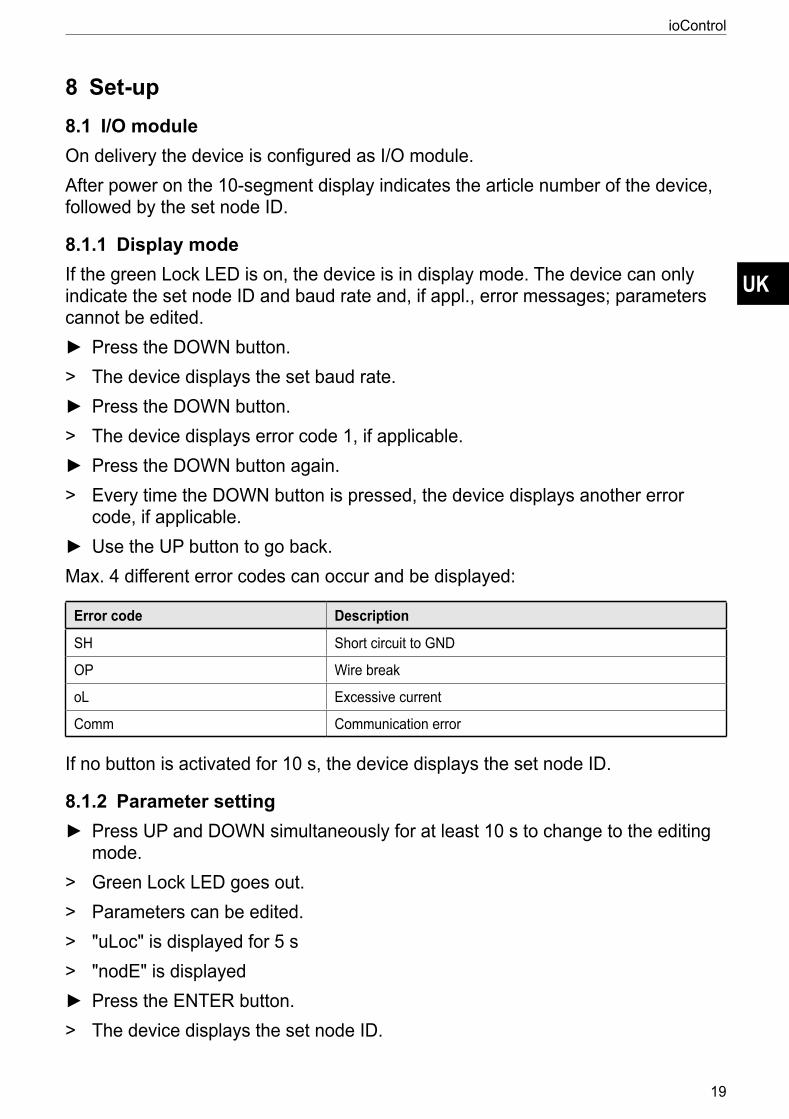
7.2 Status indication of the inputs/outputs (I/O LEDs, yellow)
I/O configuration(see attached object directory)
LED state Description
0 (not used) Off
1 (digital input BL) Off Input signal FALSE
On Input signal TRUE
2 (digital output BH) Off Output signal FALSE
On Output signal TRUE
3 (voltage input 10 V) Off
4 (PWM output) Off PWM value = 0‰
On PWM value > 0 ‰
5 (current-controlled output) Off Current value ≤ 20 mA
On Current value > 20 mA
6 (voltage input 32 V, ratiometric) Off
7 (current input 20 mA) Off
2 Hz Fault at the input
9 (voltage input 32 V) Off
10 (digital input BL) Off Input signal FALSE
On Input signal TRUE
11 (digital input BL, with diagnostics) Off Input signal FALSE
On Input signal TRUE
2 Hz Fault at the input
12 (digital input BH) Off Input signal FALSE
On Input signal TRUE
14 (frequency input) Off
2 Hz Fault at the input
15 (digital output BH, with diagnostics) Off Output signal FALSE
On Output signal TRUE
2 Hz Fault at the output
16 (digital output BH, with diagnostics, short-circuit proof and overload protected
Off Output signal FALSE
On Output signal TRUE
2 Hz Fault at the output
18 (resistor input) Off
2 Hz Fault at the input
20 (interval measurement) Off
2 Hz Fault at the input
UK
ioControl
19
8 Set-up8.1 I/O moduleOn delivery the device is configured as I/O moduleAfter power on the 10-segment display indicates the article number of the device, followed by the set node ID
8.1.1 Display modeIf the green Lock LED is on, the device is in display mode The device can only indicate the set node ID and baud rate and, if appl, error messages; parameters cannot be edited
Press the DOWN button > The device displays the set baud rate Press the DOWN button
> The device displays error code 1, if applicable Press the DOWN button again
> Every time the DOWN button is pressed, the device displays another error code, if applicable
Use the UP button to go backMax 4 different error codes can occur and be displayed:
Error code Description
SH Short circuit to GND
OP Wire break
oL Excessive current
Comm Communication error
If no button is activated for 10 s, the device displays the set node ID
8.1.2 Parameter setting Press UP and DOWN simultaneously for at least 10 s to change to the editing mode
> Green Lock LED goes out > Parameters can be edited > "uLoc" is displayed for 5 s > "nodE" is displayed Press the ENTER button
> The device displays the set node ID
ioControl
20
> The 1st digit to be edited flashes Use the UP and DOWN buttons to set the requested value Use the ENTER button to go to the next digit
> The 2nd digit to be edited flashes Use the UP and DOWN buttons to set the requested value Use the ENTER button to go to the next digit
> The 3rd digit to be edited flashes Use the UP and DOWN buttons to set the requested value Press the ENTER button
> The set node ID is confirmed > "nodE" is displayed Press the DOWN button
> "BAUD" is displayed Press the ENTER button
> The device displays the set baud rate Use the UP and DOWN buttons to set the requested value Press the ENTER button
> The set baud rate is confirmed
Changes of the parameters are only applied after a reset of the device
Exit the editing mode: Press UP and DOWN simultaneously for at least 10 s
> Green Lock LED on > parameters cannot be edited > "Loc" is displayed for 5 s, then the set node ID is displayed
If no button is activated for 30 s, the device automatically finishes the editing mode
8.1.3 List of parameters
Parameter Function Value range Default value
nodE Node ID of the device
1125 125
BAUD Baud rate 20, 50, 100, 125, 250, 500, 800, 1000 kBit/s 250 kBits/s
UK
ioControl
21
8.2 ControllerThe device can be configured as a controller The existing menu structure and the properties as I/O module will be lost
8.2.1 ProgrammingThe user can easily create the application software by means of the IEC 61131-3 compliant programming system CODESYS 23
The user is responsible for the safe function of the application programs which he created himself If necessary, he must additionally carry out an approval by corresponding supervisory and test organisations according to the national regulations
For notes on the setting of the CAN ID and the baud rate when used as CANopen device, refer to the system manual
8.3 Required documentationIn addition to the CODESYS V23 programming system, the following documents are required for programming and set-up of the device:
Programming manual CODESYS V23 (alternatively as online help)
System manual ioControl (alternatively as online help)
The manuals can be downloaded from the internet: wwwifmcom
8.4 Required hardwareIf used as mobile controller a CAN interface for connection to a PC or notebook is required to load the application program to the deviceExample:
CAN/RS232 USB interface CANfox (EC2112) adapter cable for CANfox (EC2113)
You can find more information about the available accessories at: wwwifmcom
ioControl
22
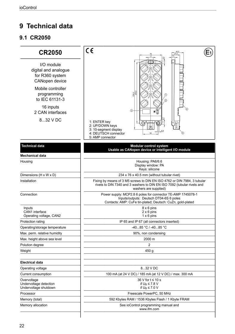
9 Technical data9.1 CR2050Control systems
ifm electronic gmbh • Friedrichstraße 1 • 45128 Essen We reserve the right to make technical alterations without prior notice! 04/12/2019CR2050 / page 1
CR2050
1: ENTER key2: UP/DOWN keys3: 10-segment display4: DEUTSCH connector5: AMP connector
Original Scale Drawing (MTD)P_MZ_e100_0092
EPS SourceProduct Scale DrawingFrame Size: 80 mm x 90 mm
30% 333,4%
1 2
4
6
8
3
5
7
205,
523
4,2
76
52
17
6,9
8,7
6,9
1
2
3
27,411
40,5
4
5
1 2
4
6
8
3
5
7
205,
523
4,2
76
52
17
6,9
8,7
6,9
1
2
3
27,411
40,5
4
5
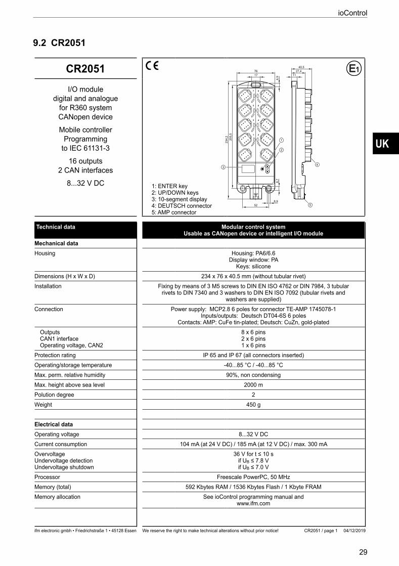
I/O moduledigital and analogue
for R360 systemCANopen device
Mobile controllerprogramming
to IEC 61131-3
16 inputs2 CAN interfaces
832 V DC
Technical data Modular control systemUsable as CANopen device or intelligent I/O module
Mechanical dataHousing Housing: PA6/66
Display window: PAKeys: silicone
Dimensions (H x W x D) 234 x 76 x 405 mm (without tubular rivet)Installation Fixing by means of 3 M5 screws to DIN EN ISO 4762 or DIN 7984, 3 tubular
rivets to DIN 7340 and 3 washers to DIN EN ISO 7092 (tubular rivets and washers are supplied)
Connection Power supply: MCP28 6 poles for connector TE-AMP 1745078-1Inputs/outputs: Deutsch DT04-6S 6 poles
Contacts: AMP: CuFe tin-plated; Deutsch: CuZn, gold-platedInputsCAN1 interfaceOperating voltage, CAN2
8 x 6 pins2 x 6 pins1 x 6 pins
Protection rating IP 65 and IP 67 (all connectors inserted)Operating/storage temperature -4085 °C / -4085 °CMax perm relative humidity 90%, non condensingMax height above sea level 2000 mPolution degree 2Weight 450 g
Electrical dataOperating voltage 832 V DCCurrent consumption 100 mA (at 24 V DC) / 185 mA (at 12 V DC) / max 300 mAOvervoltageUndervoltage detectionUndervoltage shutdown
36 V for t ≤ 10 sif UB ≤ 7.8 Vif UB ≤ 7.0 V
Processor Freescale PowerPC, 50 MHzMemory (total) 592 Kbytes RAM / 1536 Kbytes Flash / 1 Kbyte FRAMMemory allocation See ioControl programming manual and
wwwifmcom
UK
ioControl
23
ifm electronic gmbh • Friedrichstraße 1 • 45128 Essen We reserve the right to make technical alterations without prior notice! 04/12/2019CR2050 / page 2
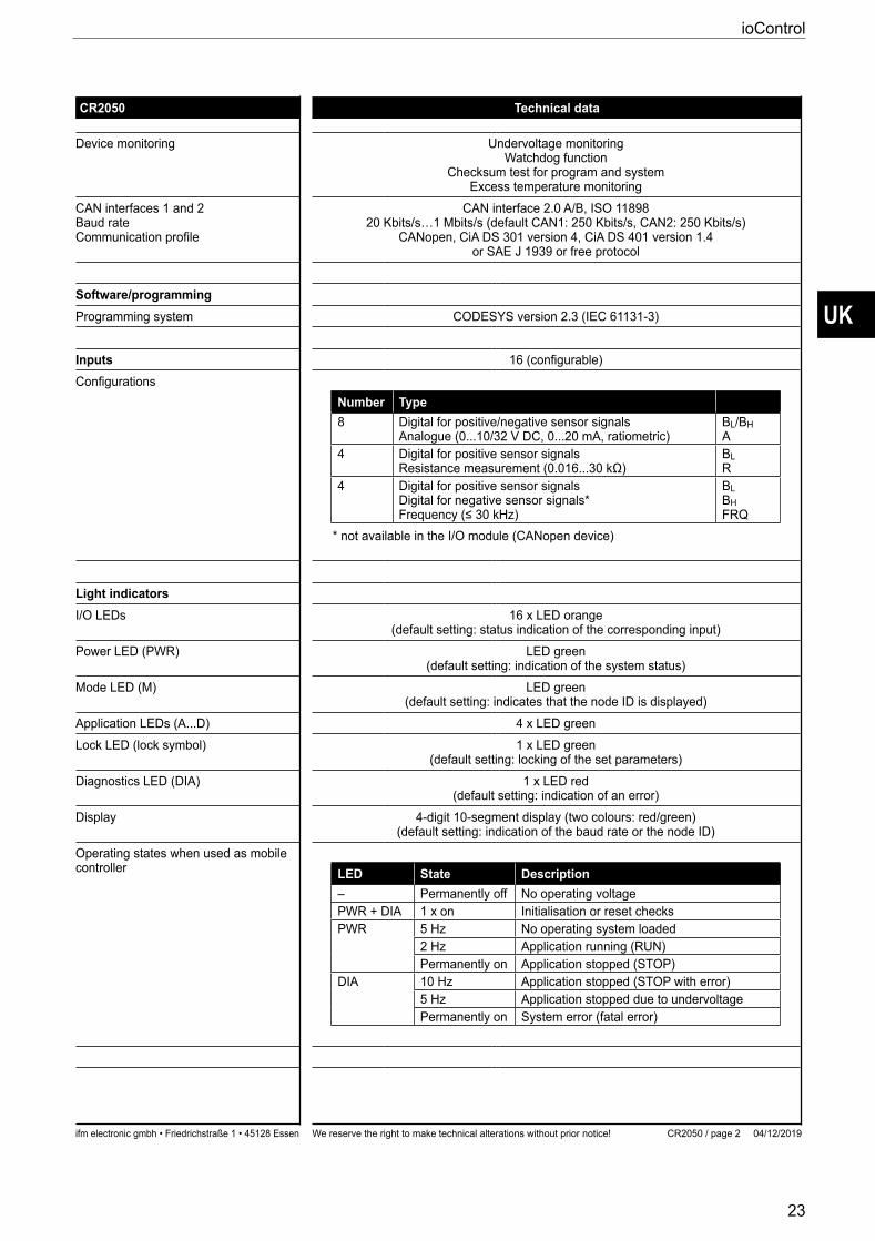
CR2050 Technical data
Control systems
Device monitoring Undervoltage monitoringWatchdog function
Checksum test for program and systemExcess temperature monitoring
CAN interfaces 1 and 2Baud rateCommunication profi le
CAN interface 20 A/B, ISO 1189820 Kbits/s…1 Mbits/s (default CAN1: 250 Kbits/s, CAN2: 250 Kbits/s)
CANopen, CiA DS 301 version 4, CiA DS 401 version 14or SAE J 1939 or free protocol
Software/programmingProgramming system CODESYS version 23 (IEC 61131-3)
Inputs 16 (confi gurable)Confi gurations
Number Type8 Digital for positive/negative sensor signals
Analogue (010/32 V DC, 020 mA, ratiometric)BL/BHA
4 Digital for positive sensor signalsResistance measurement (0.016...30 kΩ)
BLR
4 Digital for positive sensor signalsDigital for negative sensor signals*Frequency (≤ 30 kHz)
BLBHFRQ
* not available in the I/O module (CANopen device)
Light indicatorsI/O LEDs 16 x LED orange
(default setting: status indication of the corresponding input)Power LED (PWR) LED green
(default setting: indication of the system status)Mode LED (M) LED green
(default setting: indicates that the node ID is displayed)Application LEDs (AD) 4 x LED greenLock LED (lock symbol) 1 x LED green
(default setting: locking of the set parameters)Diagnostics LED (DIA) 1 x LED red
(default setting: indication of an error)Display 4-digit 10-segment display (two colours: red/green)
(default setting: indication of the baud rate or the node ID)Operating states when used as mobile controller LED State Description
– Permanently off No operating voltagePWR + DIA 1 x on Initialisation or reset checksPWR 5 Hz No operating system loaded
2 Hz Application running (RUN)Permanently on Application stopped (STOP)
DIA 10 Hz Application stopped (STOP with error)5 Hz Application stopped due to undervoltagePermanently on System error (fatal error)
ioControl
24
ifm electronic gmbh • Friedrichstraße 1 • 45128 Essen We reserve the right to make technical alterations without prior notice! 04/12/2019CR2050 / page 3
CR2050 Technical data
Control systems
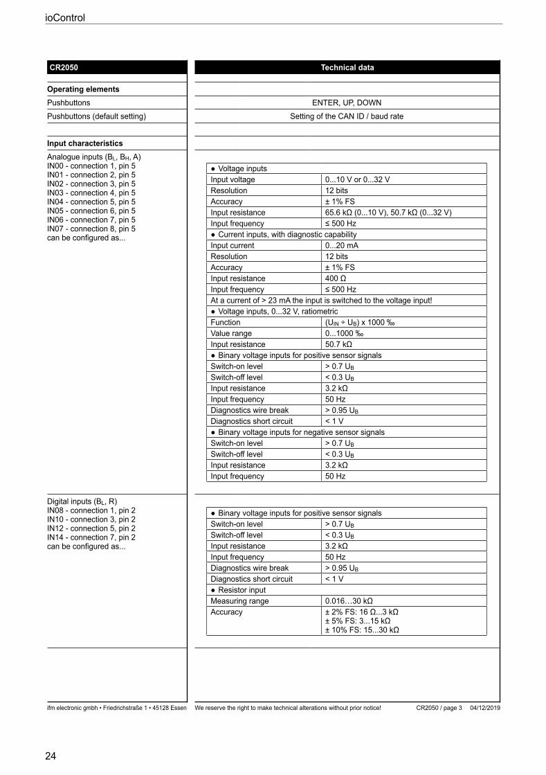
Operating elementsPushbuttons ENTER, UP, DOWNPushbuttons (default setting) Setting of the CAN ID / baud rate
Input characteristicsAnalogue inputs (BL, BH, A)IN00 - connection 1, pin 5IN01 - connection 2, pin 5IN02 - connection 3, pin 5IN03 - connection 4, pin 5IN04 - connection 5, pin 5IN05 - connection 6, pin 5IN06 - connection 7, pin 5IN07 - connection 8, pin 5can be confi gured as...
Voltage inputsInput voltage 010 V or 032 VResolution 12 bitsAccuracy ± 1% FSInput resistance 65.6 kΩ (0...10 V), 50.7 kΩ (0...32 V)Input frequency ≤ 500 Hz
Current inputs, with diagnostic capabilityInput current 020 mAResolution 12 bitsAccuracy ± 1% FSInput resistance 400 ΩInput frequency ≤ 500 HzAt a current of > 23 mA the input is switched to the voltage input!
Voltage inputs, 032 V, ratiometricFunction (UIN ÷ UB) x 1000 ‰Value range 01000 ‰Input resistance 50.7 kΩ
Binary voltage inputs for positive sensor signalsSwitch-on level > 07 UB
Switch-off level < 03 UB
Input resistance 3.2 kΩInput frequency 50 HzDiagnostics wire break > 095 UB
Diagnostics short circuit < 1 V Binary voltage inputs for negative sensor signals
Switch-on level > 07 UB
Switch-off level < 03 UB
Input resistance 3.2 kΩInput frequency 50 Hz
Digital inputs (BL, R)IN08 - connection 1, pin 2IN10 - connection 3, pin 2IN12 - connection 5, pin 2IN14 - connection 7, pin 2can be confi gured as...
Binary voltage inputs for positive sensor signalsSwitch-on level > 07 UB
Switch-off level < 03 UB
Input resistance 3.2 kΩInput frequency 50 HzDiagnostics wire break > 095 UB
Diagnostics short circuit < 1 V Resistor input
Measuring range 0.016…30 kΩAccuracy ± 2% FS: 16 Ω...3 kΩ
± 5% FS: 3...15 kΩ± 10% FS: 15...30 kΩ
UK
ioControl
25
ifm electronic gmbh • Friedrichstraße 1 • 45128 Essen We reserve the right to make technical alterations without prior notice! 04/12/2019CR2050 / page 4
CR2050 Technical data
Control systems
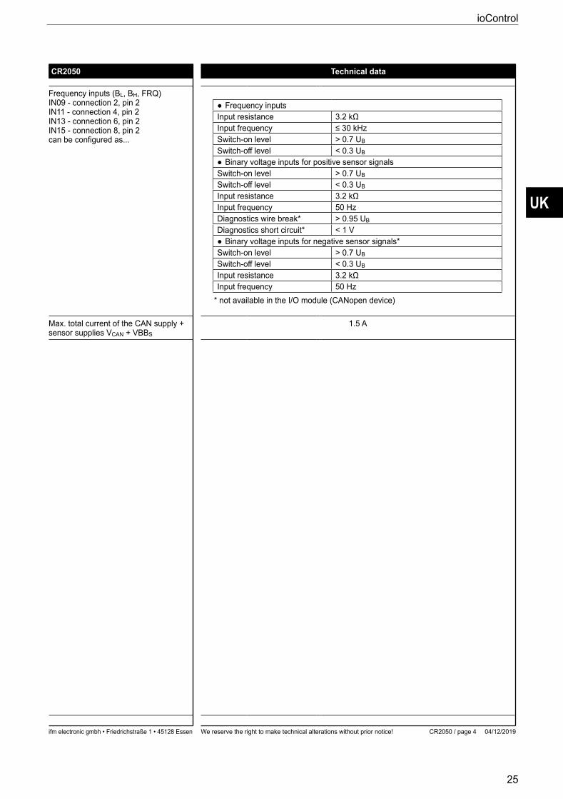
Frequency inputs (BL, BH, FRQ)IN09 - connection 2, pin 2IN11 - connection 4, pin 2IN13 - connection 6, pin 2IN15 - connection 8, pin 2can be confi gured as...
Frequency inputsInput resistance 3.2 kΩ Input frequency ≤ 30 kHzSwitch-on level > 07 UB
Switch-off level < 03 UB
Binary voltage inputs for positive sensor signalsSwitch-on level > 07 UB
Switch-off level < 03 UB
Input resistance 3.2 kΩInput frequency 50 HzDiagnostics wire break* > 095 UB
Diagnostics short circuit* < 1 V Binary voltage inputs for negative sensor signals*
Switch-on level > 07 UB
Switch-off level < 03 UB
Input resistance 3.2 kΩInput frequency 50 Hz
* not available in the I/O module (CANopen device)
Max total current of the CAN supply + sensor supplies VCAN + VBBS
15 A
ioControl
26
ifm electronic gmbh • Friedrichstraße 1 • 45128 Essen We reserve the right to make technical alterations without prior notice! 04/12/2019CR2050 / page 5
CR2050 Technical data
Control systems
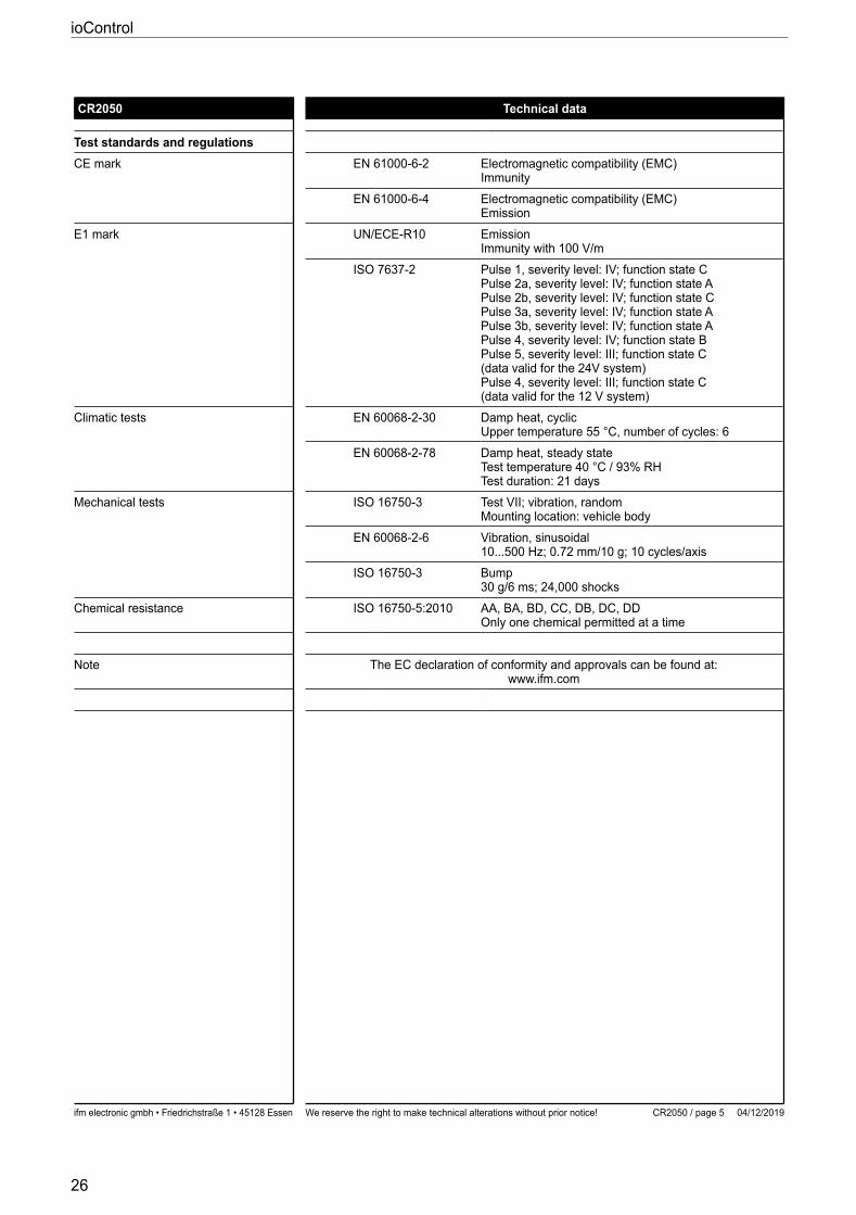
Test standards and regulationsCE mark EN 61000-6-2 Electromagnetic compatibility (EMC)
ImmunityEN 61000-6-4 Electromagnetic compatibility (EMC)
EmissionE1 mark UN/ECE-R10 Emission
Immunity with 100 V/mISO 7637-2 Pulse 1, severity level: IV; function state C
Pulse 2a, severity level: IV; function state APulse 2b, severity level: IV; function state CPulse 3a, severity level: IV; function state APulse 3b, severity level: IV; function state APulse 4, severity level: IV; function state BPulse 5, severity level: III; function state C(data valid for the 24V system)Pulse 4, severity level: III; function state C(data valid for the 12 V system)
Climatic tests EN 60068-2-30 Damp heat, cyclicUpper temperature 55 °C, number of cycles: 6
EN 60068-2-78 Damp heat, steady stateTest temperature 40 °C / 93% RHTest duration: 21 days
Mechanical tests ISO 16750-3 Test VII; vibration, randomMounting location: vehicle body
EN 60068-2-6 Vibration, sinusoidal10500 Hz; 072 mm/10 g; 10 cycles/axis
ISO 16750-3 Bump30 g/6 ms; 24,000 shocks
Chemical resistance ISO 16750-5:2010 AA, BA, BD, CC, DB, DC, DDOnly one chemical permitted at a time
Note The EC declaration of conformity and approvals can be found at:wwwifmcom
UK
ioControl
27
ifm electronic gmbh • Friedrichstraße 1 • 45128 Essen We reserve the right to make technical alterations without prior notice! 04/12/2019CR2050 / page 6
CR2050 Technical data
Control systems
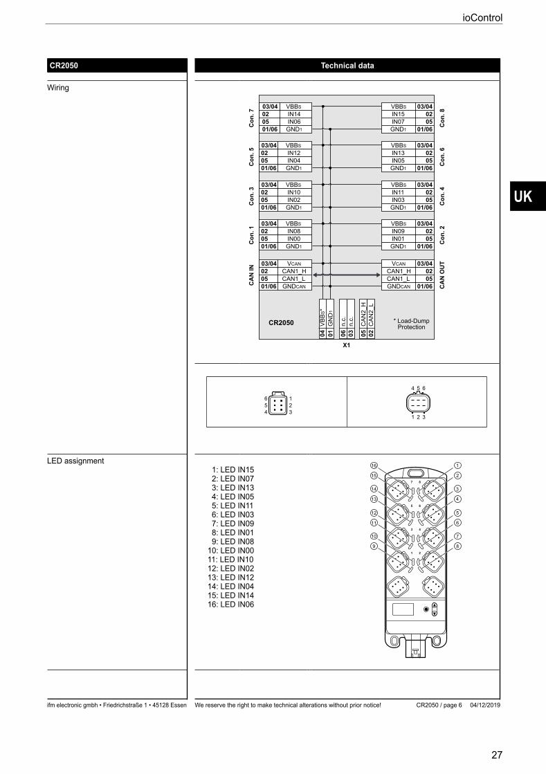
Wiring
Con
. 7
Con
. 8
CR2050 * Load-DumpProtection
03/04 VBBS
05IN14IN06
02
01/06 GND1
03/04
0502
01/06
VBBS
IN15IN07GND1
Con
. 5
Con
. 6
03/04 VBBS
05IN12IN04
02
01/06 GND1
03/04
0502
01/06
VBBS
IN13IN05GND1
Con
. 3
Con
. 4
03/04 VBBS
05IN10IN02
02
01/06 GND1
03/04
0502
01/06
VBBS
IN11IN03GND1
Con
. 1
Con
. 2
03/04 VBBS
05IN08IN00
02
01/06 GND1
03/04
0502
01/06
VBBS
IN09IN01
CA
N IN
CA
N O
UT03/04 VCAN
05CAN1_HCAN1_L
02
01/06 GNDCAN
VB
BS*
06
GN
D1
n.c.
0104
03/04
0502
01/06
GND1
VCAN
CAN1_HCAN1_LGNDCAN
03n.
c.
05C
AN
2_H
02C
AN
2_L
X1
Original Scale Drawing (MTD)PIN_0193
456 1
23
456 1
23
EPS SourceFrame Size: 15 mm x 15 mm
50% 200%
Original Scale Drawing (MTD)
EPS SourceFrame Size: 15 mm x 15 mm
PIN_0196
4 5 6
1 2 3
4 5 6
1 2 3
LED assignment 1: LED IN15 2: LED IN07 3: LED IN13 4: LED IN05 5: LED IN11 6: LED IN03 7: LED IN09 8: LED IN01 9: LED IN0810: LED IN0011: LED IN1012: LED IN0213: LED IN1214: LED IN0415: LED IN1416: LED IN06
Original Scale Drawing (MTD)P_MZ_e100_0092
EPS SourceProduct Scale DrawingFrame Size: 80 mm x 90 mm
30% 333,4%
1
2
3
4
5
6
7
8
16
15
14
13
12
11
10
9
1 2
4
6
8
3
5
7
205,
523
4,2
76
52
17
6,9
8,7
6,9
1
2
3
27,411
40,5
4
5
1 2
4
6
8
3
5
7
ioControl
28
ifm electronic gmbh • Friedrichstraße 1 • 45128 Essen We reserve the right to make technical alterations without prior notice! 04/12/2019CR2050 / page 7
CR2050 Technical data
Control systems
Abbreviations ABHBLFRQRVBBS VCAN
AnalogueBinary high sideBinary low sideFrequency/pulse inputResistor inputSupply sensors/moduleSupply CAN connector
UK
ioControl
29
9.2 CR2051Control systems
ifm electronic gmbh • Friedrichstraße 1 • 45128 Essen We reserve the right to make technical alterations without prior notice! 04/12/2019CR2051 / page 1
CR2051
1: ENTER key2: UP/DOWN keys3: 10-segment display4: DEUTSCH connector5: AMP connector
Original Scale Drawing (MTD)P_MZ_e100_0092
EPS SourceProduct Scale DrawingFrame Size: 80 mm x 90 mm
30% 333,4%
1 2
4
6
8
3
5
7
205,
523
4,2
76
52
17
6,9
8,7
6,9
1
2
3
27,411
40,5
4
5
1 2
4
6
8
3
5
7
205,
523
4,2
76
52
17
6,9
8,7
6,9
1
2
3
27,411
40,5
4
5
I/O moduledigital and analogue
for R360 systemCANopen device
Mobile controllerProgramming
to IEC 61131-3
16 outputs2 CAN interfaces
832 V DC
Technical data Modular control systemUsable as CANopen device or intelligent I/O module
Mechanical dataHousing Housing: PA6/66
Display window: PAKeys: silicone
Dimensions (H x W x D) 234 x 76 x 405 mm (without tubular rivet)Installation Fixing by means of 3 M5 screws to DIN EN ISO 4762 or DIN 7984, 3 tubular
rivets to DIN 7340 and 3 washers to DIN EN ISO 7092 (tubular rivets and washers are supplied)
Connection Power supply: MCP28 6 poles for connector TE-AMP 1745078-1Inputs/outputs: Deutsch DT04-6S 6 poles
Contacts: AMP: CuFe tin-plated; Deutsch: CuZn, gold-platedOutputsCAN1 interfaceOperating voltage, CAN2
8 x 6 pins2 x 6 pins1 x 6 pins
Protection rating IP 65 and IP 67 (all connectors inserted)Operating/storage temperature -4085 °C / -4085 °CMax perm relative humidity 90%, non condensingMax height above sea level 2000 mPolution degree 2Weight 450 g
Electrical dataOperating voltage 832 V DCCurrent consumption 104 mA (at 24 V DC) / 185 mA (at 12 V DC) / max 300 mAOvervoltageUndervoltage detectionUndervoltage shutdown
36 V for t ≤ 10 sif UB ≤ 7.8 Vif UB ≤ 7.0 V
Processor Freescale PowerPC, 50 MHzMemory (total) 592 Kbytes RAM / 1536 Kbytes Flash / 1 Kbyte FRAMMemory allocation See ioControl programming manual and
wwwifmcom
ioControl
30
ifm electronic gmbh • Friedrichstraße 1 • 45128 Essen We reserve the right to make technical alterations without prior notice! 04/12/2019CR2051 / page 2
CR2051 Technical data
Control systems
Device monitoring Undervoltage monitoringWatchdog function
Checksum test for program and systemExcess temperature monitoring
CAN interfaces 1 and 2Baud rateCommunication profi le
CAN interface 20 A/B, ISO 1189820 Kbits/s…1 Mbits/s (default CAN1: 250 Kbits/s, CAN2: 250 Kbits/s)
CANopen, CiA DS 301 version 4, CiA DS 401 version 14or SAE J 1939 or free protocol
Software/programmingProgramming system CODESYS version 23 (IEC 61131-3)
Outputs 16 (confi gurable)Confi gurations
Number Type4 Positive-switching (high side), 4 A, diagnostics
PWM output (20…250 Hz), 4A, diagnosticsCurrent-controlled 002…4 A
BHPWMPWMI
4 Positive-switching (high side), 25 A, diagnosticsPWM output (20…250 Hz), 25A, diagnosticsCurrent-controlled 002…25 A
BHPWMPWMI
4 Positive-switching (high side), 4 A, diagnosticsPWM output (20…250 Hz), 4A
BHPWM
4 Positive-switching (high side), 25 A, diagnosticsPWM output (20…250 Hz), 25A
BHPWM
Light indicatorsI/O LEDs 16 x LED orange
(default setting: status indication of the corresponding output)Power LED (PWR) LED green
(default setting: indication of the system status)Mode LED (M) LED green
(default setting: indicates that the node ID is displayed)Application LEDs (AD) 4 x LED greenLock LED (lock symbol) 1 x LED green
(default setting: locking of the set parameters)Diagnostics LED (DIA) 1 x LED red
(default setting: indication of an error)Display 4-digit 10-segment display (two colours: red/green)
(default setting: indication of the baud rate or the node ID)Operating states when used as mobile controller LED State Description
– Permanently off No operating voltagePWR + DIA 1 x on Initialisation or reset checksPWR 5 Hz No operating system loaded
2 Hz Application running (RUN)Permanently on Application stopped (STOP)
DIA 10 Hz Application stopped (STOP with error)5 Hz Application stopped due to undervoltagePermanently on System error (fatal error)
UK
ioControl
31
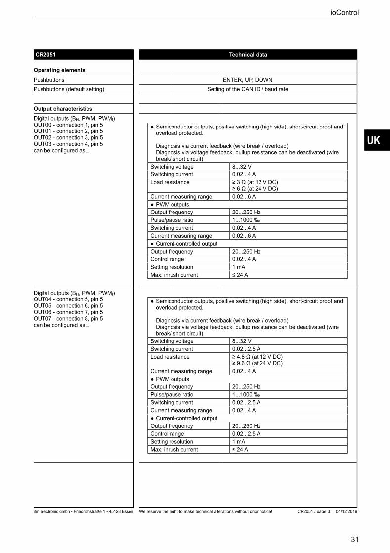
ifm electronic gmbh • Friedrichstraße 1 • 45128 Essen We reserve the right to make technical alterations without prior notice! 04/12/2019CR2051 / page 3
CR2051 Technical data
Control systems
Operating elementsPushbuttons ENTER, UP, DOWNPushbuttons (default setting) Setting of the CAN ID / baud rate
Output characteristicsDigital outputs (BH, PWM, PWMI)OUT00 - connection 1, pin 5OUT01 - connection 2, pin 5OUT02 - connection 3, pin 5OUT03 - connection 4, pin 5can be confi gured as...
Semiconductor outputs, positive switching (high side), short-circuit proof and overload protected
Diagnosis via current feedback (wire break / overload)Diagnosis via voltage feedback, pullup resistance can be deactivated (wire break/ short circuit)
Switching voltage 832 VSwitching current 0024 ALoad resistance ≥ 3 Ω (at 12 V DC)
≥ 6 Ω (at 24 V DC)Current measuring range 0026 A
PWM outputsOutput frequency 20250 HzPulse/pause ratio 11000 ‰Switching current 0024 ACurrent measuring range 0026 A
Current-controlled outputOutput frequency 20250 HzControl range 0024 ASetting resolution 1 mAMax inrush current ≤ 24 A
Digital outputs (BH, PWM, PWMI)OUT04 - connection 5, pin 5OUT05 - connection 6, pin 5OUT06 - connection 7, pin 5OUT07 - connection 8, pin 5can be confi gured as...
Semiconductor outputs, positive switching (high side), short-circuit proof and overload protected
Diagnosis via current feedback (wire break / overload)Diagnosis via voltage feedback, pullup resistance can be deactivated (wire break/ short circuit)
Switching voltage 832 VSwitching current 00225 ALoad resistance ≥ 4.8 Ω (at 12 V DC)
≥ 9.6 Ω (at 24 V DC)Current measuring range 0024 A
PWM outputsOutput frequency 20250 HzPulse/pause ratio 11000 ‰Switching current 00225 ACurrent measuring range 0024 A
Current-controlled outputOutput frequency 20250 HzControl range 00225 ASetting resolution 1 mAMax inrush current ≤ 24 A
ioControl
32
ifm electronic gmbh • Friedrichstraße 1 • 45128 Essen We reserve the right to make technical alterations without prior notice! 04/12/2019CR2051 / page 4
CR2051 Technical data
Control systems
Digital outputs (BH, PWM)OUT08 - connection 1, pin 2OUT09 - connection 2, pin 2OUT10 - connection 3, pin 2OUT11 - connection 4, pin 2can be confi gured as...
Semiconductor outputs, positive switching (high side), short-circuit proof and overload protected
Diagnosis via voltage feedback, pullup resistance can be deactivated (wire break/ short circuit)
Switching voltage 832 VSwitching current 00225 A
PWM outputsOutput frequency 20250 HzPulse/pause ratio 11000 ‰Switching current 00225 AMax inrush current ≤ 24 A
Digital outputs (BH, PWM)OUT12 - connection 5, pin 2OUT13 - connection 6, pin 2OUT14 - connection 7, pin 2OUT15 - connection 8, pin 2can be confi gured as...
Semiconductor outputs, positive switching (high side), short-circuit proof and overload protected
Diagnosis via voltage feedback, pullup resistance can be deactivated (wire break/ short circuit)
Switching voltage 832 VSwitching current 0024 A
PWM outputsOutput frequency 20250 HzPulse/pause ratio 11000 ‰Switching current 0024 AMax inrush current ≤ 24 A
Free wheel diodes Free wheel diodes for the deactivation of inductive loads are integratedOverload protection(valid for all outputs)
≤ 5 minutes (at 100% overload)
Short-circuit strength(valid for all inputs and outputs)
≤ 5 minutes
Max total current of the CAN supply VCAN
15 A
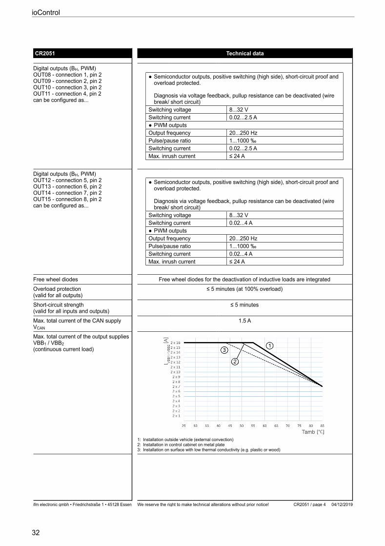
Max total current of the output supplies VBB1 / VBB2(continuous current load)
1: Installation outside vehicle (external convection)2: Installation in control cabinet on metal plate3: Installation on surface with low thermal conductivity (eg plastic or wood)
UK
ioControl
33
ifm electronic gmbh • Friedrichstraße 1 • 45128 Essen We reserve the right to make technical alterations without prior notice! 04/12/2019CR2051 / page 5
CR2051 Technical data
Control systems
Test standards and regulationsCE mark EN 61000-6-2 Electromagnetic compatibility (EMC)
ImmunityEN 61000-6-4 Electromagnetic compatibility (EMC)
EmissionE1 mark UN/ECE-R10 Emission
Immunity with 100 V/mISO 7637-2 Pulse 1, severity level: IV; function state C
Pulse 2a, severity level: IV; function state APulse 2b, severity level: IV; function state CPulse 3a, severity level: IV; function state APulse 3b, severity level: IV; function state APulse 4, severity level: IV; function state BPulse 5, severity level: III; function state C(data valid for the 24V system)Pulse 4, severity level: III; function state C(data valid for the 12 V system)
Climatic tests EN 60068-2-30 Damp heat, cyclicUpper temperature 55 °C, number of cycles: 6
EN 60068-2-78 Damp heat, steady stateTest temperature 40 °C / 93% RHTest duration: 21 days
Mechanical tests ISO 16750-3 Test VII; vibration, randomMounting location: vehicle body
EN 60068-2-6 Vibration, sinusoidal10500 Hz; 072 mm/10 g; 10 cycles/axis
ISO 16750-3 Bump30 g/6 ms; 24,000 shocks
Chemical resistance ISO 16750-5:2010 AA, BA, BD, CC, DB, DC, DDOnly one chemical permitted at a time
Note The EC declaration of conformity and approvals can be found at:wwwifmcom
ioControl
34
ifm electronic gmbh • Friedrichstraße 1 • 45128 Essen We reserve the right to make technical alterations without prior notice! 04/12/2019CR2051 / page 6
CR2051 Technical data
Control systems
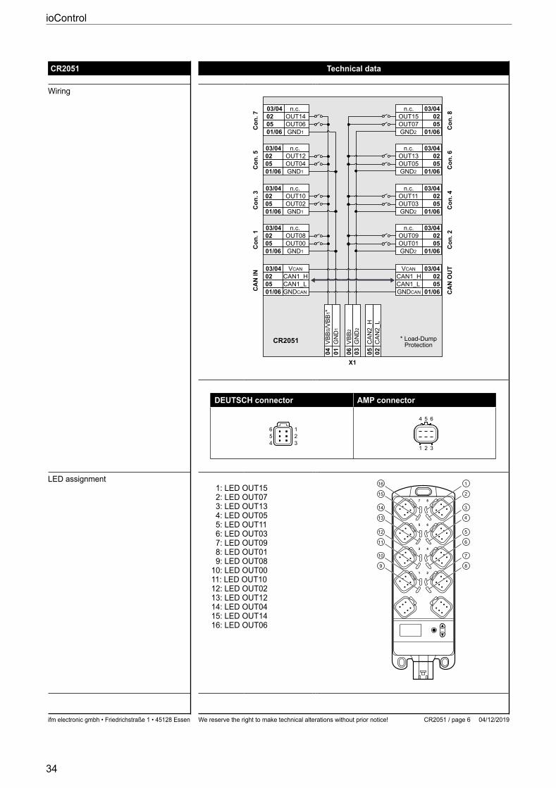
Wiring
Con
. 7
Con
. 8
CR2051 * Load-DumpProtection
03/04 n.c.
05OUT14OUT06
02
01/06 GND1
03/04
0502
01/06
n.c.OUT15OUT07GND2
Con
. 5
Con
. 6
03/04 n.c.
05OUT12OUT04
02
01/06 GND1
03/04
0502
01/06
n.c.OUT13OUT05GND2
Con
. 3
Con
. 4
03/04 n.c.
05OUT10OUT02
02
01/06 GND1
03/04
0502
01/06
n.c.OUT11OUT03GND2
Con
. 1
Con
. 2
03/04 n.c.
05OUT08OUT00
02
01/06 GND1
03/04
0502
01/06
n.c.OUT09OUT01
CA
N IN
CA
N O
UT03/04 VCAN
05CAN1_HCAN1_L
02
01/06 GNDCAN
VB
BS/V
BB
1 *
06
GN
D1
VB
B2
0104
03/04
0502
01/06
GND2
VCAN
CAN1_HCAN1_LGNDCAN
03G
ND
2
05C
AN
2_H
02C
AN
2_L
X1
DEUTSCH connector AMP connector
Original Scale Drawing (MTD)PIN_0193
456 1
23
456 1
23
EPS SourceFrame Size: 15 mm x 15 mm
50% 200%
Original Scale Drawing (MTD)
EPS SourceFrame Size: 15 mm x 15 mm
PIN_0196
4 5 6
1 2 3
4 5 6
1 2 3
LED assignment 1: LED OUT15 2: LED OUT07 3: LED OUT13 4: LED OUT05 5: LED OUT11 6: LED OUT03 7: LED OUT09 8: LED OUT01 9: LED OUT0810: LED OUT0011: LED OUT1012: LED OUT0213: LED OUT1214: LED OUT0415: LED OUT1416: LED OUT06
Original Scale Drawing (MTD)P_MZ_e100_0092
EPS SourceProduct Scale DrawingFrame Size: 80 mm x 90 mm
30% 333,4%
1
2
3
4
5
6
7
8
16
15
14
13
12
11
10
9
1 2
4
6
8
3
5
7
205,
523
4,2
76
52
17
6,9
8,7
6,9
1
2
3
27,411
40,5
4
5
1 2
4
6
8
3
5
7

UK
ioControl
35
ifm electronic gmbh • Friedrichstraße 1 • 45128 Essen We reserve the right to make technical alterations without prior notice! 04/12/2019CR2051 / page 7
CR2051 Technical data
Control systems
Abbreviations BHBLPWMPWMIVBBS VBB1VBB2VCAN
Binary high sideBinary low sidePulse width modulationPulse width modulation, current-controlledSupply sensors/moduleSupply OUT00, OUT02, OUT04, OUT06, OUT08, OUT10, OUT12, OUT14Supply OUT01, OUT03, OUT05, OUT07, OUT09, OUT11, OUT13, OUT15Supply CAN connector
ioControl
36
9.3 CR2052Control systems
ifm electronic gmbh • Friedrichstraße 1 • 45128 Essen We reserve the right to make technical alterations without prior notice! 04/12/2019CR2052 / page 1
CR2052
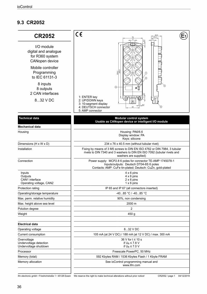
1: ENTER key2: UP/DOWN keys3: 10-segment display4: DEUTSCH connector5: AMP connector
Original Scale Drawing (MTD)P_MZ_e100_0092
EPS SourceProduct Scale DrawingFrame Size: 80 mm x 90 mm
30% 333,4%
1 2
4
6
8
3
5
7
205,
523
4,2
76
52
17
6,9
8,7
6,9
1
2
3
27,411
40,5
4
5
1 2
4
6
8
3
5
7
205,
523
4,2
76
52
17
6,9
8,7
6,9
1
2
3
27,411
40,5
4
5
I/O moduledigital and analogue
for R360 systemCANopen device
Mobile controllerProgramming
to IEC 61131-3
8 inputs8 outputs
2 CAN interfaces
832 V DC
Technical data Modular control systemUsable as CANopen device or intelligent I/O module
Mechanical dataHousing Housing: PA6/66
Display window: PAKeys: silicone
Dimensions (H x W x D) 234 x 76 x 405 mm (without tubular rivet)Installation Fixing by means of 3 M5 screws to DIN EN ISO 4762 or DIN 7984, 3 tubular
rivets to DIN 7340 and 3 washers to DIN EN ISO 7092 (tubular rivets and washers are supplied)
Connection Power supply: MCP28 6 poles for connector TE-AMP 1745078-1Inputs/outputs: Deutsch DT04-6S 6 poles
Contacts: AMP: CuFe tin-plated; Deutsch: CuZn, gold-platedInputsOutputsCAN1 interfaceOperating voltage, CAN2
4 x 6 pins4 x 6 pins2 x 6 pins1 x 6 pins
Protection rating IP 65 and IP 67 (all connectors inserted)Operating/storage temperature -4085 °C / -4085 °CMax perm relative humidity 90%, non condensingMax height above sea level 2000 mPolution degree 2Weight 450 g
Electrical dataOperating voltage 832 V DCCurrent consumption 105 mA (at 24 V DC) / 188 mA (at 12 V DC) / max 300 mAOvervoltageUndervoltage detectionUndervoltage shutdown
36 V for t ≤ 10 sif UB ≤ 7.8 Vif UB ≤ 7.0 V
Processor Freescale PowerPC, 50 MHzMemory (total) 592 Kbytes RAM / 1536 Kbytes Flash / 1 Kbyte FRAMMemory allocation See ioControl programming manual and
wwwifmcom
UK
ioControl
37
ifm electronic gmbh • Friedrichstraße 1 • 45128 Essen We reserve the right to make technical alterations without prior notice! 04/12/2019CR2052 / page 2
CR2052 Technical data
Control systems
Device monitoring Undervoltage monitoringWatchdog function
Checksum test for program and systemExcess temperature monitoring
CAN interfaces 1 and 2Baud rateCommunication profi le
CAN interface 20 A/B, ISO 1189820 Kbits/s…1 Mbits/s (default CAN1: 250 Kbits/s, CAN2: 250 Kbits/s)
CANopen, CiA DS 301 version 4, CiA DS 401 version 14or SAE J 1939 or free protocol
Software/programmingProgramming system CODESYS version 23 (IEC 61131-3)
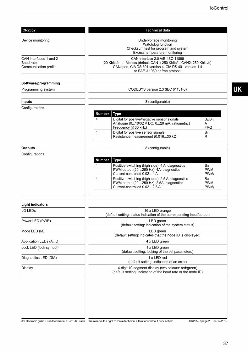
Inputs 8 (confi gurable)Confi gurations
Number Type4 Digital for positive/negative sensor signals
Analogue (010/32 V DC, 020 mA, ratiometric)Frequency (≤ 30 kHz)
BL/BHAFRQ
4 Digital for positive sensor signalsResistance measurement (0.016...30 kΩ)
BLR
Outputs 8 (confi gurable)Confi gurations
Number Type4 Positive-switching (high side), 4 A, diagnostics
PWM output (20…250 Hz), 4A, diagnosticsCurrent-controlled 002…4 A
BHPWMPWMI
4 Positive-switching (high side), 25 A, diagnosticsPWM output (20…250 Hz), 25A, diagnosticsCurrent-controlled 002…25 A
BHPWMPWMI
Light indicatorsI/O LEDs 16 x LED orange
(default setting: status indication of the corresponding input/output)Power LED (PWR) LED green
(default setting: indication of the system status)Mode LED (M) LED green
(default setting: indicates that the node ID is displayed)Application LEDs (AD) 4 x LED greenLock LED (lock symbol) 1 x LED green
(default setting: locking of the set parameters)Diagnostics LED (DIA) 1 x LED red
(default setting: indication of an error)Display 4-digit 10-segment display (two colours: red/green)
(default setting: indication of the baud rate or the node ID)
ioControl
38
ifm electronic gmbh • Friedrichstraße 1 • 45128 Essen We reserve the right to make technical alterations without prior notice! 04/12/2019CR2052 / page 3
CR2052 Technical data
Control systems
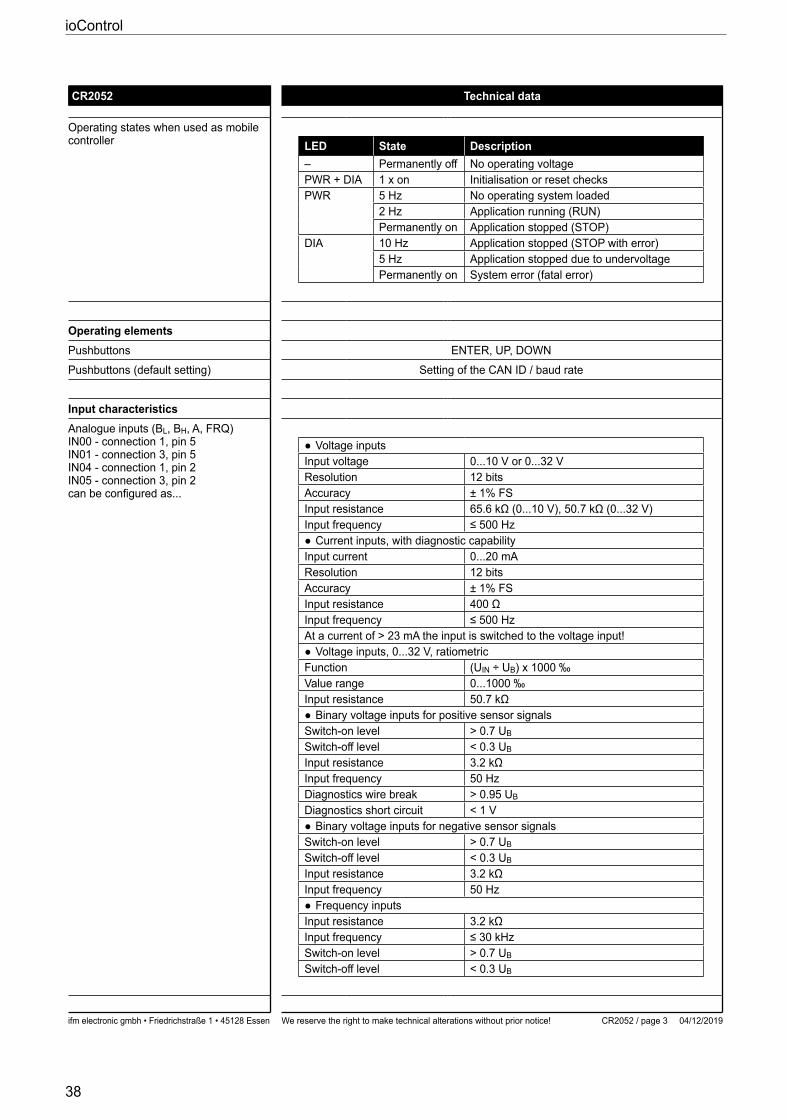
Operating states when used as mobile controller LED State Description
– Permanently off No operating voltagePWR + DIA 1 x on Initialisation or reset checksPWR 5 Hz No operating system loaded
2 Hz Application running (RUN)Permanently on Application stopped (STOP)
DIA 10 Hz Application stopped (STOP with error)5 Hz Application stopped due to undervoltagePermanently on System error (fatal error)
Operating elementsPushbuttons ENTER, UP, DOWNPushbuttons (default setting) Setting of the CAN ID / baud rate
Input characteristicsAnalogue inputs (BL, BH, A, FRQ)IN00 - connection 1, pin 5IN01 - connection 3, pin 5IN04 - connection 1, pin 2IN05 - connection 3, pin 2can be confi gured as...
Voltage inputsInput voltage 010 V or 032 VResolution 12 bitsAccuracy ± 1% FSInput resistance 65.6 kΩ (0...10 V), 50.7 kΩ (0...32 V)Input frequency ≤ 500 Hz
Current inputs, with diagnostic capabilityInput current 020 mAResolution 12 bitsAccuracy ± 1% FSInput resistance 400 ΩInput frequency ≤ 500 HzAt a current of > 23 mA the input is switched to the voltage input!
Voltage inputs, 032 V, ratiometricFunction (UIN ÷ UB) x 1000 ‰Value range 01000 ‰Input resistance 50.7 kΩ
Binary voltage inputs for positive sensor signalsSwitch-on level > 07 UB
Switch-off level < 03 UB
Input resistance 3.2 kΩInput frequency 50 HzDiagnostics wire break > 095 UB
Diagnostics short circuit < 1 V Binary voltage inputs for negative sensor signals
Switch-on level > 07 UB
Switch-off level < 03 UB
Input resistance 3.2 kΩInput frequency 50 Hz
Frequency inputsInput resistance 3.2 kΩ Input frequency ≤ 30 kHzSwitch-on level > 07 UB
Switch-off level < 03 UB
UK
ioControl
39
ifm electronic gmbh • Friedrichstraße 1 • 45128 Essen We reserve the right to make technical alterations without prior notice! 04/12/2019CR2052 / page 4
CR2052 Technical data
Control systems
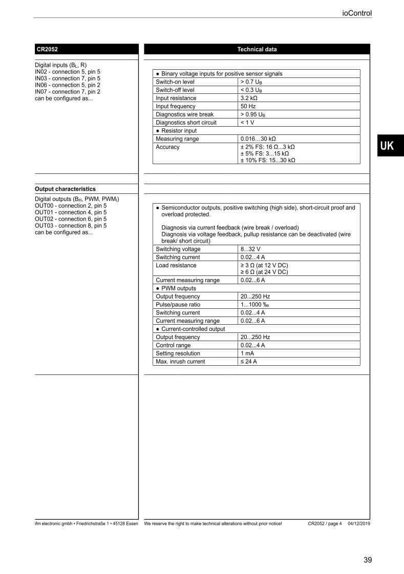
Digital inputs (BL, R)IN02 - connection 5, pin 5IN03 - connection 7, pin 5IN06 - connection 5, pin 2IN07 - connection 7, pin 2can be confi gured as...
Binary voltage inputs for positive sensor signalsSwitch-on level > 07 UB
Switch-off level < 03 UB
Input resistance 3.2 kΩInput frequency 50 HzDiagnostics wire break > 095 UB
Diagnostics short circuit < 1 V Resistor input
Measuring range 0.016…30 kΩAccuracy ± 2% FS: 16 Ω...3 kΩ
± 5% FS: 3...15 kΩ± 10% FS: 15...30 kΩ
Output characteristicsDigital outputs (BH, PWM, PWMI)OUT00 - connection 2, pin 5OUT01 - connection 4, pin 5OUT02 - connection 6, pin 5OUT03 - connection 8, pin 5can be confi gured as...
Semiconductor outputs, positive switching (high side), short-circuit proof and overload protected
Diagnosis via current feedback (wire break / overload)Diagnosis via voltage feedback, pullup resistance can be deactivated (wire break/ short circuit)
Switching voltage 832 VSwitching current 0024 ALoad resistance ≥ 3 Ω (at 12 V DC)
≥ 6 Ω (at 24 V DC)Current measuring range 0026 A
PWM outputsOutput frequency 20250 HzPulse/pause ratio 11000 ‰Switching current 0024 ACurrent measuring range 0026 A
Current-controlled outputOutput frequency 20250 HzControl range 0024 ASetting resolution 1 mAMax inrush current ≤ 24 A
ioControl
40
ifm electronic gmbh • Friedrichstraße 1 • 45128 Essen We reserve the right to make technical alterations without prior notice! 04/12/2019CR2052 / page 5
CR2052 Technical data
Control systems
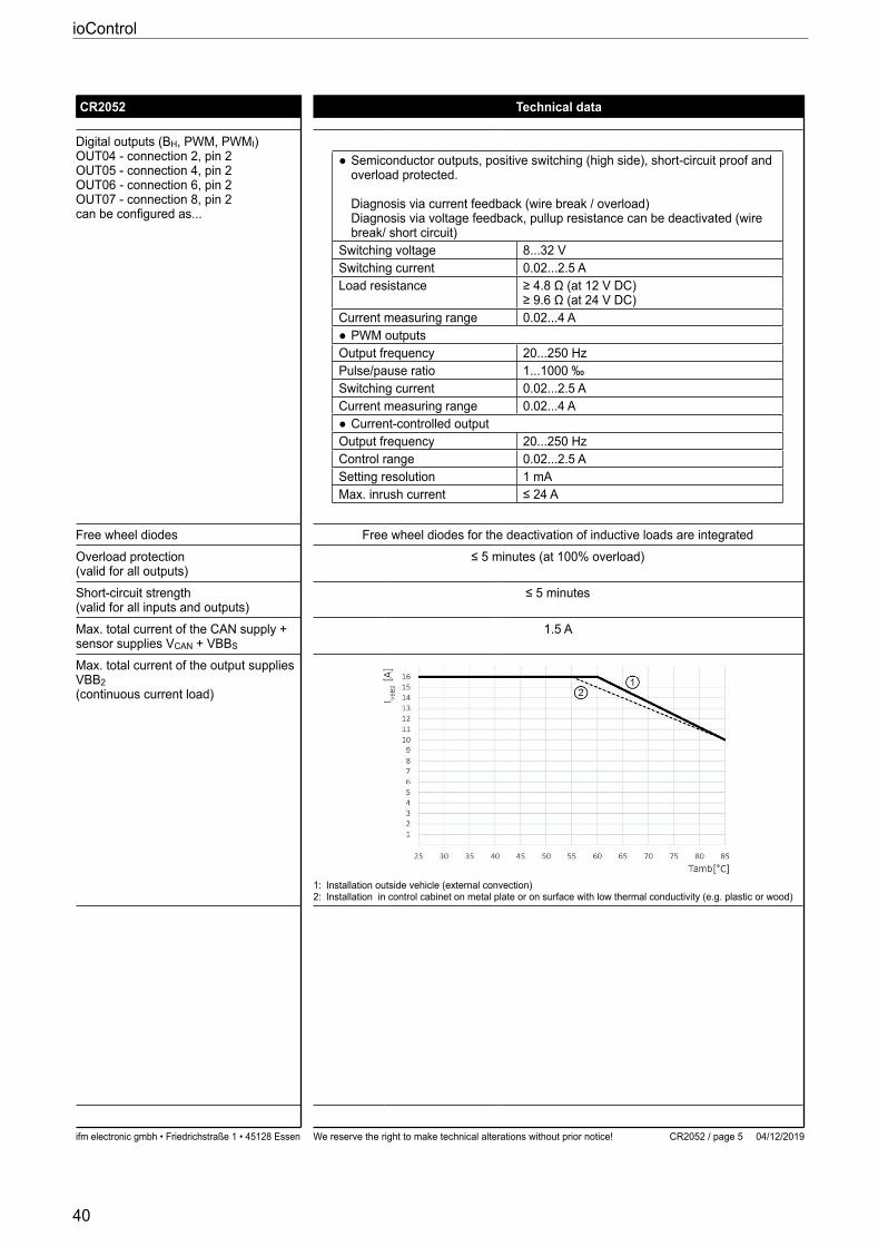
Digital outputs (BH, PWM, PWMI)OUT04 - connection 2, pin 2OUT05 - connection 4, pin 2OUT06 - connection 6, pin 2OUT07 - connection 8, pin 2can be confi gured as...
Semiconductor outputs, positive switching (high side), short-circuit proof and overload protected
Diagnosis via current feedback (wire break / overload)Diagnosis via voltage feedback, pullup resistance can be deactivated (wire break/ short circuit)
Switching voltage 832 VSwitching current 00225 ALoad resistance ≥ 4.8 Ω (at 12 V DC)
≥ 9.6 Ω (at 24 V DC)Current measuring range 0024 A
PWM outputsOutput frequency 20250 HzPulse/pause ratio 11000 ‰Switching current 00225 ACurrent measuring range 0024 A
Current-controlled outputOutput frequency 20250 HzControl range 00225 ASetting resolution 1 mAMax inrush current ≤ 24 A
Free wheel diodes Free wheel diodes for the deactivation of inductive loads are integratedOverload protection(valid for all outputs)
≤ 5 minutes (at 100% overload)
Short-circuit strength(valid for all inputs and outputs)
≤ 5 minutes
Max total current of the CAN supply + sensor supplies VCAN + VBBS
15 A
Max total current of the output supplies VBB2(continuous current load)
1: Installation outside vehicle (external convection)2: Installation in control cabinet on metal plate or on surface with low thermal conductivity (eg plastic or wood)
UK
ioControl
41
ifm electronic gmbh • Friedrichstraße 1 • 45128 Essen We reserve the right to make technical alterations without prior notice! 04/12/2019CR2052 / page 6
CR2052 Technical data
Control systems
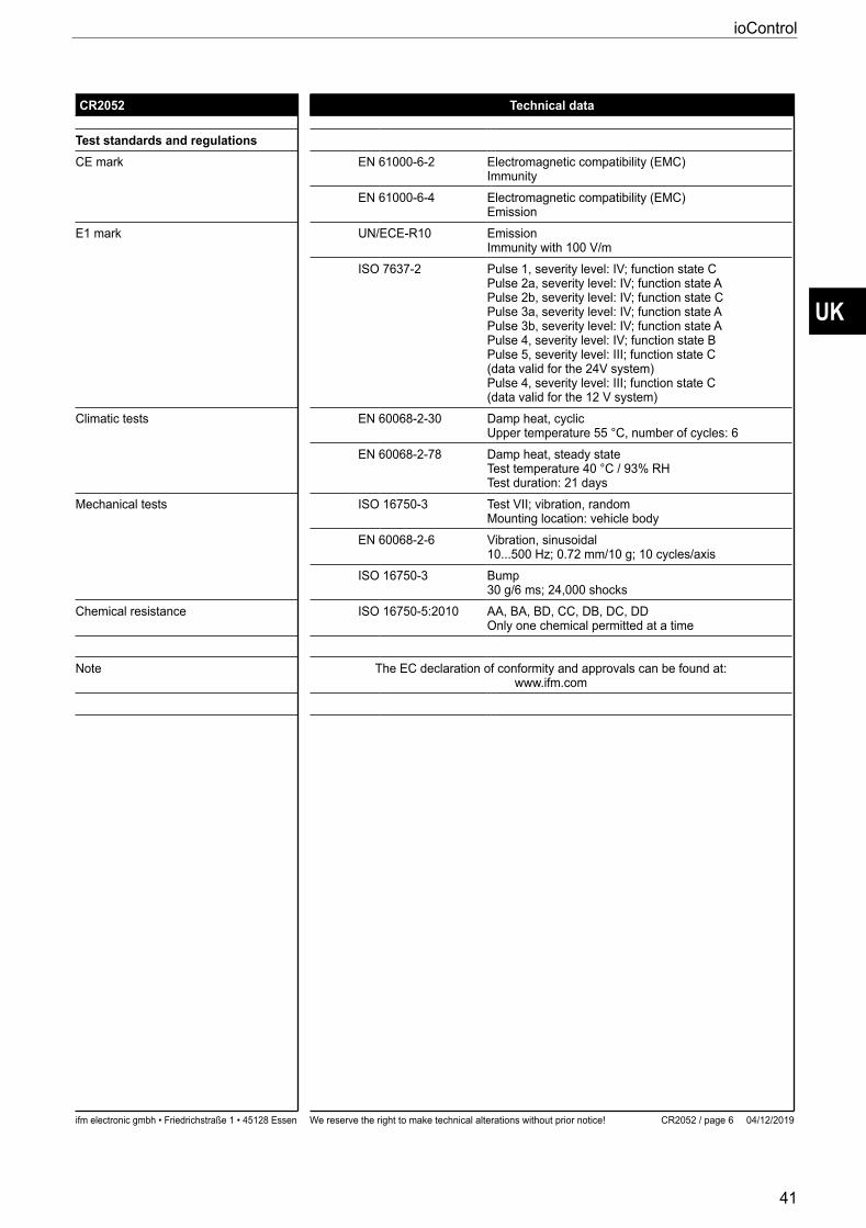
Test standards and regulationsCE mark EN 61000-6-2 Electromagnetic compatibility (EMC)
ImmunityEN 61000-6-4 Electromagnetic compatibility (EMC)
EmissionE1 mark UN/ECE-R10 Emission
Immunity with 100 V/mISO 7637-2 Pulse 1, severity level: IV; function state C
Pulse 2a, severity level: IV; function state APulse 2b, severity level: IV; function state CPulse 3a, severity level: IV; function state APulse 3b, severity level: IV; function state APulse 4, severity level: IV; function state BPulse 5, severity level: III; function state C(data valid for the 24V system)Pulse 4, severity level: III; function state C(data valid for the 12 V system)
Climatic tests EN 60068-2-30 Damp heat, cyclicUpper temperature 55 °C, number of cycles: 6
EN 60068-2-78 Damp heat, steady stateTest temperature 40 °C / 93% RHTest duration: 21 days
Mechanical tests ISO 16750-3 Test VII; vibration, randomMounting location: vehicle body
EN 60068-2-6 Vibration, sinusoidal10500 Hz; 072 mm/10 g; 10 cycles/axis
ISO 16750-3 Bump30 g/6 ms; 24,000 shocks
Chemical resistance ISO 16750-5:2010 AA, BA, BD, CC, DB, DC, DDOnly one chemical permitted at a time
Note The EC declaration of conformity and approvals can be found at:wwwifmcom
ioControl
42
ifm electronic gmbh • Friedrichstraße 1 • 45128 Essen We reserve the right to make technical alterations without prior notice! 04/12/2019CR2052 / page 7
CR2052 Technical data
Control systems
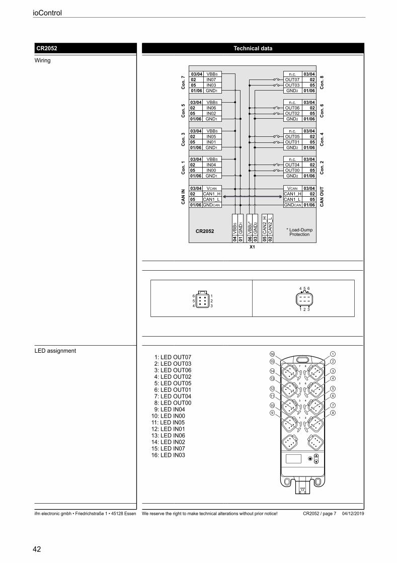
Wiring
Con
. 7
Con
. 8
CR2052 * Load-DumpProtection
03/04 VBBS
05IN07IN03
02
01/06 GND1
03/04
0502
01/06
n.c.OUT07OUT03GND2
Con
. 5
Con
. 6
03/04 VBBS
05IN06IN02
02
01/06 GND1
03/04
0502
01/06
n.c.OUT06OUT02GND2
Con
. 3
Con
. 4
03/04 VBBS
05IN05IN01
02
01/06 GND1
03/04
0502
01/06
n.c.OUT05OUT01GND2
Con
. 1
Con
. 2
03/04 VBBS
05IN04IN00
02
01/06 GND1
03/04
0502
01/06
n.c.OUT04OUT00
CA
N IN
CA
N O
UT03/04 VCAN
05CAN1_HCAN1_L
02
01/06 GNDCAN
VB
BS
06
GN
D1
VB
B2 *
0104
03/04
0502
01/06
GND2
VCAN
CAN1_HCAN1_LGNDCAN
03G
ND
2
05C
AN
2_H
02C
AN
2_L
X1
Original Scale Drawing (MTD)PIN_0193
456 1
23
456 1
23
EPS SourceFrame Size: 15 mm x 15 mm
50% 200%
Original Scale Drawing (MTD)
EPS SourceFrame Size: 15 mm x 15 mm
PIN_0196
4 5 6
1 2 3
4 5 6
1 2 3
LED assignment 1: LED OUT07 2: LED OUT03 3: LED OUT06 4: LED OUT02 5: LED OUT05 6: LED OUT01 7: LED OUT04 8: LED OUT00 9: LED IN0410: LED IN0011: LED IN0512: LED IN0113: LED IN0614: LED IN0215: LED IN0716: LED IN03
Original Scale Drawing (MTD)P_MZ_e100_0092
EPS SourceProduct Scale DrawingFrame Size: 80 mm x 90 mm
30% 333,4%
1
2
3
4
5
6
7
8
16
15
14
13
12
11
10
9
1 2
4
6
8
3
5
7
205,
523
4,2
76
52
17
6,9
8,7
6,9
1
2
3
27,411
40,5
4
5
1 2
4
6
8
3
5
7
UK
ioControl
43
ifm electronic gmbh • Friedrichstraße 1 • 45128 Essen We reserve the right to make technical alterations without prior notice! 04/12/2019CR2052 / page 8
CR2052 Technical data
Control systems
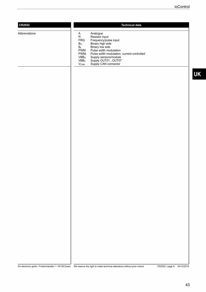
Abbreviations ARFRQBHBLPWMPWMIVBBS VBB2VCAN
AnalogueResistor inputFrequency/pulse inputBinary high sideBinary low sidePulse width modulationPulse width modulation, current-controlledSupply sensors/moduleSupply OUT01OUT07Supply CAN connector
ioControl
44
10 Maintenance, repair and disposalThe device is maintenance-free
Do not open the housing as the device does not contain any components which can be maintained by the user The device must only be repaired by the manufacturer
When the device is replaced, observe the pollution degree (→ 9 Technical data) until the protection rating is ensured by means of connectors/dummy plugs If necessary, clean the device/connector before the replacement Check the seals of the connectors for reusability The protection rating is only ensured for intact seals
Clean the device using a dry cloth
The following agents are not suited for cleaning the device: Chemicals dissolving plastics such as isopropanol, methylated spirit, benzine, thinner, alcohol, acetone or ammonia
Dispose of the device in accordance with the national environmental regulations
11 Approvals/standardsTest standards and regulations (→ 9 Technical data)The EU declaration of conformity and approvals can be found at: wwwifmcom
UK
ioControl
45
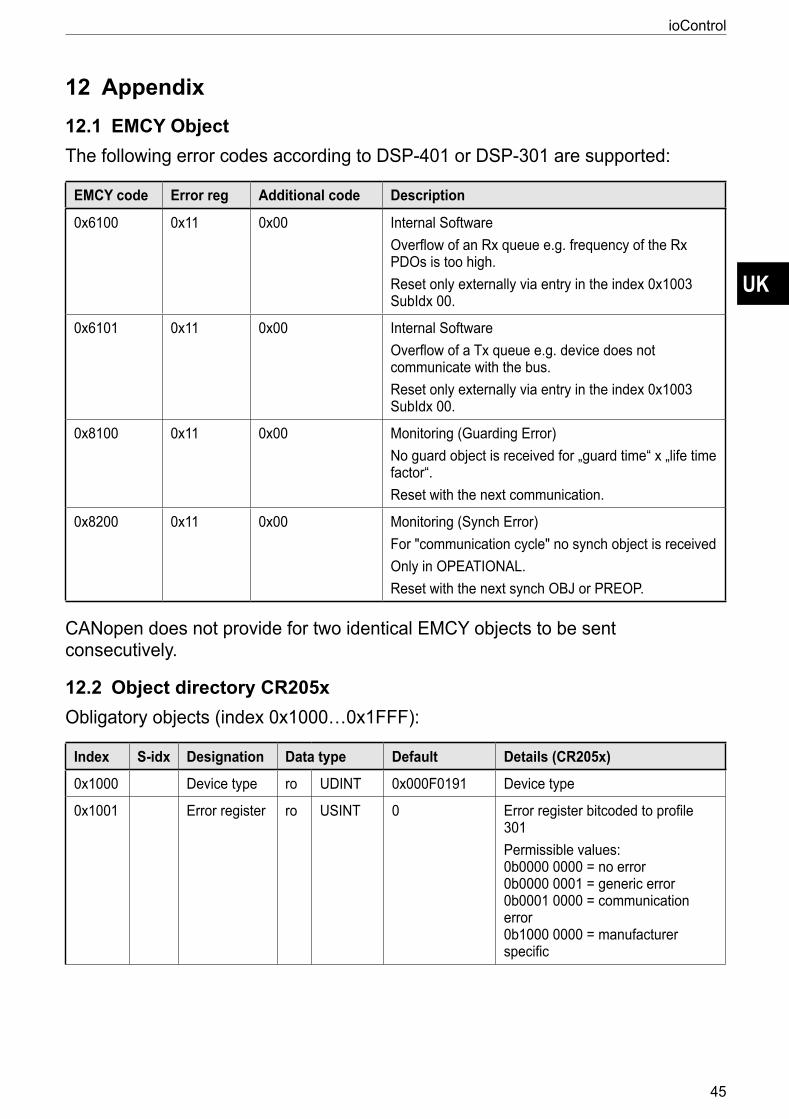
12 Appendix12.1 EMCY ObjectThe following error codes according to DSP-401 or DSP-301 are supported:
EMCY code Error reg Additional code Description
0x6100 0x11 0x00 Internal SoftwareOverflow of an Rx queue eg frequency of the Rx PDOs is too highReset only externally via entry in the index 0x1003 SubIdx 00
0x6101 0x11 0x00 Internal SoftwareOverflow of a Tx queue eg device does not communicate with the busReset only externally via entry in the index 0x1003 SubIdx 00
0x8100 0x11 0x00 Monitoring (Guarding Error)No guard object is received for „guard time“ x „life time factor“Reset with the next communication
0x8200 0x11 0x00 Monitoring (Synch Error)For "communication cycle" no synch object is receivedOnly in OPEATIONALReset with the next synch OBJ or PREOP
CANopen does not provide for two identical EMCY objects to be sent consecutively
12.2 Object directory CR205xObligatory objects (index 0x1000…0x1FFF):
Index S-idx Designation Data type Default Details (CR205x)
0x1000 Device type ro UDINT 0x000F0191 Device type
0x1001 Error register ro USINT 0 Error register bitcoded to profile 301Permissible values: 0b0000 0000 = no error 0b0000 0001 = generic error 0b0001 0000 = communication error 0b1000 0000 = manufacturer specific
ioControl
46
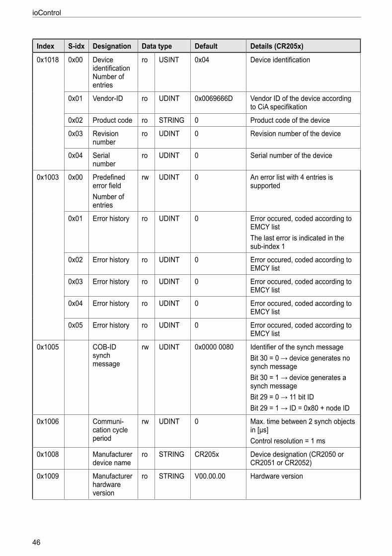
Index S-idx Designation Data type Default Details (CR205x)
0x1018 0x00 Device identification Number of entries
ro USINT 0x04 Device identification
0x01 Vendor-ID ro UDINT 0x0069666D Vendor ID of the device according to CiA specifikation
0x02 Product code ro STRING 0 Product code of the device
0x03 Revision number
ro UDINT 0 Revision number of the device
0x04 Serial number
ro UDINT 0 Serial number of the device
0x1003 0x00 Predefined error fieldNumber of entries
rw UDINT 0 An error list with 4 entries is supported
0x01 Error history ro UDINT 0 Error occured, coded according to EMCY listThe last error is indicated in the sub-index 1
0x02 Error history ro UDINT 0 Error occured, coded according to EMCY list
0x03 Error history ro UDINT 0 Error occured, coded according to EMCY list
0x04 Error history ro UDINT 0 Error occured, coded according to EMCY list
0x05 Error history ro UDINT 0 Error occured, coded according to EMCY list
0x1005 COB-ID synch message
rw UDINT 0x0000 0080 Identifier of the synch messageBit 30 = 0 → device generates no synch messageBit 30 = 1 → device generates a synch messageBit 29 = 0 → 11 bit IDBit 29 = 1 → ID = 0x80 + node ID
0x1006 Communi-cation cycle period
rw UDINT 0 Max time between 2 synch objects in [µs]Control resolution = 1 ms
0x1008 Manufacturer device name
ro STRING CR205x Device designation (CR2050 or CR2051 or CR2052)
0x1009 Manufacturer hardware version
ro STRING V000000 Hardware version
UK
ioControl
47
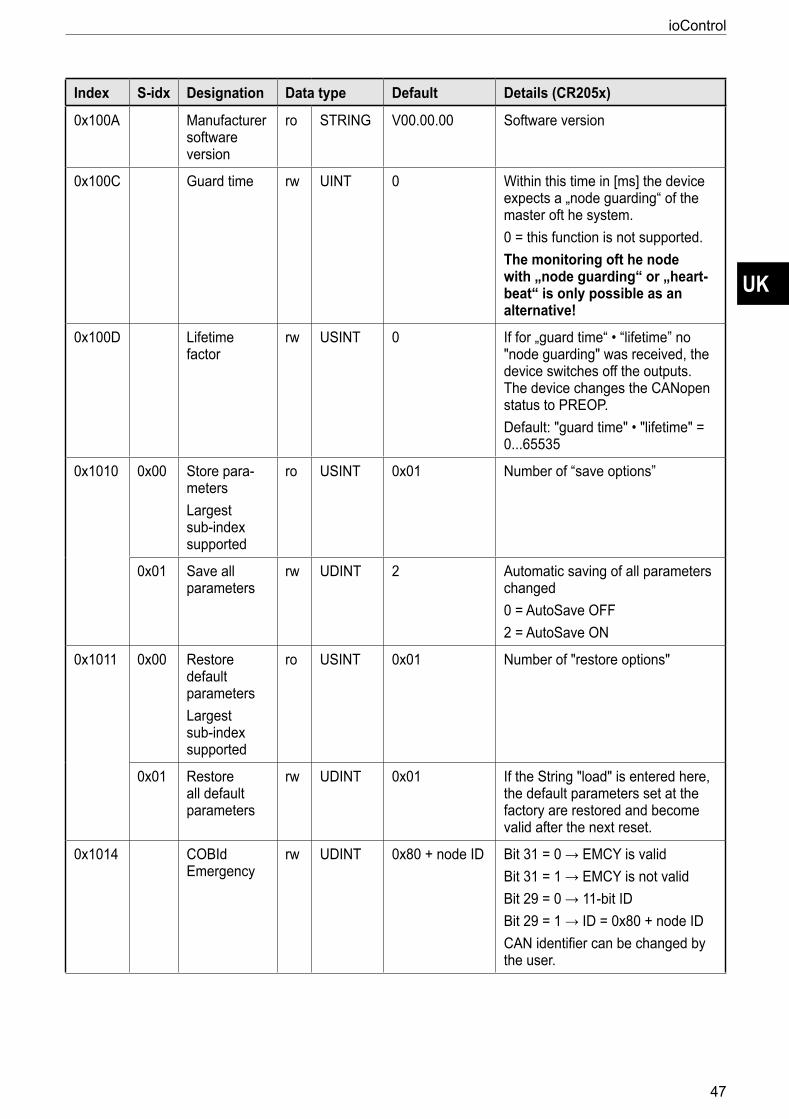
Index S-idx Designation Data type Default Details (CR205x)
0x100A Manufacturer software version
ro STRING V000000 Software version
0x100C Guard time rw UINT 0 Within this time in [ms] the device expects a „node guarding“ of the master oft he system0 = this function is not supportedThe monitoring oft he node with „node guarding“ or „heart-beat“ is only possible as an alternative!
0x100D Lifetime factor
rw USINT 0 If for „guard time“ • “lifetime” no "node guarding" was received, the device switches off the outputs The device changes the CANopen status to PREOPDefault: "guard time" • "lifetime" = 065535
0x1010 0x00 Store para-meters Largest sub-index supported
ro USINT 0x01 Number of “save options”
0x01 Save all parameters
rw UDINT 2 Automatic saving of all parameters changed0 = AutoSave OFF2 = AutoSave ON
0x1011 0x00 Restore default parametersLargest sub-index supported
ro USINT 0x01 Number of "restore options"
0x01 Restore all default parameters
rw UDINT 0x01 If the String "load" is entered here, the default parameters set at the factory are restored and become valid after the next reset
0x1014 COBId Emergency
rw UDINT 0x80 + node ID Bit 31 = 0 → EMCY is validBit 31 = 1 → EMCY is not validBit 29 = 0 → 11-bit IDBit 29 = 1 → ID = 0x80 + node IDCAN identifier can be changed by the user
ioControl
48
Index S-idx Designation Data type Default Details (CR205x)
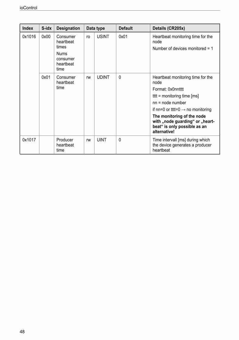
0x1016 0x00 Consumer heartbeat timesNums consumer heartbeat time
ro USINT 0x01 Heartbeat monitoring time for the node Number of devices monitored = 1
0x01 Consumer heartbeat time
rw UDINT 0 Heartbeat monitoring time for the nodeFormat: 0x0nntttttttt = monitoring time [ms]nn = node numberif nn=0 or tttt=0 → no monitoringThe monitoring of the node with „node guarding“ or „heart-beat“ is only possible as an alternative!
0x1017 Producer heartbeat time
rw UINT 0 Time intervall [ms] during which the device generates a producer heartbeat
UK
ioControl
49
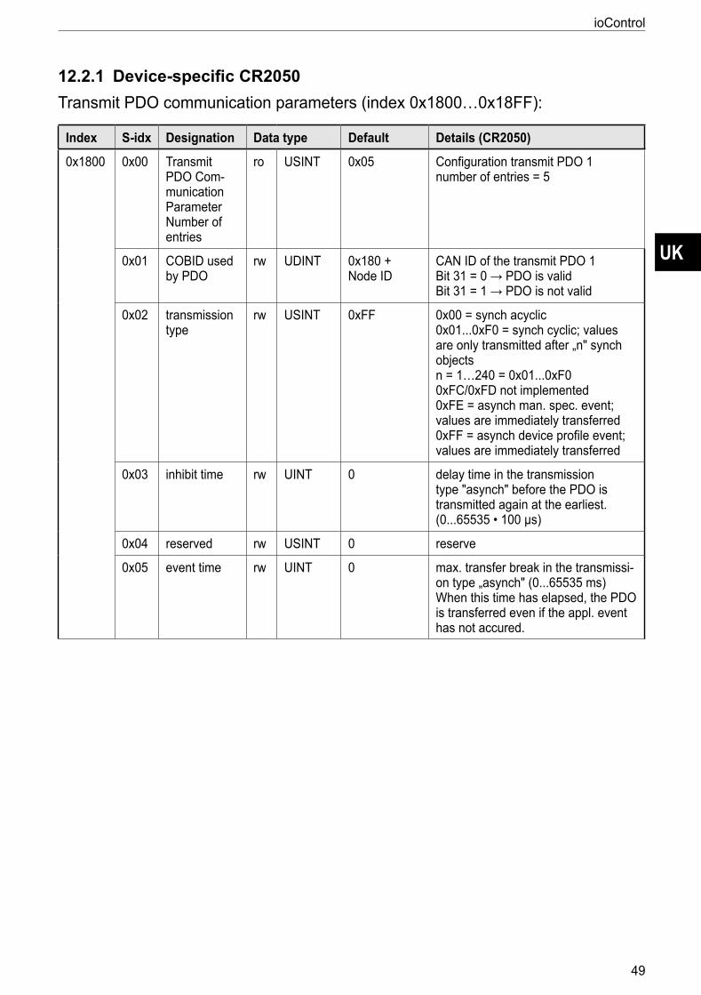
12.2.1 Device-specific CR2050Transmit PDO communication parameters (index 0x1800…0x18FF):
Index S-idx Designation Data type Default Details (CR2050)
0x1800 0x00 Transmit PDO Com-munication Parameter Number of entries
ro USINT 0x05 Configuration transmit PDO 1 number of entries = 5
0x01 COBID used by PDO
rw UDINT 0x180 + Node ID
CAN ID of the transmit PDO 1 Bit 31 = 0 → PDO is valid Bit 31 = 1 → PDO is not valid
0x02 transmission type
rw USINT 0xFF 0x00 = synch acyclic 0x010xF0 = synch cyclic; values are only transmitted after „n" synch objects n = 1…240 = 0x010xF0 0xFC/0xFD not implemented 0xFE = asynch man spec event; values are immediately transferred 0xFF = asynch device profile event; values are immediately transferred
0x03 inhibit time rw UINT 0 delay time in the transmission type "asynch" before the PDO is transmitted again at the earliest (065535 • 100 µs)
0x04 reserved rw USINT 0 reserve
0x05 event time rw UINT 0 max transfer break in the transmissi-on type „asynch" (065535 ms) When this time has elapsed, the PDO is transferred even if the appl event has not accured

ioControl
50
Index S-idx Designation Data type Default Details (CR2050)
0x1801 0x00 Transmit PDO Com-munication Parameter Number of entries
ro USINT 0x05 Configuration transmit PDO 2 number of entries = 5
0x01 COBID used by PDO
rw UDINT 0x280 + Node ID
CAN ID of the transmit PDO 2 Bit 31 = 0 → PDO is valid Bit 31 = 1 → PDO is not valid
0x02 transmission type
rw USINT 0x01 0x00 = synch acyclic 0x010xF0 = synch cyclic; values are only transmitted after „n" synch objects n = 1…240 = 0x010xF0 0xFC/0xFD not implemented 0xFE = asynch man spec event; values are immediately transferred 0xFF = asynch device profile event; values are immediately transferred
0x03 inhibit time rw UINT 0 delay time in the transmission type "asynch" before the PDO is transmitted again at the earliest (065535 • 100 µs)
0x04 reserved rw USINT 0 reserve
0x05 event time rw UINT 0 max transfer break in the transmissi-on type „asynch" (065535 ms) When this time has elapsed, the PDO is transferred even if the appl event has not accured

UK
ioControl
51
Index S-idx Designation Data type Default Details (CR2050)
0x1802 0x00 Transmit PDO Com-munication Parameter Number of entries
ro USINT 0x05 Configuration transmit PDO 3 number of entries = 5
0x01 COBID used by PDO
rw UDINT 0x380 + Node ID
CAN ID of the transmit PDO 3 Bit 31 = 0 → PDO is valid Bit 31 = 1 → PDO is not valid
0x02 transmission type
rw USINT 0x01 0x00 = synch acyclic 0x010xF0 = synch cyclic; values are only transmitted after „n" synch objects n = 1…240 = 0x010xF0 0xFC/0xFD not implemented 0xFE = asynch man spec event; values are immediately transferred 0xFF = asynch device profile event; values are immediately transferred
0x03 inhibit time rw UINT 0 delay time in the transmission type "asynch" before the PDO is transmitted again at the earliest (065535 • 100 µs)
0x04 reserved rw USINT 0 reserve
0x05 event time rw UINT 0 max transfer break in the transmissi-on type „asynch" (065535 ms) When this time has elapsed, the PDO is transferred even if the appl event has not accured
ioControl
52
Index S-idx Designation Data type Default Details (CR2050)
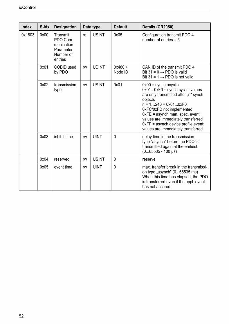
0x1803 0x00 Transmit PDO Com-munication Parameter Number of entries
ro USINT 0x05 Configuration transmit PDO 4 number of entries = 5
0x01 COBID used by PDO
rw UDINT 0x480 + Node ID
CAN ID of the transmit PDO 4 Bit 31 = 0 → PDO is valid Bit 31 = 1 → PDO is not valid
0x02 transmission type
rw USINT 0x01 0x00 = synch acyclic 0x010xF0 = synch cyclic; values are only transmitted after „n" synch objects n = 1…240 = 0x010xF0 0xFC/0xFD not implemented 0xFE = asynch man spec event; values are immediately transferred 0xFF = asynch device profile event; values are immediately transferred
0x03 inhibit time rw UINT 0 delay time in the transmission type "asynch" before the PDO is transmitted again at the earliest (065535 • 100 µs)
0x04 reserved rw USINT 0 reserve
0x05 event time rw UINT 0 max transfer break in the transmissi-on type „asynch" (065535 ms) When this time has elapsed, the PDO is transferred even if the appl event has not accured

UK
ioControl
53
Index S-idx Designation Data type Default Details (CR2050)
0x1804 0x00 Transmit PDO Com-munication Parameter Number of entries
ro USINT 0x05 Configuration transmit PDO 5 number of entries = 5
0x01 COBID used by PDO
rw UDINT 0x181 + Node ID
CAN ID of the transmit PDO 5 Bit 31 = 0 → PDO is valid Bit 31 = 1 → PDO is not valid
0x02 transmission type
rw USINT 0x01 0x00 = synch acyclic 0x010xF0 = synch cyclic; values are only transmitted after „n" synch objects n = 1…240 = 0x010xF0 0xFC/0xFD not implemented 0xFE = asynch man spec event; values are immediately transferred 0xFF = asynch device profile event; values are immediately transferred
0x03 inhibit time rw UINT 0 delay time in the transmission type "asynch" before the PDO is transmitted again at the earliest (065535 • 100 µs)
0x04 reserved rw USINT 0 reserve
0x05 event time rw UINT 0 max transfer break in the transmissi-on type „asynch" (065535 ms) When this time has elapsed, the PDO is transferred even if the appl event has not accured

ioControl
54
Index S-idx Designation Data type Default Details (CR2050)
0x1805 0x00 Transmit PDO Com-munication Parameter Number of entries
ro USINT 0x05 Configuration transmit PDO 6 number of entries = 5
0x01 COBID used by PDO
rw UDINT 0x281 + Node ID
CAN ID of the transmit PDO 6 Bit 31 = 0 → PDO is valid Bit 31 = 1 → PDO is not valid
0x02 transmission type
rw USINT 0x01 0x00 = synch acyclic 0x010xF0 = synch cyclic; values are only transmitted after „n" synch objects n = 1…240 = 0x010xF0 0xFC/0xFD not implemented 0xFE = asynch man spec event; values are immediately transferred 0xFF = asynch device profile event; values are immediately transferred
0x03 inhibit time rw UINT 0 delay time in the transmission type "asynch" before the PDO is transmitted again at the earliest (065535 • 100 µs)
0x04 reserved rw USINT 0 reserve
0x05 event time rw UINT 0 max transfer break in the transmissi-on type „asynch" (065535 ms) When this time has elapsed, the PDO is transferred even if the appl event has not accured

UK
ioControl
55
Index S-idx Designation Data type Default Details (CR2050)
0x1806 0x00 Transmit PDO Com-munication Parameter Number of entries
ro USINT 0x05 Configuration transmit PDO 7 number of entries = 5
0x01 COBID used by PDO
rw UDINT 0x381 + Node ID
CAN ID of the transmit PDO 7 Bit 31 = 0 → PDO is valid Bit 31 = 1 → PDO is not valid
0x02 transmission type
rw USINT 0x01 0x00 = synch acyclic 0x010xF0 = synch cyclic; values are only transmitted after „n" synch objects n = 1…240 = 0x010xF0 0xFC/0xFD not implemented 0xFE = asynch man spec event; values are immediately transferred 0xFF = asynch device profile event; values are immediately transferred
0x03 inhibit time rw UINT 0 delay time in the transmission type "asynch" before the PDO is transmitted again at the earliest (065535 • 100 µs)
0x04 reserved rw USINT 0 reserve
0x05 event time rw UINT 0 max transfer break in the transmissi-on type „asynch" (065535 ms) When this time has elapsed, the PDO is transferred even if the appl event has not accured

ioControl
56
Index S-idx Designation Data type Default Details (CR2050)
0x1807 0x00 Transmit PDO Com-munication Parameter Number of entries
ro USINT 0x05 Configuration transmit PDO 8 number of entries = 5
0x01 COBID used by PDO
rw UDINT 0x481 + Node ID
CAN ID of the transmit PDO 8 Bit 31 = 0 → PDO is valid Bit 31 = 1 → PDO is not valid
0x02 transmission type
rw USINT 0x01 0x00 = synch acyclic 0x010xF0 = synch cyclic; values are only transmitted after „n" synch objects n = 1…240 = 0x010xF0 0xFC/0xFD not implemented 0xFE = asynch man spec event; values are immediately transferred 0xFF = asynch device profile event; values are immediately transferred
0x03 inhibit time rw UINT 0 delay time in the transmission type "asynch" before the PDO is transmitted again at the earliest (065535 • 100 µs)
0x04 reserved rw USINT 0 reserve
0x05 event time rw UINT 0 max transfer break in the transmissi-on type „asynch" (065535 ms) When this time has elapsed, the PDO is transferred even if the appl event has not accured

UK
ioControl
57
Index S-idx Designation Data type Default Details (CR2050)
0x1808 0x00 Transmit PDO Com-munication Parameter Number of entries
ro USINT 0x05 Configuration transmit PDO 9 number of entries = 5
0x01 COBID used by PDO
rw UDINT 0x182 + Node ID
CAN ID of the transmit PDO 9 Bit 31 = 0 → PDO is valid Bit 31 = 1 → PDO is not valid
0x02 transmission type
rw USINT 0x01 0x00 = synch acyclic 0x010xF0 = synch cyclic; values are only transmitted after „n" synch objects n = 1…240 = 0x010xF0 0xFC/0xFD not implemented 0xFE = asynch man spec event; values are immediately transferred 0xFF = asynch device profile event; values are immediately transferred
0x03 inhibit time rw UINT 0 delay time in the transmission type "asynch" before the PDO is transmitted again at the earliest (065535 • 100 µs)
0x04 reserved rw USINT 0 reserve
0x05 event time rw UINT 0 max transfer break in the transmissi-on type „asynch" (065535 ms) When this time has elapsed, the PDO is transferred even if the appl event has not accured

ioControl
58
Index S-idx Designation Data type Default Details (CR2050)
0x1809 0x00 Transmit PDO Com-munication Parameter Number of entries
ro USINT 0x05 Configuration transmit PDO 10 number of entries = 5
0x01 COBID used by PDO
rw UDINT 0x282 + Node ID
CAN ID of the transmit PDO 10 Bit 31 = 0 → PDO is valid Bit 31 = 1 → PDO is not valid
0x02 transmission type
rw USINT 0x01 0x00 = synch acyclic 0x010xF0 = synch cyclic; values are only transmitted after „n" synch objects n = 1…240 = 0x010xF0 0xFC/0xFD not implemented 0xFE = asynch man spec event; values are immediately transferred 0xFF = asynch device profile event; values are immediately transferred
0x03 inhibit time rw UINT 0 delay time in the transmission type "asynch" before the PDO is transmitted again at the earliest (065535 • 100 µs)
0x04 reserved rw USINT 0 reserve
0x05 event time rw UINT 0 max transfer break in the transmissi-on type „asynch" (065535 ms) When this time has elapsed, the PDO is transferred even if the appl event has not accured

UK
ioControl
59
Transmit PDO mapping (index 0x1A00…0x1AFF):
Index S-idx Designation Data type Default Details (CR2050)
0x1A00 0x00 Transmit PDO map-ping Number of mapped objects in PDO
rw USINT 0x07 mapping transmit PDO 1 number of integrated application objects = 7
0x01 PDO map-ping
rw UDINT 0x6000 0108 Index 0x6000, SubIndex 0x01 binary inputs 0007: actual values (bit coded)
0x02 PDO map-ping
rw UDINT 0x6000 0208 Index 0x6000, SubIndex 0x02 binary inputs 08…15: actual values (bit coded)
0x03 PDO map-ping
rw UDINT 0x2020 0108 Index 0x2020, SubIndex 0x01 binary inputs 0007: flag "short circuit" (bit coded)
0x04 PDO map-ping
rw UDINT 0x2020 0208 Index 0x2020, SubIndex 0x02 binary inputs 08…15: flag "short circuit" (bit coded)
0x05 PDO map-ping
rw UDINT 0x2021 0108 Index 0x2021, SubIndex 0x01 outputs 0007: flag " wire break " (bit coded)
0x06 PDO map-ping
rw UDINT 0x2021 0208 Index 0x2021, SubIndex 0x02 outputs 08…15: flag " wire break " (bit coded)
0x07 PDO map-ping
rw UDINT 0x2025 0108 Index 0x2025, SubIndex 0x01 inputs 0003: flag " overload " (bit coded)
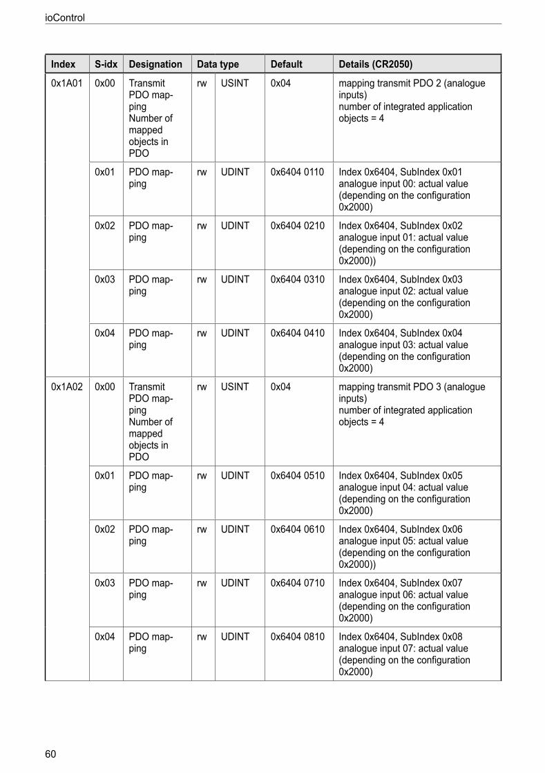
ioControl
60
Index S-idx Designation Data type Default Details (CR2050)
0x1A01 0x00 Transmit PDO map-ping Number of mapped objects in PDO
rw USINT 0x04 mapping transmit PDO 2 (analogue inputs) number of integrated application objects = 4
0x01 PDO map-ping
rw UDINT 0x6404 0110 Index 0x6404, SubIndex 0x01 analogue input 00: actual value (depending on the configuration 0x2000)
0x02 PDO map-ping
rw UDINT 0x6404 0210 Index 0x6404, SubIndex 0x02 analogue input 01: actual value (depending on the configuration 0x2000))
0x03 PDO map-ping
rw UDINT 0x6404 0310 Index 0x6404, SubIndex 0x03 analogue input 02: actual value (depending on the configuration 0x2000)
0x04 PDO map-ping
rw UDINT 0x6404 0410 Index 0x6404, SubIndex 0x04 analogue input 03: actual value (depending on the configuration 0x2000)
0x1A02 0x00 Transmit PDO map-ping Number of mapped objects in PDO
rw USINT 0x04 mapping transmit PDO 3 (analogue inputs) number of integrated application objects = 4
0x01 PDO map-ping
rw UDINT 0x6404 0510 Index 0x6404, SubIndex 0x05 analogue input 04: actual value (depending on the configuration 0x2000)
0x02 PDO map-ping
rw UDINT 0x6404 0610 Index 0x6404, SubIndex 0x06 analogue input 05: actual value (depending on the configuration 0x2000))
0x03 PDO map-ping
rw UDINT 0x6404 0710 Index 0x6404, SubIndex 0x07 analogue input 06: actual value (depending on the configuration 0x2000)
0x04 PDO map-ping
rw UDINT 0x6404 0810 Index 0x6404, SubIndex 0x08 analogue input 07: actual value (depending on the configuration 0x2000)
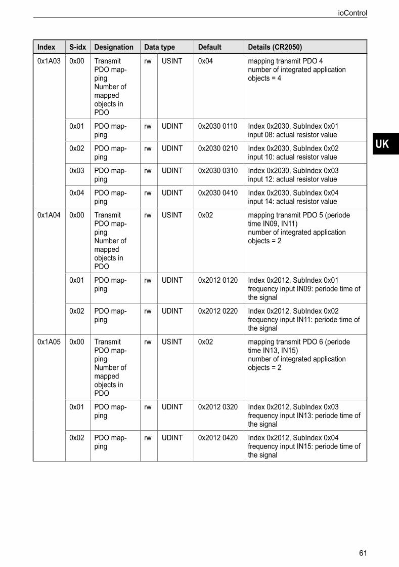
UK
ioControl
61
Index S-idx Designation Data type Default Details (CR2050)
0x1A03 0x00 Transmit PDO map-ping Number of mapped objects in PDO
rw USINT 0x04 mapping transmit PDO 4 number of integrated application objects = 4
0x01 PDO map-ping
rw UDINT 0x2030 0110 Index 0x2030, SubIndex 0x01 input 08: actual resistor value
0x02 PDO map-ping
rw UDINT 0x2030 0210 Index 0x2030, SubIndex 0x02 input 10: actual resistor value
0x03 PDO map-ping
rw UDINT 0x2030 0310 Index 0x2030, SubIndex 0x03 input 12: actual resistor value
0x04 PDO map-ping
rw UDINT 0x2030 0410 Index 0x2030, SubIndex 0x04 input 14: actual resistor value
0x1A04 0x00 Transmit PDO map-ping Number of mapped objects in PDO
rw USINT 0x02 mapping transmit PDO 5 (periode time IN09, IN11) number of integrated application objects = 2
0x01 PDO map-ping
rw UDINT 0x2012 0120 Index 0x2012, SubIndex 0x01 frequency input IN09: periode time of the signal
0x02 PDO map-ping
rw UDINT 0x2012 0220 Index 0x2012, SubIndex 0x02 frequency input IN11: periode time of the signal
0x1A05 0x00 Transmit PDO map-ping Number of mapped objects in PDO
rw USINT 0x02 mapping transmit PDO 6 (periode time IN13, IN15) number of integrated application objects = 2
0x01 PDO map-ping
rw UDINT 0x2012 0320 Index 0x2012, SubIndex 0x03 frequency input IN13: periode time of the signal
0x02 PDO map-ping
rw UDINT 0x2012 0420 Index 0x2012, SubIndex 0x04 frequency input IN15: periode time of the signal
ioControl
62
Index S-idx Designation Data type Default Details (CR2050)
0x1A06 0x00 Transmit PDO map-ping Number of mapped objects in PDO
rw USINT 0x04 mapping transmit PDO 7 (duty cycle of the signal on the frequency input IN09, IN11, IN13, IN15) number of integrated application objects = 4
0x01 PDO map-ping
rw UDINT 0x2014 0110 Index 0x2014, SubIndex 0x01 frequency input IN09: duty cycle of the signal in ‰
0x02 PDO map-ping
rw UDINT 0x2014 0210 Index 0x2014, SubIndex 0x02 frequency input IN11: duty cycle of the signal in ‰
0x03 PDO map-ping
rw UDINT 0x2014 0310 Index 0x2014, SubIndex 0x03 frequency input IN13: duty cycle of the signal in ‰
0x04 PDO map-ping
rw UDINT 0x2014 0410 Index 0x2014, SubIndex 0x04 frequency input IN15: duty cycle of the signal in ‰
0x1A07 0x00 Transmit PDO map-ping Number of mapped objects in PDO
rw USINT 0x02 mapping transmit PDO 8 (frequency on IN09, IN11) number of integrated application objects = 2
0x01 PDO map-ping
rw UDINT 0x2015 0120 Index 0x2015, SubIndex 0x01 frequency input IN09: frequency value of the signal in Hz
0x02 PDO map-ping
rw UDINT 0x2015 0220 Index 0x2015, SubIndex 0x02 frequency input IN11: frequency value of the signal in Hz
0x1A08 0x00 Transmit PDO map-ping Number of mapped objects in PDO
rw USINT 0x02 mapping transmit PDO 9 (frequency on IN13, IN15) number of integrated application objects = 2
0x01 PDO map-ping
rw UDINT 0x2015 0320 Index 0x2015, SubIndex 0x03 frequency input IN13: frequency value of the signal in Hz
0x02 PDO map-ping
rw UDINT 0x2015 0420 Index 0x2015, SubIndex 0x04 frequency input IN15: frequency value of the signal in Hz
UK
ioControl
63
Index S-idx Designation Data type Default Details (CR2050)
0x1A09 0x00 Transmit PDO map-ping Number of mapped objects in PDO
rw USINT 0x02 mapping transmit PDO 10 (system flag) number of integrated application objects = 2
0x01 PDO map-ping
rw UDINT 0x2040 0110 Index 0x2040, SubIndex 0x01 supply voltage of the system VBBS
0x02 PDO map-ping
rw UDINT 0x2050 0010 Index 0x2050, SubIndex 0x00 system temperature in °C
Manufacturer-specific objekts (index 0x20000x6FFF):
Index S-idx Designation Data type Default Details (CR2050)
0x2000 0x00 IO configu-ration Largest sub-index supported
ro USINT 16 Configuration inputs/outputs largest supported Sub-index = 32
0x01 Configuration IN00
rw USINT 10 0 = 0x00 3 = 0x03 6 = 0x06 7 = 0x07 9 = 0x09 10 = 0x0A 11 = 0x0B 12 = 0x0C
off Input IN00 010 000 mV ratiometric 01000 ‰ 020 000 µA 032 000 mV binary plus switched binary plus switched with diagnosis binary minus switched
0x02 Configuration IN01
rw USINT 10 0 = 0x00 3 = 0x03 6 = 0x06 7 = 0x07 9 = 0x09 10 = 0x0A 11 = 0x0B 12 = 0x0C
off Input IN01 010 000 mV ratiometric 01000 ‰ 020 000 µA 032 000 mV binary plus switched binary plus switched with diagnosis binary minus switched
0x03 Configuration IN02
rw USINT 10 0 = 0x00 3 = 0x03 6 = 0x06 7 = 0x07 9 = 0x09 10 = 0x0A 11 = 0x0B 12 = 0x0C
off Input IN02 010 000 mV ratiometric 01000 ‰ 020 000 µA 032 000 mV binary plus switched binary plus switched with diagnosis binary minus switched
ioControl
64
Index S-idx Designation Data type Default Details (CR2050)
0x2000 0x04 Configuration IN03
rw USINT 10 0 = 0x00 3 = 0x03 6 = 0x06 7 = 0x07 9 = 0x09 10 = 0x0A 11 = 0x0B 12 = 0x0C
off Input IN03 010 000 mV ratiometric 01000 ‰ 020 000 µA 032 000 mV binary plus switched binary plus switched with diagnosis binary minus switched
0x05 Configuration IN04
rw USINT 10 0 = 0x00 3 = 0x03 6 = 0x06 7 = 0x07 9 = 0x09 10 = 0x0A 11 = 0x0B 12 = 0x0C
off Input IN04 010 000 mV ratiometric 01000 ‰ 020 000 µA 032 000 mV binary plus switched binary plus switched with diagnosis binary minus switched
0x06 Configuration IN05
rw USINT 10 0 = 0x00 3 = 0x03 6 = 0x06 7 = 0x07 9 = 0x09 10 = 0x0A 11 = 0x0B 12 = 0x0C
off Input IN05 010 000 mV ratiometric 01000 ‰ 020 000 µA 032 000 mV binary plus switched binary plus switched with diagnosis binary minus switched
0x07 Configuration IN06
rw USINT 10 0 = 0x00 3 = 0x03 6 = 0x06 7 = 0x07 9 = 0x09 10 = 0x0A 11 = 0x0B 12 = 0x0C
off Input IN06 010 000 mV ratiometric 01000 ‰ 020 000 µA 032 000 mV binary plus switched binary plus switched with diagnosis binary minus switched
0x08 Configuration IN07
rw USINT 10 0 = 0x00 3 = 0x03 6 = 0x06 7 = 0x07 9 = 0x09 10 = 0x0A 11 = 0x0B 12 = 0x0C
off Input IN07 010 000 mV ratiometric 01000 ‰ 020 000 µA 032 000 mV binary plus switched binary plus switched with diagnosis binary minus switched
0x09 Configuration IN08
rw USINT 10 0 = 0x00 10 = 0x0A 11 = 0x0B 18 = 0x12
off Input IN08 binary plus switched binary plus switched with diagnosis 16…30 000 Ohm
UK
ioControl
65
Index S-idx Designation Data type Default Details (CR2050)
0x2000 0x0A Configuration IN09
rw USINT 01 0 = 0x00 01 = 0x01 14 = 0x0E 20 = 0x14
off Input IN09 binary plus switched frequency 0…30 000 Hz period duration
0x0B Configuration IN10
rw USINT 10 0 = 0x00 10 = 0x0A 11 = 0x0B 18 = 0x12
off Input IN10 binary plus switched binary plus switched with diagnosis 16…30 000 Ohm
0x0C Configuration IN11
rw USINT 01 0 = 0x00 01 = 0x01 14 = 0x0E 20 = 0x14
off Input IN11 binary plus switched frequency 0…30 000 Hz period duration
0x0D Configuration IN12
rw USINT 10 0 = 0x00 10 = 0x0A 11 = 0x0B 18 = 0x12
off Input IN12 binary plus switched binary plus switched with diagnosis 16…30 000 Ohm
0x0E Configuration IN13
rw USINT 01 0 = 0x00 01 = 0x01 14 = 0x0E 20 = 0x14
off Input IN12 binary plus switched frequency 0…30 000 Hz period duration
0x0F Configuration IN14
rw USINT 10 0 = 0x00 10 = 0x0A 11 = 0x0B 18 = 0x12
off Input IN14 binary plus switched binary plus switched with diagnosis 16…30 000 Ohm
0x10 Configuration IN15
rw USINT 01 0 = 0x00 01 = 0x01 14 = 0x0E 20 = 0x14
off Input IN15 binary plus switched frequency 0…30 000 Hz period duration
0x2012 0x00 Period input ro USINT 4 Largest sub-index supported
0x01 Period durati-on IN09
ro UDINT 0 IN09 period duration [µs]
0x02 Period durati-on IN11
ro UDINT 0 IN11 period duration [µs]
0x03 Period durati-on IN13
ro UDINT 0 IN13 period duration [µs]
0x04 Period durati-on IN15
ro UDINT 0 IN15 period duration [µs]
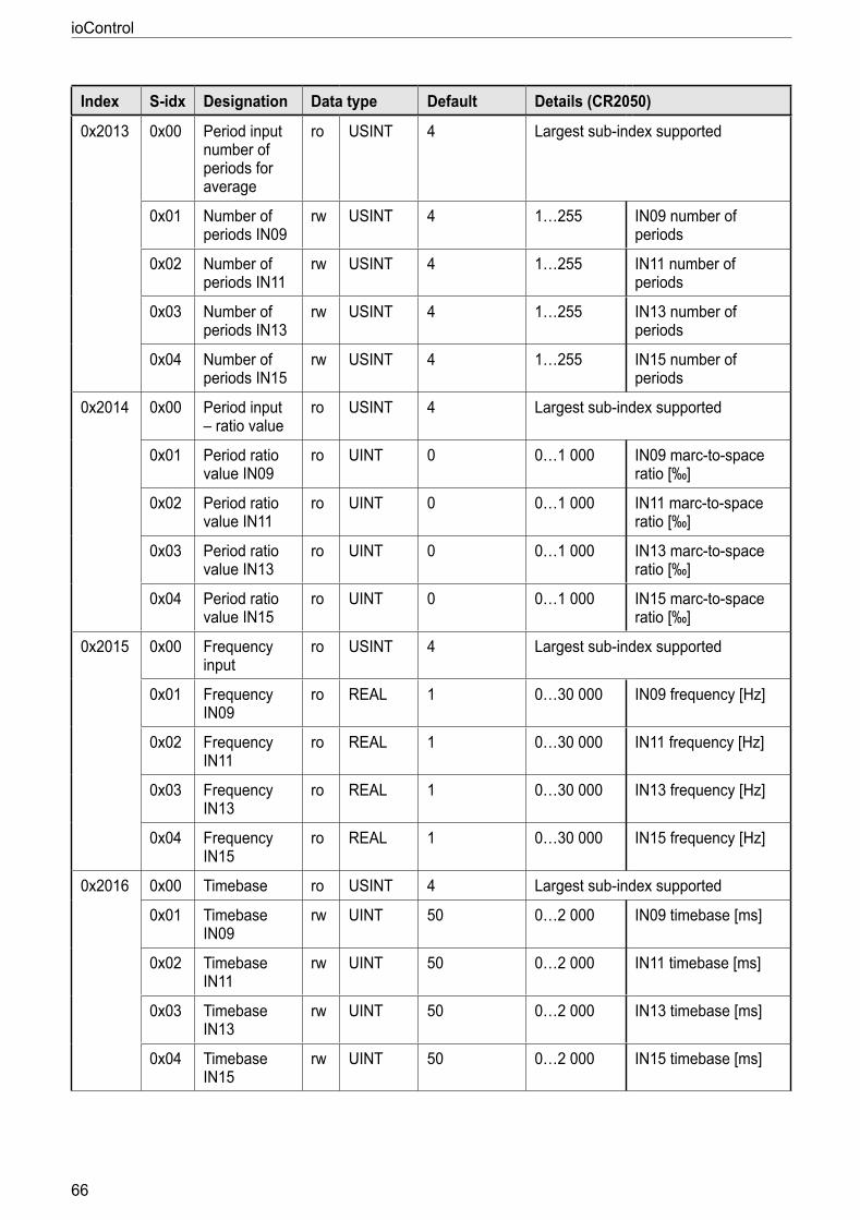
ioControl
66
Index S-idx Designation Data type Default Details (CR2050)
0x2013 0x00 Period input number of periods for average
ro USINT 4 Largest sub-index supported
0x01 Number of periods IN09
rw USINT 4 1…255 IN09 number of periods
0x02 Number of periods IN11
rw USINT 4 1…255 IN11 number of periods
0x03 Number of periods IN13
rw USINT 4 1…255 IN13 number of periods
0x04 Number of periods IN15
rw USINT 4 1…255 IN15 number of periods
0x2014 0x00 Period input – ratio value
ro USINT 4 Largest sub-index supported
0x01 Period ratio value IN09
ro UINT 0 0…1 000 IN09 marc-to-space ratio [‰]
0x02 Period ratio value IN11
ro UINT 0 0…1 000 IN11 marc-to-space ratio [‰]
0x03 Period ratio value IN13
ro UINT 0 0…1 000 IN13 marc-to-space ratio [‰]
0x04 Period ratio value IN15
ro UINT 0 0…1 000 IN15 marc-to-space ratio [‰]
0x2015 0x00 Frequency input
ro USINT 4 Largest sub-index supported
0x01 Frequency IN09
ro REAL 1 0…30 000 IN09 frequency [Hz]
0x02 Frequency IN11
ro REAL 1 0…30 000 IN11 frequency [Hz]
0x03 Frequency IN13
ro REAL 1 0…30 000 IN13 frequency [Hz]
0x04 Frequency IN15
ro REAL 1 0…30 000 IN15 frequency [Hz]
0x2016 0x00 Timebase ro USINT 4 Largest sub-index supported
0x01 Timebase IN09
rw UINT 50 0…2 000 IN09 timebase [ms]
0x02 Timebase IN11
rw UINT 50 0…2 000 IN11 timebase [ms]
0x03 Timebase IN13
rw UINT 50 0…2 000 IN13 timebase [ms]
0x04 Timebase IN15
rw UINT 50 0…2 000 IN15 timebase [ms]
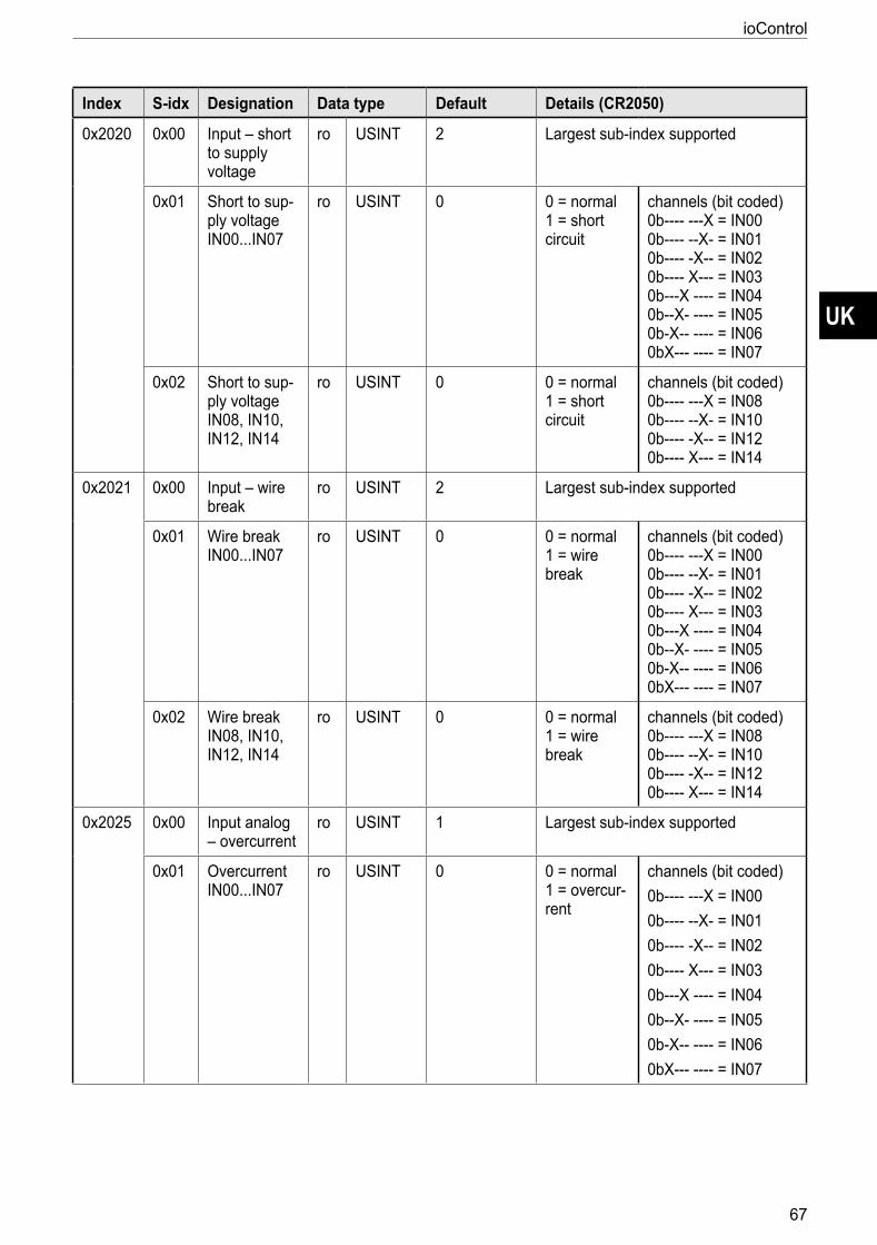
UK
ioControl
67
Index S-idx Designation Data type Default Details (CR2050)
0x2020 0x00 Input – short to supply voltage
ro USINT 2 Largest sub-index supported
0x01 Short to sup-ply voltage IN00IN07
ro USINT 0 0 = normal 1 = short circuit
channels (bit coded) 0b---- ---X = IN00 0b---- --X- = IN01 0b---- -X-- = IN02 0b---- X--- = IN03 0b---X ---- = IN04 0b--X- ---- = IN05 0b-X-- ---- = IN06 0bX--- ---- = IN07
0x02 Short to sup-ply voltage IN08, IN10, IN12, IN14
ro USINT 0 0 = normal 1 = short circuit
channels (bit coded) 0b---- ---X = IN08 0b---- --X- = IN10 0b---- -X-- = IN12 0b---- X--- = IN14
0x2021 0x00 Input – wire break
ro USINT 2 Largest sub-index supported
0x01 Wire break IN00IN07
ro USINT 0 0 = normal 1 = wire break
channels (bit coded) 0b---- ---X = IN00 0b---- --X- = IN01 0b---- -X-- = IN02 0b---- X--- = IN03 0b---X ---- = IN04 0b--X- ---- = IN05 0b-X-- ---- = IN06 0bX--- ---- = IN07
0x02 Wire break IN08, IN10, IN12, IN14
ro USINT 0 0 = normal 1 = wire break
channels (bit coded) 0b---- ---X = IN08 0b---- --X- = IN10 0b---- -X-- = IN12 0b---- X--- = IN14
0x2025 0x00 Input analog – overcurrent
ro USINT 1 Largest sub-index supported
0x01 Overcurrent IN00IN07
ro USINT 0 0 = normal 1 = overcur-rent
channels (bit coded) 0b---- ---X = IN000b---- --X- = IN010b---- -X-- = IN020b---- X--- = IN030b---X ---- = IN040b--X- ---- = IN050b-X-- ---- = IN060bX--- ---- = IN07
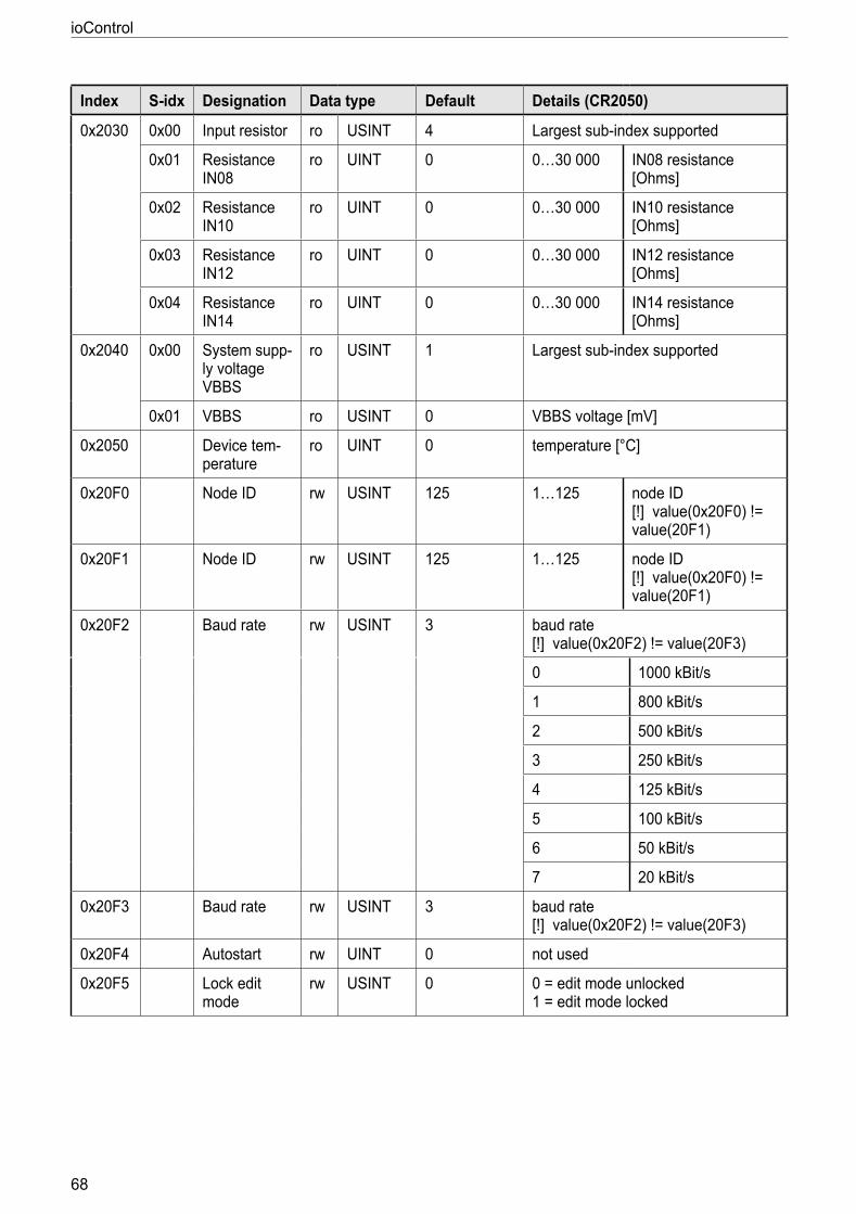
ioControl
68
Index S-idx Designation Data type Default Details (CR2050)
0x2030 0x00 Input resistor ro USINT 4 Largest sub-index supported
0x01 Resistance IN08
ro UINT 0 0…30 000 IN08 resistance [Ohms]
0x02 Resistance IN10
ro UINT 0 0…30 000 IN10 resistance [Ohms]
0x03 Resistance IN12
ro UINT 0 0…30 000 IN12 resistance [Ohms]
0x04 Resistance IN14
ro UINT 0 0…30 000 IN14 resistance [Ohms]
0x2040 0x00 System supp-ly voltage VBBS
ro USINT 1 Largest sub-index supported
0x01 VBBS ro USINT 0 VBBS voltage [mV]
0x2050 Device tem-perature
ro UINT 0 temperature [°C]
0x20F0 Node ID rw USINT 125 1…125 node ID [!] value(0x20F0) != value(20F1)
0x20F1 Node ID rw USINT 125 1…125 node ID [!] value(0x20F0) != value(20F1)
0x20F2 Baud rate rw USINT 3 baud rate [!] value(0x20F2) != value(20F3)
0 1000 kBit/s
1 800 kBit/s
2 500 kBit/s
3 250 kBit/s
4 125 kBit/s
5 100 kBit/s
6 50 kBit/s
7 20 kBit/s
0x20F3 Baud rate rw USINT 3 baud rate [!] value(0x20F2) != value(20F3)
0x20F4 Autostart rw UINT 0 not used
0x20F5 Lock edit mode
rw USINT 0 0 = edit mode unlocked 1 = edit mode locked
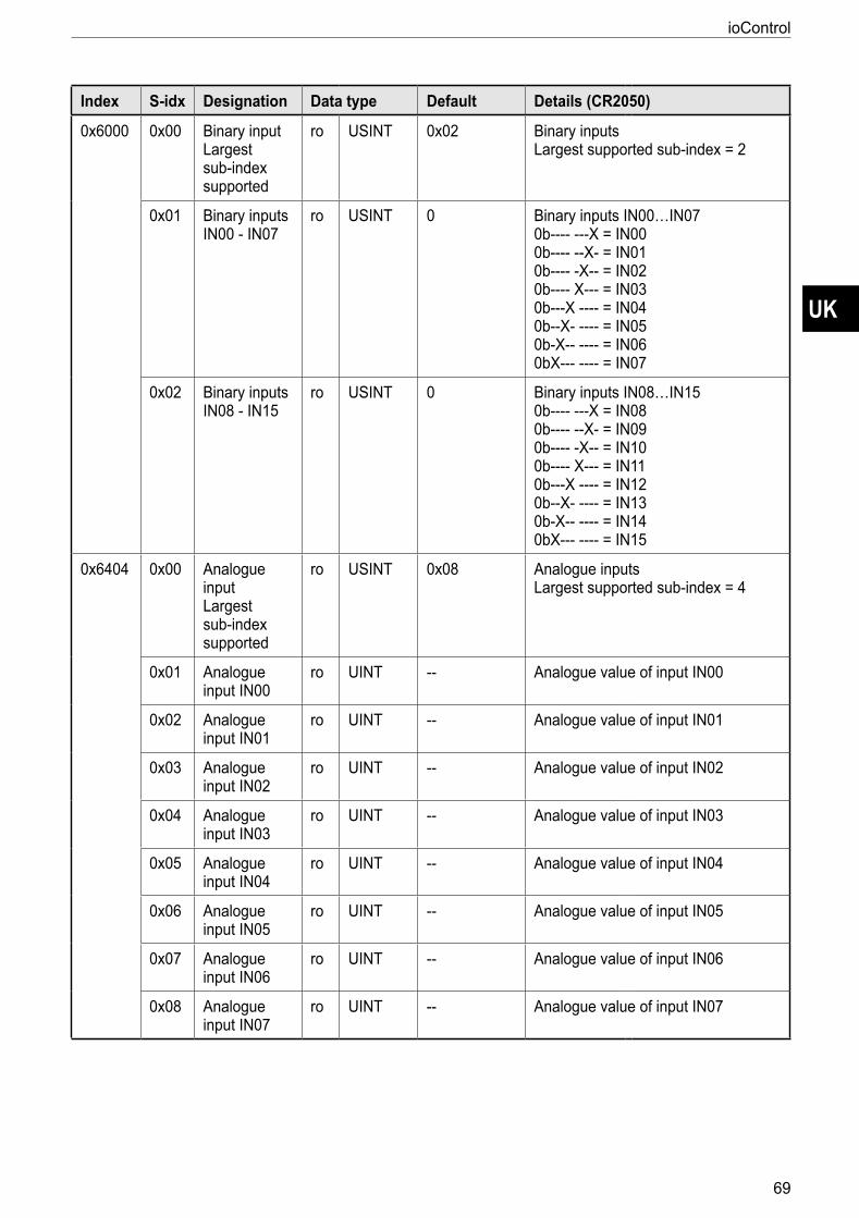
UK
ioControl
69
Index S-idx Designation Data type Default Details (CR2050)
0x6000 0x00 Binary input Largest sub-index supported
ro USINT 0x02 Binary inputs Largest supported sub-index = 2
0x01 Binary inputs IN00 - IN07
ro USINT 0 Binary inputs IN00…IN07 0b---- ---X = IN00 0b---- --X- = IN01 0b---- -X-- = IN02 0b---- X--- = IN03 0b---X ---- = IN04 0b--X- ---- = IN05 0b-X-- ---- = IN06 0bX--- ---- = IN07
0x02 Binary inputs IN08 - IN15
ro USINT 0 Binary inputs IN08…IN15 0b---- ---X = IN08 0b---- --X- = IN09 0b---- -X-- = IN10 0b---- X--- = IN11 0b---X ---- = IN12 0b--X- ---- = IN13 0b-X-- ---- = IN14 0bX--- ---- = IN15
0x6404 0x00 Analogue input Largest sub-index supported
ro USINT 0x08 Analogue inputs Largest supported sub-index = 4
0x01 Analogue input IN00
ro UINT -- Analogue value of input IN00
0x02 Analogue input IN01
ro UINT -- Analogue value of input IN01
0x03 Analogue input IN02
ro UINT -- Analogue value of input IN02
0x04 Analogue input IN03
ro UINT -- Analogue value of input IN03
0x05 Analogue input IN04
ro UINT -- Analogue value of input IN04
0x06 Analogue input IN05
ro UINT -- Analogue value of input IN05
0x07 Analogue input IN06
ro UINT -- Analogue value of input IN06
0x08 Analogue input IN07
ro UINT -- Analogue value of input IN07
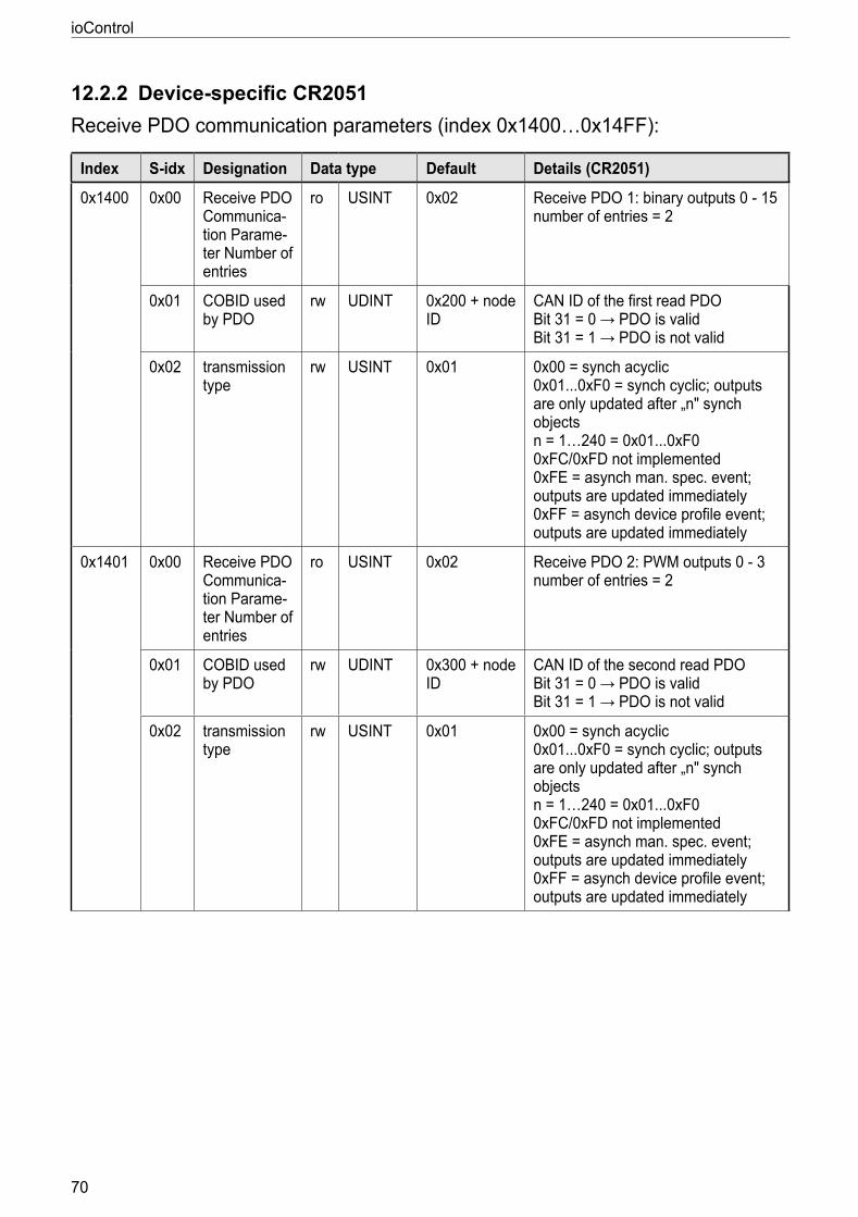
ioControl
70
12.2.2 Device-specific CR2051Receive PDO communication parameters (index 0x1400…0x14FF):
Index S-idx Designation Data type Default Details (CR2051)
0x1400 0x00 Receive PDO Communica-tion Parame-ter Number of entries
ro USINT 0x02 Receive PDO 1: binary outputs 0 - 15 number of entries = 2
0x01 COBID used by PDO
rw UDINT 0x200 + node ID
CAN ID of the first read PDO Bit 31 = 0 → PDO is valid Bit 31 = 1 → PDO is not valid
0x02 transmission type
rw USINT 0x01 0x00 = synch acyclic 0x010xF0 = synch cyclic; outputs are only updated after „n" synch objects n = 1…240 = 0x010xF0 0xFC/0xFD not implemented 0xFE = asynch man spec event; outputs are updated immediately 0xFF = asynch device profile event; outputs are updated immediately
0x1401 0x00 Receive PDO Communica-tion Parame-ter Number of entries
ro USINT 0x02 Receive PDO 2: PWM outputs 0 - 3 number of entries = 2
0x01 COBID used by PDO
rw UDINT 0x300 + node ID
CAN ID of the second read PDO Bit 31 = 0 → PDO is valid Bit 31 = 1 → PDO is not valid
0x02 transmission type
rw USINT 0x01 0x00 = synch acyclic 0x010xF0 = synch cyclic; outputs are only updated after „n" synch objects n = 1…240 = 0x010xF0 0xFC/0xFD not implemented 0xFE = asynch man spec event; outputs are updated immediately 0xFF = asynch device profile event; outputs are updated immediately
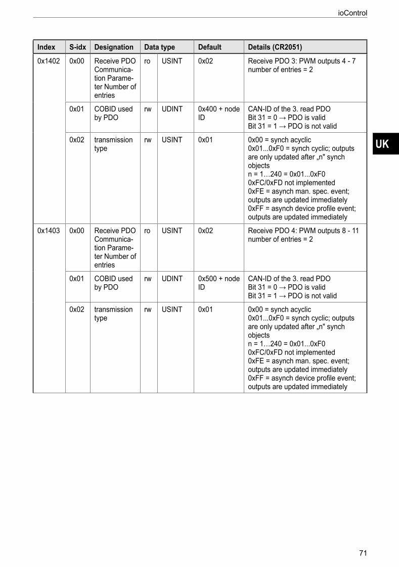
UK
ioControl
71
Index S-idx Designation Data type Default Details (CR2051)
0x1402 0x00 Receive PDO Communica-tion Parame-ter Number of entries
ro USINT 0x02 Receive PDO 3: PWM outputs 4 - 7 number of entries = 2
0x01 COBID used by PDO
rw UDINT 0x400 + node ID
CAN-ID of the 3 read PDO Bit 31 = 0 → PDO is valid Bit 31 = 1 → PDO is not valid
0x02 transmission type
rw USINT 0x01 0x00 = synch acyclic 0x010xF0 = synch cyclic; outputs are only updated after „n" synch objects n = 1…240 = 0x010xF0 0xFC/0xFD not implemented 0xFE = asynch man spec event; outputs are updated immediately 0xFF = asynch device profile event; outputs are updated immediately
0x1403 0x00 Receive PDO Communica-tion Parame-ter Number of entries
ro USINT 0x02 Receive PDO 4: PWM outputs 8 - 11 number of entries = 2
0x01 COBID used by PDO
rw UDINT 0x500 + node ID
CAN-ID of the 3 read PDO Bit 31 = 0 → PDO is valid Bit 31 = 1 → PDO is not valid
0x02 transmission type
rw USINT 0x01 0x00 = synch acyclic 0x010xF0 = synch cyclic; outputs are only updated after „n" synch objects n = 1…240 = 0x010xF0 0xFC/0xFD not implemented 0xFE = asynch man spec event; outputs are updated immediately 0xFF = asynch device profile event; outputs are updated immediately
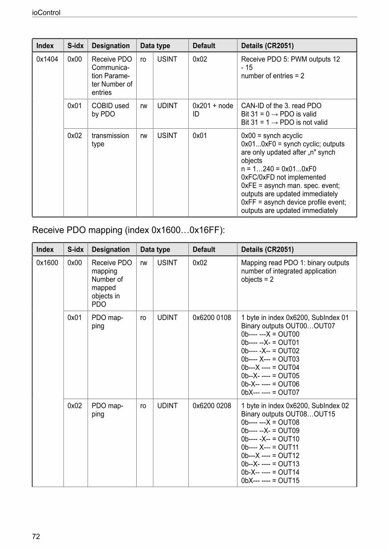
ioControl
72
Index S-idx Designation Data type Default Details (CR2051)
0x1404 0x00 Receive PDO Communica-tion Parame-ter Number of entries
ro USINT 0x02 Receive PDO 5: PWM outputs 12 - 15 number of entries = 2
0x01 COBID used by PDO
rw UDINT 0x201 + node ID
CAN-ID of the 3 read PDO Bit 31 = 0 → PDO is valid Bit 31 = 1 → PDO is not valid
0x02 transmission type
rw USINT 0x01 0x00 = synch acyclic 0x010xF0 = synch cyclic; outputs are only updated after „n" synch objects n = 1…240 = 0x010xF0 0xFC/0xFD not implemented 0xFE = asynch man spec event; outputs are updated immediately 0xFF = asynch device profile event; outputs are updated immediately
Receive PDO mapping (index 0x1600…0x16FF):
Index S-idx Designation Data type Default Details (CR2051)
0x1600 0x00 Receive PDO mapping Number of mapped objects in PDO
rw USINT 0x02 Mapping read PDO 1: binary outputs number of integrated application objects = 2
0x01 PDO map-ping
ro UDINT 0x6200 0108 1 byte in index 0x6200, SubIndex 01 Binary outputs OUT00…OUT07 0b---- ---X = OUT00 0b---- --X- = OUT01 0b---- -X-- = OUT02 0b---- X--- = OUT03 0b---X ---- = OUT04 0b--X- ---- = OUT05 0b-X-- ---- = OUT06 0bX--- ---- = OUT07
0x02 PDO map-ping
ro UDINT 0x6200 0208 1 byte in index 0x6200, SubIndex 02 Binary outputs OUT08…OUT15 0b---- ---X = OUT08 0b---- --X- = OUT09 0b---- -X-- = OUT10 0b---- X--- = OUT11 0b---X ---- = OUT12 0b--X- ---- = OUT13 0b-X-- ---- = OUT14 0bX--- ---- = OUT15

UK
ioControl
73
Index S-idx Designation Data type Default Details (CR2051)
0x1601 0x00 Receive PDO mapping Number of mapped objects in PDO
rw USINT 0x04 Mapping read PDO 2: PWM outputs OUT00…OUT03 number of integrated application objects = 4
0x01 PDO map-ping
rw UDINT 0x6414 0110 PWM/current output OUT00 Index 0x6414, SubIndex 0x01 contains the preset value of the PWM output OUT00, the value is interpreted as duty cycle in ‰ or as target current value (depending on the configuration index 0x2000)
0x02 PDO map-ping
rw UDINT 0x6414 0210 PWM/ current output OUT01 Index 0x6414, SubIndex 0x02 contains the preset value of the PWM output OUT01, the value is interpreted as duty cycle in ‰ or as target current value (depending on the configuration index 0x2000)
0x03 PDO map-ping
rw UDINT 0x6414 0310 PWM/ current output OUT02 Index 0x6414, SubIndex 0x03 contains the preset value of the PWM output OUT02, the value is interpreted as duty cycle in ‰ or as target current value (depending on the configuration index 0x2000)
0x04 PDO map-ping
rw UDINT 0x6414 0410 PWM/ current output OUT03 Index 0x6414, SubIndex 0x04 contains the preset value of the PWM output OUT03, the value is interpreted as duty cycle in ‰ or as target current value (depending on the configuration index 0x2000)
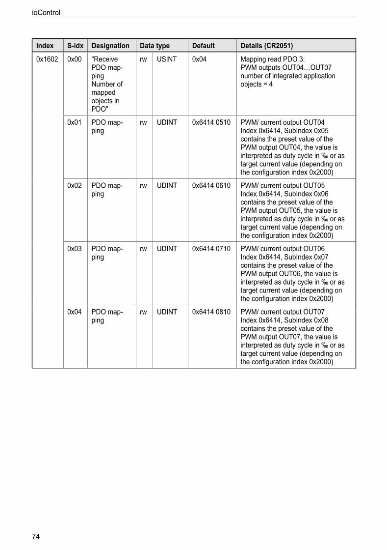
ioControl
74
Index S-idx Designation Data type Default Details (CR2051)
0x1602 0x00 "Receive PDO map-ping Number of mapped objects in PDO"
rw USINT 0x04 Mapping read PDO 3: PWM outputs OUT04…OUT07 number of integrated application objects = 4
0x01 PDO map-ping
rw UDINT 0x6414 0510 PWM/ current output OUT04 Index 0x6414, SubIndex 0x05 contains the preset value of the PWM output OUT04, the value is interpreted as duty cycle in ‰ or as target current value (depending on the configuration index 0x2000)
0x02 PDO map-ping
rw UDINT 0x6414 0610 PWM/ current output OUT05 Index 0x6414, SubIndex 0x06 contains the preset value of the PWM output OUT05, the value is interpreted as duty cycle in ‰ or as target current value (depending on the configuration index 0x2000)
0x03 PDO map-ping
rw UDINT 0x6414 0710 PWM/ current output OUT06 Index 0x6414, SubIndex 0x07 contains the preset value of the PWM output OUT06, the value is interpreted as duty cycle in ‰ or as target current value (depending on the configuration index 0x2000)
0x04 PDO map-ping
rw UDINT 0x6414 0810 PWM/ current output OUT07 Index 0x6414, SubIndex 0x08 contains the preset value of the PWM output OUT07, the value is interpreted as duty cycle in ‰ or as target current value (depending on the configuration index 0x2000)

UK
ioControl
75
Index S-idx Designation Data type Default Details (CR2051)
0x1603 0x00 Receive PDO mapping Number of mapped objects in PDO
rw USINT 0x04 Mapping read PDO 4: PWM outputs OUT08…OUT11 number of integrated application objects = 4
0x01 PDO map-ping
rw UDINT 0x6414 0910 PWM/ current output OUT08 Index 0x6414, SubIndex 0x09 contains the preset value of the PWM output OUT08, the value is interpreted as duty cycle in ‰ or as target current value (depending on the configuration index 0x2000)
0x02 PDO map-ping
rw UDINT 0x6414 0A10 PWM/ current output OUT09 Index 0x6414, SubIndex 0x0A contains the preset value of the PWM output OUT09, the value is interpreted as duty cycle in ‰ or as target current value (depending on the configuration index 0x2000)
0x03 PDO map-ping
rw UDINT 0x6414 0B10 PWM/ current output OUT10 Index 0x6414, SubIndex 0x0B contains the preset value of the PWM output OUT10, the value is interpreted as duty cycle in ‰ or as target current value (depending on the configuration index 0x2000)
0x04 PDO map-ping
rw UDINT 0x6414 0C10 PWM/ current output OUT11 Index 0x6414, SubIndex 0x0C contains the preset value of the PWM output OUT11, the value is interpreted as duty cycle in ‰ or as target current value (depending on the configuration index 0x2000)
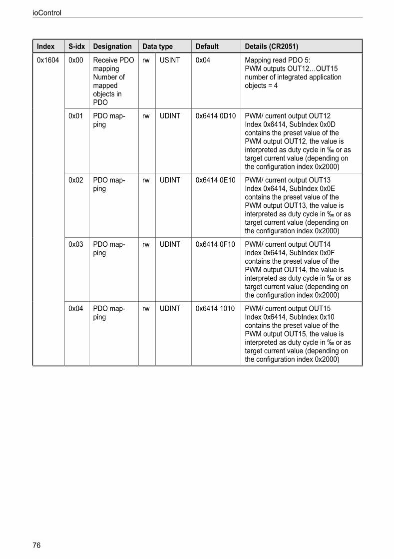
ioControl
76
Index S-idx Designation Data type Default Details (CR2051)
0x1604 0x00 Receive PDO mapping Number of mapped objects in PDO
rw USINT 0x04 Mapping read PDO 5: PWM outputs OUT12…OUT15 number of integrated application objects = 4
0x01 PDO map-ping
rw UDINT 0x6414 0D10 PWM/ current output OUT12 Index 0x6414, SubIndex 0x0D contains the preset value of the PWM output OUT12, the value is interpreted as duty cycle in ‰ or as target current value (depending on the configuration index 0x2000)
0x02 PDO map-ping
rw UDINT 0x6414 0E10 PWM/ current output OUT13 Index 0x6414, SubIndex 0x0E contains the preset value of the PWM output OUT13, the value is interpreted as duty cycle in ‰ or as target current value (depending on the configuration index 0x2000)
0x03 PDO map-ping
rw UDINT 0x6414 0F10 PWM/ current output OUT14 Index 0x6414, SubIndex 0x0F contains the preset value of the PWM output OUT14, the value is interpreted as duty cycle in ‰ or as target current value (depending on the configuration index 0x2000)
0x04 PDO map-ping
rw UDINT 0x6414 1010 PWM/ current output OUT15 Index 0x6414, SubIndex 0x10 contains the preset value of the PWM output OUT15, the value is interpreted as duty cycle in ‰ or as target current value (depending on the configuration index 0x2000)
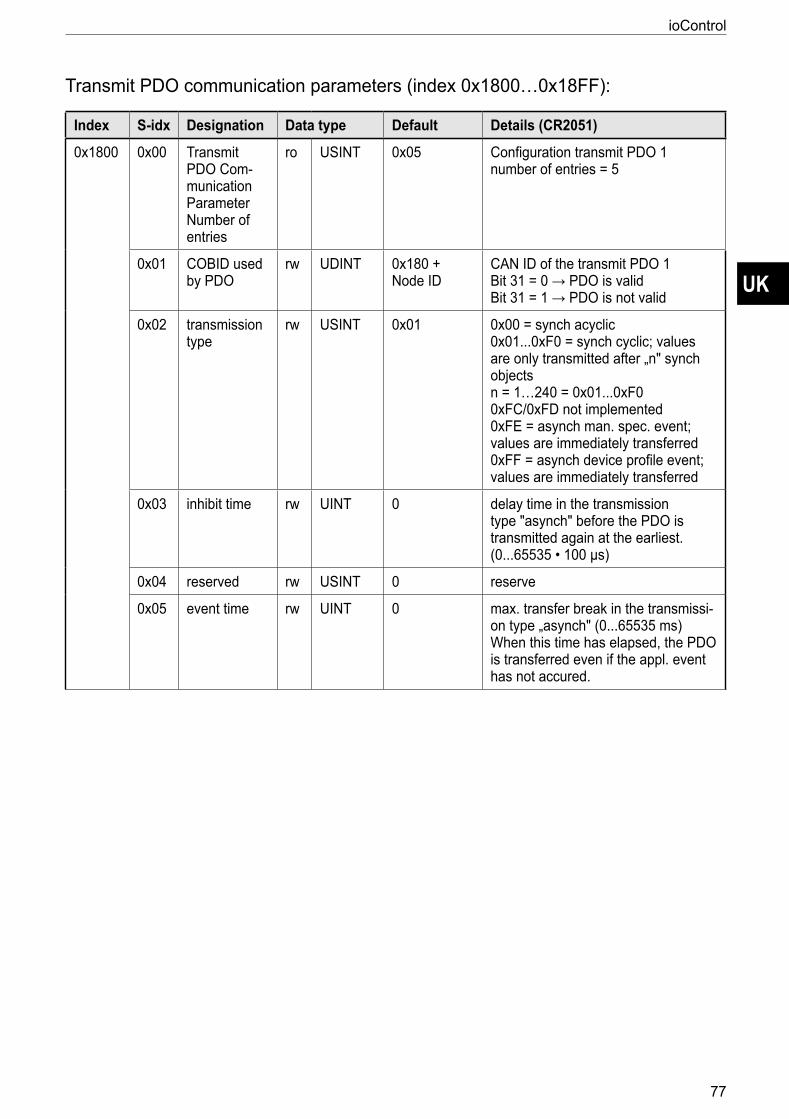
UK
ioControl
77
Transmit PDO communication parameters (index 0x1800…0x18FF):
Index S-idx Designation Data type Default Details (CR2051)
0x1800 0x00 Transmit PDO Com-munication Parameter Number of entries
ro USINT 0x05 Configuration transmit PDO 1 number of entries = 5
0x01 COBID used by PDO
rw UDINT 0x180 + Node ID
CAN ID of the transmit PDO 1 Bit 31 = 0 → PDO is valid Bit 31 = 1 → PDO is not valid
0x02 transmission type
rw USINT 0x01 0x00 = synch acyclic 0x010xF0 = synch cyclic; values are only transmitted after „n" synch objects n = 1…240 = 0x010xF0 0xFC/0xFD not implemented 0xFE = asynch man spec event; values are immediately transferred 0xFF = asynch device profile event; values are immediately transferred
0x03 inhibit time rw UINT 0 delay time in the transmission type "asynch" before the PDO is transmitted again at the earliest (065535 • 100 µs)
0x04 reserved rw USINT 0 reserve
0x05 event time rw UINT 0 max transfer break in the transmissi-on type „asynch" (065535 ms) When this time has elapsed, the PDO is transferred even if the appl event has not accured

ioControl
78
Index S-idx Designation Data type Default Details (CR2051)
0x1801 0x00 Transmit PDO Com-munication Parameter Number of entries
ro USINT 0x05 Configuration transmit PDO 2 number of entries = 5
0x01 COBID used by PDO
rw UDINT 0x280 + Node ID
CAN ID of the transmit PDO 2 Bit 31 = 0 → PDO is valid Bit 31 = 1 → PDO is not valid
0x02 transmission type
rw USINT 0x01 0x00 = synch acyclic 0x010xF0 = synch cyclic; values are only transmitted after „n" synch objects n = 1…240 = 0x010xF0 0xFC/0xFD not implemented 0xFE = asynch man spec event; values are immediately transferred 0xFF = asynch device profile event; values are immediately transferred
0x03 inhibit time rw UINT 0 delay time in the transmission type "asynch" before the PDO is transmitted again at the earliest (065535 • 100 µs)
0x04 reserved rw USINT 0 reserve
0x05 event time rw UINT 0 max transfer break in the transmissi-on type „asynch" (065535 ms) When this time has elapsed, the PDO is transferred even if the appl event has not accured

UK
ioControl
79
Index S-idx Designation Data type Default Details (CR2051)
0x1802 0x00 Transmit PDO Com-munication Parameter Number of entries
ro USINT 0x05 Configuration transmit PDO 3 number of entries = 5
0x01 COBID used by PDO
rw UDINT 0x380 + Node ID
CAN ID of the transmit PDO 3 Bit 31 = 0 → PDO is valid Bit 31 = 1 → PDO is not valid
0x02 transmission type
rw USINT 0x01 0x00 = synch acyclic 0x010xF0 = synch cyclic; values are only transmitted after „n" synch objects n = 1…240 = 0x010xF0 0xFC/0xFD not implemented 0xFE = asynch man spec event; values are immediately transferred 0xFF = asynch device profile event; values are immediately transferred
0x03 inhibit time rw UINT 0 delay time in the transmission type "asynch" before the PDO is transmitted again at the earliest (065535 • 100 µs)
0x04 reserved rw USINT 0 reserve
0x05 event time rw UINT 0 max transfer break in the transmissi-on type „asynch" (065535 ms) When this time has elapsed, the PDO is transferred even if the appl event has not accured

ioControl
80
Index S-idx Designation Data type Default Details (CR2051)
0x1803 0x00 Transmit PDO Com-munication Parameter Number of entries
ro USINT 0x05 Configuration transmit PDO 4 number of entries = 5
0x01 COBID used by PDO
rw UDINT 0x480 + Node ID
CAN ID of the transmit PDO 4 Bit 31 = 0 → PDO is valid Bit 31 = 1 → PDO is not valid
0x02 transmission type
rw USINT 0x01 0x00 = synch acyclic 0x010xF0 = synch cyclic; values are only transmitted after „n" synch objects n = 1…240 = 0x010xF0 0xFC/0xFD not implemented 0xFE = asynch man spec event; values are immediately transferred 0xFF = asynch device profile event; values are immediately transferred
0x03 inhibit time rw UINT 0 delay time in the transmission type "asynch" before the PDO is transmitted again at the earliest (065535 • 100 µs)
0x04 reserved rw USINT 0 reserve
0x05 event time rw UINT 0 max transfer break in the transmissi-on type „asynch" (065535 ms) When this time has elapsed, the PDO is transferred even if the appl event has not accured
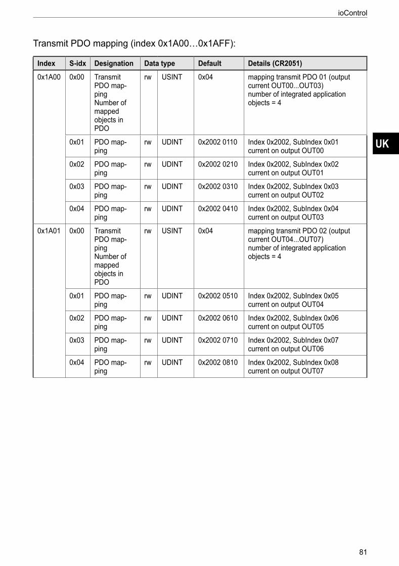
UK
ioControl
81
Transmit PDO mapping (index 0x1A00…0x1AFF):
Index S-idx Designation Data type Default Details (CR2051)
0x1A00 0x00 Transmit PDO map-ping Number of mapped objects in PDO
rw USINT 0x04 mapping transmit PDO 01 (output current OUT00OUT03) number of integrated application objects = 4
0x01 PDO map-ping
rw UDINT 0x2002 0110 Index 0x2002, SubIndex 0x01 current on output OUT00
0x02 PDO map-ping
rw UDINT 0x2002 0210 Index 0x2002, SubIndex 0x02 current on output OUT01
0x03 PDO map-ping
rw UDINT 0x2002 0310 Index 0x2002, SubIndex 0x03 current on output OUT02
0x04 PDO map-ping
rw UDINT 0x2002 0410 Index 0x2002, SubIndex 0x04 current on output OUT03
0x1A01 0x00 Transmit PDO map-ping Number of mapped objects in PDO
rw USINT 0x04 mapping transmit PDO 02 (output current OUT04OUT07) number of integrated application objects = 4
0x01 PDO map-ping
rw UDINT 0x2002 0510 Index 0x2002, SubIndex 0x05 current on output OUT04
0x02 PDO map-ping
rw UDINT 0x2002 0610 Index 0x2002, SubIndex 0x06 current on output OUT05
0x03 PDO map-ping
rw UDINT 0x2002 0710 Index 0x2002, SubIndex 0x07 current on output OUT06
0x04 PDO map-ping
rw UDINT 0x2002 0810 Index 0x2002, SubIndex 0x08 current on output OUT07
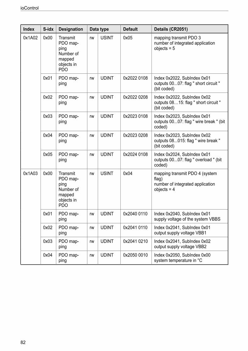
ioControl
82
Index S-idx Designation Data type Default Details (CR2051)
0x1A02 0x00 Transmit PDO map-ping Number of mapped objects in PDO
rw USINT 0x05 mapping transmit PDO 3 number of integrated application objects = 5
0x01 PDO map-ping
rw UDINT 0x2022 0108 Index 0x2022, SubIndex 0x01 outputs 0007: flag " short circuit " (bit coded)
0x02 PDO map-ping
rw UDINT 0x2022 0208 Index 0x2022, SubIndex 0x02 outputs 08…15: flag " short circuit " (bit coded)
0x03 PDO map-ping
rw UDINT 0x2023 0108 Index 0x2023, SubIndex 0x01 outputs 0007: flag " wire break " (bit coded)
0x04 PDO map-ping
rw UDINT 0x2023 0208 Index 0x2023, SubIndex 0x02 outputs 08015: flag " wire break " (bit coded)
0x05 PDO map-ping
rw UDINT 0x2024 0108 Index 0x2024, SubIndex 0x01 outputs 0007: flag " overload " (bit coded)
0x1A03 0x00 Transmit PDO map-ping Number of mapped objects in PDO
rw USINT 0x04 mapping transmit PDO 4 (system flag) number of integrated application objects = 4
0x01 PDO map-ping
rw UDINT 0x2040 0110 Index 0x2040, SubIndex 0x01 supply voltage of the system VBBS
0x02 PDO map-ping
rw UDINT 0x2041 0110 Index 0x2041, SubIndex 0x01 output supply voltage VBB1
0x03 PDO map-ping
rw UDINT 0x2041 0210 Index 0x2041, SubIndex 0x02 output supply voltage VBB2
0x04 PDO map-ping
rw UDINT 0x2050 0010 Index 0x2050, SubIndex 0x00 system temperature in °C
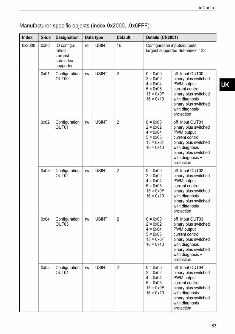
UK
ioControl
83
Manufacturer-specific objekts (index 0x20000x6FFF):
Index S-idx Designation Data type Default Details (CR2051)
0x2000 0x00 IO configu-ration Largest sub-index supported
ro USINT 16 Configuration inputs/outputs largest supported Sub-index = 32
0x01 Configuration OUT00
rw USINT 2 0 = 0x00 2 = 0x02 4 = 0x04 5 = 0x05 15 = 0x0F 16 = 0x10
off Input OUT00 binary plus switched PWM output current control binary plus switched with diagnosis binary plus switched with diagnosis + protection
0x02 Configuration OUT01
rw USINT 2 0 = 0x00 2 = 0x02 4 = 0x04 5 = 0x05 15 = 0x0F 16 = 0x10
off Input OUT01 binary plus switched PWM output current control binary plus switched with diagnosis binary plus switched with diagnosis + protection
0x03 Configuration OUT02
rw USINT 2 0 = 0x00 2 = 0x02 4 = 0x04 5 = 0x05 15 = 0x0F 16 = 0x10
off Input OUT02 binary plus switched PWM output current control binary plus switched with diagnosis binary plus switched with diagnosis + protection
0x04 Configuration OUT03
rw USINT 2 0 = 0x00 2 = 0x02 4 = 0x04 5 = 0x05 15 = 0x0F 16 = 0x10
off Input OUT03 binary plus switched PWM output current control binary plus switched with diagnosis binary plus switched with diagnosis + protection
0x05 Configuration OUT04
rw USINT 2 0 = 0x00 2 = 0x02 4 = 0x04 5 = 0x05 15 = 0x0F 16 = 0x10
off Input OUT04 binary plus switched PWM output current control binary plus switched with diagnosis binary plus switched with diagnosis + protection
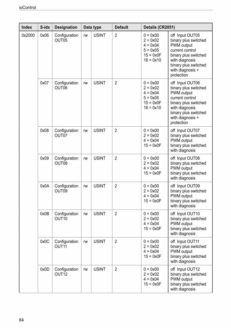
ioControl
84
Index S-idx Designation Data type Default Details (CR2051)
0x2000 0x06 Configuration OUT05
rw USINT 2 0 = 0x00 2 = 0x02 4 = 0x04 5 = 0x05 15 = 0x0F 16 = 0x10
off Input OUT05 binary plus switched PWM output current control binary plus switched with diagnosis binary plus switched with diagnosis + protection
0x07 Configuration OUT06
rw USINT 2 0 = 0x00 2 = 0x02 4 = 0x04 5 = 0x05 15 = 0x0F 16 = 0x10
off Input OUT06 binary plus switched PWM output current control binary plus switched with diagnosis binary plus switched with diagnosis + protection
0x08 Configuration OUT07
rw USINT 2 0 = 0x00 2 = 0x02 4 = 0x04 15 = 0x0F
off Input OUT07 binary plus switched PWM output binary plus switched with diagnosis
0x09 Configuration OUT08
rw USINT 2 0 = 0x00 2 = 0x02 4 = 0x04 15 = 0x0F
off Input OUT08 binary plus switched PWM output binary plus switched with diagnosis
0x0A Configuration OUT09
rw USINT 2 0 = 0x00 2 = 0x02 4 = 0x04 15 = 0x0F
off Input OUT09 binary plus switched PWM output binary plus switched with diagnosis
0x0B Configuration OUT10
rw USINT 2 0 = 0x00 2 = 0x02 4 = 0x04 15 = 0x0F
off Input OUT10 binary plus switched PWM output binary plus switched with diagnosis
0x0C Configuration OUT11
rw USINT 2 0 = 0x00 2 = 0x02 4 = 0x04 15 = 0x0F
off Input OUT11 binary plus switched PWM output binary plus switched with diagnosis
0x0D Configuration OUT12
rw USINT 2 0 = 0x00 2 = 0x02 4 = 0x04 15 = 0x0F
off Input OUT12 binary plus switched PWM output binary plus switched with diagnosis
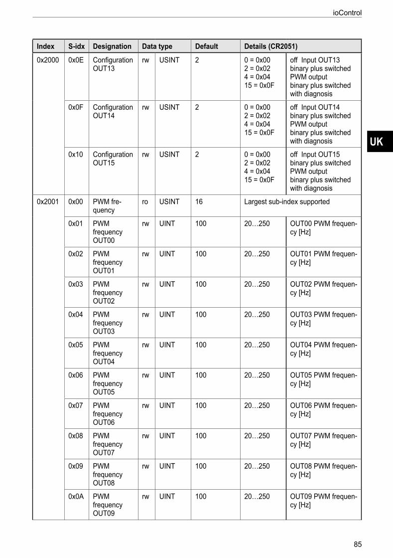
UK
ioControl
85
Index S-idx Designation Data type Default Details (CR2051)
0x2000 0x0E Configuration OUT13
rw USINT 2 0 = 0x00 2 = 0x02 4 = 0x04 15 = 0x0F
off Input OUT13 binary plus switched PWM output binary plus switched with diagnosis
0x0F Configuration OUT14
rw USINT 2 0 = 0x00 2 = 0x02 4 = 0x04 15 = 0x0F
off Input OUT14 binary plus switched PWM output binary plus switched with diagnosis
0x10 Configuration OUT15
rw USINT 2 0 = 0x00 2 = 0x02 4 = 0x04 15 = 0x0F
off Input OUT15 binary plus switched PWM output binary plus switched with diagnosis
0x2001 0x00 PWM fre-quency
ro USINT 16 Largest sub-index supported
0x01 PWM frequency OUT00
rw UINT 100 20…250 OUT00 PWM frequen-cy [Hz]
0x02 PWM frequency OUT01
rw UINT 100 20…250 OUT01 PWM frequen-cy [Hz]
0x03 PWM frequency OUT02
rw UINT 100 20…250 OUT02 PWM frequen-cy [Hz]
0x04 PWM frequency OUT03
rw UINT 100 20…250 OUT03 PWM frequen-cy [Hz]
0x05 PWM frequency OUT04
rw UINT 100 20…250 OUT04 PWM frequen-cy [Hz]
0x06 PWM frequency OUT05
rw UINT 100 20…250 OUT05 PWM frequen-cy [Hz]
0x07 PWM frequency OUT06
rw UINT 100 20…250 OUT06 PWM frequen-cy [Hz]
0x08 PWM frequency OUT07
rw UINT 100 20…250 OUT07 PWM frequen-cy [Hz]
0x09 PWM frequency OUT08
rw UINT 100 20…250 OUT08 PWM frequen-cy [Hz]
0x0A PWM frequency OUT09
rw UINT 100 20…250 OUT09 PWM frequen-cy [Hz]
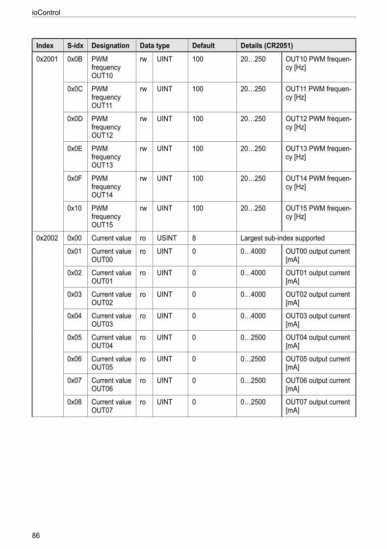
ioControl
86
Index S-idx Designation Data type Default Details (CR2051)
0x2001 0x0B PWM frequency OUT10
rw UINT 100 20…250 OUT10 PWM frequen-cy [Hz]
0x0C PWM frequency OUT11
rw UINT 100 20…250 OUT11 PWM frequen-cy [Hz]
0x0D PWM frequency OUT12
rw UINT 100 20…250 OUT12 PWM frequen-cy [Hz]
0x0E PWM frequency OUT13
rw UINT 100 20…250 OUT13 PWM frequen-cy [Hz]
0x0F PWM frequency OUT14
rw UINT 100 20…250 OUT14 PWM frequen-cy [Hz]
0x10 PWM frequency OUT15
rw UINT 100 20…250 OUT15 PWM frequen-cy [Hz]
0x2002 0x00 Current value ro USINT 8 Largest sub-index supported
0x01 Current value OUT00
ro UINT 0 0…4000 OUT00 output current [mA]
0x02 Current value OUT01
ro UINT 0 0…4000 OUT01 output current [mA]
0x03 Current value OUT02
ro UINT 0 0…4000 OUT02 output current [mA]
0x04 Current value OUT03
ro UINT 0 0…4000 OUT03 output current [mA]
0x05 Current value OUT04
ro UINT 0 0…2500 OUT04 output current [mA]
0x06 Current value OUT05
ro UINT 0 0…2500 OUT05 output current [mA]
0x07 Current value OUT06
ro UINT 0 0…2500 OUT06 output current [mA]
0x08 Current value OUT07
ro UINT 0 0…2500 OUT07 output current [mA]
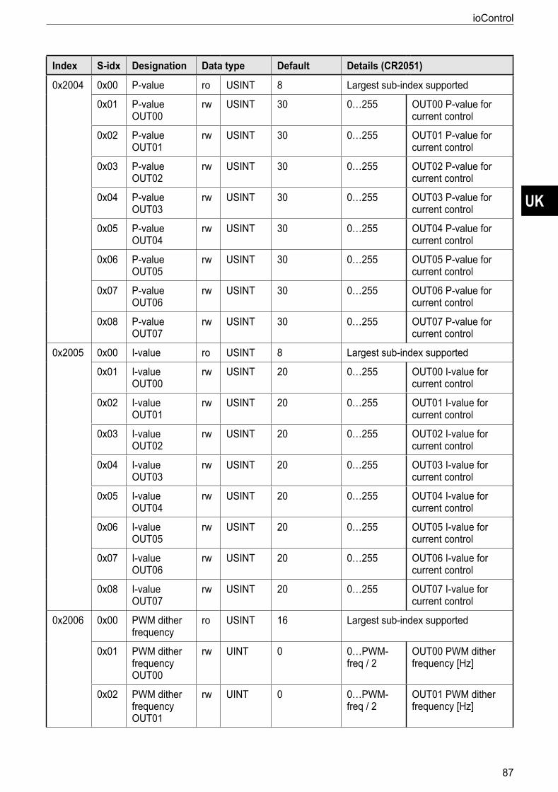
UK
ioControl
87
Index S-idx Designation Data type Default Details (CR2051)
0x2004 0x00 P-value ro USINT 8 Largest sub-index supported
0x01 P-value OUT00
rw USINT 30 0…255 OUT00 P-value for current control
0x02 P-value OUT01
rw USINT 30 0…255 OUT01 P-value for current control
0x03 P-value OUT02
rw USINT 30 0…255 OUT02 P-value for current control
0x04 P-value OUT03
rw USINT 30 0…255 OUT03 P-value for current control
0x05 P-value OUT04
rw USINT 30 0…255 OUT04 P-value for current control
0x06 P-value OUT05
rw USINT 30 0…255 OUT05 P-value for current control
0x07 P-value OUT06
rw USINT 30 0…255 OUT06 P-value for current control
0x08 P-value OUT07
rw USINT 30 0…255 OUT07 P-value for current control
0x2005 0x00 I-value ro USINT 8 Largest sub-index supported
0x01 I-value OUT00
rw USINT 20 0…255 OUT00 I-value for current control
0x02 I-value OUT01
rw USINT 20 0…255 OUT01 I-value for current control
0x03 I-value OUT02
rw USINT 20 0…255 OUT02 I-value for current control
0x04 I-value OUT03
rw USINT 20 0…255 OUT03 I-value for current control
0x05 I-value OUT04
rw USINT 20 0…255 OUT04 I-value for current control
0x06 I-value OUT05
rw USINT 20 0…255 OUT05 I-value for current control
0x07 I-value OUT06
rw USINT 20 0…255 OUT06 I-value for current control
0x08 I-value OUT07
rw USINT 20 0…255 OUT07 I-value for current control
0x2006 0x00 PWM dither frequency
ro USINT 16 Largest sub-index supported
0x01 PWM dither frequency OUT00
rw UINT 0 0…PWM-freq / 2
OUT00 PWM dither frequency [Hz]
0x02 PWM dither frequency OUT01
rw UINT 0 0…PWM-freq / 2
OUT01 PWM dither frequency [Hz]
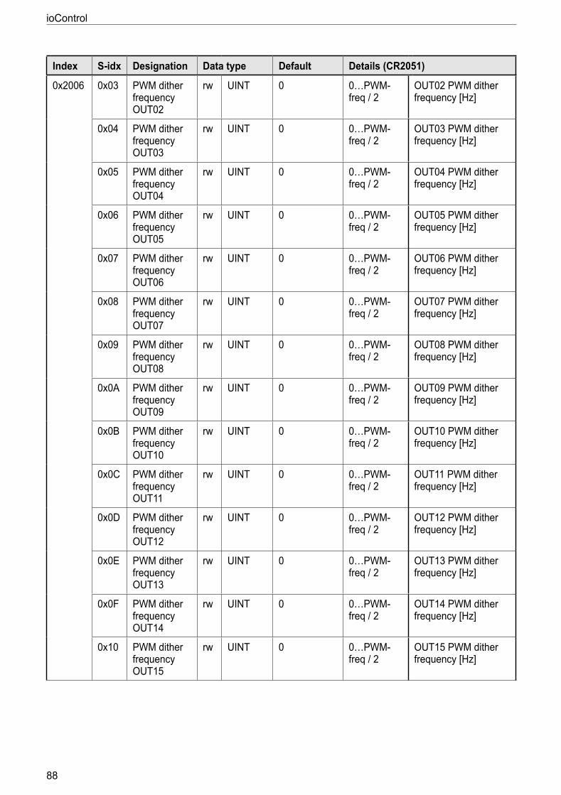
ioControl
88
Index S-idx Designation Data type Default Details (CR2051)
0x2006 0x03 PWM dither frequency OUT02
rw UINT 0 0…PWM-freq / 2
OUT02 PWM dither frequency [Hz]
0x04 PWM dither frequency OUT03
rw UINT 0 0…PWM-freq / 2
OUT03 PWM dither frequency [Hz]
0x05 PWM dither frequency OUT04
rw UINT 0 0…PWM-freq / 2
OUT04 PWM dither frequency [Hz]
0x06 PWM dither frequency OUT05
rw UINT 0 0…PWM-freq / 2
OUT05 PWM dither frequency [Hz]
0x07 PWM dither frequency OUT06
rw UINT 0 0…PWM-freq / 2
OUT06 PWM dither frequency [Hz]
0x08 PWM dither frequency OUT07
rw UINT 0 0…PWM-freq / 2
OUT07 PWM dither frequency [Hz]
0x09 PWM dither frequency OUT08
rw UINT 0 0…PWM-freq / 2
OUT08 PWM dither frequency [Hz]
0x0A PWM dither frequency OUT09
rw UINT 0 0…PWM-freq / 2
OUT09 PWM dither frequency [Hz]
0x0B PWM dither frequency OUT10
rw UINT 0 0…PWM-freq / 2
OUT10 PWM dither frequency [Hz]
0x0C PWM dither frequency OUT11
rw UINT 0 0…PWM-freq / 2
OUT11 PWM dither frequency [Hz]
0x0D PWM dither frequency OUT12
rw UINT 0 0…PWM-freq / 2
OUT12 PWM dither frequency [Hz]
0x0E PWM dither frequency OUT13
rw UINT 0 0…PWM-freq / 2
OUT13 PWM dither frequency [Hz]
0x0F PWM dither frequency OUT14
rw UINT 0 0…PWM-freq / 2
OUT14 PWM dither frequency [Hz]
0x10 PWM dither frequency OUT15
rw UINT 0 0…PWM-freq / 2
OUT15 PWM dither frequency [Hz]
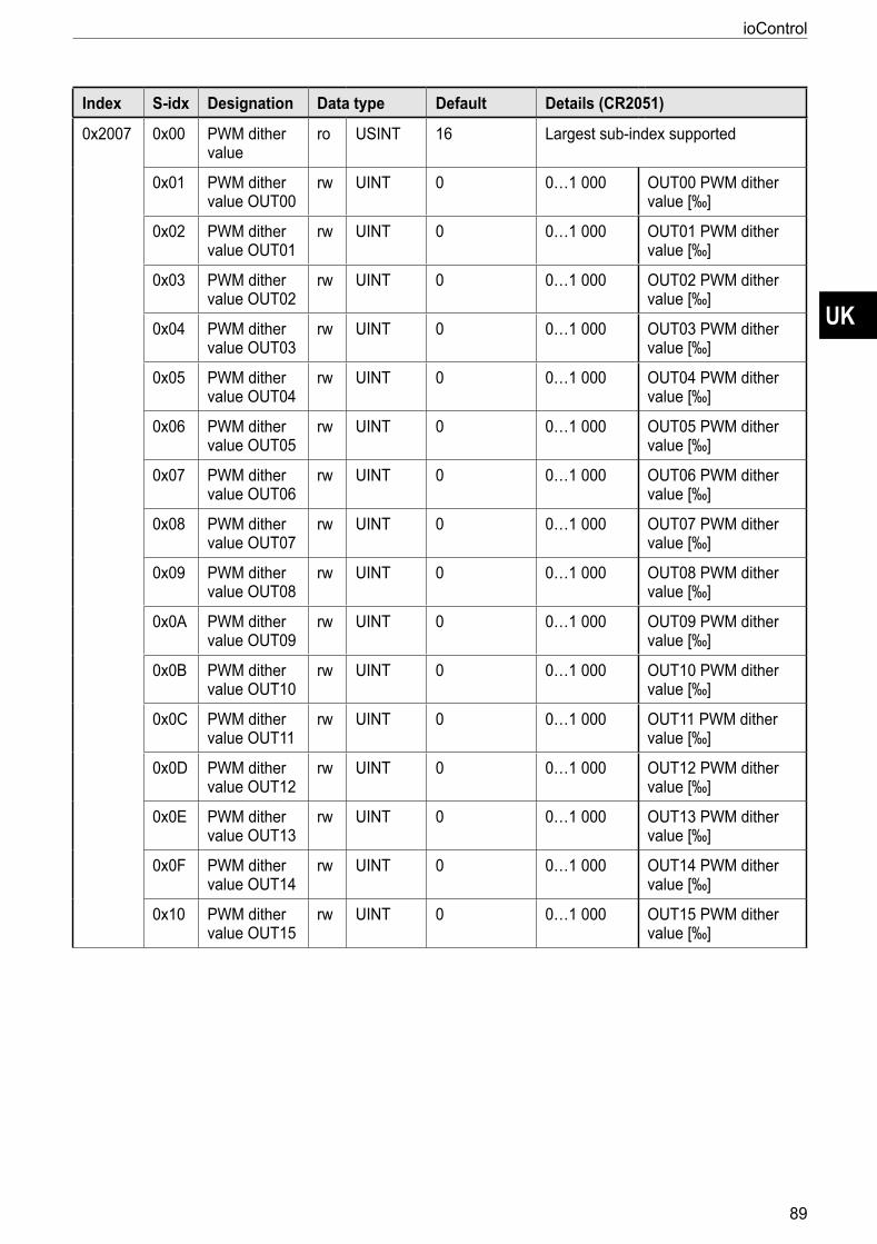
UK
ioControl
89
Index S-idx Designation Data type Default Details (CR2051)
0x2007 0x00 PWM dither value
ro USINT 16 Largest sub-index supported
0x01 PWM dither value OUT00
rw UINT 0 0…1 000 OUT00 PWM dither value [‰]
0x02 PWM dither value OUT01
rw UINT 0 0…1 000 OUT01 PWM dither value [‰]
0x03 PWM dither value OUT02
rw UINT 0 0…1 000 OUT02 PWM dither value [‰]
0x04 PWM dither value OUT03
rw UINT 0 0…1 000 OUT03 PWM dither value [‰]
0x05 PWM dither value OUT04
rw UINT 0 0…1 000 OUT04 PWM dither value [‰]
0x06 PWM dither value OUT05
rw UINT 0 0…1 000 OUT05 PWM dither value [‰]
0x07 PWM dither value OUT06
rw UINT 0 0…1 000 OUT06 PWM dither value [‰]
0x08 PWM dither value OUT07
rw UINT 0 0…1 000 OUT07 PWM dither value [‰]
0x09 PWM dither value OUT08
rw UINT 0 0…1 000 OUT08 PWM dither value [‰]
0x0A PWM dither value OUT09
rw UINT 0 0…1 000 OUT09 PWM dither value [‰]
0x0B PWM dither value OUT10
rw UINT 0 0…1 000 OUT10 PWM dither value [‰]
0x0C PWM dither value OUT11
rw UINT 0 0…1 000 OUT11 PWM dither value [‰]
0x0D PWM dither value OUT12
rw UINT 0 0…1 000 OUT12 PWM dither value [‰]
0x0E PWM dither value OUT13
rw UINT 0 0…1 000 OUT13 PWM dither value [‰]
0x0F PWM dither value OUT14
rw UINT 0 0…1 000 OUT14 PWM dither value [‰]
0x10 PWM dither value OUT15
rw UINT 0 0…1 000 OUT15 PWM dither value [‰]
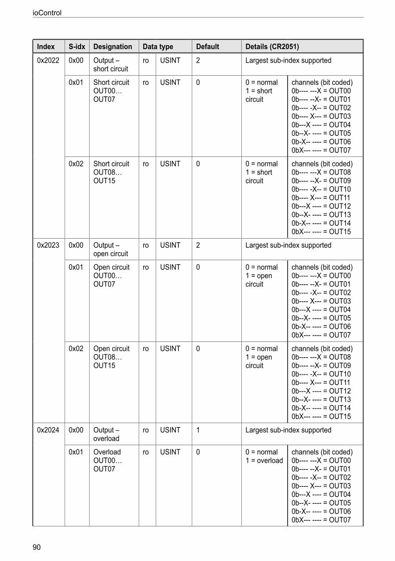
ioControl
90
Index S-idx Designation Data type Default Details (CR2051)
0x2022 0x00 Output – short circuit
ro USINT 2 Largest sub-index supported
0x01 Short circuit OUT00…OUT07
ro USINT 0 0 = normal 1 = short circuit
channels (bit coded) 0b---- ---X = OUT00 0b---- --X- = OUT01 0b---- -X-- = OUT02 0b---- X--- = OUT03 0b---X ---- = OUT04 0b--X- ---- = OUT05 0b-X-- ---- = OUT06 0bX--- ---- = OUT07
0x02 Short circuit OUT08…OUT15
ro USINT 0 0 = normal 1 = short circuit
channels (bit coded) 0b---- ---X = OUT08 0b---- --X- = OUT09 0b---- -X-- = OUT10 0b---- X--- = OUT11 0b---X ---- = OUT12 0b--X- ---- = OUT13 0b-X-- ---- = OUT14 0bX--- ---- = OUT15
0x2023 0x00 Output – open circuit
ro USINT 2 Largest sub-index supported
0x01 Open circuit OUT00…OUT07
ro USINT 0 0 = normal 1 = open circuit
channels (bit coded) 0b---- ---X = OUT00 0b---- --X- = OUT01 0b---- -X-- = OUT02 0b---- X--- = OUT03 0b---X ---- = OUT04 0b--X- ---- = OUT05 0b-X-- ---- = OUT06 0bX--- ---- = OUT07
0x02 Open circuit OUT08…OUT15
ro USINT 0 0 = normal 1 = open circuit
channels (bit coded) 0b---- ---X = OUT08 0b---- --X- = OUT09 0b---- -X-- = OUT10 0b---- X--- = OUT11 0b---X ---- = OUT12 0b--X- ---- = OUT13 0b-X-- ---- = OUT14 0bX--- ---- = OUT15
0x2024 0x00 Output – overload
ro USINT 1 Largest sub-index supported
0x01 Overload OUT00…OUT07
ro USINT 0 0 = normal 1 = overload
channels (bit coded) 0b---- ---X = OUT00 0b---- --X- = OUT01 0b---- -X-- = OUT02 0b---- X--- = OUT03 0b---X ---- = OUT04 0b--X- ---- = OUT05 0b-X-- ---- = OUT06 0bX--- ---- = OUT07
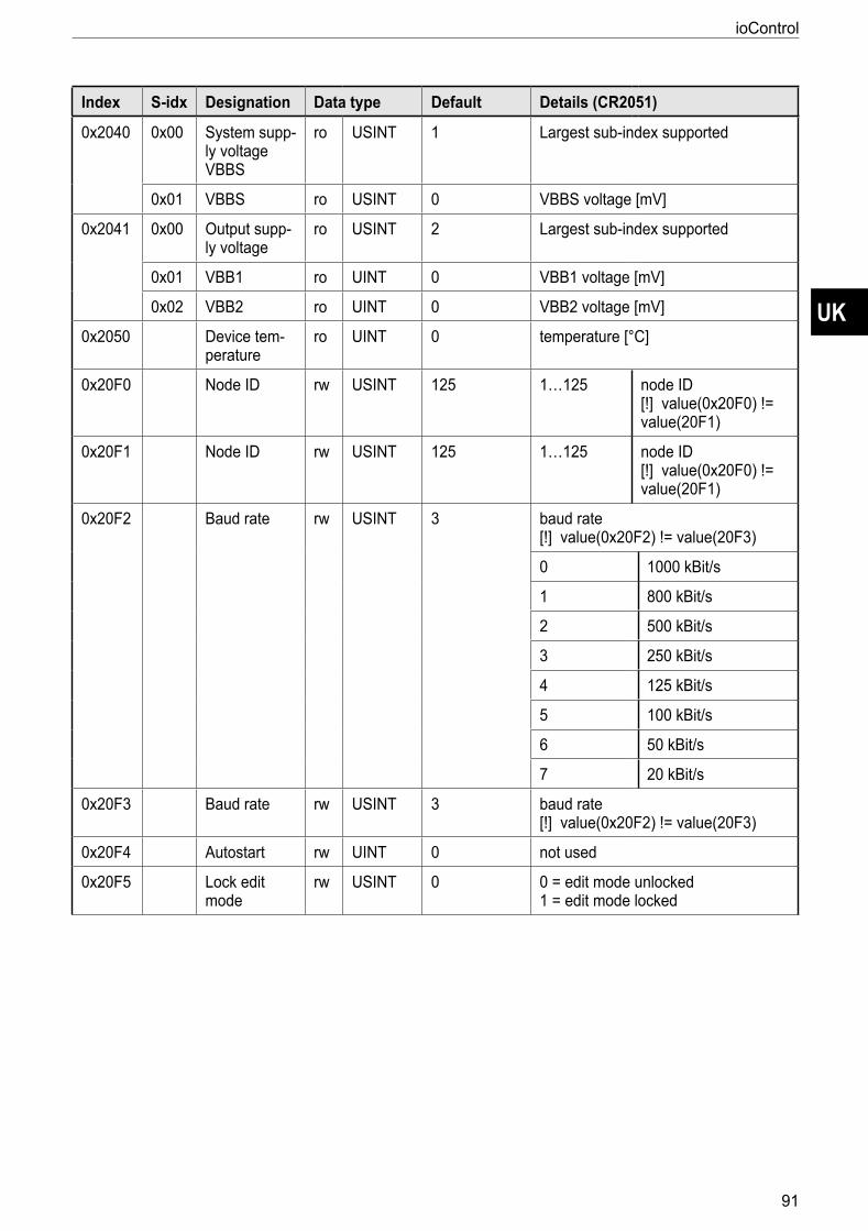
UK
ioControl
91
Index S-idx Designation Data type Default Details (CR2051)
0x2040 0x00 System supp-ly voltage VBBS
ro USINT 1 Largest sub-index supported
0x01 VBBS ro USINT 0 VBBS voltage [mV]
0x2041 0x00 Output supp-ly voltage
ro USINT 2 Largest sub-index supported
0x01 VBB1 ro UINT 0 VBB1 voltage [mV]
0x02 VBB2 ro UINT 0 VBB2 voltage [mV]
0x2050 Device tem-perature
ro UINT 0 temperature [°C]
0x20F0 Node ID rw USINT 125 1…125 node ID [!] value(0x20F0) != value(20F1)
0x20F1 Node ID rw USINT 125 1…125 node ID [!] value(0x20F0) != value(20F1)
0x20F2 Baud rate rw USINT 3 baud rate [!] value(0x20F2) != value(20F3)
0 1000 kBit/s
1 800 kBit/s
2 500 kBit/s
3 250 kBit/s
4 125 kBit/s
5 100 kBit/s
6 50 kBit/s
7 20 kBit/s
0x20F3 Baud rate rw USINT 3 baud rate [!] value(0x20F2) != value(20F3)
0x20F4 Autostart rw UINT 0 not used
0x20F5 Lock edit mode
rw USINT 0 0 = edit mode unlocked 1 = edit mode locked
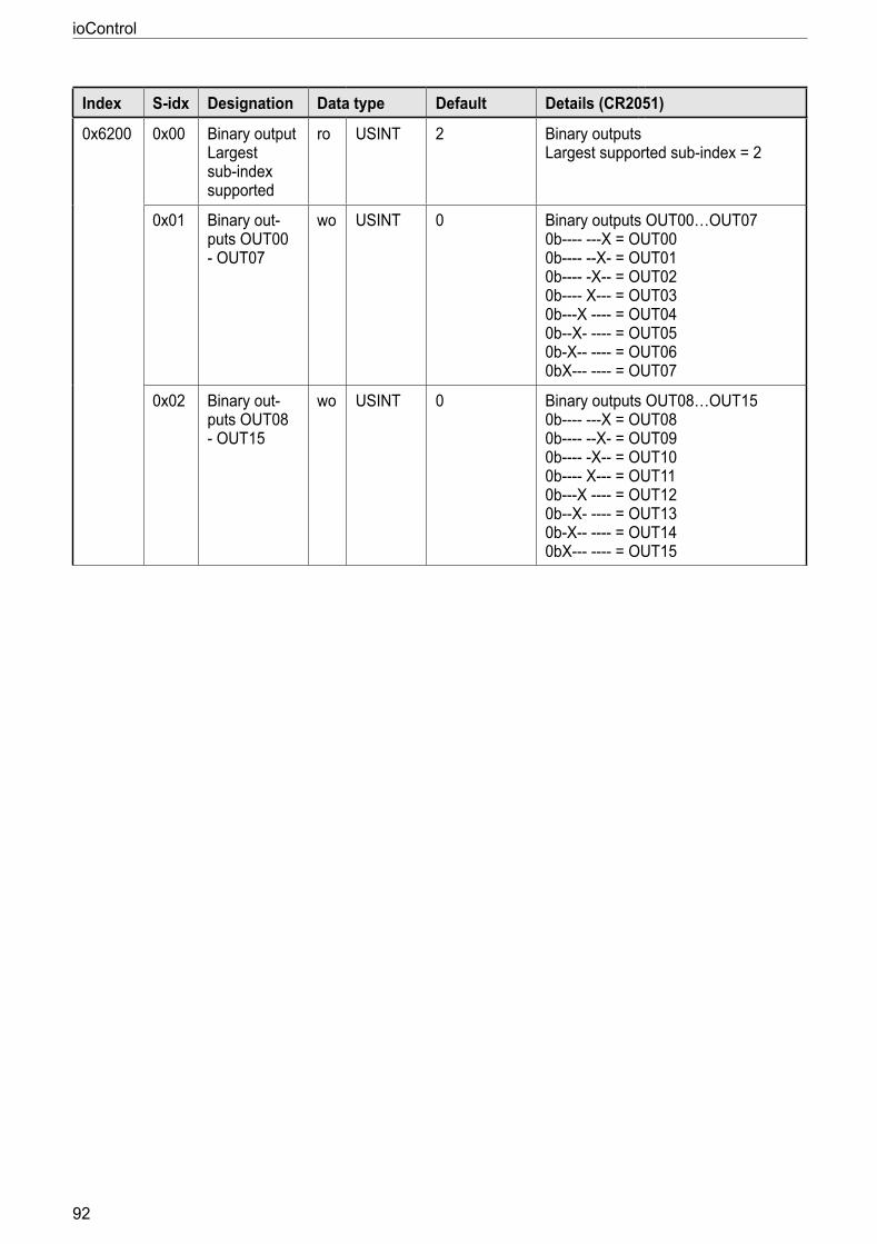
ioControl
92
Index S-idx Designation Data type Default Details (CR2051)
0x6200 0x00 Binary output Largest sub-index supported
ro USINT 2 Binary outputs Largest supported sub-index = 2
0x01 Binary out-puts OUT00 - OUT07
wo USINT 0 Binary outputs OUT00…OUT07 0b---- ---X = OUT00 0b---- --X- = OUT01 0b---- -X-- = OUT02 0b---- X--- = OUT03 0b---X ---- = OUT04 0b--X- ---- = OUT05 0b-X-- ---- = OUT06 0bX--- ---- = OUT07
0x02 Binary out-puts OUT08 - OUT15
wo USINT 0 Binary outputs OUT08…OUT15 0b---- ---X = OUT08 0b---- --X- = OUT09 0b---- -X-- = OUT10 0b---- X--- = OUT11 0b---X ---- = OUT12 0b--X- ---- = OUT13 0b-X-- ---- = OUT14 0bX--- ---- = OUT15
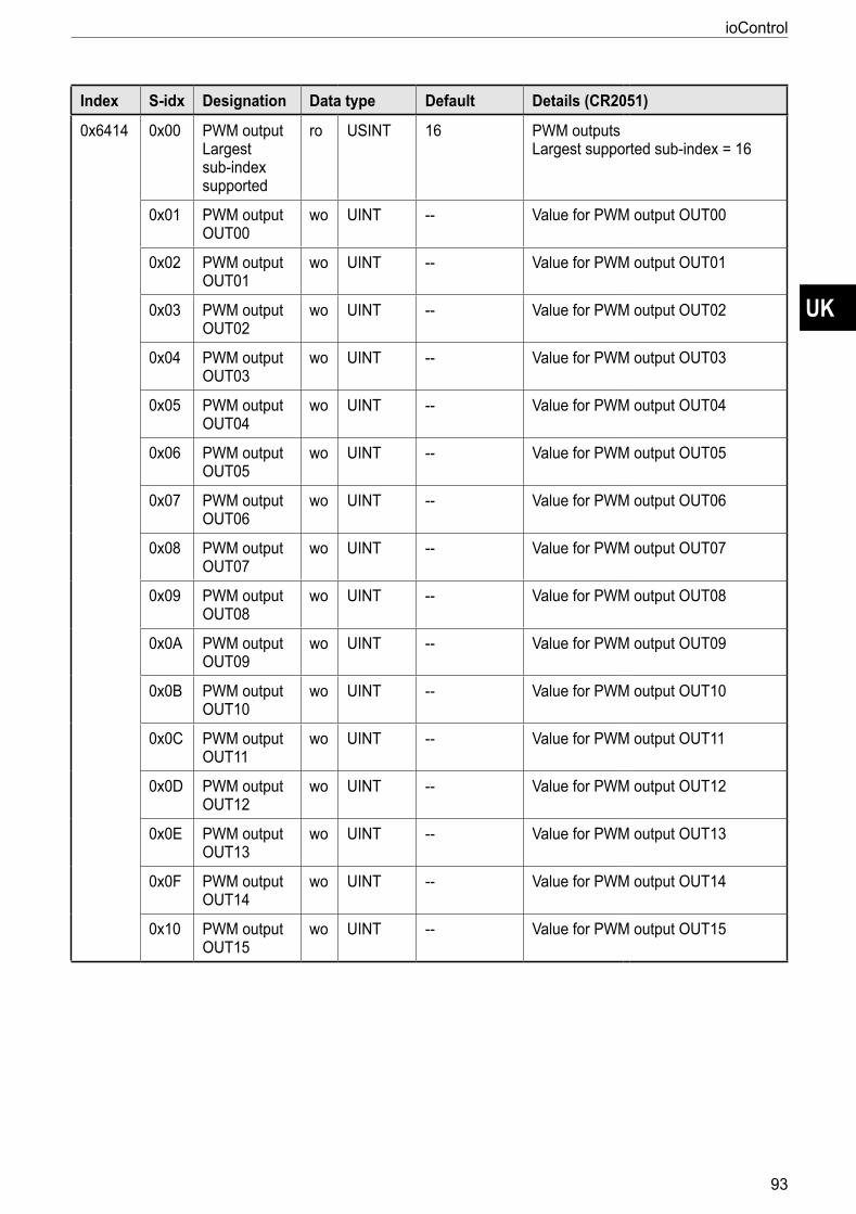
UK
ioControl
93
Index S-idx Designation Data type Default Details (CR2051)
0x6414 0x00 PWM output Largest sub-index supported
ro USINT 16 PWM outputs Largest supported sub-index = 16
0x01 PWM output OUT00
wo UINT -- Value for PWM output OUT00
0x02 PWM output OUT01
wo UINT -- Value for PWM output OUT01
0x03 PWM output OUT02
wo UINT -- Value for PWM output OUT02
0x04 PWM output OUT03
wo UINT -- Value for PWM output OUT03
0x05 PWM output OUT04
wo UINT -- Value for PWM output OUT04
0x06 PWM output OUT05
wo UINT -- Value for PWM output OUT05
0x07 PWM output OUT06
wo UINT -- Value for PWM output OUT06
0x08 PWM output OUT07
wo UINT -- Value for PWM output OUT07
0x09 PWM output OUT08
wo UINT -- Value for PWM output OUT08
0x0A PWM output OUT09
wo UINT -- Value for PWM output OUT09
0x0B PWM output OUT10
wo UINT -- Value for PWM output OUT10
0x0C PWM output OUT11
wo UINT -- Value for PWM output OUT11
0x0D PWM output OUT12
wo UINT -- Value for PWM output OUT12
0x0E PWM output OUT13
wo UINT -- Value for PWM output OUT13
0x0F PWM output OUT14
wo UINT -- Value for PWM output OUT14
0x10 PWM output OUT15
wo UINT -- Value for PWM output OUT15

ioControl
94
12.2.3 Device-specific CR2052Receive PDO communication parameters (index 0x1400…0x14FF):
Index S-idx Designation Data type Default Details (CR2052)
0x1400 0x00 Receive PDO Communica-tion Parame-ter Number of entries
ro USINT 0x02 Receive PDO 1: binary outputs 0 - 7number of entries = 2
0x01 COBID used by PDO
rw UDINT 0x200 + node ID
CAN ID of the first read PDO Bit 31 = 0 → PDO is valid Bit 31 = 1 → PDO is not valid
0x02 transmission type
rw USINT 0x01 0x00 = synch acyclic 0x010xF0 = synch cyclic; outputs are only updated after „n" synch objects n = 1…240 = 0x010xF0 0xFC/0xFD not implemented 0xFE = asynch man spec event; outputs are updated immediately 0xFF = asynch device profile event; outputs are updated immediately
0x1401 0x00 Receive PDO Communica-tion Parame-ter Number of entries
ro USINT 0x02 Receive PDO 2: PWM outputs 0 - 3 number of entries = 2
0x01 COBID used by PDO
rw UDINT 0x300 + node ID
CAN ID of the second read PDO Bit 31 = 0 → PDO is valid Bit 31 = 1 → PDO is not valid
0x02 transmission type
rw USINT 0x01 0x00 = synch acyclic 0x010xF0 = synch cyclic; outputs are only updated after „n" synch objects n = 1…240 = 0x010xF0 0xFC/0xFD not implemented 0xFE = asynch man spec event; outputs are updated immediately 0xFF = asynch device profile event; outputs are updated immediately
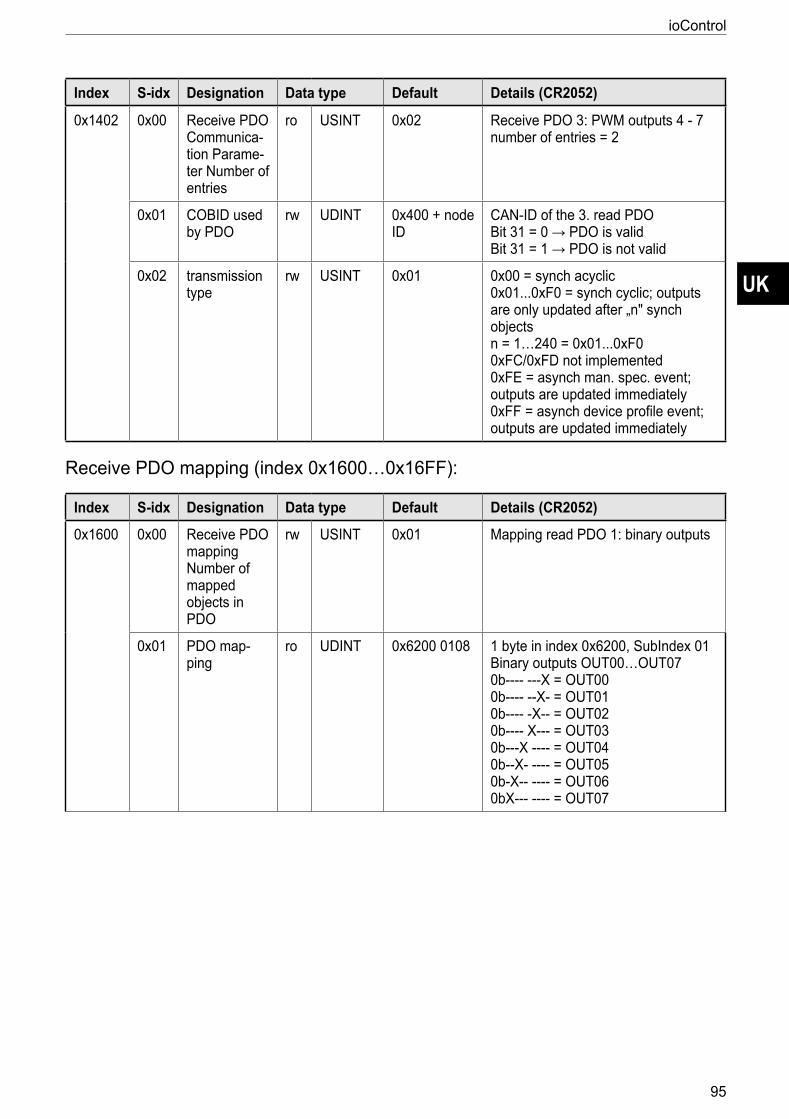
UK
ioControl
95
Index S-idx Designation Data type Default Details (CR2052)
0x1402 0x00 Receive PDO Communica-tion Parame-ter Number of entries
ro USINT 0x02 Receive PDO 3: PWM outputs 4 - 7 number of entries = 2
0x01 COBID used by PDO
rw UDINT 0x400 + node ID
CAN-ID of the 3 read PDO Bit 31 = 0 → PDO is valid Bit 31 = 1 → PDO is not valid
0x02 transmission type
rw USINT 0x01 0x00 = synch acyclic 0x010xF0 = synch cyclic; outputs are only updated after „n" synch objects n = 1…240 = 0x010xF0 0xFC/0xFD not implemented 0xFE = asynch man spec event; outputs are updated immediately 0xFF = asynch device profile event; outputs are updated immediately
Receive PDO mapping (index 0x1600…0x16FF):
Index S-idx Designation Data type Default Details (CR2052)
0x1600 0x00 Receive PDO mapping Number of mapped objects in PDO
rw USINT 0x01 Mapping read PDO 1: binary outputs
0x01 PDO map-ping
ro UDINT 0x6200 0108 1 byte in index 0x6200, SubIndex 01 Binary outputs OUT00…OUT07 0b---- ---X = OUT00 0b---- --X- = OUT01 0b---- -X-- = OUT02 0b---- X--- = OUT03 0b---X ---- = OUT04 0b--X- ---- = OUT05 0b-X-- ---- = OUT06 0bX--- ---- = OUT07
ioControl
96
Index S-idx Designation Data type Default Details (CR2052)
0x1601 0x00 Receive PDO mapping Number of mapped objects in PDO
rw USINT 0x04 Mapping read PDO 2: PWM outputs OUT00…OUT03 number of integrated application objects = 4
0x01 PDO map-ping
rw UDINT 0x6414 0110 PWM/current output OUT00 Index 0x6414, SubIndex 0x01 contains the preset value of the PWM output OUT00, the value is interpreted as duty cycle in ‰ or as target current value (depending on the configuration index 0x2000)
0x02 PDO map-ping
rw UDINT 0x6414 0210 PWM/ current output OUT01 Index 0x6414, SubIndex 0x02 contains the preset value of the PWM output OUT01, the value is interpreted as duty cycle in ‰ or as target current value (depending on the configuration index 0x2000)
0x03 PDO map-ping
rw UDINT 0x6414 0310 PWM/ current output OUT02 Index 0x6414, SubIndex 0x03 contains the preset value of the PWM output OUT02, the value is interpreted as duty cycle in ‰ or as target current value (depending on the configuration index 0x2000)
0x04 PDO map-ping
rw UDINT 0x6414 0410 PWM/ current output OUT03 Index 0x6414, SubIndex 0x04 contains the preset value of the PWM output OUT03, the value is interpreted as duty cycle in ‰ or as target current value (depending on the configuration index 0x2000)
UK
ioControl
97
Index S-idx Designation Data type Default Details (CR2052)
0x1602 0x00 Receive PDO mapping Number of mapped objects in PDO
rw USINT 0x04 Mapping read PDO 3: PWM outputs OUT04…OUT07 number of integrated application objects = 4
0x01 PDO map-ping
rw UDINT 0x6414 0510 PWM/ current output OUT04 Index 0x6414, SubIndex 0x05 contains the preset value of the PWM output OUT04, the value is interpreted as duty cycle in ‰ or as target current value (depending on the configuration index 0x2000)
0x02 PDO map-ping
rw UDINT 0x6414 0610 PWM/ current output OUT05 Index 0x6414, SubIndex 0x06 contains the preset value of the PWM output OUT05, the value is interpreted as duty cycle in ‰ or as target current value (depending on the configuration index 0x2000)
0x03 PDO map-ping
rw UDINT 0x6414 0710 PWM/ current output OUT06 Index 0x6414, SubIndex 0x07 contains the preset value of the PWM output OUT06, the value is interpreted as duty cycle in ‰ or as target current value (depending on the configuration index 0x2000)
0x04 PDO map-ping
rw UDINT 0x6414 0810 PWM/ current output OUT07 Index 0x6414, SubIndex 0x08 contains the preset value of the PWM output OUT07, the value is interpreted as duty cycle in ‰ or as target current value (depending on the configuration index 0x2000)
ioControl
98
Transmit PDO communication parameters (index 0x1800…0x18FF):
Index S-idx Designation Data type Default Details (CR2052)
0x1800 0x00 Transmit PDO Com-munication Parameter Number of entries
ro USINT 0x05 Configuration transmit PDO 1 number of entries = 5
0x01 COBID used by PDO
rw UDINT 0x180 + Node ID
CAN ID of the transmit PDO 1 Bit 31 = 0 → PDO is valid Bit 31 = 1 → PDO is not valid
0x02 transmission type
rw USINT 0x01 0x00 = synch acyclic 0x010xF0 = synch cyclic; values are only transmitted after „n" synch objects n = 1…240 = 0x010xF0 0xFC/0xFD not implemented 0xFE = asynch man spec event; values are immediately transferred 0xFF = asynch device profile event; values are immediately transferred
0x03 inhibit time rw UINT 0 delay time in the transmission type "asynch" before the PDO is transmitted again at the earliest (065535 • 100 µs)
0x04 reserved rw USINT 0 reserve
0x05 event time rw UINT 0 max transfer break in the transmissi-on type „asynch" (065535 ms) When this time has elapsed, the PDO is transferred even if the appl event has not accured

UK
ioControl
99
Index S-idx Designation Data type Default Details (CR2052)
0x1801 0x00 Transmit PDO Com-munication Parameter Number of entries
ro USINT 0x05 Configuration transmit PDO 2 number of entries = 5
0x01 COBID used by PDO
rw UDINT 0x280 + Node ID
CAN ID of the transmit PDO 2 Bit 31 = 0 → PDO is valid Bit 31 = 1 → PDO is not valid
0x02 transmission type
rw USINT 0x01 0x00 = synch acyclic 0x010xF0 = synch cyclic; values are only transmitted after „n" synch objects n = 1…240 = 0x010xF0 0xFC/0xFD not implemented 0xFE = asynch man spec event; values are immediately transferred 0xFF = asynch device profile event; values are immediately transferred
0x03 inhibit time rw UINT 0 delay time in the transmission type "asynch" before the PDO is transmitted again at the earliest (065535 • 100 µs)
0x04 reserved rw USINT 0 reserve
0x05 event time rw UINT 0 max transfer break in the transmissi-on type „asynch" (065535 ms) When this time has elapsed, the PDO is transferred even if the appl event has not accured

ioControl
100
Index S-idx Designation Data type Default Details (CR2052)
0x1802 0x00 Transmit PDO Com-munication Parameter Number of entries
ro USINT 0x05 Configuration transmit PDO 3 number of entries = 5
0x01 COBID used by PDO
rw UDINT 0x380 + Node ID
CAN ID of the transmit PDO 3 Bit 31 = 0 → PDO is valid Bit 31 = 1 → PDO is not valid
0x02 transmission type
rw USINT 0x01 0x00 = synch acyclic 0x010xF0 = synch cyclic; values are only transmitted after „n" synch objects n = 1…240 = 0x010xF0 0xFC/0xFD not implemented 0xFE = asynch man spec event; values are immediately transferred 0xFF = asynch device profile event; values are immediately transferred
0x03 inhibit time rw UINT 0 delay time in the transmission type "asynch" before the PDO is transmitted again at the earliest (065535 • 100 µs)
0x04 reserved rw USINT 0 reserve
0x05 event time rw UINT 0 max transfer break in the transmissi-on type „asynch" (065535 ms) When this time has elapsed, the PDO is transferred even if the appl event has not accured
UK
ioControl
101
Index S-idx Designation Data type Default Details (CR2052)
0x1803 0x00 Transmit PDO Com-munication Parameter Number of entries
ro USINT 0x05 Configuration transmit PDO 4 number of entries = 5
0x01 COBID used by PDO
rw UDINT 0x480 + Node ID
CAN ID of the transmit PDO 4 Bit 31 = 0 → PDO is valid Bit 31 = 1 → PDO is not valid
0x02 transmission type
rw USINT 0x01 0x00 = synch acyclic 0x010xF0 = synch cyclic; values are only transmitted after „n" synch objects n = 1…240 = 0x010xF0 0xFC/0xFD not implemented 0xFE = asynch man spec event; values are immediately transferred 0xFF = asynch device profile event; values are immediately transferred
0x03 inhibit time rw UINT 0 delay time in the transmission type "asynch" before the PDO is transmitted again at the earliest (065535 • 100 µs)
0x04 reserved rw USINT 0 reserve
0x05 event time rw UINT 0 max transfer break in the transmissi-on type „asynch" (065535 ms) When this time has elapsed, the PDO is transferred even if the appl event has not accured

ioControl
102
Index S-idx Designation Data type Default Details (CR2052)
0x1804 0x00 Transmit PDO Com-munication Parameter Number of entries
ro USINT 0x05 Configuration transmit PDO 5 number of entries = 5
0x01 COBID used by PDO
rw UDINT 0x181 + Node ID
CAN ID of the transmit PDO 5 Bit 31 = 0 → PDO is valid Bit 31 = 1 → PDO is not valid
0x02 transmission type
rw USINT 0x01 0x00 = synch acyclic 0x010xF0 = synch cyclic; values are only transmitted after „n" synch objects n = 1…240 = 0x010xF0 0xFC/0xFD not implemented 0xFE = asynch man spec event; values are immediately transferred 0xFF = asynch device profile event; values are immediately transferred
0x03 inhibit time rw UINT 0 delay time in the transmission type "asynch" before the PDO is transmitted again at the earliest (065535 • 100 µs)
0x04 reserved rw USINT 0 reserve
0x05 event time rw UINT 0 max transfer break in the transmissi-on type „asynch" (065535 ms) When this time has elapsed, the PDO is transferred even if the appl event has not accured

UK
ioControl
103
Index S-idx Designation Data type Default Details (CR2052)
0x1805 0x00 Transmit PDO Com-munication Parameter Number of entries
ro USINT 0x05 Configuration transmit PDO 6 number of entries = 5
0x01 COBID used by PDO
rw UDINT 0x281 + Node ID
CAN ID of the transmit PDO 6 Bit 31 = 0 → PDO is valid Bit 31 = 1 → PDO is not valid
0x02 transmission type
rw USINT 0x01 0x00 = synch acyclic 0x010xF0 = synch cyclic; values are only transmitted after „n" synch objects n = 1…240 = 0x010xF0 0xFC/0xFD not implemented 0xFE = asynch man spec event; values are immediately transferred 0xFF = asynch device profile event; values are immediately transferred
0x03 inhibit time rw UINT 0 delay time in the transmission type "asynch" before the PDO is transmitted again at the earliest (065535 • 100 µs)
0x04 reserved rw USINT 0 reserve
0x05 event time rw UINT 0 max transfer break in the transmissi-on type „asynch" (065535 ms) When this time has elapsed, the PDO is transferred even if the appl event has not accured

ioControl
104
Index S-idx Designation Data type Default Details (CR2052)
0x1806 0x00 Transmit PDO Com-munication Parameter Number of entries
ro USINT 0x05 Configuration transmit PDO 7 number of entries = 5
0x01 COBID used by PDO
rw UDINT 0x381 + Node ID
CAN ID of the transmit PDO 7 Bit 31 = 0 → PDO is valid Bit 31 = 1 → PDO is not valid
0x02 transmission type
rw USINT 0x01 0x00 = synch acyclic 0x010xF0 = synch cyclic; values are only transmitted after „n" synch objects n = 1…240 = 0x010xF0 0xFC/0xFD not implemented 0xFE = asynch man spec event; values are immediately transferred 0xFF = asynch device profile event; values are immediately transferred
0x03 inhibit time rw UINT 0 delay time in the transmission type "asynch" before the PDO is transmitted again at the earliest (065535 • 100 µs)
0x04 reserved rw USINT 0 reserve
0x05 event time rw UINT 0 max transfer break in the transmissi-on type „asynch" (065535 ms) When this time has elapsed, the PDO is transferred even if the appl event has not accured

UK
ioControl
105
Index S-idx Designation Data type Default Details (CR2052)
0x1807 0x00 Transmit PDO Com-munication Parameter Number of entries
ro USINT 0x05 Configuration transmit PDO 8 number of entries = 5
0x01 COBID used by PDO
rw UDINT 0x481 + Node ID
CAN ID of the transmit PDO 8 Bit 31 = 0 → PDO is valid Bit 31 = 1 → PDO is not valid
0x02 transmission type
rw USINT 0x01 0x00 = synch acyclic 0x010xF0 = synch cyclic; values are only transmitted after „n" synch objects n = 1…240 = 0x010xF0 0xFC/0xFD not implemented 0xFE = asynch man spec event; values are immediately transferred 0xFF = asynch device profile event; values are immediately transferred
0x03 inhibit time rw UINT 0 delay time in the transmission type "asynch" before the PDO is transmitted again at the earliest (065535 • 100 µs)
0x04 reserved rw USINT 0 reserve
0x05 event time rw UINT 0 max transfer break in the transmissi-on type „asynch" (065535 ms) When this time has elapsed, the PDO is transferred even if the appl event has not accured

ioControl
106
Index S-idx Designation Data type Default Details (CR2052)
0x1808 0x00 Transmit PDO Com-munication Parameter Number of entries
ro USINT 0x05 Configuration transmit PDO 9 number of entries = 5
0x01 COBID used by PDO
rw UDINT 0x182 + Node ID
CAN ID of the transmit PDO 9 Bit 31 = 0 → PDO is valid Bit 31 = 1 → PDO is not valid
0x02 transmission type
rw USINT 0x01 0x00 = synch acyclic 0x010xF0 = synch cyclic; values are only transmitted after „n" synch objects n = 1…240 = 0x010xF0 0xFC/0xFD not implemented 0xFE = asynch man spec event; values are immediately transferred 0xFF = asynch device profile event; values are immediately transferred
0x03 inhibit time rw UINT 0 delay time in the transmission type "asynch" before the PDO is transmitted again at the earliest (065535 • 100 µs)
0x04 reserved rw USINT 0 reserve
0x05 event time rw UINT 0 max transfer break in the transmissi-on type „asynch" (065535 ms) When this time has elapsed, the PDO is transferred even if the appl event has not accured
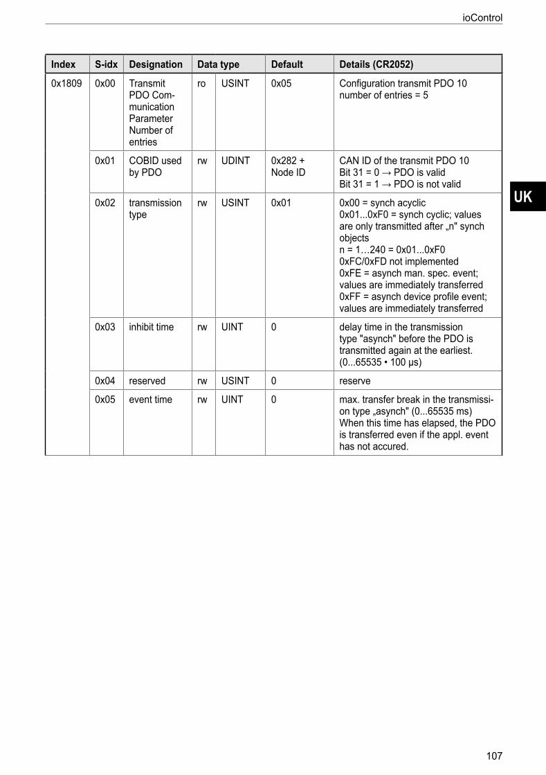
UK
ioControl
107
Index S-idx Designation Data type Default Details (CR2052)
0x1809 0x00 Transmit PDO Com-munication Parameter Number of entries
ro USINT 0x05 Configuration transmit PDO 10 number of entries = 5
0x01 COBID used by PDO
rw UDINT 0x282 + Node ID
CAN ID of the transmit PDO 10 Bit 31 = 0 → PDO is valid Bit 31 = 1 → PDO is not valid
0x02 transmission type
rw USINT 0x01 0x00 = synch acyclic 0x010xF0 = synch cyclic; values are only transmitted after „n" synch objects n = 1…240 = 0x010xF0 0xFC/0xFD not implemented 0xFE = asynch man spec event; values are immediately transferred 0xFF = asynch device profile event; values are immediately transferred
0x03 inhibit time rw UINT 0 delay time in the transmission type "asynch" before the PDO is transmitted again at the earliest (065535 • 100 µs)
0x04 reserved rw USINT 0 reserve
0x05 event time rw UINT 0 max transfer break in the transmissi-on type „asynch" (065535 ms) When this time has elapsed, the PDO is transferred even if the appl event has not accured
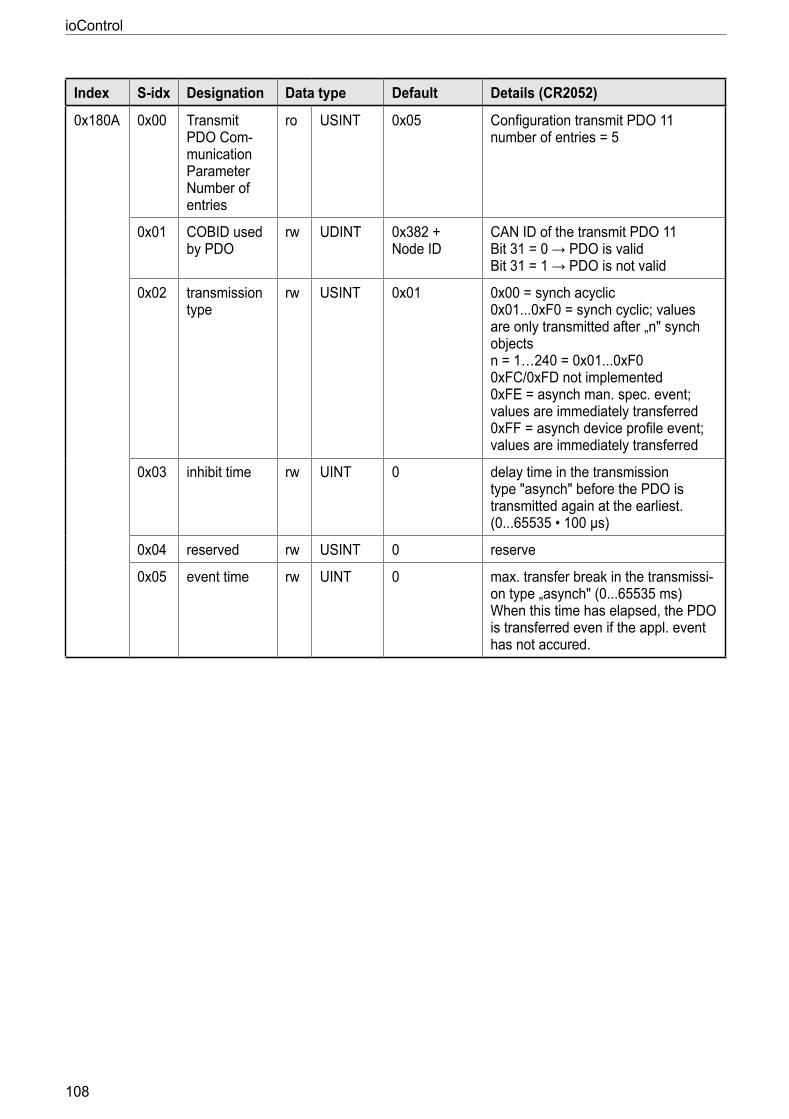
ioControl
108
Index S-idx Designation Data type Default Details (CR2052)
0x180A 0x00 Transmit PDO Com-munication Parameter Number of entries
ro USINT 0x05 Configuration transmit PDO 11 number of entries = 5
0x01 COBID used by PDO
rw UDINT 0x382 + Node ID
CAN ID of the transmit PDO 11 Bit 31 = 0 → PDO is valid Bit 31 = 1 → PDO is not valid
0x02 transmission type
rw USINT 0x01 0x00 = synch acyclic 0x010xF0 = synch cyclic; values are only transmitted after „n" synch objects n = 1…240 = 0x010xF0 0xFC/0xFD not implemented 0xFE = asynch man spec event; values are immediately transferred 0xFF = asynch device profile event; values are immediately transferred
0x03 inhibit time rw UINT 0 delay time in the transmission type "asynch" before the PDO is transmitted again at the earliest (065535 • 100 µs)
0x04 reserved rw USINT 0 reserve
0x05 event time rw UINT 0 max transfer break in the transmissi-on type „asynch" (065535 ms) When this time has elapsed, the PDO is transferred even if the appl event has not accured
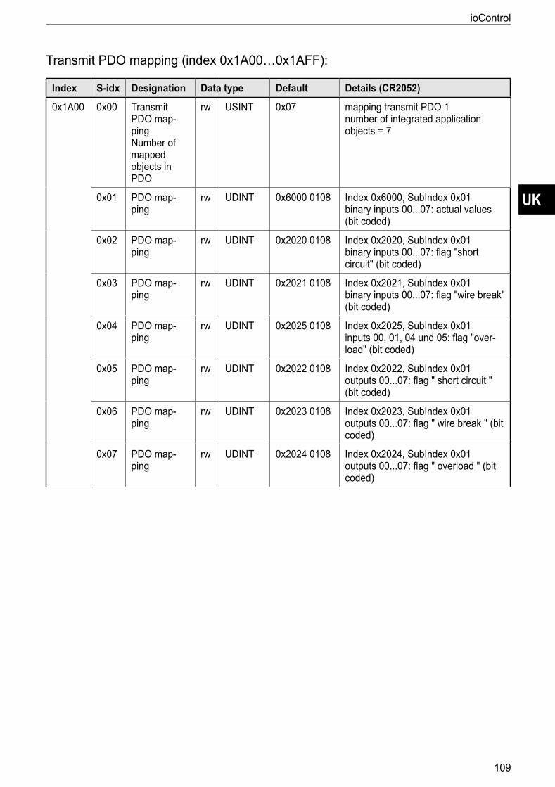
UK
ioControl
109
Transmit PDO mapping (index 0x1A00…0x1AFF):
Index S-idx Designation Data type Default Details (CR2052)
0x1A00 0x00 Transmit PDO map-ping Number of mapped objects in PDO
rw USINT 0x07 mapping transmit PDO 1 number of integrated application objects = 7
0x01 PDO map-ping
rw UDINT 0x6000 0108 Index 0x6000, SubIndex 0x01 binary inputs 0007: actual values (bit coded)
0x02 PDO map-ping
rw UDINT 0x2020 0108 Index 0x2020, SubIndex 0x01 binary inputs 0007: flag "short circuit" (bit coded)
0x03 PDO map-ping
rw UDINT 0x2021 0108 Index 0x2021, SubIndex 0x01 binary inputs 0007: flag "wire break" (bit coded)
0x04 PDO map-ping
rw UDINT 0x2025 0108 Index 0x2025, SubIndex 0x01 inputs 00, 01, 04 und 05: flag "over-load" (bit coded)
0x05 PDO map-ping
rw UDINT 0x2022 0108 Index 0x2022, SubIndex 0x01 outputs 0007: flag " short circuit " (bit coded)
0x06 PDO map-ping
rw UDINT 0x2023 0108 Index 0x2023, SubIndex 0x01 outputs 0007: flag " wire break " (bit coded)
0x07 PDO map-ping
rw UDINT 0x2024 0108 Index 0x2024, SubIndex 0x01 outputs 0007: flag " overload " (bit coded)
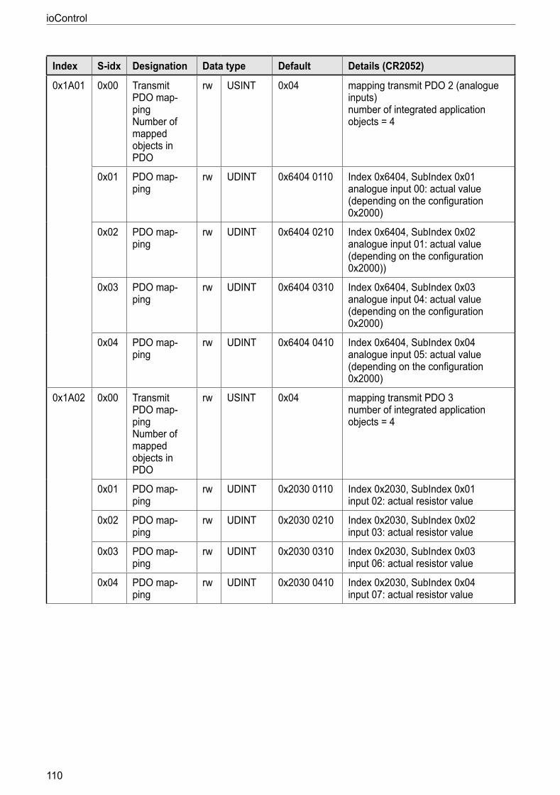
ioControl
110
Index S-idx Designation Data type Default Details (CR2052)
0x1A01 0x00 Transmit PDO map-ping Number of mapped objects in PDO
rw USINT 0x04 mapping transmit PDO 2 (analogue inputs) number of integrated application objects = 4
0x01 PDO map-ping
rw UDINT 0x6404 0110 Index 0x6404, SubIndex 0x01 analogue input 00: actual value (depending on the configuration 0x2000)
0x02 PDO map-ping
rw UDINT 0x6404 0210 Index 0x6404, SubIndex 0x02 analogue input 01: actual value (depending on the configuration 0x2000))
0x03 PDO map-ping
rw UDINT 0x6404 0310 Index 0x6404, SubIndex 0x03 analogue input 04: actual value (depending on the configuration 0x2000)
0x04 PDO map-ping
rw UDINT 0x6404 0410 Index 0x6404, SubIndex 0x04 analogue input 05: actual value (depending on the configuration 0x2000)
0x1A02 0x00 Transmit PDO map-ping Number of mapped objects in PDO
rw USINT 0x04 mapping transmit PDO 3 number of integrated application objects = 4
0x01 PDO map-ping
rw UDINT 0x2030 0110 Index 0x2030, SubIndex 0x01 input 02: actual resistor value
0x02 PDO map-ping
rw UDINT 0x2030 0210 Index 0x2030, SubIndex 0x02 input 03: actual resistor value
0x03 PDO map-ping
rw UDINT 0x2030 0310 Index 0x2030, SubIndex 0x03 input 06: actual resistor value
0x04 PDO map-ping
rw UDINT 0x2030 0410 Index 0x2030, SubIndex 0x04 input 07: actual resistor value
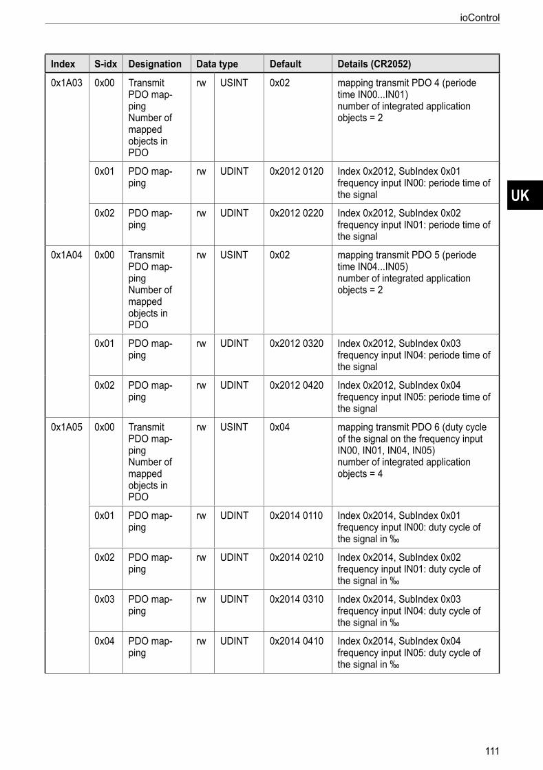
UK
ioControl
111
Index S-idx Designation Data type Default Details (CR2052)
0x1A03 0x00 Transmit PDO map-ping Number of mapped objects in PDO
rw USINT 0x02 mapping transmit PDO 4 (periode time IN00IN01) number of integrated application objects = 2
0x01 PDO map-ping
rw UDINT 0x2012 0120 Index 0x2012, SubIndex 0x01 frequency input IN00: periode time of the signal
0x02 PDO map-ping
rw UDINT 0x2012 0220 Index 0x2012, SubIndex 0x02 frequency input IN01: periode time of the signal
0x1A04 0x00 Transmit PDO map-ping Number of mapped objects in PDO
rw USINT 0x02 mapping transmit PDO 5 (periode time IN04IN05) number of integrated application objects = 2
0x01 PDO map-ping
rw UDINT 0x2012 0320 Index 0x2012, SubIndex 0x03 frequency input IN04: periode time of the signal
0x02 PDO map-ping
rw UDINT 0x2012 0420 Index 0x2012, SubIndex 0x04 frequency input IN05: periode time of the signal
0x1A05 0x00 Transmit PDO map-ping Number of mapped objects in PDO
rw USINT 0x04 mapping transmit PDO 6 (duty cycle of the signal on the frequency input IN00, IN01, IN04, IN05) number of integrated application objects = 4
0x01 PDO map-ping
rw UDINT 0x2014 0110 Index 0x2014, SubIndex 0x01 frequency input IN00: duty cycle of the signal in ‰
0x02 PDO map-ping
rw UDINT 0x2014 0210 Index 0x2014, SubIndex 0x02 frequency input IN01: duty cycle of the signal in ‰
0x03 PDO map-ping
rw UDINT 0x2014 0310 Index 0x2014, SubIndex 0x03 frequency input IN04: duty cycle of the signal in ‰
0x04 PDO map-ping
rw UDINT 0x2014 0410 Index 0x2014, SubIndex 0x04 frequency input IN05: duty cycle of the signal in ‰
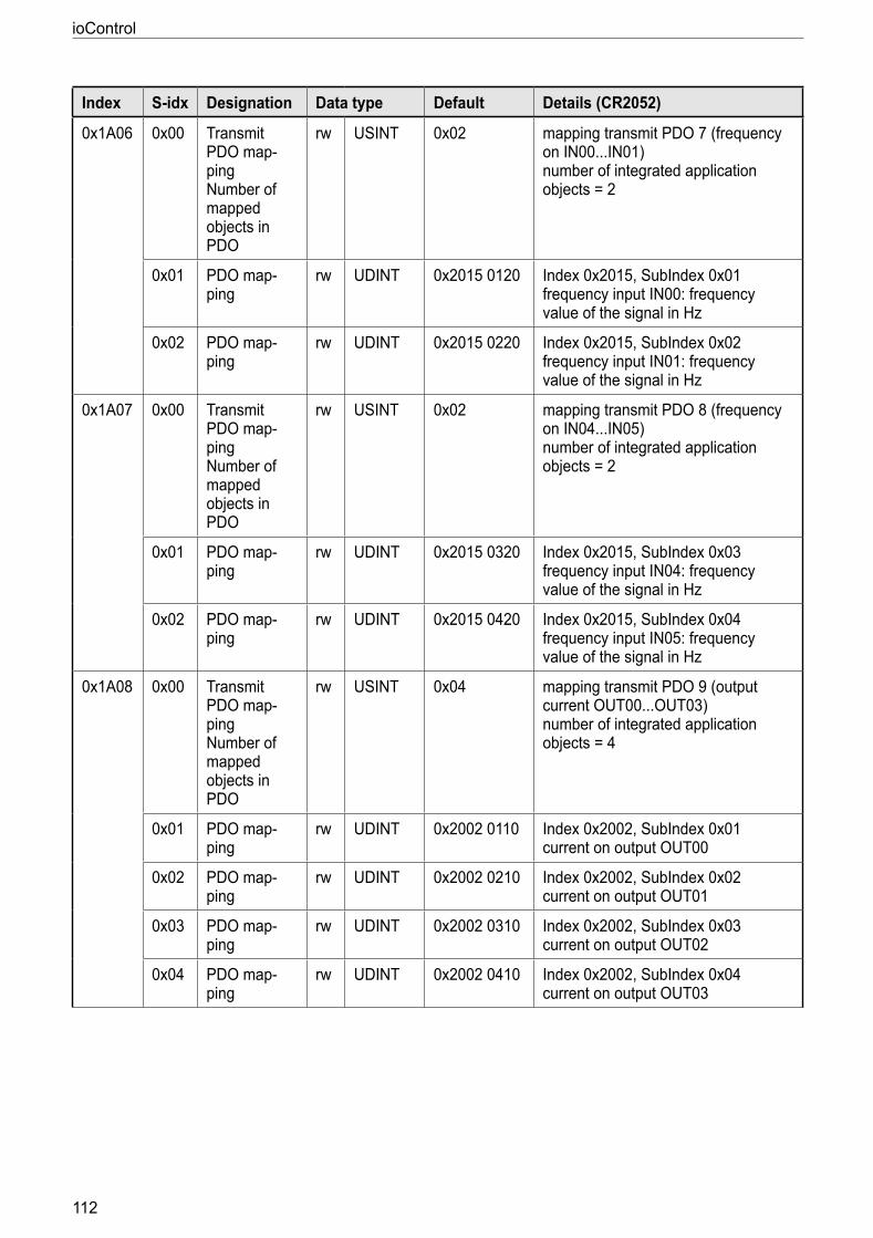
ioControl
112
Index S-idx Designation Data type Default Details (CR2052)
0x1A06 0x00 Transmit PDO map-ping Number of mapped objects in PDO
rw USINT 0x02 mapping transmit PDO 7 (frequency on IN00IN01) number of integrated application objects = 2
0x01 PDO map-ping
rw UDINT 0x2015 0120 Index 0x2015, SubIndex 0x01 frequency input IN00: frequency value of the signal in Hz
0x02 PDO map-ping
rw UDINT 0x2015 0220 Index 0x2015, SubIndex 0x02 frequency input IN01: frequency value of the signal in Hz
0x1A07 0x00 Transmit PDO map-ping Number of mapped objects in PDO
rw USINT 0x02 mapping transmit PDO 8 (frequency on IN04IN05) number of integrated application objects = 2
0x01 PDO map-ping
rw UDINT 0x2015 0320 Index 0x2015, SubIndex 0x03 frequency input IN04: frequency value of the signal in Hz
0x02 PDO map-ping
rw UDINT 0x2015 0420 Index 0x2015, SubIndex 0x04 frequency input IN05: frequency value of the signal in Hz
0x1A08 0x00 Transmit PDO map-ping Number of mapped objects in PDO
rw USINT 0x04 mapping transmit PDO 9 (output current OUT00OUT03) number of integrated application objects = 4
0x01 PDO map-ping
rw UDINT 0x2002 0110 Index 0x2002, SubIndex 0x01 current on output OUT00
0x02 PDO map-ping
rw UDINT 0x2002 0210 Index 0x2002, SubIndex 0x02 current on output OUT01
0x03 PDO map-ping
rw UDINT 0x2002 0310 Index 0x2002, SubIndex 0x03 current on output OUT02
0x04 PDO map-ping
rw UDINT 0x2002 0410 Index 0x2002, SubIndex 0x04 current on output OUT03
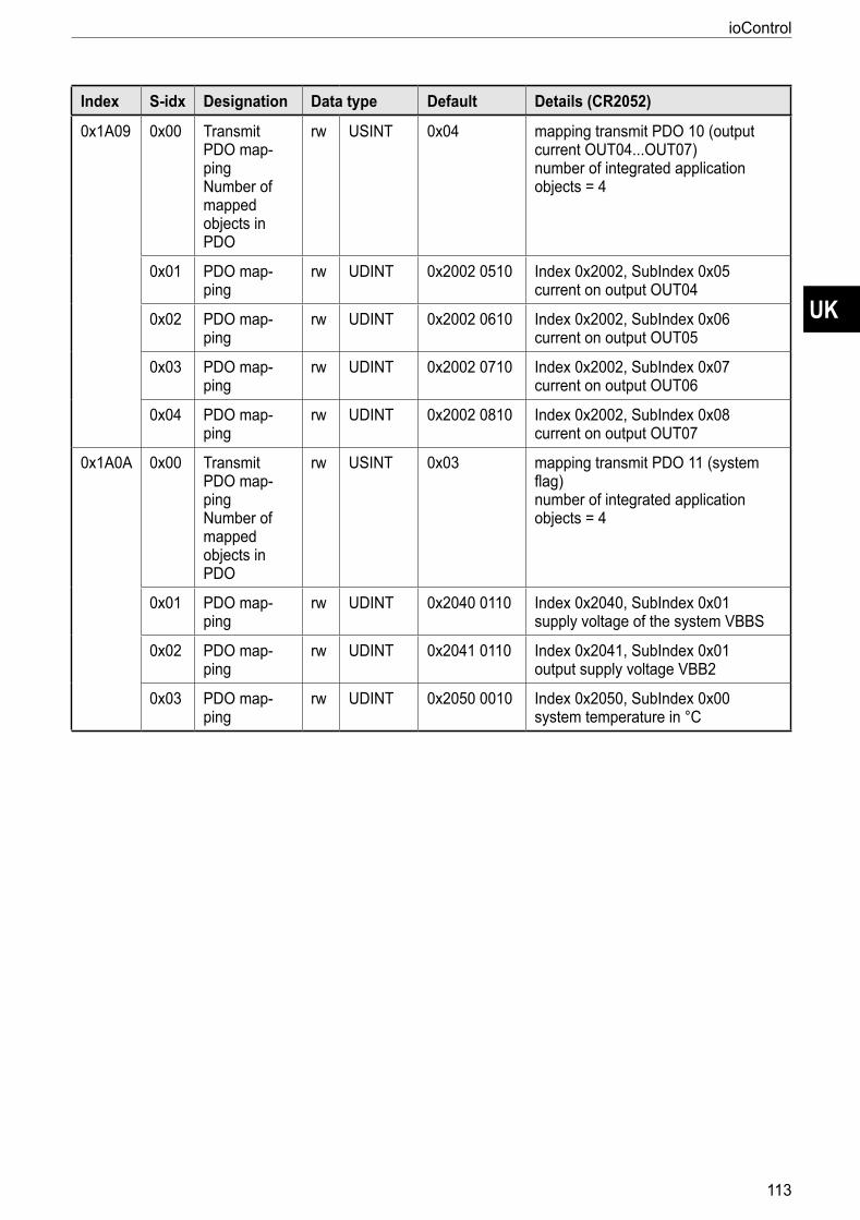
UK
ioControl
113
Index S-idx Designation Data type Default Details (CR2052)
0x1A09 0x00 Transmit PDO map-ping Number of mapped objects in PDO
rw USINT 0x04 mapping transmit PDO 10 (output current OUT04OUT07) number of integrated application objects = 4
0x01 PDO map-ping
rw UDINT 0x2002 0510 Index 0x2002, SubIndex 0x05 current on output OUT04
0x02 PDO map-ping
rw UDINT 0x2002 0610 Index 0x2002, SubIndex 0x06 current on output OUT05
0x03 PDO map-ping
rw UDINT 0x2002 0710 Index 0x2002, SubIndex 0x07 current on output OUT06
0x04 PDO map-ping
rw UDINT 0x2002 0810 Index 0x2002, SubIndex 0x08 current on output OUT07
0x1A0A 0x00 Transmit PDO map-ping Number of mapped objects in PDO
rw USINT 0x03 mapping transmit PDO 11 (system flag) number of integrated application objects = 4
0x01 PDO map-ping
rw UDINT 0x2040 0110 Index 0x2040, SubIndex 0x01 supply voltage of the system VBBS
0x02 PDO map-ping
rw UDINT 0x2041 0110 Index 0x2041, SubIndex 0x01 output supply voltage VBB2
0x03 PDO map-ping
rw UDINT 0x2050 0010 Index 0x2050, SubIndex 0x00 system temperature in °C
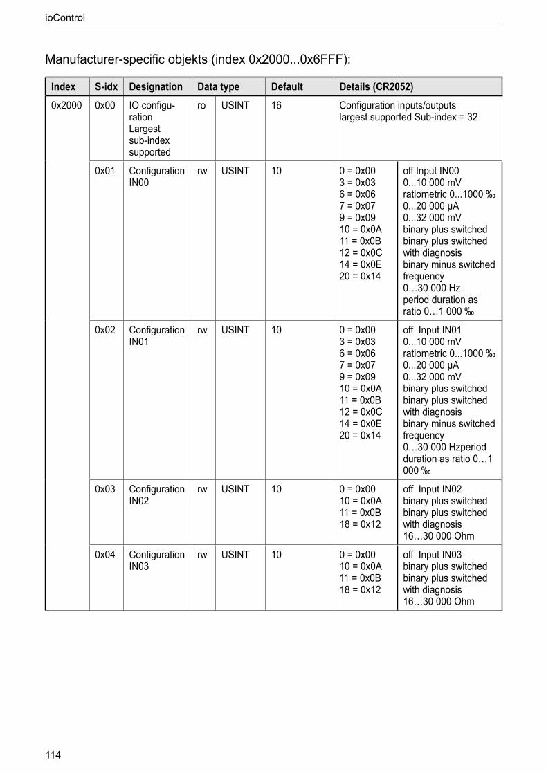
ioControl
114
Manufacturer-specific objekts (index 0x20000x6FFF):
Index S-idx Designation Data type Default Details (CR2052)
0x2000 0x00 IO configu-ration Largest sub-index supported
ro USINT 16 Configuration inputs/outputs largest supported Sub-index = 32
0x01 Configuration IN00
rw USINT 10 0 = 0x00 3 = 0x03 6 = 0x06 7 = 0x07 9 = 0x09 10 = 0x0A 11 = 0x0B 12 = 0x0C 14 = 0x0E 20 = 0x14
off Input IN00 010 000 mV ratiometric 01000 ‰ 020 000 µA 032 000 mV binary plus switched binary plus switched with diagnosis binary minus switched frequency 0…30 000 Hz period duration as ratio 0…1 000 ‰
0x02 Configuration IN01
rw USINT 10 0 = 0x00 3 = 0x03 6 = 0x06 7 = 0x07 9 = 0x09 10 = 0x0A 11 = 0x0B 12 = 0x0C 14 = 0x0E 20 = 0x14
off Input IN01 010 000 mV ratiometric 01000 ‰ 020 000 µA 032 000 mV binary plus switched binary plus switched with diagnosis binary minus switched frequency 0…30 000 Hzperiod duration as ratio 0…1 000 ‰
0x03 Configuration IN02
rw USINT 10 0 = 0x00 10 = 0x0A 11 = 0x0B 18 = 0x12
off Input IN02 binary plus switched binary plus switched with diagnosis 16…30 000 Ohm
0x04 Configuration IN03
rw USINT 10 0 = 0x00 10 = 0x0A 11 = 0x0B 18 = 0x12
off Input IN03 binary plus switched binary plus switched with diagnosis 16…30 000 Ohm
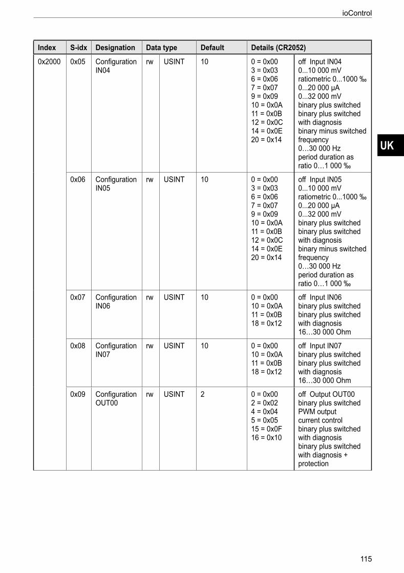
UK
ioControl
115
Index S-idx Designation Data type Default Details (CR2052)
0x2000 0x05 Configuration IN04
rw USINT 10 0 = 0x00 3 = 0x03 6 = 0x06 7 = 0x07 9 = 0x09 10 = 0x0A 11 = 0x0B 12 = 0x0C 14 = 0x0E 20 = 0x14
off Input IN04 010 000 mV ratiometric 01000 ‰ 020 000 µA 032 000 mV binary plus switched binary plus switched with diagnosis binary minus switched frequency 0…30 000 Hz period duration as ratio 0…1 000 ‰
0x06 Configuration IN05
rw USINT 10 0 = 0x00 3 = 0x03 6 = 0x06 7 = 0x07 9 = 0x09 10 = 0x0A 11 = 0x0B 12 = 0x0C 14 = 0x0E 20 = 0x14
off Input IN05 010 000 mV ratiometric 01000 ‰ 020 000 µA 032 000 mV binary plus switched binary plus switched with diagnosis binary minus switched frequency 0…30 000 Hz period duration as ratio 0…1 000 ‰
0x07 Configuration IN06
rw USINT 10 0 = 0x00 10 = 0x0A 11 = 0x0B 18 = 0x12
off Input IN06 binary plus switched binary plus switched with diagnosis 16…30 000 Ohm
0x08 Configuration IN07
rw USINT 10 0 = 0x00 10 = 0x0A 11 = 0x0B 18 = 0x12
off Input IN07 binary plus switched binary plus switched with diagnosis 16…30 000 Ohm
0x09 Configuration OUT00
rw USINT 2 0 = 0x00 2 = 0x02 4 = 0x04 5 = 0x05 15 = 0x0F 16 = 0x10
off Output OUT00 binary plus switched PWM output current control binary plus switched with diagnosis binary plus switched with diagnosis + protection
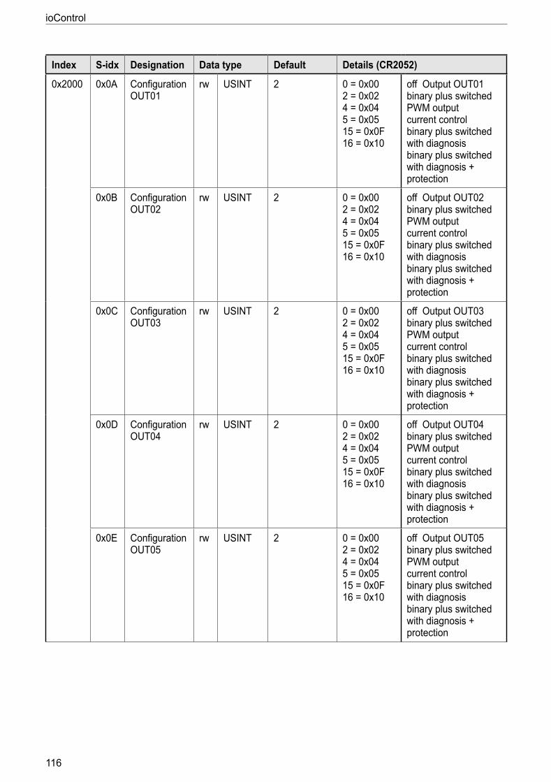
ioControl
116
Index S-idx Designation Data type Default Details (CR2052)
0x2000 0x0A Configuration OUT01
rw USINT 2 0 = 0x00 2 = 0x02 4 = 0x04 5 = 0x05 15 = 0x0F 16 = 0x10
off Output OUT01 binary plus switched PWM output current control binary plus switched with diagnosis binary plus switched with diagnosis + protection
0x0B Configuration OUT02
rw USINT 2 0 = 0x00 2 = 0x02 4 = 0x04 5 = 0x05 15 = 0x0F 16 = 0x10
off Output OUT02 binary plus switched PWM output current control binary plus switched with diagnosis binary plus switched with diagnosis + protection
0x0C Configuration OUT03
rw USINT 2 0 = 0x00 2 = 0x02 4 = 0x04 5 = 0x05 15 = 0x0F 16 = 0x10
off Output OUT03 binary plus switched PWM output current control binary plus switched with diagnosis binary plus switched with diagnosis + protection
0x0D Configuration OUT04
rw USINT 2 0 = 0x00 2 = 0x02 4 = 0x04 5 = 0x05 15 = 0x0F 16 = 0x10
off Output OUT04 binary plus switched PWM output current control binary plus switched with diagnosis binary plus switched with diagnosis + protection
0x0E Configuration OUT05
rw USINT 2 0 = 0x00 2 = 0x02 4 = 0x04 5 = 0x05 15 = 0x0F 16 = 0x10
off Output OUT05 binary plus switched PWM output current control binary plus switched with diagnosis binary plus switched with diagnosis + protection
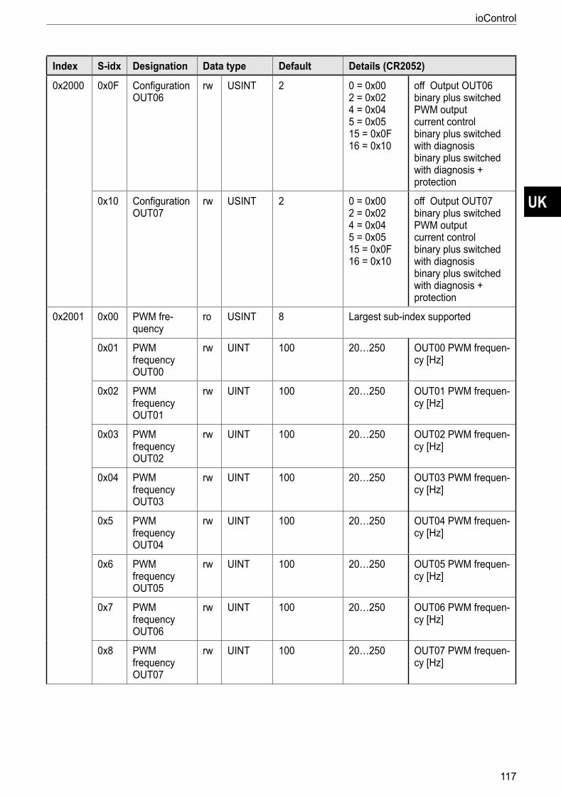
UK
ioControl
117
Index S-idx Designation Data type Default Details (CR2052)
0x2000 0x0F Configuration OUT06
rw USINT 2 0 = 0x00 2 = 0x02 4 = 0x04 5 = 0x05 15 = 0x0F 16 = 0x10
off Output OUT06 binary plus switched PWM output current control binary plus switched with diagnosis binary plus switched with diagnosis + protection
0x10 Configuration OUT07
rw USINT 2 0 = 0x00 2 = 0x02 4 = 0x04 5 = 0x05 15 = 0x0F 16 = 0x10
off Output OUT07 binary plus switched PWM output current control binary plus switched with diagnosis binary plus switched with diagnosis + protection
0x2001 0x00 PWM fre-quency
ro USINT 8 Largest sub-index supported
0x01 PWM frequency OUT00
rw UINT 100 20…250 OUT00 PWM frequen-cy [Hz]
0x02 PWM frequency OUT01
rw UINT 100 20…250 OUT01 PWM frequen-cy [Hz]
0x03 PWM frequency OUT02
rw UINT 100 20…250 OUT02 PWM frequen-cy [Hz]
0x04 PWM frequency OUT03
rw UINT 100 20…250 OUT03 PWM frequen-cy [Hz]
0x5 PWM frequency OUT04
rw UINT 100 20…250 OUT04 PWM frequen-cy [Hz]
0x6 PWM frequency OUT05
rw UINT 100 20…250 OUT05 PWM frequen-cy [Hz]
0x7 PWM frequency OUT06
rw UINT 100 20…250 OUT06 PWM frequen-cy [Hz]
0x8 PWM frequency OUT07
rw UINT 100 20…250 OUT07 PWM frequen-cy [Hz]
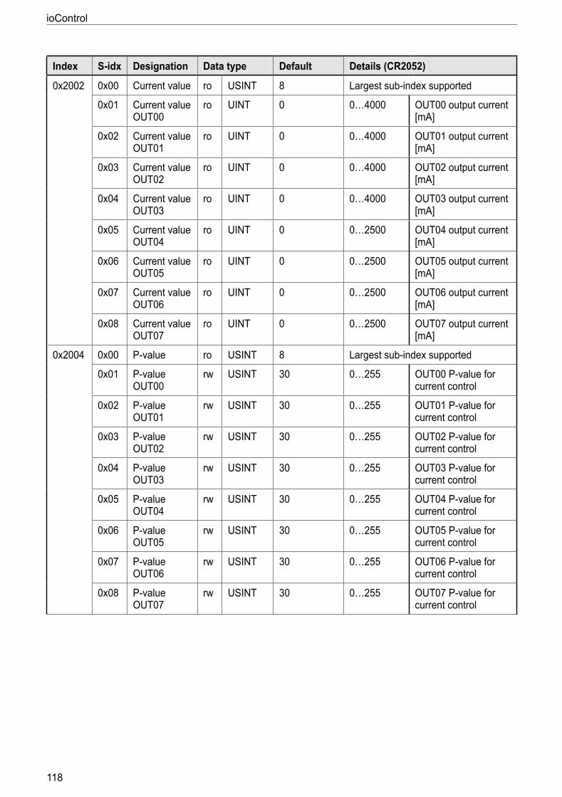
ioControl
118
Index S-idx Designation Data type Default Details (CR2052)
0x2002 0x00 Current value ro USINT 8 Largest sub-index supported
0x01 Current value OUT00
ro UINT 0 0…4000 OUT00 output current [mA]
0x02 Current value OUT01
ro UINT 0 0…4000 OUT01 output current [mA]
0x03 Current value OUT02
ro UINT 0 0…4000 OUT02 output current [mA]
0x04 Current value OUT03
ro UINT 0 0…4000 OUT03 output current [mA]
0x05 Current value OUT04
ro UINT 0 0…2500 OUT04 output current [mA]
0x06 Current value OUT05
ro UINT 0 0…2500 OUT05 output current [mA]
0x07 Current value OUT06
ro UINT 0 0…2500 OUT06 output current [mA]
0x08 Current value OUT07
ro UINT 0 0…2500 OUT07 output current [mA]
0x2004 0x00 P-value ro USINT 8 Largest sub-index supported
0x01 P-value OUT00
rw USINT 30 0…255 OUT00 P-value for current control
0x02 P-value OUT01
rw USINT 30 0…255 OUT01 P-value for current control
0x03 P-value OUT02
rw USINT 30 0…255 OUT02 P-value for current control
0x04 P-value OUT03
rw USINT 30 0…255 OUT03 P-value for current control
0x05 P-value OUT04
rw USINT 30 0…255 OUT04 P-value for current control
0x06 P-value OUT05
rw USINT 30 0…255 OUT05 P-value for current control
0x07 P-value OUT06
rw USINT 30 0…255 OUT06 P-value for current control
0x08 P-value OUT07
rw USINT 30 0…255 OUT07 P-value for current control
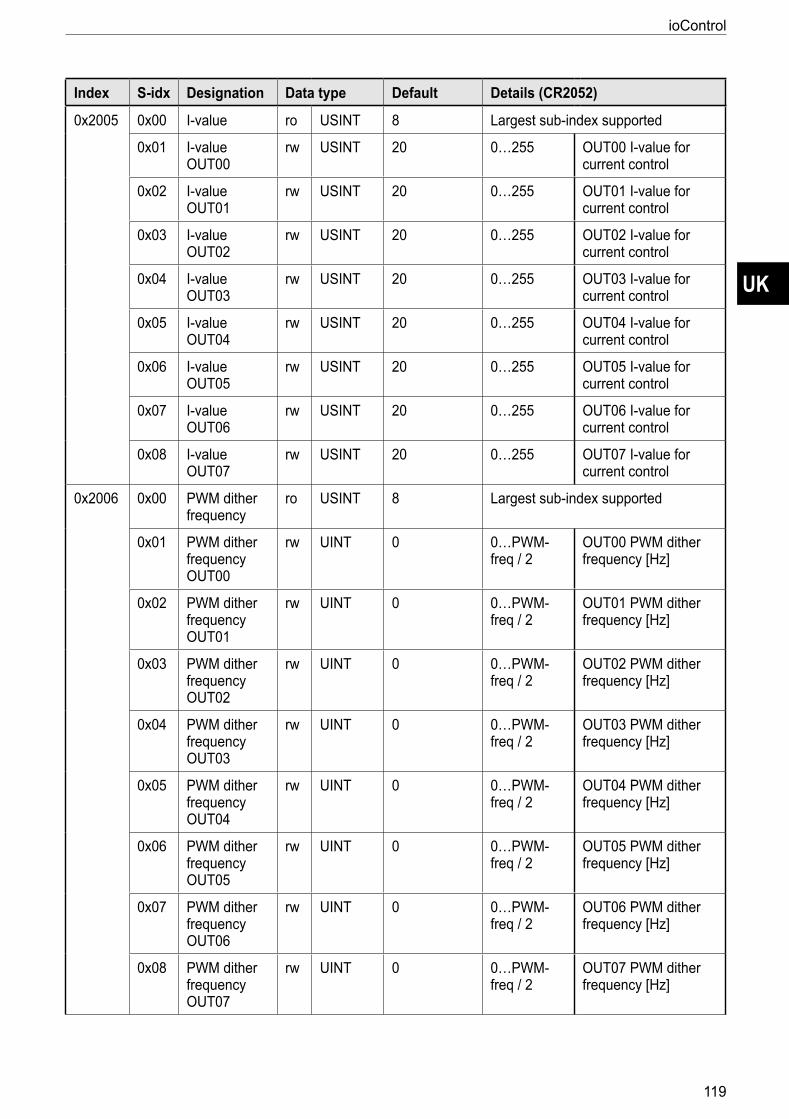
UK
ioControl
119
Index S-idx Designation Data type Default Details (CR2052)
0x2005 0x00 I-value ro USINT 8 Largest sub-index supported
0x01 I-value OUT00
rw USINT 20 0…255 OUT00 I-value for current control
0x02 I-value OUT01
rw USINT 20 0…255 OUT01 I-value for current control
0x03 I-value OUT02
rw USINT 20 0…255 OUT02 I-value for current control
0x04 I-value OUT03
rw USINT 20 0…255 OUT03 I-value for current control
0x05 I-value OUT04
rw USINT 20 0…255 OUT04 I-value for current control
0x06 I-value OUT05
rw USINT 20 0…255 OUT05 I-value for current control
0x07 I-value OUT06
rw USINT 20 0…255 OUT06 I-value for current control
0x08 I-value OUT07
rw USINT 20 0…255 OUT07 I-value for current control
0x2006 0x00 PWM dither frequency
ro USINT 8 Largest sub-index supported
0x01 PWM dither frequency OUT00
rw UINT 0 0…PWM-freq / 2
OUT00 PWM dither frequency [Hz]
0x02 PWM dither frequency OUT01
rw UINT 0 0…PWM-freq / 2
OUT01 PWM dither frequency [Hz]
0x03 PWM dither frequency OUT02
rw UINT 0 0…PWM-freq / 2
OUT02 PWM dither frequency [Hz]
0x04 PWM dither frequency OUT03
rw UINT 0 0…PWM-freq / 2
OUT03 PWM dither frequency [Hz]
0x05 PWM dither frequency OUT04
rw UINT 0 0…PWM-freq / 2
OUT04 PWM dither frequency [Hz]
0x06 PWM dither frequency OUT05
rw UINT 0 0…PWM-freq / 2
OUT05 PWM dither frequency [Hz]
0x07 PWM dither frequency OUT06
rw UINT 0 0…PWM-freq / 2
OUT06 PWM dither frequency [Hz]
0x08 PWM dither frequency OUT07
rw UINT 0 0…PWM-freq / 2
OUT07 PWM dither frequency [Hz]
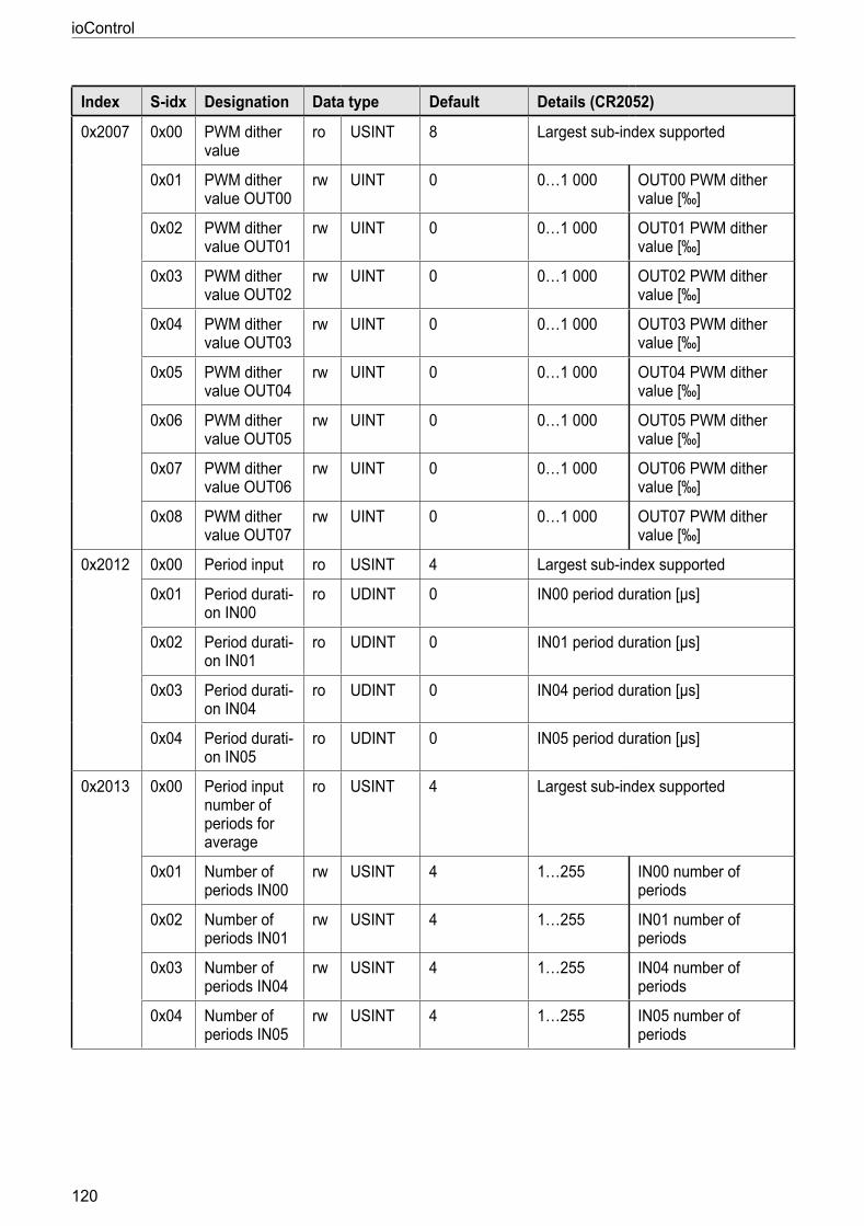
ioControl
120
Index S-idx Designation Data type Default Details (CR2052)
0x2007 0x00 PWM dither value
ro USINT 8 Largest sub-index supported
0x01 PWM dither value OUT00
rw UINT 0 0…1 000 OUT00 PWM dither value [‰]
0x02 PWM dither value OUT01
rw UINT 0 0…1 000 OUT01 PWM dither value [‰]
0x03 PWM dither value OUT02
rw UINT 0 0…1 000 OUT02 PWM dither value [‰]
0x04 PWM dither value OUT03
rw UINT 0 0…1 000 OUT03 PWM dither value [‰]
0x05 PWM dither value OUT04
rw UINT 0 0…1 000 OUT04 PWM dither value [‰]
0x06 PWM dither value OUT05
rw UINT 0 0…1 000 OUT05 PWM dither value [‰]
0x07 PWM dither value OUT06
rw UINT 0 0…1 000 OUT06 PWM dither value [‰]
0x08 PWM dither value OUT07
rw UINT 0 0…1 000 OUT07 PWM dither value [‰]
0x2012 0x00 Period input ro USINT 4 Largest sub-index supported
0x01 Period durati-on IN00
ro UDINT 0 IN00 period duration [µs]
0x02 Period durati-on IN01
ro UDINT 0 IN01 period duration [µs]
0x03 Period durati-on IN04
ro UDINT 0 IN04 period duration [µs]
0x04 Period durati-on IN05
ro UDINT 0 IN05 period duration [µs]
0x2013 0x00 Period input number of periods for average
ro USINT 4 Largest sub-index supported
0x01 Number of periods IN00
rw USINT 4 1…255 IN00 number of periods
0x02 Number of periods IN01
rw USINT 4 1…255 IN01 number of periods
0x03 Number of periods IN04
rw USINT 4 1…255 IN04 number of periods
0x04 Number of periods IN05
rw USINT 4 1…255 IN05 number of periods
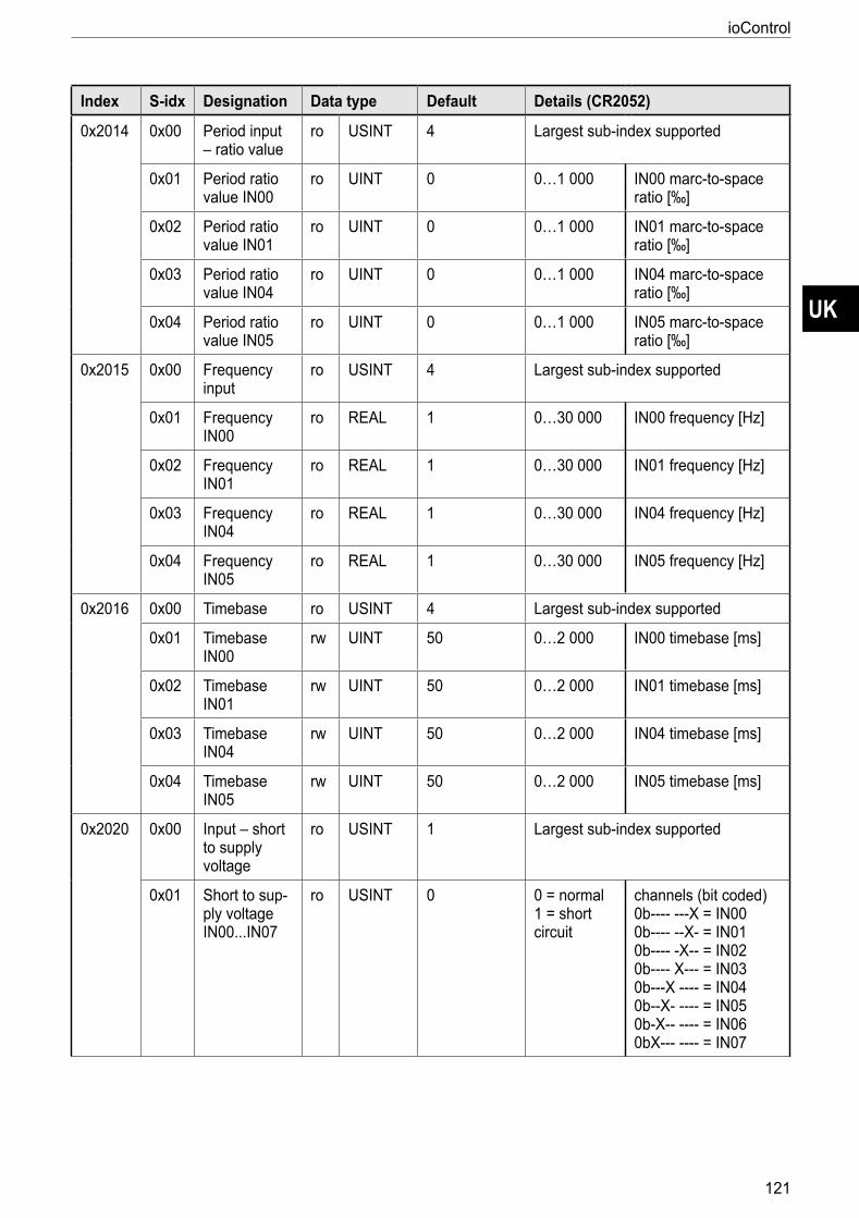
UK
ioControl
121
Index S-idx Designation Data type Default Details (CR2052)
0x2014 0x00 Period input – ratio value
ro USINT 4 Largest sub-index supported
0x01 Period ratio value IN00
ro UINT 0 0…1 000 IN00 marc-to-space ratio [‰]
0x02 Period ratio value IN01
ro UINT 0 0…1 000 IN01 marc-to-space ratio [‰]
0x03 Period ratio value IN04
ro UINT 0 0…1 000 IN04 marc-to-space ratio [‰]
0x04 Period ratio value IN05
ro UINT 0 0…1 000 IN05 marc-to-space ratio [‰]
0x2015 0x00 Frequency input
ro USINT 4 Largest sub-index supported
0x01 Frequency IN00
ro REAL 1 0…30 000 IN00 frequency [Hz]
0x02 Frequency IN01
ro REAL 1 0…30 000 IN01 frequency [Hz]
0x03 Frequency IN04
ro REAL 1 0…30 000 IN04 frequency [Hz]
0x04 Frequency IN05
ro REAL 1 0…30 000 IN05 frequency [Hz]
0x2016 0x00 Timebase ro USINT 4 Largest sub-index supported
0x01 Timebase IN00
rw UINT 50 0…2 000 IN00 timebase [ms]
0x02 Timebase IN01
rw UINT 50 0…2 000 IN01 timebase [ms]
0x03 Timebase IN04
rw UINT 50 0…2 000 IN04 timebase [ms]
0x04 Timebase IN05
rw UINT 50 0…2 000 IN05 timebase [ms]
0x2020 0x00 Input – short to supply voltage
ro USINT 1 Largest sub-index supported
0x01 Short to sup-ply voltage IN00IN07
ro USINT 0 0 = normal 1 = short circuit
channels (bit coded) 0b---- ---X = IN00 0b---- --X- = IN01 0b---- -X-- = IN02 0b---- X--- = IN03 0b---X ---- = IN04 0b--X- ---- = IN05 0b-X-- ---- = IN06 0bX--- ---- = IN07
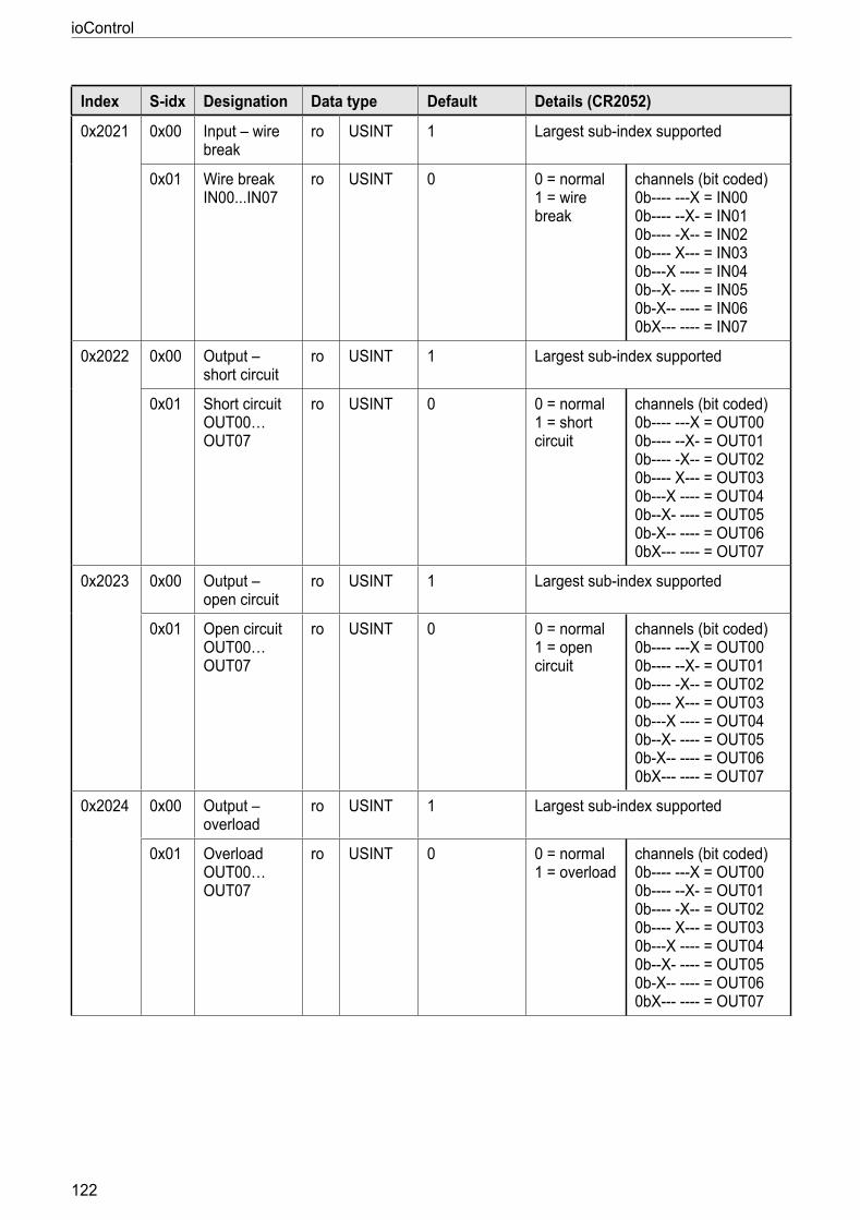
ioControl
122
Index S-idx Designation Data type Default Details (CR2052)
0x2021 0x00 Input – wire break
ro USINT 1 Largest sub-index supported
0x01 Wire break IN00IN07
ro USINT 0 0 = normal 1 = wire break
channels (bit coded) 0b---- ---X = IN00 0b---- --X- = IN01 0b---- -X-- = IN02 0b---- X--- = IN03 0b---X ---- = IN04 0b--X- ---- = IN05 0b-X-- ---- = IN06 0bX--- ---- = IN07
0x2022 0x00 Output – short circuit
ro USINT 1 Largest sub-index supported
0x01 Short circuit OUT00…OUT07
ro USINT 0 0 = normal 1 = short circuit
channels (bit coded) 0b---- ---X = OUT00 0b---- --X- = OUT01 0b---- -X-- = OUT02 0b---- X--- = OUT03 0b---X ---- = OUT04 0b--X- ---- = OUT05 0b-X-- ---- = OUT06 0bX--- ---- = OUT07
0x2023 0x00 Output – open circuit
ro USINT 1 Largest sub-index supported
0x01 Open circuit OUT00…OUT07
ro USINT 0 0 = normal 1 = open circuit
channels (bit coded) 0b---- ---X = OUT00 0b---- --X- = OUT01 0b---- -X-- = OUT02 0b---- X--- = OUT03 0b---X ---- = OUT04 0b--X- ---- = OUT05 0b-X-- ---- = OUT06 0bX--- ---- = OUT07
0x2024 0x00 Output – overload
ro USINT 1 Largest sub-index supported
0x01 Overload OUT00…OUT07
ro USINT 0 0 = normal 1 = overload
channels (bit coded) 0b---- ---X = OUT00 0b---- --X- = OUT01 0b---- -X-- = OUT02 0b---- X--- = OUT03 0b---X ---- = OUT04 0b--X- ---- = OUT05 0b-X-- ---- = OUT06 0bX--- ---- = OUT07
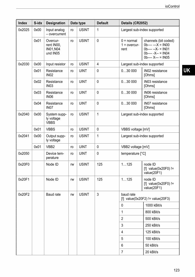
UK
ioControl
123
Index S-idx Designation Data type Default Details (CR2052)
0x2025 0x00 Input analog – overcurrent
ro USINT 1 Largest sub-index supported
0x01 Overcur-rent IN00, IN01,N04 und IN05
ro USINT 0 0 = normal 1 = overcur-rent
channels (bit coded) 0b---- ---X = IN00 0b---- --X- = IN01 0b---- -X-- = IN04 0b---- X--- = IN05
0x2030 0x00 Input resistor ro USINT 4 Largest sub-index supported
0x01 Resistance IN02
ro UINT 0 0…30 000 IN02 resistance [Ohms]
0x02 Resistance IN03
ro UINT 0 0…30 000 IN03 resistance [Ohms]
0x03 Resistance IN06
ro UINT 0 0…30 000 IN06 resistance [Ohms]
0x04 Resistance IN07
ro UINT 0 0…30 000 IN07 resistance [Ohms]
0x2040 0x00 System supp-ly voltage VBBS
ro USINT 1 Largest sub-index supported
0x01 VBBS ro USINT 0 VBBS voltage [mV]
0x2041 0x00 Output supp-ly voltage
ro USINT 1 Largest sub-index supported
0x01 VBB2 ro UINT 0 VBB2 voltage [mV]
0x2050 Device tem-perature
ro UINT 0 temperature [°C]
0x20F0 Node ID rw USINT 125 1…125 node ID [!] value(0x20F0) != value(20F1)
0x20F1 Node ID rw USINT 125 1…125 node ID [!] value(0x20F0) != value(20F1)
0x20F2 Baud rate rw USINT 3 baud rate [!] value(0x20F2) != value(20F3)
0 1000 kBit/s
1 800 kBit/s
2 500 kBit/s
3 250 kBit/s
4 125 kBit/s
5 100 kBit/s
6 50 kBit/s
7 20 kBit/s
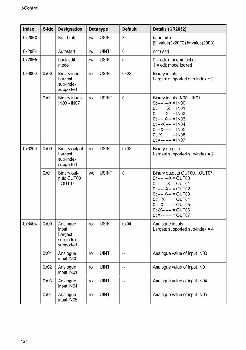
ioControl
124
Index S-idx Designation Data type Default Details (CR2052)
0x20F3 Baud rate rw USINT 3 baud rate [!] value(0x20F2) != value(20F3)
0x20F4 Autostart rw UINT 0 not used
0x20F5 Lock edit mode
rw USINT 0 0 = edit mode unlocked 1 = edit mode locked
0x6000 0x00 Binary input Largest sub-index supported
ro USINT 0x02 Binary inputs Largest supported sub-index = 2
0x01 Binary inputs IN00 - IN07
ro USINT 0 Binary inputs IN00…IN07 0b---- ---X = IN00 0b---- --X- = IN01 0b---- -X-- = IN02 0b---- X--- = IN03 0b---X ---- = IN04 0b--X- ---- = IN05 0b-X-- ---- = IN06 0bX--- ---- = IN07
0x6200 0x00 Binary output Largest sub-index supported
ro USINT 0x02 Binary outputs Largest supported sub-index = 2
0x01 Binary out-puts OUT00 - OUT07
wo USINT 0 Binary outputs OUT00…OUT07 0b---- ---X = OUT00 0b---- --X- = OUT01 0b---- -X-- = OUT02 0b---- X--- = OUT03 0b---X ---- = OUT04 0b--X- ---- = OUT05 0b-X-- ---- = OUT06 0bX--- ---- = OUT07
0x6404 0x00 Analogue input Largest sub-index supported
ro USINT 0x04 Analogue inputs Largest supported sub-index = 4
0x01 Analogue input IN00
ro UINT -- Analogue value of input IN00
0x02 Analogue input IN01
ro UINT -- Analogue value of input IN01
0x03 Analogue input IN04
ro UINT -- Analogue value of input IN04
0x04 Analogue input IN05
ro UINT -- Analogue value of input IN05
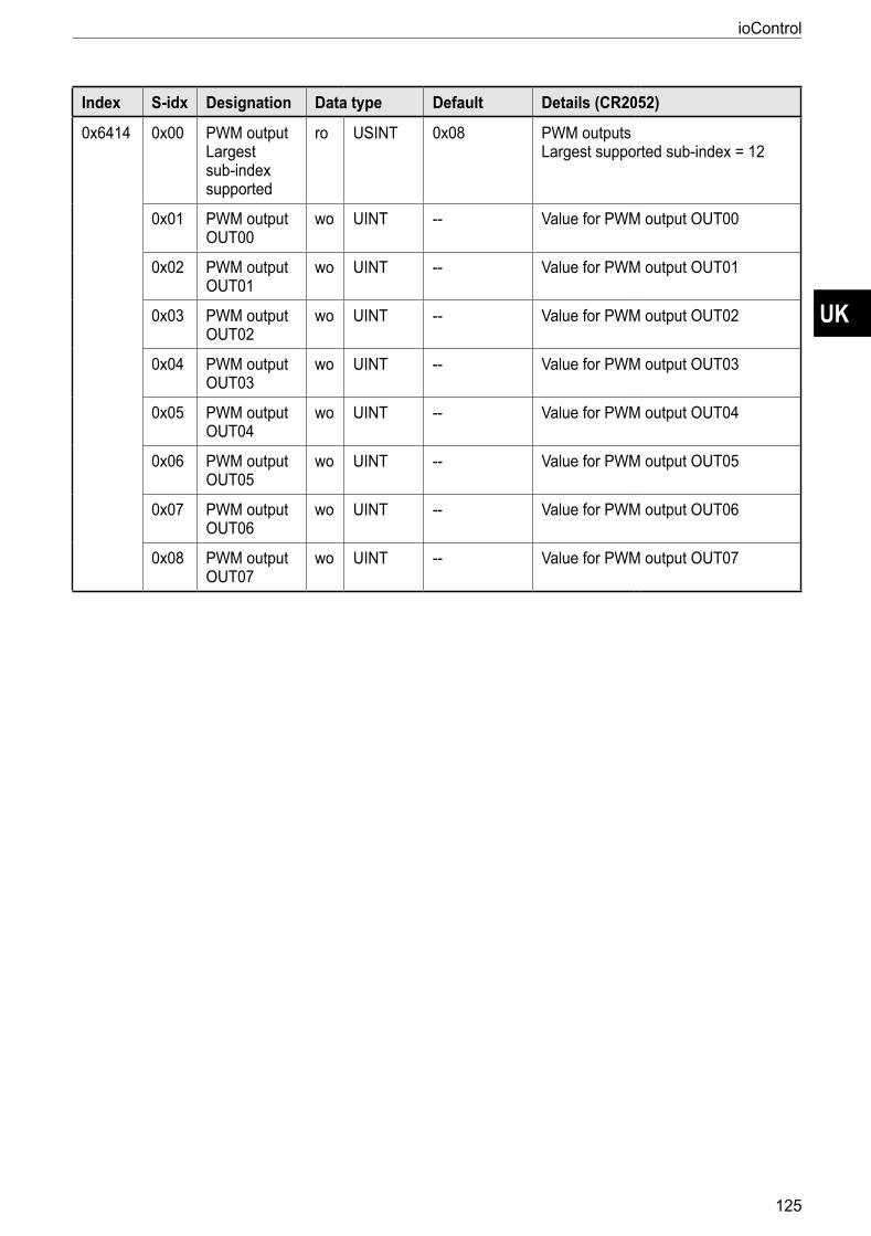
UK
ioControl
125
Index S-idx Designation Data type Default Details (CR2052)
0x6414 0x00 PWM output Largest sub-index supported
ro USINT 0x08 PWM outputs Largest supported sub-index = 12
0x01 PWM output OUT00
wo UINT -- Value for PWM output OUT00
0x02 PWM output OUT01
wo UINT -- Value for PWM output OUT01
0x03 PWM output OUT02
wo UINT -- Value for PWM output OUT02
0x04 PWM output OUT03
wo UINT -- Value for PWM output OUT03
0x05 PWM output OUT04
wo UINT -- Value for PWM output OUT04
0x06 PWM output OUT05
wo UINT -- Value for PWM output OUT05
0x07 PWM output OUT06
wo UINT -- Value for PWM output OUT06
0x08 PWM output OUT07
wo UINT -- Value for PWM output OUT07
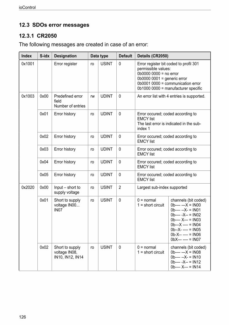
ioControl
126
12.3 SDOs error messages
12.3.1 CR2050The following messages are created in case of an error:
Index S-idx Designation Data type Default Details (CR2050)
0x1001 Error register ro USINT 0 Error register bit coded to profil 301 permissible values: 0b0000 0000 = no error 0b0000 0001 = generic error 0b0001 0000 = communication error 0b1000 0000 = manufacturer specific
0x1003 0x00 Predefined error field Number of entries
rw UDINT 0 An error list with 4 entries is supported
0x01 Error history ro UDINT 0 Error occured; coded according to EMCY list The last error is indicated in the sub-index 1
0x02 Error history ro UDINT 0 Error occured; coded according to EMCY list
0x03 Error history ro UDINT 0 Error occured; coded according to EMCY list
0x04 Error history ro UDINT 0 Error occured; coded according to EMCY list
0x05 Error history ro UDINT 0 Error occured; coded according to EMCY list
0x2020 0x00 Input – short to supply voltage
ro USINT 2 Largest sub-index supported
0x01 Short to supply voltage IN00IN07
ro USINT 0 0 = normal 1 = short circuit
channels (bit coded) 0b---- ---X = IN00 0b---- --X- = IN01 0b---- -X-- = IN02 0b---- X--- = IN03 0b---X ---- = IN04 0b--X- ---- = IN05 0b-X-- ---- = IN06 0bX--- ---- = IN07
0x02 Short to supply voltage IN08, IN10, IN12, IN14
ro USINT 0 0 = normal 1 = short circuit
channels (bit coded) 0b---- ---X = IN08 0b---- --X- = IN10 0b---- -X-- = IN12 0b---- X--- = IN14
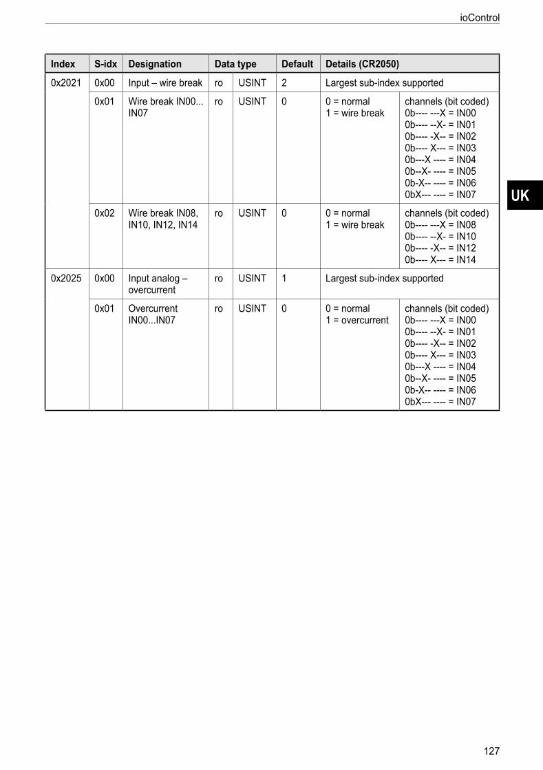
UK
ioControl
127
Index S-idx Designation Data type Default Details (CR2050)
0x2021 0x00 Input – wire break ro USINT 2 Largest sub-index supported
0x01 Wire break IN00IN07
ro USINT 0 0 = normal 1 = wire break
channels (bit coded) 0b---- ---X = IN00 0b---- --X- = IN01 0b---- -X-- = IN02 0b---- X--- = IN03 0b---X ---- = IN04 0b--X- ---- = IN05 0b-X-- ---- = IN06 0bX--- ---- = IN07
0x02 Wire break IN08, IN10, IN12, IN14
ro USINT 0 0 = normal 1 = wire break
channels (bit coded) 0b---- ---X = IN08 0b---- --X- = IN10 0b---- -X-- = IN12 0b---- X--- = IN14
0x2025 0x00 Input analog – overcurrent
ro USINT 1 Largest sub-index supported
0x01 Overcurrent IN00IN07
ro USINT 0 0 = normal 1 = overcurrent
channels (bit coded) 0b---- ---X = IN00 0b---- --X- = IN01 0b---- -X-- = IN02 0b---- X--- = IN03 0b---X ---- = IN04 0b--X- ---- = IN05 0b-X-- ---- = IN06 0bX--- ---- = IN07
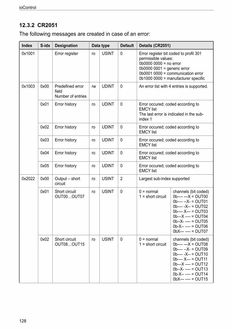
ioControl
128
12.3.2 CR2051The following messages are created in case of an error:
Index S-idx Designation Data type Default Details (CR2051)
0x1001 Error register ro USINT 0 Error register bit coded to profil 301 permissible values: 0b0000 0000 = no error 0b0000 0001 = generic error 0b0001 0000 = communication error 0b1000 0000 = manufacturer specific
0x1003 0x00 Predefined error field Number of entries
rw UDINT 0 An error list with 4 entries is supported
0x01 Error history ro UDINT 0 Error occured; coded according to EMCY list The last error is indicated in the sub-index 1
0x02 Error history ro UDINT 0 Error occured; coded according to EMCY list
0x03 Error history ro UDINT 0 Error occured; coded according to EMCY list
0x04 Error history ro UDINT 0 Error occured; coded according to EMCY list
0x05 Error history ro UDINT 0 Error occured; coded according to EMCY list
0x2022 0x00 Output – short circuit
ro USINT 2 Largest sub-index supported
0x01 Short circuit OUT00…OUT07
ro USINT 0 0 = normal 1 = short circuit
channels (bit coded) 0b---- ---X = OUT00 0b---- --X- = OUT01 0b---- -X-- = OUT02 0b---- X--- = OUT03 0b---X ---- = OUT04 0b--X- ---- = OUT05 0b-X-- ---- = OUT06 0bX--- ---- = OUT07
0x02 Short circuit OUT08…OUT15
ro USINT 0 0 = normal 1 = short circuit
channels (bit coded) 0b---- ---X = OUT08 0b---- --X- = OUT09 0b---- -X-- = OUT10 0b---- X--- = OUT11 0b---X ---- = OUT12 0b--X- ---- = OUT13 0b-X-- ---- = OUT14 0bX--- ---- = OUT15
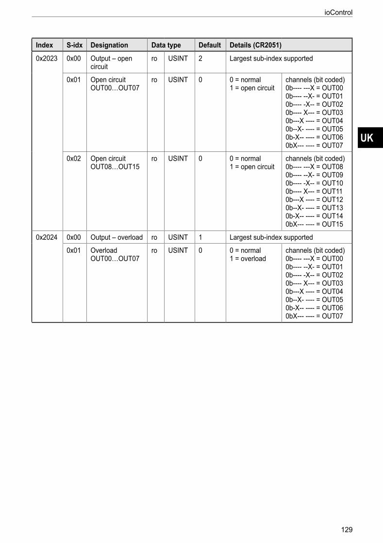
UK
ioControl
129
Index S-idx Designation Data type Default Details (CR2051)
0x2023 0x00 Output – open circuit
ro USINT 2 Largest sub-index supported
0x01 Open circuit OUT00…OUT07
ro USINT 0 0 = normal 1 = open circuit
channels (bit coded) 0b---- ---X = OUT00 0b---- --X- = OUT01 0b---- -X-- = OUT02 0b---- X--- = OUT03 0b---X ---- = OUT04 0b--X- ---- = OUT05 0b-X-- ---- = OUT06 0bX--- ---- = OUT07
0x02 Open circuit OUT08…OUT15
ro USINT 0 0 = normal 1 = open circuit
channels (bit coded) 0b---- ---X = OUT08 0b---- --X- = OUT09 0b---- -X-- = OUT10 0b---- X--- = OUT11 0b---X ---- = OUT12 0b--X- ---- = OUT13 0b-X-- ---- = OUT14 0bX--- ---- = OUT15
0x2024 0x00 Output – overload ro USINT 1 Largest sub-index supported
0x01 Overload OUT00…OUT07
ro USINT 0 0 = normal 1 = overload
channels (bit coded) 0b---- ---X = OUT00 0b---- --X- = OUT01 0b---- -X-- = OUT02 0b---- X--- = OUT03 0b---X ---- = OUT04 0b--X- ---- = OUT05 0b-X-- ---- = OUT06 0bX--- ---- = OUT07
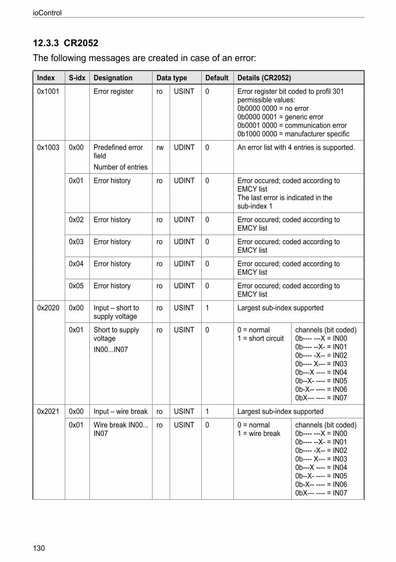
ioControl
130
12.3.3 CR2052The following messages are created in case of an error:
Index S-idx Designation Data type Default Details (CR2052)
0x1001 Error register ro USINT 0 Error register bit coded to profil 301 permissible values: 0b0000 0000 = no error 0b0000 0001 = generic error 0b0001 0000 = communication error 0b1000 0000 = manufacturer specific
0x1003 0x00 Predefined error fieldNumber of entries
rw UDINT 0 An error list with 4 entries is supported
0x01 Error history ro UDINT 0 Error occured; coded according to EMCY list The last error is indicated in the sub-index 1
0x02 Error history ro UDINT 0 Error occured; coded according to EMCY list
0x03 Error history ro UDINT 0 Error occured; coded according to EMCY list
0x04 Error history ro UDINT 0 Error occured; coded according to EMCY list
0x05 Error history ro UDINT 0 Error occured; coded according to EMCY list
0x2020 0x00 Input – short to supply voltage
ro USINT 1 Largest sub-index supported
0x01 Short to supply voltageIN00IN07
ro USINT 0 0 = normal 1 = short circuit
channels (bit coded) 0b---- ---X = IN00 0b---- --X- = IN01 0b---- -X-- = IN02 0b---- X--- = IN03 0b---X ---- = IN04 0b--X- ---- = IN05 0b-X-- ---- = IN06 0bX--- ---- = IN07
0x2021 0x00 Input – wire break ro USINT 1 Largest sub-index supported
0x01 Wire break IN00IN07
ro USINT 0 0 = normal 1 = wire break
channels (bit coded) 0b---- ---X = IN00 0b---- --X- = IN01 0b---- -X-- = IN02 0b---- X--- = IN03 0b---X ---- = IN04 0b--X- ---- = IN05 0b-X-- ---- = IN06 0bX--- ---- = IN07
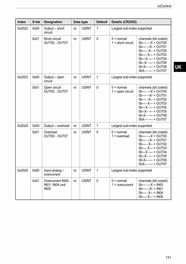
UK
ioControl
131
Index S-idx Designation Data type Default Details (CR2052)
0x2022 0x00 Output – short circuit
ro USINT 1 Largest sub-index supported
0x01 Short circuit OUT00…OUT07
ro USINT 0 0 = normal 1 = short circuit
channels (bit coded) 0b---- ---X = OUT00 0b---- --X- = OUT01 0b---- -X-- = OUT02 0b---- X--- = OUT03 0b---X ---- = OUT04 0b--X- ---- = OUT05 0b-X-- ---- = OUT06 0bX--- ---- = OUT07
0x2023 0x00 Output – open circuit
ro USINT 1 Largest sub-index supported
0x01 Open circuit OUT00…OUT07
ro USINT 0 0 = normal 1 = open circuit
channels (bit coded) 0b---- ---X = OUT00 0b---- --X- = OUT01 0b---- -X-- = OUT02 0b---- X--- = OUT03 0b---X ---- = OUT04 0b--X- ---- = OUT05 0b-X-- ---- = OUT06 0bX--- ---- = OUT07
0x2024 0x00 Output – overload ro USINT 1 Largest sub-index supported
0x01 Overload OUT00…OUT07
ro USINT 0 0 = normal 1 = overload
channels (bit coded) 0b---- ---X = OUT00 0b---- --X- = OUT01 0b---- -X-- = OUT02 0b---- X--- = OUT03 0b---X ---- = OUT04 0b--X- ---- = OUT05 0b-X-- ---- = OUT06 0bX--- ---- = OUT07
0x2025 0x00 Input analog – overcurrent
ro USINT 1 Largest sub-index supported
0x01 Overcurrent IN00, IN01, IN04 und IN05
ro USINT 0 0 = normal 1 = overcurrent
channels (bit coded) 0b---- ---X = IN00 0b---- --X- = IN01 0b---- -X-- = IN04 0b---- X--- = IN05