Embed Size (px)
Citation preview

�
�
Linköping Studies in Science and Technology
Dissertation No. 1317
Development of Organic-Based
Thin Film Magnets for Spintronics
Elin Carlegrim
Department of Physics, Chemistry and Biology
Linköping University, SE-581 83 Linköping, Sweden
Linköping 2010

�
�
ISBN: 978-91-7393-385-8
ISSN: 0345-7524
Copyright © Elin Carlegrim, 2010, unless otherwise noted
Printed by LiU-Tryck, Linköping, Sweden, 2010
�
�
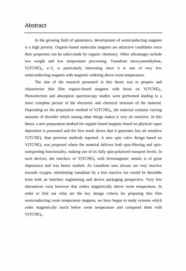
Abstract
In the growing field of spintronics, development of semiconducting magnets
is a high priority. Organic-based molecular magnets are attractive candidates since
their properties can be tailor-made by organic chemistry. Other advantages include
low weight and low temperature processing. Vanadium tetracyanoethylene,
V(TCNE)x, x~2, is particularly interesting since it is one of very few
semiconducting magnets with magnetic ordering above room temperature.
The aim of the research presented in this thesis was to prepare and
characterize thin film organic-based magnets with focus on V(TCNE)x.
Photoelectron and absorption spectroscopy studies were performed leading to a
more complete picture of the electronic and chemical structure of the material.
Depending on the preparation method of V(TCNE)x, the material contains varying
amounts of disorder which among other things makes it very air sensitive. In this
thesis, a new preparation method for organic-based magnets based on physical vapor
deposition is presented and the first result shows that it generates less air sensitive
V(TCNE)x than previous methods reported. A new spin valve design based on
V(TCNE)x was proposed where the material delivers both spin-filtering and spin-
transporting functionality, making use of its fully spin-polarized transport levels. In
such devices, the interface of V(TCNE)x with ferromagnetic metals is of great
importance and was hence studied. As vanadium ions always are very reactive
towards oxygen, substituting vanadium by a less reactive ion would be desirable
from both an interface engineering and device packaging perspective. Very few
alternatives exist however that orders magnetically above room temperature. In
order to find out what are the key design criteria for preparing thin film
semiconducting room temperature magnets, we have begun to study systems which
order magnetically much below room temperature and compared them with
V(TCNE)x.

�
�
�
�
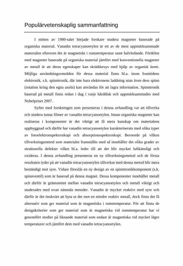
Populärvetenskaplig sammanfattning
I mitten av 1980-talet började forskare studera magneter baserade på
organiska material. Vanadin tetracyanoetylen är ett av de mest uppmärksammade
materialen eftersom det är magnetiskt i rumstemperatur samt halvledande. Fördelen
med magneter baserade på organiska material jämfört med konventionella magneter
av metall är att deras egenskaper kan skräddarsys med hjälp av organisk kemi.
Möjliga användningsområden för dessa material finns bl.a. inom framtidens
elektronik, s.k. spinntronik, där inte bara elektronens laddning utan även dess spinn
(rotation kring den egna axeln) kan användas för att lagra information. Spinntronik
baserad på metall finns redan i dag i varje hårddisk och uppmärksammades med
Nobelpriset 2007.
Syftet med forskningen som presenteras i denna avhandling var att tillverka
och studera tunna filmer av vanadin tetracyanoetylen. Innan organiska magneter kan
realiseras i komponenter är det viktigt att få mera kunskap om materialens
uppbyggnad och därför har vanadin tetracyanoetylen karakteriserats med olika typer
av fotoelektronspektroskopi och absorptionsspektroskopi. Beroende på vilken
tillverkningsmetod som materialet framställts med så innehåller det olika grader av
strukturella defekter vilket bl.a. leder till att det blir mycket luftkänsligt och
oxideras. I denna avhandling presenteras en ny tillverkningsmetod och de första
resultaten tyder på att vanadin tetracyanoetylen tillverkat med denna metod blir mera
beständigt mot syre. Vidare föreslås en ny design av en spinntronikkomponent (s.k.
spinnventil) som är baserad på denna magnet. Dessa komponenter innehåller metall
och därför är gränssnittet mellan vanadin tetracyanoetylen och metall viktigt och
studerades med ovan nämnda metoder. Vanadin är mycket reaktivt med syre och
därför är det önskvärt att byta ut det mot en mindre reaktiv metall, dock finns det få
alternativ som ger material som är magnetiska i rumstemperatur. För att finna de
designkriterier som ger material som är magnetiska vid rumstemperatur har vi
genomfört studier på liknande material som endast är magnetiska vid mycket lägre
temperaturer och jämfört dem med vanadin tetracyanoetylen.

�
�
�
�
Preface
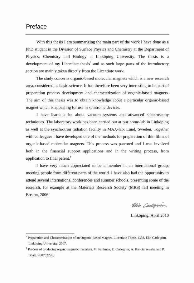
With this thesis I am summarizing the main part of the work I have done as a
PhD student in the Division of Surface Physics and Chemistry at the Department of
Physics, Chemistry and Biology at Linköping University. The thesis is a
development of my Licentiate thesis* and as such large parts of the introductory
section are mainly taken directly from the Licentiate work.
The study concerns organic-based molecular magnets which is a new research
area, considered as basic science. It has therefore been very interesting to be part of
preparation process development and characterization of organic-based magnets.
The aim of this thesis was to obtain knowledge about a particular organic-based
magnet which is appealing for use in spintronic devices.
I have learnt a lot about vacuum systems and advanced spectroscopy
techniques. The laboratory work has been carried out at our home-lab in Linköping
as well at the synchrotron radiation facility in MAX-lab, Lund, Sweden. Together
with colleagues I have developed one of the methods for preparation of thin films of
organic-based molecular magnets. This process was patented and I was involved
both in the financial support applications and in the writing process, from
application to final patent.†
I have very much appreciated to be a member in an international group,
meeting people from different parts of the world. I have also had the opportunity to
attend several international conferences and summer schools, presenting some of the
research, for example at the Materials Research Society (MRS) fall meeting in
Boston, 2006.
Linköping, April 2010
�����������������������������������������* Preparation and Characterization of an Organic-Based Magnet, Licentiate Thesis 1338, Elin Carlegrim,
Linköping University, 2007. ��Process of producing organomagnetic materials, M. Fahlman, E. Carlegrim, A. Kanciurzewska and P.
Bhatt, SE0702226. �

�
�

�
�
Acknowledgements
This thesis would not have been realized without help and support from a
number of people and therefore I would like to thank:
• First of all, my supervisor Prof. Mats Fahlman for guidance, support and for
introducing me to the field of organic-based magnets and photoelectron
spectroscopy.
• All the members, past and present, of the Division of Surface Physics and
Chemistry for discussions and for help with lab equipment, but also for lunch
and coffee break discussions concerning other topics than research.
Especially, I would like to thank the people that have contributed to the
included papers in this thesis. I am also grateful to Linda Lindell for all
support in the end my PhD studies.
• My friends outside university, for sharing small and big things in life.
Particularly, I would like to mention Anna S, Maria and my sisters, Anna
and Sara.
• My parents, Ingrid and Börje for support and interest in what I am doing.
Last, but not least, Anders, Elsa and the fourth family member on its way for
reminding me everyday of what is most important in life.

�
�

�
�
Papers Included in the Thesis�
Paper I Near-edge x-ray absorption studies of Na-doped tetracyanoethylene films: A
model system for the V(TCNE)x room-temperature molecular magnet
E. Carlegrim, B. Gao, A. Kanciurzewska, M.P. de Jong, Z. Wu, Y. Luo and M.
Fahlman
Physical Review B 77, 054420 (2008)
Paper II The unoccupied electronic structure of the semi-conducting room temperature
molecular magnet V(TCNE)2
E. Carlegrim, A. Kanciurzewska, M.P. de Jong, C. Tengstedt and M. Fahlman
Chemical Physics Letters 452, 173 (2008)
Paper III Air-stable organic-based semiconducting room temperature thin film magnet
for spintronics applications
E. Carlegrim, A. Kanciurzewska, P. Nordblad and M. Fahlman
Applied Physics Letters 92, 163308 (2008)
Paper IV Characterization of the Ni/V(TCNE)x interface for hybrid spintronics
applications
E. Carlegrim, Y. Zhan, F. Li, X. Liu and M. Fahlman
Organic Electronics, in press
Paper V Electronic structure of thin film cobalt tetracyanoethylene, Co(TCNE)x
E. Carlegrim, Y. Zhan, M.P. de Jong and M. Fahlman
In manuscript

�
�

�
�
The Author’s Contribution to the Papers�
Paper I All the experimental work and data analysis in cooperation. Wrote the first draft and
was responsible for the iterative process to the final version. The theoretical work
was performed by collaborators at KTH, Stockholm.
Paper II All the experimental work and data analysis in cooperation. Wrote the first draft and
was responsible for the iterative process to the final version.
Paper III Development of the new preparation method, photoelectron spectroscopy studies
and data analysis in cooperation. Wrote the first draft and was responsible for the
iterative process to the final version. The SQUID measurements were performed by
P. Nordblad at Uppsala University.
Paper IV Major part of the experimental work and all of the data analysis. Wrote the first draft
and was responsible for the iterative process to the final version.
Paper V All the experimental work and data analysis. Wrote the first draft and was
responsible for the iterative process to the final version.

�
�
�
�
Related Papers not Included in the Thesis�
Photoelectron spectroscopy of the contact between the cathode and the active
layers in plastic solar cells: the role of LiF
S.K.M. Jönsson, E. Carlegrim, F. Zhang, W.R. Salaneck and M. Fahlman
Japanese Journal of Applied Physics 44, 3695 (2005)
X-ray magnetic circular dichroism and resonant photoemission of V(TCNE)x
hybrid magnets
C. Tengstedt, M.P. de Jong, A. Kanciurzewska, E. Carlegrim and M. Fahlman
Physical Review Letters 96, 057209 (2006)
Chemical bonding in V(TCNE)x (x~2) thin-film magnets grown in situ
M.P. de Jong, C. Tengstedt, A. Kanciurzewska, E. Carlegrim, W.R. Salaneck and M.
Fahlman
Physical Review B 75, 64407 (2007)
Study on Poly(3,4-ethylene dioxythiophene)-Poly(styrenesulfonate) as a plastic
counter electrode in dye sensitized solar cells
A. Kanciurzewska, E. Dobruchowska, A. Baranzahi, E. Carlegrim, M. Fahlman and
M.A. Gîr�u
Journal of Optoelectronics and Advanced Materials 9, 1052 (2007)
Process of producing organomagnetic materials
M. Fahlman, E. Carlegrim, A. Kanciurzewska and P. Bhatt
Patent number: SE0702226 (2007)
Electronic structure of thin film iron-tetracyanoethylene: Fe(TCNE)x
P. Bhatt, E. Carlegrim, A. Kanciurzewska, M.P. de Jong and M. Fahlman
Applied Physics A 95, 131 (2009)
�
�
Ferromagnetism above room temperature in nickel-tetracyanoethylene thin
films
P. Bhatt, A. Kanciurzewska, E. Carlegrim, M. Kapilashrami, L. Belova, K.V. Rao
and M. Fahlman
Journal of Materials Chemistry 19, 6610 (2009)
The role of aluminium oxide buffer layer in organic spin-valves performance
Y.Q. Zhan, X.J. Liu, E. Carlegrim, F.H. Li, I. Bergenti, P. Graziosi, V. Dediu, and
M. Fahlman
Applied Physics Letters 94, 053301 (2009)
Efficient spin injection through exchange coupling at organic
semiconductor/ferromagnet heterojunctions
Y. Zhan, E. Holmström, R. Lizárraga, O. Eriksson, X. Liu, F. Li, E. Carlegrim, S.
Stafström, and M. Fahlman
Advanced Materials 21, 1 (2009)
Experimental evidence for ferromagnetism at room-temperature in MgO thin
films
M. Kapilashrami, J. Xu, K.V. Rao, L. Belova, E. Carlegrim and M. Fahlman
Submitted
�
�
Contents
1 Introduction 1
2 Organic-Based Magnets 3
2.1 Origin of Magnetic Ordering and Interactions 3
2.1.1 Magnetic Ordering 4
2.1.2 Magnetic Interactions 5
2.1.3 Factors Influencing Magnetic Ordering 5
2.1.4 Definitions of Some Key Parameters in Magnetism 6
2.2 Materials 6
2.3 Spintronics 9
3 Preparation Methods 13
3.1 Solution-Based Preparation 13
3.2 Chemical Vapor Deposition (CVD) 14
3.3 Physical Vapor Deposition (PVD) 15
4 Experimental Techniques 17
4.1 Photoelectron Spectroscopy 17
4.1.1 The Principle of Photoionization 17
4.1.2 Core Level Spectroscopy (XPS) 19
4.1.3 Valence Level Spectroscopy (UPS) 21
4.1.4 Reference Level 22
4.1.5 Intensity and Resolution 23
4.2 Photon Sources 23
4.3 Absorption Spectroscopy 24
4.4 Resonant Photoelectron Spectroscopy (RPES) 26
4.5 Superconducting Quantum Interference Device (SQUID) 26
5 Equipment 29
5.1 Moses 29
5.2 Scienta 30
5.3 Beamline I311 31
5.4 Beamline D1011 32

�
�
6 Summary and Future Outlook 35
6.1 Background 35
6.2 Summary of the Thesis 36
6.3 Current Studies 41
6.4 Future Outlook 41
References 43
Paper I
Paper II
Paper III
Paper IV
Paper V
�
1
1 Introduction
Magnets based on organic materials, so-called organic-based molecular
magnets (OMMs), is a new and ‘exotic’ field of organic electronics1. In contrast to
conventional atom-based transition- and rare-earth-based metallic magnets, the basis
in organic-based magnets is molecules. The main advantage of these magnets is that
their magnetic and electronic properties can be tuned by molecular design. Other
advantages include conductivity ranging from semi-conducting to insulating, low
weight, low temperature processing, low environmental contamination etc.2, 3 Some
organic-based magnets also offer properties not seen in conventional magnets, such
as light-induced magnetism, solubility in organic solvents and biocompatibility.2-5
The belief in that organic magnets could exist was of theoretical nature, formulated
in the 1950s, but it took until the mid 1980s until the first organic-based magnets
were prepared.6 A breakthrough came 1991 when the first room temperature
organic-based magnet was discovered,7 opening the door to many potential
applications. In the same year also the first purely organic magnets were
discovered.8, 9 Once those materials are well characterized, they may very well be
used in both traditional applications and prospective applications not thought of yet.
Room temperature organic-based magnets could eventually be used as functional
coatings, for example frequency or magnetic shielding and anti-static coatings.10
One can also imagine less traditional applications in so-called spin-based
electronics11 (spintronics), such as memory devices, sensors, medicine carriers etc.
However, before this can be reality, deeper understanding in the physical and
chemical properties of the materials is required. Different electron spectroscopy
techniques, e.g. photoelectron spectroscopy (PES) and near edge X-ray absorption
fine structure (NEXAFS) spectroscopy, are well suited for characterization of the
surfaces and interfaces of the materials as the energy of photoexcited electrons give
� Chapter 1 Introduction
2
information regarding the electronic structure as well as chemical composition and
environment.
This thesis consists of an introductory part and a set of five included papers.
The introductory part provides an overview of organic-based molecular magnets,
their preparation methods, some of the experimental techniques used for studying
OMMs and a presentation of the equipment which have been utilized in this work.
Finally the work in this thesis is summarized and a future outlook is given. Hence,
the aim of the introductory part is to give a brief overview of the subject, while the
included papers reflect my contribution to the research field.
�
3
2 Organic-Based Magnets
In contrast to conventional atom-based magnets, which are based on
transition- or rare-earth metals with net spin in d- or f-orbitals, organic-based
magnets have net spins residing in p- or s-orbitals. Organic-based magnets can be
classified into two groups, purely organic or hybrid organic-inorganic. In the hybrid
organic-inorganic magnets, the organic part can be either passive, (without net spin)
or active (with net spin). Further, they can be divided into groups depending on the
number of metal ions, type of ligands and their lattice dimension, i.e. isolated
molecules (0D), chain (1D), layer (2D) or bulk networks (3D), etc.2 One of the most
extensively studied family of 3D organic-based magnets is transition-metal
tetracyanoethylene complexes, M(TCNE)x.7, 12-14 The large interest in these magnets
started with vanadium tetracyanoethylene, V(TCNE)x, which was the first organic-
based magnet to show magnetic ordering above room temperature.7 Since the main
focus in this thesis is V(TCNE)x, its properties and potential applications are
discussed in this chapter, after a short introduction to magnetism.
2.1 Origin of Magnetic Ordering and Interactions
The essential component of a magnetic material is the existence of un-paired
electrons, or more precisely spins associated with un-paired electrons (a net spin).
Magnetic ordering is a cooperative effect and these spins have to interact with each
other in order to create a magnetic material. This ordering effect of interaction has to
be larger than the disordering effect of thermal agitation. Hence, magnetic ordering
only occurs below a critical temperature, the so-called Curie temperature of ferro-
and ferrimagnets or Néel temperature of antiferromagnets.15, 16
Chapter 2 Organic-Based Magnets
4
2.1.1 Magnetic Ordering
The interaction of spins at nearby sites leads to different spin configurations,
namely, para-, ferro-, antiferro- and ferrimagnetism.17 In a paramagnet the spins are
aligned in different directions and those directions change rapidly with respect to
time, even at low temperatures. If an external field is applied, the spins (may) align
in the same direction. Besides, all ferro- antiferro- and ferrimagnetic materials
become paramagnetic above their critical temperature. A ferromagnet has a
spontaneous magnetization (net spin) even in absence of an external magnetic field
since the spins are aligned in the same direction below the Curie temperature. In an
antiferromagnetic material the spins are aligned anti-parallel to each other, leading
to a zero net spin.
PARAMAGNET FERROMAGNET
ANTIFERROMAGNET FERRIMAGNET
PARAMAGNETPARAMAGNET FERROMAGNETFERROMAGNET
ANTIFERROMAGNETANTIFERROMAGNET FERRIMAGNETFERRIMAGNET
Figure 2.1 Examples of different spin configurations in absence of an external field,
see e.g. Introduction to Solid State Physics by C. Kittel.17
Ferrimagnetism is a special case of antiferromagnetism and below their critical
temperature these materials have a net magnetic moment. Therefore, ferrimagnets
behave like ferromagnets at the macroscopic scale. It is important to note that those
behaviors discussed above are not a property of an individual molecule, they are
bulk properties.
Chapter 2 Organic-Based Magnets
5
2.1.2 Magnetic Interactions
The main type of magnetic interaction is the Heisenberg exchange
interaction.2, 3 The Heisenberg effect is a quantum effect and is mainly due to the
Pauli’s exclusion principle. Other types of magnetic interactions (e.g. dipole
interaction) are generally neglected.3 The pair-wise spin interaction in (ferro- and
antiferro-) magnetic systems at a zero applied magnetic field may be described by
the Heisenberg Hamiltonian:
jiji,Jji,
2H SS ⋅−= � (2.1)
where i and j are independent of directions (x, y or z) of the nearest-neighbor sites
and S i · S j is the scalar product of these adjacent vector spins. J i,j is the exchange
constant (ferromagnetic, J>0, or antiferromagnetic, J<0), summing over all possible
interactions. However, this is a basic picture and further contributions can be
accounted for and added to the equation.2, 18 Since organic-based magnets often are
disordered, a term representing random magnetic anisotropy (see paragraph below)
is sometimes included into the equation:
2)(
,�� ⋅−⋅−=i
iirDjiji
ji,J2H SnSS (2.2)
where Dr is a measure of the random anisotropy strength and ni is a unit vector that
corresponds to a random field, pointing in the direction of local anisotropy.2
2.1.3 Factors Influencing Magnetic Ordering
The main factors influencing the magnetic ordering are spin dimensionality,
lattice dimensionality, spin value but also disorder and frustration.18 An example of
disorder frequently occurring in magnetic amorphous solids (e.g. hybrid organic-
inorganic compounds) is random magnetic anisotropy,19 i.e. different magnetic
interaction in different directions. Frustration is another phenomenon typical of
organic-based magnets, where a spin system cannot minimize the energy of each
spin pair in a network, simultaneously.18 This leads to peculiar magnetic phenomena
Chapter 2 Organic-Based Magnets
6
at low temperatures, e.g. spin glass state,2, 3 since the direction of the spins locally
freezes and changes their orientation extremely slowly with respect to time below a
certain temperature.14 Spin glass behavior is commonly occurring for organic-based
magnets, e.g. V(TCNE)x powder magnets (see chapter 3).
2.1.4 Definitions of Some Key Parameters in Magnetism
Susceptibility, coercivity and remanence are three important parameters when
describing the magnetization of a material. The susceptibility is used to describe the
response of a material to an applied field. The coercivity describes the required
intensity of an applied magnetic field to completely demagnetize a magnetic
material which has been magnetized to saturation. When the coercive field of a
magnet is large, the material is said to be hard (permanent magnets), while if the
coercive field is low, the magnet is known to be soft. The remanence is a measure of
the magnetization of a magnetic material after an external field has been removed.
Both the coercivity and remanence can be illustrated by a so-called hysteresis
curve.16
2.2 Materials
M(TCNE)x, where M = V, Fe, Mn, Co, Ni etc., TCNE = tetracyanoethylene,
x~2,7, 12-14, 20 is one of the most studied families of organic-based magnets. Recently,
it has been extended to also include Cr, Nb and Mo.21 An unlimited number of
variants of M(organic molecule)x can be prepared by exchanging the metal, or the
organic molecule,22-24 as well as both. Combination of metals, i.e. M’zM’’1-
z(TCNE)x, 0<z<1, has also been reported,25-27 some of them showing Curie
temperatures above room temperature. Moreover, the stoichiometry of the species in
M(TCNE)x can be varied, such that x deviates from 2, while still obtaining magnetic
ordering above room temperature.28 However, if this is correct or if the room
temperature magnetic ordering in those M(TCNE)x magnets are due to other factors
are still under debate.29, 30
Particularly V(TCNE)x has caught the interest since it was the first room
temperature (TC is close to 400 K) organic-based magnet when reported in 1991.7
Unfortunately, the material is extremely air sensitive and this, together with its
disordered structure, has hindered and delayed studies of the material. The magnet
Chapter 2 Organic-Based Magnets
7
can be prepared either as a powder or as a thin film (see chapter 3), leading to
slightly different properties. In the discussion below, thin films are considered.
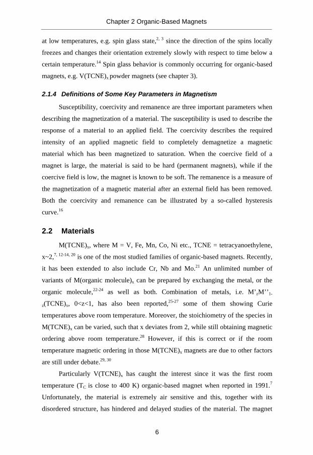
(a) (b)
Figure 2.2 (a) The chemical structure of TCNE. (b) Curie temperatures of different
M(TCNE)x7, 12-14, 26 (the values are approximate and are derived from the powder
form of the materials).
In V(TCNE)x, each vanadium ion is coordinated to six nitrogen atoms most
likely in a slightly distorted octahedral environment. The TCNE molecules are
planar or twisted and can bind to up to four vanadium ions. The local environment is
well-defined with a small distribution of V-N bond lengths, having an average
distance of 2.084(5) Å in room temperature. The strong (covalently) bonded 3D
network explains the insoluble nature of the compound.31
There is an extensive activity in developing new materials for spintronics, but
so far very few show room temperature ordering and semiconducting behavior.32
V(TCNE)x is a semiconductor with a conductivity of about 10-4 Scm-1 at room
temperature. It decreases with decreasing temperature, which suggests a hopping
transport mechanism.33 A low coercive field of about 4.5 Oe has been reported at
room temperature, which is characteristic of a soft magnet.34
The coupling between the 3/2 spin on V2+ and 1/2 spin on the two TCNE-
species is proposed to be antiferromagnetic, yielding a ferrimagnetic state and hence
a net spin of 1/2 for each V(TCNE)2 unit.35 Magnetotransport measurement of
V(TCNE)x thin films have demonstrated positive magnetoresistance,32, 33 i.e.
increase in resistance with applied field. This anomalously large magnetoresistance
M TC (K)V 370Fe 95Mn 75Co 40Ni 40N
NN
N
Chapter 2 Organic-Based Magnets
8
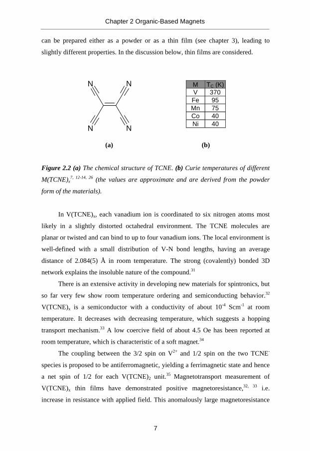
was explained by a model where the �*�band is split into two sub-bands, one
occupied and one unoccupied, with opposite spin polarization. From this model it is
proposed that V(TCNE)x can be described as a fully spin-polarized,
semiconductor.33 No experimental evidence for the proposed valence electronic
structure existed, however. This assumption was later modified after experimentally
showing that the highest occupied molecular orbital (HOMO) actually is V(3d)-
derived (as described above) and hence not TCNE--derived.36 In this modified model
of the ground state of V(TCNE)2, the V(3d) is proposed to split into two orbitals, eg
and t2g, due to crystal field splitting, �, a well-known property of 3d elements. The
HOMO is mainly localized on the V(3d) units and is characterized by strong
hybridization between V(3d) and the TCNE- units.36, 37 The experimental result of
the lowest unoccupied molecular orbital (LUMO) of V(TCNE)x was in agreement
with the one stated above as it is mainly located on the TCNE- units (see Paper I
and Paper II). It is important to note that there may be trap states present,
depending on the preparation method. Those trap states are located below the
TCNE2- level (see Paper II).
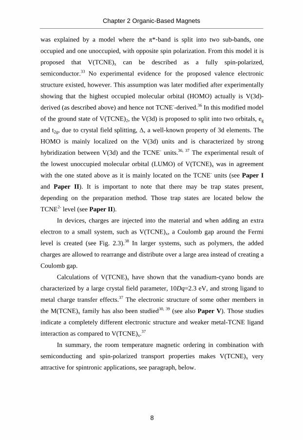
In devices, charges are injected into the material and when adding an extra
electron to a small system, such as V(TCNE)x, a Coulomb gap around the Fermi
level is created (see Fig. 2.3).38 In larger systems, such as polymers, the added
charges are allowed to rearrange and distribute over a large area instead of creating a
Coulomb gap.
Calculations of V(TCNE)x have shown that the vanadium-cyano bonds are
characterized by a large crystal field parameter, 10Dq=2.3 eV, and strong ligand to
metal charge transfer effects.37 The electronic structure of some other members in
the M(TCNE)x family has also been studied30, 39 (see also Paper V). Those studies
indicate a completely different electronic structure and weaker metal-TCNE ligand
interaction as compared to V(TCNE)x.37
In summary, the room temperature magnetic ordering in combination with
semiconducting and spin-polarized transport properties makes V(TCNE)x very
attractive for spintronic applications, see paragraph, below.
Chapter 2 Organic-Based Magnets
9
(TCNE)- V2+
eg
(TCNE)-
π*t2g π*
(TRAP STATE)�
(TCNE)- V2+
eg
(TCNE)-
π*t2g π*
(TRAP STATE)�
(a)
(b)
Figure 2.3 Frontier electronic structure of V(TCNE)2. For more details, see Paper
II (a) Ground state. (b) V(TCNE)x with one extra electron added. Copyright ©
Elsevier B.V.
2.3 Spintronics
In the beginning, organic-based magnets were thought of as replacement of
traditional magnets in generators, motors, transformers etc. More recently it was
shown that they are unlikely to compete with metal magnets.2 Instead, they may find
their own niches since they have exposed properties never associated with magnets
before,2, 4 such as bistability (e.g. light-induced magnetism), transparency, solubility
in organic solvents and potentially biocompatibility. The most promising
applications based on organic-based magnets may be found in the growing field
spintronics.40, 41 Spintronic devices utilize not only the charge of the electron as
information carrier, but also its spin direction. Advantages of using the electron spin
as information carrier include, faster data processing speeds, non-volatility and less
electrical power consumption.41 Examples of (potential) spintronic devices are spin-
V2+(TCNE)2-
eg
(TCNE)-
π*
π*t2g
(TRAP STATE)COULOMB
GAP
V2+(TCNE)2-
eg
(TCNE)-
π*
π*t2g
(TRAP STATE)COULOMB
GAP
Chapter 2 Organic-Based Magnets
10
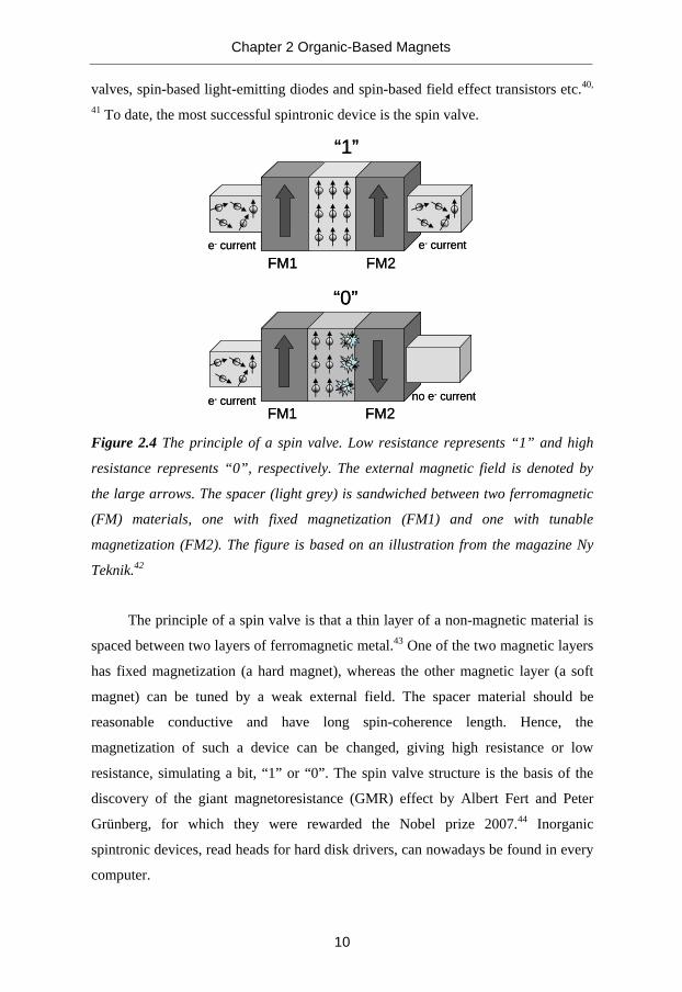
valves, spin-based light-emitting diodes and spin-based field effect transistors etc.40,
41 To date, the most successful spintronic device is the spin valve.
“1”
FM1 FM2e- current e- current
FM1 FM2e- current no e- current
“0”
“1”
FM1 FM2e- current e- current
FM1 FM2e- current no e- current
“0”
Figure 2.4 The principle of a spin valve. Low resistance represents “1” and high
resistance represents “0”, respectively. The external magnetic field is denoted by
the large arrows. The spacer (light grey) is sandwiched between two ferromagnetic
(FM) materials, one with fixed magnetization (FM1) and one with tunable
magnetization (FM2). The figure is based on an illustration from the magazine Ny
Teknik.42
The principle of a spin valve is that a thin layer of a non-magnetic material is
spaced between two layers of ferromagnetic metal.43 One of the two magnetic layers
has fixed magnetization (a hard magnet), whereas the other magnetic layer (a soft
magnet) can be tuned by a weak external field. The spacer material should be
reasonable conductive and have long spin-coherence length. Hence, the
magnetization of such a device can be changed, giving high resistance or low
resistance, simulating a bit, “1” or “0”. The spin valve structure is the basis of the
discovery of the giant magnetoresistance (GMR) effect by Albert Fert and Peter
Grünberg, for which they were rewarded the Nobel prize 2007.44 Inorganic
spintronic devices, read heads for hard disk drivers, can nowadays be found in every
computer.
Chapter 2 Organic-Based Magnets
11
It has been suggested that combining the advantages of spintronics with the
advantages of organic electronics would lead to future’s spintronic devices.11, 45
Organic materials exhibit advantages, such as mechanically flexibility, low
temperature and potential low-cost device fabrication, tunability of the properties via
chemical routes etc.1 In addition, light elements have weak spin-orbit coupling and
low hyperfine interaction, leading to longer spin-coherence times as compared to
inorganic materials.46 The first organic-based spintronic device was presented in
199847 but so far no “all-organic” spintronic device has been reported. Challenges in
the field of organic spintronics include, control and understanding of the transport
mechanism and of the interfaces, development of materials with higher Curie
temperature and higher mobility as well as with increasing sensitivity to weak
magnetic fields.
V(TCNE)x has been proposed to be used in a hybrid spin valve design (see
Fig. 2.4) as the soft magnetic layer.48 In addition, we have recently proposed a new
spin design based on V(TCNE)x where it is sandwiched in between the two
ferromagnetic layers, making use of its fully spin-polarized transport levels (see
Paper IV).

Chapter 2 Organic-Based Magnets
12
�
13
3 Preparation Methods
Fabrication of conventional transition metal and rare earth based magnets
requires high temperature metallurgical synthesis methodologies and is very energy
consuming. Organic-based molecular magnets (OMMs) have the advantage of low-
cost organic synthetic methodologies and together with the concept of “designer
magnets”,49 which refers to that their properties can be tailor-made, make them
attractive in future generations of electronic, magnetic and photonic devices.
However, OMMs have shown to be complicated to prepare and reproduction of the
materials have sometimes shown to be unpredictable.3 Depending on preparation
method, different amounts of disorder are introduced in the material, which can
worsen its properties.34 Hence, it is of high importance with further improvements of
the preparation methods.
In this chapter the development and the preparation routes of the magnets in
the M(TCNE)x family are discussed with focus on preparation of V(TCNE)x.
3.1 Solution-Based Preparation
The first and most frequently used method for preparation of all organic-based
magnets is solution-based organic synthesis preparation. The source materials, the
so-called precursors, are allowed to react in an organic solvent. The solvent can be
either coordinating, which means that the vanadium ions are being blocked by
solvent molecules from binding to the nitrogen of the TCNE molecules or non-
coordinating.34, 50 Both coordinating solvent and non-coordinating solvents introduce
disorder in the material. However, whereas the coordinating solvent substantially
influence the Curie temperature, the non-coordinating does not but can lead to e.g.
spin-glass behavior at low temperatures.50 For preparation of V(TCNE)x, the
precursors are TCNE and bis(benzene)vanadium,7 V(C6H6)2, or vanadium
Chapter 3 Preparation Methods
14
hexacarbonyl,34 V(CO)6. When the reaction has taken place in the organic solvent,
the resulting precipitate is filtrated and dried under vacuum, forming an amorphous
insoluble magnetic powder.51 Magnets prepared by this method always contain
residual solvent molecules and residual precursors or by-products thereof. As
described above, this causes disorder in the material and V(TCNE)x prepared by
chemical synthesis is extremely air sensitive and decomposes after only a few
seconds in air, sometimes in a pyrophoric manner.7
3.2 Chemical Vapor Deposition (CVD)
Chemical vapor deposition (CVD)21, 52, 53 is commonly used in e.g. the
semiconductor industry to produce thin films. The precursors are provided in
gaseous form and transported (often diluted in a carrier gas) into the chamber where
the chemical reaction takes place on or in near vicinity of a substrate. The main
drawback of CVD processes is the use of often toxic, corrosive and/or flammable
precursors. Frequently, not only the desired material, but also by-products are
formed upon the reaction. There are many different types of CVD systems,
depending on operating pressures and/or temperatures etc. The low temperature
processing of organic materials allow the growth of organic-based magnets on
polymer or even paper substrates, enabling production of all-organic devices.21
Processing of V(TCNE)x by chemical vapor deposition (CVD) was the first
step towards applications since the method produces thin films.54, 55 As these thin
films are solvent-free, the detrimental effect of the solvent is eliminated, resulting in
enhanced air stability and magnetic properties of the magnets, as compared to the
chemically synthesized ones.55 Apart from V(TCNE)x, also M(TCNE)x, where M =
Cr, Nb and Mo have been prepared by the CVD-based technique.21 Similar to the
chemically synthesized magnets, the thin film magnets produced by this CVD-based
method contains substantial amounts of oxygen.55 Therefore has our research group
developed an in situ ultra-high vacuum (UHV) compatible CVD method,36, 37
leading to preparation of the first completely oxygen-free V(TCNE)x thin films. In
this process, V(C6H6)2, and TCNE are allowed to react in the vacuum chamber and
no carrier gas is used to transport the precursors. Hence, this in situ preparation
allows for usage of more sophisticated surface-sensitive methods for
Chapter 3 Preparation Methods
15
characterization of e.g. the electronic structure and the magnetic properties of the
materials. As mentioned above, by the use of CVD the negative effect of residual
solvents is eliminated, but also thin films prepared by this method contain residual
precursors and/or by-products from the gas-phase reaction. The UHV compatible
CVD method was used for preparation of V(TCNE)x in Paper I and Paper II.
SUBSTRATEADSORPTION
GAS FLOW GAS PHASE REACTION
TRANSPORT OF BY-PRODUCTS
SURFACE DIFFUSION
TRANSPORT TO SURFACE
DESORPTION
SUBSTRATEADSORPTION
GAS FLOW GAS PHASE REACTION
TRANSPORT OF BY-PRODUCTS
SURFACE DIFFUSION
TRANSPORT TO SURFACE
DESORPTION
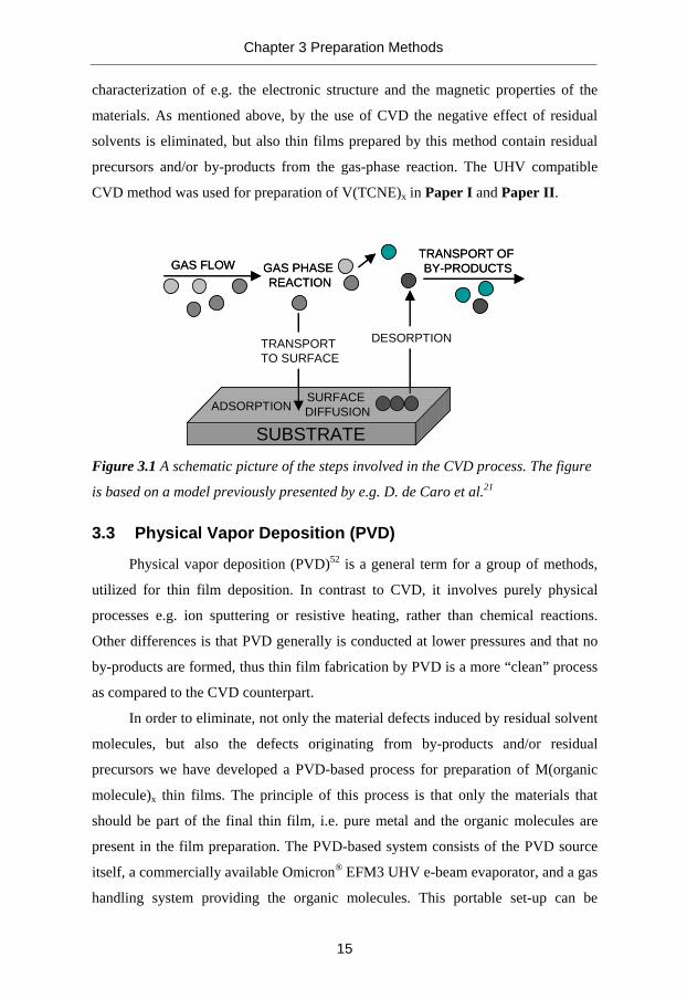
Figure 3.1 A schematic picture of the steps involved in the CVD process. The figure
is based on a model previously presented by e.g. D. de Caro et al.21
3.3 Physical Vapor Deposition (PVD)
Physical vapor deposition (PVD)52 is a general term for a group of methods,
utilized for thin film deposition. In contrast to CVD, it involves purely physical
processes e.g. ion sputtering or resistive heating, rather than chemical reactions.
Other differences is that PVD generally is conducted at lower pressures and that no
by-products are formed, thus thin film fabrication by PVD is a more “clean” process
as compared to the CVD counterpart.
In order to eliminate, not only the material defects induced by residual solvent
molecules, but also the defects originating from by-products and/or residual
precursors we have developed a PVD-based process for preparation of M(organic
molecule)x thin films. The principle of this process is that only the materials that
should be part of the final thin film, i.e. pure metal and the organic molecules are
present in the film preparation. The PVD-based system consists of the PVD source
itself, a commercially available Omicron® EFM3 UHV e-beam evaporator, and a gas
handling system providing the organic molecules. This portable set-up can be
Chapter 3 Preparation Methods
16
mounted on any (ultra-high) vacuum system, allowing for in situ preparation and
characterization of the thin film magnets.
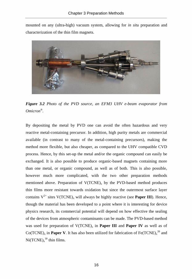
Figure 3.2 Photo of the PVD source, an EFM3 UHV e-beam evaporator from
Omicron®.
By depositing the metal by PVD one can avoid the often hazardous and very
reactive metal-containing precursor. In addition, high purity metals are commercial
available (in contrast to many of the metal-containing precursors), making the
method more flexible, but also cheaper, as compared to the UHV compatible CVD
process. Hence, by this set-up the metal and/or the organic compound can easily be
exchanged. It is also possible to produce organic-based magnets containing more
than one metal, or organic compound, as well as of both. This is also possible,
however much more complicated, with the two other preparation methods
mentioned above. Preparation of V(TCNE)x by the PVD-based method produces
thin films more resistant towards oxidation but since the outermost surface layer
contains V2+ sites V(TCNE)x will always be highly reactive (see Paper III). Hence,
though the material has been developed to a point where it is interesting for device
physics research, its commercial potential will depend on how effective the sealing
of the devices from atmospheric contaminants can be made. The PVD-based method
was used for preparation of V(TCNE)x in Paper III and Paper IV as well as of
Co(TCNE)x in Paper V. It has also been utilized for fabrication of Fe(TCNE)x39 and
Ni(TCNE)x30 thin films.
�
17
4 Experimental Techniques
All the research presented in this thesis is based on different types of
photoelectron spectroscopy (PES) and near edge X-ray absorption fine structure
(NEXAFS) spectroscopy. Those techniques are well suited for studies of the
surfaces and interfaces of thin film organic-based magnets. Magnetic
characterization of the samples can be performed (among others) by a
superconducting quantum interference device (SQUID) magnetometer.
4.1 Photoelectron Spectroscopy
Photoelectron spectroscopy (PES) is a very surface sensitive method which
can be used for studies of solids, gases or even liquids.56, 57 The technique is also
known as ESCA,58 electron spectroscopy for chemical analysis. It is based on the
photoelectric effect which was discovered by Hertz in 1887 and explained
theoretically by Einstein in 1905.59 The large interest in the method began in the
1960s when high-resolution spectrometers were developed by K. Siegbahn and co-
workers in Uppsala, Sweden.60 Photoelectron spectroscopy is often referred to as a
fingerprint technique since each element has its unique PES pattern and all elements
except hydrogen can be detected and studied. In addition, many chemical and
physical properties of a sample can be obtained by the technique.56, 59
4.1.1 The Principle of Photoionization
When a sample is illuminated with photons (e.g. X-rays, UV-light or
synchrotron radiation) of known, high enough energy, photoelectrons may be
emitted. This is called photoionization or the photoelectric effect.59 The ejected
photoelectrons are collected and detected by a system comprising of electrostatic
lenses, an (hemispherical) analyzer, an electron multiplier and a detector. The
emitted electrons are analyzed with respect to their kinetic energy, Ekin, and since the
Chapter 4 Experimental Techniques
18
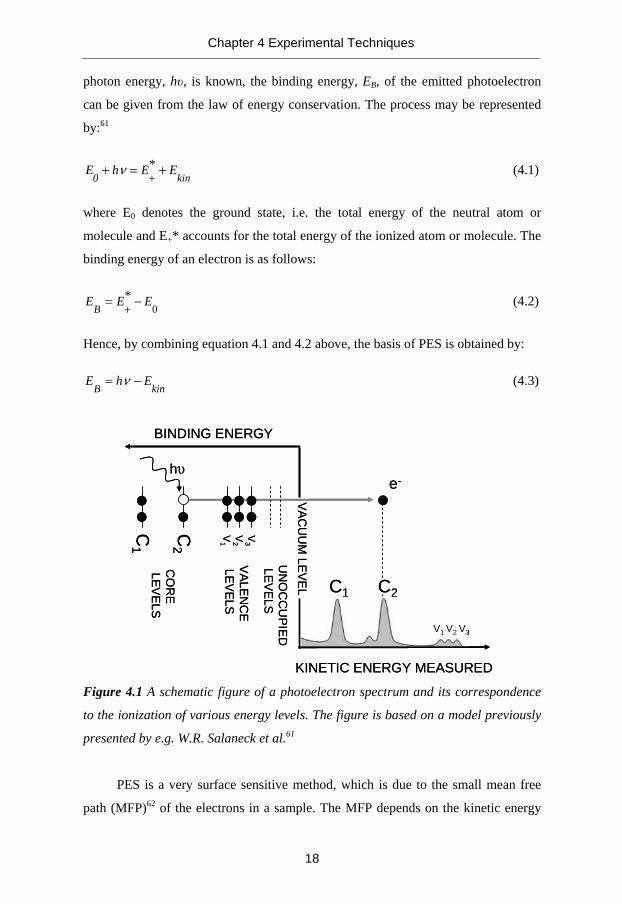
photon energy, h�, is known, the binding energy, EB, of the emitted photoelectron
can be given from the law of energy conservation. The process may be represented
by:61
kin0E*EhE +=+
+ν (4.1)
where E0 denotes the ground state, i.e. the total energy of the neutral atom or
molecule and E+* accounts for the total energy of the ionized atom or molecule. The
binding energy of an electron is as follows:
0* EEE
B−=
+(4.2)
Hence, by combining equation 4.1 and 4.2 above, the basis of PES is obtained by:
kinBEhE −= ν (4.3)
KINETIC ENERGY MEASURED
BINDING ENERGY
UN
OC
CU
PIEDLE
VE
LS
VALEN
CE
LEV
ELS
CO
RE
LEV
ELS
VACU
UM
LEVEL
C1
C2
V3
V2
V1
e-
C1
V1 V2 V3
C2
h�
KINETIC ENERGY MEASURED
BINDING ENERGY
UN
OC
CU
PIEDLE
VE
LS
VALEN
CE
LEV
ELS
CO
RE
LEV
ELS
VACU
UM
LEVEL
C1
C2
V3
V2
V1
e-
C1
V1 V2 V3
C2
h�
Figure 4.1 A schematic figure of a photoelectron spectrum and its correspondence
to the ionization of various energy levels. The figure is based on a model previously
presented by e.g. W.R. Salaneck et al.61
PES is a very surface sensitive method, which is due to the small mean free
path (MFP)62 of the electrons in a sample. The MFP depends on the kinetic energy
Chapter 4 Experimental Techniques
19
of the electrons and determines the depth from which the electrons can escape
undisturbed (i.e. without loosing energy). The MFP is best illustrated by the so-
called universal curve.62 Electrons emancipating from larger distances than the MFP
are called secondary electrons and give rise to background in the PES spectra (or
remain in the sample), complicating the analysis of a sample.59
X-ray photoelectron spectroscopy (XPS), which is used for core level studies,
gives a surface sensitivity of approximately 100 Å for electrons of high kinetic
energy (Ekin>1000 eV). The valence levels can be studied by ultra-violet
photoelectron spectroscopy (UPS) which is even more surface sensitive with only
the first few monolayers (~ 15-20 Å) contributing to the signal. In order to be able to
detect the electrons escaping from the surface, the MFP of the electrons needs to be
longer than the distance between the sample surface and the detector. This requires
high vacuum conditions (~ 10-6 mbar).63 Besides, to keep the surface free from
contaminations during the measurement of a reactive surface, the pressure should be
below 10-9 mbar, i.e. in the ultra-high vacuum region.63
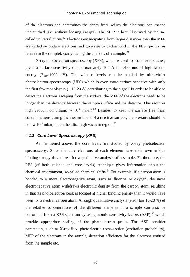
4.1.2 Core Level Spectroscopy (XPS)
As mentioned above, the core levels are studied by X-ray photoelectron
spectroscopy. Since the core electrons of each element have their own unique
binding energy this allows for a qualitative analysis of a sample. Furthermore, the
PES (of both valence and core levels) technique gives information about the
chemical environment, so-called chemical shifts.64 For example, if a carbon atom is
bonded to a more electronegative atom, such as fluorine or oxygen, the more
electronegative atom withdraws electronic density from the carbon atom, resulting
in that its photoelectron peak is located at higher binding energy than it would have
been for a neutral carbon atom. A rough quantitative analysis (error bar 10-20 %) of
the relative concentrations of the different elements in a sample can also be
performed from a XPS spectrum by using atomic sensitivity factors (ASF),56 which
provide appropriate scaling of the photoelectron peaks. The ASF consider
parameters, such as X-ray flux, photoelectric cross-section (excitation probability),
MFP of the electrons in the sample, detection efficiency for the electrons emitted
from the sample etc.
Chapter 4 Experimental Techniques
20
From the photoelectron peaks the thickness of a thin film onto a substrate can
be estimated by the attenuation of the substrate signal after the thin film has been
deposited:63
���
��� −=�d
expII 0 (4.4)
where d is the film thickness, I0 is the original signal, I is the attenuated signal and �
is the MFP.
h� h�
UNOCCUPIED LEVELS
CORE LEVELS
PHOTO-IONIZATION
VALENCE LEVELS
SHAKE-UP
SHAKE-OFF
AUGER EMISSION
h�h� h�
UNOCCUPIED LEVELS
CORE LEVELS
PHOTO-IONIZATION
VALENCE LEVELS
SHAKE-UP
SHAKE-OFF
AUGER EMISSION
h�
Figure 4.2 A schematic figure of some possible electron emitting processes, namely
photoionization (from a core level), shake-up, shake-off and Auger emission. The
figure illustrates well-known concepts previously shown by e.g. W.R. Salaneck et
al.61
Apart from photoelectron peaks which are the most narrow and intense peaks in a
PES spectrum, there may be many other features, resulting from more complex and
usually less probable final states. This is due to that the electronic structure of an
atom or molecule has time to relax after a photoionization event. Different screening
effects give rise to different excited states (each with its own probability). Fig. 4.2
illustrates examples of some possible electron emitting processes, namely
photoionization, shake-up, shake-off and Auger emission.65 Both shake-ups and
shake-offs are located at higher binding energies than the photoelectron peak, due to
Chapter 4 Experimental Techniques
21
energy losses. Shake-ups can be used when studying the frontier unoccupied
electronic structure (see e.g. Paper II).
4.1.3 Valence Level Spectroscopy (UPS)
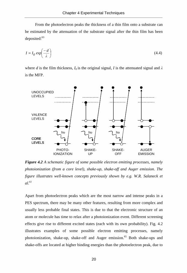
Using ultraviolet light as excitation source was demonstrated in the 1960s,66
shortly after the development of XPS. The technique, depicted as ultraviolet
photoelectron spectroscopy (UPS), is commonly used for studies of the density of
occupied electronic states in the valence band. A UPS spectrum also provides
information needed for determination of some important parameters of a sample,
such as the ionization potential or work function.61
SE
CO
ND
AR
Y e-
CU
T-O
FF
FER
MI L
EV
EL
VA
CU
UM
LE
VEL
ECO EF=0 Evac
h�s
BINDING ENERGY (eV)
INTE
NSI
TY (a
rb. u
nits
)
SE
CO
ND
AR
Y e-
CU
T-O
FF
FER
MI L
EV
EL
VA
CU
UM
LE
VEL
ECO EF=0 Evac
h�ss
BINDING ENERGY (eV)
INTE
NSI
TY (a
rb. u
nits
)
Figure 4.3 A HeI spectrum of gold pointing out some of the information that can be
obtained from UPS. See e.g. W.R. Salaneck et al.61
The work function, sφ , can be derived from:
COFvac Eh�EEs −=−=φ (4.5)
where Evac is the vacuum level energy, EF is the Fermi level energy, h� is the photon
energy and ECO is the cut-off energy of the secondary electrons.61
UPS is a suitable technique for e.g. studies of work function and valence
feature changes upon the early stages of doping (for this purpose UPS was used in
Paper I and Paper II, even not shown in the papers).
Chapter 4 Experimental Techniques
22
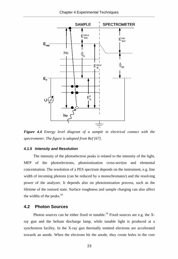
4.1.4 Reference Level
The binding energy scale of a PES spectrum must be defined with respect to a
reference. In contrast to gas phase samples where the vacuum level is the natural
reference level, the reference level of a solid sample is more complicated. If the
sample is in electrical contact with the spectrometer, the Fermi level of the sample
and the spectrometer align and the binding energy is measured relative the Fermi
level.63 The photoionization equation for a solid sample can hence be written:56
spkinFB EEh� φ++= (4.6)
where FBE is the binding energy relative the Fermi energy, kinE is the kinetic
energy of the photoelectrons and spφ is the work function of the spectrometer.
If the sample is poorly conducting the assumption that the sample and
spectrometer Fermi level is common is not valid. Positive charges will be
accumulated in the sample, leading to that the features in a photoelectron
spectroscopy spectrum will appear at higher binding energy than expected.
Compensation can be done by an electron flood gun,63 which ensures electrical
neutrality at the surface of the sample.
Sometimes, when work function changes are studied, e.g. upon doping, the
vacuum level is used as reference point (see e.g. Paper II). If the work function of
the sample is known, it enables the adjustment of the binding energy (by adding the
work function to the peaks) so that the vacuum level can be used as reference.
Chapter 4 Experimental Techniques
23
EF
SAMPLE SPECTROMETER
h�
U
Evac
Evac*kin Evackin
EFB
Evac*B
h�
s
sp
EF
SAMPLE SPECTROMETER
h�
U
Evac
Evac*kinEvac*kin EvackinEvackin
EFB
Evac*BEvac*B
h�
ss
spsp
Figure 4.4 Energy level diagram of a sample in electrical contact with the
spectrometer. The figure is adopted from Ref [67].
4.1.5 Intensity and Resolution
The intensity of the photoelectron peaks is related to the intensity of the light,
MFP of the photoelectrons, photoionization cross-section and elemental
concentration. The resolution of a PES spectrum depends on the instrument, e.g. line
width of incoming photons (can be reduced by a monochromator) and the resolving
power of the analyzer. It depends also on photoionization process, such as the
lifetime of the ionized state. Surface roughness and sample charging can also affect
the widths of the peaks.59
4.2 Photon Sources
Photon sources can be either fixed or tunable.59 Fixed sources are e.g. the X-
ray gun and the helium discharge lamp, while tunable light is produced at a
synchrotron facility. In the X-ray gun thermally emitted electrons are accelerated
towards an anode. When the electrons hit the anode, they create holes in the core
Chapter 4 Experimental Techniques
24
shells of the anode material, resulting in de-excitations from higher energy levels
and hence emission of X-ray radiation. The most commonly used anodes are
aluminum or magnesium, producing X-rays of AlK� = 1486.6 eV and MgK� =
1253.6 eV, respectively. A helium discharge lamp contains helium gas kept in an
enclosure and when applying an electric field the gas becomes ionized. Upon
relaxation of the ionized (excited) atoms in the gas, photons of HeI = 21.2 eV or
HeII = 40.8 eV are emitted.59
Synchrotron radiation is produced by circulating charged particles, usually
electrons, in an ultra high vacuum storage ring at relativistic speeds, i.e. close to that
of light. When the charges are accelerated by bending magnets or insertion devices,
such as wigglers or undulators,68 they emit electromagnetic radiation. The energy of
the synchrotron light typically covers a large range of the energy spectrum, ranging
from infrared (IR) to hard X-rays and by using a monochromator the energy of the
light can be tuned to suit a specific experiment, such as PES or absorption
spectroscopy (discussed below). Other characteristics of synchrotron radiation
include high photon flux, brilliance (or brightness) and polarized light.69 Several
beamlines are attached to the storage ring and each of them is dedicated to one or a
few specific techniques. The development of synchrotron radiation started in the
1940s and today there are about 40 facilities in the world of which one, MAX-lab70
(where the experiments in this thesis were performed) is located in Lund, Sweden.69
4.3 Absorption Spectroscopy
Near edge X-ray absorption fine structure (NEXAFS) spectroscopy is a
method for studying the frontier unoccupied electronic states in presence of a core
hole.71 The region studied by NEXAFS is the actual absorption edge (onset) and
about 30 eV above it. There are two different ways of performing the measurements,
i.e. transmission or photoyield mode. In the transmission mode the X-rays that are
transmitted through the sample are measured. This mode has limited use since it
requires thick and free-standing films. The photoyield mode measures the absorption
in a more indirect way, by studying the decay products. The decay products relates
to emitted electrons (electron yield) or fluorescent photons (fluorescent yield) which
are produced when an excited atom relax. The electron yield is most suitable for
Chapter 4 Experimental Techniques
25
light elements and therefore it appears as the best alternative for studies of organic
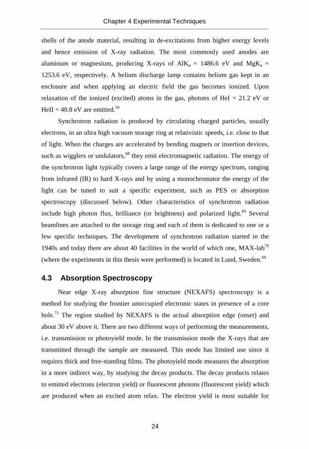
materials. In the electron yield, absorption of photons is followed by excitation of
core electrons to originally (bound) unoccupied states. Those states decay and
therefore an absorption event is followed by a dramatically increase of the number
emitted electrons. The absorption and the possible decay channels are illustrated in
Fig. 4.5.
h�
UNOCCUPIED LEVELS
CORE LEVELS
ABSORPTION
VALENCE LEVELS
SPECTATOR DECAY
PARTICIPATOR DECAY
h�
UNOCCUPIED LEVELS
CORE LEVELS
ABSORPTION
VALENCE LEVELS
SPECTATOR DECAY
PARTICIPATOR DECAY
Figure 4.5 Principle of absorption and the following Auger processes (decay
channels). See e.g. N. Mårtensson et al.72
Furthermore, the electron yield can be performed in two different ways, namely total
yield and partial yield.71 In total yield are all electrons counted, both Auger electrons
and photoelectrons. In partial yield only the Auger electrons are counted, leading to
a more surface sensitive analysis than the total electron yield mode. Since the energy
must be swept across the onset energy, NEXAFS implies the use of a tunable photon
source. As core levels are involved in the process, NEXAFS is an elemental specific
technique and can provide information regarding both the elemental composition as
well as the local chemical environment. For example, the technique can be a useful
tool for determining the nature of the frontier unoccupied electronic structure (see
e.g. Paper I, Paper II). NEXAFS can also be used for studying the orientation of
Chapter 4 Experimental Techniques
26
the molecules by measuring the sample at different rotations (relative to the
analyzer).71
4.4 Resonant Photoelectron Spectroscopy (RPES)
Similar to absorption spectroscopy the decay products after an absorption
event are studied in resonant photoelectron spectroscopy (RPES).72 However, in
RPES it is the binding energy of the decay products versus the electron yield that are
considered. The experiment is performed by sweeping the photon energy in discrete
steps over a specific absorption edge while monitoring the electrons emitted from
the valence region. The lifetime of a core-excited state is on the femtosecond scale
and when it decays it can do so in different ways as shown in Fig. 4.5. For the non-
radiative emission there are two Auger decay channels, participator and spectator
decay, respectively, and for RPES the participator decay is of main interest. The
participator and spectator decays can be distinguished by their energy dispersions,
for participator decay the peaks appear at constant binding energy while the binding
energy of spectator decay depends linearly on the photon energy. In participator
decay the final states are energetically the same as for the valence PES, i.e. one
valence hole, however the transition matrix elements are different, namely dipole for
PES and Coulomb for RPES. For the spectator decay the final state is more complex
with two holes and one electron.72
Since core excitations are site-specific, RPES allows for determination of the
origin of certain valence features and e.g. the origin of the HOMO of a compound
(see e.g. Paper V). RPES can also be used for charge transfer dynamics studies,72
mainly for small systems since a detailed interpretation of RPES spectra requires
complex theoretical calculations.
4.5 Superconducting Quantum Interference Device (SQUID)
A superconducting quantum interference device (SQUID) magnetometer is
based on the Josephson effect of superconductors and can detect extremely weak
magnetic fields (even those produced by brain activity).73 The Josephson effect
occurs when current flows across two superconducting materials which are
separated my a thin isolating layer.73 This set-up is known as a Josephson junction.
A SQUID consists of a superconducting ring containing two Josephson junctions
Chapter 4 Experimental Techniques
27
and the Josephson effect appears when a sample is passed through the ring. The
induced current is proportional to the magnetization of the sample.74, 75 A SQUID
measures the quantitative magnetization and the data can be used to e.g. determine
the Curie temperature or the magnetic moment of atoms in a sample. The
magnetization is measured either as a function of temperature in a constant magnetic
field or as a function of applied magnetic field at constant temperature. The SQUID
method was used by our collaborators in Uppsala for obtaining some of the data in
Paper III.

Chapter 4 Experimental Techniques
28

�
29
5 Equipment
The work presented in this thesis has been performed at the two photoelectron
spectrometers “Scienta” and “Moses” in the laboratories of Surface Physics and
Chemistry Division at Linköping University. Additional measurements that required
a tunable photon source were performed at beamline I311 and D1011 at the Swedish
national synchrotron laboratory, MAX-lab70 in Lund, Sweden.
5.1 Moses
Moses is a custom-built photoelectron spectrometer for X-ray and ultraviolet
photoelectron spectroscopy (XPS and UPS). The system consists of a hemispherical
analyzer and an electron detector. It has three vacuum chambers namely,
introduction, preparation and analysis chamber. The analysis chamber is equipped
with a non-monochromatized X-ray source (h�: AlK� = 1486.6 eV) and a
monochromatized helium discharge lamp (h�: HeI = 21.2 eV and HeII = 40.8 eV).
The preparation chamber allows for in situ sample preparation and is equipped with
an ion sputter gun, a gas handling system (for sample preparation from gas- or vapor
phase) and possibilities to mount deposition sources. The sample temperature can be
controlled in the range -190 °C by liquid nitrogen, up to 300 °C by resistive heating.
The base pressure is better than 1·10-9 mbar and obtained by a combination of turbo
molecular, ion getter and cryogenic pumps. Parts of the work presented in Paper I
and Paper II were performed in Moses.
Chapter 5 Equipment
30
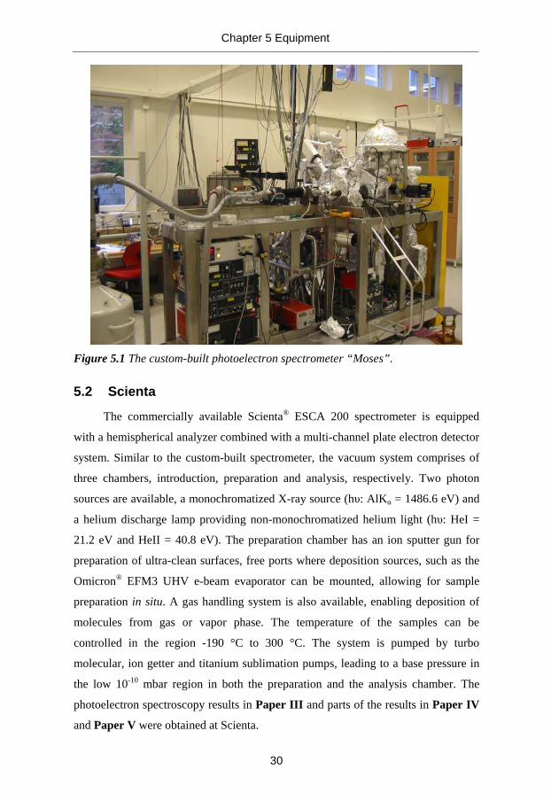
Figure 5.1 The custom-built photoelectron spectrometer “Moses”.
5.2 Scienta
The commercially available Scienta® ESCA 200 spectrometer is equipped
with a hemispherical analyzer combined with a multi-channel plate electron detector
system. Similar to the custom-built spectrometer, the vacuum system comprises of
three chambers, introduction, preparation and analysis, respectively. Two photon
sources are available, a monochromatized X-ray source (h�: AlK� = 1486.6 eV) and
a helium discharge lamp providing non-monochromatized helium light (h�: HeI =
21.2 eV and HeII = 40.8 eV). The preparation chamber has an ion sputter gun for
preparation of ultra-clean surfaces, free ports where deposition sources, such as the
Omicron® EFM3 UHV e-beam evaporator can be mounted, allowing for sample
preparation in situ. A gas handling system is also available, enabling deposition of
molecules from gas or vapor phase. The temperature of the samples can be
controlled in the region -190 °C to 300 °C. The system is pumped by turbo
molecular, ion getter and titanium sublimation pumps, leading to a base pressure in
the low 10-10 mbar region in both the preparation and the analysis chamber. The
photoelectron spectroscopy results in Paper III and parts of the results in Paper IV
and Paper V were obtained at Scienta.
Chapter 5 Equipment
31
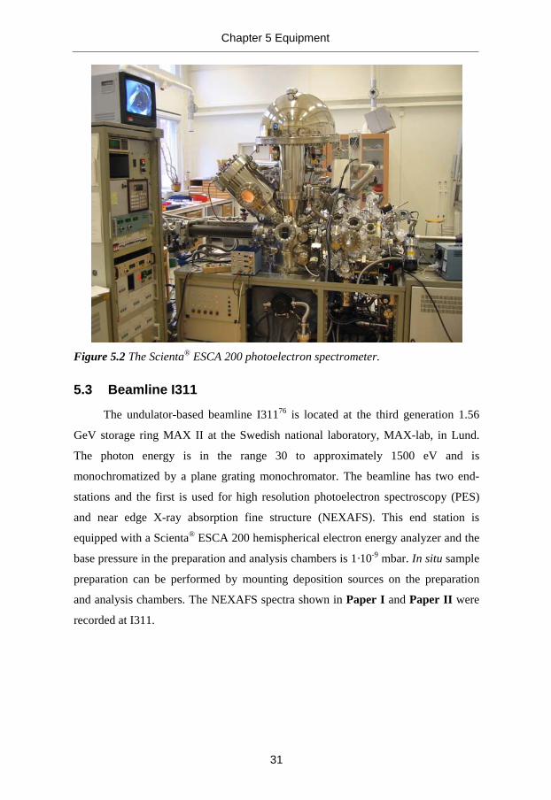
Figure 5.2 The Scienta® ESCA 200 photoelectron spectrometer.
5.3 Beamline I311
The undulator-based beamline I31176 is located at the third generation 1.56
GeV storage ring MAX II at the Swedish national laboratory, MAX-lab, in Lund.
The photon energy is in the range 30 to approximately 1500 eV and is
monochromatized by a plane grating monochromator. The beamline has two end-
stations and the first is used for high resolution photoelectron spectroscopy (PES)
and near edge X-ray absorption fine structure (NEXAFS). This end station is
equipped with a Scienta® ESCA 200 hemispherical electron energy analyzer and the
base pressure in the preparation and analysis chambers is 1·10-9 mbar. In situ sample
preparation can be performed by mounting deposition sources on the preparation
and analysis chambers. The NEXAFS spectra shown in Paper I and Paper II were
recorded at I311.
Chapter 5 Equipment
32
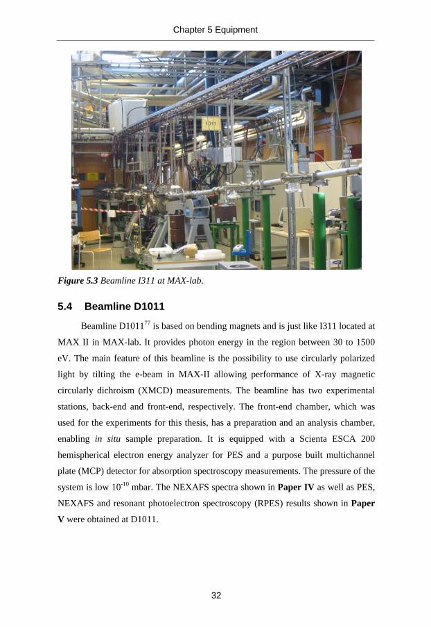
Figure 5.3 Beamline I311 at MAX-lab.
5.4 Beamline D1011
Beamline D101177 is based on bending magnets and is just like I311 located at
MAX II in MAX-lab. It provides photon energy in the region between 30 to 1500
eV. The main feature of this beamline is the possibility to use circularly polarized
light by tilting the e-beam in MAX-II allowing performance of X-ray magnetic
circularly dichroism (XMCD) measurements. The beamline has two experimental
stations, back-end and front-end, respectively. The front-end chamber, which was
used for the experiments for this thesis, has a preparation and an analysis chamber,
enabling in situ sample preparation. It is equipped with a Scienta ESCA 200
hemispherical electron energy analyzer for PES and a purpose built multichannel
plate (MCP) detector for absorption spectroscopy measurements. The pressure of the
system is low 10-10 mbar. The NEXAFS spectra shown in Paper IV as well as PES,
NEXAFS and resonant photoelectron spectroscopy (RPES) results shown in Paper
V were obtained at D1011.
�
Chapter 5 Equipment
33
�
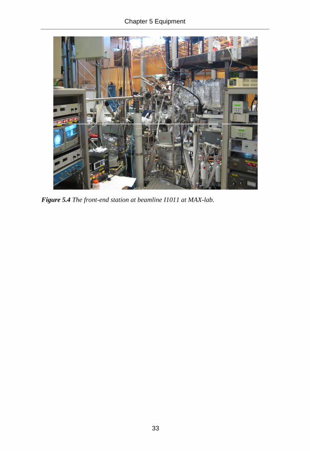
Figure 5.4 The front-end station at beamline I1011 at MAX-lab. �

Chapter 5 Equipment
34
�
35
6 Summary and Future Outlook
In this last chapter a review of the work presented in the thesis is provided.
The two last paragraphs also contain a short discussion about our current work and a
future outlook.
6.1 Background
As the organic-based magnet vanadium tetracyanoethylene, V(TCNE)x, is an
attractive material for spintronics devices, knowledge about its electronic and
chemical structure as well as its interface with ferromagnetic (FM) metals are of
high importance. Surface studies by different photoelectron and absorption
spectroscopy techniques are well suited for this purpose and were therefore utilized
for the work presented in the thesis. However, the material was first prepared as
powder7 and later as ex situ prepared thin films,54, 55 of which both are extremely air
sensitive. Therefore these very surface-sensitive measurement techniques were not
feasible and hence the electronic structure of the material remained unknown for
long time. In our research group the work about organic-based magnets started with
experimental and theoretical studies of a model compound of V(TCNE)x, namely
Rb-doped TCNE,38 which provided information about the nature of the charge
carriers and some insight into the magnetic properties of V(TCNE)x. The next step
was development of a new in situ preparation method of V(TCNE)x by an ultra-high
vacuum (UHV) compatible process based on chemical vapor deposition (CVD),
resulting in completely oxygen-free thin films.36 This in situ method enabled for the
first time measurements by sophisticated surface analysis methods such as
photoelectron spectroscopy and absorption spectroscopy.
�
Chapter 6 Summary and Future Outlook
36
6.2 Summary of the Thesis
To be able to correct understand the (spin-polarized) injection and transport
properties of V(TCNE)x, the accepting and transporting levels of electrons and holes
of the material must be known. A model of the electronic structure of V(TCNE)x
was suggested by Prigodin et al, but without being confirmed experimentally.33 In
this model, both the highest occupied molecular orbital (HOMO) and the lowest
unoccupied molecular orbital (LUMO) of the material was proposed to be TCNE-
derived. The model was later modified by experimental resonant photoelectron
spectroscopy (RPES) results of the frontier occupied electronic structure performed
by our research group36 since it was shown that the HOMO of V(TCNE)x is actually
mainly derived from V(3d) and not only from TCNE. However, no experimental
results of the frontier unoccupied electronic structure existed at this time. Therefore,
the purpose of Paper I was to gain information about the frontier unoccupied
electronic structure of V(TCNE)x. With this intention, V(TCNE)x, Na-doped TCNE
and pristine TCNE were studied by X-ray and UV photoelectron spectroscopy (XPS
and UPS) as well as with near edge X-ray absorption fine structure (NEXAFS)
spectroscopy. Na-doped TCNE can act as model system of V(TCNE)x since Na n-
dopes TCNE but has the advantage that it is less complex than V(TCNE)x. The
spectra of the two compounds are quite similar with the main exception that the
V(TCNE)x peaks are slightly broader which can be attributed to structural disorder
of V(TCNE)x. The experimental results were interpreted together with theoretical
calculations of the NEXAFS spectra of pristine TCNE as well as of Na-doped
TCNE. The calculations were performed by our collaborators at KTH in Stockholm.
By comparing the experimental and theoretical results of pristine TCNE, the
contributions from the various carbon species (cyano and vinyl) could be
disentangled. In contrast to the occupied electronic structure,36, 37 which is strongly
hybridized, this study showed that there is no (or very little) hybridization between
vanadium and TCNE in the unoccupied frontier electronic structure, which means
that the LUMO is either localized on vanadium or on TCNE.
Chapter 6 Summary and Future Outlook
37
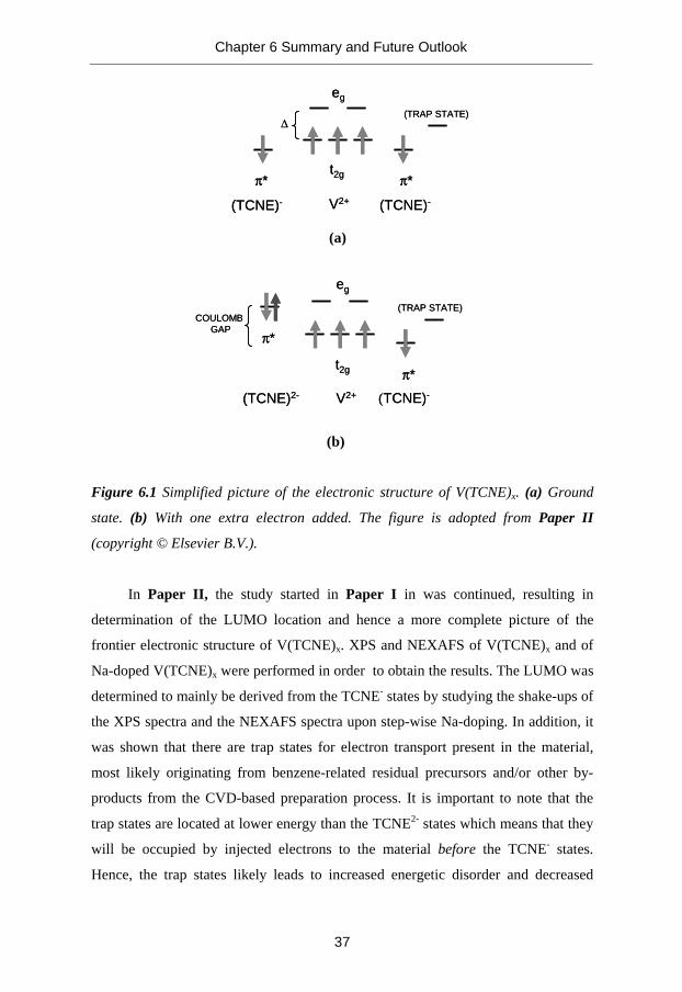
(TCNE)- V2+
eg
(TCNE)-
π*t2g π*
(TRAP STATE)�
(TCNE)- V2+
eg
(TCNE)-
π*t2g π*
(TRAP STATE)�
(a)
(b)
Figure 6.1 Simplified picture of the electronic structure of V(TCNE)x. (a) Ground
state. (b) With one extra electron added. The figure is adopted from Paper II
(copyright © Elsevier B.V.).
In Paper II, the study started in Paper I in was continued, resulting in
determination of the LUMO location and hence a more complete picture of the
frontier electronic structure of V(TCNE)x. XPS and NEXAFS of V(TCNE)x and of
Na-doped V(TCNE)x were performed in order to obtain the results. The LUMO was
determined to mainly be derived from the TCNE- states by studying the shake-ups of
the XPS spectra and the NEXAFS spectra upon step-wise Na-doping. In addition, it
was shown that there are trap states for electron transport present in the material,
most likely originating from benzene-related residual precursors and/or other by-
products from the CVD-based preparation process. It is important to note that the
trap states are located at lower energy than the TCNE2- states which means that they
will be occupied by injected electrons to the material before the TCNE- states.
Hence, the trap states likely leads to increased energetic disorder and decreased
V2+(TCNE)2-
eg
(TCNE)-
π*
π*t2g
(TRAP STATE)COULOMB
GAP
V2+(TCNE)2-
eg
(TCNE)-
π*
π*t2g
(TRAP STATE)COULOMB
GAP
Chapter 6 Summary and Future Outlook
38
mobility of the material. The results obtained from Paper I and Paper II have
strong implication on the design of devices based on V(TCNE)x, as the frontier
electronic structure is highly important for its charge transport and magnetic
properties.
As shown by Paper II, (benzene-related) impurities induce disorder in the
material and can work as trap states for electron transport. The impurities may also
function as oxygen-reaction sites. Hence, it would be desirable (or even necessary)
to develop organic-based magnets without this type of impurities. In Paper III a
new preparation method, based on physical vapor deposition (PVD), of hybrid
organic-based magnets is presented. The principle of this method is that no other
materials than the ones that should be part of the final films is present in the
preparation process, i.e. only pure vanadium and TCNE in the case of V(TCNE)x
preparation. This would lead to a less disordered material since it lacks
contamination from residual precursors and/or by-products thereof. Just like the
CVD process reported by our group the thin films of V(TCNE)x prepared by the
PVD-based process is prepared under UHV conditions and are completely free from
oxygen. The thin films of V(TCNE)x were studied by XPS, UPS and compared with
results of V(TCNE)x prepared by CVD. The magnetic characterization was
performed with a superconducting quantum interference device (SQUID) by
collaborators in Uppsala. The first study of V(TCNE)x prepared by this technique
showed that those films are more resistant towards oxygen as compared to
previously reported CVD-prepared thin films. However, it is important to note that
the outermost surface of V(TCNE)x always will be highly reactive due to the V2+
sites present. The first result on the critical temperature of V(TCNE)x prepared by
this method is in very well agreement (TC~365 K) with previously shown values of
V(TCNE)x, both for thin films and powders.7, 34 Furthermore, the method is much
more flexible since pure metal is used instead of the often hazardous and not always
commercially available precursors. This method also easily enables preparation of
other members of the M(TCNE)x family as well as M’M’’(TCNE)x (with two or
even up to three metals), see Paper III. So far this preparation method has been
used for preparation of Fe(TCNE)x,39 Ni(TCNE)x
30 and Co(TCNE)x (see Paper V).
Chapter 6 Summary and Future Outlook
39
FM
FM
”ON” ”OFF”
V(TCNE)x
FM
FM
”ON” ”OFF”
V(TCNE)x
��
(a) (b)
(c)
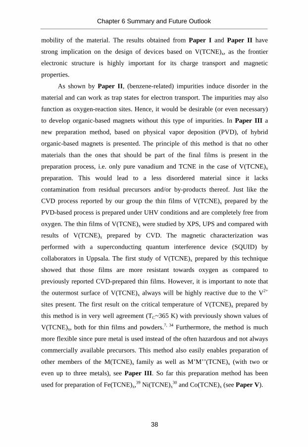
Figure 6.2 The spin valve structures based on V(TCNE)x. (a) With two identical FM
contacts. (b) With V(TCNE)x as soft magnet.48(c) With two different FM contacts.
The figure is adopted from Paper IV (copyright © Elsevier B.V.).
Since the goal is to fabricate spintronic devices based on V(TCNE)x, the
interface between FM metals and V(TCNE)x has strong implication of both the spin
injection and detection properties. In Paper IV the interfaces of Ni/V(TCNE)x as
well as of a model system, Ni/TCNE, were studied with PES and NEXAFS. The
results show that Ni interacts with both the cyano and the vinyl groups of TCNE in
V(TCNE)x. As chemical interaction affects both spin injection and detection
negatively by modifying the LUMO, likely destroying the magnetic network at the
surface, the results hence indicate that there is need for a buffer layer between Ni
and V(TCNE)x. Most likely this could be extended to be valid for V(TCNE)x and
any FM contact. In the same paper two new spin valve designs based on V(TCNE)x
were proposed. The basis of these new device designs is to use V(TCNE)x as spin-
transporting and spin-filtering layer sandwiched in between the two ferromagnetic
V(TCNE)x
Organic
FM
”ON” ”OFF”
V(TCNE)x
Organic
FM
”ON” ”OFF”
V(TCNE)x
FM1
FM2
FOUR POSSIBLE RESISTANCES:
V(TCNE)x
FM1
FM2
FOUR POSSIBLE RESISTANCES:
Chapter 6 Summary and Future Outlook
40
contacts, i.e. FM1/V(TCNE)x/FM2, instead of using V(TCNE)x as the soft magnetic
contact.48 These devices would make use of the fully spin-polarized transport levels
of V(TCNE)x and hence it would both enhance and preserve the spin polarizations
that are injected from the FM contacts. Two identical FM contacts could be used,
which is an advantage in the fabrication process point of view, or it could be built
with two different FM contacts. The former device would give the standard spin
valve on/off functionality, whereas the latter would enable four different resistances
to be obtained. To the best of our knowledge no device based on V(TCNE)x has
been realized so far, and remains a goal of our research.
As vanadium ions always are highly reactive towards e.g. oxygen, it would be
desirable to exchange vanadium in V(TCNE)x with another metal. The prerequisite
for such metal would be that it results in a magnet which is air stable,
semiconducting and magnetically ordered at room temperature. With the aim to
understand the key design criteria for developing organic-based magnets with
magnetic ordering above room temperature we have started to study M(TCNE)x
materials with significantly lower critical temperatures than room temperature and
compared them with V(TCNE)x. In Paper V we present the first results on the
electronic structure of Co(TCNE)x, (TC~44 K13) performed by XPS, NEXAFS and
resonant photoelectron spectroscopy (RPES). The XPS data suggests that
Co(TCNE)x contains local bonding disorder, unlike V(TCNE)x which can be grown
virtually defect free. The HOMO was determined by RPES to mainly be derived
from TCNE- units while the Co(3d) states are localized at higher binding energies.
This is in sharp contrast to the case for V(TCNE)x where V(3d) is mainly
responsible for the HOMO.36 However, it resembles the results of the electronic
structure that we have obtained previously for Fe(TCNE)x (TC~122 K13) for which
the HOMO also is TCNE--derived.39 Nevertheless, it was not possible to perform
calculations due to the lack of fine structure in the Co(TCNE)x Co L-edge NEXAFS
spectra. This could be done for both the Fe L-edge of Fe(TCNE)x39 and of the V L-
edge of V(TCNE)x,36 indicating that the crystal field in Co(TCNE)x is much weaker
than that of Fe(TCNE)x and especially weaker than the crystal field of V(TCNE)x.
However, the similarities in the electronic structure between Co(TCNE)x and
Fe(TCNE)x are in line with the significantly lower critical temperature as compared
Chapter 6 Summary and Future Outlook
41
to V(TCNE)x but if the reason for the lower critical temperature is due to the
disorder in the material, the very weak crystal field, or a combination of both is
however difficult to say.
6.3 Current Studies
Since V(TCNE)x reacts with FM metals (see Paper IV) this indicates the need
for a buffer layer between the two materials and we are currently focusing on
finding a proper material for this purpose. However, due to the very reactive nature
of V(TCNE)x this has shown to be an intricate task. For example LiF, which has
been frequently used as buffer layer in organic electronics,78 was deposited on top of
V(TCNE)x, but the results indicate that the fluorine reacts with the vanadium ions.
The most promising buffer layer so far seems to be alkyl chains (CH3(CH2)10CH3)
since the first results indicate no reaction between alkyl groups and vanadium or
TCNE. The use of long alkyl chains as buffer layers in organic electronics has
previously been demonstrated by other groups.79, 80
6.4 Future Outlook
It is difficult to predict the timescale before any product based on organic-
based magnets may reach the market. With properties such as low weight,
potentially cheaper production, biocompatibility, light-induced magnetism,
solubility in organic solvents etc.,2 they for sure have potential to be used in future
electronic products. One can draw parallels between the development of organic-
based magnets and organic electronics, conducting polymers were discovered in
1977,81 the first prototype device was demonstrated in 199082 and the first product
entered the market about 20 years after the first discovery (organic light emitting
diode (OLED) displays, by Tohoku Pioneer in 1999). Initially, conducting polymers
were thought of as replacement of metallic conductors.83 After a few years it was
realized that they are unable to compete with copper but they found a new
application area in LEDs. Today, mainly molecules, not polymers, are used. The
first room temperature organic-based magnet, V(TCNE)x, was discovered in 1991 as
a powder magnet and 10 years later the first thin films of the compound were
reported. Preparation as thin films was the first step towards applications and if
organic-based magnets follow the same timescale as organic electronics this would
Chapter 6 Summary and Future Outlook
42
mean that products could be on the market in approximately ten to twenty years
from now. However, due to the oxygen sensitivity of V(TCNE)x, its commercial
potential will depend on the effectiveness of sealing the device from atmospheric
contamination, nevertheless, it is an interesting material for pursuing research on
device physics, e.g. fabrication of spin valves. Similar to the case of organic
electronics, organic-based magnets are unlikely to compete with their metallic
counterparts. However, they have shown properties not seen in metallic magnets and
will most likely find their own application areas, e.g. in spintronics. It is worth to
note that they have also been suggested for other applications, such as functional
coatings on e.g. plastic or paper for microwave absorption and magnetic shielding.10
Before prototype devices based on organic-based magnets, in particular
V(TCNE)x, can be reality there are a number of issues that should be addressed.
First of all, it is important to find a suitable buffer layer to sandwich in between
V(TCNE)x and FM metals (as described in the paragraph above). Furthermore, it is
adequate, or even necessary, to increase the thin film growing speeds of the current
CVD- and PVD-based processes. This would save a lot of time when starting the
first attempts to fabricate devices based on V(TCNE)x.
Most likely, the first commercial applications will rely on a less air sensitive
magnets than V(TCNE)x. Therefore, the search for other room temperature
magnetically ordered semiconducting materials which are less air sensitive than
V(TCNE)x should also be continued.

�
43
References
1 M. Fahlman and W.R. Salaneck, Surfaces and interfaces in polymer-based
electronics, Surf. Sci. 500, 904 (2002). 2 J. Miller and A.J. Epstein, Molecule-Based Magnets- An Overview, MRS
Bullet. 25, 21 (2000). 3 J. Veciana and H. Iwamura, Organic Magnets, MRS Bullet. 25, 41 (2000). 4 A.J. Epstein, Organic-Based Magnets: Opportunities in Photoinduced
Magnetism, Spintronics, Fractal Magnetism and Beyond, MRS Bullet. 28,
492 (2003). 5 D.A. Pejakovic, C. Kitamura, J.S. Miller, and A.J. Epstein, Photoinduced
Magnetization in the Organic-Based Magnet Mn(TCNE)x·y(CH2Cl2), Phys.
Rev. Lett. 88, 057202 (2002). 6 J.S. Miller, Organic Magnets - A History, Adv. Mater. 14, 1105 (2002). 7 J.M. Manriquez, G.T. Yee, R.S. McLean, A.J. Epstein, and J.S. Miller, A
room-temperature molecular/organic-based magnet, Science 252, 1415
(1991). 8 P-M. Allemand, K.C. Khemani, A.F. Wudl, K. Holczer, S. Donovan, G.
Grüner, and J.D. Thompson, Organic molecular soft ferromagnetism in a
fullerene C60, Science 253, 301 (1991). 9 M. Takahashi, P. Turek, Y. Nakazawa, M. Tamura, K. Nozawa, D. Shiomi,
M. Ishikawa, and M. Kinoshita, Discovery of a quasi-1D organic
ferromagnet, p-NPNN, Phys. Rev. Lett. 67, 746 (1991). 10 A.J. Epstein and B.G. Morin, Molecular-based magnets comprising
vanadium tetracyanoethylene complexes for shielding electromagnetic fields,
US patent 5821453, 1998. 11 W.J.M. Naber, S. Faez, and W.G. van der Wiel, Organic spintronics, J. Phys.
D: Appl. Phys. 40, R205 (2007).
References
44
12 M.A. Gîr�u, C.M. Wynn, J. Zhang, J.S. Miller, and A.J. Epstein, Magnetic
properties and critical behavior of Fe(tetracyanoethylene)2·x(CH2Cl2): A
high-Tc molecule-based magnet, Phys. Rev. B 61, 492 (2000). 13 J. Zhang, J. Ensling, V. Ksenofontov, P. Gütlich, A.J. Epstein, and J.S.
Miller, [MII(tcne)2]·xCH2Cl2 (M = Mn, Fe, Co, Ni) Molecule-Based Magnets
with Tc Values above 100 K and Coercive Fields up to 6500 Oe, Angew.
Chem. Int. Ed. 37, 657 (1998). 14 C.M. Wynn, M.A. Gîr�u, J. Zhang, J.S. Miller, and A.J. Epstein, Reentrance
in the Mn(tetracyanoethylene)x·y(CH2Cl2) high-Tc molecule-based
ferrimagnet, Phys. Rev. B 58, 8508 (1998). 15 S. Blundell, Magnetism in Condensed Matter (Oxford University Press, New
York, 2001). 16 H. Benson, University Physics, (Wiley, New York, 1996). 17 C. Kittel, Introduction to Solid State Physics (John Wiley & Sons, 1996). 18 M.A. Gîr�u and M. Fahlman, Hybrid Organic-Inorganic Nanostructured
Magnets, in manuscript. 19 J-W. Yoo, R.S. Edelstein, D.M. Lincoln, N.P Raju, and A.J. Epstein,
Photoinduced Magnetism and Random Magnetic Anisotropy in Organic-
Based Magnetic Semiconductor V(TCNE)x Films, for x~2, Phys. Rev. Lett.
99, 157205 (2007). 20 E.B. Vickers, T.D. Selby, and J.S. Miller, Ni[TCNE]2·zCH2Cl2 (TC=13 K)
and VxNi1-x[TCNE]y·zCH2Cl2 solid solution room temperature magnets, J.
Am. Chem. Soc. 126, 3716 (2004). 21 D. de Caro, C. Faulmann, and L. Valade, Ligand Influence on Connectivity
and Processing: Magnetic Crystals Based on Metalloceniums and Films of
TCNE-Based Magnets (TCNE = Tetracyanoethylene) Chem. Eur. J. 13, 1650
(2007). 22 B.B. Kaul, M.A. Taylor, M.J. Whitton, and G.T. Yee, Beyond TCNE: new
building blocks for molecule-based magnets, Synth. Met. 122, 471 (2001). 23 E.B. Vickers, T.D. Selby, and J.S. Miller, Magnetically Ordered (TC=200 K)
Bis(tetracyanopyrazine)vanadium, V[TCNP]2·yCH2Cl2, J. Am. Chem. Soc.
126, 3716 (2003).
References
45
24 J.P. Fitzgerald, B.B. Kaul, and G.T. Yee,
Vanadium[dicyanoperfluorostilbene]2·yTHF: a molecule-based magnet with
TC�205 K, Chem. Commun. 1, 49 (1999). 25 K.I. Pokhodnya, V. Burtman, A.J. Epstein, J.W. Raebiger, and J.S. Miller,
Control of Coercivity in Organic-Based Solid Solution VxCo1-
x[TCNE]2·zCH2Cl2 Room Temperature Magnets, Adv. Mater. 15, 1211
(2003). 26 E.B. Vickers, A. Senesi, and J.S. Miller, Ni[TCNE]2·zCH2Cl2 (Tc =13 K) and
VxNi1-x[TCNE]y·zCH2Cl2 solid solution room temperature magnets, Inorg.
Chim. Acta 357, 3889 (2004). 27 K.I. Pokhodnya, E.B. Vickers, M. Bonner, A.J. Epstein, and J.S. Miller,
Solid solution VxFe1-x[TCNE]2·zCH2Cl2 room-temperature magnets, Chem.
Mater. 16, 3218 (2004). 28 R. Jain, K. Kabir, J.B. Gilroy, K.A.R. Mitchell, K-C. Wong, and R.G. Hicks,
High-temperature metal-organic magnets, Nature 445, 291 (2007). 29 J.S. Miller and K.I. Pokhodnya, Formation of Ni[C4(CN)8]from the reaction
of Ni(COD)2(COD=1,5-cyclooctadiene) with TCNE in THF, J. Mater. Chem.
17, 3585 (2007). 30 P. Bhatt, A. Kanciurzewska, E. Carlegrim, M. Kapilashrami, L. Belova, K.V.
Rao, and M. Fahlman, Ferromagnetism above room temperature in nickel-
tetracyanoethylene thin films, J. Mater. Chem. 19, 6610 (2009). 31 D. Haskel, Z. Islam, J. Lang, C. Kmety, G. Srajer, K.I. Pokhodnya, A.J.
Epstein, and J.S. Miller, Local structural order in the disordered vanadium
tetracyanoethylene room-temperature molecule-based magnet, Phys. Rev. B.
70, 054422 (2004). 32 N.P. Raju, V.N. Prigodin, K.I. Pokhodnya, J.S. Miller, and A.J. Epstein, High
field linear magnetoresistance in fully spin-polarized high-temperature
organic-based ferrimagnetic semiconductor V(TCNE)x films, x~2, Synth.
Met. 160, 307 (2010). 33 V.N. Prigodin, N.P. Raju, K.I. Pokhodnya, J.S. Miller, and A.J. Epstein,
Electronic Spin-Driven Resistance in Organic-Based Magnetic
Semiconductor V[TCNE]x, Synth. Met. 135, 87 (2003).
References
46
34 K.I. Pokhodnya, D. Pejakovic, A.J. Epstein, and J.S. Miller, Effect of solvent
on the magnetic properties of the high-temperature V[TCNE]x molecule-
based magnet, Phys. Rev. B 63, 174408 (2001). 35 J.B. Kortright, D.M. Lincoln, R.S. Edelstein, and A.J. Epstein, Bonding,
Backbonding and Spin-Polarized Molecular Orbitals: Basis for Magnetism
and Semiconducting Transport in V[TCNE]x~2, Phys. Rev. Lett. 100, 257204
(2008). 36 C. Tengstedt, M.P. de Jong, A. Kanciurzewska, E. Carlegrim, and M.
Fahlman, X-Ray Magnetic Circular Dichroism and Resonant Photoemission
of V(TCNE)x Hybrid Magnets, Phys. Rev. Lett. 96, 057209 (2006). 37 M.P. de Jong, C. Tengstedt, A. Kanciurzewska, E. Carlegrim, W.R.
Salaneck, and M. Fahlman, Chemical bonding in V(TCNE)x (x~2) thin-film
magnets grown in situ, Phys. Rev. B 75, 064407 (2007). 38 C. Tengstedt, M. Unge, M.P. de Jong, S. Stafström, W.R. Salaneck, and M.
Fahlman, Coulomb interaction in rubidium-doped tetracyanoethylene: a
model system for organometallic magnets, Phys. Rev. B 69, 165208 (2004). 39 P. Bhatt, E. Carlegrim, A. Kanciurzewska, M.P. de Jong, and M. Fahlman,
Electronic structure of thin film iron-tetracyanoethylene: Fe(TCNE)x, Appl.
Phys. A 95, 131 (2009). 40 S.A. Wolf and D. Treger, Spintronics: A new paradigm for electronics for the
new millennium, IEEE Trans. Magn. 36, 2748 (2000). 41 S.A. Wolf, D.D. Awschalom, R.A. Buhrman, J.M. Daughton, S.V. Molnár,
M.L. Roukes, A.Y. Chtelkanova, and D.M. Treger, Spintronics: A spin-based
electronics vision for the future, Science 294, 1488 (2001). 42 A. Wallerius, Elektronernas spinn styr framtidens elektronik, Ny Teknik nr 6,
14 (2003). 43 S.A. Wolf, D. Treger, and A. Chtchelkanova, Spintronics: The future of data
storage?, MRS Bullet. 31, 400 (2006). 44 http://nobelprize.org/nobel_prizes/physics/laureates/2007/phyadv07.pdf
Accessed April 15, 2010. 45 J. Camarero and E. Coronado, Molecular vs. inorganic spintronics: the role of
molecular materials and single molecules, J. Mater. Chem. 19, 1678 (2009).
References
47
46 F. Wang and Z.V. Vardeny, Organic spin valves: the first organic spintronics
devices, J. Mater. Chem. 19, 1685 (2009). 47 G.A. Prinz, Magnetoelectronics, Science 282, 1660 (1998). 48 A.J. Epstein and V.N. Prigodin, Polymer-, organic-, and molecular-based
spintronic devices, US patent application 20030001154, 2003. 49 J.S. Miller and A.J. Epstein, Organic and Organometallic Molecular
Magnetic Materials - Designer Magnets, Angew. Chem. Int. Ed. Engl. 33, 385
(1994). 50 M.S. Thorum, K.I. Pokhodnya, and J.S. Miller, Solvent enhancement of the
magnetic ordering temperature (Tc) of the room temperature V(TCNE)x·S (S
= solvent, TCNE=tetracyanoethylene; x~2) magnet, Polyhedron 25, 1927
(2006). 51 J.S. Miller, Organometallic- and organic-based magnets: new chemistry and
new materials for the new millennium, Inorg. Chem. 39, 4392 (2000). 52 M. Ohring, Materials Science of Thin Films (Academic Press, Boston, 2002). 53 P. van Zant, Microchip fabrication: a practical guide to semiconductor
processing (McGraw-Hill, New York, 2000). 54 D. de Caro, M. Basso-Bert, J. Sakah, H. Casellas, J-P. Legros, L. Valade, and
P. Cassoux, CVD-grown Thin Films of Molecule-Based Magnets, Chem.
Mater. 12, 587 (2000). 55 K.I. Pokhodnya, A.J. Epstein, and J.S. Miller, Thin-film V[TCNE]x magnets,
Adv. Mater. 12, 410 (2000). 56 G.E. Muilenberg ed., Handbook of X-ray photoelectron spectroscopy
(Perkin-Elmer Corporation, Minnesota, 1979). 57 L. Nemec, L. Chia, and P. Delahay, Photoelectron spectroscopy of liquids:
external ionization energies, J. Electron Spectrosc. Relat. Phenom. 9, 241
(1976). 58 S. Hagström, C. Nordling, and K. Siegbahn, Electron Spectroscopy for
Chemical Analysis, Phys. Lett. 9, 235 (1964). 59 S. Hüfner, Photoelectron spectroscopy: Principle and applications (Springer
Verlag, Berlin, 2003).
References
48
60 C. Nordling, E. Sokolowski, and K. Siegbahn, Precision method for
obtaining absolute values of atomic binding energies, Phys. Rev. 105, 1676
(1957). 61 W.R. Salaneck, S. Stafström, and J-L. Brédas, Conjugated polymer surfaces
and interfaces (Cambridge University Press, Cambridge, 1996). 62 A. Zangwill, Physics at surfaces (Cambridge University Press, Cambridge,
1988). 63 D. Briggs and M.P. Seah eds., Practical Surface Analysis (John Wiley and
Sons, West Sussex, 1990). 64 N. Mårtensson and A. Nilsson, On the origin of core-level binding energy
shifts J. Electron Spectrosc. Relat. Phenom. 75, 209 (1995). 65 G. Wendin, Breakdown of the one-electron picture in photoelectron spectra
(Springer-Verlag, New York, 1981). 66 D.W. Turner and M.L.A. Jobory, Determination of ionization potentials by
photoelectron energy measurements, J. Chem. Phys. 37, 3007 (1962). 67 C. Tengstedt, Materials study of organic electronics, Linköping University,
2005. 68 D. Attwood, Soft X-rays and extreme ultraviolet radiation (Cambridge
university press, Cambridge, 1999). 69 H. Winick and S. Doniach eds., Synchrotron Radiation Research (Plenum
Press, New York, 1980). 70 http://www.maxlab.lu.se Accessed April 15, 2010. 71 J. Stöhr, NEXAFS spectroscopy (Springer-Verlag, Berlin, 1996). 72 P.A. Brühwiler, O. Karis, and N. Mårtensson, Charge-transfer dynamics
studied using resonant core spectroscopies, Rev. Mod. Phys. 74, 703 (2002). 73 L.A. Engström, Elektromagnetism Från bärnsten till fältteori
(Studentlitteratur, Lund, 2000). 74 I. Soroka, Magnetic heterostructures: the effect of compositional modulation
of magnetic properties, Uppsala University, 2005. 75 S. Felton, Tunable magnetic properties of transition metal compounds,
Uppsala University, 2005.
References
49
76 R. Nyholm, J.N. Andersen, U. Johansson, B.N. Jensen, and I. Lindau,
Beamline I311 at MAX-lab: a VUV/soft X-ray undulator beamline for high
resolution electron spectroscopy, Nucl. Instr. and Meth. in Phys. Res. A 467,
520 (2001). 77 http://www.maxlab.lu.se/beamline/max-ii/d1011/d1011.html Accessed April
15, 2010. 78 S.K.M. Jönsson, E. Carlegrim, F. Zhang, W.R. Salaneck, and M. Fahlman,
Photoelectron spectroscopy of the contact between the cathode and the active
layers in plastic solar cells, Jpn J. Appl. Phys. 44, 3695 (2005). 79 N. Ueno, H. Fujimoto, N. Sato, K. Seki, and H. Inokuchi, Angle-Resolved
Photoemission from Oriented Thin Films of Long Alkyl Molecules: Valence
Band Dispersion, Phys. Scr. 41, 181 (1990). 80 K. Seki, N. Ueno, U.O. Karlsson, and R. Engelhardt, Valence bands of
oriented finite linear chain molecular solids as model compounds of
polyethylene studied by angle-resolved photoemission, Chem. Phys. 105, 247
(1986). 81 C.K. Chiang, C.R. Fincher, Y.W. Park, A.J. Heeger, H. Shirakawa, E.J.
Louis, S.C. Gau, and A.G. MacDiarmid, Electrical Conductivity in Doped
Polyacetylene, Phys. Rev. Lett. 39, 1098 (1977). 82 J.H. Burroughes, D.D.C. Bradley, A.R. Brown, R.N. Marks, K. Makay, R.H.
Friend, P.L. Burn, and A.B. Holmes, Light emitting diodes based upon
conjugated polymers, Nature 347, 539 (1990). 83 A.J. Heeger, Semiconducting and Metallic Polymers: The Fourth Generation
of Polymeric Materials (Nobel Lecture), Angew. Chem. Int. Ed. 40, 2591
(2001).

![Giant Hysteresis of Single‐Molecule Magnets Adsorbed on a ...Single-molecule magnets (SMMs) [ 1 ] are very promising for molecular spintronics [ 2 ] and quantum information processing,](https://img.pdfslide.us/doc/110x75/5f7183ee583523514d683f7a/giant-hysteresis-of-singleamolecule-magnets-adsorbed-on-a-single-molecule.jpg)


![Spintronics [EDocFind.com]](https://img.pdfslide.us/doc/110x75/577d2e0b1a28ab4e1eaea99b/spintronics-edocfindcom.jpg)