Embed Size (px)
Citation preview

DEVELOPMENT OF MULTILAYER LIQUID CRYSTAL POLYMER
BASED RADIO FREQUENCY FRONT-END
RECEIVING MODULE AT W-BAND
by
Yifei Zhang
A dissertation submitted to the Faculty of the University of Delaware in partial fulfillment of the requirements for the degree of Doctor of Philosophy in Electrical and Computer Engineering
Spring 2016
© 2016 Yifei Zhang All Rights Reserved

All rights reserved
INFORMATION TO ALL USERSThe qua lity o f this rep roduction is dependent upon the qua lity o f the copy submitted .
In the unlike ly event tha t the author d id no t send a comp le te manuscrip tand the re a re missing pages, these will be no ted . Also , if ma te ria l had to be removed ,
a no te will ind ica te the de le tion.
All rights reserved .
This work is p ro tected aga inst unauthorized copying under Title 17, United Sta tes CodeMicro fo rm Ed ition © ProQuest LLC.
ProQuest LLC.789 East Eisenhower Parkway
P.O. Box 1346Ann Arbor, MI 48106 - 1346
ProQuest 10156508
Pub lished by ProQuest LLC (2016). Copyright o f the Disserta tion is he ld by the Author.
ProQuest Number: 10156508

DEVELOPMENT OF MULTILAYER LIQUID CRYSTAL POLYMER
BASED RADIO FREQUENCY FRONT-END
RECEIVING MODULE AT W-BAND
by
Yifei Zhang
Approved: __________________________________________________________ Kenneth E. Barner, Ph.D. Chair of the Department of Electrical and Computer Engineering Approved: __________________________________________________________ Babatunde Ogunnaike, Ph.D. Dean of the College of Engineering Approved: __________________________________________________________ Ann L. Ardis, Ph.D. Senior Vice Provost for Graduate and Professional Education

I certify that I have read this dissertation and that in my opinion it meets the academic and professional standard required by the University as a dissertation for the degree of Doctor of Philosophy.
Signed: __________________________________________________________ Dennis W. Prather, Ph.D. Professor in charge of dissertation
I certify that I have read this dissertation and that in my opinion it meets the academic and professional standard required by the University as a dissertation for the degree of Doctor of Philosophy.
Signed: __________________________________________________________ Mark S. Mirotznik, Ph.D. Member of dissertation committee
I certify that I have read this dissertation and that in my opinion it meets the academic and professional standard required by the University as a dissertation for the degree of Doctor of Philosophy.
Signed: __________________________________________________________ Keith W. Goossen, Ph.D. Member of dissertation committee
I certify that I have read this dissertation and that in my opinion it meets the academic and professional standard required by the University as a dissertation for the degree of Doctor of Philosophy.
Signed: __________________________________________________________ Shouyuan Shi, Ph.D. Member of dissertation committee
I certify that I have read this dissertation and that in my opinion it meets the academic and professional standard required by the University as a dissertation for the degree of Doctor of Philosophy.
Signed: __________________________________________________________ Richard D. Martin, Ph.D. Member of dissertation committee

iv
There are many people to whom I must express my deepest gratitude. Without
their helps and encouragements, this dissertation would never have been completed.
First, I must thank my advisor, Dr. Dennis W. Prather, whose guidance,
persistence, and vision have been the guiding light for my research. Your belief and
support have encouraged me throughout the whole journey. You have been a great
mentor and inspired me to broaden my horizon.
To all the members of this community, I must express my sincerest thanks. I
would like to particularly thank: Dr. Shouyuan Shi for your brilliant guidance,
valuable suggestions, and kind patience throughout this process, Dr. Richard D.
Martin for your remarkable management and coordination in this research and
irreplaceable experiences and contributions in device manufacturing and measurement,
Dr. Peng Yao for your outstanding integration techniques and professional suggestions
in the millimeter wave measurement, Andrew A. Wright and Kevin Shreve for your
excellent integration and packaging techniques. I would also like to thank my
colleagues, Dr. Christopher A. Schuetz, Dr. Garrett Schneider, Dr. Janusz Murakowski,
Dr. Rownak Shireen, Dr. Yuehao Wu, Dr. Jian Bai, Dr. David Eng, Dr. David W.
Grund, Stephen Kozacik, Maciej Murakowski, Matthew R. Konkol, Andrew Mercante,
Dylan Ross, and the rest of the group members for your great helps and sharing your
experience in this work. May our friendships last a lifetime.
I would like to express my most genuine thanks to: all the members of my
committee for reviewing my dissertation, attending my defense, and helping me
ACKNOWLEDGMENTS

v
through this process, Mr. Bruce Wallace and other program officers at Defense
Advanced Research Projects Agency (DARPA) for generously supporting this work,
Jesse Ward and Brent Mayfield at Compunetics Inc. for your great supports in
fabrication and manufacturing.
Finally, I would like to thank my family and friends. To my father, thank you
for teaching me the persistence and providing me the foundation to allow me to make
this journey. To my mother, thank you for your unconditional love, support, and
encouragement throughout my life. To my aunt, thank you for exciting me the self-
confidence and faith to reach the final destination. To Dr. Tian Gu and Dr. Liang Qiu,
thank you for your selfless helps and precious friendships in the department.

vi
LIST OF TABLES ......................................................................................................... xLIST OF FIGURES ....................................................................................................... xiABBREVATIONS ....................................................................................................... xvABSTRACT .............................................................................................................. xviii Chapter
1 INTRODUCTION .............................................................................................. 1
1.1 Millimeter Wave Frequencies ................................................................... 11.2 W-band Frequencies and Their Challenges ............................................... 3
1.2.1 PCB Materials ............................................................................... 41.2.2 Fabrication Limits ......................................................................... 71.2.3 Electromagnetic Interference ......................................................... 81.2.4 Measurement Limits ...................................................................... 9
1.3 Wireless Systems and Their Applications at W-band ............................. 10
1.3.1 Wireless Communication Systems .............................................. 101.3.2 Radar Systems ............................................................................. 121.3.3 Radiometry Systems .................................................................... 14
1.4 W-band Front-End Receiving Module in Multilayer LCP Substrates .... 17
1.4.1 State-of-The-Art .......................................................................... 171.4.2 Multilayer Circuitry ..................................................................... 18
1.5 Dissertation Outline ................................................................................. 191.6 List of Original Contributions ................................................................. 20
2 HIGH-GAIN LINEARLY TAPERED ANTIPODAL SLOT ANTENNA AT E- AND W-BANDS ................................................................................... 26
2.1 System Aspects of Receiving Antennas .................................................. 262.2 Challenges for W-band Antennas ............................................................ 28
TABLE OF CONTENTS

vii
2.2.1 Design Aspect .............................................................................. 282.2.2 Measurement Aspect ................................................................... 29
2.3 Linearly Tapered Antipodal Slot Antenna .............................................. 30
2.3.1 LTASA Design ............................................................................ 322.3.2 Bandwidth Measurement ............................................................. 372.3.3 Far-field Measurement ................................................................ 38
2.3.3.1 Optically addressed far-field measurement system ...... 382.3.3.2 Characterized radiation patterns and gain .................... 41
2.4 Summary .................................................................................................. 42
3 TRANSITIONS IN MULTILAYER LCP SUBSTRATES ............................. 44
3.1 Transmission Lines and Waveguides ...................................................... 443.2 CBCPW-to-Stripline Vertical Transition ................................................ 47
3.2.1 Transition Design ........................................................................ 483.2.2 Measurement ............................................................................... 50
3.2.2.1 System set-up ................................................................ 503.2.2.2 Back-to-back transition ................................................ 52
3.3 MS-to-SIW Transition ............................................................................. 54
3.3.1 Transition Design ........................................................................ 553.3.2 Measurement ............................................................................... 57
3.3.2.1 CBCPW probe pad ....................................................... 573.3.2.2 Back-to-back transition ................................................ 59
3.4 SIW-to-Waveguide Transition ................................................................ 61
3.4.1 Transition Design ........................................................................ 623.4.2 Measurement ............................................................................... 65
3.5 MS-to-CPW Transition ........................................................................... 67
3.5.1 Transition Design ........................................................................ 683.5.2 Measurement ............................................................................... 69
3.6 Summary .................................................................................................. 71

viii
4 MULTI-CHIP MODULE INTEGRATION AND PACKAGE ....................... 72
4.1 NG ALP283 Low Noise Amplifier ......................................................... 744.2 Multilayer-LCP MMIC Carrier ............................................................... 764.3 V-Shape Wire Bond ................................................................................ 784.4 Multi-Chip Module .................................................................................. 82
4.4.1 Single-LNA Module .................................................................... 824.4.2 Double-LNA Module .................................................................. 83
4.5 Packaging Technologies .......................................................................... 874.6 Summary .................................................................................................. 87
5 SIW FILTER AND DIRECTIONAL FILTER AT W-BAND ........................ 89
5.1 Challenges for W-band Filters ................................................................. 905.2 SIW Filter at 94 GHZ .............................................................................. 92
5.2.1 SIW Filter Design ........................................................................ 935.2.2 Measurement ............................................................................... 96
5.3 Directional Filters at 95 GHZ .................................................................. 96
5.3.1 Directional Coupler Design ......................................................... 99
5.3.1.1 Slot coupling of the vertically overlapped MS lines .. 1005.3.1.2 Dual-slot directional coupler ...................................... 102
5.3.2 Directional Filter Design ........................................................... 104
5.3.2.1 Single-loop directional filter ....................................... 106
5.3.2.1.1 Symmetric loop ........................................ 1065.3.2.1.2 Asymmetric loop ...................................... 107
5.3.2.2 Double-loop directional filter ..................................... 108
5.3.3 Hybrid Substrates and Measurement ......................................... 111
5.3.3.1 Hybrid substrates ........................................................ 1115.3.3.2 Measurement set-up and W-band load ....................... 1125.3.3.3 Measured S-parameters .............................................. 113
5.3.3.3.1 Single-loop DFs ........................................ 1145.3.3.3.2 Cascaded double-loop DFs ....................... 114

ix
5.4 Summary ................................................................................................ 117
6 CONCLUSION AND FUTURE WORK ....................................................... 119
6.1 Conclusion ............................................................................................. 1196.2 Future Work ........................................................................................... 122
REFERENCES ........................................................................................................... 126 Appendix
COPYRIGHT PERMISSION ........................................................................ 136

x
Table 1.1. Material properties of traditional and new PCB substrates [4] and [6]-[8]. .............................................................................................................. 6
Table 2.1. Optimized dimensions of the proposed LTASA. ..................................... 34
Table 2.2. Simulated gain, beamwidth, first sidelobe, and cross-polarization of the proposed LTASA. .............................................................................. 35
Table 3.1. Fundamental mode, dimensions, and simulated propagation loss and impedance at W-band of the five planar transmission components on a 100μm thick LCP substrate and WR-10 rectangular waveguide. ............ 46
Table 3.2. Cut-off frequency of the SIWs and dimensions of the corresponding MS-to-SIW transitions. ............................................................................ 56
Table 4.1. Resistance, inductance, and capacitance of the circuit module for the V-shape wire bond. .................................................................................. 81
Table 5.1. Material properties of the substrates and dimensions of the HFSS models and fabricated devices ............................................................... 113
Table 5.2. Insertion loss, bandwidth, and out-of-band rejection of the directional filters. ..................................................................................................... 116
LIST OF TABLES
xi
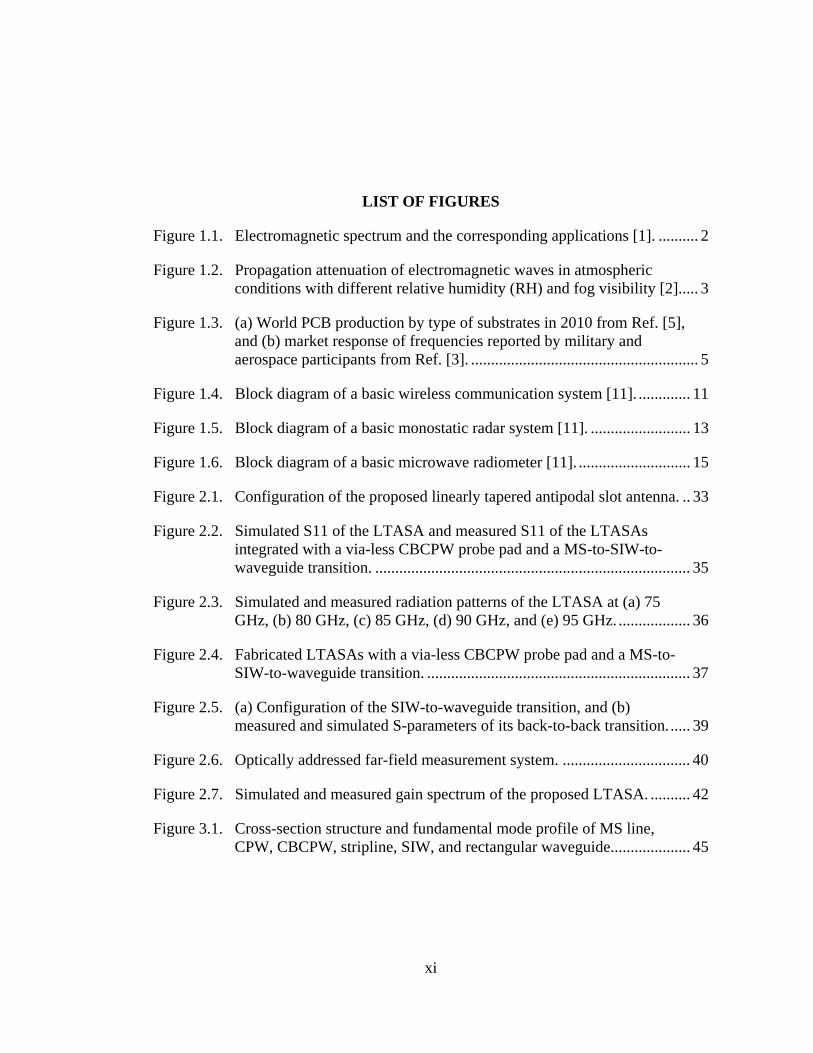
Figure 1.1. Electromagnetic spectrum and the corresponding applications [1]. .......... 2
Figure 1.2. Propagation attenuation of electromagnetic waves in atmospheric conditions with different relative humidity (RH) and fog visibility [2]. .... 3
Figure 1.3. (a) World PCB production by type of substrates in 2010 from Ref. [5], and (b) market response of frequencies reported by military and aerospace participants from Ref. [3]. ......................................................... 5
Figure 1.4. Block diagram of a basic wireless communication system [11]. ............. 11
Figure 1.5. Block diagram of a basic monostatic radar system [11]. ......................... 13
Figure 1.6. Block diagram of a basic microwave radiometer [11]. ............................ 15
Figure 2.1. Configuration of the proposed linearly tapered antipodal slot antenna. .. 33
Figure 2.2. Simulated S11 of the LTASA and measured S11 of the LTASAs integrated with a via-less CBCPW probe pad and a MS-to-SIW-to-waveguide transition. ............................................................................... 35
Figure 2.3. Simulated and measured radiation patterns of the LTASA at (a) 75 GHz, (b) 80 GHz, (c) 85 GHz, (d) 90 GHz, and (e) 95 GHz. .................. 36
Figure 2.4. Fabricated LTASAs with a via-less CBCPW probe pad and a MS-to-SIW-to-waveguide transition. .................................................................. 37
Figure 2.5. (a) Configuration of the SIW-to-waveguide transition, and (b) measured and simulated S-parameters of its back-to-back transition. ..... 39
Figure 2.6. Optically addressed far-field measurement system. ................................ 40
Figure 2.7. Simulated and measured gain spectrum of the proposed LTASA. .......... 42
Figure 3.1. Cross-section structure and fundamental mode profile of MS line, CPW, CBCPW, stripline, SIW, and rectangular waveguide.................... 45
LIST OF FIGURES
xii
Figure 3.2. (a) Cross section and (b) layer-by-layer configuration and dimensions of the CBCPW-to-SL transition. .............................................................. 49
Figure 3.3. Simulated S-parameters of a CBCPW-to-SL transition: (a) tolerance analysis of the diameter of the blind via, and (b) tolerance analysis of the pitch between the blind and through vias. .......................................... 51
Figure 3.4. (a) Fabricated CBCPW-to-SL-to-CBCPW transition, and (b) cross-section cut of the fabricated back-to-back transition. .............................. 52
Figure 3.5. Simulated and measured S-parameters of the back-to-back transition with a 3 mm long SL. ............................................................................... 53
Figure 3.6. Configuration of the MS-to-SIW transition. ............................................ 56
Figure 3.7. Simulated S-parameters of a MS-to-SIW transition (� = 1.7 mm). ........ 57
Figure 3.8. (a) Configuration of a CBCPW probe pad and its back-to-back transition,(b) simulated and measured S-parameters of a 5mm long MS line terminated with a pair of probe pads, and (c) calculated propagation loss of a MS line and insertion loss of a pair of probe pads. ......................................................................................................... 58
Figure 3.9. (a) Fabricated MS-to-SIW-to-MS transition, and (b) simulated and measured S-parameters of the back-to-back transition (� = 1.7 mm). .... 60
Figure 3.10. Configuration and dimensions of the SIW-to-WG transition in multilayer LCP substrates. ....................................................................... 63
Figure 3.11. (a) Propagation and cross-section of the fundamental and parasitic modes of the proposed SIW-to-WG transition, and simulated (b) S11 and (c) S21 of the transition with varying L at W-band. ......................... 64
Figure 3.12. (a) Fabricated waveguide-to-SIW-to-waveguide transition with metal housing, and (b) simulated and measured S-parameters of the back-to-back transition. ......................................................................................... 66
Figure 3.13. Configuration of the MS-to-CPW transition. ........................................... 69
Figure 3.14. (a) Fabricated MS-to-CPW transition with a CBCPW probe pad, and (b) simulated and measured S-parameters of this transition. ................... 70
Figure 4.1. (a) Top view, (b) measured on-chip gain, and (c) calculated input and output impedances of the NG ALP283 LNA. .......................................... 75

xiii
Figure 4.2. Layer-to-layer circuit schematic of the multilayer LCP carrier. .............. 77
Figure 4.3. (a) Configuration of the V-shape wire bond and traditional single wire bond, (b) simulated S-parameters of these two wire bonds as well as the circuit module (CM) of the V-shape wire bond, and (c) calculated input and output impedances of the wire bonds. ...................................... 79
Figure 4.4. Equivalent circuit model of the proposed V-shape wire bond. ................ 81
Figure 4.5. (a) Configuration of the single-LNA module, (b) simulated net loss of the single-LNA module and double-LNA module, and (c) measured and calculated net gain of the single-LNA module. ................................. 83
Figure 4.6. Packaged double-LNA module and 3-D printed housing. ....................... 84
Figure 4.7. Measured and calculated (a) net gain, (b) unwrapped phase, and (c) noise figure of the double-LNA module. ................................................. 86
Figure 5.1. Configuration of the second-ordered SIW filter fed by MS lines. ........... 94
Figure 5.2. (a) Fabricated second-ordered SIW filter, and (b) simulated and measured S-parameters of the SIW filter. ................................................ 95
Figure 5.3. Traditional directional filters: (a) waveguide-based, (b) standing-wave I, (c) standing-wave II, and (d) travelling-wave. ..................................... 97
Figure 5.4. (a) Configuration, electric fields, and equivalent circuit models of the slot-coupled vertically overlapped MS lines, and simulated S-parameters of the slot-coupled MS lines with (b) different LCP thickness and (c) slot size. ...................................................................... 101
Figure 5.5. (a) Configuration, (b) simulated S11 and S31, and (c) simulated S21 and S41 of the directional coupler in LCP substrates and hybrid substrates. ............................................................................................... 103
Figure 5.6. (a) Configuration of the single-loop DFs with symmetric and asymmetric loop topologies in multilayer LCP substrates, and simulated S-parameters of the (b) symmetric and (c) asymmetric DFs with ps = 0.35 mm. ................................................................................. 105
Figure 5.7. Simulated (a) effective dielectric constant and (b) loss of MS lines with a width of 160 μm on a 100μm LCP substrate and a 50μm LCP substrate laminated with a 66μm AG bond-ply. .................................... 106

xiv
Figure 5.8. (a) Configuration of the cascaded double-loop DF with asymmetric loops, and simulated S-parameters of the cascaded DF with Pd = (b) 1.9 mm and (c) 2.3 mm. ......................................................................... 109
Figure 5.9. Fabricated single-loop and cascaded DFs with RF absorbers. ............... 113
Figure 5.10. Measured and simulated S-parameters of (a) the asymmetric single-loop DF with ps = 0.37 mm and cascaded double-loop DFs with Pd = (b) 1.9mm and (c) 2.3 mm. .................................................................... 115
Figure 6.1. Configuration of a multilayer LCP-based ultra-wideband front-end module. ................................................................................................... 122
Figure 6.2. Passive mmW imager at 77 GHz. .......................................................... 124
Figure 6.3. Packaged receiving module based on multilayer LCP substrates for mmW imaging at 95 GHz. ..................................................................... 125

xv
RF: Radio Frequency
IR: Infrared
mmW: Millimeter Wave
AM: Amplitude Modulation
FM: Frequency Modulation
TV: Television
GPS: Global Positioning System
RFID: Radio Frequency Identification
HDI: High Density Interconnection
PCB: Printed Circuit Board
CTE: Coefficient of Thermal Expansion
PTFE: Polytetrafluoroethylen
LTCC: Low Temperature Co-fired Ceramic
LCP: Liquid Crystal Polymer
EMI: Electromagnetic Interference
RFI: Radio-Frequency Interference
EMC: Electromagnetic Compatibility
DUT: Device Under Test
SMC: Surface-Mounted Connector
G-S-G: Ground-Single-Ground
WLAN: Wireless Local Area Network
ABBREVATIONS

xvi
DBS: Direct Broadcast Satellite
FCC: Federal Communication Commission
RCS: Radar Cross Section
ECCM: Electronic Counter-countermeasures
LNA: Low Noise Amplifier
IF: Intermedium Frequency
SNR: Signal-to-Noise Ratio
SWaP: Size, Weight, and Power
LTASA: Linearly Tapered Antipodal Slot Antenna
CBCPW: Conductor-Backed Co-Planar Waveguide
MS: Microstrip
SIW: Substrate Integrated Waveguide
UWB: Ultra-Wideband
NF: Noise Figure
AUT: Antenna Under Test
TSA: Tapered Slot Antenna
CPW: Co-Planar Waveguide
PA: Power Amplifier
ASL: Antipodal Slot-line
APSL: Antipodal Parallel Stripline
HFSS: High Frequency Structural Simulator
SOLT: Short-Open-Load-Through
PNA: Programmable Network Analyzer
EO: Electro-Optic

xvii
DWDM: Dense Wavelength Division Multiplexing
SL: Stripline
FEM: Finite Element Method
RWG: Rectangular Waveguide
MMIC: Monolithic Microwave/Millimeter Integrated Circuit
MCM: Multi-Chip Module
SOP: System On Package
SCM: Single-Chip Module
ADS: Advanced Design System

xviii
To extend the sensing of human vision, radio frequencies have found prolific
wireless applications in everyday life, e.g., wireless communication, radar, and
radiometry. To overcome the crowded microwave spectrum, millimeter wave (mmW)
frequencies have gained tremendous interest in these systems within several spectral
windows, i.e., 35 GHz, 77 GHz, 95 GHz, and 140 GHz, due to their low atmospheric
propagation loss. Additionally, mmWs can provide gigabyte data transmission rates
for wireless communication systems and high resolution for radar and radiometry
systems. To date, most mmW wireless systems have been implemented at Ka-band,
i.e., 35 GHz, where they can be directly extended from the traditional microwave
systems. However, as the frequency increases to W-band, such as 77 GHz and 95 GHz,
RF engineers encounter nontrivial challenges from various technical aspects.
In a general sense, the most critical part of wireless communication, radar, and
radiometry systems is the receiver. Despite the different mechanisms and applications
of these receivers, it should be noted that they have similar front-end components, i.e.,
antennas, pre-amplifiers, and filters. Assembling these components can achieve a
front-end receiving module, which could potentially be utilized in most wireless
systems.
To this end, I present my work on the development of a W-band front-end
receiving module, consisting of a high-gain antenna, high-gain low noise amplifiers,
bandpass filters, transmission lines, and their transitions for interconnection. To
ABSTRACT

xix
minimize the dielectric loss, liquid crystal polymer (LCP) is selected as the module
substrate, which has a low loss tangent and low dielectric constant at W-band. To
achieve high density, light weight, low profile, and low power consumption, the
proposed module is designed on a multilayer circuit. The multilayer circuit is
fabricated using the commercial state-of-the-art large-panel circuit print technologies,
achieving low unit price and short manufacturing cycle. Multi-chip module packaging
technologies have been developed to achieve a net gain of more than 50 dB for the
proposed module, while maintaining linear phase and low electromagnetic
interference. By using the state-of-the-art low noise amplifiers, the noise figure of the
module can be minimized below 6 dB at W-band, which can satisfy most wireless
receiving applications. The designed antenna, transitions between various transmission
lines, low noise amplifies, and developed integration and packaging technologies
achieve an ultra-wide bandwidth that covers most of the frequencies in the W-band,
providing sufficient bandwidth for gigabyte data transmission rates in wireless
communication systems. For narrow-band applications, i.e., radiometry and frequency
division multiplexing, the designed filters and directional filters can be utilized to pick
out the frequencies of interest. In conclusion, the proposed front-end receiving module
may find many applications in various wireless systems at W-band, i.e., wireless
communication, radar, and radiometry.

1
INTRODUCTION
1.1 Millimeter Wave Frequencies
Visible light, mainly emitted by our sun, is located within an electromagnetic
spectrum with a wavelength between 390 and 700 nm. To sense objects in other
regions of the electromagnetic spectrum, such as radio frequency (RF), infrared (IR),
and X-ray, various instrumental technologies have been developed. For instance, RF
radar systems provide significantly larger range and resistance to atmospheric
disturbances for remote sensing and tracking. IR cameras provide night vision by
capturing terrestrial temperature radiation at wavelengths of approximately ten
microns. X-ray systems have been utilized for medical and security screening due to
their ability to penetrate optically opaque materials. To date, electromagnetic
frequencies have found prolific irreplaceable applications in our daily life, such as
amplitude modulation (AM)/frequency modulation (FM) radio, television (TV)
broadcast, global positioning system (GPS), remote control, wireless communication,
fiber optic communication, astronomy, and RF identification (RFID).
However, it should be noted that there exists a region of the electromagnetic
spectrum, between microwave and IR frequencies, with relatively less exploration,
which is referred to as the millimeter wave (mmW) region. As its name implies, mmW
spectrum has a wavelength measured on the order of millimeters in free space and
extends from 30 to 300 GHz, as can be seen in Figure 1.1. Typically, the microwave
spectrum is defined from 300 MHz to 300 GHz, covering mmW frequencies. However,
Chapter 1

2
Figure 1.1. Electromagnetic spectrum and the corresponding applications [1].
most microwave systems and devices are developed below 30 GHz. To distinguish
mmW from microwave, in this dissertation microwave frequencies are considered
from 300 MHz to 30 GHz.
The relatively ‘unused’ mmW frequencies can provide many remarkable
advantages to current wireless applications. On one hand, when compared to
microwave systems, mmW frequencies can provide high resolution with low profile,
while maintaining the high reflectivity contrast provided by good conductors. On the
other hand, mmW radiation addresses a unique ability to penetrate fog, cloud, smoke
cover, and sand and dust storms, which blind all current optical and IR systems. Also,
millimeter waves can penetrate thin dielectrics, e.g., clothing and thin walls. For these
reasons, this frequency range has gained tremendous interest in various applications,

3
Figure 1.2. Propagation attenuation of electromagnetic waves in atmospheric conditions with different relative humidity (RH) and fog visibility [2].
spanning from remote sensing, security scanning, collision avoidance radar, high data
rate communication, satellite and aircraft radars, to imaging.
1.2 W-band Frequencies and Their Challenges
For wireless systems, which constitute many of the contemplated mmW
applications, the level of atmospheric attenuation experienced is of paramount
importance. Water vapor and atmospheric oxygen introduce a high level of attenuation
at certain frequencies within the mmW regime. Figure 1.2 illustrates the atmospheric
absorption of electromagnetic waves with different levels of relative humidity and fog
visibility [2]. It can be seen that there are four spectral windows of interest for wireless
applications centered at 35 GHz, 94 GHz, 140 GHz, and 220 GHz. Each window has
relative pros and cons. Using the 220 GHz window can provide over six times more

4
spatial resolution than the 35 GHz window, however, with a cost of largely increased
atmospheric absorption, i.e.,, from 1.5 dB/km to 20 dB/km. To date, most mmW
systems have been developed at Ka-band, i.e., 35 GHz, mainly due to the ease of
detector fabrication as well as the availability of material and source. As the frequency
increases to W-band, namely 75-110 GHz, the traditional wireless systems suffer from
significant challenges of various aspects, i.e., substrate material, fabrication resolution
and tolerance, electromagnetic interference (EMI), and measurement. These
challenges are discussed in detail separately in the following subsections.
1.2.1 PCB Materials
Printed circuit boards (PCBs) mechanically support and electrically connect
electronic components using conductive tracks, pads, and other features, which serve
as the foundation for virtually all wireless electronic products, ranging from consumer
products, i.e., smartphones, touch screen tablets, and personal computers, to high-end
commercial electronic equipment and aerospace and defense electronic systems.
According to the estimates from the Institute for Interconnecting and Packaging
electronic Circuits (IPC)-Association Connecting Electronics Industries, the
worldwide market for PCBs is approximately $59 billion in 2012 [3]. As can be seen
in Figure 1.3, the PCBs’ application trend is towards high frequencies and high density
interconnection (HDI), in terms of multilayer circuitry and micro vias, which
introduces critical challenges to the traditional PCB materials. For instance, FR-4, the
most traditional and well-known PCB material, still having lots of applications in
planar and rigid-flexible circuits, has a significant loss tangent of higher than 0.025 at
W-band [4]. Polyimide, which dominates 85% of the flexible circuit market [4] and
large portion of the multilayer circuit market, also suffers from high loss at high

5
frequencies as well as high water absorption. To date, tremendous efforts have been
done to investigate new materials for high-frequency applications. Table 1.1 lists the
materials properties, including dielectric constant, loss tangent, water absorption,
(a)
(b)
Figure 1.3. (a) World PCB production by type of substrates in 2010 from Ref. [5], and (b) market response of frequencies reported by military and aerospace participants from Ref. [3].

6
coefficient of thermal expansion (CTE), and density of some traditional and new
substrate materials. To minimize the dielectric loss in printed circuits at high
frequencies, low loss tangent and low dielectric constant are of primary importance.
Polytetrafluoroethylen (PTFE) Teflon, low temperature co-fired ceramic (LTCC), and
liquid crystal polymer (LCP) are the three promising candidates for high frequency
applications. PTFE can provide low dielectric constant and low loss tangent below 100
GHz. However, its CTE is as high as 110 ppm/ºC [6], which is much larger than that
of the traditional cladding metals, e.g. 16.8 ppm/ºC for gold. LTCC is hermetic, and
has zero water absorption. However, it is expensive, has relatively high dielectric
constant and density, and requires a high temperature of 850ºC for multilayer
lamination [7]. Among these three materials, LCP has gained tremendous interest due
to its perfect material properties. LCP is cheap and flexible, and has a tunable CTE
from 0 to 40 ppm/ºC, which can be compatible with most traditional metal claddings,
i.e., gold, copper, and silver. It can provide a low dielectric constant from 2.9 to 3.2
and a low loss tangent of less than 0.0045 from DC up to 110 GHz [8]. Also, LCP is
preferred for multilayer circuitry due to its low lamination temperature of less than
Table 1.1. Material properties of traditional and new PCB substrates [4] and [6]-[8].
Substrate Dielectric constant
Loss tangent
Water absorption
CTE (ppm/ºC)
Density (g/cm3)
Test frequency
FR-4 4-4.8 0.025 0.15% 15 1.85 <10 GHz Polyimide 2.9-3.9 0.03 1%-5% 20 1.4-1.7 <10 GHz
PTFE 2.1-2.5 0.003 0.03% >112 2.1 <100 GHz LTCC 5.7-9.1 <0.0063 0 5.8-7 3.2 <12 GHz LCP 2.9-3.2 <0.0045 0.04% 0-40 1.4 <110 GHz

7
300 ºC. However, LCP has not been widely used so far. Many PCB manufacturers do
not provide LCP as PCB material.
1.2.2 Fabrication Limits
PCBs can be manufactured mechanically using PCB milling or laser ablation,
or chemically using photolithography techniques. To reduce the cost and
manufacturing cycle, the printed circuits of wireless systems are typically fabricated
using commercial large-panel PCB technologies, which, however, have to sacrifice the
resolution of circuit components. In this section, I depict the limits of commercial
large-panel fabrication technologies that will be employed for the development of the
front-end receiving module in this dissertation.
Typically, laser ablation and photolithography techniques are preferable to
achieve better fabrication resolution for printed circuits. However, their resolutions are
limited by the laser spot size and aspect ratio of the etch solution. To date, the
resolution of circuit patterns fabricated using the state-of-the-art commercial large-
panel PCB technologies is 2 mil or 50.8 μm [9], which is electrically ‘small’ at
microwave frequencies. As the frequency increases to W-band, the feature dimensions
of the circuit devices reduce dramatically. In this case, some traditional transmission
lines, e.g., slot-lines and coupled microstrip lines [10], become very lossy and some
tightly-coupled devices cannot obtain sufficient coupling, e.g., planar quarter-
wavelength directional coupler [11] at such high frequencies. To mitigate this problem,
thin metal claddings or electroplating have been utilized to achieve higher resolution
[8]. However, they are expensive for large-panel, large-quantity applications.
The HDI multilayer circuits are stacked by using bond plies to laminate core
layers and micro vias to connect different circuit layers. Under commercial standards,

8
vias are typically drilled by using a laser at high frequencies. Limited by the laser spot
size, e.g., 200 μm for neodymium-doped yttrium aluminium garnet (Nd:YAG) laser in
Compunetics Inc. [9], the vias’ resolution is determined by the substrate thickness and
laser drilling aspect ratio, the latter of which is suggested to be larger than 1.25:1 [9]
[12]. That is to say, on a 200μm thick substrate, the diameter and pitch of the vias
should be larger than 250 μm, which is electrically ‘small’ at microwave frequencies.
However, at W-band, the pitch and diameter of the vias (250 μm) become electrically
‘large’ in terms of wavelength, which may increase the radiation loss of transmission
lines, e.g., substrate integrated waveguides (SIWs), and parasitic capacitance for
substrate modes. The ring pad of a via is typically 125 �m larger than the via itself [9],
which may lead to impedance mismatch and parasitic capacitance at W-band. Also, the
multilayer devices are sensitive to the layer-to-layer registration tolerance and bond-
ply thickness variations at such high frequencies.
1.2.3 Electromagnetic Interference
Electromagnetic interference, also called radio-frequency interference (RFI) in
the RF spectrum, is a disturbance generated by an external source that affects an
electrical circuit by electromagnetic induction, electrostatic coupling, or conduction.
The EMI discussed in this section is between the circuit components on the circuit
level. As the device dimensions scale down at W-band, the device density increases
significantly and, thereby, many EMI problems may be easily excited in printed
circuits in term of crosstalk between the adjacent devices and transmission lines. The
crosstalk typically occurs in the near field region by means of substrate modes in the
circuit substrate, surface waves above the ground, or radiation in free space. For
instance, at W-band, the vias with electrically ‘large’ diameter in electrically ‘thick’

9
substrates may excite substrate modes more easily [13] and a traditional single wire
bond may radiate energy to free space and excite surface waves [14].
On the circuit level, EMI may increase the noise floor and data error rate of the
transmitting signals and degrade the performance of active devices, e.g., oscillation in
amplifiers. To minimize the crosstalk between circuit components and improve
electromagnetic compatibility (EMC) of the proposed module at W-band, shielding
structures, such as via barriers and SIWs, may be desired in the substrates to eliminate
substrate modes, and conductive housing may be desired to capsulate the active
components and isolate them in free space. Also, attenuation structures and absorption
materials may be of great interest for some applications, e.g., high-gain cascaded
active components.
1.2.4 Measurement Limits
An RF device under test (DUT) is typically characterized using a network
analyzer to measure its S-parameters. At microwave frequencies, the DUT can be
integrated with surface-mounted connectors (SMCs) and connected to the analyzer
using coaxial cables. However, at W-band, coaxial cables and SMCs are lossy and
expensive [15]-[16]. Alternatively, WR-10 waveguides can be utilized for connection,
and ground-signal-ground (G-S-G) probes can be employed to couple RF signals into
and out of the DUT. However, waveguides are rigid and bulky and probes are easily
broken, which introduces many difficulties to the measurement system set-up. For a
multi-port DUT, 50 � resistors are typically employed as good loads to minimize the
reflection in measurement and practical applications at low frequencies. However, the
state-of-the-art 50 � resistors can only work up to 50 GHz, and become significantly

10
inductive at W-band [17]. In this case, new loads and attenuation structures have to be
investigated for high frequency applications.
The measurement of an antenna is different from that of the non-radiating
DUT. To characterize an antenna’s far-field properties, far-field or near-field antenna
measurement systems have to be employed. At W-band, commercial antenna
measurement systems are very expensive. Thus, to build a far-field measurement
system at W-band, lossy coaxial cables and connectors, unbendable waveguides,
vulnerable probes, and bulky and heavy rotation stage may have to be utilized, which
may introduce many challenges into the measurement system. Also, antennas are more
sensitive to electrically ‘large’ metallic structures in their near field region at W-band.
To date, many antennas reported at W-band cannot be demonstrated experimentally
[18] or have to be demonstrated at microwave frequencies with scaled dimensions [19].
1.3 Wireless Systems and Their Applications at W-band
A wireless system consists of passive and active RF components arranged to
perform a useful function without the use of wires. The three most important and
widely-used wireless systems are wireless communication, radar, and radiometry. In
this section, I will discuss the basic conception of these three systems to reveal a
general overview of their similarity and applications at W-band.
1.3.1 Wireless Communication Systems
Wireless communication systems transfer information between two points
without direct physical connection, which can be achieved by using sound, infrared,
optical, or radio frequency energy. Most modern wireless systems utilize RF
frequencies that range from 800 MHz to a few GHz, which are able to penetrate fog,

11
rain, snow, dust, and foliage. Their applications can be found in broadcast radio and
television, cellular phone and networks, wireless local area networks (WLAN), GPS,
direct broadcast satellite (DBS) service and so on. To avoid the crowded microwave
spectrum, W-band frequencies have gained great interest for wireless communications
because they can provide high data transmission rates up to tens of gigabyte/second.
Recently, the Federal Communication Commission (FCC) has defined 75 GHz, 85
GHz, and 95 GHz for gigabyte date rate communications, which may be utilized in
local area networks, metropolitan links, satellite and aircraft communications, and
future cellular phones.
The block diagram of a general wireless communication system is illustrated in
Figure 1.4. The baseband signals are modulated onto a carrier, amplified, and then
radiated by the transmitting antenna. The power captured by the receiving antenna can
be expressed as [11]:
�� ������
�
������ �����
Figure 1.4. Block diagram of a basic wireless communication system [11].

12
where ��and �� are the gains of the transmitting and receiving antennas, respectively,
� is the wavelength in free space, � is the distance between the transmitter and
receiver, and �� is the transmit power. This equation is known as Friis radio link
formula, which can be interpreted as the maximum possible received power in practice.
According to Equation (1.1), to capture more power for the receiver, the receiving
antenna should have high gain. Next, on the receiver side, the received signals are pre-
amplified, down-converted to the baseband, filtered, amplified, and then converted to
digital signals.
1.3.2 Radar Systems
Radar (RAdio Detection And Ranging) is an electromagnetic system for
detection and location of remote objects and constructs one of the oldest applications
of RF wireless technology, dating back to World War II. It operates by transmitting a
particular type of waveform and detecting the nature of the echo signal reflected back
from a distant object [20]. Radar is employed to extend the capability of a person’s
senses for observing the environment. It can see through the conditions that are
impervious to human vision, such as darkness, haze, fog, rain, and snow, and can
measure the relative distance and velocity of the target. Its applications can be found
in civilian and military systems, such as airport surveillance, navigation, detecting and
targeting, mapping and imaging, astronomy, reconnaissance, and speed measurement.
Based on the mechanism, radar systems can be classified into two categories:
monostatic radar and bistatic radar. The former uses the same antenna for both
transmitting and receiving, while the latter uses two separate antennas to achieve the
same functions. Since most radar systems are monostatic, I only give the radar
equation for the monostatic radar in this section. The bistatic case is very similar. The

13
mechanism of a basic monostatic radar system is illustrated in Figure 1.5. The
transmitted signal is reflected back from a distant object, and captured at the same
location. The received power can be described in the following formula [20]:
�� ����
����
�� ��� ����
where � is the antenna gain, � is the wavelength in free space, � is the distance
between the transmitter and receiver, �� is the transmit power, and � is the radar cross
section (RCS) of the target. RCS is defined as the ratio of the scattered power in a
given direction to the incident power density and is a property of the target itself
depending on the frequency, polarization, and incident/reflected angles. In the receiver,
the signals captured by the antenna will be amplified, down-converted to an
intermediate frequency (IF), filtered, and detected for imaging.
Conventional radar systems generally have operated at frequencies extending
from about 220 MHz to 35 GHz, a spread of more than seven octaves. Interest in W-
Figure 1.5. Block diagram of a basic monostatic radar system [11].

14
band frequencies stems from the distinct characteristics exhibited by radar at these
frequencies, i.e., large bandwidth, small antenna size, and short wavelength, as well as
avoiding crowded low frequencies. Large bandwidth means high range-resolution, and
can reduce the likelihood of mutual interference between equipment, which introduces
vulnerabilities in electronic countermeasures [20]. Small antennas and short
wavelengths allow narrow beamwidths for high directivity with physically small
apertures. Narrow beamwidths are important for high-resolution imaging radar and to
avoid multipath effects when tracking low-altitude targets. Also, short wavelengths
can offer high accuracy for the velocity measurement of Doppler radars, and makes it
possible to explore the targets whose dimensions are electrically ‘large’ at W-band and
‘small’ at microwave frequencies. The above mentioned attributes of W-band
frequencies suggest potential applications in low-angle tracking, interference-free
radar, electronic counter-countermeasures (ECCM), cloud-physics radar, high-
resolution radar, fuses, and missile guidance.
1.3.3 Radiometry Systems
A radar system detects a distant target by transmitting a signal and receiving its
echo from the target and, thus, can be described as an active sensing system. In
contrast, radiometry is a passive technique that captures information of a target solely
from its blackbody radiation (noise). Any object in thermodynamic equilibrium at a
temperature, �, radiates energy according to Planck’s radiation law. In the microwave
and millimeter wave region the radiated power is [11]:
� � ���� ���

15
where � is Boltzmann’s constant, � is the system bandwidth, and � is the temperature
in degrees kelvin. This result strictly applies only to a blackbody, which is defined as
an idealized material that absorbs all incident energy and reflects none. A non-ideal
blackbody will partially reflect incident energy, thereby radiating less power than an
ideal blackbody at the same temperature. Thus, for radiometric purpose, a brightness
temperature, ��, should be defined as follows:
�� � ��� ���
where � is the physical temperature of the body, and � is the emissivity of the body,
representing the ratio of the power radiated by a body to that radiated by a perfect
blackbody at the same temperature. The objective of radiometry is to infer information
about the scene from the measured brightness temperature and an analysis of the
radiometric mechanism that relates the brightness temperature to physical conditions
of the scene.
Figure 1.6. Block diagram of a basic microwave radiometer [11].

16
The block diagram of a basic radiometer is illustrated in Figure 1.6. Blackbody
radiation is omnidirectional and, therefore, the power captured by the receiving
antenna can be described as
�� ����
������ �����
where � is the receiving antenna gain, � is the wavelength in free space, is the
distance between the target and receiver, and �� is the blackbody radiation power of
the target. The front-end unit of the receiver of a radiometer is similar to that of
wireless communication and radar systems, consisting an antenna to capture signal, a
low noise amplifier (LNA) as a preamplifier, a down-conversion unit, and an IF stage.
Microwave radiometry has been developed over the last thirty years into a
mature technology, which is strongly interdisciplinary and includes electrical
engineering, oceanography, geophysics, atmospheric and space sciences and so on
[11]. Its applications include mapping, surveillance, astronomy, target detection and
recognition, and profile of temperature, moisture, and humidity. To achieve high
resolution and reduce system size and weight, W-band frequencies have been
investigated for advanced radiometers [21]. Similar to radar systems, W-band
frequencies can provide large bandwidth, small antenna size, and shorter wavelengths
to radiometers. According to Equation (1.3), larger bandwidth means stronger radiated
power for a black body. For a given aperture size, shorter wavelengths and small
antennas allow narrow beamwidths for high directivity within a physically small
profile, thus increasing the resolution.

17
1.4 W-band Front-End Receiving Module in Multilayer LCP Substrates
In the previous section, three important RF systems, namely, wireless
communication, radar, and radiometry, and their applications at W-band have been
discussed. These three systems have many discrepancies in their system topologies,
mechanisms, and applications. However, it should be noted that the front-end unit of
their receivers are similar, as can be seen in Figures 1.4, 1.5, and 1.6, where the
desired signals are all captured using antennas, pre-amplified using LNAs, and
selected using filters. To cover a large dynamic range with high power, high gain
antennas are necessary in the receivers. To reduce the receivers’ noise figure, low
noise amplifiers are typically integrated after the receiving antennas to improve the
signal-to-noise ratio (SNR). Filters are utilized to obtain the spectra of interest and
employed virtually in all wireless systems. These components all have the same
function in the various receivers and can be integrated together as a front-end
receiving module, which could potentially be utilized in various wireless systems.
1.4.1 State-of-The-Art
To reduce the unit price and manufacturing cycle for large quantity production,
the proposed front-end receiving modules are fabricated using commercial state-of-
the-art large-panel circuit print technologies [9]. LCP is chosen as the PCB substrate
due to its unique advantages discussed in Section 1.2.1. To achieve broad bandwidth
for wireless communications, the antenna and transitions in the front-end receiving
module are designed with an ultra-wide bandwidth spanning the W-band frequencies.
A state-of-the-art high-gain wideband LNA, Northrop Grumman ALP283, is chosen
as the pre-amplifier to minimize the noise figure and improve SNR. Filters and
directional filters are also developed as options for narrowband applications. To

18
achieve sufficient net gain for the three wireless applications, a multi-chip module
with cascaded LNAs is proposed. To minimize the EMI induced by the high gain in a
compact module at high frequencies, shielding structures, i.e., via barriers and
substrate integrated waveguides, are designed and distributed in the LCP substrates
and a metallic housing is designed to isolate the LNAs in air. To reduce the size,
weight, and power consumption (SWaP), the front-end module is designed on
multilayer circuits, whose detailed advantages will be addressed in the following
subsection.
1.4.2 Multilayer Circuitry
A multilayer circuit comprises two or more core layers that are stacked
together with bond-ply layers and reliable predefined mutual connection between them.
Typically, the core layers with metal claddings are utilized to pattern the circuits, and
the bond-ply layers are utilized for lamination. To date, multilayer circuits have been
widely used in various applications, particularly in the high-end military and
aerospace electronic equipment. As can be seen in Fig. 1.3 (a), multilayer circuits
occupy more than 50% of the PCB market in 2010. As electronic devices become
smaller, the single-sided and double-sided PCBs cannot satisfy the increasing
assembly density due to their limited available space. Also, they are not suitable to
avoid parallel lines, minimize signal line length, and shield sensitive devices due to the
limited intersections that can be achieved. Under the demand of large number of
interconnections and crosses, multilayer circuits are developed to achieve a
satisfactory performance. Compared to the traditional single-sided and double-sided
circuits, multilayer circuits can provide numerous advantages, i.e., high assembly

19
density, compact size, light weight, low interconnection loss, reliability, flexibility,
high-speed, multi-function, and layer-to-layer electrical isolation.
1.5 Dissertation Outline
In this dissertation I present my research on the development of a front-end
receiving module based on multilayer LCP substrates at W-band, consisting of passive
components, i.e., antennas, filters, transmission lines, and transitions, and active
components, i.e., LNAs and their integration with printed circuits. The detailed
discussion of these components is organized as follows:
In Chapter 2, I present a high gain linearly tapered antipodal slot antenna
(LTASA) on a thin film liquid crystal polymer substrate for the applications of
wireless receivers at E- and W-bands. This chapter begins with the system aspects of
the receiving antennas in Section 2.1 and the challenges of antennas at W-band
discussed in Section 2.2. The design and measurement of the proposed LTASA and an
optically-addressed antenna far-field measurement system is discussed in detail in
Section 2.3. The proposed LTASA achieves an ultra-wide band (UWB) of operation
from 47 to 110 GHz, a gain of 17±0.5 dBi, narrow beamwidth, low side lobes, and low
cross-polarization.
In Chapter 3, four ultra-wideband transitions in multilayer LCP substrates are
presented, namely, conductor-backed coplanar waveguide (CBCPW)-to-stripline
vertical transition, microstrip (MS) line-to-substrate integrated waveguide (SIW)
transition, SIW-to-rectangular waveguide transition, and MS-to-coplanar waveguide
(CPW) transition. In Section 3.1, I discuss the circuit components potentially desired
for interconnection and integration in the front-end receiving module. Then, these four

20
transitions are presented individually from Section 3.2 to Section 3.5. The proposed
four transitions achieve low loss, low reflection, and ultra-wide bandwidth at W-band.
In Chapter 4, I present the integration and packaging technologies for multi-
chip modules and a 50dB gain double-LNA module in multilayer LCP substrates at W-
band. First, the utilized state-of-the-art W-band LNA is described in Section 4.1. Then,
the topology of the multilayer LCP carrier and V-shape low profile wire bonding are
depicted in Section 4.2 and Section 4.3, respectively. In Section 4.4, the double-LNA
module and its package are presented. The proposed double-LNA module achieves a
gain of more than 46.5 dB and a noise figure of less than 6 dB from 80 to 100 GHz.
In Chapter 5, a SIW-based filter and a MS line-based directional filter in
multilayer LCP substrates at 95 GHz are presented. In the beginning of this chapter, I
discuss the challenges for filter design and fabrication at W-band. Then, the SIW filter
and directional filter are depicted in detail in Section 5.2 and Section 5.3, respectively.
The former has an insertion loss of 1.5 dB at 95 GHz and a 3dB bandwidth from 90.8
GHz to 98.5 GHz, and the latter achieves an insertion loss of 3 dB at 96 GHz and a
3dB bandwidth of 8% centered at 96 GHz.
In Chapter 6, I summarize this dissertation and discuss the future direction of
my research.
1.6 List of Original Contributions
Most of my research as a Ph.D. student in the Department of Electrical and
Computer Engineering at University of Delaware are presented in this dissertation.
Here, I list the original contributions of my work as follows:
� A linearly tapered antipodal slot antenna at E- and W-bands was proposed and
demonstrated with high gain, ultra-wide bandwidth, narrow beamwidth, low

21
side lobes, and low cross-polarization. To characterize the gain and radiation
patterns of the proposed antenna, an optically-addressed antenna far field
measurement system was proposed and constructed;
� A novel ultra-wideband conductor-backed coplanar waveguide-to-stripline
vertical transition was proposed and demonstrated in multilayer liquid crystal
polymer substrates. The transition achieves low insertion loss and low
reflection from DC to 80 GHz;
� A novel ultra-wideband substrate integrated waveguide-to-rectangular
waveguide transition in multilayer liquid crystal polymer substrates was
proposed and demonstrated at W-band. The proposed transition avoids using
guided vias, eliminates the potential substrate mode, and addresses low
insertion loss from 70 to 110 GHz;
� Integration and packaging technologies of high-gain multi-chip module were
developed in multilayer liquid crystal polymer substrates at W-band. A novel
double-LNA module was integrated and packaged on a four-layer liquid
crystal polymer carrier, achieving a net gain of higher than 46.5 dB and a noise
figure of less than 6 dB from 75 to 100 GHz;
� A substrate integrated waveguide filter at 95 GHz was proposed and
characterized to demonstrate its application possibility in commercial large-
scale printed circuitry at W-band;
� A microstrip line-based directional coupler and directional filters are proposed
and demonstrated in multilayer liquid crystal polymer substrates at 95 GHz.
The proposed filters comprise the invented dual-slot directional couplers and

22
two-wavelength loop resonators. This is the first time that directional filter was
demonstrated at W-band;
� A high-gain low-noise figure front-end receiving module for passive
millimeter wave imaging was proposed and demonstrated at 96 GHz. The
receiving module achieves a net gain of 62 dB, a 3dB bandwidth of 4 GHz
centered at 96 GHz, and a low noise figure of less than 6 dB;
� A 4×4 phased patch array antenna integrated with a Piezoelectric transducer-
controlled phase shifter was proposed and demonstrated at Ka-band. The
antenna achieves a bandwidth of 23% centered at 35 GHz, and a continuous
true-time delay beam steering in a large angle of 33º. This work is not
presented in this dissertation.
Most of the contributions were published in peer-reviewed journals and/or presented at
conferences. The directional filter has been submitted as a provisional patent
disclosure. The following is a list of my publications.
Journals:
1. Y. Zhang, S. Shi, R. D. Martin, and D. W. Prather, “Ultra-wideband CBCPW
to stripline vertical transition in multilayer LCP substrates,” Microwave and
Optical Technology Letters, vol. 57, no. 6, pp. 1481-1484, Jun. 2015.
2. Y. Zhang, S. Shi, R. D. Martin, and D. W. Prather, “Substrate integrated
waveguide filter on LCP substrate at 94 GHz,” Microwave and Optical
Technology Letters, vol. 58, no. 3, pp. 577-580, Mar. 2016.
3. Y. Zhang, J. Bai, S. Shi, and D. W. Prather, “Ka-band phased patch array
antenna integrated with a PET-controlled phase shifter,” International Journal

23
of RF and Microwave Computer-Aided Engineering, vol. 26, no. 3, pp. 199-
208, Mar. 2016.
4. Y. Zhang, S. Shi, R. D. Martin, and D. W. Prather, “High-gain linearly tapered
antipodal slot antenna on LCP substrate at E- and W-bands,” IEEE Antennas
and Wireless Propagation Letters, accepted in Nov. 2015.
5. Y. Zhang, S. Shi, R. D. Martin, and D. W. Prather, “Slot-coupled directional
filters in multilayer LCP substrates at 95 GHz,” (in review).
6. Y. Zhang, S. Shi, R. D. Martin, A. A. Wright, P. Yao, K. Shreve, C. Harrity,
and D. W. Prather, “Packaging of high-gain multi-chip module in multilayer
LCP substrates at W-band,” (in review).
7. Y. Zhang, S. Shi, R. D. Martin, and D. W. Prather, “Broadband SIW-to-
waveguide transition in multilayer LCP substrates at W-band,” (in review).
8. J. Bai, S. Shi, G. Schneider, J. Wilson, Y. Zhang, W. Pan, and D. Prather,
“Optically driven ultrawideband phased array with an optical interleaving feed
network,” IEEE Antennas and Wireless Propagation Letters, vol. 13, pp. 47-
50, Jan. 2014.
9. S. Shi, J. Bai, G. J. Schneider, Y. Zhang, R. Nelson, J. Wilson, C. Schuetz, D.
W. Grund, and D. W. Prather, “Conformal wideband optically addressed
transmitting phased array with photonic receiver,” Journal of Lightwave
Technology, vol. 32, no. 20, pp. 3468-3477, Oct. 2014.
10. S. Shi, J. Bai, R. Nelson, C. Schuetz, Peng, Yao, G. Schneider, Y. Zhang, and
D. W. Prather, “Ultrawideband optically fed tightly coupled phased array,”
Journal of Lightwave Technology, vol. 33, no. 23, pp. 4781-4790, Dec. 2015.
Conferences:

24
1. Y. Zhang, S. Shi, R. D. Martin, P. Yao, K. Shreve, and D. W. Prather,
“Multilayer liquid crystal polymer based RF front-end module for millimeter
wave imaging,” Antennas and Propagation Society International Symposium
(APSURSI), 2014 IEEE, pp. 1700-1701, Jul. 2014.
2. Y. Zhang, S. Shi, R. D. Martin, and D. W. Prather, “Vertical transitions
between transmission lines and waveguides in multilayer liquid crystal
polymer (LCP) substrate,” Proc. SPIE 8985, Terahertz, RF, Millimeter, and
Submillimeter-Wave Technology and Applications VII, 898514, Mar. 2014.
3. Y. Zhang, S. Shi, and D. W. Prather, “Slot-coupled waveguide-to-microstrip
transition and waveguide-fed patch antenna at E-band,” Antennas and
Propagation Society International Symposium (APSURSI), 2013 IEEE, pp.
1858-1859, Jul. 2013.
4. Y. Zhang, J. Bai, S. Shi, and D. W. Prather, “Ka-band phased patch antenna
array,” Antennas and Propagation Society International Symposium
(APSURSI), 2012 IEEE, pp. 1-2, Jul. 2012.
5. Y. Zhang, J. Bai, S. Shi, J. Macario, G. J. Schneider, J. Murakowski, and D.
W. Prather, “Ka-band patch antenna array integrated with an optical feed
network,” SAMPE 2012, May 2012.
6. R. D. Martin, S. Shi, Y. Zhang, A. Wright, et al., “Video rate passive
millimeter-wave imager utilizing optical upconversion with improved size,
weight, and power,” Proc. SPIE 9462, Passive and Active Millimeter-Wave
Imaging XVIII, 946209, May 2015.
7. S. Shi, J. Bai, G. Schneider, Y. Zhang, and D. Prather, “Ultra-wideband
optically addressed transmitting phased array,” in Antennas and Propagation

25
Society International Symposium (APSURSI), 2013 IEEE, pp. 2237–2238,
2013.
8. S. Shi, J. Bai, G. Schneider, Y. Zhang, R. Nelson, J. Wilson, C. Schuetz, and
D. Prather, “Conformal ultra-wideband optically addressed transmitting phased
array and photonic receiver systems,” Microwave Photonics (MWP), 2013
International Topical Meeting on, pp. 221-224, Oct. 2013.
9. A. Wright, R. Martin, F. Kiamilev, J. Bai, K. Shreve, A. Mercante, Y. Zhang,
et al., “95 GHz SiGe LNA for sparse aperture mmW imaging,” GOMACTech
2015, Mar. 2015.
Patent:
Y. Zhang, S. Shi, R. D. Martin, and D. W. Prather, Slot-Coupled Directional
Coupler and Filters in Multilayer Substrates, filed as a provisional patent in Sep. 2015.

26
HIGH-GAIN LINEARLY TAPERED ANTIPODAL SLOT ANTENNA AT E- AND W-BANDS
An antenna is a transitional structure between free space and a feed device, e.g.,
transmission lines and waveguides, converting electric power to propagating
electromagnetic waves in the transmitter, and vice-versa in the receiver. The origin of
the word ‘antenna’ relative to wireless apparatus is an Italian word for ‘pole’ first used
by radio pioneer Guglielmo Marconi [22]. Since Marconi demonstrated the first
antenna in 1895, thousands of antennas have been designed and utilized for the
wireless applications at radio frequencies.
2.1 System Aspects of Receiving Antennas
In wireless systems, i.e., wireless communication, radar, and radiometry, the
antenna is a necessary component. A properly designed antenna can relax system
requirements and improve overall system performance. Antennas are inherently
bidirectional, in that they can be utilized for both transmitting and receiving functions.
In the remainder of this section I describe some of the basic characteristics of antennas
that will be needed for the study of receivers in wireless systems.
In a general sense, the receiver is one of the most critical parts in a wireless
system. On the system level, the performance of a receiver can be described using
some common factors:
� Dynamic range: the amplitude ratio of the strongest and weakest signals that the
receiver can decode.
Chapter 2

27
� Bandwidth: the spectral region where the receiver can operate.
� Sensitivity: the minimum amplitude of the incoming RF signal that the receiver
can decode, under the conditions of the required SNR.
� Selectivity: the minimum separation between the desired carrier frequency and its
first neighboring frequency, under the condition that the receiver can safely
receive the intended signal.
The first three factors are closely related to the receiving antennas’ characteristics, i.e.,
gain, bandwidth, and radiation efficiency as well as feed loss, while selectivity is a
factor determined by filters, whose design and measurement will be discussed in
Chapter 5.
The gain of an antenna is traditionally defined as “the ratio of the intensity, in a
given direction, to the radiation intensity that would be obtained if the power accepted
by the antenna was radiated isotropically. The radiation intensity corresponding to the
isotropically radiated power is equal to the power accepted by the antenna divided by
4� [22].” According to Equations (1.1), (1.2), and (1.5), the gain of a receiving
antenna directly determines the received power and operating range of a wireless
system. Typically, to capture more power, high gain antennas, such as travelling wave
antennas and array antennas, are preferable in some receive modules for wireless
systems.
The bandwidth of an antenna is the spectral range where the performance of
the antenna, with respect to some characteristics, conforms to a specified standard.
Typically, it is referred to as impedance bandwidth, which is related to the input
impedance of an antenna and the corresponding reflection. Wide bandwidth can
provide many advantages for wireless applications. For instance, in wireless

28
communication systems broader bandwidth means more data capability and,
consequently, higher data transmission rates. Also, large bandwidth can provide high
range resolution for radar systems. In this regard, receive antennas with wide
bandwidth are of great interest in many wireless systems.
Typically, the system sensitivity is described using SNR, and the noise is
quantified using noise figure (NF). To minimize the NF of a receiver, a LNA should
be integrated after the receiving antenna as a pre-amplifier. In a practical module, the
dissipative loss of the receiving antenna and the insertion loss from the LNA to the
antenna feed are added to the receiver’s NF. In this case, the receiving antenna should
be designed with a high radiation efficiency and a low feed loss.
2.2 Challenges for W-band Antennas
In Section 1.2, the challenges in material, fabrication, electromagnetic
interference, and measurement for W-band applications have been discussed from a
more general perspectives. In this section, I describe the challenges for W-band
antenna design and measurement in detail.
2.2.1 Design Aspect
As presented in Section 1.4, LCP is chosen as the substrate for the proposed
receiver module. The loss tangent of LCP is approximately 0.0045 at W-band, which
is two times larger than that at low frequencies, i.e., 35 GHz. However, the dielectric
loss of LCP is still much smaller than most other materials at W-band. Another benefit
of LCP is commercially available thicknesses down to 25 μm, 50 μm, and 100 μm
[23], which are preferable for high-frequency applications. However, thin substrates
significantly increase the propagation loss of many transmission lines, such as

29
microstrip lines and CBCPWs. Also, it may introduce challenges for the design of
some antennas. For instance, patch antennas and SIW-based slot antennas prefer thick
substrates to achieve large bandwidth and high radiation efficiency. To mitigate these
issues, a 100μm thick LCP is selected as the substrate for the module components.
Using this substrate, the signal line width of the 50� microstrip lines and CBCPWs is
a few hundred micrometers, which is electrically ‘small’ at microwave frequencies.
However, at W-band, the thickness of the selected LCP substrate and signal line width
of the corresponding transmission lines becomes electrically ‘large’ in terms of
wavelength, which may introduce parasitic modes and asymmetry to some antennas
and arrays, i.e., patch antenna and tapered slot antenna.
In addition, the W-band antennas with small features are sensitive to
fabrication and manufacturing tolerance. Thus, tolerance analysis and fabrication
compensation have to be considered in the design of these antnenas.
2.2.2 Measurement Aspect
In the antenna measurement, the impedance bandwidth can be characterized
using a network analyzer and the far field properties can be validated using antenna
far-field or near-field measurements. As the name implies, the far-field measurement
means characterizing the antenna under test (AUT) in its far-field region, and the near-
field measurement is to characterize the AUT in its near field region and compute its
corresponding far-field radiation using a Fourier Transform, namely stationary phase
to the Laplace transform [22]. Typically, the latter is suggested for the antennas’
measurement at high frequencies, but comes at an increased cost.
Generally, at W-band, WR-10 rectangular waveguides are employed for
connection, and G-S-G probes are utilized to feed the DUTs. However, these

30
waveguides and probes may not be suitable for the measurement of an antenna’s far-
field properties. In antenna far-field measurement, either the transmitting antenna or
receiving antenna has to be rotated in a large angular range to obtain comprehensive
field data. However, W-band probes are easily broken during the rotation, and the
waveguides are rigid and cannot be bent. In this case, a specially-designed transition
may be desired to connect the AUT to waveguide and flexible, yet lossy, coaxial lines
and additional coaxial line-to-waveguide transitions have to be utilized to make the
antenna rotation easier. As a result, amplifiers may be used to pre-compensate for the
loss of coaxial lines and transitions and make the received power measurable,
consequently increasing both the cost and complexity of the measurement system.
Also, the measurement of W-band antennas is sensitive to the metallic rotation stage,
waveguide, and holding structures as well as rotation tolerance. To this end, low-
profile accurate rotation stages and RF absorbers are required, further increasing the
cost of the measurement system.
2.3 Linearly Tapered Antipodal Slot Antenna
In W-band wireless systems, i.e., local area networks, metropolitan links,
satellite communication, vehicle collision avoidance radar, and high-definition
imaging [24]-[25], one of the most critical components is UWB, high gain, light
weight, and low cost antennas. Unfortunately, not many antennas can provide both
high gain and an ultra-wide band spanning for both the E- and W-bands. Among these
antennas, tapered slot antenna (TSA) is a promising candidate due to its tunable gain,
planar profile, light weight, low cost, and versatile feeds [26]. Typically, the
bandwidth of a TSA is limited by the bandwidth of the transition from the antenna
feed to the flared slot-line. In practical systems, the TSA may require MS line or co-

31
planar waveguide (CPW) as a feed, to integrate with power amplifiers (PAs) or LNAs.
However, conventional MS-to-slot-line [27] and CPW-to-slot-line [19] baluns have a
limited bandwidth of less than 1.3:1. A SIW, as a balanced structure, can be utilized to
feed the TSA directly. However, the maximum bandwidth of a SIW-fed TSA is less
than 2:1 due to the second-order guided mode of the waveguide [28]-[29].
It is noted that most of the TSAs reported so far operate below Ka-band [26]-
[30], which is mainly limited by the availability of the substrate and antenna far-field
measurement system. On one hand, due to the TSAs’ asymmetry, a thin substrate is
desired to minimize cross-polarization and maintain symmetric radiation patterns.
However, most available substrates become electrically ‘thick’ in terms of wavelength
at E- and W-bands. Typically, the transmission lines and waveguides on a thinner
substrate address higher propagation loss [8]. Thus, the utilized thin substrate should
have low loss tangent at high frequencies, e.g., W-band. Also, to reduce the
discontinuity between the substrate and air, low dielectric constant substrates are
preferable for TSAs. On the other hand, it is challenging to characterize the far-field of
the antennas at high frequencies, i.e., E- and W-bands. The traditional high-frequency,
far-field or near-field measurement system utilizes a frequency multiplier (mmW
head) for the RF source, rigid waveguides for connection, and flexible coaxial lines for
the rotated antennas. However, the multiplier is heavy and bulky, the waveguides are
cumbersome and unbendable, and the coaxial lines are lossy at W-band [31], thereby
introducing significant difficulties for the measurement system set-up.
In this section, I present a linearly tapered antipodal slot antenna (LTASA) on
a thin film LCP substrate at E- and W-bands that was fabricated on a 12×18 inch LCP
panel using state-of-the-art commercial large-panel PCB technologies. The proposed

32
LTASA achieves an ultra-wide bandwidth and impressive far-field properties, i.e.,
high gain, nearly symmetric narrow beamwidth, high radiation efficiency, low side
lobes, and low cross-polarization.
2.3.1 LTASA Design
A tapered slot antenna is a class of end-fire radiating directional travelling-
wave antennas, whose design principles have already been thoroughly investigated.
According to Ref. [26], when the aperture size of any TSA becomes on the order of a
half-wavelength in free space, it no longer acts as a broad-band travelling-wave
antenna. Thus, the opening width of the flared antipodal slot-line (ASL) should be
�� � �� �� � ���
To minimize the TSA’s asymmetry, the effective thickness of the antenna substrate is
suggested to be:
����� ���� � ���� � ���� ����� ����
where �� is the wavelength in free space, � and �� are the thickness and dielectric
constant of the antenna substrate, respectively.
The dielectric constant of LCP is approximately 3 and 3.2 at 60 GHz and 110
GHz, respectively. According to Equation (2.2), to design a TSA with its band
covering E- and W-bands, the ideal LCP thickness is �� �� � �� �� . To
minimize the loss of the feed transmission line, Rogers LCP, Ultralam3850, with a
thickness of 100 μm is chosen as the antenna substrate. With such a thin substrate, the
cross-polarization can be efficiently suppressed.
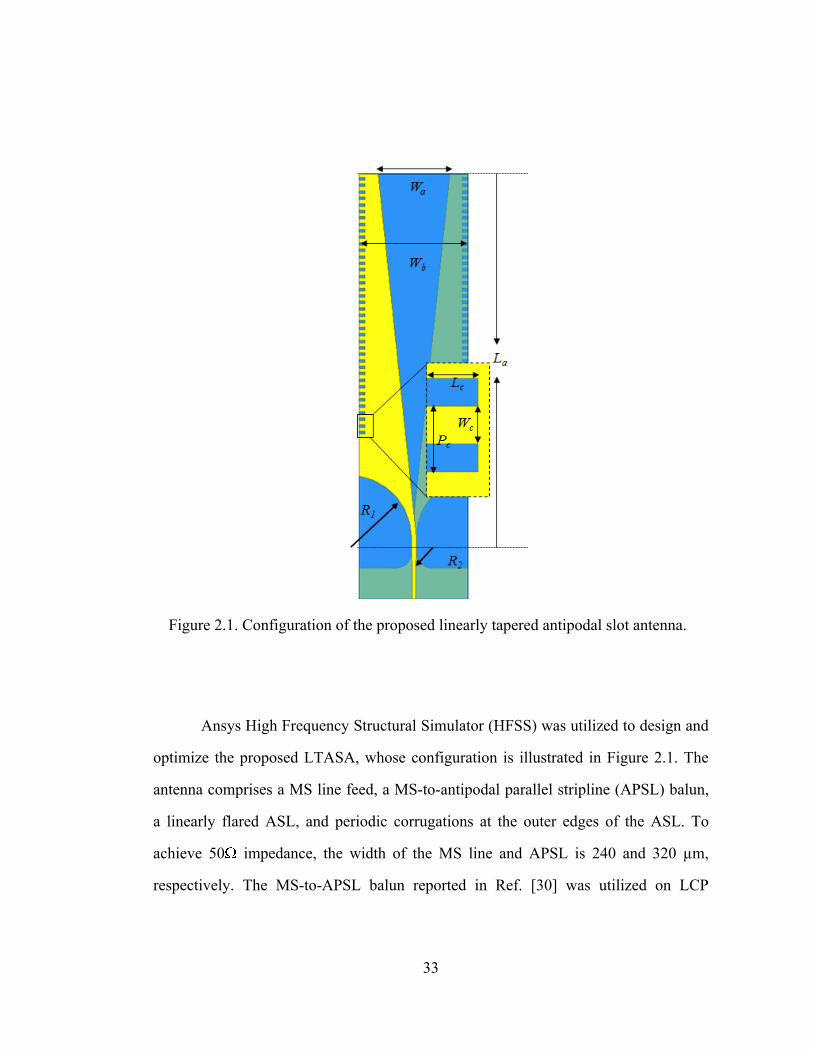
33
Ansys High Frequency Structural Simulator (HFSS) was utilized to design and
optimize the proposed LTASA, whose configuration is illustrated in Figure 2.1. The
antenna comprises a MS line feed, a MS-to-antipodal parallel stripline (APSL) balun,
a linearly flared ASL, and periodic corrugations at the outer edges of the ASL. To
achieve 50� impedance, the width of the MS line and APSL is 240 and 320 μm,
respectively. The MS-to-APSL balun reported in Ref. [30] was utilized on LCP
Figure 2.1. Configuration of the proposed linearly tapered antipodal slot antenna.

34
substrate, and scaled up to E-band to provide an ultra-wide band. The corrugations are
designed to further suppress the cross-polarization as well as the backward and side
lobes [28] [30]. Table 2.1 lists the optimized dimensions of the proposed LTASA.
The simulated S11 of the LTASA is shown in Figure 2.2, and it can be found
that the 10dB impedance bandwidth is from 48 to 110 GHz. Figure 2.3 illustrates the
simulated radiation patterns of the proposed antenna. Within the operational band, the
side lobes are less than -20 and -9 dB in the E- and H-planes, respectively, the
backward radiation is lower than -18 dB, and the cross-polarization is less than -15
dB. The simulated gain, 3dB beamwidths in the E- and H-planes, sidelobe, and cross-
polarization are listed in Table 2.2. It can be seen that the simulated gain is better than
17 dBi from 75 to 95 GHz, and the beamwidths are approximately symmetric in the E-
and H-planes at most of the frequencies. The radiation efficiency of the proposed
LTASA is higher than 95% from 70 to 110 GHz.
Table 2.1. Optimized dimensions of the proposed LTASA.
Parameters Dimensions (mm) La 23.5 Wa 5 Wb 7 R1 3 R2 1 Lc 0.38 Wc 0.24 Pc 0.42

35
Figure 2.2. Simulated S11 of the LTASA and measured S11 of the LTASAs integrated with a via-less CBCPW probe pad and a MS-to-SIW-to-waveguide transition.
Table 2.2. Simulated gain, beamwidth, first sidelobe, and cross-polarization of the proposed LTASA.
Freq. Gain Beamwidth 1st Sidelobe(H) Cross-Pol. 75 GHz 17.7 dB ±8.8º(E)/ ±13.5º(H) -11.5 dB -21.7 dB 80 GHz 17.5 dB ±9.1º(E)/ ±13º(H) -10.5 dB -18.3 dB 85 GHz 17 dB ±9.4º(E)/ ±12º(H) -9.7 dB -16.7 dB 90 GHz 17.1 dB ±8.8º(E)/ ±11.6º(H) -9.2 dB -16 dB 95 GHz 17 dB ±8.7º(E)/ ±11.2º(H) -8.9 dB -15.5 dB
Freq. and Pol. denote the frequency and polarization, respectively. E and H denote in the E-plane and H-plane, respectively.

36
(a) (b)
(c) (d)
(e)
Figure 2.3. Simulated and measured radiation patterns of the LTASA at (a) 75 GHz, (b) 80 GHz, (c) 85 GHz, (d) 90 GHz, and (e) 95 GHz.

37
2.3.2 Bandwidth Measurement
A G-S-G probe with an impedance of 50 � was utilized to characterize the
LTASA from DC to 110 GHz. To match the G-S-G mode of the probe, the MS feed is
terminated with a CBCPW probe pad [32], as shown in Figure 2.4. The termination
achieves low loss and low reflection at E- and W-bands, and its design will be
discussed in Section 3.2.2. In our measurement, the probe was calibrated with the
short-open-load-through (SOLT) method by using the on-wafer calibration substrate
Figure 2.4. Fabricated LTASAs with a via-less CBCPW probe pad and a MS-to-SIW-to-waveguide transition.

38
from GGB Industries Inc. The measured S11 is illustrated in Figure 2.2. An ultra-wide
band was demonstrated from 47 to 110 GHz, showing good agreement with simulated
data.
2.3.3 Far-field Measurement
At W-band, WR-10 waveguides are typically utilized to connect RF sources to
antennas due to their low attenuation. In order to integrate the LTASA with a
waveguide, a MS-to-SIW transition and a SIW-to-waveguide transition were designed.
The MS-to-SIW transition will be discussed in Section 3.3 of the next chapter. Here, I
present the SIW-to-waveguide transition, whose configuration is shown in Figure 2.5
(a). The transition linearly flares a 2.2mm wide SIW to a WR-10 waveguide with a
length of 25 mm. The insertion loss of its back-to-back transition is less than 1.6 dB
from 70 to 110 GHz, as illustrated in Figure 2.5 (b).
To characterize the antenna far fields, the proposed LTASA is terminated with
the aforementioned two transitions, as shown in Figure 2.4. The measured S11 of the
WR-10 fed LTASA is less than -12 dB at W-band, with the exception of the
frequencies near the waveguide’s cut-off, as illustrated in Figure 2.2.
2.3.3.1 Optically addressed far-field measurement system
Based on an optical upconversion approach [33], an optically addressed
antenna far-field measurement system is developed, whose configuration and
mechanism schematic are illustrated in Figure 2.6. Agilent programmable network
analyzer (PNA) E8361C integrated with millimeter wave head controller N5260A is
utilized as a W-band source, providing RF signals to a standard transmitting horn
antenna. The AUT is mounted on a rotation stage, and serves as a receiver. The

39
received RF signal is amplified, and then upconverted onto an optical carrier by using
a high-speed Lithium Niobate (LiNbO3) electro-optical (EO) phase modulator [34],
resulting in an upper and a lower optical sideband around the carrier frequency. The
amount of the energy of the sidebands, ���, can be quantified as [35]:
��� � ������ ������� �����
(a)
(b)
Figure 2.5. (a) Configuration of the SIW-to-waveguide transition, and (b) measured and simulated S-parameters of its back-to-back transition.

40
where ���� is the optical power into the modulator, ��� is the RF power received at the
antenna, �� is the gain of the LNA, � �� is the modulation efficiency of the phase
modulator.
The modulated signals are routed through optical fibers, which are preferable
for the measurement system setup due to their flexibility, low loss, small profile, and
light weight. These signals are then fed into a dense wavelength division multiplexing
(DWDM) optical filter to pass one of the sidebands while suppressing the carrier
Figure 2.6. Optically addressed far-field measurement system.

41
frequency and the other sideband. Next, a square-law detector (photodetector) is used
to convert this sideband to a photo-current. The weak current will be amplified using a
transimpedance amplifier (TIA). As a result, the voltage generated by the TIA can be
derived as [35]:
���� � �������� ������������ �����
where ���� is the gain of the TIA, and �� is the responsivity of the photodetector.
Then, the produced voltage is measured using National Instrument data acquisition
(NI DAQ) system.
2.3.3.2 Characterized radiation patterns and gain
Due to the limited bandwidth of the packaged LNA, the far fields of the
proposed LTASA were characterized from 75 to 95 GHz. The measured co- and cross-
polarized radiation patterns in the E- and H- planes are illustrated in Figure 2.3, which
are in good agreement with the simulated results. As the frequency increases from 75
to 95 GHz, the 3dB beamwidth in the E-plane remains approximately ±9º, and that in
the H-plane is reduced from ±13.5º to ±11º. The measured sidelobes are less than -20
and -9 dB in the E- and H-planes, respectively. As the frequency increases from 75 to
95 GHz, the cross-polarization increases from -20 dB to -15 dB, which is due to the
increasing substrate thickness in terms of wavelength.
To characterize the AUT’s gain, a standard pyramid horn with a gain of 15 dBi
was utilized as a reference to replace the LTASA and capture RF power. The insertion
losses of the MS-to-SIW and SIW-to-waveguide transitions were calibrated out so that
the actual gain of the LTASA could be acquired. The measured gain is higher than

42
16.5 dBi from 73 to 97 GHz, as illustrated in Figure 2.7. The discrepancy between the
measured and simulated results may be attributed to the integration tolerance.
2.4 Summary
In this chapter, I first discussed the system requirements for receiving antennas
in wireless systems, i.e., wireless communication, radar, and radiometry, and the
challenges for antenna design and measurement at W-band. Then, an UWB high-gain
LTASA on a 100μm thick LCP substrate for the E- and W-bands applications was
presented. The 10dB impedance bandwidth of the LTASA was demonstrated from 47
to 110 GHz. A sophisticated optical antenna far-field measurement system, based on
an optical upconversion, was developed to characterize the far-field properties of the
proposed LTASA. A high gain of 16.5-17.5 dBi, a narrow beamwidth of ±9º in the E-
Figure 2.7. Simulated and measured gain spectrum of the proposed LTASA.

43
plane, and a narrow beamwidth of around ±12º in the H-plane were demonstrated from
75 to 95 GHz. The proposed LTASA also achieves low side lobes and low cross-
polarization at E- and W-bands, and may have many applications in various wireless
systems.

44
TRANSITIONS IN MULTILAYER LCP SUBSTRATES
A transition is a passive transforming structure that connects circuit
components with different topologies. Its bandwidth determines the system bandwidth,
and its insertion loss may impact the system’s net gain and noise figure, which are
closely related to the dynamic range and sensitivity of a receiver.
3.1 Transmission Lines and Waveguides
Prior to the design of the transitions, the corresponding circuit components and
their topologies in the front-end receiving module should be determined. Typically, in
multilayer circuits, MS lines and CBCPWs are preferable in the surface layers due to
their low propagation loss and shielding ground, while striplines (SLs) and SIWs are
more appropriate in the inner layers due to their perfect layer-to-layer electrical
shielding. At the input and output interfaces, WR-10 air-filled rectangular waveguides
may be utilized for practical applications and measurement, and coplanar waveguides
(CPWs) may be desired for probing and integration with CPW-based EO modulators
[34]. In the traditional sense, MS lines, CPWs, CBCPWs, SLs, and rectangular
waveguides are the classic transmission components, and have been well investigated
[10]-[11] [14].
� MS line: a conducting strip separated from a ground plane by a dielectric substrate.
� CPW: a single conducting track printed onto a dielectric substrate, together with a
pair of return conductors distributed on both sides of the track.
Chapter 3

45
� CBCPW: a CPW with a ground plane underneath.
� SL: a thin conducting strip sandwiched between two parallel ground planes with
dielectric substrates as insulating materials.
� Rectangular waveguide: a metal pipe with a rectangular cross-section.
Recently, SIWs have been developed for printed circuits, which are waveguide-like
structures in a dielectric substrate by using two rows of metal vias to connect the top
and bottom parallel conductor layers. The cross-section and mode profile of these six
transmission components are illustrated in Figure 3.1. It can be seen that MS lines,
CPWs, and CBCPWs support quasi-TEM mode, SLs support TEM mode, and SIWs
and RWGs support TE10 mode.
Figure 3.1. Cross-section structure and fundamental mode profile of MS line, CPW, CBCPW, stripline, SIW, and rectangular waveguide.

46
As discussed in Section 1.4, LCP substrates with a multilayer topology are
proposed for the front-end receiving module, which is fabricated using commercial
state-of-the-art large-panel circuit print technologies [9]. At W-band, the dielectric
constant and loss tangent of LCP substrates are approximately 3.2 and 0.0045,
respectively. Thereby, using LCP substrates can minimize the dielectric loss of the
transmission lines. In addition, multilayer circuits can provide high desity, small size,
light weight, and low power consumption for the module as well as symmetric
substrates for the SLs and directional filters discussed in Chapter 5. Under the large-
panel fabrication standards [9], the minimum resolution of the circuit patterns is 50
μm, and the aspect ratio of the laser-drilled vias is 1.25:1. Table 3.1 lists the
fundamental mode, dimensions, and the corresponding propagation loss and
impedance at W-band of the five planar transmission components fabricated on a
100μm thick LCP substrate using the state-of-the-art large-panel circuit print
technologies. The MS line and SL have an impedance of 50 �, while the CPW and
CBCPW have higher impedances close to 70 �, which is limited by the fabrication
Table 3.1. Fundamental mode, dimensions, and simulated propagation loss and impedance at W-band of the five planar transmission components on a 100μm thick LCP substrate and WR-10 rectangular waveguide.
TL Mode Dimensions Loss (dB/cm) Impedance (�) MS line Quasi-TEM 246 μm 1-1.5 50
CPW Quasi-TEM 50 (gap)×100(signal) μm 0.9-1.3 66 CBCPW Quasi-TEM 50 (gap)×100(signal) μm 1-1.7 68 Stripline TEM 60 μm 1.6-2.4 50
SIW TE10 1.7 mm (width) 2 23 RWG TE10 2.54×1.27 mm 0.05
TL denotes transmission line.

47
resolution. The CPW has the minimum propagation loss, while the SIW has the
maximum propagation loss. To concurrently compensate for the propagation loss and
EMI between circuit components as well as mode and impedance mismatch, MS lines
are chosen for interconnection, SIWs and SLs are utilized to purify the guided modes
in the substrate, and CBCPWs and CPWs are used for integration and measurement. In
the following sections, I will present four ultra-wideband low-loss transitions between
these six transmission components for W-band applications.
3.2 CBCPW-to-Stripline Vertical Transition
As electronic devices become smaller and lighter, traditional single-sided and
double-sided printed circuits cannot satisfy increasing assembly densities due to their
limited space. As an alternative, multilayer circuits have received significant attention,
which can provide many advantages to RF/microwave circuit designers, i.e., high
density, small profile, hybrid integration, multi-function, low interconnection loss, and
good electrical shielding [36].
One of the most critical components in a multilayer circuit is the vertical
interconnection between different circuit layers. Conventional vertical transitions can
be classified in two categories: aperture-coupled transitions [37]-[40] and transitions
with vertical micro vias [40]-[42]. The former exhibit a bandpass behavior with a
bandwidth of 100% with respect to its center frequency, and the latter can offer a
wider bandwidth, but require more sophisticated manufacturing. Most of the vertical
transitions reported so far are designed for surface-to-surface connection [37]-[41],
which cannot be used for inner-layer applications. Additionally, these reported
transitions are designed at low frequencies, i.e., X-and K-band, and may not be

48
suitable at W-band. Reference [42] reported a transition that is able to operate up to 50
GHz. However, its insertion loss is higher than 3 dB at higher frequencies.
In this section, I present a CBCPW-to-stripline vertical transition in multilayer
LCP substrates, which can provide an insertion loss less than 2.5 dB over an ultra-
wide band from DC up to 78 GHz.
3.2.1 Transition Design
CBCPWs and SLs are commonly used transmission lines in multilayer RF
circuits, due to their superior advantages of good electrical shielding and low loss at
high frequencies. The former can be used for probing and external integration, and the
latter allows for the design of efficient and compact circuit topologies. As can be seen
in Figure 3.1, the CBCPW mode is the combination of a MS line mode and a CPW
mode, and the SL mode is a TEM mode. The proposed CBCPW-to-SL transition is
designed on two Rogers Ultralam3850 LCP substrates that consist of three metal
cladding layers. The thickness of each LCP layer and copper cladding is 50 and 9 μm,
respectively. The cross-section and layer-by-layer configuration of the transition are
illustrated in Figure 3.2 (a) and (b), respectively. The CBCPW is designed on the top
electrode layer, and the SL is sandwiched between the top and bottom LCP layers. To
achieve the transition, one blind-via and two through-vias are used to perpendicularly
connect the signal lines and grounds of the CBCPW and SL, respectively.
A 3-D finite element method (FEM) based electromagnetic solver, Ansys
HFSS, was used to design and optimize the CBCPW-to-SL transition and the
following transitions in this chapter. To attain an impedance of 50 �, the width of the
CBCPW’s signal line and gap is designed to be 110 and 70 μm, respectively, and the
width of the SL, Ls, is 60 μm. According to the circuit model of a vertical via [43], the

49
(a)
(b)
Figure 3.2. (a) Cross section and (b) layer-by-layer configuration and dimensions of the CBCPW-to-SL transition.

50
parasitic capacitance between the vias barrel and parallel grounds may contribute to
parallel-plane evanescent wave. To investigate the impact of the blind via to the
performance of the transition, the diameter, Dv, was varied from 80 to 120 μm, and the
pitch between the signal and ground vias, Pv, was swept from 0.4 to 0.5 mm. The
simulated S-parameters for the tolerance analysis are illustrated in Figure 3.3 (a) and
(b). It can be seen that slightly sweeping the diameter and pitch of the vias does not
change the transition performance significantly. The insertion loss and reflection
become enhanced as the frequency increases, which is due to the fact that the
evanescent wave is easier to be excited at high frequencies. A larger blind via could
smooth the reflection response, but can also provide higher capacitance at the
frequencies over 80 GHz. Also, a larger blind via represents larger ring [9], which
could lead to additional impedance mismatch between the vias and transmission lines.
As illustrated in Figure 3.3 (b), increasing the pitch between the signal and ground
vias can suppress the mutual coupling between the vias, but also increases the
insertion loss at high frequencies due to the inductance mismatch. To concurrently
optimize the performance of the transition and avoid touching the fabrication limit, the
diameter of the signal via is chosen as 100 μm, and the pitch between the signal and
ground vias is chosen as 0.5 mm. The diameter of the ground vias is chosen as 240 μm,
since they are not dimension-sensitive.
3.2.2 Measurement
3.2.2.1 System set-up
As discussed in Section 1.2, the traditional SMCs for device integration are
lossy and expensive at W-band. As an alternative, G-S-G probes are typically utilized

51
to couple signals into and out of the DUTs at high frequencies, which have a
characteristic impedance of 50 � and provide a CPW mode. In the measurement set-
up, the probes on probe stations were integrated with Agilent PNA E8361C and mmW
(a)
(b)
Figure 3.3. Simulated S-parameters of a CBCPW-to-SL transition: (a) tolerance analysis of the diameter of the blind via, and (b) tolerance analysis of the pitch between the blind and through vias.

52
head controller N5260A. Then, the two probes were calibrated with CS-5 calibration
substrate from GGB Industries Inc. using SOLT method. The same system set-up and
calibration method will be utilized in the following sections and chapters without
special clarification.
3.2.2.2 Back-to-back transition
To demonstrate the proposed CBCPW-to-SL transition, its back-to-back
transition was designed and fabricated, which consists of one SL and two CBCPWs, as
(a)
(b)
Figure 3.4. (a) Fabricated CBCPW-to-SL-to-CBCPW transition, and (b) cross-section cut of the fabricated back-to-back transition.

53
shown in Figure 3.4 (a). Choosing two CBCPWs is for the consideration of probing.
The fabricated CBCPW’s signal line width is reduced to 105 μm, while its gap width
is increased to 80 μm due to the fabrication tolerance. The length and width of the SL
are 3 mm and 58 μm, respectively. The cross-section cut of the transition is shown in
Figure 3.4 (b). It can be seen that the laser-drilled vias are slightly tapered cylinders.
The diameter of the blind via varies from 93 μm to 100 μm, and that of the through
vias varies from 220 μm to 240 μm.
The measured S-parameters of the back-to-back transition are illustrated in
Figure 3.5, showing good agreement with the simulated results. The insertion loss is
1.8 dB at 60 GHz and less than 2.5 dB up until 78 GHz, and the reflection remains less
than -10 dB from DC up to 78 GHz. The slight discrepancy between the simulated and
Figure 3.5. Simulated and measured S-parameters of the back-to-back transition with a 3 mm long SL.

54
measured data may be attributed to fabrication tolerances and probe positioning
uncertainty.
3.3 MS-to-SIW Transition
Recently, substrate integrated waveguides have been developed to adapt
traditional rectangular waveguides into planar substrates with existing PCB
technologies. SIWs are typically fabricated by using two rows of conducting vias
connecting two parallel grounds [44], which preserve most of the rectangular
waveguides’ advantages, i.e., high-power handling capability and perfect electrical
shielding, and can further provide low profile, light weight, and simple integration.
Typically, the loss of a SIW is higher than that of a hollow rectangular waveguide due
to the dielectric loss of the substrate material. A carefully designed SIW can only
support TE10 mode within a wide spectrum and, therefore, can be utilized to purify the
guided mode and improve the module’s EMC. Generally, SIWs can be fed by using
MS lines, CPWs, and CBCPWs [44]. As discussed in Section 3.1, MS lines are
utilized to interconnect different circuit components in the receiving module due to
their relatively low propagation loss and shielding ground. Thereby, an efficient
transition from MS line to SIW is desired in the proposed module.
As can be seen in Figure 3.1, the MS line mode is a quasi-TEM mode, and the
SIW mode is a TE10 mode. These two modes have similar mode profiles in their
substrates. Herein, a transition between a MS line and a SIW can be achieved directly
by connecting the MS line’s signal line to the SIW’s top ground and the MS line’s
ground to the SIW’s bottom ground. To date, several broadband MS-to-SIW
transitions have been reported in planar or multilayer substrates [44]-[46] at
microwave frequencies, which, however, may not be migrated to high frequencies, e.g.,

55
95 GHz. As the frequency increases to W-band, due to the limited commercial
fabrication resolution of the micro vias discussed in Section 1.2, the pitch between
vias becomes electrically ‘large’ in terms of wavelength, which may introduce
additional leakage loss at such high frequencies. Thus, the MS-to-SIW transitions
reported at microwave frequencies have to be validated at W-band.
In this section, I present a planar MS-to-SIW transition on a thin film LCP
substrate and demonstrate its application in commercial printed circuits. The proposed
transition achieves a low loss of less than 1.6 dB and an ultra-wide bandwidth from 60
to 110 GHz.
3.3.1 Transition Design
To minimize the impact of multilayer lamination tolerance, the MS line and
SIW are designed in a core LCP layer. The thickness of this core layer is chosen as
100 μm to minimize the propagation loss of the MS line and SIW. The proposed MS-
to-SIW transition is a linear taper between a MS line and a SIW, whose configuration
is illustrated in Figure 3.6. The width of the SIW is denoted as � , and the
corresponding effective width is:
���� � � ���
��� ����
where � and � are the diameter and pitch of the vias, respectively. The corresponding
cut-off frequency of the SIW can be calculated using the following formula [44]:
� ��
�������� ����
where � is the speed of light in free space, and �� is the dielectric constant of the
substrate. Limited by the fabrication aspect ratio (1.25:1) and thickness of the
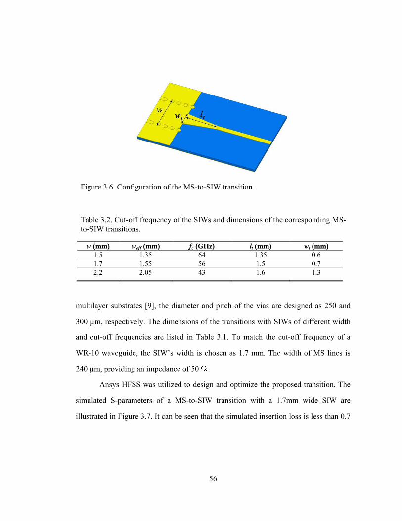
56
multilayer substrates [9], the diameter and pitch of the vias are designed as 250 and
300 μm, respectively. The dimensions of the transitions with SIWs of different width
and cut-off frequencies are listed in Table 3.1. To match the cut-off frequency of a
WR-10 waveguide, the SIW’s width is chosen as 1.7 mm. The width of MS lines is
240 μm, providing an impedance of 50 �.
Ansys HFSS was utilized to design and optimize the proposed transition. The
simulated S-parameters of a MS-to-SIW transition with a 1.7mm wide SIW are
illustrated in Figure 3.7. It can be seen that the simulated insertion loss is less than 0.7
Figure 3.6. Configuration of the MS-to-SIW transition.
Table 3.2. Cut-off frequency of the SIWs and dimensions of the corresponding MS-to-SIW transitions.
w (mm) weff (mm) fc (GHz) lt (mm) wt (mm) 1.5 1.35 64 1.35 0.6 1.7 1.55 56 1.5 0.7 2.2 2.05 43 1.6 1.3

57
dB, and the reflection is less than -15 dB at W-band. The simulated cut-off frequency
of the SIW is 57.6 GHz, which is slightly higher than the calculated one in Table 3.1.
3.3.2 Measurement
3.3.2.1 CBCPW probe pad
At high frequencies, i.e., W-band, G-S-G probes are typically utilized to
measure the RF components. To match the modes between the MS line and G-S-G
probe, a CBCPW probe pad was designed to terminate the MS lines, as illustrated in
Figure 3.8 (a). In the HFSS model, the designed width of the CBCPW’s signal line
and gap is 80 and 50 μm, respectively, and the taper length is 0.2 mm. For the
fabricated device, the width of the signal electrode reduces to 70 μm, while the gap
between the signal line and ground increases to 60 μm due to the fabrication tolerance.
Figure 3.7. Simulated S-parameters of a MS-to-SIW transition (� = 1.7 mm).

58
This overetching enlarges the corresponding impedance of the CBCPW up to around
80 �. The probing position is chosen right at the end of CBCPW to minimize the
mismatch.
(a) (b)
(c)
Figure 3.8. (a) Configuration of a CBCPW probe pad and its back-to-back transition,(b) simulated and measured S-parameters of a 5mm long MS line terminated with a pair of probe pads, and (c) calculated propagation loss of a MS line and insertion loss of a pair of probe pads.
59
To characterize the insertion loss of the proposed probe pads, back-to-back
structures including two CBCPW probe pads and MS lines with different length, are
fabricated and measured. The simulated and measured S-parameters of a 5mm long
MS line with a pair of probe pads are illustrated in Figure 3.8 (b). The loss of the MS
line can be calculated by dividing the S21 discrepancy of the back-to-back structures
by their length difference. Then, the insertion loss of a pair of CBCPW probe pads can
be derived by subtracting the loss of the MS line from the total loss of a back-to-back
transition. More than twenty devices were measured to obtain robust loss curves,
which are illustrated in Figure 3.8 (c). The propagation loss of the MS line is less than
0.14 dB/mm from 50 GHz to 110 GHz, showing good agreement with the simulated
data in Table 3.1, and the loss of a pair of probe pads is lower than 1.4 dB at W-band.
The relatively large ripples from 95 to 110 GHz may be attributed to the spectrum
edge error of calibration and probing position uncertainty. The designed CBCPW
probe pads will be utilized in the measurements of the devices with MS line feed in
the following sections and chapters.
3.3.2.2 Back-to-back transition
To validate the design of the proposed transition, a MS-to-SIW-to-MS
transition terminated with a pair of CBCPW probe pads was designed and fabricated.
The length and width of the SIW is 5 mm and 1.7 mm, respectively, and the length of
MS lines is 1.5 mm, as illustrated in Figure 3.9 (a). The measurement set-up and
calibration method discussed in Section 3.2.2 were utilized for this test. Figure 3.9 (b)
illustrates the measured and simulated S-parameters of the back-to-back structure,
revealing reasonable agreement. The measured insertion loss is less than 1.6 dB at W-
band, and the measured reflection is less than -13 dB within the working spectrum. It
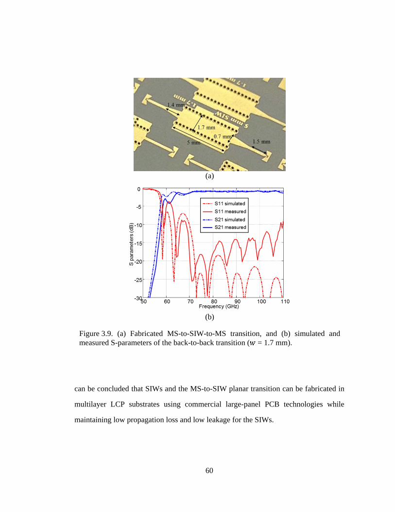
60
can be concluded that SIWs and the MS-to-SIW planar transition can be fabricated in
multilayer LCP substrates using commercial large-panel PCB technologies while
maintaining low propagation loss and low leakage for the SIWs.
(a)
(b)
Figure 3.9. (a) Fabricated MS-to-SIW-to-MS transition, and (b) simulated and measured S-parameters of the back-to-back transition (� = 1.7 mm).

61
3.4 SIW-to-Waveguide Transition
Hollow rectangular waveguides (RWGs), one of the earliest transmission
components for microwave signal transportation, have been widely utilized in the
microwave and mmW systems due to their low loss, high power handling capability,
and perfect electrical shielding. However, RWGs are bulky and heavy, and, thereby,
not suitable for high-density and weight-constrained applications [25] [44].
Alternatively, SIWs have gained tremendous interests in these applications [44],
which preserve the traditional RWGs’ advantages, and can achieve low profile, light
weight, and friendly packaging. So far, many efforts have been done to investigate
SIW-to-rectangular waveguide transitions [46]-[54]. According to the mechanism used,
these transitions can be classified into two categories: slot coupled transitions on the
broadside [46]-[47] and travelling-wave transitions in the propagation direction [48]-
[54]. The former utilize one or two slots on the SIW’s broadside wall to couple signal
into RWG. However, their bandwidth is typically several percent due to the SIWs’
high quality factor. The latter are typically achieved by using tapered housings [48]-
[51] or fin-lines [52]-[54] to gradually match the TE10 modes of the SIWs and RWGs
in the wave propagation direction, and can achieve broad bandwidth at a cost of circuit
footprint.
Recently, SIWs have been investigated in multilayer circuitry [25] due to their
aforementioned advantages. However, it should be noted that all the reported SIW-to-
RWG transitions [46]-[54] are designed on a single layer substrate, which may not be
applicable in the multilayer substrate. On one hand, the broadside slot coupled
transitions may have limited applications due to their narrow bandwidth and large
profile in the broadside direction. On the other hand, for the travelling-wave
transitions, the substrate thickness becomes electrically ‘thick’ in terms of wavelength
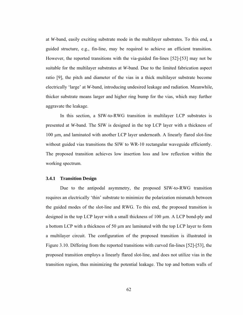
62
at W-band, easily exciting substrate mode in the multilayer substrates. To this end, a
guided structure, e.g., fin-line, may be required to achieve an efficient transition.
However, the reported transitions with the via-guided fin-lines [52]-[53] may not be
suitable for the multilayer substrates at W-band. Due to the limited fabrication aspect
ratio [9], the pitch and diameter of the vias in a thick multilayer substrate become
electrically ‘large’ at W-band, introducing undesired leakage and radiation. Meanwhile,
thicker substrate means larger and higher ring bump for the vias, which may further
aggravate the leakage.
In this section, a SIW-to-RWG transition in multilayer LCP substrates is
presented at W-band. The SIW is designed in the top LCP layer with a thickness of
100 μm, and laminated with another LCP layer underneath. A linearly flared slot-line
without guided vias transitions the SIW to WR-10 rectangular waveguide efficiently.
The proposed transition achieves low insertion loss and low reflection within the
working spectrum.
3.4.1 Transition Design
Due to the antipodal asymmetry, the proposed SIW-to-RWG transition
requires an electrically ‘thin’ substrate to minimize the polarization mismatch between
the guided modes of the slot-line and RWG. To this end, the proposed transition is
designed in the top LCP layer with a small thickness of 100 μm. A LCP bond-ply and
a bottom LCP with a thickness of 50 μm are laminated with the top LCP layer to form
a multilayer circuit. The configuration of the proposed transition is illustrated in
Figure 3.10. Differing from the reported transitions with curved fin-lines [52]-[53], the
proposed transition employs a linearly flared slot-line, and does not utilize vias in the
transition region, thus minimizing the potential leakage. The top and bottom walls of

63
the SIW deviate with an odd symmetry to feed the slot-line. The diameter and pitch of
the vias for the SIW is 250 and 300 μm, respectively. Then, the slot-line is linearly
flared out and inserted into a WR-10 waveguide. By using this linear transition, the E-
field of the SIW will be rotated 90º to excite the TE10 mode of the RWG.
To optimize the transition, 3-D full-wave models are designed and simulated in
Ansys HFSS, as illustrated in Figure 3.10. The width of the SIW is chosen as 1.6 mm,
Figure 3.10. Configuration and dimensions of the SIW-to-WG transition in multilayer LCP substrates.

64
providing the same cut-off frequency as the WR-10 waveguide. The length of the
flared slot-line is 7 mm, and the distance between the edges of the slot-line and SIW is
depicted as L. The bond-ply and bottom LCP introduce index asymmetry between the
top and bottom electrodes of the antipodal slot-line and, thereby, may excite a parasitic
mode at high frequencies. The fundamental and parasitic modes of the proposed
(a)
(b) (c)
Figure 3.11. (a) Propagation and cross-section of the fundamental and parasitic modes of the proposed SIW-to-WG transition, and simulated (b) S11 and (c) S21 of the transition with varying L at W-band.

65
transition are illustrated in Figure 3.11 (a). It can be found that this mode is confined
between the top and bottom electrodes of the antipodal slot-line. Therefore, increasing
L can push the parasitic mode to high frequencies. The simulated S-parameters of the
transition with sweeping L are illustrated in Figure 3.11 (b). At L = 0.4 mm, the
parasitic mode occurs at 117 GHz, beyond W-band. Further increasing L may increase
the mode mismatch between the slot-line and SIW, thus enlarging the loss of the
proposed transition significantly.
3.4.2 Measurement
To characterize the proposed transition, a RWG-to-SIW-to-RWG transition
was designed and fabricated, as illustrated in Figure 3.12 (a). The length of the SIW is
designed as 20 mm, providing enough space for the registration posts. A metallic
housing is carefully designed to provide WR-10 waveguide input and output with a
standard flange. In the measurement set-up, the external WR-10 waveguides were
integrated with Agilent N5260 mmW heads and PNA E8361C and calibrated with
SOLT method and W11644A calibration kit. Then, they were integrated with the
packaged back-to-back transition and characterize its S-parameters.
The measured and simulated S-parameters of the back-to-back transition are
illustrated in Figure 3.12 (b). The measured reflection is less than -11 dB, and the
insertion loss is less than 1.9 dB from 70 to 110 GHz, showing good agreement with
the simulated data. It should be noted that to precisely reveal the insertion loss of the
back-to-back transition, the propagation loss of the SIW is eliminated, which can be
calculated by using the method to calculate the insertion loss of probe pads discussed
in Section 3.3.2. Both the simulated and measured S-parameters reveal that the
proposed SIW-to-RWG transition does not excite substrate modes at W-band.

66
(a)
(b)
Figure 3.12. (a) Fabricated waveguide-to-SIW-to-waveguide transition with metal housing, and (b) simulated and measured S-parameters of the back-to-back transition.

67
3.5 MS-to-CPW Transition
Coplanar waveguide (CPW) is one type of transmission line whose signal and
ground conductors are in the same plane, namely, on the top surface of the dielectric
substrate [10]. Traditionally, CPWs are widely used in monolithic microwave/
millimeter integrated circuits (MMICs) due to the simple mounting of lumped
components. In this case, CPWs are also preferable in the circuits of MMIC carriers to
provide the same mode for the MMICs’ integration. At mmW frequencies, CPWs
typically provide lower propagation loss than the other transmission lines due to their
unique mode profile and relatively low dielectric loss, as depicted in Figure 3.1 and
Table 3.1. However, they are not suitable in multilayer circuits due to their poor layer-
to-layer isolation. In the proposed front-end receiving module, CPWs can be utilized
for the G-S-G probing in the measurement and integration with amplifiers or EO
modulators. As mentioned in Section 3.1, MS lines are chosen as the transmission
lines for interconnection. Therefore, an efficient transition from MS line to CPW is
important for the proposed module.
Recently, many MS-to-CPW transitions have been reported in single or
multilayer substrates [55]-[63]. The transitions in a single-layer substrate are mainly
designed for the input/output probe pads in RFICs or MMICs [55]-[57], typically
having compact dimensions at a cost of relatively high insertion loss. The reported
multilayer transitions are designed for surface-to-surface connection by using micro
vias [58]-[59] or coupling slots [60]-[61]. However, these transitions are not suitable
for the proposed module, where both the MS line and CPW are on the top circuit layer.
To achieve an ultra-wide bandwidth, reference [63] used a CBCPW to mitigate the
mode mismatch between the MS line and CPW [63] at Ka-band. However, it should
be noted that most of the reported transitions [55]-[63] are designed at low frequencies,

68
such as Ku- and K-bands, and may not be applied to W-band due to the fabrication
limits discussed in Section 1.2.
In this section, I present a planar MS-to-CPW transition in a thin-film LCP
substrate at W-band using a CBCPW as an intermedium between the MS line and
CPW. The proposed transition can provide low loss, low reflection, and ultra-wide
bandwidth.
3.5.1 Transition Design
As can be seen in Figure 3.1, the MS line mode and CPW mode are quasi-
TEM modes. The former is mainly confined underneath the metal strip within the
substrate, while the latter is close to the surface of the substrate. Combining these two
modes can form a CBCPW mode. Thereby, a broadband MS-to-CPW transition can be
achieved naturally by cascading a MS-to-CBCPW transition and a CBCPW-to-CPW
transition, whose configuration is illustrated in Figure 3.13. To minimize the
propagation loss of the MS line and CBCPW, the transition is designed on a 100 μm
thick LCP substrate. The width of MS line is chosen as 240 μm, providing an
impedance of 50 �, and the width of the signal line and gap of the CBCPW and CPW
are 110 μm and 60 μm, respectively, which is limited by the commercial large-panel
PCB fabrication standards discussed in Section 3.1. The corresponding impedance of
CBCPW and CPW is approximately 70 �, as depicted in Table 3.1. To transition a
MS line to a CBCPW, the signal line of the MS line is gradually narrowed down, and
two grounds connected to the bottom ground with through vias are added on the top
circuit layer. To achieve a CPW, a linearly tapered notch is introduced in the
CBCPW’s bottom ground to push the electrical fields lifting up towards the substrate
surface. A 3-D full-wave model of the proposed transition was designed and simulated

69
by using Ansys HFSS. The optimized dimensions of the transition are depicted in
Figure 3.13. The length of the CBCPW is 0.8 mm, the length of the linear taper
between the CBCPW and MS line is 0.8 mm, and the length and width of the notch in
the bottom ground are 1.2mm and 0.8 mm, respectively. Figure 3.14 illustrates the
simulated S-parameters of the proposed transition. It can be seen that the insertion loss
is less than 0.8 dB, and the reflection is less than -15 dB from 70 to 110 GHz.
3.5.2 Measurement
The measurement system set-up and calibration method discussed in Section
3.2.2 are utilized to characterize the fabricated MS-to-SIW transition. The MS line is
terminated with a low-loss CBCPW probe pad presented in Section 3.3.2. Figure 3.14
(a) illustrates the fabricated MS-to-SIW transition. It can be seen that the overetching
is approximately 5 μm. In the measurement, the input and output probes are launched
Figure 3.13. Configuration of the MS-to-CPW transition.

70
on the CBCPW probe pad and CPW, respectively, to couple the RF signal into and out
of the transition. The measured S-parameters of the MS-to-CPW transition are
illustrated in Figure 3.14 (b). It can be seen that the insertion loss and return loss are
(a)
(b)
Figure 3.14. (a) Fabricated MS-to-CPW transition with a CBCPW probe pad, and (b) simulated and measured S-parameters of this transition.

71
less than -1 dB and -13.5 dB at W-band, respectively. Again, the discrepancy between
the simulated and measured S-parameters may be attributed to the probe pad and
fabrication tolerance.
3.6 Summary
In this chapter, I first discussed the transmission components desired in the
multilayer LCP based front-end receiving module, including MS lines, CBCPWs,
CPWs, SLs, RWGs, and SIWs. MS lines are utilized for interconnection, CBCPWs
and CPWs are designed for the integration with MMICs and EO modulators as well as
probing, and SIWs and SLs can be used to suppress the undesired substrate modes. In
Section 3.2, a CBCPW-to-SL vertical transition is presented, which is achieved using
one blind via connecting the signal lines and two through vias connecting the grounds
in multilayer substrates. Then, a planar MS-to-SIW transition using a linear taper was
presented in Section 3.3, and a SIW-to-RWG transition in multilayer substrates was
presented in Section 3.4. The latter transition is achieved using a linearly flared
antipodal slot-line without guided vias in the transition region, and, thereby, can
minimize the potential leakage. In Section 3.5, I presented a planar MS-to-SIW
transition for probing and integration purposes, which comprises a MS-to-CBCPW
transition and a CBCPW-to-CPW transition. These four transitions can provide low
loss and low reflection within an ultra-wide band covering the frequencies at W-band.

72
MULTI-CHIP MODULE INTEGRATION AND PACKAGE
W-band frequencies within the millimeter wave spectrum have gained
tremendous interest in various applications, including vehicle collision avoidance
radar, gigabyte data rate communication, local wireless network, and passive and
active imaging [25] [44], etc. To cover a large dynamic range and achieve high
detection sensitivity, high-gain and low-noise figure receiving modules are of great
interest, which typically comprise multiple microwave/mmW monolithic integrated
circuits, such as low noise amplifiers and power amplifiers. Also, other system
constraints, i.e., high density, low profile, low loss, and light weight [63], also need to
be carefully considered in these applications, which typically can be achieved by using
multilayer circuitry. However, as the frequency and packaging density increases, loss,
reflection, and stray radiation in the form of crosstalk and package moding become
critical limiting factors for multi-chip modules (MCMs) [64]. Traditional packaging
technologies for the single-chip and low gain modules may not be suitable for high
gain MCMs at W-band.
Recently, system-on-package (SOP) technologies have received significant
attention in module integration and packaging at W-band [65]-[69]. However, most
papers reported so far investigate single-chip modules (SCMs) with a fairly low gain
of less than 18 dB using flip-chip bonding techniques. References [65] and [66] utilize
traditional substrates, silicon and ceramic, as the MMIC carriers, respectively.
However, these two kinds of substrates cannot be stacked to achieve multilayer
Chapter 4

73
circuits and, thereby, are not able to provide high density for the components and
assembly in a module. As an alternative, LCP is an ideal material for multilayer circuit
at mmW frequencies, and has been investigated as MMIC carriers in Ref. [67]-[69].
Nevertheless, the integration of MMICs on LCP substrates using traditional flip-chip
or wire bonding is challenging due to the large permittivity mismatch between the
LCP and MMICs’ substrates. Typically, flip-chip bonds require CPWs or CBCPWs as
the feed lines for the MMICs. However, due to the low permittivity of the LCP
substrate, it is critical to fabricate a 50 � CPW or CBCPW with a similar mode profile
to that of the MMICs’ probe pads at W-band using the commercial large-panel circuit
print technologies [9]. Customized thin metal claddings [67]-[69] may be applied to
the LCP substrate to improve fabrication resolution and achieve compact CPWs or
CBCPWs. However, thin metal cladding increases the cost significantly, especially for
large-panel and large-quantity applications. In addition, wire bonding is more versatile,
and can be utilized for CPW, CBCPW, and microstrip (MS) line feeds. References
[70]-[72] investigated the wire-bonded modules on LCP substrates at low frequencies,
i.e., Ka-band. However, these feeding transmission lines suffer from the same mode
mismatch due to the aforementioned permittivity mismatch. Besides, as the frequency
increases, the inductance of the traditional wire bond increases significantly, thereby
introducing additional impedance mismatch as well.
In this chapter, I present the integration and packaging techniques for high-
gain MCMs in multilayer LCP substrates and propose a 50 dB gain double-LNA
module at W-band. The proposed module employs a four-circuit layer LCP substrate
as a MMIC carrier, which was fabricated on 12×18 inch panels using commercial
state-of-the-art large-panel circuit print technologies [9]. In the proposed MCM, RF

74
components and bias circuits are distributed in different layers in order to achieve
higher density. To efficiently integrate the LNAs with the MS line feeds, V-shape wire
bonds are designed as a substitute to the traditional wire bonds. The proposed MCM
achieves high gain, low NF, and linear phase at W-band. This chapter is organized as
follows. In Section 4.1, the utilized LNA will be discussed. Then, the multilayer LCP
carrier and V-shape wire bond will be depicted in Section 4.2 and 4.3, respectively. In
Section 4.4, I will present the developed single-LNA and double-LNA modules. In
Section 4.5, the package technologies will be discussed.
4.1 NG ALP283 Low Noise Amplifier
To achieve high gain and low NF, the state-of-the-art Northrop Grumman (NG)
ALP283 LNA was chosen for the proposed modules, which can provide a high gain of
30 dB and a low NF of less than 2.5 dB at W-band [73]. The configuration of the LNA
is illustrated in Figure 4.1 (a). It is 2 mm long and 0.8 mm wide, and is fabricated on a
75μm thick indium phosphide (InP) substrate. The pitch between the signal and
ground bond pads is 90 μm. Figure 4.1 (b) shows the on-chip measured gain of the
LNA. It can be found that the measured gain is higher than 30 dB from 80 to 100
GHz. The active input and output impedances of the LNA can be extracted from the
on-chip measured S-parameters as follows [11]:
��� ��� � ������ �� � ����
���� � ���
�� ����
���� � ���
�� ����
���� � ���

75
��� ��� � ������ �� � ����
���� � � �
�� � �� ���� ���� ���� � ���
��� � � ����
��� � ��� ���
���� � ��� ����
� � ��� � ���
(a)
(b) (c)
Figure 4.1. (a) Top view, (b) measured on-chip gain, and (c) calculated input and output impedances of the NG ALP283 LNA.

76
where ��� and ��� (m = 1, 2 and n = 1, 2) are the S- and Z-parameters, respectively;
Z0, ZL, and ZS are the characteristic impedance, load impedance, and source
impedance, respectively, and equal 50 � in the on-chip measurement. The calculated
input and output impedance of the LNA are illustrated in Figure 4.1 (c). It can be seen
that the calculated active impedance of the LNA is approximately 50 � at most of the
frequencies at W-band. In this case, to minimize impedance mismatch, 50�
transmission lines are preferred to feed the LNAs.
4.2 Multilayer-LCP MMIC Carrier
Multilayer printed circuits are superior to the traditional single-sided and
double-sided circuits due to their high density, low connection loss, and multi-
function capability [74]. At mmW frequencies, LCP is a promising material for the
multilayer application due to its low loss, low dielectric constant, low water absorption,
and available thicknesses down to 25 μm [8] [23]. The dielectric constant and loss
tangent of LCP are approximately 3.2 and 0.004, respectively, at W-band [8]. Herein, a
multilayer LCP substrate is chosen as the LNA’s carrier, consisting of three LCP
layers and four circuit layers, as illustrated in Figure 4.2. The thickness of the top LCP,
inner bond-ply, and bottom LCP is 100 μm, 50 μm, and 50 μm, respectively. The RF
components, including LNAs, MS line feeds, and isolation structures, are designed in
the top two circuit layers to minimize the impact of multilayer lamination tolerance,
while the LNA bias and digital control circuits are designed in the bottom two layers,
achieving high density and multi-function for the proposed module.
For the consideration of large quantity production, the proposed multilayer
LCP carriers are fabricated using the commercial state-of-the-art large-scale circuit
print technologies with a minimum fabrication resolution of 50 μm for circuit patterns

77
[9]. Generally, CBCPWs and MS lines are the two most prolific transmission lines in
multilayer circuits due to their perfect layer-to-layer electrical shielding [74]-[75].
However, the CBCPWs are not suitable for the LNA integration on LCP substrates.
On a 100μm thick LCP substrate, in order to achieve a 50� CBCPW with the
commercial fabrication standards, the signal width of the CBCPW has to be as large as
200 μm, and the corresponding signal-to-ground pitch is much larger than that of the
LNA bond pads (90 μm), leading to strong mode mismatch. To this end, 50� MS
lines with a width of 240 μm are chosen to feed the LNAs with carefully designed V-
shape wire bonds, which will be presented in the next subsection. To probe the module,
a pair of CBCPW probe pads presented in Section 3.3.2 are employed to terminate the
MS lines.
Figure 4.2. Layer-to-layer circuit schematic of the multilayer LCP carrier.

78
4.3 V-Shape Wire Bond
Flip-chip [76] and wire bonding [77] are the two main chip-level integration
techniques at high frequencies. The former addresses low inductance and typically
requires CPWs or CBCPWs as feed lines [76]. However, CPWs are not suitable for
multilayer circuitry due to their poor layer-to-layer isolation, and CBCPWs suffer
from the aforementioned mode dimension mismatch between the LCP and LNAs as
well as inherent mode mismatch due to the fact that CBCPW mode is a combination of
CPW and MS line modes. Alternatively, wire bonding can be adapted to most
transmission lines, i.e., MS lines, CPWs, and CBCPWs. The inductance of a wire
bond is typically larger than a flip-chip bond at high frequencies, and can be estimated
by the following formula [14]:
� � ��� � � � �� � � � � � � �� � � � ���� ����� where l and d are the length and diameter of the wire bond, respectively, and h is the
height of the wire bond with respect to the ground. It can be found that reducing h and
l can decrease the inductance of wire bonds.
The utilized NG ALP283 LNA is designed for wire bond integration. To
minimize the inductance of the wire bond, the LNA chip is embedded in a laser-drilled
pocket in the top LCP layer, as illustrated in Figure 4.3 (a), reducing h in Equation
(4.8). The empirical thickness of the conductive silver epoxy for the LNA adhering is
approximately 20 μm. Thus, the LNA will be approximately level with the MS line
feeds on the LCP substrate.
To match the mode profiles between the MS lines on the LCP substrate and
LNA as well as further reduce the wire bond’s inductance, V-shape wire bonds are

79
designed and utilized for the LNA integration, as illustrated in Figure 4.3 (a). HFSS is
utilized to construct and simulate the 3-D full-wave models of the proposed V-shape
wire bond as well as a traditional single wire bond for comparison. The gap between
(a)
(b) (c)
Figure 4.3. (a) Configuration of the V-shape wire bond and traditional single wire bond, (b) simulated S-parameters of these two wire bonds as well as the circuit module (CM) of the V-shape wire bond, and (c) calculated input and output impedances of the wire bonds.

80
the LNA and MS line is 130 μm, and the length, L, and height, H, of the wire bond are
220 and 20 μm, respectively. The diameter of the wire bond is 25 μm, and the flared
pitch, W, of the V-shape wire bond is 150μm. In the simulation, the wave ports are de-
embedded to the wire bonding positions, as shown in Figure 4.3 (a). The simulated S-
parameters of the two wire bonds are illustrated in Figure 4.3 (b). It can be seen that
the proposed V-shape wire bond provides much lower insertion loss and reflection
than the traditional single wire bond. Tolerance analysis has been done to the V-shape
wire bond’s length (L) from 200 to 240 μm, flared width (W) from 130 to 170 μm, and
height (H) from 10 to 30 μm, revealing little degradation to the performance of the
proposed wire bond. Using Equations (4.1)-(4.7), the input and output impedances of
these two wire bonds were calculated, as illustrated in Figure 4.3 (c). It can be seen
that the proposed V-shape wire bond has a resistance of around 50 � and a low
reactance of less than 10 � from 70 to 110 GHz.
To better understand the proposed V-shape wire bond, its equivalent circuit
model was designed, as illustrated in Figure 4.4. According to the curvature, the low
profile V-shape wire bond can be divided into three parts [77], i.e., region A on the
LCP substrate, region B in free space, and region C on the LNA. LAs and LAw represent
the inductances of the MS line and wire bond in region A, respectively; LCs and LCw
are the inductances of the MS line and wire bond in region C, respectively. CA and CC
are the capacitances for the bonding regions A and C [77], respectively, each including
capacitance of MS line and fringing capacitance associated with the MS line open end
[78]. In region B, RB, LB, and CB are the resistance, inductance, and capacitance of
each single wire bond, respectively. CP is the capacitance between two wire bonds,
and CT is the parasitic capacitance for the wire bond taper. The values of these
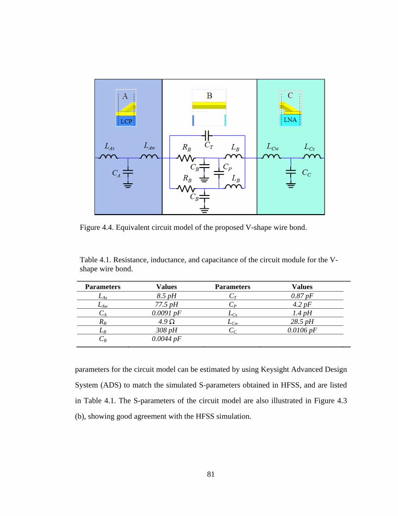
81
parameters for the circuit model can be estimated by using Keysight Advanced Design
System (ADS) to match the simulated S-parameters obtained in HFSS, and are listed
in Table 4.1. The S-parameters of the circuit model are also illustrated in Figure 4.3
(b), showing good agreement with the HFSS simulation.
Figure 4.4. Equivalent circuit model of the proposed V-shape wire bond.
Table 4.1. Resistance, inductance, and capacitance of the circuit module for the V-shape wire bond.
Parameters Values Parameters Values LAs 8.5 pH CT 0.87 pF LAw 77.5 pH CP 4.2 pF CA 0.0091 pF LCs 1.4 pH RB 4.9 � LCw 28.5 pH LB 308 pH CC 0.0106 pF CB 0.0044 pF

82
4.4 Multi-Chip Module
4.4.1 Single-LNA Module
The study of a MCM begins with a single-LNA module, which consists of one
ALP283 LNA chip, two MS line feeds, a pair of CBCPW probe pads, and bias circuit,
as shown in Figure 4.5 (a). The LNA chip is embedded in a pocket in the top LCP
layer, and integrated with MS lines using V-shape wire bonds. The practical wire
bonds have a length (L) varying from 210 to 235 μm, a flared width (W) varying from
133 to 160 μm, and a height (H) varying from 15 to 35 μm. Based on the tolerance
analysis, these variations do not change the insertion loss of the V-shape wire bond
significantly. The net loss of the single-LNA module can be estimated by combining
the insertion losses of the individual components, including probe pads, V-shape wire
bonds, and two 3mm long MS lines, and are illustrated in Figure 4.5 (b). It can be seen
that the simulated net loss of the single-LNA module is less than 3.8 dB at W-band.
Next, the net gain of the single-LNA module can be estimated by subtracting its net
loss from the LNA’s on-chip measured gain. The estimated net gain is higher than 27
dB from 80 to 100 GHz, as depicted in Fig. 5 (c).
Throughout this measurement, the system set-up and calibration method
aforementioned in Section 3.2 were utilized to characterize the single-LNA model as
well as the following double-LNA module. The measured gain of the single-LNA
module is illustrated in Fig. 4.5 (c). A high gain of 26.5-29.5 dB is demonstrated from
80 to 100 GHz, showing good agreement with the estimated gain. The discrepancy
between the measured and calculated gain curves may be attributed to the fabrication
and integration tolerance as well as the chip-to-chip gain variation.

83
(a)
(b) (c)
Figure 4.5. (a) Configuration of the single-LNA module, (b) simulated net loss of the single-LNA module and double-LNA module, and (c) measured and calculated net gain of the single-LNA module.
4.4.2 Double-LNA Module
After successfully integrating and characterizing the single-LNA module, a
MCM with two ALP283 LNA chips was investigated, as illustrated in Figure 4.6.
Differing from the single-LNA module, substrate integrated waveguides (SIWs) are

84
designed and distributed between LNAs, and via barriers are distributed in the inactive
region of the LCP carrier to minimize the undesired substrate modes in the carrier
substrate. The diameter and pitch of the vias are 250 and 300 μm, respectively. The
width of the SIW is 1.7 mm, and the corresponding cut-off frequency is approximately
58 GHz. Thereby, the SIWs can only support TE10 mode at W-band. The length of the
three SIWs is 6, 8, and 6 mm, respectively. The SIW-to-MS transition presented in
Section 3.2 is utilized to connect the SIWs with the MS lines, whose insertion loss is
less than 0.7 dB from 70 GHz to 110 GHz. To eliminate the low-frequency
oscillations, bypass capacitors are employed as high pass filters in the bottom circuit
layer, as illustrated in Figure 4.6. As can be found in Figure 4.5 (b), the net loss of the
Figure 4.6. Packaged double-LNA module and 3-D printed housing.

85
passive components in the double-LNA module, including SIWs, MS lines, SIW-to-
MS transitions, CBCPW probe pads, and V-shape wire bonds, is less than 11.3 dB
from 70 to 100 GHz. Thus, the net gain of the module can be calculated by subtracting
its net loss (Figure 4.5 (b)) from two times of the on-chip gain of the LNA (Figure 4.1
(b)). Figure 4.7 (b) illustrates the estimated and measured net gain of the proposed
module. The measured gain is higher than 45 dB from 78 to 100 GHz, and higher than
50 dB from 81 to 92 GHz, showing good agreement with the calculated data. The
discrepancy can be attributed to the aforementioned reasons for the single-LNA
module. The unwrapped phase of the double-LNA module is illustrated in Figure 4.6
(c), showing linearity at the working frequencies.
In wireless communication systems, NF is an important factor to describe
noise performance, and determines the receiver’s sensitivity. The NF of cascaded
devices can be expressed as follows [79]:
��� � ��� ���� �
����� �
������ �
���� � �����
where ��� and � (n is an integer) are the noise figure and gain of the cascaded nth
element, respectively. Thus, the module’s NF can be estimated by plugging the on-
chip measured gain of a single LNA (Figure 4.1 (b)), the simulated insertion losses of
the passive components, and the LNA’s NF in NG’s datasheet [73] into Equation (4.9).
Figure 4.7 (c) illustrates the calculated and measured NFs of the proposed double-
LNA module. The measured NF is characterized by using Y-factor method [79]. A W-
band noise diode, QNS-FB15LW from Quinstar Inc., was integrated in front of the
module as an excess noise ratio (ENR) source. By turning the noise diode on and off,
Y-factor can be measured, and the NF of the module can be extracted. The measured

86
NF of the proposed double-LNA module is less than 6 dB from 77 to 97 GHz, which
is in good agreement with the calculated data. The small discrepancy can be attributed
to the integration tolerance and the chip-to-chip NF variation. NG’s datasheet [73]
only provides the NF from 75 to 100 GHz. Thus, the measured NF is given in the
same spectrum.
(a) (b)
(c)
Figure 4.7. Measured and calculated (a) net gain, (b) unwrapped phase, and (c) noise figure of the double-LNA module.

87
4.5 Packaging Technologies
Traditional mmW packaging utilizes metals [25] or ceramics [63], both of
which are expensive, and have their own independent limitations. The metallic
packaging is typically bulky and heavy, and ceramics require detrimentally high
lamination temperature. As an alternative, inexpensive plastic packaging has gained
great interest recently. References [70], [72], and [74] reported semi-hermetic organic
packaging by laminating multilayer LCP substrates. However, these LCP packages
cannot provide metallic cavities to isolate the MMICs from electromagnetic
interference (EMI) in the high gain MCMs at high frequencies, i.e., W-band.
I proposed using 3D-printed resin housing coated with gold to encapsulate the
LNAs, as illustrated in Figure 4.6. The length of the housing cavity is 6 mm, and the
width and depth are 3 mm. The proposed housing was adhered on the top grounds of
the SIWs and inactive regions to cover each LNA using silver epoxy, and provides
light weight and low cost to module packaging and electromagnetic isolation, quasi-
hermetization, and mechanical buffering to the LNAs. The measured gain, phase, and
NF of the proposed double-LNA module with housing are also illustrated in Figure 4.7
(a), (b), and (c), respectively. It can be found that the proposed housing introduces
little degradation to the performance of the double-LNA module.
4.6 Summary
In this chapter, I presented the MCM integration and packaging technologies,
i.e., multilayer carrier, laser-drilled cavities, and V-shape wire bonding, and a 50dB
gain double-LNA module at W-band using a four-circuit layer LCP substrate as a
MMIC carrier. The utilized LCP carrier consists of four circuit layers, i.e., the top two
for the RF components and the bottom two for the bias circuits. To reduce the wire

88
bond’s inductance, the LNA chip is embedded into a laser-drilled pocket in the top
LCP layer. To minimize the mode mismatch between the MS lines on the LCP
substrate and LNAs as well as further reduce the wire bond’s inductance, V-shape
wire bonds are designed to integrate the LNAs with MS lines. The single-LNA
module achieves a high gain of more than 26.5 dB from 80 to 100 GHz. In the MCM,
SIWs and via barriers are designed to eliminate the undesired substrate modes in
carrier substrates, and 3D-printed gold-coated housings are designed to encapsulate
the LNAs and isolate them in free space. An impressive gain of 45-52 dB and a low
NF of less than 6 dB were demonstrated for the double-LNA module from 80 to 100
GHz. The proposed module also achieves linear phase at the working frequencies.

89
SIW FILTER AND DIRECTIONAL FILTER AT W-BAND
The most obvious application of a filter is to reject the unwanted signal
frequencies while permitting good transmission of the desired frequencies [80].
According to their spectral response, filters can be classified into different categories,
i.e., low-pass, high-pass, band-pass, and band-reject. Their applications can be found
in virtually any type of microwave or millimeter wave wireless communication, radar,
radiometry, and measurement systems. In the general sense, PCBs serve as the
foundation for virtually all these systems. In the printed circuits of these systems,
compact filters can be designed on various transmission lines, i.e., MS lines, CPWs,
and SIWs. Traditionally, most filters are two-port structures, in which the desired
frequencies pass through, and the undesired ones are reflected. However, the strong
reflection may introduce many problems, i.e., noise, substrate modes, and oscillation,
in the compact mmW systems, particularly for high-gain active applications. To
mitigate the reflection, a four-port directional filter has been developed, which can
pass the desired frequencies to one port and drop the undesired spectra to another port
with low reflection and good isolation at the other two ports. Directional filters have
found many applications in the high-gain systems and frequency division multiplexing
of wireless communications at microwave frequencies.
In this chapter, I present a SIW-based two-port bandpass filter and a MS-based
four-port bandpass directional filter in multilayer LCP substrates, which can be
applied to many wireless applications at W-band. As presented in Section 3.1, MS
Chapter 5

90
lines and SIWs are the two main transmission lines for the proposed front-end
receiving module. Thus, the filter design is based on these two components. This
chapter is organized as follows. In Section 5.1, I will discuss the detailed challenges
for the printed filters on LCP substrates as well as other substrates at W-band. Then,
the SIW-based filter and MS-based directional filter will be presented in Section 5.2
and Section 5.3, respectively. This is followed with a summary and conclusion.
5.1 Challenges for W-band Filters
In Section 1.2, I have discussed the challenges in materials, fabrication,
electromagnetic interference, and measurement for W-band frequencies. In this section,
I discuss the detailed challenges for the W-band filters in multilayer LCP substrates
fabricated using commercial large-panel PCB technologies. Under the commercial
fabrication standards, the minimum resolution of circuit patterns is 50 μm, and the
diameter and pitch of the micro vias are 250 μm and 300 μm, respectively. The via’s
annular ring is suggested to be 125 μm larger than its hole [9].
Typically, the two-port filters can be designed on MS lines, CPWs, and SIWs.
Among these three transmission lines, MS lines and SIWs are of great preference in
multilayer printed circuits due to their good electrical shielding. The filters based on
MS lines [80] and SIWs [44] have been thoroughly investigated at microwave
frequencies. However, their applications for W-band frequencies are limited by
commercial fabrication resolution. On one hand, the traditional MS line based filters
are designed using cascaded half-wavelength impedance steps [80], or half-
wavelength and/or quarter-wavelength MS lines with capacitive coupling [80]. The
former require narrow line width to achieve high impedance, and the latter need tiny
gaps to obtain sufficient coupling at W-band, both of which, however, cannot be

91
fabricated using the commercial large-panel circuit printing technologies. The
interdigital filters with vias [80] can be designed with gaps wider than 50 μm between
the adjacent MS lines. However, the electrically ‘large’ ring of the vias may change
the resonant frequency and short-circuit the neighboring lines. On the other hand, the
SIW-based filters can be designed using quarter-wavelength inductive coupling or
cascaded cavities with irises [44]. The inductive posts and irises are typically defined
using vias, which are practical at low frequencies. However, the diameter and pitch of
the vias becomes electrically ‘large’ at W-band, which may potentially increase the
SIW’s leakage, introduce difficulties to precisely define cavities, and reduce the
quality factor of the cavities. Also, the registration tolerance of the vias for the
inductive posts and irises may change the center frequency of SIW filters. Compared
to the MS-based filters, the SIW-based filters are more robust and practical to the
commercial large-panel fabrication technologies at high frequencies. To this end, the
SIW-based filters are investigated in this dissertation.
A directional filter is a four-port structure, consisting of one travelling-wave
resonator or two standing-wave resonators, terminating lines, and tiny gaps between
them to obtain sufficient coupling. It can be designed on MS lines, SIWs, and SLs in
printed circuits. The most critical parts of a directional filter are the resonator and the
coupling gaps between the resonator and terminating lines. SIWs are not preferable for
directional filters due to the fact that their width is too electrically ‘large’ to achieve
compact resonators. The SL-based and MS-based direction filters suffer from the low
coupling efficiency of the gaps, which aggravated as the frequency increases. As the
frequency increases to W-band, the traditional directional filters based on MS lines and
SLs encounter significant insertion loss and reflection, which is mainly limited by the

92
commercial fabrication standards. To the best of my knowledge, no directional filters
have been reported at W-band so far. New topologies have to be invented for the
directional filters at W-band.
5.2 SIW Filter at 94 GHZ
Recently, substrate integrated waveguides have been investigated to substitute
for traditional rectangular waveguides in printed circuits at microwave/mmW
frequencies, due to their low profile, high density, light weight, and simple packaging.
A SIW is a waveguide-like structure fabricated in a dielectric substrate by using two
rows of metal vias to connect the top and bottom parallel conductor layers. It preserves
most of the advantages of conventional air-filled RWGs, including high quality factor,
high power-handling capability, and good electrical shielding. Originating from the
planar H-plane RWG filters, SIW filters have gained great interest in the last decade.
The SIW filters are superior over the traditional waveguide filters and planar
transmission line filters due to the aforementioned benefits. According to the coupling
topologies, SIW filters can be classified into four categories: inductive post, iris
windows, circular cavities, and rectangular cavities with cross-coupling [44]. Most
SIW filters reported so far are designed below 60 GHz [81]-[84], and fabricated on
small panels.
The ultimate application of SIW filters and other passive components is in
large-scale printed circuits, which becomes dominant in the circuit market due to their
low unit cost and high manufacturing speed. However, it has to sacrifice the resolution
of the minimum features in the fabrication. According to the commercial standards [9],
the vias’ pads should be 125 μm larger than their holes, and the diameter and pitch of
vias are suggested to be at least 250 μm in the multilayer circuits of the proposed

93
receiving module, which is large in terms of wavelength at W-band. These commercial
standards introduce many detrimental impacts to the design and measurement of SIW
filters at high frequencies, as discussed in Section 5.1.
In this section, I present a second-ordered SIW filter, and demonstrate its
application on a 100μm thick 12×18 inch LCP panel using the state-of-the-art large-
panel circuit print technologies. The SIW filter achieves an insertion loss of 1.5 dB at
94 GHz and a passband of 8% centered at 94 GHz.
5.2.1 SIW Filter Design
Differing from traditional RGWs, SIWs can only support TEm0 modes due to
their electrically ‘small’ substrate thickness in terms of wavelength. For the structure
illustrated in Figure 5.1, the fundamental mode of the SIW cavities is TE110 mode. The
initial cavity dimensions can be determined by setting the resonant frequency of the
TE110 mode equal to the center frequency of the desired passband, as described by the
following formula:
�� � ������ �� �� ������ �� � �� �� ������ ��� ���� where �� is the dielectric constant, � and � are the SIW cavity’s width and length, �
is the diameter of the vias, and � is the pitch size between two contiguous vias.
In this section, simple topologies and low orders are employed for the SIW
filter, which are robust in my view with respect to the commercial state-of-the-art PCB
manufacturing, to investigate application possibility of SIW filters in large scale
printed circuits at W-band. The diameter and center-to-center pitch of vias are d = 250
and p = 300 μm, respectively, which could be utilized in a multilayer substrate with a

94
thickness of 200 μm. The filter is second-ordered using one iris window as a coupling
element and two MS lines as feeds. The cavities and windows are carefully defined
using laser-drilled vias. Ansys HFSS was employed to design a full-wave model for
the proposed filter, as illustrated in Figure 5.1, and tune the cavity dimensions to
optimize the insertion loss and center frequency of the filter. To attain an impedance
of 50 �, the width of the MS lines is chosen as 240 μm, and the length and width of
the two identical cavities are 2 and 0.9 mm, respectively. The widths of the feed
window, W1, and iris window, W2, are 0.96 and 0.8 mm, respectively. Figure 5.2 (b)
illustrates the simulated S-parameters of the second-ordered SIW filter. It can be found
that the 3dB passband is from 90.8 to 98.5 GHz, and the insertion loss is 1.5 dB at 94
GHz. The stopband attenuation is 36 and 11 dB at 70 and 110 GHz, respectively. The
out-of-band attenuation could be improved by cascading additional cavities.
Figure 5.1. Configuration of the second-ordered SIW filter fed by MS lines.
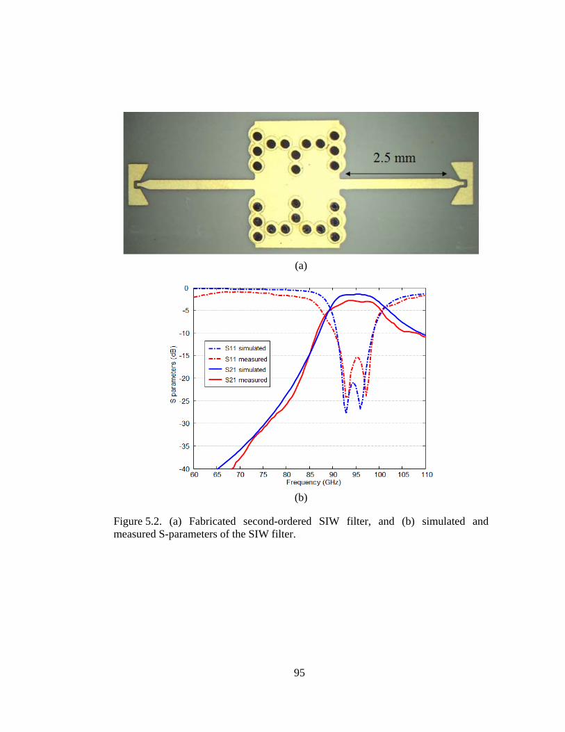
95
(a)
(b)
Figure 5.2. (a) Fabricated second-ordered SIW filter, and (b) simulated and measured S-parameters of the SIW filter.

96
5.2.2 Measurement
The fabricated SIW filter is illustrated in Figure 5.2 (a). It comprises two
identical cavities constructed with only twenty four vias and two MS lines terminated
with a pair of low-loss CBCPW probe pads. The design and measurement of the probe
pads have been presented in Section 3.3.2. The measurement set-up and calibration
method discussed in Section 3.2 were employed for the characterization of this filter.
Figure 5.2 (b) illustrates the measured S-parameters. It can be seen that the measured
insertion loss is 2.6 dB at 94 GHz, including the two probe pads’ loss, and the 3dB
bandwidth is from 90.8 to 98.5 GHz. As can be found in Figure 3.8 (c), the averaged
insertion loss of a pair of CBCPW probe pads is approximately 0.8 dB at 94 GHz.
Thus, the true loss of the fabricated filter is 1.8 dB, showing little discrepancy with the
simulated loss. The out-of-band rejection is 36 dB at 70 GHz and 11 dB at 110 GHz,
respectively. The simulated and measured S-parameters are in good agreement, which
demonstrates that the SIW filter can be utilized in large-panel printed circuits.
5.3 Directional Filters at 95 GHZ
Directional filters (DFs) have gained tremendous interest in the application of
frequency division multiplexing (FDM) in wireless communication systems. They can
act either as channel combiners or channel separators. Superior over the other
multiplexers, the DFs address miniaturization and low reflection. Various DFs have
been devised since the 1960s, however, a limited number of them have found practical
applications. Figure 5.3 illustrates the most useful types of the reported DFs. Ideally, a
broadband signal fed into Port 1 of the DFs will be isolated at Port 4, the desired
spectrum will be dropped to Port 3, and the signal at the undesired frequencies will
travel to Port 2, with no reflection at Port 1 [80]. According to this mechanism,

97
directional filters can be classified into three categories: waveguide-based DFs [85],
standing-wave DFs [86]-[90], and travelling-wave DFs [90]-[96]. The waveguide-
based DF comprises two rectangular waveguides and one cylindrical direct-coupled
cavity resonator, as depicted in Figure 5.3 (a). Typically, it is bulky and heavy, and
has a narrow bandwidth of less than 2 percent due to the high quality factor of the
waveguide structures [80] [85]. Figures 5.3 (b) and (c) illustrate two types of standing-
(a) (b)
(c) (d)
Figure 5.3. Traditional directional filters: (a) waveguide-based, (b) standing-wave I, (c) standing-wave II, and (d) travelling-wave.
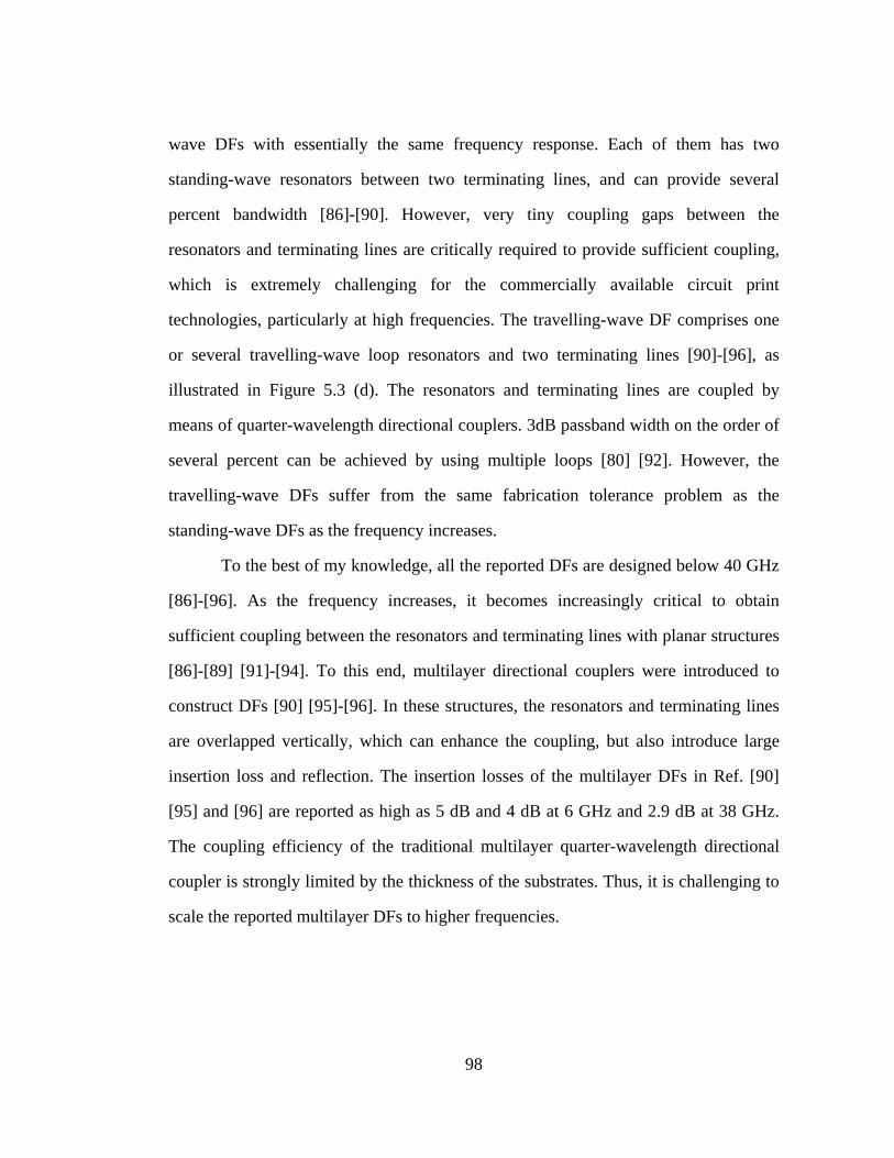
98
wave DFs with essentially the same frequency response. Each of them has two
standing-wave resonators between two terminating lines, and can provide several
percent bandwidth [86]-[90]. However, very tiny coupling gaps between the
resonators and terminating lines are critically required to provide sufficient coupling,
which is extremely challenging for the commercially available circuit print
technologies, particularly at high frequencies. The travelling-wave DF comprises one
or several travelling-wave loop resonators and two terminating lines [90]-[96], as
illustrated in Figure 5.3 (d). The resonators and terminating lines are coupled by
means of quarter-wavelength directional couplers. 3dB passband width on the order of
several percent can be achieved by using multiple loops [80] [92]. However, the
travelling-wave DFs suffer from the same fabrication tolerance problem as the
standing-wave DFs as the frequency increases.
To the best of my knowledge, all the reported DFs are designed below 40 GHz
[86]-[96]. As the frequency increases, it becomes increasingly critical to obtain
sufficient coupling between the resonators and terminating lines with planar structures
[86]-[89] [91]-[94]. To this end, multilayer directional couplers were introduced to
construct DFs [90] [95]-[96]. In these structures, the resonators and terminating lines
are overlapped vertically, which can enhance the coupling, but also introduce large
insertion loss and reflection. The insertion losses of the multilayer DFs in Ref. [90]
[95] and [96] are reported as high as 5 dB and 4 dB at 6 GHz and 2.9 dB at 38 GHz.
The coupling efficiency of the traditional multilayer quarter-wavelength directional
coupler is strongly limited by the thickness of the substrates. Thus, it is challenging to
scale the reported multilayer DFs to higher frequencies.

99
In this section, I present a new type of travelling-wave DF fabricated using
multilayer liquid crystal polymer (LCP) substrates at 95 GHz. It comprises two dual-
slot directional couplers and one two-wavelength long loop resonator. The proposed
filter is superior to the traditional symmetric travelling-wave DF by using asymmetric
loop phase topology and the developed dual-slot directional couplers. To improve the
directivity and reduce the insertion loss, cascaded DFs were also designed and
characterized. The proposed DFs have no critically sized features, and were fabricated
on 12×18 inch LCP panels by using commercial large-scale circuit print technologies.
This section is organized as follows. Section 5.3.1 will discuss the proposed dual-slot
directional coupler. Then, the design of the single-loop and cascaded double-loop DFs
in LCP multilayer substrates will be depicted in Section 5.3.2. Section 5.3.3 will
present the hybrid substrates, measurement setup, and measured results of the
proposed DFs.
5.3.1 Directional Coupler Design
The traditional travelling-wave DF comprises loop resonators and quarter-
wavelength directional couplers [90]-[92] [94]-[96], as illustrated in Figure 5.3 (d).
The couplers can be designed either using planar parallel lines with very narrow
coupling gaps or vertically parallel lines in multilayer thin substrates. Reference [97]
reported a directional coupler based on double-sided MS lines coupled through a slot
with a length of quarter wavelength in the shared ground in multilayer substrates.
However, these reported structures are not suitable for high-frequency applications
due to the aforementioned problems of the reflection and coupling efficiency.
Inspired by the multi-hole rectangular waveguide coupler [11], we designed a
new type of dual-slot MS line based directional coupler in three-layer LCP substrates.

100
The proposed directional coupler comprises two parallel MS lines on the top and
bottom layers, respectively, a shared ground in the inner layer, and two rectangular
slots distributed in the ground with a pitch of a quarter wavelength of the MS lines.
5.3.1.1 Slot coupling of the vertically overlapped MS lines
To understand how the proposed directional coupler operates, the coupling
mechanism of two vertically overlapped MS lines is first investigated. Its
configuration and electric fields along the propagation direction of the guided wave
are illustrated in Figure 5.4 (a). According to Ref. [11], for a signal sent into Port 1, it
can excite an even mode to Port 4 and an odd mode to Port 3. For the even mode, the
electric field is evenly symmetric according to the center line, thus no current flows
between the two MS lines. For the odd mode, the field shows an odd symmetry, and a
voltage null exists between the two strip conductors. Thus, these two modes propagate
in opposite directions. The equivalent circuit models of these two modes are also
illustrated in Figure 5.4 (a). C12 represents the coupling capacitance between the top
and bottom MS lines, and C11 and C22 represent the capacitances of these two lines to
the shared ground. Due to the small coupling slot, the capacitance (C12) is not
significant, and, thereby, the even and odd modes have similar amplitude.
Ansys HFSS was employed to design and simulate the full-wave models of the
vertically coupled MS lines and the following devices. As illustrated in Figure 5.4 (a),
the bond-ply is a 50μm thick LCP, and the top and bottom LCP core layers are 100
and 50 μm, respectively. The dielectric constant and loss tangent of LCP are 3.2 and
0.0045 at 95 GHz, respectively, as reported in Ref. [8]. The top MS line has a length
of 5 mm and a width of 0.24 mm, providing an impedance of 50 � for probing. A
narrower width of 0.16 mm is chosen for the bottom MS lines to suppress the

101
dispersion of the loop resonator [8] [71] in the DFs. As can be seen in Figure 5.4 (a),
���and ��� represent the odd mode and even mode, respectively, due to the same
propagation directions. Tolerance analysis of the substrate thickness and slot size is
illustrated in Figure 5.4 (b) and (c). The total thickness of the bond-ply and bottom
(a)
(b) (c)
Figure 5.4. (a) Configuration, electric fields, and equivalent circuit models of the slot-coupled vertically overlapped MS lines, and simulated S-parameters of the slot-coupled MS lines with (b) different LCP thickness and (c) slot size.

102
LCP is denoted as ��. As can be seen in Figure 5.4 (b), using a thin substrate can
enhance the coupling efficiency. At �� � �� ��, the simulated � and �� are 1.8 dB
higher than their counterparts at �� � ��� ��. However, the MS lines on a 50μm
thick LCP substrate have significant propagation loss [8], which is not suitable for
practical applications. Increasing the size of the coupling slot can also enhance the
coupling efficiency, however, significantly increasing the reflection, as illustrated in
Figure 5.4 (c). It should be noted that a large slot introduces large discrepancy
between the even mode and odd mode, which can be explained by the equivalent
circuit models in Figure 5.4 (a). The odd mode is controlled by C11, C22, and C12,
while the even mode is determined by C11 and C22. Enlarging the slot can increase C12,
thus enhancing the odd mode faster than the even mode. When the slot width, �,
equals a quarter wavelength, the traditional slot-coupled directional coupler reported
in Ref. [97] can be achieved, however, whose reflection is significant at W-band.
Based on the aforementioned analysis, to compensate for MS line’s loss, reflection,
and coupling efficiency, �� is chosen as 100 μm, and the width, �, and length, ��, of
the slot are 0.12 and 0.5 mm, respectively. The simulated magnitude of the even mode,
�� , and odd mode, � , is -13.6 and -12.9 dB at 95 GHz, respectively, and the
reflection, �, is less than -12 dB from 70 to 100 GHz.
5.3.1.2 Dual-slot directional coupler
The configuration and mechanism of the proposed directional coupler are
illustrated in Figure 5.5 (a). It consists of two coupling slots in a shared ground with a
phase delay of 90º and an optimized distance of ps = 3.4 mm along the propagation
direction of the guided wave. Due to the weak coupling of the slots, the two even
modes and two odd modes excited by these two slots have similar amplitude. The two

103
even modes, propagating toward Port 4, are in-phase at the second slot, thus adding
constructively, while the two odd modes, propagating towards Port 3, are 180° out-of-
phase at the first slot, thus providing a high isolation, as depicted in Figure 5.5 (a). The
simulated S-parameters of the dual-slot directional coupler are illustrated in Figures
(a)
(b) (c)
Figure 5.5. (a) Configuration, (b) simulated S11 and S31, and (c) simulated S21 and S41 of the directional coupler in LCP substrates and hybrid substrates.

104
5.5 (b) and (c), showing good directivity. It can been seen that ��� is -7.5 dB, ���is
less than -30 dB, and ���is less than -30 dB at 94 GHz. Due to the high directivity, the
proposed directional coupler can be utilized to design directional filters.
5.3.2 Directional Filter Design
Another key element to construct a travelling-wave DF is the loop resonator.
The traditional DFs utilize loop resonators with a mean circumference of one
wavelength at its center frequency [90]-[96], which is not suitable for high frequencies.
As the frequency increases to W-band, i.e., 95 GHz, the widths of MS lines and
coupling slots become electrically ‘large’ in terms of wavelength. In this case, the one
wavelength loop resonator cannot provide enough space to combine with the proposed
dual-slot directional filter efficiently. Meanwhile, the limited loop length of a one
wavelength loop with ‘large’ line width may increase mutual coupling between the
MS lines in the loop, thus reducing the resonator’s Q-factor. To mitigate this problem,
the mean circumference of the loop resonator is chosen as two wavelengths of the MS
line at 95 GHz. The configuration of the utilized loop resonators is illustrated in Figure
5.6 (a). Its mean length and width are 1.32 mm and 0.71 mm, respectively. The width
of the bottom MS line is 0.16 mm, providing an impedance of 62 � to suppress the
dispersion of the loop resonator. Figure 5.7 illustrates the simulated effective dielectric
constant and propagation loss of the MS lines with a width of 160 μm. It can be seen
that their propagation loss is 0.156 dB/mm at 95 GHz. The simulated unloaded Q-
factor of the loop resonator is 58 at 95 GHz, which can be calculated using the
methods reported in Ref. [8] and [71]. Then, the corresponding averaged attenuation
of the loop resonator can be calculated as 0.226 dB/mm, including the radiation loss
and propagation loss of the loop line [71]. The averaged radiation loss can be obtained

105
by subtracting the propagation loss illustrated in Figure 5.7 (b) from the total loss. The
estimated radiation loss is approximately 0.065 dB/mm at 95 GHz, which is not
significant with respect to the total loss.
(a)
(b) (c)
Figure 5.6. (a) Configuration of the single-loop DFs with symmetric and asymmetric loop topologies in multilayer LCP substrates, and simulated S-parameters of the (b) symmetric and (c) asymmetric DFs with ps = 0.35 mm.

106
5.3.2.1 Single-loop directional filter
5.3.2.1.1 Symmetric loop
I first investigated a DF with a symmetric loop, which is typically utilized for
the traditional travelling-wave DFs [90]-[96], as illustrated in Figure 5.6 (a).
According to the directional coupler’s mechanism aforementioned in Section 5.3.1, the
signal input to Port 1 will be dropped at Port 3, and isolated at Port 4 at 94 GHz. The
pitch between the two coupling slots, ��, is optimized to 0.35 mm, instead of 0.34 mm,
to achieve a higher directivity for the DF. Figure 5.6 (b) illustrates the simulated S-
parameters of the proposed symmetric DF. The insertion loss of the passband, ���, is -
4.6 dB at Port 3 at 94 GHz, and the 3dB bandwidth is 5.3% centered at 94 GHz. It
should be noted that the through loss, ���, is as high as -9.5 dB, which is limited by
(a) (b)
Figure 5.7. Simulated (a) effective dielectric constant and (b) loss of MS lines with a width of 160 μm on a 100μm LCP substrate and a 50μm LCP substrate laminated with a 66μm AG bond-ply.

107
the coupling efficiency, and can be reduced by cascading directional filters. The
isolation, ���, and reflection, ���, are better than -17 dB at 94 GHz at Port 4 and Port
1, respectively.
However, the symmetric loop reduces the directivity of the DF inherently. As
can be seen in Figure 5.6 (a), the phase between Slot 1 and Slot 2 and between Slot 3
and Slot 4 is approximately 90º, and the phase between Slot 1 and Slot 3 and between
Slot 2 and Slot 4 is 270º. With such a phase distribution, the signals transmitted from
Port 1 to Port 3 in the clockwise and anti-clockwise directions are 180º out of phase,
which actually degrades the directivity.
5.3.2.1.2 Asymmetric loop
To improve the directivity of the DF, I proposed an asymmetric loop topology,
as depicted in Figure 5.6 (a). This asymmetric phase topology is similar to that of the
standing-wave DF [88] in Figure 5.3 (b). The center of the loop is shifted by a factor
of 0.45 mm with respect to the slots. In this case, the phase between Slot 1 and Slot 3
and between Slot 2 and Slot 4 becomes approximately 180º and 360º, respectively.
With such a phase distribution, the signals transmitted from Port 1 to Port 3 in the
clockwise and anti-clockwise directions are constructive, and the counterparts from
Port 1 to Port 2 and from Port 1 to Port 4 are 180º out of phase, thus improving the
directivity of the DFs. The simulated S-parameters of the asymmetric single-loop DFs
are illustrated in Figure 5.6 (c). The 3dB bandwidth of the passband is reduced from
5.3% to 4.9%, the out-of-band rejection is improved more than 5 dB, and the isolation
and reflection are also improved dramatically.

108
5.3.2.2 Double-loop directional filter
Typically, to improve the directivity and the insertion loss, the travelling-wave
DFs may cascade multiple loop resonators [92], as illustrated in Figure 5.3 (d), and the
standing-wave DFs can cascade the identical DFs along the terminating lines [88].
Here, I cascade two identical single-loop DFs in the direction of the terminating lines
with the same topology for the standing-wave DFs, as illustrated in Figure 5.8 (a). The
Port 1 and Port 3 of the second DF connect to the Port 2 and Port 4 of the first DF,
respectively. The ��� and ��� of the first DF will travel to the second DF as the input
signals, and can be depicted by the following formula:
���� � ���
� ��
����� � ���
� ��
where ���� and ���� are the through and isolated signals of the first DF, respectively, �
is the phase delay between two DFs, and ���� and ����� are the input signal to the Port 1
and Port 3 of the second DF, respectively. Due to the symmetry of the proposed DF,
the S-parameters satisfy the following relationships:
���� � ���
� � ���� � ���
�
���� � ���
� .
Both ���� and ����� will be filtered using the same mechanism. Thus, the fundamental
response of the second DF will be the overlapped responses of these two signals:
���� � ���
� ���� � ���
�� ���� � ����
� ���� � ���
� ���� ���
���� � ���
� ���� � ���
�� ���� � ����
� ���� � ���
� ���� ���
���� � ���
� ���� � ���
�� ���� � ����
� ���� � ���
� ���� ���
���� � ���
� ���� � ���
�� ���� � ����
� ���� ���
(5.2)
(5.3)
(5.4)
109
���� and ���� will be fed back to the first DF, part of which will contribute to ���� and
���� and the rest of which will be reflected back to the second DF as the high-order
mutual coupling between the two DFs. As can be found in Figure 5.6 (c), the ���� , ���� ,
(a)
(b) (c)
Figure 5.8. (a) Configuration of the cascaded double-loop DF with asymmetric loops, and simulated S-parameters of the cascaded DF with Pd = (b) 1.9 mm and (c) 2.3 mm.

110
.
(5.5)
and ���� of the single-loop DF are less than -20 dB, -10 dB, and -17 dB at 95 GHz,
respectively. Therefore, it is fair to neglect the high-order mutual coupling and high-
order items, simplifying our analysis. The S-parameters of the cascaded double-loop
travelling-wave DF can be described as follows: 1 2 1 2 1
11 11 11 12 31 141 1 1 1 1 1 2 1 1 1 1 1 211 21 21 11 41 31 41 21 31 41 11
1 1 1 1 211 21 41 31
( ) ( )
2
T j j
j j
j
S S S e S S e S
S S S S S S e S S S S S e
S S S S e
� �
� �
�
� �
� �
�
� � �
� � � � �
� � 2 1 1 1 1
21 21 21 21 41 41( )T jS S S S S S e � �
1 2 1 2 131 31 31 34 11 32
1 1 1 1 1 1 2 1 1 1 1 1 231 21 21 31 41 11 41 21 11 41 31
1 1 1 1 2 1 1 1 231 21 21 31 41 41 31
( ) ( )
T j j
j j
j j
S S S e S S e S
S S S S S S e S S S S S e
S S S S e S S S e
� �
� �
� �
� �
� �
� �
� � �
� � � � �
� � � 2 1 1
41 41 21 412T jS S S S e � �
It is noted that the S-parameters of the cascaded DFs have periodic characteristics,
which are controlled by the phase delay, �, between them. ���� is maximum at � = n�
(n is an integer) and minimum at � = (2n+1)�/2. Limited by the loop dimensions, � =
2� is chosen to reduce the insertion loss, which corresponds to Pd = 1.9 mm. The
simulated S-parameters of the cascaded double-loop DF with Pd = 1.9 mm are
illustrated in Figure 5.8 (b). Superior to the single-loop DFs, the insertion loss, ���, is
improved to 2.6 dB, and the through loss, ���, is reduced to -17 dB at 94 GHz. The
isolation is better than -20 dB at 95 GHz, and the reflection is less than -11 dB at W-
band. Due to the weak disturbance coupling between the two DFs, the 3dB bandwidth
of the passband is broadened to 8%. Tuning the phase delay can also introduce two
transmission zero points to sharp the passband. As the frequency deviates from the
center frequency, the item ���� ���� � ���
� ���� for ���� in Equation (5.5) approaches one.

111
Thus, at � � (2n+1)�/2, two transmission zero points can be introduced to ���� . The
simulated S-parameters of the double-loop DF with Pd = 2.3 mm and � = 5�/2 are
illustrated in Figure 5.8 (c). The passband width is reduced to 4% centered at 94 GHz
with an increased insertion loss of 4.8 dB.
5.3.3 Hybrid Substrates and Measurement
5.3.3.1 Hybrid substrates
To improve the yield for large panel lamination [9], the manufacturer suggests
using 66μm (2.6mil) thick Arlon GenClad (AG) 280 bond-ply [98] as a substitute to
the LCP bond-ply. Consequently, we have to adapt the directional couplers and filters
in the hybrid substrates. The dielectric constant and loss tangent of the AG bond-ply at
95 GHz is approximately 2.82 and 0.005, respectively, which can be calculated using
classic ring resonator method and transmission line method reported in Ref. [71]. As
can be seen in Figure 5.7, using AG bond-ply slightly reduces the effective dielectric
constant and propagation loss of the MS lines. To maintain the same resonant
frequency, the pitch between slots, ps, is increased to 3.7 mm, and the length and
width of the loop are slightly increased to 1.35 mm and 0.745 mm, respectively. The
unloaded Q-factor and the averaged radiation loss of the loop resonator in the hybrid
substrates are similar to their counterparts in LCP substrates. The AG bond-ply
slightly increases the MS line’s impedance from 62 to 67 �, which is preferable to
suppress the dispersion of the loop resonator. The drawback of the hybrid substrates is
the slightly-reduced coupling efficiency of the slot-coupled double-sided MS lines,
which is due to the fact that AG bond-ply with low dielectric constant (2.82) and large
thickness (66 μm) reduces C21 and C22. The simulated S-parameters of the directional

112
couplers in the hybrid substrates are illustrated in Figure 5.5 (b) and (c). The insertion
loss, ���, is -8.2 dB at Port 4, and the isolation, ���, is better than -30 dB at Port 3 at
around 95 GHz. The coupling efficiency is 0.7 dB lower than that in the LCP
substrates at 95 GHz, which may slightly increase the loss of DFs in hybrid substrates.
The HFSS models of the DFs are modified and re-simulated with an AG bond-ply as a
reference for the measured data.
5.3.3.2 Measurement set-up and W-band load
The measurement setup and calibration method discussed in Section 3.2 were
utilized to characterize the MS-to-SIW transition. To probe the DFs, via-less CBCPW
probe pads presented in Section 3.3.2 were utilized to connect the terminating MS
lines. These probe pads achieve low loss and low reflection at W-band.
To characterize the proposed four-port structures, two ports are probed, while
the remaining two ports should be terminated with perfect loads. However, the
commercially available state-of-the-art 50 � resistors can only function up to 50 GHz.
Beyond 50 GHz, these resistors become inductive, and, thus, cannot serve as perfect
loads. To improve the load performance, we attached RF absorbers onto the MS lines
to attenuate the reflection. CBCPW probe pads terminated MS lines were integrated
with 50 � resistors and high-loss RF absorbers to investigate the reflection. The
utilized resistors are S0402AF from State of the Art Inc. [99], and the absorber
material is C-RAM GDSS from Cuming Microwave Corp. [100]. With only the
resistor load, the reflection is as strong as -4 dB at W-band. With a 10mm long RF
absorber, the reflection is less than -14 dB. With both absorber and resistor, the
reflection can be suppressed down to less than -17 dB at W-band.

113
5.3.3.3 Measured S-parameters
The fabricated single-loop and cascaded DFs are illustrated in Figure 5.9. The
material properties utilized in the HFSS simulation and the dimensions of the HFSS
modules and fabricated devices are listed in Table 5.1, revealing a small fabrication
Figure 5.9. Fabricated single-loop and cascaded DFs with RF absorbers.
Table 5.1. Material properties of the substrates and dimensions of the HFSS models and fabricated devices
Parameters HFSS Fabricated Parameters HFSS Fabricated
W1 0.24 mm 0.228 mm �r (LCP) 3.2
W2 0.16 mm 0.15 mm tan� (LCP) 0.0045
Ws 0.12 mm 0.126 mm �r (AG) 2.82
Ls 0.5 mm 0.508 mm tan� (AG) 0.005
Tcopper 17 μm 17±3 μm TAG 66 μm 62-67 μm
114
tolerance. During the measurement, different ports of the DFs were terminated
properly to characterize the corresponding S-parameters. To simplify the load switch
for the two terminated ports, we utilized 10mm long RF absorbers to attenuate the
reflection. The reflection from these two terminated ports is approximately -16 dB at
95 GHz, which will slightly affect the measured S-parameters of the proposed DFs. In
the practical application, both resistors and absorbers may be required to eliminate the
reflection.
5.3.3.3.1 Single-loop DFs
The simulated and measured S-parameters of the asymmetric single-loop DF in
the hybrid substrates are illustrated in Figure 5.10 (a), showing good agreement. It can
be seen that the measured insertion loss of the passband is 5.2 dB at 95 GHz, and the
3dB bandwidth is 4.8% centered at 95 GHz. The isolation is better than -17 dB, and
the reflection is lower than -16 dB at 95 GHz. Limited by the coupling efficiency of
the directional coupler, the through signal, S21, is approximately -9 dB at 95 GHz. In
this case, the through signal can be fed into another DF to reduce the through loss. The
measured out-of-band rejection of the passband is slight higher than the simulated
result, which may be attributed to the reflection from the terminated ports attached
with RF absorbers.
5.3.3.3.2 Cascaded double-loop DFs
The simulated and measured S-parameters of the cascaded DFs in the hybrid
substrates are illustrated in Figures 5.10 (b) and (c). By cascading two DFs, the
insertion loss (S31), isolation (S41), and through loss (S21) can be improved significantly
with a cost of slightly increased bandwidth and reflection. At Pd = 1.9 mm, the
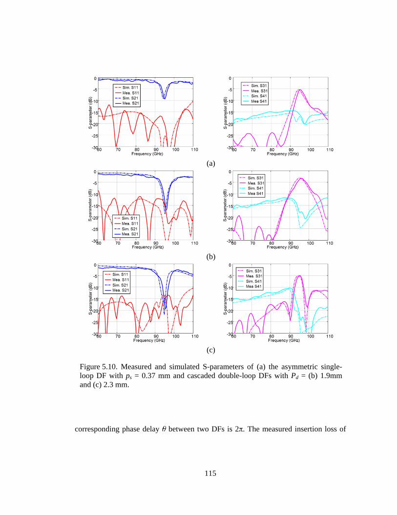
115
corresponding phase delay � between two DFs is 2�. The measured insertion loss of
(a)
(b)
(c)
Figure 5.10. Measured and simulated S-parameters of (a) the asymmetric single-loop DF with ps = 0.37 mm and cascaded double-loop DFs with Pd = (b) 1.9mm and (c) 2.3 mm.

116
the passband is 3.16 dB at 96 GHz, the 3dB passband width is increased to 7.8%
centered at 96 GHz, and the through signal is reduced to -18 dB at the center
frequency. At Pd = 2.3 mm, the corresponding phase delay � between two DFs
becomes 5�/2. The measured insertion loss is increased to 5.4 dB at 95.5 GHz due to
the destructive phase delay between the DFs. Two transmission zero points can be
introduced to achieve a narrow bandwidth of 4% centered at 95.5 GHz. The measured
reflection ��� and isolation ��� of these two cascaded double-loop DFs are below -12
and -10 dB, respectively.
The center frequency of the measured data is slightly higher than that of the
simulated ones, which can be attributed to the over etching. The over etching slightly
reduces the loop length as well as the width of the MS lines, which slightly reduces the
effective dielectric constant. The insertion losses of the DFs in the hybrid substrates
Table 5.2. Insertion loss, bandwidth, and out-of-band rejection of the directional filters.
Sub. Config. Pd (mm) loss (dB) BW Rejection (dB) LCP S. Sym. 4.6 5.8% -25(L)/-11(H)
Hybrid S. Sym. 5.3 6% -27(L)/-12(H) LCP S. Asym. 4.6 4.9% -30(L)/-14(H)
Hybrid S. Asym. 5.2 4.8% -30(L)/-16(H) LCP D. Asym. 1.9 2.5 8% -27(L)/-23(H)
Hybrid D. Asym. 1.9 3.16 7.8% -40(L)/-26(H) LCP D. Asym. 2.3 4.8 4.2% -20(L)/-11(H)
Hybrid D. Asym. 2.3 5.4 4.0% -20(L)/-12(H)
Sub. and Config. denote the substrates and loop configuration, respectively. BW and Rejection denote the 3dB bandwidth and out-of-band rejection of the passband,
respectively. (L) and (H) denote at low and high frequencies, respectively. S. and D. denote single-loop and double-loop, respectively.

117
are approximately 0.7 dB lower than their counterparts in LCP substrates, which is due
to the AG bond-ply with low dielectric constant and large thickness. Cascading two
single-loop DFs can reduce the insertion loss by a factor of 2 dB. The insertion loss,
bandwidth, and out-of-band rejection of the single-loop and double-loop DFs in the
LCP substrates and hybrid substrates are listed in Table 5.2.
5.4 Summary
In this chapter, I first discussed the detailed challenges for the design of filters
and directional filters using the commercial state-of-the-art circuit print technologies
in Section 5.1. Then, a second-ordered SIW-based filter 94 GHz was presented in
Section 5.2, consisting of two cascaded cavities and an iris window. A passband of 8%
centered at 94 GHz and a low loss of 1.5 dB at 94 GHz were demonstrated for the
proposed filter. This effort demonstrates the application possibility of the SIW filters
in multilayer LCP substrates at W-band using commercial PCB technologies. In
Section 5.3, slot-coupled travelling-wave DFs in multilayer LCP and hybrid substrates
were presented. The proposed single-loop DF consists of two dual-slot quarter-
wavelength directional couplers and one loop resonator with a circumference of two
wavelengths at 95 GHz. To improve the directivity, asymmetric loop is carefully
designed. The passband insertion loss and 3dB bandwidth of the single-loop DF in
LCP substrates are approximately 4.6 dB at 94 GHz and 4.9% centered at 94 GHz,
respectively. To further improve the directivity and reduce the insertion loss, two DFs
can be cascaded in series. An insertion loss of 2.6 dB can be achieved for the cascaded
DFs in LCP substrates. Limited by the practical applications, AG bond-ply is utilized
to substitute the LCP bond-ply, slightly reducing the coupling efficiency of the coupler
and increasing the insertion loss of the DFs. The simulated and measured insertion

118
loss of the single-loop and double-loop DFs in the hybrid substrates is increased to 5.4
dB and 3.1 dB at 95 GHz, respectively. This is the first time the DFs are designed and
demonstrated at W-band.

119
CONCLUSION AND FUTURE WORK
In this chapter, I first summarize my work presented in this dissertation and
emphasize the major accomplishments. Then, my following work on the fully-
packaged front-end receiving modules and their applications in wireless systems at W-
band are discussed.
6.1 Conclusion
In this dissertation, I have presented the individual components of a W-band
front-end receiving module based on multilayer liquid crystal polymer substrates,
which can be potentially utilized in a variety of wireless systems, such as wireless
communication, radar, and radiometry. The advantages and benefits of the proposed
module are summarized as follows.
� The passive RF components of the proposed module address low dielectric loss
at W-band due to the low loss tangent and low dielectric constant of the LCP
substrates. Additionally, LCP can provide low cost, light weight, and low
water absorption for the module.
� The developed multilayer circuits achieve small size, light weight, high density
for assembly, low interconnection loss, layer-to-layer isolation, and multi-
function capability.
� MCM technologies enable the proposed module to obtain high net gain and
low noise figure, which are virtually preferable in all wireless receivers.
Chapter 6

120
� The proposed module is fabricated on 12×18 inch LCP panels using the
commercial state-of-the-art large-panel circuit print technologies to reduce the
unit cost and manufacturing cycle as well as enable large-volume production.
The proposed receiving module comprises antennas, various transmission lines and
their transitions, LNAs and their integration circuits, and filters. All these components
except filters can provide an ultra-wide band covering most of the frequencies at W-
band, which can satisfy the bandwidth requirement of the gigabyte data rate wireless
communication. For the narrowband applications, the designed filters can be utilized
to efficiently pick out the spectra of interest with low insertion loss and high out-of-
band attenuation. The developed components can also be utilized for other
applications, such as transmitters and transceivers, whose novelties were presented in
the previous chapters separately:
� In Chapter 1, I first discussed W-band frequencies and the challenges at W-
band. Then, I presented three important wireless applications, namely, wireless
communication, radar, and radiometry, which can use a common front-end
receiving module.
� In Chapter 2, a MS-fed high gain linearly tapered antipodal slot antenna on a
100μm thick LCP substrate was presented. By using an MS-to-APSL balun,
the proposed antenna achieves an ultra-wide bandwidth from 47 to 110 GHz.
An optically-addressed antenna far field measurement system based on optical
upconversion was developed and constructed to characterize the antenna at
high frequencies. A high gain of 17±0.5 dBi, narrow beamwidth, low side
lobes, and low cross-polarization were demonstrated for the proposed antenna
at E- and W-bands.

121
� In Chapter 3, I presented a CBCPW-to-stripline vertical transition, a MS line-
to-SIW transition, a SIW-to-rectangular waveguide transition, and a MS-to-
CPW transition at W-band, all of which can be utilized in the multilayer LCP
based front-end receiving module. The proposed transitions achieve low
insertion loss, low reflection, and ultra-wide bandwidth. Different transmission
lines and the corresponding transitions can be utilized for different applications.
� In Chapter 4, the integration and packaging technologies for high-gain multi-
chip module at W-band were presented. By using these technologies, a double-
LNA module was developed in multilayer LCP substrates, achieving high
density, light weight, low interconnection loss, and perfect EMC at W-band. A
high gain of 46-50 dB, a low noise figure of less than 6 dB, and linear phase
were demonstrated for the proposed double-LNA module from 80 to 100 GHz.
� In Chapter 5, I presented a SIW-based filter and a MS-based directional filter
at 95 GHz. The former is comprised of only twenty four micro vias, and
demonstrates the manufacturing possibility of W-band SIW filters using the
commercial large-panel PCB fabrication technologies. The latter addresses low
reflection and high directivity, and can be utilized for frequency division
multiplexing. This is the first time that directional filters are reported at W-
band. Both filters achieve low insertion loss and high out-of-band rejection at
W-band.
Assembling these components will enable the realization of a high density, high gain,
low noise figure, light weight, and low cost front-end receiving module, as illustrated
in Figure 6.1. To achieve frequency division multiplexing, directional filters can be
integrated into this receiving module. For high-power applications, the last LNA can

122
Figure 6.1. Configuration of a multilayer LCP-based ultra-wideband front-end module.
be substituted with a power amplifier. For a more general application, the linearly
tapered antipodal slot antenna can be replaced by a standard rectangular horn antenna
integrated with the SIW-to-waveguide transition depicted in Section 3.4. The output of
the proposed module can be either a rectangular waveguide or CPW by using the
transitions presented in Chapter 3. The former is suitable for the general applications,
and the latter can be utilized in EO systems.
6.2 Future Work
Future research should focus on additional applications of the W-band front-
end receiving modules in wireless communication, radar, and radiometry systems. For

123
instance, the directional filters can be migrated to other frequencies at W-band, and
cascaded in series to separate the frequencies into different channels in wireless
communication systems. The integration of duplexers and switches on LCP substrates
may also be of great interest. The former is typically utilized for the monostatic radars,
and the latter can be employed for the phased array antenna in radar and
communication systems.
At the University of Delaware, an optically-addressed radiometer, passive
mmW imager, has been developed at 77 GHz using optical upconversion [2], whose
configuration is shown in Figure 6.2. Unlike a focal plane array, a distributed aperture
[21] configuration is utilized in this imager to eliminate the need for mmW lens and
expensive detection electronics for each pixel. The phase and amplitude of the mmW
signals are captured by the antennas distributed in a flat or conformal array. These
signals are then up-converted onto a telecommunication laser carrier, generating two
optical sidebands, and routed via light weight fiber optic waveguides to an optical
processor. This approach can reduce the SWaP of the imaging system. The compact
optical processor maps the fiber signals to the homothetic configuration of the antenna
array, filters off one of the mmW sidebands, and coherently combines each of the
signals onto a standard short wavelength infrared (SWIR) camera for imaging.
To make the system more manufacturable and reduce size, weight, power, and
cost (SWaP-C) of the instruments, multilayer LCP based compact receiving modules
with simplified housing have been developed for the imager to mitigate these factors.
The proposed receiving module comprises three LNAs, two directional filters, a
standard WR-10 waveguide as the input interface, and a CPW output for the
integration with a LiNbO3 EO modulator. Multiple LNAs can achieve higher net gain

124
and low noise figure, thus distinguishing the black body radiation signals from the
system noise. The directional filters are utilized to obtain narrow bandwidth and drop
the undesired power to the loading ports, while maintaining low reflection back to the
LNAs. Figure 6.3 illustrates a packaged receiving module, which can provide a net
gain of 62 dB at 96 GHz, a narrow bandwidth of 5% centered at 96 GHz, and a noise
Figure 6.2. Passive mmW imager at 77 GHz.

125
figure of less than 6 dB on average at the working frequencies. The detailed design of
this module will be discussed in my future paper.
Figure 6.3. Packaged receiving module based on multilayer LCP substrates for mmW imaging at 95 GHz.

126
1. National Telecommunications and Information Administration, United States Frequency Allocations, [Online]. Available: https://www.ntia.doc. gov/files/ntia/publications/spectrum_wall_chart_aug2011.pdf
2. R. Martin, C. Schuetz, T. Dillon, D. Mackrides, et al., “Optical up-conversion enables capture of millimeter-wave video with an IR camera” SPIE Newsroom, DOI: 10.1117/2.1201208.004406, Aug. 2012.
3. IPC-Association Connecting Electronics Industries, Market Research from IPC, [Online]. Available: http://www.ipc.org/3.0_Industry/3.2_Market_ Research/Market-Research-Reports-Brochure.pdf
4. P. Macleod, A Review of Flexible Circuit Technology and its Applications, Prime Faraday Technology Watch, 2010.
5. IPC-Association Connecting Electronics Industries, World PCB Production Report for the Year 2010, [Online]. Available: http://www.eipc.org/wp-content/uploads/2013/05/2010WorldPCBReport-July-2011-EIPC.pdf
6. DuPont, Teflon PTFE Properties Handbook, [Online]. Available: http://www.rjchase.com/ptfe_handbook.pdf
7. Ferro Electronic Materials, A6M High Frequency, High Reliability LTCC Taper System, [Online]. Available: http://www.ferro.com/noncms/ems/ EPM/content/docs/A6M%20LTCC%20System.pdf
8. D. C. Thompson, O. Tantot, H. Jallageas, G. E. Ponchark, M. M. Tentzeris, and J. Papapolymerou, “Characterization of liquid crystal polymer (LCP) material and transmission lines on LCP substrates from 30 to 110 GHz,” IEEE Transactions on Microwave Theory and Techniques, vol. 52, no. 4, pp. 1343-1352, Apr. 2004.
9. Compunetics Inc., private communication, 2013-2015.
10. K. C. Gupta, R. Garg, I. Bahl, and P. Bhartia, Microstrip Lines and Slotlines, 2nd edition, Artech House, Norwood, MA, 1996.
REFERENCES

127
11. D. M. Pozar, Microwave Engineering, 4th edition, John Wiley & Sons, New York, NY, 2012.
12. Metro Circuits, private communication, 2013-2014.
13. Y. C. Lee and C. S. Park, “A compact and low-radiation CPW probe pad using CBCPW-to-microstrip transitions for V-band LTCC application,” IEEE Transactions on Advanced Packaging, vol. 30, no. 3, Aug. 2007.
14. I. Bahl, Lumped Elements for RF and Microwave circuits, Artech House, 1999.
15. W. L. Gore and Associates, Microwave/ RF Test Assembles, [Online]. Available: http://www.gore.com/MungoBlobs/219/358/GORE_PhaseFlex_ 120315.pdf
16. Southwest Microwave Inc., commercial communication, 2010-2013.
17. State of the Art Inc., S0402AF high frequency thin film chip resistor, [Online]. Available: http://www.resistor.com/assets/pdf/0402afhifreq.pdf
18. D. S. Woo, K. W. Kim, and H-C Choi, “A broadband and high gain tapered slot antenna for W-band imaging array applications,” International Journal of Antennas and Propagation, vol. 2014, ID, 378527, Nov. 2014.
19. F. Tarinou, D. Dousset, J. Bornemann, and K. Wu, “Broadband CPW feed for millimeter-wave SIW-based antipodal linearly tapered slot antennas,” IEEE Transactions on Antennas and Propagation, vol. 61, no. 4, pp. 1756-1762, Apr. 2013.
20. M. L. Skolnik, Introduction to Radar Systems, 3rd edition, McGraw-Hill, New York, NY, 2001.
21. R. D. Martin, S. Shi, Y. Zhang, A. Wright, et al., “Video rate passive millimeter-wave imager utilizing optical upconversion with improved size, weight, and power,” Proc. SPIE 9462, Passive and Active Millimeter-Wave Imaging XVIII, 946209, May 2015.
22. C. A. Balanis, Antenna Theory, 2nd edition, John Wiley & Sons, New York, NY, 1997.
23. Rogers Corporation, Ultralam3000 liquid crystal polymer circuit material, [Online]. Available: http://www.rogerscorp.com/documents.

128
24. Federal Communication Commission, Allocation and Service Rules for the 71-76 GHz, 81-86 GHz, and 92-95 GHz Bands, FCC 03-248, Nov. 2003.
25. Y. Zhang, S. Shi, R. D. Martin, P. Yao, K. Shreve, and D. W. Prather, “Multilayer liquid crystal polymer based RF front-end module for millimeter wave imaging,” IEEE Antennas and Propagation Society International Symposium (APSURSI), pp. 1700-1701, Jul. 2014.
26. K. S. Yngvesson, D. H. Schaubert, T. L, Korzeniowski, E. L. Kollberg, T. Thungren, and J. F. Johansson, “Endfire tapered slot antennas on dielectric substrates,” IEEE Transactions on Antennas and Propagation, vol. 33, no. 12, pp. 1392-1400, Dec. 1985.
27. B. Veidt, G. J. Hovey, T. Burgess, R. J. Smegal, R. Messing, A. G. Willis, A. D. Gray, and P. E. Dewdney, “Demonstration of a dual-polarized phased-array feed,” IEEE Transactions on Antennas and Propagation, vol. 59, no. 6, pp. 2047-2057, Jun. 2011.
28. N. Ghassemi and K. Wu, “Planar high-gain dielectric-loaded antipodal linearly tapered slot antenna for E- and W-Band gigabyte point-to-point wireless services,” IEEE Transactions on Antennas and Propagation, vol. 61, no. 4, pp. 1747-1755, Apr. 2013.
29. D-G Yoon, Y-P Hong, Y-J An, J-S Jang, U-Y Pak, and J-G Yook, “High-gain planar tapered slot antenna for Ku-band applications,” Asia-Pacific Microwave Conference Proceedings (APMC), pp. 1914-1917, Dec. 2010.
30. J. Y. Siddiqui, Y. M. M. Antar, A. P. Freundorfer, E. C. Smith, G. A. Morin, and T. Thayaparan, “Design of an ultrawideband antipodal tapered slot antenna using elliptical strip conductors,” IEEE Antennas and Wireless Propagation Letters, vol. 10, pp. 251-254, Apr. 2011.
31. R. Shireen, S. Shi, and D. W. Prather, “Wideband millimeter-wave bow-tie antenna,” Journal of Electromagn. Waves and Appl., vol. 23, pp. 737-746, Sep. 2009.
32. Y. Zhang, S. Shi, R. D. Martin, and D. W. Prather, “Substrate integrated waveguide filter on LCP substrate at 94 GHz,” Microwave and Optical Technology Letters, vol. 58, no. 3, pp. 577-580, Mar. 2016.
33. J. P. Wilson, C. A. Schuetz, T. E. Dillon, P. Yao, C. E. Harrity, and D. W. Prather, “Passive 77 GHz millimeter-wave sensor based on optical upconversion,” Appl. Opt., vol. 51, no. 18, pp. 4157-4167, Jun. 2012.

129
34. J. Macario, P. Yao, S. Shi, A. Zablock, C. E. Harrity, R. Martin, C. Scheutz, and D. W. Prather, “Full spectrum millimeter-wave modulation,” Opt. Exp., vol. 20, no. 21, pp. 23623-23629, Oct. 2012
35. S. Shi, J. Bai, G. J. Schneider, Y. Zhang, R. Nelson, J. Wilson, C. Schuetz, D. W. Grund, and D. W. Prather, “Conformal wideband optically addressed transmitting phased array with photonic receiver,” Journal of Lightwave Technology, vol. 32, no. 20, pp. 3468-3477, Oct. 2014.
36. J. Coonrod, “Benefits of mixed dielectrics when used for high-frequency PCB applications,” High Frequency Electronics, pp. 28-36, Nov. 2012.
37. L. Zhu, and K. Wu, “Ultrabroad-band vertical transition for multilayer integrated circuits,” IEEE Microwave and Guided Wave Letters, vol. 9, no. 11, pp. 453-455, Nov. 1999.
38. N. VandenBerg and L. Katehi, “Broadband vertical interconnects using slot-coupled shielded microstrip lines,” IEEE Transactions on Microwave Theory and Techniques, vol. 40, no. 1, pp. 81-88, Jan. 1992.
39. X. Huang, and Ke-Li Wu, “A broadband and vialess vertical microstrip-to-microstrip transition,” IEEE Transactions on Microwave Theory and Techniques, vol. 60, no. 4, pp. 938-944, Apr. 2012.
40. A. Panther, C. Glaser, M. G. Stubbs, and J. S. Wight, “Vertical transitions in low temperature co-fired ceramics for LMDS applications,” IEEE MTT-S Int. Microwave Symp. Dig. Vol. 3, pp. 1907-1910, May 2001.
41. F. P. Casares-Miranda, C. Viereck, C. Camacho-Penalosa, and C. Caloz, “Vertical microstrip transition for multilayer microwave circuits with decoupled passive and active layers,” IEEE Microwave and Wireless Components Letters, vol. 16, no. 7, pp. 401-403, July. 2006.
42. R. Valois, D. Baillargeat, S. Verdyme, M. Lahti, and T. Jaakola, “High performances of shielded LTCC vertical transitions from dc up to 50 GHz,” IEEE Transactions on Microwave Theory and Techniques, vol. 53, no. 6, pp. 2026-2032, Jun. 2005.
43. S. Pan, and J. Fan, “Characterization of vias structures in multilayer printed circuit boards with an equivalent transmission-line model,” IEEE Transactions on Electromagnetic Compatibility, vol. 54, no.5, Oct. 2012.

130
44. M. Bozzi, A. Georgiadis, and K. Wu, “Review of substrate-integrated waveguide circuits and antennas,” IET Microw. Antennas Propag., vol. 5, Iss. 8, pp. 909-920, 2011.
45. Y. Ding and K. Wu, “Substrate integrated waveguide-to-microstrip transition in multilayer substrate,” IEEE Transactions on Microwave Theory and Techniques, vol. 55, no. 12, pp. 2839-2844, Dec. 2007.
46. R. Glogowski, J.-F. Zurcher, C. Peixeiro, and J. R. Mosig, “Broadband Ka-band rectangular waveguide to substrate integrated waveguide transition,” Electronics Letters, vol. 49, no. 9, pp. 602-604, Apr. 2013.
47. C. Li, D. Wu, and K. Seo, “Rectangular waveguide to substrate integrated waveguide transition and power divider,” Microwave and Optical Technology Letters, vol. 52, no. 2, pp. 375-378, Feb. 2010.
48. L. Xia, R. Xu, B. Yan, J. Li, Y. Guo, and J. Wang, “Broadband transition between air-filled waveguide and substrate integrated waveguide,” Electronics Letters, vol. 42, no. 24, pp. 1403-1405, Nov. 2006.
49. D. Dousset, K. Wu, and S. Claude, “Millimeter-wave broadband transition of substrate-integrated waveguide to rectangular waveguide,” Electronics Letters, vol. 46, no. 24, pp. 1610-1611, Feb. 2010.
50. H. Lee, S. Yun, M. Uhm, and I. Yom, “Full-band transition from substrate integrated waveguide to rectangular waveguide,” Electronics Letters, vol. 51, no. 14, pp. 1089-1090, Jul. 2015.
51. J. L. Cano, A. Mediavilla, and R. Perez, “Full-band air-filled waveguide-to-substrate integrated waveguide (SIW) direction transition,” IEEE Microwave and Wireless Components Letters, vol. 25, no. 2, pp. 79-81, Feb. 2015.
52. C. L. Zhong, J. Xu, Z. Y. Zhi, and C. X. Jin, “Broadband substrate integrated waveguide to rectangular waveguide transition with fin-line,” Electronics Letters, vol. 45, no. 4, pp. 205-207, Feb. 2009.
53. J. Li, G. Wen, and F. Xiao, “Broadband transition between rectangular waveguide and substrate integrated waveguide,” Electronics Letters, vol. 46, no. 3, pp. 223-224, Feb. 2010.
54. H. Jin, W. Chen, and G. Wen, “Broadband transition between waveguide and substrate integrated waveguide based on quasi-Yagi antenna,” Electronics Letters, vol. 48, no. 7, pp. 355-356, Mar. 2012.

131
55. A. M. E. Safwat, K. A. Zaki, W. Johnson, and C. H. Lee, “Novel design for coplanar waveguide to microstrip transition,” Microwave Symposium Digest, 2001 IEEE MTT-S International, vol. 2, pp. 607-610, May 2001.
56. G. Strauss, P. Ehret, and W. Menzel, “On-wafer measurement of microstrip based MIMICs without via holes,” Microwave Symposium Digest, 1996 IEEE MTT-S International, vol. 3, pp. 1399-1402, Jun. 1996.
57. G. Zheng, J. Papapolymerou, and M. M. Tentzeris, “Wideband coplanar waveguide RF probe pad to microstrip transitions without via holes,” IEEE Microwave and Wireless Components Letters, vol. 13, no. 12, pp. 544-546, Dec. 2003.
58. S. Bulja, and D. Mirshekar-Syahkal, “Novel wideband transition between coplanar waveguide and microstrip line,” IEEE Transactions on Microwave Theory and Techniques, vol. 58, no. 7, pp. 1851-1857, Jul. 2010.
59. Z. Tao, J. Wang, and Y. Dou, “Design of broadband microstrip-to-CPW transition,” Electronics Letters, vol. 50, no. 1, pp. 35-37, Jan. 2014.
60. J. J. Burke, and R. W. Jackson, “Surface-to-surface transition via electromagnetic coupling of microstrip and coplanar waveguide,” IEEE Transactions on Microwave Theory and Techniques, vol. 37, no. 3, pp. 519-525, Mar. 1989.
61. L. Zhu, and W. Menzel, “Broad-band microstrip-to-CPW transition via frequency-dependent electromagnetic coupling,” IEEE Transactions on Microwave Theory and Techniques, vol. 52, no. 5, pp. 1517-1522, May 2004.
62. Y-G Kim, K. W. Kim, and Y-K Cho, “An ultra-wideband microstrip-to-CPW transition,” Microwave Symposium Digest, 2008 IEEE MTT-S International, pp. 1079-1082, Jun. 2008.
63. K. Kitazawa, S. Koriyama, H. Minamiue, and M. Fujii, “77-GHz-band surface mountable ceramic package,” IEEE Transactions on Microwave Theory and Techniques, vol. 48, no. 9, pp. 1488-1491, Sep. 2000.
64. M. I. Herman, K. A. Lee, E. A. Kolawa, L. E. Lowry, and A. N. Tulintseff, “Novel techniques for millimeter-wave packages,” IEEE Transactions on Microwave Theory and Techniques, vol. 43, no. 7, pp. 1516-1523, Jul. 1995.

132
65. A. Tessmann, M. Riessle, S. Kudszus, and H. Massler, “A flip-chip packaged coplanar 94 GHz amplifier module with efficient suppression of parasitic substrate effects,” IEEE Microwave and wireless components letters, vol. 14, no. 4, pp. 145-147, Apr. 2004.
66. C. Kuo, P. Lin, H. Lu, Y. Jiang, C. Liu, Y. Hsin, and H. Wang, “W-band flip-chip assembled CMOS amplifier with transition compensation network for SiP integration,” IEEE MTT-S Int. Microwave Symposium Digest, pp. 1-3, May 2010.
67. C. E. Patterson, D. Dawn, and J. Papapolymerou, “A W-band CMOS PA encapsulated in an organic flip-chip package,” IEEE MTT-S Int. Microwave Symposium Digest, pp. 1-3, Jun. 2012.
68. W. T. Khan, A. L. Vera Lopez, A. C. Ulusoy, and J. Papapolymerou, “Packaging a W-band integrated module with an optimized flip-chip interconnect on an organic substrate,” IEEE Transactions on Microwave Theory and Techniques, vol. 62, no. 1, pp. 64-72, Jan. 2014.
69. W. T. Khan, C. Ulusoy, M. Kaynak, H. Schumacher, and J. Papapolymerou, “A 94 GHz flip-chip packaged SiGe BiCMOS LNA on an LCP substrate,” Microwave Symposium Digest (IMS), 2013 IEEE MTT-S International, pp. 1-4, Jun. 2013.
70. D. C. Thompson, M. M. Tentzeris, J. Papapolymerou, “Packaging of MMICs in multilayer LCP substrates,” IEEE Microwave and Wireless Components Letters, vol. 16, no. 7, pp. 410-412, Jul. 2006.
71. G. Zou, H. Gronqvist, J. P. Starski, and J. Liu, “Characterization of liquid crystal polymer for high frequency system-in-a-package applications,” IEEE Transaction on Advanced Packaging, vol. 25, no. 4, pp. 503-508, Nov. 2002.
72. K. Aihara, A. Pham, T. Flack, and E. Stoneham, “Development of multi-layer liquid crystal polymer Ka-band receiver modules,” Asia-Pacific Microwave Conference, APMC2007, pp. 1-4, Dec. 2007.
73. Northrop Grumman, ALP283 80-100 GHz Low Noise Amplifier Product Datasheet, 2014, [Online]. Available: http://www.northropgrumman.com /BusinessVentures/Microelectronics/Products/Documents/pageDocs/ALP283rev0514.pdf.

133
74. K. Jayaraj, T. E. Noll, and D. R. Singh, “A low cost multichip packaging technology for monolithic microwave integrated circuits,” IEEE Trans. on Antennas and Propagat., vol. 43, no. 9, pp. 992-997, Sep. 1995.
75. R. N. Simons, Coplanar Waveguide Circuits, Components and Systems, John Wiley & Sons, New York, NY, 2001.
76. A. Jentzsch and W. Heinrich, “Theory and measurements of flip-chip interconnects for frequencies up to 100 GHz,” IEEE Transactions on Microwave Theory and Techniques, vol. 49, no. 5, pp. 871-878, May 2001.
77. F. Alimenti, P. Mezanotte, L. Roselli, and R. Sorrentino, “Modeling and characterization of the bonding-wire interconnection,” IEEE Transactions on Microwave Theory and Techniques, vol. 49, no. 1, pp. 142-150, Jan. 2001.
78. N. G. Alexopoulos and S-C. Wu, “Frequency-independent equivalent circuit model for microstrip open-end and gap discontinuities,” IEEE Transactions on Microwave Theory and Techniques, vol. 42, no. 7, pp. 1268-1272, Jul. 1994.
79. Agilent Technologies, Noise Figure Measurement Accuracy – The Y-Factor Method, [Online]. Available: http://cp.literature.agilent.com/ litweb/pdf/ 5952-3706E.pdf.
80. G. Matthaei, E. M. T. Jones, and L. Young, Microwave Filters, Impedance-Matching Networks, and Coupling Structures, Artech House, Norwood, MA, 1980.
81. X-P Chen, K. Wu, and D. Drolet, “Substrate integrated waveguide filter with improved stopband performance for satellite ground terminal,” IEEE Transactions on Microwave Theory and Techniques, vol. 57, no. 3, pp. 694-683, March. 2009.
82. D. Deslandes and K. Wu, “Single-substrate integration technique of planar circuits and waveguide filters,” IEEE Transactions on Microwave Theory and Techniques, vol. 51, no. 2, pp. 593-596, Feb. 2003.
83. S. T. Choi, K. S. Yang, K. Tokuda, and Y. H. Kim, “A V-band planar narrow bandpass filter using a new type integrated waveguide transition,” IEEE Microwave and Wireless Components Letters, vol. 14, no. 12, pp. 545-547, Dec. 2004.

134
84. D. Zelenchuk and V.Fusco, “Low inerstion loss substrate integrated waveguide quasi-elliptic filters for V-band wireless personal area network applications,” IET Microwaves, Antennas & Propagation, vol. 5, Iss. 8, pp. 921-927, 2011.
85. F. S. Coale, “Applications of directional filters for multiplexing systems,” IRE Transactions on Microwave Theory and Techniques, vol. 6, pp. 450453, Oct. 1958.
86. H. L.-Morales, A. C.-Chavez, T. Itoh, and J. L. O.-Cervantes, “Dual-band multi-pole directional filter for microwave multiplexing applications,” IEEE Microwave and Wireless Components Letters, vol. 21, no. 12, pp. 643-645, Dec. 2011.
87. H. L.-Morales, J. S. Sun, A. C.-Chavez, T. Itoh, and J. L. O.-Cervantes, “Novel microstrip diplexer for ultra-wide-band (UWB) and wireless LAN (WLAN) bands,” Journal of Electromagnetic Waves and Applications, vol. 27, no. 11, pp. 1338-1350, Jun. 2013.
88. J. P. Kim, “Improved design of single-section and cascaded planar directional filters,” IEEE Transactions on Microwave Theory and Techniques, vol. 59, no. 9, pp. 2006-2013, Sep. 2011.
89. S. R. Zinka, S. Nam, and J. P. Kim, “Multilayer directional filters with transmission zero characteristics,” 2008 IEEE Antennas and Propagation Society International Symposium, pp. 1-4, Sep. 2003.
90. S. B. Cohn and F. S. Coale, “Directional channel-separation filters,” Proceedings of the IRE, vol. 44, pp. 1018-1024, Aug. 1956.
91. F. S. Coale, “A travelling-wave directional filter,” IRE Transactions on Microwave Theory and Techniques, vol. 4, pp. 256-260, Oct. 1956.
92. S. Uysal, “Microstrip loop directional filter,” Electronics Letters, vol. 33, no. 6, pp. 475-476, Mar. 1997.
93. Y. Cheng, W. Hong, and K. Wu, “Half mode substrate integrated waveguide (HMSIW) directional filter,” IEEE Microwave and Wireless Components Letters, vol. 17, no. 7, pp. 504-506, Jul. 2007.
94. J. L. B. Walker, “Exact and approximate synthesis of TEM-mode transmission-type directional filters,” IEEE Transactions on Microwave Theory and Techniques, vol. 26, no. 3, pp. 186-192, Mar. 1978.

135
95. S. Uysal, “Multilayer microstrip loop directional filter,” Microwave and Optoelectronics Conference, 2003, IMOC 2003. Proceedings of the 2003 SBMO/IEEE MTT-S International, vol. 1, pp. 25-29, Sep. 2003.
96. S. Sarkar, S. Pinel, N. Kidera, and J. Laskar, “Analysis and application of 3-D LTCC directional filter design for multiband millimeter-wave integrated module,” IEEE Transactions on Advanced Packaging, vol. 30, no. 1, pp. 124-131, Feb. 2007.
97. T. Tanaka, K. Tsunoda, and M. Aikawa, “Slot-coupled directional couplers between double-sided substrate microstrip lines and their applications,” IEEE Transactions on Microwave Theory and Techniques, vol. 36, pp. 1752-1757, Dec. 1988.
98. Arlon Technology Enabling Innovation, GenCladTM280-The next generation low loss thermoset bond-ply for low-cost multilayer printed circuit boards, [Online]. Available: https://imageserv11.team-logic.com/mediaLibrary/ 303/GenClad_280.pdf
99. State of the Art Inc., S0402AF high frequency thin film chip resistor, [Online]. Available: http://www.resistor.com/assets/pdf/0402afhifreq.pdf
100. Cuming Microwave Corp., C-RAM high loss silicone rubber sheet absorber for suppression of surface waves, [Online]. Available: http://www.cumingmicrowave.com/pdf/310-Rubber%20Sheets/310-4%20C-RAM%20GDSS.pdf

136
COPYRIGHT PERMISSION
All necessary copyright permissions for the figures and data reproduced in and
adapted for this work can be found in the remainder of the document.
Appendix

137

138

139
Dear officer,
This is Yifei Zhang, a Ph. D. candidate at University of Delaware. In my dissertation in progress, I referenced your open-access data online (http://www.ipc.org/3.0_Industr y/3.2_Market_Research/Market-Research-Reports-Brochure.pdf). Could I get your copyright permission?
Thanks and Best Regards!
Yifei
Dear Yifei, Thank you for your inquiry. You have our permission to disseminate or publish the link to our catalog of market research reports in your message below, as well as any data that is publicly available on IPC’s website. Best regards, Sharon Sharon Starr Director of Market Research IPC – Association Connecting Electronics Industries® 3000 Lakeside Drive, Suite 105N Bannockburn, IL 60015 USA Tel: +1 847 597 2817 Fax: +1 847 615 5617 Email: [email protected] URL: www.ipc.org


![Recycling of Polymer-Based Multilayer Packaging · 2017-12-22 · Recycling 2018, 3, 1 2 of 26 recycling option is already established on the market [4], for polymer–polymer multilayer](https://img.pdfslide.us/doc/110x75/5e70666ce2a49a641f410069/recycling-of-polymer-based-multilayer-packaging-2017-12-22-recycling-2018-3.jpg)