Embed Size (px)
Citation preview
UMEÅ UNIVERSITY
Development of light-emitting electrochemical cells for novel applications
A thesis submitted in partial fulfillment of the requirements for the degree of Master of Science
at
Umeå University February 2010
by Jenny Enevold
Supervisors: Ludvig Edman
Andreas Sandström
The work intended to make progress towards the objective of fiber-shaped light-emitting electrochemical cells (LECs). LECs comprising a film of poly(3,4-ethylenedioxythiophene): poly (styrenesulphonate) (PEDOT:PSS) cast from aqueous dispersion as the sole transparent anode were produced and characterized. It was shown that it is possible to achieve uniform yellow-green light emission at an efficiency of 0.96 cd/A from such LECs fabricated by spin coating at low rotational speed. Implications of using different cathode metals and varying the order of deposition of the films were studied and shown to have significant influence on device performance. Lastly, a novel fiber-like LEC in a coaxial geometry was produced, which promises bright prospects for new applications due to the flexibility of the used materials.

1
Contents
1 Acknowledgments ................................................................................................................................. 2
2 Introduction .......................................................................................................................................... 3
3 Theory ................................................................................................................................................... 4
3.1 π-conjugated polymers ................................................................................................................. 4
3.1.1 Structure ............................................................................................................................... 4
3.1.2 Properties and doping ........................................................................................................... 5
3.2 The operation scheme of an LEC .................................................................................................. 7
3.3 Expected consequences on performance ..................................................................................... 9
3.4 PEDOT:PSS ................................................................................................................................... 10
3.4.1 The conductive polyelectrolyte complex ............................................................................ 10
3.4.2 Electrical and optical properties ......................................................................................... 10
4 Method ............................................................................................................................................... 13
4.1 The reference device .................................................................................................................. 13
4.2 Replacing ITO for PEDOT:PSS ...................................................................................................... 14
4.3 Changing geometry ..................................................................................................................... 14
5 Experimental ....................................................................................................................................... 15
5.1 Means and materials................................................................................................................... 15
5.1.1 Cleaning ............................................................................................................................... 15
5.1.2 Active material blend preparation ...................................................................................... 15
5.1.3 Spin coating ......................................................................................................................... 16
5.1.4 Metal evaporation .............................................................................................................. 17
5.1.5 Measurement conditions .................................................................................................... 18
5.2 Experiments and results.............................................................................................................. 19
5.2.1 Reference device ................................................................................................................. 19
5.2.2 PEDOT:PSS as the bottom anode ........................................................................................ 23
5.2.3 PEDOT:PSS on top ............................................................................................................... 35
5.2.4 Coaxial geometry ................................................................................................................ 40
6 Conclusions ......................................................................................................................................... 42
7 Outlook ............................................................................................................................................... 43
8 Bibliography ........................................................................................................................................ 44

2
1 Acknowledgments
A good teacher offers guidance and support, and even firm challenging when the apprentice is straying
off the path. Thank you, all members of the Organic Photonics and Electronics Group and especially
Andreas, for opening new doors.
3
2 Introduction
Electrical components based on organic materials have emerged as an interesting and promising
alternative to their inorganic counterparts during the last few decades. Organic materials could offer
critical advantages in many electrical applications, such as being more environmentally friendly and less
expensive. The properties that have granted these favorable qualities clearly distinguish organic
electronics from its forerunners, making it a new independent scientific discipline closely related to both
solid state physics and physical and organic chemistry. One specific application, a light-emitting device,
has appeared in the form of an organic light-emitting diode (OLED) and a light-emitting electrochemical
cell (LEC). The OLED technology has been successful in reaching consumer-market ready solutions but is
still suffering from a few shortcomings. The efficiency of an OLED depends crucially on the work
functions of the charge carrier injectors, leading to limitations in the choice of electrode materials and
allowed active material thickness [1, 2]. These two key issues are automatically addressed via the
electrochemical operation of the LEC. The presence of mobile ions in the active layer and subsequent
rearrangement of charge and electrochemical doping of the electroluminescent polymer as a voltage
bias is applied, makes the LEC operation independent of the work function of the electrodes and
relatively insensitive to the active material thickness [3, 4]. These benefits make it a suitable solution for
light-emitting devices with geometrically more advanced structures than the conventional 2-
dimensional configuration of a film sandwiched between two flat electrodes.
The aim of this master thesis is to investigate whether the conductive polymer poly(3,4-
ethylenedioxythiophene):poly (styrenesulphonate) (PEDOT:PSS) could be employed as the transparent
anode in an LEC of coaxial geometry in the shape of a flexible fiber. At present, many light-emitting
device technologies still depend on the use of indium tin oxide (ITO) as the transparent electrode, even
though successful experiments have been made with other materials, such as graphene and PEDOT:PSS
[5]. However, the fiber geometry does not allow for the use of conventional deposition techniques, such
as spin coating or evaporation. PEDOT:PSS is in this context an appealing alternative, as it can be
dispersed into water and deposited onto the fiber using techniques such as dip coating.
4
3 Theory
The operation of an LEC is not yet fully understood and the detailed operational mechanism is still under
debate. Two main models are competing; one asserting electrochemical doping and the formation of a
p-n junction in the bulk of the active material, where the light is produced [3, 6-8] and the other arguing
for the sole formation of double layers at the electrode interfaces [9-13]. Recently, a unifying model was
presented, which states that a p-n junction formation takes place under efficient charge injection but
that no p-n junction forms under impeded charge injection and that the device then functions under the
double-layer model [4]. This thesis will assume good charge injection and the model favoring a
formation of a p-n junction will be used. Below follows a phenomenological description of how the
molecular structure of π-conjugated polymers generates their electrical properties, starting from the
example of polyacetylene. Also, a brief overview of the mechanisms of electrochemical doping is given
in this section, after which some of its technical consequences on performance are discussed. Finally,
some experimental results are reviewed to illustrate the diversity of the material PEDOT:PSS and how
the complexity of the chosen materials can affect the outcome of the experiments performed in this
thesis.
3.1 π-conjugated polymers
3.1.1 Structure
An organic conjugated polymer is a carbon based chain of monomers, creating an unbroken series of
sp2-hybridized carbon atoms. The chemical bond between two such carbon atoms is characterized by
two possibilities of sharing electrons in molecular orbitals, with different bonding and anti-bonding
electron energy levels. The sigma (σ-) bond is formed by overlap of two sp2 hybrid orbitals while two 2pz
orbitals will overlap to create a pi (π-) bond. Adding identical monomers, for example CH-groups in the
simple case of polyacetylene, by similar carbon-carbon double bonds gives rise to a spread in electron
energies, and in the limit of a very large number of repeat units making up a polymer chain, the electron
energy distributions can be regarded as continuous energy bands. The above description fits the concept
of a one-dimensional crystal, developed and traditionally used in the theory of solid state physics. The
strong overlapping of sp2 hybrid orbitals confines the electrons participating in σ-bonds to an area
between the atoms, and these electrons will not contribute to electric conduction. In between the
energy bands of the σ-bond bonding and anti-bonding energy distributions, the weaker π-bond electron
energy bands are found, here denoted the π-band and the π*-band, corresponding to the distributions
of the bonding and anti-bonding orbital energies, respectively. If symmetry is assumed, every repeat
5
unit contributes one 2pz orbital electron, and conventional theoretical treatment of a one-dimensional
crystal thus states that the π-band is half filled. In this case the π-conjugated polymer would behave like
a metal. However, pairwise coupling between two neighboring 2pz orbitals breaks the symmetry and the
repeat unit will be based on two carbon atoms instead of one, each contributing one 2pz orbital
electron. The π-band is thus filled and a band gap of approximately 1.5 eV separates it from the empty
π*-band. Polyacetylene is consequently a one-dimensional semi-conductor [14].
As indicated in the example above, the energy bands of a conjugated polymer are dependent on the
structure of the unit cell and hence show large variation. Generally most processes of interest in π-
conjugated polymers are concentrated to events in the energy interval spanned by the π- and π*-bands.
However, the energy band scheme of a real polymer also includes band-gap states and band broadening
effects originating from dangling bonds, chain ends, cross-linking, variance of chain length and
impurities. To emphasize the possible influence of interactions other than 2pz orbital overlapping [14,
15], the concept of valence and conduction bands, adopted from solid state physics vocabulary, will here
be used when considering a real π-conjugated polymer molecule. Moreover, a real polymer material is
not an infinitely long, one-dimensional crystal, but a three-dimensional, typically non-crystalline, system
composed of finite length chains. The collection of energy levels corresponding to the top of the valence
band and the bottom of the conduction band respectively, are referred to as the HOMO and the LUMO
of the material. It is clear that all macroscopic electrical properties emerge from structures on different
levels, from the composition of the unit cell to molecular conformation, chain length and the density of
chain packing. A description of material conductivity must, apart from considering charge transport
within a molecule, thus also take intermolecular charge transfer into account [16].
3.1.2 Properties and doping
Similar to their inorganic counterparts, conjugated polymer semi-conductors can be electroluminescent
and produce light by recombination of electrons in the LUMO and holes in the HOMO. They can also be
manipulated by doping to change their electrical properties, but application of well established inorganic
semi-conductor theory on polymeric materials has proven ineligible, due to the large dissimilarities of
the material structure. One way of increasing conductivity in a semiconducting π-conjugated polymer
chain is to reduce/oxidize it, so that electrons/holes are added to the conduction/valence band. Doping
can be carried out chemically, by introduction of redox agents that will accept or donate electrons
directly to the polymer, or by an electrochemical process in which the polymer is subjected to a
potential in the proximity of an electrolyte. Redox reactions of the polymer are then achieved by
electron or hole injection, which in turn are charge balanced by the influx of an appropriate counter ion
6
from the electrolyte. The combination of favorable electrical properties and ion conductivity is hard to
realize. Typically, a π-conjugated polymer is endowed with ion conductivity by simply mixing it with an
ion-conducting species. This is exemplified by the active material used in this work. Alternatively, ions
can be incorporated during polymerization, when the polymer chains are built from smaller entities [17].
The above described complaisance has important consequences that contrast organic electronics from
inorganic electrical components. Given that ion or electron conductivity is ensured, in situ conversion of
the electrical properties stimuli of the π-conjugated polymer are possible via cycling it through oxidized
and reduced states.
Polymer doping must be performed with caution. A redox reaction can deform the polymer chain by
shifting thermodynamic equilibrium from one conformation mode to another, and thereby influence its
chemical stability or electrical properties, positively or negatively. Molecular conformation dependence
on solvent exposure has also been demonstrated, referred to as secondary doping when used to
enhance conductivity [18]. Ion species can destruct the structure by participating in covalent bonding
with the electroluminescent or the ion-conducting polymer and high electric potentials applied over an
ion-conducting polymer can cause irreversible electrochemical degradation. The latter is commonly
observed in the anode region, in form of over-oxidation, where the polymer is oxidized up to the limit
where the conjugation is lost [17]. The mobility of the dopant ions through the porous polymer material
is crucial for electrochemical doping, but for many applications it is desirable to stop the ion motion at a
certain stage of operation. Also, unwanted ion migration could occur across the interface between two
different doped polymers in an organic heterojunction. Fixation of counter ions can be accomplished by
controlled irreversible chemical reactions, where a complex comprising the counter ion is bound to the
polymer or to a supporting matrix by covalent bonds [19]. Fixation by means of kinetics is also
commonly used, for example by designing a counter ion complex of large size, effectively repressing ion
migration. An important benefit of the anionic species poly(styrenesulphonate), PSS, in PEDOT:PSS films
is thus its spatial stability, impeding migration of the ion under voltage bias [20].
7
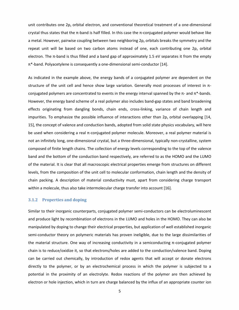
3.2 The operation scheme of an LEC
The active material in the basic configuration of an
LEC is composed of a light-emitting, semi-
conducting polymer, henceforth referred to as the
electroluminescent polymer, and an electrolyte.
Before subjected to a voltage bias and activated,
the material is presumed to be a uniform blend
and not electronically conductive. Figure 1 shows
the active material interposed between two
electrodes. There is, for the purpose of this
qualitative description, no need for specifying the
electrodes in any detail. For simplicity they are
depicted as made of metal and identical on both
sides, so that their Fermi levels, indicated by
dashed horizontal lines, are aligned when no
electric potential is applied. The solid lines illustrate
the lowest unoccupied molecular orbital (LUMO)
and the highest occupied molecular orbital (HOMO)
of the electroluminescent polymer. In this state of
the system charge injection is negligible as the
HOMO is filled and hardly any electrons have
enough thermal energy to reach the LUMO.
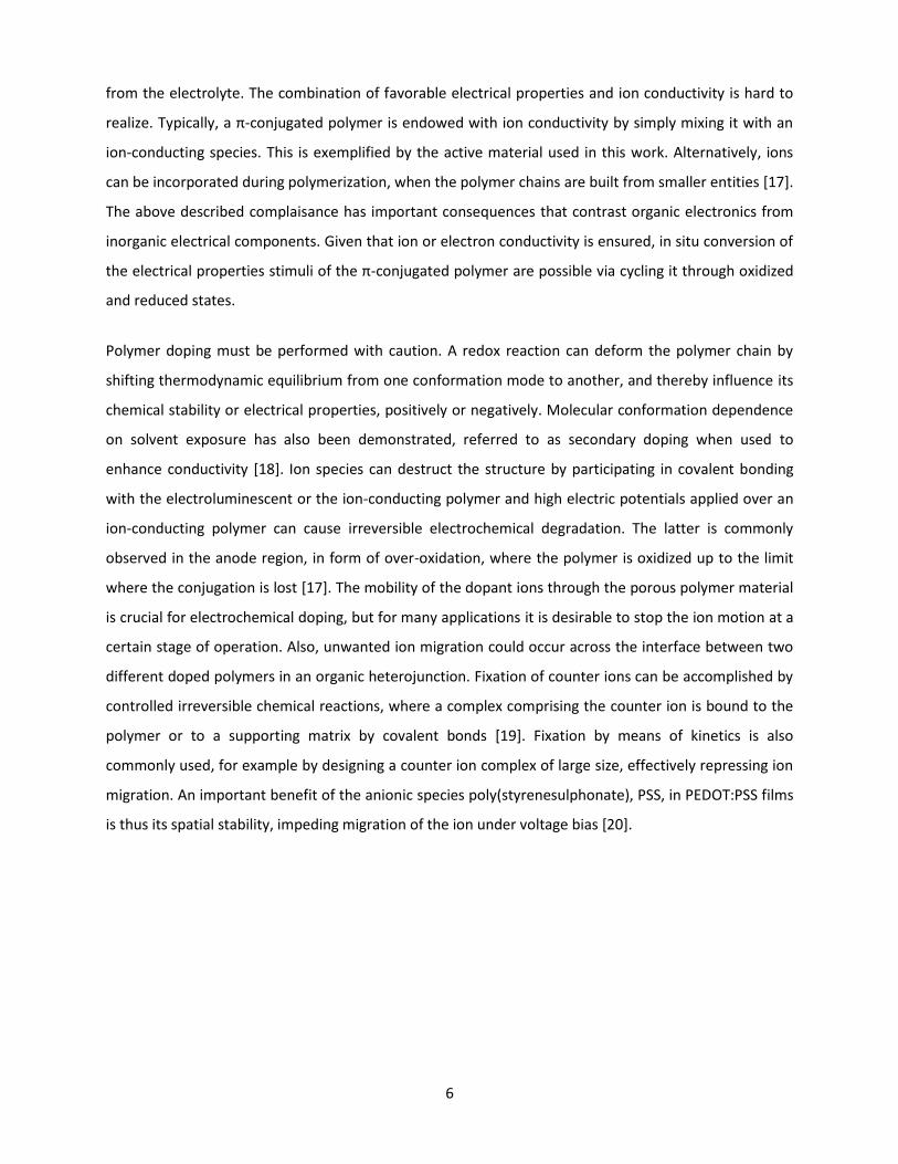
Immediately after applying a voltage bias, the
situation is as in Figure 3 where the electrostatic
potential profile in the active material layer is
indicated by the slope of the energy levels. The
difference in height between the electrode Fermi
levels corresponds to the applied external potential
and the potential gradient is constant across the
sandwiched material. Neither in this case is there
significant electron/hole injection, as the widths of
the energy barriers at the electrode interfaces are
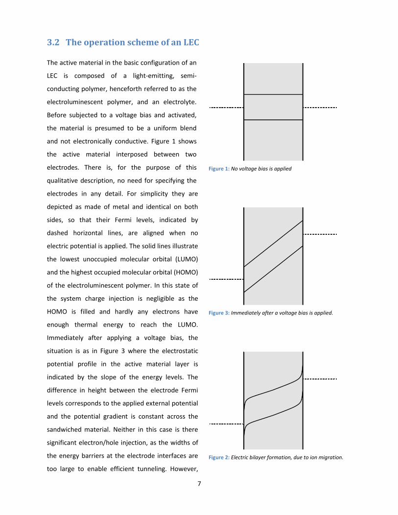
too large to enable efficient tunneling. However,
Figure 1: No voltage bias is applied
Figure 3: Immediately after a voltage bias is applied.
Figure 2: Electric bilayer formation, due to ion migration.
8
the applied electric potential exerts a force on the mobile ions in the electrolyte, which initiates ion
migration throughout the active material. Positively charged ions are pushed in one direction and
negatively charged ions in the other, congregating close to the electrode attracting them. The
electrostatic potential from the electrode is gradually screened as the ion concentration close to the
interface increases, forming an electrical double layer in the vicinity of the electrode surface. The
resulting energy levels are illustrated in Figure 2. Now, as the ion concentration increases in the
proximity of the metal surface, eventually the energy barrier width between the electrodes and the
enclosed material has shrunk sufficiently to enable significant electron/hole injection, into
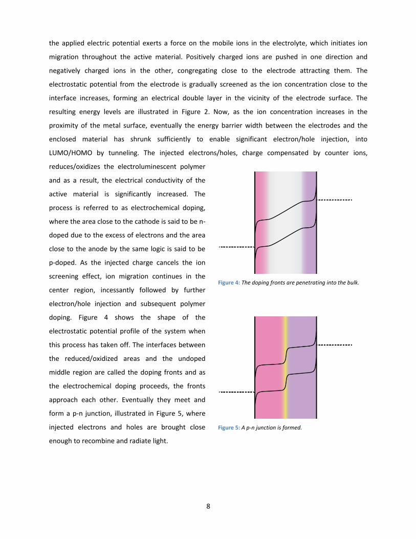
LUMO/HOMO by tunneling. The injected electrons/holes, charge compensated by counter ions,
reduces/oxidizes the electroluminescent polymer
and as a result, the electrical conductivity of the
active material is significantly increased. The
process is referred to as electrochemical doping,
where the area close to the cathode is said to be n-
doped due to the excess of electrons and the area
close to the anode by the same logic is said to be
p-doped. As the injected charge cancels the ion
screening effect, ion migration continues in the
center region, incessantly followed by further
electron/hole injection and subsequent polymer
doping. Figure 4 shows the shape of the
electrostatic potential profile of the system when
this process has taken off. The interfaces between
the reduced/oxidized areas and the undoped
middle region are called the doping fronts and as
the electrochemical doping proceeds, the fronts
approach each other. Eventually they meet and
form a p-n junction, illustrated in Figure 5, where
injected electrons and holes are brought close
enough to recombine and radiate light.
Figure 4: The doping fronts are penetrating into the bulk.
Figure 5: A p-n junction is formed.
9
3.3 Expected consequences on performance
Summarizing the course of events after subjecting
the active material to a voltage bias, there is ion
migration that gives rise to a double layer,
facilitating electron / hole injection, that will in
turn initiate a doping process of the
electroluminescent polymer starting from the
electrode faces and gradually penetrating into the
bulk to eventually form a p-n junction. For this
series of events to realize, many conditions must
be fulfilled, but most of the delicate physical and
chemical mechanisms describing the details are
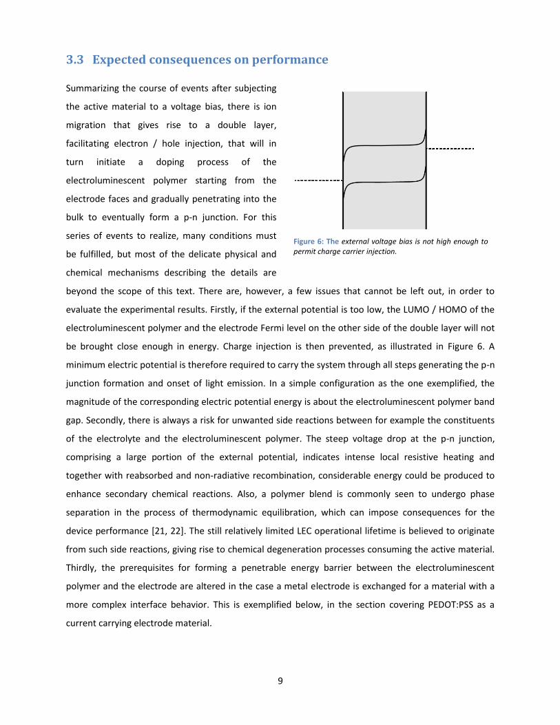
beyond the scope of this text. There are, however, a few issues that cannot be left out, in order to
evaluate the experimental results. Firstly, if the external potential is too low, the LUMO / HOMO of the
electroluminescent polymer and the electrode Fermi level on the other side of the double layer will not
be brought close enough in energy. Charge injection is then prevented, as illustrated in Figure 6. A
minimum electric potential is therefore required to carry the system through all steps generating the p-n
junction formation and onset of light emission. In a simple configuration as the one exemplified, the
magnitude of the corresponding electric potential energy is about the electroluminescent polymer band
gap. Secondly, there is always a risk for unwanted side reactions between for example the constituents
of the electrolyte and the electroluminescent polymer. The steep voltage drop at the p-n junction,
comprising a large portion of the external potential, indicates intense local resistive heating and
together with reabsorbed and non-radiative recombination, considerable energy could be produced to
enhance secondary chemical reactions. Also, a polymer blend is commonly seen to undergo phase
separation in the process of thermodynamic equilibration, which can impose consequences for the
device performance [21, 22]. The still relatively limited LEC operational lifetime is believed to originate
from such side reactions, giving rise to chemical degeneration processes consuming the active material.
Thirdly, the prerequisites for forming a penetrable energy barrier between the electroluminescent
polymer and the electrode are altered in the case a metal electrode is exchanged for a material with a
more complex interface behavior. This is exemplified below, in the section covering PEDOT:PSS as a
current carrying electrode material.
Figure 6: The external voltage bias is not high enough to permit charge carrier injection.
10
3.4 PEDOT:PSS
3.4.1 The conductive polyelectrolyte complex
Truly undoped PEDOT is a semiconductor under ambient conditions and is oxidized in order to become
electrically conductive. The oxidized state is stabilized by delocalization of the positive charge, not only
along the π-conjugated carbon chain, but over a large portion of the PEDOT subunit. There is no known
solvent in which the PEDOT polycation is soluble and to achieve a polymeric dispersion it must be
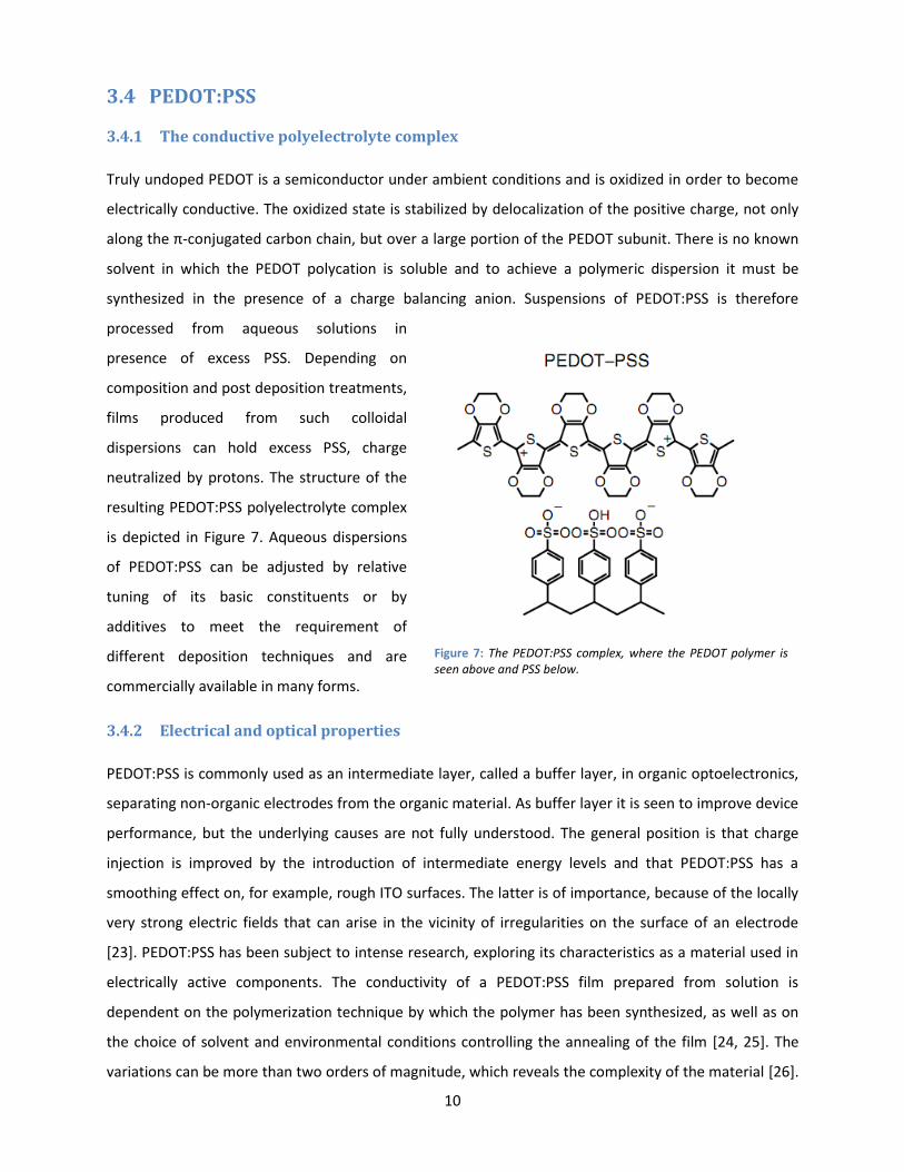
synthesized in the presence of a charge balancing anion. Suspensions of PEDOT:PSS is therefore
processed from aqueous solutions in
presence of excess PSS. Depending on
composition and post deposition treatments,
films produced from such colloidal
dispersions can hold excess PSS, charge
neutralized by protons. The structure of the
resulting PEDOT:PSS polyelectrolyte complex
is depicted in Figure 7. Aqueous dispersions
of PEDOT:PSS can be adjusted by relative
tuning of its basic constituents or by
additives to meet the requirement of
different deposition techniques and are
commercially available in many forms.
3.4.2 Electrical and optical properties
PEDOT:PSS is commonly used as an intermediate layer, called a buffer layer, in organic optoelectronics,
separating non-organic electrodes from the organic material. As buffer layer it is seen to improve device
performance, but the underlying causes are not fully understood. The general position is that charge
injection is improved by the introduction of intermediate energy levels and that PEDOT:PSS has a
smoothing effect on, for example, rough ITO surfaces. The latter is of importance, because of the locally
very strong electric fields that can arise in the vicinity of irregularities on the surface of an electrode
[23]. PEDOT:PSS has been subject to intense research, exploring its characteristics as a material used in
electrically active components. The conductivity of a PEDOT:PSS film prepared from solution is
dependent on the polymerization technique by which the polymer has been synthesized, as well as on
the choice of solvent and environmental conditions controlling the annealing of the film [24, 25]. The
variations can be more than two orders of magnitude, which reveals the complexity of the material [26].
Figure 7: The PEDOT:PSS complex, where the PEDOT polymer is seen above and PSS below.
11
Electrical conductivity in spin coated PEDOT:PSS films is seen to be anisotropic, where conductivity in
the plane of the substrate has been demonstrated to be about 500 times higher than in the normal
direction[27]. It is believed that the electrically conductive PEDOT and isolating PSS form spatially
separated domains in the nanometer size range within the bulk of PEDOT:PSS films. Both lamellar and
pancake-like morphologies have been proposed [28, 29]. Also, the volume fraction of PSS has been
observed to be larger at the film surface than in the bulk [28], which implies the existence of an energy
barrier for charge injection. Surface and interface phenomena are indeed important issues for the
function of PEDOT:PSS as an electrode and many electrochemical phenomena involving elements of the
PEDOT:PSS layer have been proposed to explain the degeneration of organic devices. Investigations of
the interface between PEDOT:PSS and organic semiconductors has revealed electronic shifts and
development of band bending, indicating a charge transfer [30]. The formation of such a dipole layer, on
the PEDOT:PSS side of the interface, has been interpreted in different ways. One suggestion is that a
formation of a layer of fixed dipoles is triggered by ionic bonding between anionic sulfonate moieties
not participating in the charge neutralized complex PEDOT:PSS, with cationic species of the neighboring
layer material [31]. The demonstrated drift of sodium cations, crossing the interface between a glass
substrate and the PEDOT:PSS layer is interesting as it points out the possibility of cation exchange
between the PEDOT:PSS layer and its surroundings [32]. Used as a hole injection layer in an OLED,
reduction of the oxidized PEDOT has been reported, possibly due to the diffusion of non-recombined
electrons through the active layer [33] or to ion content and acidity, expressed in the presence of water
[32, 34]. Summarizing, the role of possible degenerating side reactions involving PEDOT:PSS is not clear
and needs to be further investigated.
The suitability of a material as a current carrying electrode in a light-emitting device requires both high
transparency and conductivity. PEDOT is in its pristine state non conductive and the absorption
properties of the oxidized material must be investigated together with the counter ion of choice. In the
PEDOT:PSS complex its transparency in the visible region is increased with an increasing level of
oxidation, but at a certain limit, the continuous conductive pathways are disrupted and conductivity will
decline if the material is further oxidized [35]. Thus, if restricted to pure PEDOT:PSS, the electrochemical
stability window will circumscribe the possibilities of optimization due to doping level, but improvement
of conductivity can also be achieved by modifying morphology, as indicated in the section above, by
means of solvent treatment and annealing conditions. Incorporation of additives offer another route
towards simultaneous enhancement of optical transmission and conductivity in PEDOT:PSS based
conductive films [36-40]. As an example, Orgacon PEDOT:PSS, used in the experiments in this thesis, was

12
recently used together with a printed metallic structure to form large scale, printable anodes for ITO-
free devices [41].
13
4 Method
The development of the coaxial cell involves new combinations of materials as well as a change in
geometrical composition. In this section a reference point is defined and the course of stepwise
alteration is outlined.
4.1 The reference device
Producing LECs based on a conjugated
polymer as the active layer material is a
sophisticated procedure. A small change in
one of many variables, such as temperature
or concentration of contaminants in the
surrounding atmosphere during different
stages of fabrication, can largely influence
the final result. Nevertheless, evaluating
the performance of a structure of new composition requires a reference point as stable and high
performing as possible. Stability and well known characteristics help distinguish any emerging features
due to the change introduced in the system and a high performance decreases the influence of
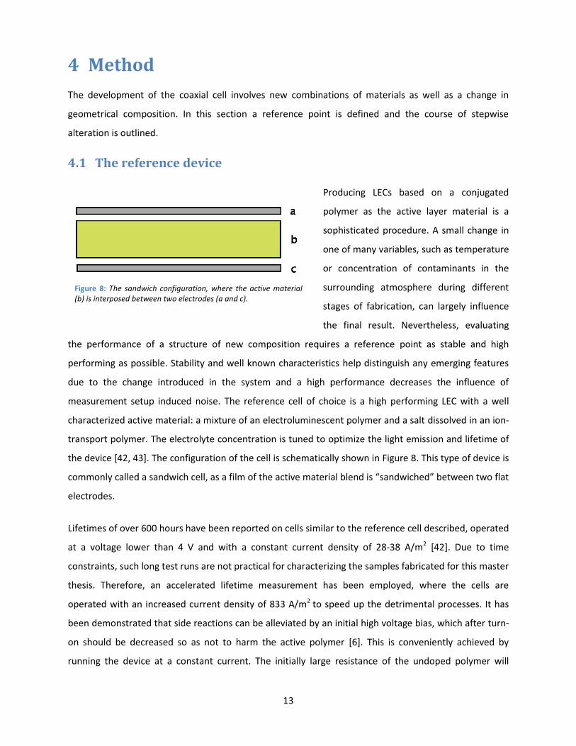
measurement setup induced noise. The reference cell of choice is a high performing LEC with a well
characterized active material: a mixture of an electroluminescent polymer and a salt dissolved in an ion-
transport polymer. The electrolyte concentration is tuned to optimize the light emission and lifetime of
the device [42, 43]. The configuration of the cell is schematically shown in Figure 8. This type of device is
commonly called a sandwich cell, as a film of the active material blend is “sandwiched” between two flat
electrodes.
Lifetimes of over 600 hours have been reported on cells similar to the reference cell described, operated
at a voltage lower than 4 V and with a constant current density of 28-38 A/m2 [42]. Due to time
constraints, such long test runs are not practical for characterizing the samples fabricated for this master
thesis. Therefore, an accelerated lifetime measurement has been employed, where the cells are
operated with an increased current density of 833 A/m2 to speed up the detrimental processes. It has
been demonstrated that side reactions can be alleviated by an initial high voltage bias, which after turn-
on should be decreased so as not to harm the active polymer [6]. This is conveniently achieved by
running the device at a constant current. The initially large resistance of the undoped polymer will
Figure 8: The sandwich configuration, where the active material (b) is interposed between two electrodes (a and c).

14
produce a high voltage, which automatically decreases along with decreasing resistance due to the
electrochemical doping of the electroluminescent polymer.
4.2 Replacing ITO for PEDOT:PSS
The choice of PEDOT:PSS as the substitute for ITO is motivated by the possibility of deposition from
solution, the availability and reasonably low price of the comprising elements comprising it, its flexibility
and its favorable electronic properties. In the application investigated here, electric current must pass
laterally through the layer of the electrode, in the plane of the film, to spread over the entire cell
surface. The lateral resistance of a thin and evenly spread film is called sheet-resistance and increases
with decreasing film thickness. However, as PEDOT:PSS is not completely transparent, increased film
thickness will also negatively influence the performance of the device due to increased absorption.
Considerations on how to achieve an even film of adequate thickness resulted in tests with thick single
layers of PEDOT:PSS as well as multiple thin layers, sequentially spin coated on top of each other. The
relative deposition order of PEDOT:PSS and the active layer can induce differences in charge injection
efficiency, due to the annealing process of the PEDOT:PSS film. Therefore samples were prepared in
both ways.
4.3 Changing geometry
Lastly, an LEC of coaxial geometry was produced, constructed on a core of gold supplying structural
support and serving as the cathode of the device. Both the active material and the PEDOT:PSS anode
was deposited to the gold wire by dip coating.
15
5 Experimental
Before presenting experiments and results, an introduction to the technical methods is given and the
materials and their preparation are described.
5.1 Means and materials
In addition to a description of the techniques and materials used for fabrication of devices, some
technical issues and their commonly used solutions are commented on. Also, the molecular structures of
the constituents in the active material are illustrated in the section where preparation of the active
material blend solution is described.
5.1.1 Cleaning
The solvents used for cleaning were detergent (Alkaline Extran MA01, Merck), acetone (technical grade,
VWR International) and 2-propanol (analysis grade, Merck). Substrates for LECs in a sandwich
configuration were cleaned by subsequent ultrasonic treatment in a 10:1 aqueous alkaline solution,
acetone and 2-propanol. Acetone was used for ultrasonic cleaning of glass vials and rinsing of glass Petri
dishes and tweezers. New glass pipettes, blown clean by nitrogen gas, were used for the application of
solutions onto substrates. Nitrogen gas was also used to remove dust both from the plastic caps sealing
the glass vials and from the surfaces of the substrates before every deposition of solution.
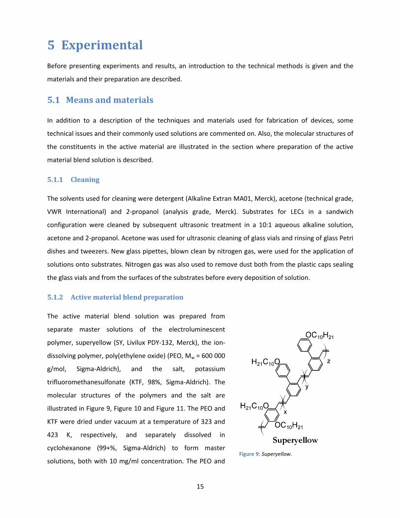
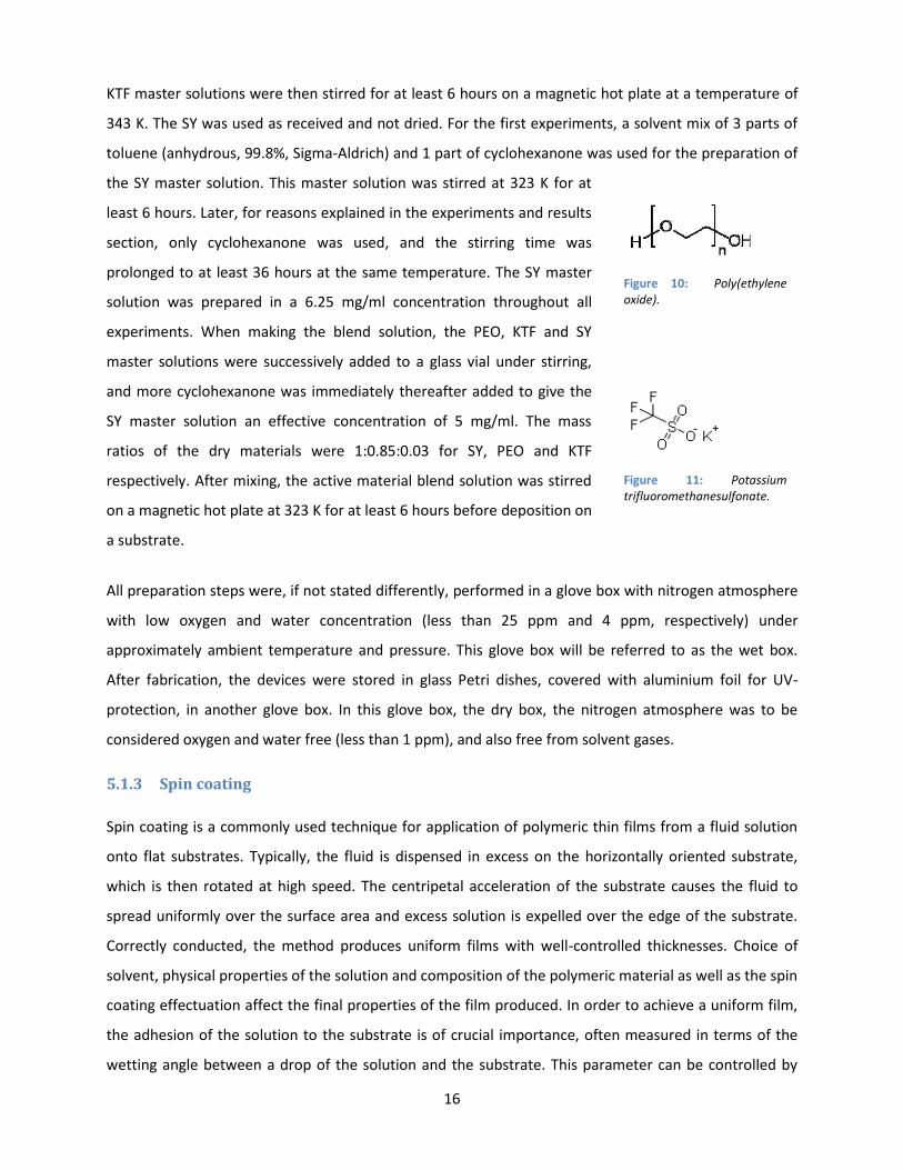
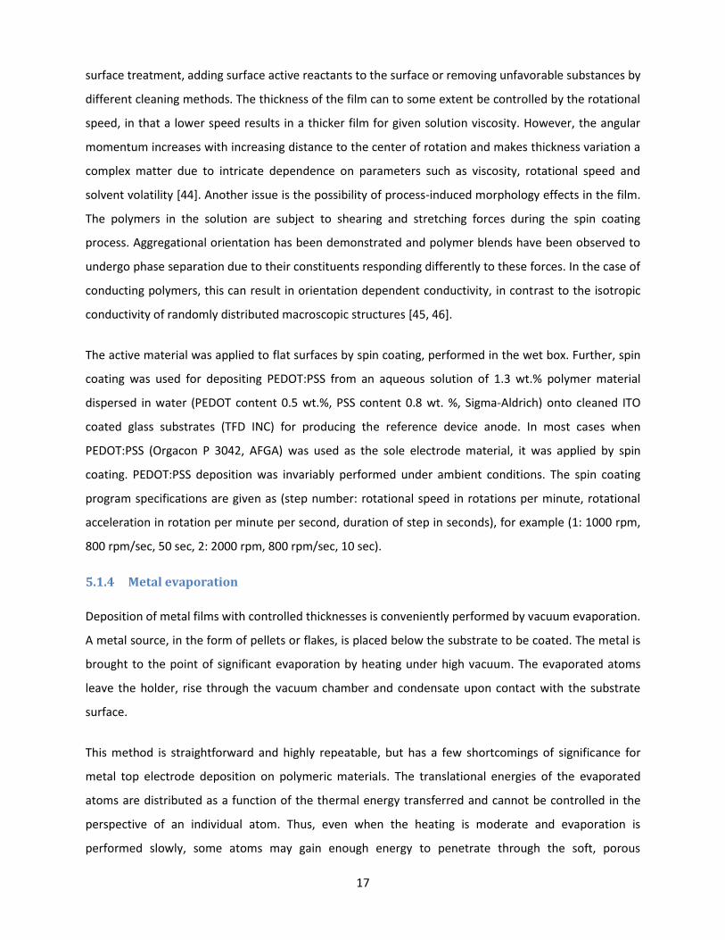
5.1.2 Active material blend preparation
The active material blend solution was prepared from
separate master solutions of the electroluminescent
polymer, superyellow (SY, Livilux PDY-132, Merck), the ion-
dissolving polymer, poly(ethylene oxide) (PEO, Mw = 600 000
g/mol, Sigma-Aldrich), and the salt, potassium
trifluoromethanesulfonate (KTF, 98%, Sigma-Aldrich). The
molecular structures of the polymers and the salt are
illustrated in Figure 9, Figure 10 and Figure 11. The PEO and
KTF were dried under vacuum at a temperature of 323 and
423 K, respectively, and separately dissolved in
cyclohexanone (99+%, Sigma-Aldrich) to form master
solutions, both with 10 mg/ml concentration. The PEO and
Figure 9: Superyellow.
16
KTF master solutions were then stirred for at least 6 hours on a magnetic hot plate at a temperature of
343 K. The SY was used as received and not dried. For the first experiments, a solvent mix of 3 parts of
toluene (anhydrous, 99.8%, Sigma-Aldrich) and 1 part of cyclohexanone was used for the preparation of
the SY master solution. This master solution was stirred at 323 K for at
least 6 hours. Later, for reasons explained in the experiments and results
section, only cyclohexanone was used, and the stirring time was
prolonged to at least 36 hours at the same temperature. The SY master
solution was prepared in a 6.25 mg/ml concentration throughout all
experiments. When making the blend solution, the PEO, KTF and SY
master solutions were successively added to a glass vial under stirring,
and more cyclohexanone was immediately thereafter added to give the
SY master solution an effective concentration of 5 mg/ml. The mass
ratios of the dry materials were 1:0.85:0.03 for SY, PEO and KTF
respectively. After mixing, the active material blend solution was stirred
on a magnetic hot plate at 323 K for at least 6 hours before deposition on
a substrate.
All preparation steps were, if not stated differently, performed in a glove box with nitrogen atmosphere
with low oxygen and water concentration (less than 25 ppm and 4 ppm, respectively) under
approximately ambient temperature and pressure. This glove box will be referred to as the wet box.
After fabrication, the devices were stored in glass Petri dishes, covered with aluminium foil for UV-
protection, in another glove box. In this glove box, the dry box, the nitrogen atmosphere was to be
considered oxygen and water free (less than 1 ppm), and also free from solvent gases.
5.1.3 Spin coating
Spin coating is a commonly used technique for application of polymeric thin films from a fluid solution
onto flat substrates. Typically, the fluid is dispensed in excess on the horizontally oriented substrate,
which is then rotated at high speed. The centripetal acceleration of the substrate causes the fluid to
spread uniformly over the surface area and excess solution is expelled over the edge of the substrate.
Correctly conducted, the method produces uniform films with well-controlled thicknesses. Choice of
solvent, physical properties of the solution and composition of the polymeric material as well as the spin
coating effectuation affect the final properties of the film produced. In order to achieve a uniform film,
the adhesion of the solution to the substrate is of crucial importance, often measured in terms of the
wetting angle between a drop of the solution and the substrate. This parameter can be controlled by
Figure 10: Poly(ethylene oxide).
Figure 11: Potassium trifluoromethanesulfonate.
17
surface treatment, adding surface active reactants to the surface or removing unfavorable substances by
different cleaning methods. The thickness of the film can to some extent be controlled by the rotational
speed, in that a lower speed results in a thicker film for given solution viscosity. However, the angular
momentum increases with increasing distance to the center of rotation and makes thickness variation a
complex matter due to intricate dependence on parameters such as viscosity, rotational speed and
solvent volatility [44]. Another issue is the possibility of process-induced morphology effects in the film.
The polymers in the solution are subject to shearing and stretching forces during the spin coating
process. Aggregational orientation has been demonstrated and polymer blends have been observed to
undergo phase separation due to their constituents responding differently to these forces. In the case of
conducting polymers, this can result in orientation dependent conductivity, in contrast to the isotropic
conductivity of randomly distributed macroscopic structures [45, 46].
The active material was applied to flat surfaces by spin coating, performed in the wet box. Further, spin
coating was used for depositing PEDOT:PSS from an aqueous solution of 1.3 wt.% polymer material
dispersed in water (PEDOT content 0.5 wt.%, PSS content 0.8 wt. %, Sigma-Aldrich) onto cleaned ITO
coated glass substrates (TFD INC) for producing the reference device anode. In most cases when
PEDOT:PSS (Orgacon P 3042, AFGA) was used as the sole electrode material, it was applied by spin
coating. PEDOT:PSS deposition was invariably performed under ambient conditions. The spin coating
program specifications are given as (step number: rotational speed in rotations per minute, rotational
acceleration in rotation per minute per second, duration of step in seconds), for example (1: 1000 rpm,
800 rpm/sec, 50 sec, 2: 2000 rpm, 800 rpm/sec, 10 sec).
5.1.4 Metal evaporation
Deposition of metal films with controlled thicknesses is conveniently performed by vacuum evaporation.
A metal source, in the form of pellets or flakes, is placed below the substrate to be coated. The metal is
brought to the point of significant evaporation by heating under high vacuum. The evaporated atoms
leave the holder, rise through the vacuum chamber and condensate upon contact with the substrate
surface.
This method is straightforward and highly repeatable, but has a few shortcomings of significance for
metal top electrode deposition on polymeric materials. The translational energies of the evaporated
atoms are distributed as a function of the thermal energy transferred and cannot be controlled in the
perspective of an individual atom. Thus, even when the heating is moderate and evaporation is
performed slowly, some atoms may gain enough energy to penetrate through the soft, porous
18
polymeric material. A high degree of penetration can result in conducting pathways through the active
layer which will, when the device is subjected to a voltage bias, cause electrical short-circuiting. One
strategy to decrease negative effects of inter-diffusion is the use of aptly reactive metals, rather than
inert ones, in order to chemically lock the evaporated atoms to the surface of the target material and
form a protecting layer, preventing penetration of subsequent atoms. The idea is frequently used and
referred to as capping layer formation. Aluminium, forming an aluminium oxide capping layer at the
polymer interface, can be used as evaporated metal top electrode in organic electronics [47]. However,
high chemical reactivity imposes a risk for unwanted side reactions. Also, aluminium oxide is electrically
insulating and introduces a charge injection barrier. Therefore inert metals such as gold are preferred
when possible.
Aluminium (Al, 99.999%, Umicore) was chosen for fabrication of all devices with metal top electrode. As
aluminium is readily oxidized under positive bias, the aluminium electrode must be used as the negative
cathode. When the order of layer deposition was reversed, putting the metal electrode on the bottom,
experiments were performed with both gold (Au, 99.99%, Kurt J. Lesker Company) and aluminium as the
electrode metal. In order to make the gold layer stick to the glass substrate, a 10 nm layer of chromium
(Cr, 99.99%, Umicore) was first evaporated onto the glass surface. Several devices could be fabricated
on the same substrate, by evaporation through a shadow mask.
5.1.5 Measurement conditions
The device performance measurements were accomplished in the dry box, where the samples were
mounted in a measurement box. Light emission was recorded with a photodiode with eye response
filter, and the data was saved directly on a PC, together with recorded values of current and potential
bias. Unfortunately, some technical issues were encountered, for instance the transfer of photodiode
information to the PC. Connection failure was expressed as periods of time when zero light emission was
falsely recorded. The measurement recordings presented in the experimental part were, for clarity,
chosen among the plots that were not affected to a great extent, but the issue is occasionally
manifested as sharply interrupted light emission curves.
19
5.2 Experiments and results
No preceding results have been found in the literature for the specific combination of electrode and
active layer material used in this thesis. The set of experiments could therefore not be planned in detail
as the outcome of one experiment would frame the design of the following. In order to clarify the logic
connecting ensuing steps, results will be presented and discussed chronologically. Unforeseen problems
of special interest that arose during the course of the experimental work are reported.
5.2.1 Reference device
The SY master solution used for the first batch of
reference devices was based on a mix of toluene
and cyclohexanone, deposited by spin coating
(1: 800 rpm, 800 rpm/sec, 50 sec, 2: 2000 rpm,
800 rpm/sec, 10 sec). To minimize the sheet
resistance, the aluminium top electrodes were
made thick, about 60 nm. The ITO coated glass
substrates were spin coated with a thin layer of
PEDOT:PSS (1: 4000 rpm, 1000 rpm/sec, 60 sec).
This fabrication step proved non-trivial. The
solution adhesion to the substrate surface
seemed to differ from day to day, in spite of very
exact repetition of all parts of the procedure,
such as cleaning of the substrates. It was
observed that the quality of the produced films was enhanced by low relative air humidity, but no
systematic investigations were made on this subject. A schematic picture of the device is depicted in
Figure 12, the arrow pointing in the direction of light effluence.
The performance of the devices were in accordance with previous experience [42] and the data from a
typical measurement is represented in Figure 13, were the light output and voltage drop are plotted as a
function of time. The best devices gave a maximum light emission exceeding 2000 cd/m2 and had a
lifetime of more than ten hours.
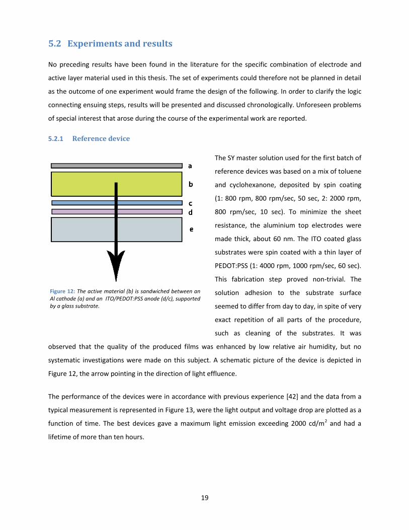
Figure 12: The active material (b) is sandwiched between an Al cathode (a) and an ITO/PEDOT:PSS anode (d/c), supported by a glass substrate.
20
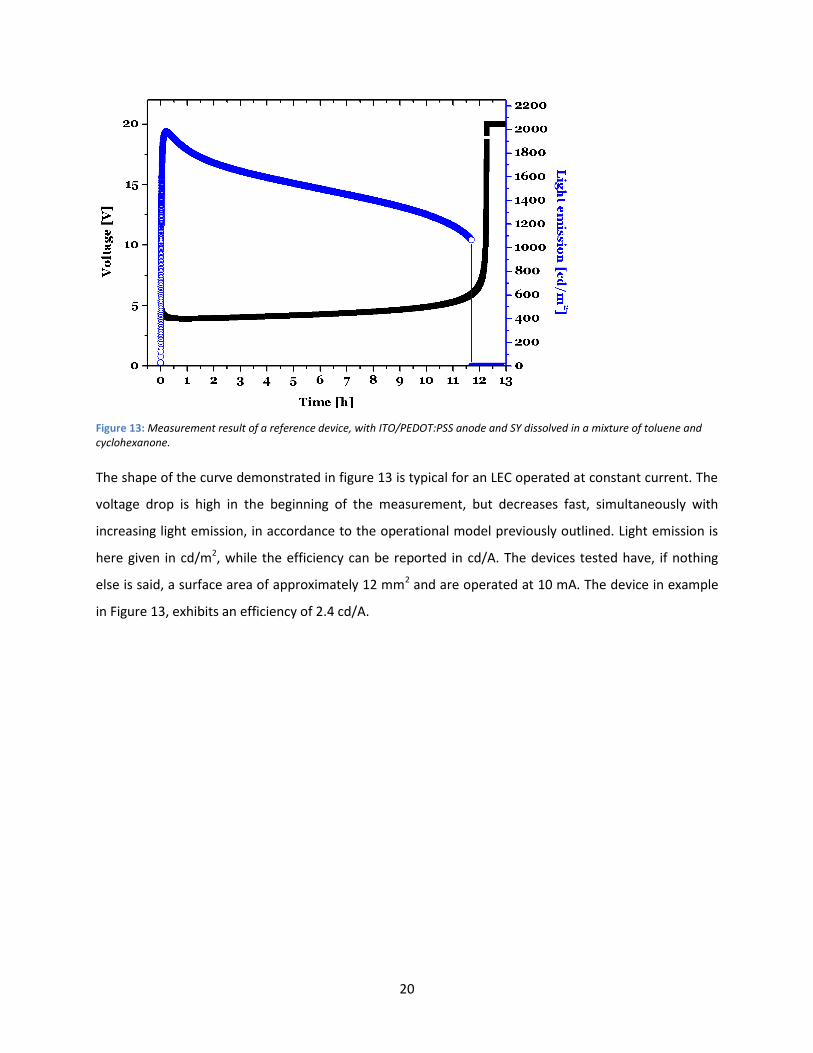
Figure 13: Measurement result of a reference device, with ITO/PEDOT:PSS anode and SY dissolved in a mixture of toluene and cyclohexanone.
The shape of the curve demonstrated in figure 13 is typical for an LEC operated at constant current. The
voltage drop is high in the beginning of the measurement, but decreases fast, simultaneously with
increasing light emission, in accordance to the operational model previously outlined. Light emission is
here given in cd/m2, while the efficiency can be reported in cd/A. The devices tested have, if nothing
else is said, a surface area of approximately 12 mm2 and are operated at 10 mA. The device in example
in Figure 13, exhibits an efficiency of 2.4 cd/A.
21
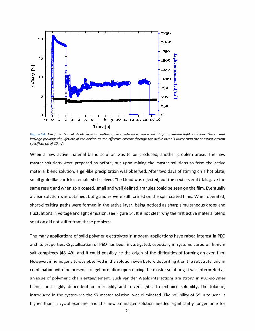
Figure 14: The formation of short-circuiting pathways in a reference device with high maximum light emission. The current leakage prolongs the lifetime of the device, as the effective current through the active layer is lower than the constant current specification of 10 mA.
When a new active material blend solution was to be produced, another problem arose. The new
master solutions were prepared as before, but upon mixing the master solutions to form the active
material blend solution, a gel-like precipitation was observed. After two days of stirring on a hot plate,
small grain-like particles remained dissolved. The blend was rejected, but the next several trials gave the
same result and when spin coated, small and well defined granules could be seen on the film. Eventually
a clear solution was obtained, but granules were still formed on the spin coated films. When operated,
short-circuiting paths were formed in the active layer, being noticed as sharp simultaneous drops and
fluctuations in voltage and light emission; see Figure 14. It is not clear why the first active material blend
solution did not suffer from these problems.
The many applications of solid polymer electrolytes in modern applications have raised interest in PEO
and its properties. Crystallization of PEO has been investigated, especially in systems based on lithium
salt complexes [48, 49], and it could possibly be the origin of the difficulties of forming an even film.
However, inhomogeneity was observed in the solution even before depositing it on the substrate, and in
combination with the presence of gel formation upon mixing the master solutions, it was interpreted as
an issue of polymeric chain entanglement. Such van der Waals interactions are strong in PEO-polymer
blends and highly dependent on miscibility and solvent [50]. To enhance solubility, the toluene,
introduced in the system via the SY master solution, was eliminated. The solubility of SY in toluene is
higher than in cyclohexanone, and the new SY master solution needed significantly longer time for
22
preparation. The result was however encouraging as the active material blend solution prepared was
clear and gave smooth films.
During the fabrication of devices from the new
active material blend, dissolved in pure
cyclohexanone, the spin coating of smoothing
PEDOT:PSS layers on the ITO-coated substrates
delivered very poor results. To be able to
continue the investigations, it was decided that
the PEDOT:PSS layer was to be omitted from
the reference devices. The resulting devices,
schematically illustrated in Figure 15, showed
somewhat worse performance than the
former. This might be related to the roughness
of the ITO-layer, but also to possible influences
of the atmospheric conditions, as over 20 ppm oxygen was recorded several times during solution
preparation, spin coating and annealing. The possibility of morphology changes in the active material,
due to the change of solvent composition was also considered. Adjustments of the spin coating program
resulted in better performance and higher repeatability, and a program specification was decided on (1:
1500 rpm, 1000 rpm/sec, 60 sec), which was then used for active layer material deposition on all
devices. Unfortunately, the high performance of the former devices was not reached. Maximum light
emission of more than 2000 cd/m2 was measured only a few times and the devices deteriorated faster,
in about 6 hours. Still, the overall shape of the measurement curves was unchanged. A measurement
result, representative in light emission strength and shape of the curve but with unusually long lifetime,
is given in Figure 16.
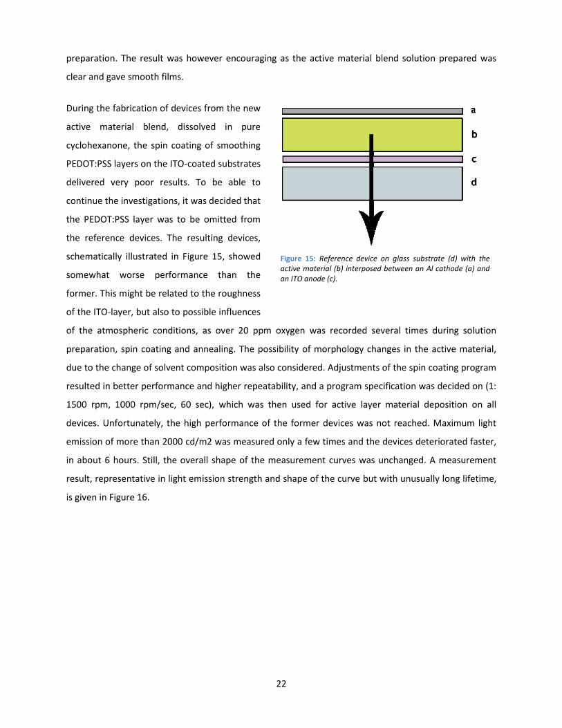
Figure 15: Reference device on glass substrate (d) with the active material (b) interposed between an Al cathode (a) and an ITO anode (c).
23
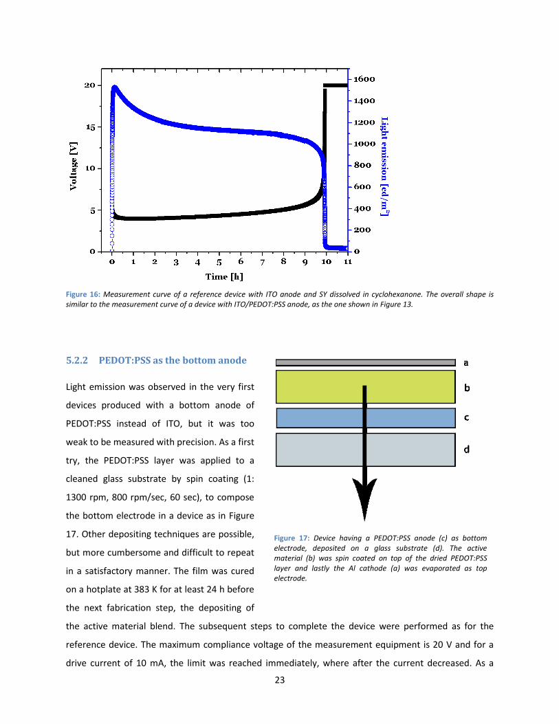
Figure 16: Measurement curve of a reference device with ITO anode and SY dissolved in cyclohexanone. The overall shape is similar to the measurement curve of a device with ITO/PEDOT:PSS anode, as the one shown in Figure 13.
5.2.2 PEDOT:PSS as the bottom anode
Light emission was observed in the very first
devices produced with a bottom anode of
PEDOT:PSS instead of ITO, but it was too
weak to be measured with precision. As a first
try, the PEDOT:PSS layer was applied to a
cleaned glass substrate by spin coating (1:
1300 rpm, 800 rpm/sec, 60 sec), to compose
the bottom electrode in a device as in Figure
17. Other depositing techniques are possible,
but more cumbersome and difficult to repeat
in a satisfactory manner. The film was cured
on a hotplate at 383 K for at least 24 h before
the next fabrication step, the depositing of
the active material blend. The subsequent steps to complete the device were performed as for the
reference device. The maximum compliance voltage of the measurement equipment is 20 V and for a
drive current of 10 mA, the limit was reached immediately, where after the current decreased. As a
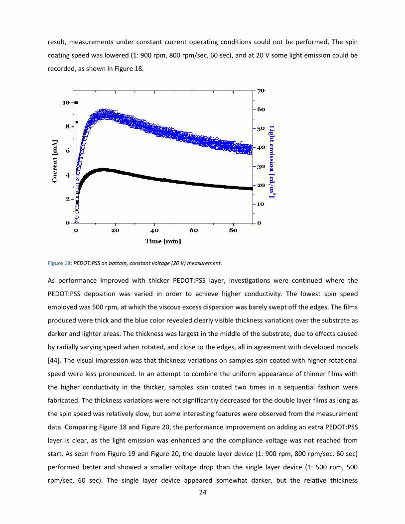
Figure 17: Device having a PEDOT:PSS anode (c) as bottom electrode, deposited on a glass substrate (d). The active material (b) was spin coated on top of the dried PEDOT:PSS layer and lastly the Al cathode (a) was evaporated as top electrode.
24
result, measurements under constant current operating conditions could not be performed. The spin
coating speed was lowered (1: 900 rpm, 800 rpm/sec, 60 sec), and at 20 V some light emission could be
recorded, as shown in Figure 18.
Figure 18: PEDOT:PSS on bottom, constant voltage (20 V) measurement.
As performance improved with thicker PEDOT:PSS layer, investigations were continued where the
PEDOT:PSS deposition was varied in order to achieve higher conductivity. The lowest spin speed
employed was 500 rpm, at which the viscous excess dispersion was barely swept off the edges. The films
produced were thick and the blue color revealed clearly visible thickness variations over the substrate as
darker and lighter areas. The thickness was largest in the middle of the substrate, due to effects caused
by radially varying speed when rotated, and close to the edges, all in agreement with developed models
[44]. The visual impression was that thickness variations on samples spin coated with higher rotational
speed were less pronounced. In an attempt to combine the uniform appearance of thinner films with
the higher conductivity in the thicker, samples spin coated two times in a sequential fashion were
fabricated. The thickness variations were not significantly decreased for the double layer films as long as
the spin speed was relatively slow, but some interesting features were observed from the measurement
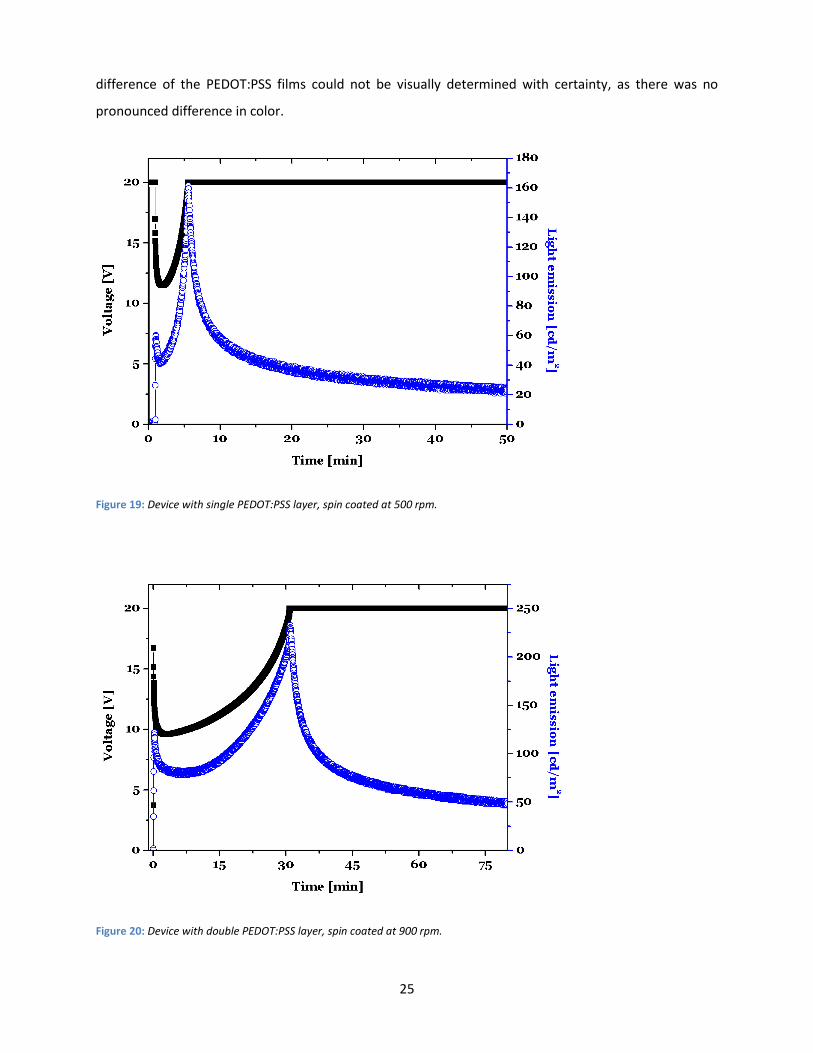
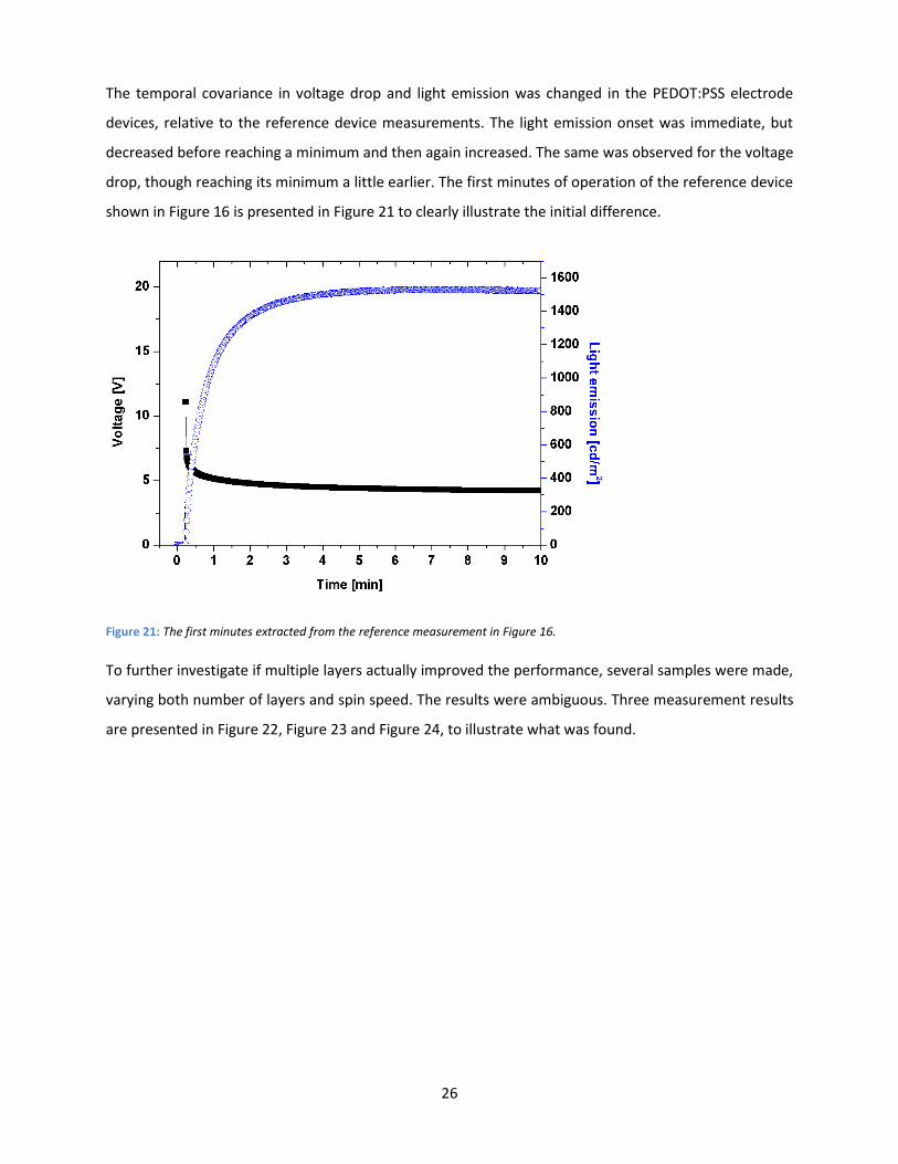
data. Comparing Figure 18 and Figure 20, the performance improvement on adding an extra PEDOT:PSS
layer is clear, as the light emission was enhanced and the compliance voltage was not reached from
start. As seen from Figure 19 and Figure 20, the double layer device (1: 900 rpm, 800 rpm/sec, 60 sec)
performed better and showed a smaller voltage drop than the single layer device (1: 500 rpm, 500
rpm/sec, 60 sec). The single layer device appeared somewhat darker, but the relative thickness
25
difference of the PEDOT:PSS films could not be visually determined with certainty, as there was no
pronounced difference in color.
Figure 19: Device with single PEDOT:PSS layer, spin coated at 500 rpm.
Figure 20: Device with double PEDOT:PSS layer, spin coated at 900 rpm.
26
The temporal covariance in voltage drop and light emission was changed in the PEDOT:PSS electrode
devices, relative to the reference device measurements. The light emission onset was immediate, but
decreased before reaching a minimum and then again increased. The same was observed for the voltage
drop, though reaching its minimum a little earlier. The first minutes of operation of the reference device
shown in Figure 16 is presented in Figure 21 to clearly illustrate the initial difference.
Figure 21: The first minutes extracted from the reference measurement in Figure 16.
To further investigate if multiple layers actually improved the performance, several samples were made,
varying both number of layers and spin speed. The results were ambiguous. Three measurement results
are presented in Figure 22, Figure 23 and Figure 24, to illustrate what was found.
27
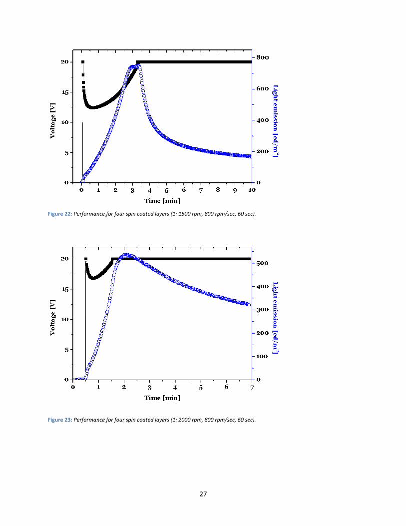
Figure 22: Performance for four spin coated layers (1: 1500 rpm, 800 rpm/sec, 60 sec).
Figure 23: Performance for four spin coated layers (1: 2000 rpm, 800 rpm/sec, 60 sec).
28
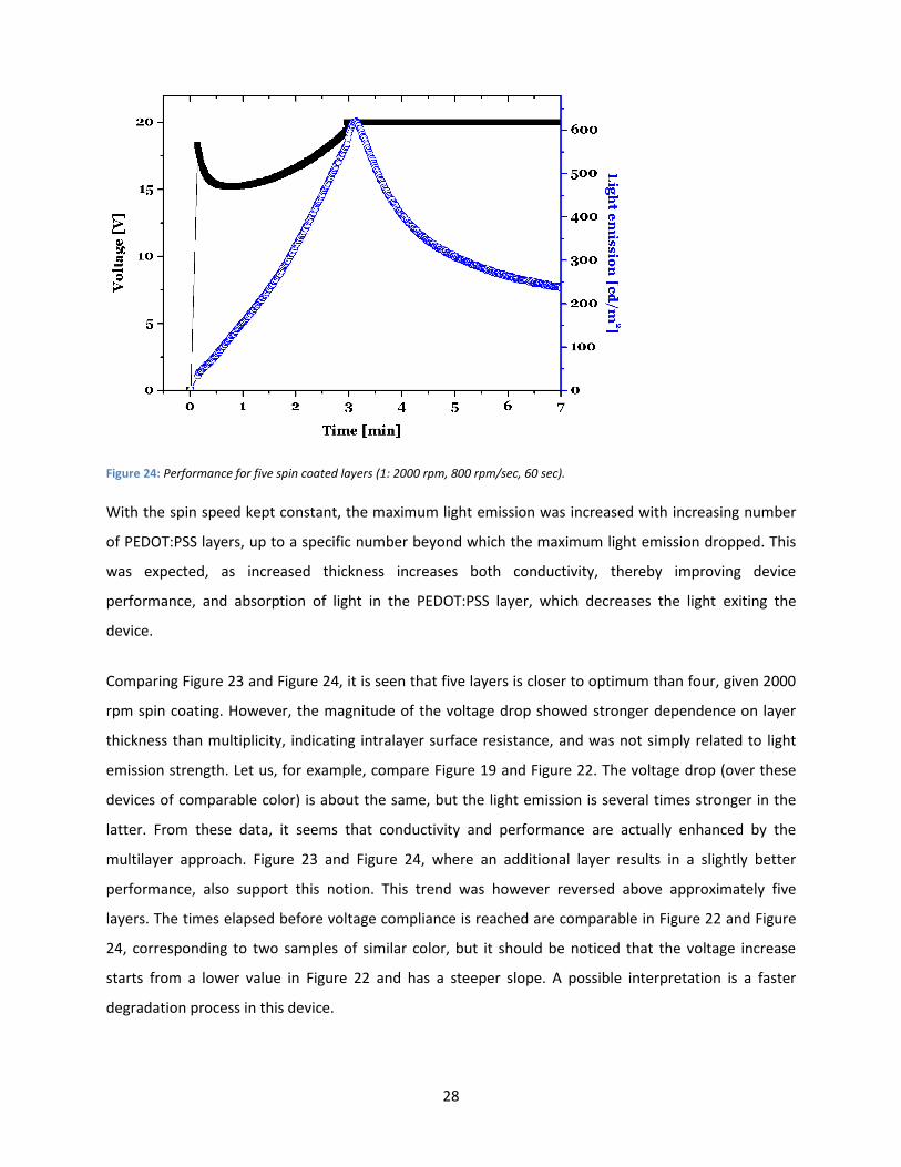
Figure 24: Performance for five spin coated layers (1: 2000 rpm, 800 rpm/sec, 60 sec).
With the spin speed kept constant, the maximum light emission was increased with increasing number
of PEDOT:PSS layers, up to a specific number beyond which the maximum light emission dropped. This
was expected, as increased thickness increases both conductivity, thereby improving device
performance, and absorption of light in the PEDOT:PSS layer, which decreases the light exiting the
device.
Comparing Figure 23 and Figure 24, it is seen that five layers is closer to optimum than four, given 2000
rpm spin coating. However, the magnitude of the voltage drop showed stronger dependence on layer
thickness than multiplicity, indicating intralayer surface resistance, and was not simply related to light
emission strength. Let us, for example, compare Figure 19 and Figure 22. The voltage drop (over these
devices of comparable color) is about the same, but the light emission is several times stronger in the
latter. From these data, it seems that conductivity and performance are actually enhanced by the
multilayer approach. Figure 23 and Figure 24, where an additional layer results in a slightly better
performance, also support this notion. This trend was however reversed above approximately five
layers. The times elapsed before voltage compliance is reached are comparable in Figure 22 and Figure
24, corresponding to two samples of similar color, but it should be noticed that the voltage increase
starts from a lower value in Figure 22 and has a steeper slope. A possible interpretation is a faster
degradation process in this device.
29
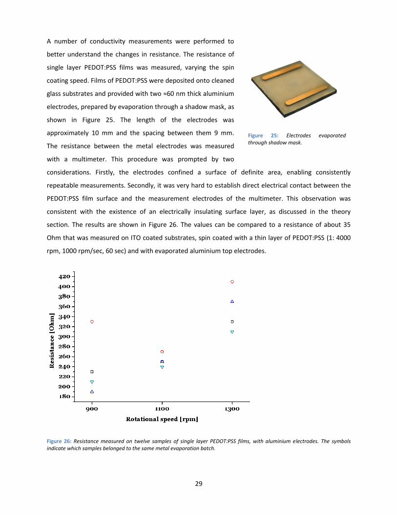
A number of conductivity measurements were performed to
better understand the changes in resistance. The resistance of
single layer PEDOT:PSS films was measured, varying the spin
coating speed. Films of PEDOT:PSS were deposited onto cleaned
glass substrates and provided with two ≈60 nm thick aluminium
electrodes, prepared by evaporation through a shadow mask, as
shown in Figure 25. The length of the electrodes was
approximately 10 mm and the spacing between them 9 mm.
The resistance between the metal electrodes was measured
with a multimeter. This procedure was prompted by two
considerations. Firstly, the electrodes confined a surface of definite area, enabling consistently
repeatable measurements. Secondly, it was very hard to establish direct electrical contact between the
PEDOT:PSS film surface and the measurement electrodes of the multimeter. This observation was
consistent with the existence of an electrically insulating surface layer, as discussed in the theory
section. The results are shown in Figure 26. The values can be compared to a resistance of about 35
Ohm that was measured on ITO coated substrates, spin coated with a thin layer of PEDOT:PSS (1: 4000
rpm, 1000 rpm/sec, 60 sec) and with evaporated aluminium top electrodes.
Figure 26: Resistance measured on twelve samples of single layer PEDOT:PSS films, with aluminium electrodes. The symbols indicate which samples belonged to the same metal evaporation batch.
Figure 25: Electrodes evaporated through shadow mask.
30
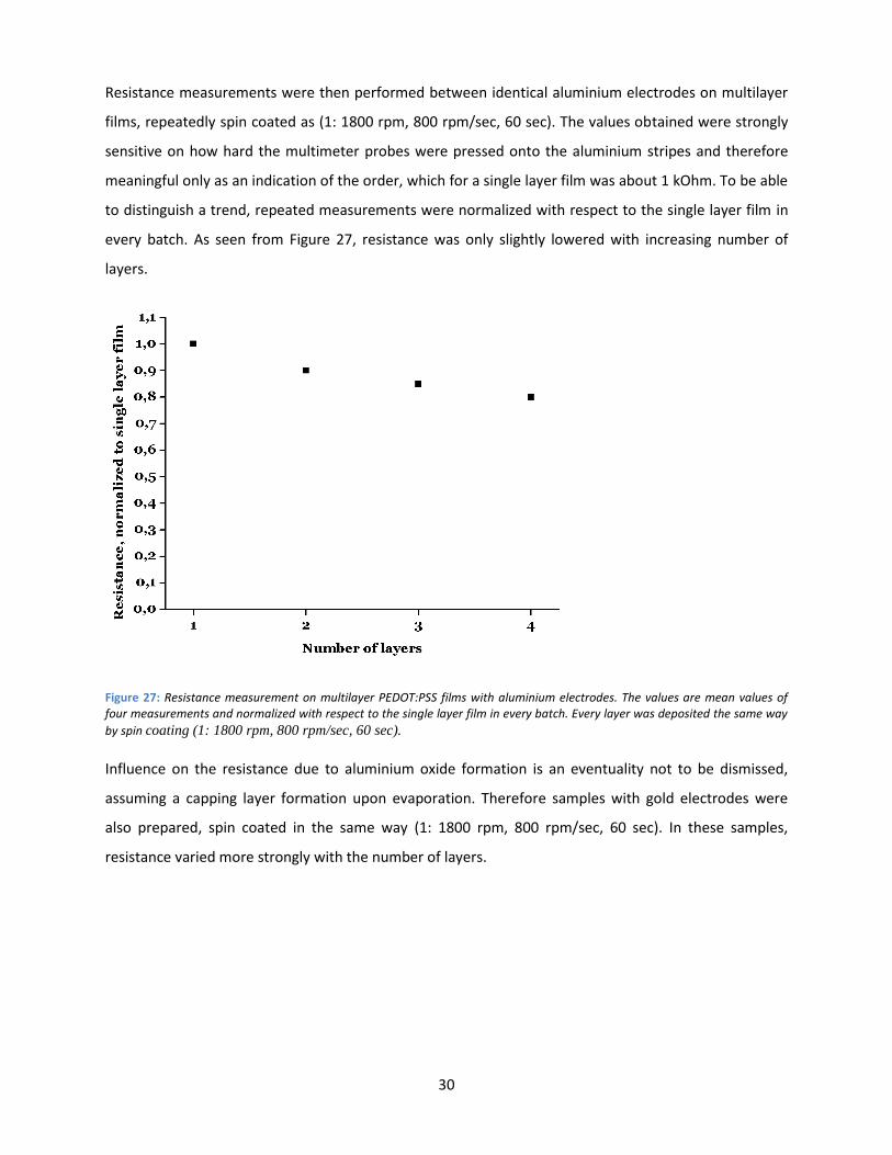
Resistance measurements were then performed between identical aluminium electrodes on multilayer
films, repeatedly spin coated as (1: 1800 rpm, 800 rpm/sec, 60 sec). The values obtained were strongly
sensitive on how hard the multimeter probes were pressed onto the aluminium stripes and therefore
meaningful only as an indication of the order, which for a single layer film was about 1 kOhm. To be able
to distinguish a trend, repeated measurements were normalized with respect to the single layer film in
every batch. As seen from Figure 27, resistance was only slightly lowered with increasing number of
layers.
Figure 27: Resistance measurement on multilayer PEDOT:PSS films with aluminium electrodes. The values are mean values of four measurements and normalized with respect to the single layer film in every batch. Every layer was deposited the same way
by spin coating (1: 1800 rpm, 800 rpm/sec, 60 sec).
Influence on the resistance due to aluminium oxide formation is an eventuality not to be dismissed,
assuming a capping layer formation upon evaporation. Therefore samples with gold electrodes were
also prepared, spin coated in the same way (1: 1800 rpm, 800 rpm/sec, 60 sec). In these samples,
resistance varied more strongly with the number of layers.
31
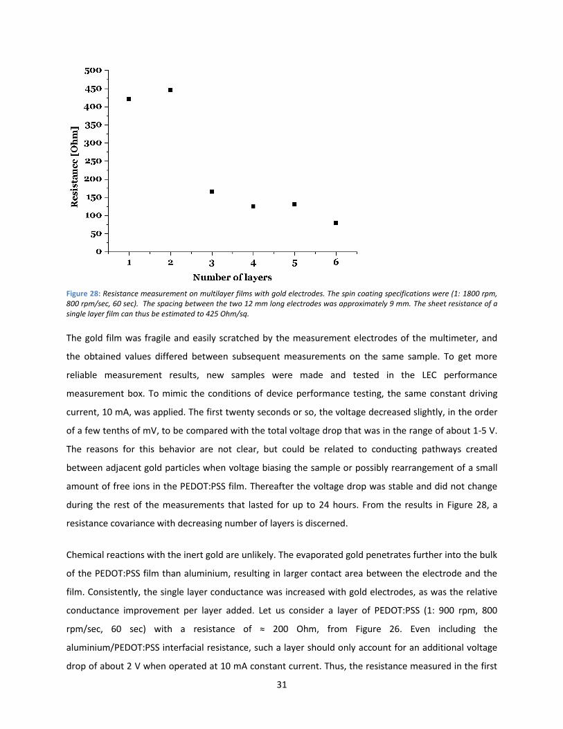
Figure 28: Resistance measurement on multilayer films with gold electrodes. The spin coating specifications were (1: 1800 rpm, 800 rpm/sec, 60 sec). The spacing between the two 12 mm long electrodes was approximately 9 mm. The sheet resistance of a single layer film can thus be estimated to 425 Ohm/sq.
The gold film was fragile and easily scratched by the measurement electrodes of the multimeter, and
the obtained values differed between subsequent measurements on the same sample. To get more
reliable measurement results, new samples were made and tested in the LEC performance
measurement box. To mimic the conditions of device performance testing, the same constant driving
current, 10 mA, was applied. The first twenty seconds or so, the voltage decreased slightly, in the order
of a few tenths of mV, to be compared with the total voltage drop that was in the range of about 1-5 V.
The reasons for this behavior are not clear, but could be related to conducting pathways created
between adjacent gold particles when voltage biasing the sample or possibly rearrangement of a small
amount of free ions in the PEDOT:PSS film. Thereafter the voltage drop was stable and did not change
during the rest of the measurements that lasted for up to 24 hours. From the results in Figure 28, a
resistance covariance with decreasing number of layers is discerned.
Chemical reactions with the inert gold are unlikely. The evaporated gold penetrates further into the bulk
of the PEDOT:PSS film than aluminium, resulting in larger contact area between the electrode and the
film. Consistently, the single layer conductance was increased with gold electrodes, as was the relative
conductance improvement per layer added. Let us consider a layer of PEDOT:PSS (1: 900 rpm, 800
rpm/sec, 60 sec) with a resistance of ≈ 200 Ohm, from Figure 26. Even including the
aluminium/PEDOT:PSS interfacial resistance, such a layer should only account for an additional voltage
drop of about 2 V when operated at 10 mA constant current. Thus, the resistance measured in the first
32
device performance tests, as seen in Figure 18, is much too high. Assuming an insignificant influence of
chemical degeneration processes when the voltage is at its minimum, the interfacial resistance between
PEDOT:PSS and the active layer material must thus be larger than between PEDOT:PSS and aluminium.
This could possibly be due to salt-like dipole formations at the organic heterojunction [31]. It might also
be a consequence of the surface energies and their influence on morphology and molecular
conformation of the polymers in the active material blend, when applied to the PEDOT:PSS surface.
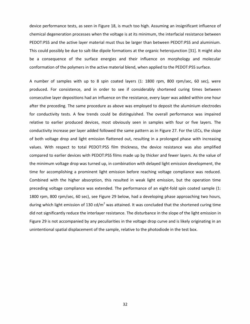
A number of samples with up to 8 spin coated layers (1: 1800 rpm, 800 rpm/sec, 60 sec), were
produced. For consistence, and in order to see if considerably shortened curing times between
consecutive layer depositions had an influence on the resistance, every layer was added within one hour
after the preceding. The same procedure as above was employed to deposit the aluminium electrodes
for conductivity tests. A few trends could be distinguished. The overall performance was impaired
relative to earlier produced devices, most obviously seen in samples with four or five layers. The
conductivity increase per layer added followed the same pattern as in Figure 27. For the LECs, the slope
of both voltage drop and light emission flattened out, resulting in a prolonged phase with increasing
values. With respect to total PEDOT:PSS film thickness, the device resistance was also amplified
compared to earlier devices with PEDOT:PSS films made up by thicker and fewer layers. As the value of
the minimum voltage drop was turned up, in combination with delayed light emission development, the
time for accomplishing a prominent light emission before reaching voltage compliance was reduced.
Combined with the higher absorption, this resulted in weak light emission, but the operation time
preceding voltage compliance was extended. The performance of an eight-fold spin coated sample (1:
1800 rpm, 800 rpm/sec, 60 sec), see Figure 29 below, had a developing phase approaching two hours,
during which light emission of 130 cd/m2 was attained. It was concluded that the shortened curing time
did not significantly reduce the interlayer resistance. The disturbance in the slope of the light emission in
Figure 29 is not accompanied by any peculiarities in the voltage drop curve and is likely originating in an
unintentional spatial displacement of the sample, relative to the photodiode in the test box.
33
Figure 29: Eight-fold spin coated PEDOT:PSS film.
With respect to the findings of surface layer enrichment of PSS, mentioned in the theory section,
intralayer surface resistance is not surprising. If every layer of PEDOT:PSS deposited on the device
contributes with an additional energy barrier opposing charge transport, a consistent increase in film
resistance should be expected. Dipole formations at the interfaces would also effectively shield a large
part of the external voltage, at least partly explaining the slow light emission evolvement in devices with
multilayer films. However, the experiments showed that the voltage drop over a device upon addition of
a thin extra layer was actually decreasing. This can be seen from Figure 23 and Figure 24, but was also
very clear in the series of samples from which the measurement in Figure 29 originates. Thus, the
impairment of added interfaces on vertical electric conduction through the device was not large enough
to compensate for the gain in conductivity along the plane of the film, even in the case of thin layers.
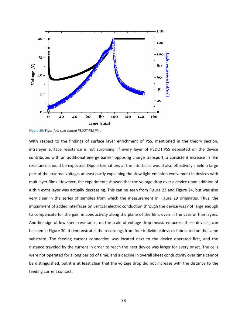
Another sign of low sheet-resistance, on the scale of voltage drop measured across these devices, can
be seen in Figure 30. It demonstrates the recordings from four individual devices fabricated on the same
substrate. The feeding current connection was located next to the device operated first, and the
distance traveled by the current in order to reach the next device was larger for every onset. The cells
were not operated for a long period of time, and a decline in overall sheet conductivity over time cannot
be distinguished, but it is at least clear that the voltage drop did not increase with the distance to the
feeding current contact.
34
Figure 30: Four devices fabricated on one substrate. Every device is operated separately, in a consecutive sequence.
The trend of enhanced light emission for intermediate number of PEDOT:PSS layers is not fully
understood. A tentative explanation is based on the possible chemical interactions between the
PEDOT:PSS electrode and the active material layer, enhanced by insufficient drying. Complete drying of
a very thick film might be difficult to accomplish, and it is possible that the multilayer procedure of
sequential depositing and curing resulted in films with significantly lower water content. The presence
of water in PEDOT:PSS is, in addition to impairing conduction, thought to enhance the exchange of
cations between the PEDOT:PSS film and its surroundings. As was remarked in the theory section,
migration of sodium ions across the glass substrate/PEDOT:PSS interface has been reported together
with suggested chemical interactions of sodium ions and the PEDOT:PSS complex [32]. This is of
importance as the PEDOT:PSS film was spin coated on a glass substrate. Spin coating and annealing of
one thin layer at a time should impose layers of alternated PEDOT and PSS enriched material,
respectively, as the concentration of PSS is observed to be higher in the surface region of a single film
[28]. The concentration of protons is low in areas of low PSS excess, thus detaining the ion exchange
rate and reducing the diffusion depth. Also, potassium ions are present in the active material blend and
could diffuse into the PEDOT:PSS film upon deposition. Potassium behaves chemically similarly to
sodium, and similar reactions are conceivable. Further, such ion exchange would imply proton migration
into the active layer, in order to maintain electroneutrality. The influence of such intrusion is not known.
The active material is very sensitive to humidity when the device is operating, and if water is fed to it
from the PEDOT:PSS, fast degeneration would occur. This explanation is in accordance with the low
35
performance of multilayer PEDOT:PSS devices, spin coated with short time intervals, as the mean time
drying was diminished.
5.2.3 PEDOT:PSS on top
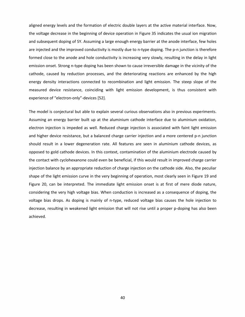
As fabrication of an LEC of coaxial geometry
requires a transparent outer electrode, the
order of deposition was reversed, as shown in
Figure 31. The metal electrode was now on
bottom, and metal penetration through the
active layer during fabrication was no longer
an issue. Devices were fabricated with
aluminium or gold electrodes. As PEDOT:PSS
was now deposited after the active material,
the device had to be transferred from the
inert glove box atmosphere out in ambient conditions. The PEDOT:PSS layer was spin coated at (1: 700
rpm, 700 rpm/sec, 50 sec, 2: 1500 rpm, 700rpm/sec, 10 sec). As the usually high temperature annealing
would have caused damage to the active material, the samples were transferred back into nitrogen
atmosphere following PEDOT:PSS deposition and dried on a hotplate at 323 K. The annealing time was
not less than 36 h. During this period of time, technical problems arose with the measurement
equipment that obstructed data saving and processing. Also, the compliance voltage could not be set to
a higher value than 15 V.
Three devices were fabricated on the same substrate via the evaporation of the aluminium electrodes.
During measurements the aluminium electrode was biased negatively. The positive electrode, in this
case the PEDOT:PSS film, covered the entire area of the substrate, and the external probe connection
was fixed to the same point throughout the measurements of all devices on the substrate.
Consequentially, current must pass along the sheet of the film in order to reach the device under test,
and the distance varies between the devices. Due to failure of the measurement equipment light
emission could not be recorded for the first device, closest to the positive probe connection. Compared
to previous results obtained for devices with PEDOT:PSS on bottom, performance appeared good and
light emission was rather uniform from the entire device area. Compliance voltage was not reached
during the light emission development towards and past its maximum, and the voltage was slowly
increasing from its minimum value at about 6.5 V. Compliance voltage was hit after more than six hours
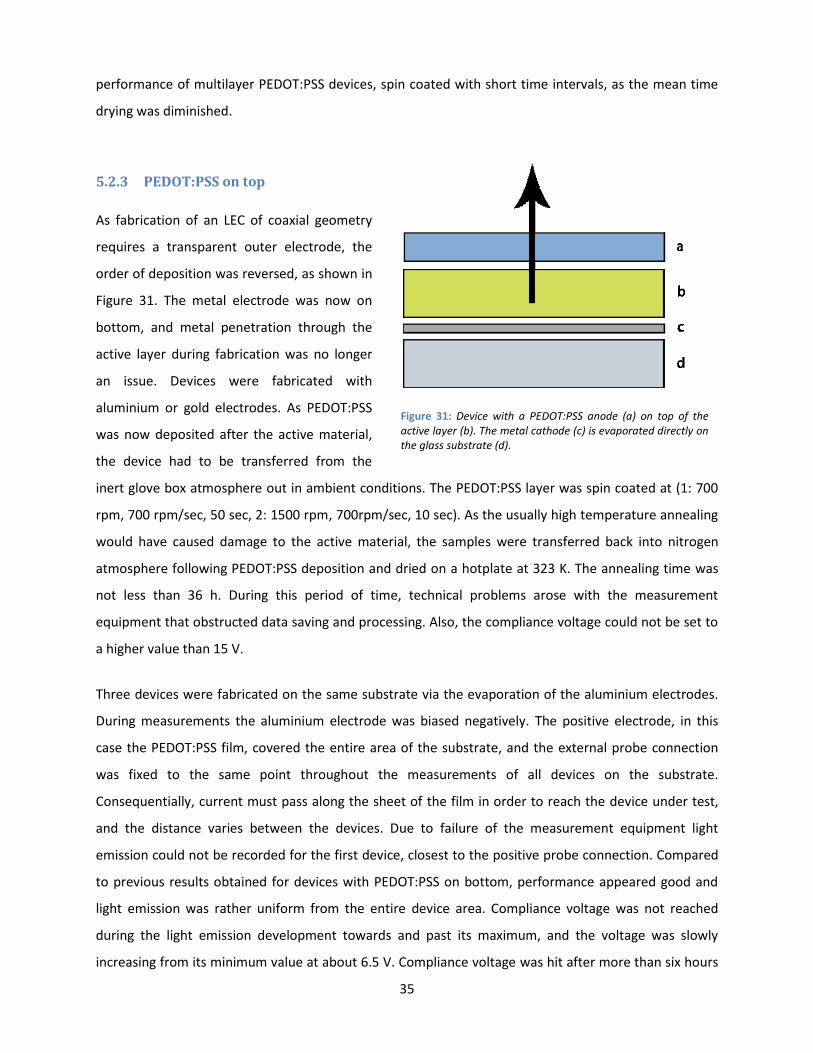
Figure 31: Device with a PEDOT:PSS anode (a) on top of the active layer (b). The metal cathode (c) is evaporated directly on the glass substrate (d).
36
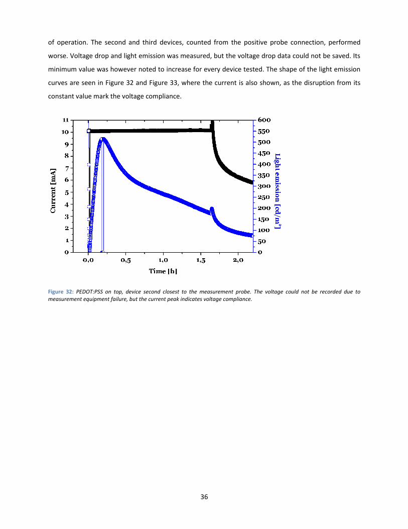
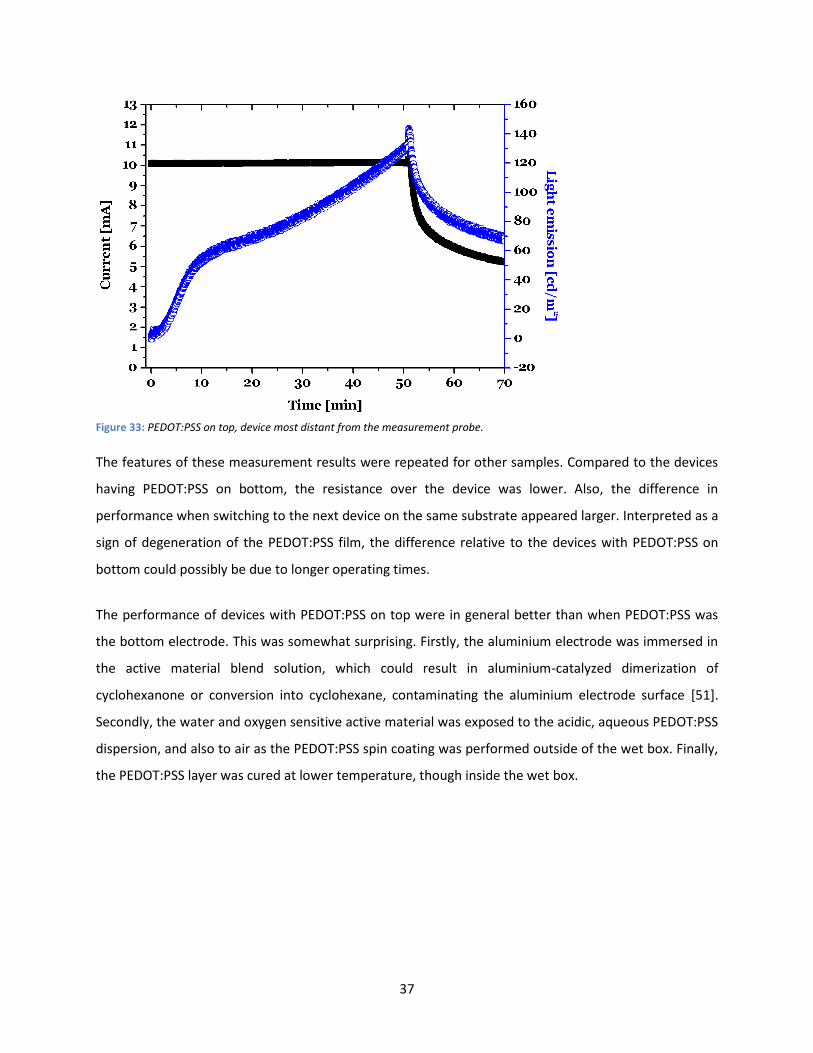
of operation. The second and third devices, counted from the positive probe connection, performed
worse. Voltage drop and light emission was measured, but the voltage drop data could not be saved. Its
minimum value was however noted to increase for every device tested. The shape of the light emission
curves are seen in Figure 32 and Figure 33, where the current is also shown, as the disruption from its
constant value mark the voltage compliance.
Figure 32: PEDOT:PSS on top, device second closest to the measurement probe. The voltage could not be recorded due to measurement equipment failure, but the current peak indicates voltage compliance.
37
Figure 33: PEDOT:PSS on top, device most distant from the measurement probe.
The features of these measurement results were repeated for other samples. Compared to the devices
having PEDOT:PSS on bottom, the resistance over the device was lower. Also, the difference in
performance when switching to the next device on the same substrate appeared larger. Interpreted as a
sign of degeneration of the PEDOT:PSS film, the difference relative to the devices with PEDOT:PSS on
bottom could possibly be due to longer operating times.
The performance of devices with PEDOT:PSS on top were in general better than when PEDOT:PSS was
the bottom electrode. This was somewhat surprising. Firstly, the aluminium electrode was immersed in
the active material blend solution, which could result in aluminium-catalyzed dimerization of
cyclohexanone or conversion into cyclohexane, contaminating the aluminium electrode surface [51].
Secondly, the water and oxygen sensitive active material was exposed to the acidic, aqueous PEDOT:PSS
dispersion, and also to air as the PEDOT:PSS spin coating was performed outside of the wet box. Finally,
the PEDOT:PSS layer was cured at lower temperature, though inside the wet box.
38
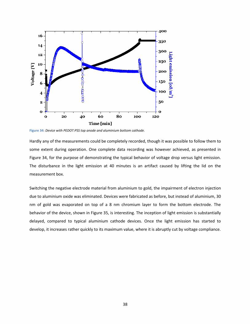
Figure 34: Device with PEDOT:PSS top anode and aluminium bottom cathode.
Hardly any of the measurements could be completely recorded, though it was possible to follow them to
some extent during operation. One complete data recording was however achieved, as presented in
Figure 34, for the purpose of demonstrating the typical behavior of voltage drop versus light emission.
The disturbance in the light emission at 40 minutes is an artifact caused by lifting the lid on the
measurement box.
Switching the negative electrode material from aluminium to gold, the impairment of electron injection
due to aluminium oxide was eliminated. Devices were fabricated as before, but instead of aluminium, 30
nm of gold was evaporated on top of a 8 nm chromium layer to form the bottom electrode. The
behavior of the device, shown in Figure 35, is interesting. The inception of light emission is substantially
delayed, compared to typical aluminium cathode devices. Once the light emission has started to
develop, it increases rather quickly to its maximum value, where it is abruptly cut by voltage compliance.
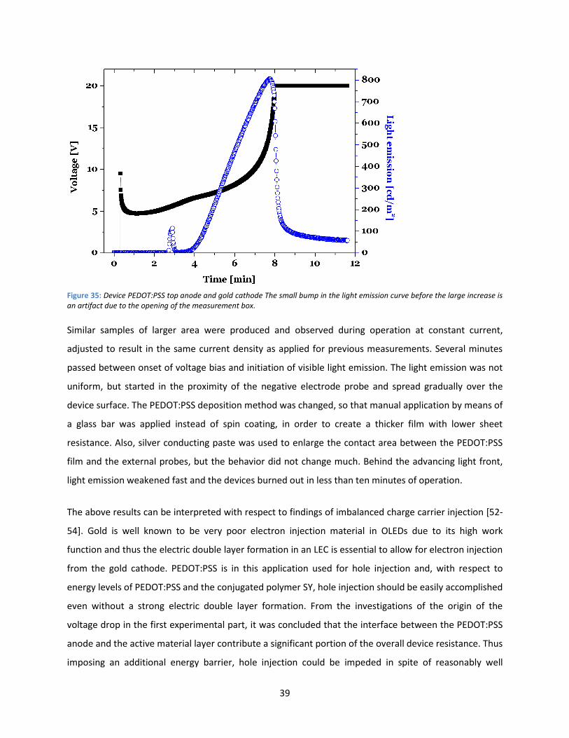
39
Figure 35: Device PEDOT:PSS top anode and gold cathode The small bump in the light emission curve before the large increase is an artifact due to the opening of the measurement box.
Similar samples of larger area were produced and observed during operation at constant current,
adjusted to result in the same current density as applied for previous measurements. Several minutes
passed between onset of voltage bias and initiation of visible light emission. The light emission was not
uniform, but started in the proximity of the negative electrode probe and spread gradually over the
device surface. The PEDOT:PSS deposition method was changed, so that manual application by means of
a glass bar was applied instead of spin coating, in order to create a thicker film with lower sheet
resistance. Also, silver conducting paste was used to enlarge the contact area between the PEDOT:PSS
film and the external probes, but the behavior did not change much. Behind the advancing light front,
light emission weakened fast and the devices burned out in less than ten minutes of operation.
The above results can be interpreted with respect to findings of imbalanced charge carrier injection [52-
54]. Gold is well known to be very poor electron injection material in OLEDs due to its high work
function and thus the electric double layer formation in an LEC is essential to allow for electron injection
from the gold cathode. PEDOT:PSS is in this application used for hole injection and, with respect to
energy levels of PEDOT:PSS and the conjugated polymer SY, hole injection should be easily accomplished
even without a strong electric double layer formation. From the investigations of the origin of the
voltage drop in the first experimental part, it was concluded that the interface between the PEDOT:PSS
anode and the active material layer contribute a significant portion of the overall device resistance. Thus
imposing an additional energy barrier, hole injection could be impeded in spite of reasonably well
40
aligned energy levels and the formation of electric double layers at the active material interface. Now,
the voltage decrease in the beginning of device operation in Figure 35 indicates the usual ion migration
and subsequent doping of SY. Assuming a large enough energy barrier at the anode interface, few holes
are injected and the improved conductivity is mostly due to n-type doping. The p-n junction is therefore
formed close to the anode and hole conductivity is increasing very slowly, resulting in the delay in light
emission onset. Strong n-type doping has been shown to cause irreversible damage in the vicinity of the
cathode, caused by reduction processes, and the deteriorating reactions are enhanced by the high
energy density interactions connected to recombination and light emission. The steep slope of the
measured device resistance, coinciding with light emission development, is thus consistent with
experience of “electron-only”-devices [52].
The model is conjectural but able to explain several curious observations also in previous experiments.
Assuming an energy barrier built up at the aluminium cathode interface due to aluminium oxidation,
electron injection is impeded as well. Reduced charge injection is associated with faint light emission
and higher device resistance, but a balanced charge carrier injection and a more centered p-n junction
should result in a lower degeneration rate. All features are seen in aluminium cathode devices, as
opposed to gold cathode devices. In this context, contamination of the aluminium electrode caused by
the contact with cyclohexanone could even be beneficial, if this would result in improved charge carrier
injection balance by an appropriate reduction of charge injection on the cathode side. Also, the peculiar
shape of the light emission curve in the very beginning of operation, most clearly seen in Figure 19 and
Figure 20, can be interpreted. The immediate light emission onset is at first of mere diode nature,
considering the very high voltage bias. When conduction is increased as a consequence of doping, the
voltage bias drops. As doping is mainly of n-type, reduced voltage bias causes the hole injection to
decrease, resulting in weakened light emission that will not rise until a proper p-doping has also been
achieved.
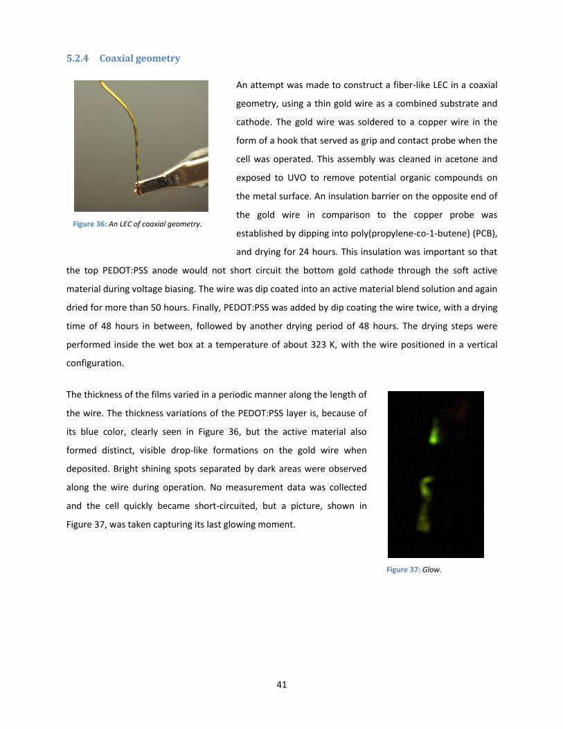
41
5.2.4 Coaxial geometry
An attempt was made to construct a fiber-like LEC in a coaxial
geometry, using a thin gold wire as a combined substrate and
cathode. The gold wire was soldered to a copper wire in the
form of a hook that served as grip and contact probe when the
cell was operated. This assembly was cleaned in acetone and
exposed to UVO to remove potential organic compounds on
the metal surface. An insulation barrier on the opposite end of
the gold wire in comparison to the copper probe was
established by dipping into poly(propylene-co-1-butene) (PCB),
and drying for 24 hours. This insulation was important so that
the top PEDOT:PSS anode would not short circuit the bottom gold cathode through the soft active
material during voltage biasing. The wire was dip coated into an active material blend solution and again
dried for more than 50 hours. Finally, PEDOT:PSS was added by dip coating the wire twice, with a drying
time of 48 hours in between, followed by another drying period of 48 hours. The drying steps were
performed inside the wet box at a temperature of about 323 K, with the wire positioned in a vertical
configuration.
The thickness of the films varied in a periodic manner along the length of
the wire. The thickness variations of the PEDOT:PSS layer is, because of
its blue color, clearly seen in Figure 36, but the active material also
formed distinct, visible drop-like formations on the gold wire when
deposited. Bright shining spots separated by dark areas were observed
along the wire during operation. No measurement data was collected
and the cell quickly became short-circuited, but a picture, shown in
Figure 37, was taken capturing its last glowing moment.
Figure 36: An LEC of coaxial geometry.
Figure 37: Glow.
42
6 Conclusions
It is shown possible to construct an LEC with PEDOT:PSS as the sole anode material, allowing for a light
emission exceeding 800 cd/m2 at an efficiency of 0.96 cd/A. Simple depositing methods are applied that
do not permit minute control of layer thickness and yet uniform light emission is demonstrated. The last
experiment shows that a geometry different from the flat cells previously produced is realizable. It is
concluded that the interface between PEDOT:PSS and the active layer accounts for a substantial part of
the device resistance. The order of deposition of the layers comprising the LEC is seen to be manifested
in device performance, probably due to interfacial phenomena such as surface energies, but possibly
also due to ion exchange between the layers and even the glass substrate. It has further been
demonstrated that the choice of cathode metal is of significant importance for the operation of LEC
devices with a PEDOT:PSS anode, and a tentative model is proposed to explain the characteristics that
discriminates the device operation in the case of aluminium versus gold.

43
7 Outlook
The development of an efficient LEC with a transparent polymer electrode that can be applied from a
water based dispersion would allow for large flexibility in applications of complex geometries of pliable
character. Environmentally friendly production of devices would be possible in large scale and at a low
production cost. Further investigations should aim to deepen the understanding of the fundamental
physical and chemical processes governing the performance of such a device.
Starting with the material used in this thesis, the validity of the proposed explanation models should be
examined. By scanning Kelvin probe microscopy, the spatial location of device resistance could be
established. Surface treatments to systematically vary the energy barrier for both holes and electron
injection would reveal if charge injection balancing would increase device performance. Different
methods have been presented, such as argon sputtering and treatment with HCl-methanol solution, for
the purpose of etching away the PSS enriched, poorly conducting surface layer [55-57]. Tests could also
be performed on devices with gold electrodes, coated with a suitably isolating layer for reducing
electron injection. Different substrates could be used for investigation of the influence of the substrate
material on PEDOT:PSS and methods for preventing intralayer ion migration could be examined. If ion
leakage from the active material is strong enough to cause dedoping, some effects are anticipated if the
electrolyte concentration is increased.
The quality of devices produced by dip coating can be improved by tuning variables such as viscosity of
the solutions and surface treatments.
44
8 Bibliography
1. Gao, Y., Surface analytical studies of interfaces in organic semiconductor devices. Materials Science and Engineering: R: Reports, 2010. 68(3): p. 39-87.
2. Chen, X.-W., W.C.H. Choy, and S. He, Efficient and Rigorous Modeling of Light Emission in Planar Multilayer Organic Light-Emitting Diodes. J. Display Technol., 2007. 3(2): p. 110-117.
3. Matyba, P., et al., The dynamic organic p–n junction. Nature Materials, 2009. 8(8): p. 672-676.
4. van Reenen, S., et al., A Unifying Model for the Operation of Light-Emitting Electrochemical Cells. Journal of the American Chemical Society, 2010. 132(39): p. 13776-13781.
5. Matyba, P., et al., Graphene and Mobile Ions: The Key to All-Plastic, Solution-Processed Light-Emitting Devices. ACS Nano, 2010. 4(2): p. 637-642.
6. Robinson, N.D., et al., Electrochemical doping during light emission in polymer light-emitting electrochemical cells. Physical Review B, 2008. 78(24): p. 245202.
7. Gao, J. and J. Dane, Visualization of electrochemical doping and light-emitting junction formation in conjugated polymer films. Applied Physics Letters, 2004. 84(15): p. 2778-2780.
8. Pei, Q. and A.J. Heeger, Operating mechanism of light-emitting electrochemical cells. Nat Mater, 2008. 7(3): p. 167-167.
9. deMello, J.C., et al., Ionic space-charge effects in polymer light-emitting diodes. Physical Review B, 1998. 57(20): p. 12951.
10. deMello, J.C., et al., Electric Field Distribution in Polymer Light-Emitting Electrochemical Cells. Physical Review Letters, 2000. 85(2): p. 421.
11. deMello, J.C., Interfacial feedback dynamics in polymer light-emitting electrochemical cells. Physical Review B, 2002. 66(23): p. 235210.
12. Slinker, J.D., et al., Direct measurement of the electric-field distribution in a light-emitting electrochemical cell. Nat Mater, 2007. 6(11): p. 894-899.
13. Malliaras, G.G., et al., Operating mechanism of light-emitting electrochemical cells. Nat Mater, 2008. 7(3): p. 168-168.
14. Moliton, A. and R.C. Hiorns, Review of electronic and optical properties of semiconducting π-conjugated polymers: applications in optoelectronics. Polymer International, 2004. 53(10): p. 1397-1412.
15. - - , Electronic Evolution of Poly(3,4-ethylenedioxythiophene) (PEDOT): From the Isolated Chain to the Pristine and Heavily Doped Crystals. Journal of the American Chemical Society, 2008. 130(50): p. 16880-16889.
45
16. Bässler, H., Charge Transport in Disordered Organic Photoconductors a Monte Carlo Simulation Study. physica status solidi (b), 1993. 175(1): p. 15-56.
17. Wallace, G.G., et al., Conductive Electroactive Polymers: Intelligent Polymer Systems, in Conductive Electroactive Polymers: Intelligent Polymer Systems. 2008, CRC Press: Boca Raton.
18. MacDiarmid, A.G. and A.J. Epstein, Secondary doping in polyaniline. Synthetic Metals, 1995. 69(1-3): p. 85-92.
19. Hoven, C.V., et al., Chemically fixed p-n heterojunctions for polymer electronics by means of covalent B-F bond formation. Nat Mater, 2010. 9(3): p. 249-252.
20. Lonergan, M.C., et al., Electrochemical Characterization of Polyacetylene Ionomers and Polyelectrolyte-Mediated Electrochemistry toward Interfaces between Dissimilarly Doped Conjugated Polymers. Journal of the American Chemical Society, 2002. 124(4): p. 690-701.
21. Matyba, P., M.R. Andersson, and L. Edman, On the desired properties of a conjugated polymer-electrolyte blend in a light-emitting electrochemical cell. Organic Electronics, 2008. 9(5): p. 699-710.
22. m, A., et al., Separating Ion and Electron Transport: The Bilayer Light-Emitting Electrochemical Cell. Journal of the American Chemical Society, 2010. 132(19): p. 6646-6647.
23. Kirchmeyer, S. and K. Reuter, Scientific importance, properties and growing applications of poly(3,4-ethylenedioxythiophene). Journal of Materials Chemistry, 2005. 15(21): p. 2077-2088.
24. Huang, J., et al., Influence of thermal treatment on the conductivity and morphology of PEDOT/PSS films. Synthetic Metals, 2003. 139(3): p. 569-572.
25. Huang, J., et al., Investigation of the Effects of Doping and Post-Deposition Treatments on the Conductivity, Morphology, and Work Function of Poly(3,4-ethylenedioxythiophene)/Poly(styrene sulfonate) Films. Advanced Functional Materials, 2005. 15(2): p. 290-296.
26. Jönsson, S.K.M., et al., The effects of solvents on the morphology and sheet resistance in poly(3,4-ethylenedioxythiophene)-polystyrenesulfonic acid (PEDOT-PSS) films. Synthetic Metals, 2003. 139(1): p. 1-10.
27. Nardes, A.M., M. Kemerink, and R.A.J. Janssen, Anisotropic hopping conduction in spin-coated PEDOT:PSS thin films. Physical Review B, 2007. 76(8): p. 085208.
28. Nardes, A.M., et al., Microscopic Understanding of the Anisotropic Conductivity of PEDOT:PSS Thin Films. Advanced Materials, 2007. 19(9): p. 1196-1200.
29. Ionescu-Zanetti, C., et al., Semiconductive Polymer Blends: Correlating Structure with Transport Properties at the Nanoscale. Advanced Materials, 2004. 16(5): p. 385-389.
30. Peisert, H., et al., The interface between phthalocyanines and PEDOT:PSS: evidence for charge transfer and doping. Surface Science, 2004. 566-568(Part 1): p. 554-559.
46
31. Tengstedt, C., et al., Fermi-level pinning at conjugated polymer interfaces. Applied Physics Letters, 2006. 88(5): p. 053502-3.
32. Crispin, X., et al., Conductivity, morphology, interfacial chemistry, and stability of poly(3,4-ethylene dioxythiophene)–poly(styrene sulfonate): A photoelectron spectroscopy study. Journal of Polymer Science Part B: Polymer Physics, 2003. 41(21): p. 2561-2583.
33. Sakamoto, S., et al., Raman spectral changes of PEDOT-PSS in polymer light-emitting diodes upon operation. Chemical Physics Letters, 2005. 412(4-6): p. 395-398.
34. de Kok, M.M., et al., Modification of PEDOT:PSS as hole injection layer in polymer LEDs. physica status solidi (a), 2004. 201(6): p. 1342-1359.
35. Lapkowski, M. and A. Pron, Electrochemical oxidation of poly(3,4-ethylenedioxythiophene) -- "in situ" conductivity and spectroscopic investigations. Synthetic Metals, 2000. 110(1): p. 79-83.
36. Salsamendi, M., et al., Synthesis and electro-optical characterization of new conducting PEDOT/Au-nanorods nanocomposites. Polymers for Advanced Technologies, 2010: p. n/a-n/a.
37. Chen, Y., et al., Enhanced optical and electrical properties of PEDOT: PSS films by the addition of MWCNT-sorbitol. Synthetic Metals, 2009. 159(17-18): p. 1701-1704.
38. Gadisa, A., et al., Transparent polymer cathode for organic photovoltaic devices. Synthetic Metals, 2006. 156(16-17): p. 1102-1107.
39. Li, J., et al., Organic Light-Emitting Diodes Having Carbon Nanotube Anodes. Nano Letters, 2006. 6(11): p. 2472-2477.
40. Ouyang, J., et al., High-Conductivity Poly(3,4-ethylenedioxythiophene):Poly(styrene sulfonate) Film and Its Application in Polymer Optoelectronic Devices. Advanced Functional Materials, 2005. 15(2): p. 203-208.
41. Harkema, S., et al. Large area ITO-free flexible white OLEDs with Orgacon PEDOT:PSS and printed metal shunting lines. 2009. San Diego, CA, USA: SPIE.
42. Sandstrom, A., P. Matyba, and L. Edman, Yellow-green light-emitting electrochemical cells with long lifetime and high efficiency. Applied Physics Letters, 2010. 96(5): p. 053303-3.
43. Fang, J., P. Matyba, and L. Edman, The Design and Realization of Flexible, Long-Lived Light-Emitting Electrochemical Cells. Advanced Functional Materials, 2009. 19(16): p. 2671-2676.
44. Uddin, M., et al., Effect of spin coating on the curing rate of epoxy adhesive for the fabrication of a polymer optical waveguide. Journal of Electronic Materials, 2004. 33(3): p. 224-228.
45. Heriot, S.Y. and R.A.L. Jones, An interfacial instability in a transient wetting layer leads to lateral phase separation in thin spin-cast polymer-blend films. Nat Mater, 2005. 4(10): p. 782-786.
46. Li, X., Y. Han, and L. An, Surface Morphology Evolution of Thin Triblock Copolymer Films during Spin Coating. Langmuir, 2002. 18(13): p. 5293-5298.
47
47. Gerlach, A., et al., In-situ X-ray scattering studies of OFET interfaces. physica status solidi (a), 2008. 205(3): p. 461-474.
48. Lightfoot, P., M.A. Mehta, and P.G. Bruce, Crystal Structure of the Polymer Electrolyte Poly(ethylene oxide)3:LiCF3SO3. Science, 1993. 262(5135): p. 883-885.
49. Croce, F., et al., Physical and Chemical Properties of Nanocomposite Polymer Electrolytes. The Journal of Physical Chemistry B, 1999. 103(48): p. 10632-10638.
50. He, Y., B. Zhu, and Y. Inoue, Hydrogen bonds in polymer blends. Progress in Polymer Science, 2004. 29(10): p. 1021-1051.
51. Ganguly, P., Reactions of ketones on oxide surfaces. I. Reaction sequence of cyclohexanone on alumina. Proceedings Mathematical Sciences, 1977. 86(1): p. 65-79.
52. Dane, J. and J. Gao, Imaging the degradation of polymer light-emitting devices. Applied Physics Letters, 2004. 85(17): p. 3905-3907.
53. Tang, S. and L. Edman, Quest for an Appropriate Electrolyte for High-Performance Light-Emitting Electrochemical Cells. The Journal of Physical Chemistry Letters, 2010. 1(18): p. 2727-2732.
54. Shin, J.H., et al., Polymer Light-Emitting Electrochemical Cells: Doping Concentration, Emission-Zone Position, and Turn-On Time. Adv. Funct. Mater., 2007. 17(11): p. 1807-1813.
55. Hwang, J., F. Amy, and A. Kahn, Spectroscopic study on sputtered PEDOT · PSS: Role of surface PSS layer. Organic Electronics, 2006. 7(5): p. 387-396.
56. Kang, K.S., et al., Conductivity enhancement of conjugated polymer after HCl-methanol treatment. Thin Solid Films, 2009. 517(20): p. 5909-5912.
57. Kislyuk, V.V. and et al., Interfacial properties and formation of a Schottky barrier at the CdS/PEDOT : PSS hybrid junction. Journal of Physics D: Applied Physics, 2010. 43(18): p. 185301.