Embed Size (px)
Citation preview

DEVELOPMENT OF EDA TECHNIQUES FOR
POWER MODULE EMI MODELING AND LAYOUT
OPTIMIZATIONTRISTAN EVANS, QUANG LE, BALAJI NARAYANASAMY, YARUI PENG, FANG LUO, H. ALAN MANTOOTH
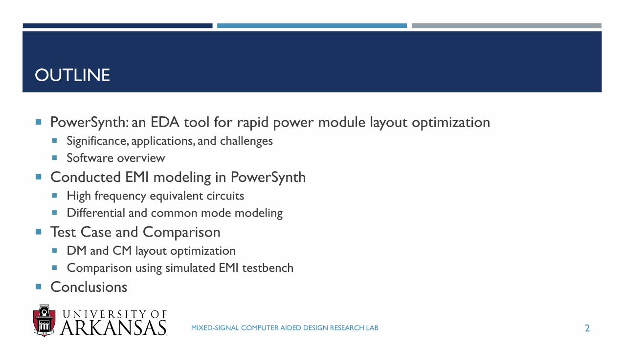
OUTLINE
PowerSynth: an EDA tool for rapid power module layout optimization Significance, applications, and challenges
Software overview
Conducted EMI modeling in PowerSynth High frequency equivalent circuits
Differential and common mode modeling
Test Case and Comparison DM and CM layout optimization
Comparison using simulated EMI testbench
Conclusions
MIXED-SIGNAL COMPUTER AIDED DESIGN RESEARCH LAB 2

POWERSYNTH
3

MULTICHIP POWER MODULES (MCPM)
• Renewable energy• Electric vehicles and traction• Aerospace• Industry
Applications
• Integration of power and control circuitry
• Increased power densityAdvantages
• Multidomain: electrical, thermal, mechanical
• Integration and EMC• Design iteration
Challenges
MIXED-SIGNAL COMPUTER AIDED DESIGN RESEARCH LAB 4
R&D 100 Award-Winning MCPM Design
by UA and APEI

STATE OF THE ART AND CHALLENGES
MIXED-SIGNAL COMPUTER AIDED DESIGN RESEARCH LAB 5
▪ Common Methodologies
▪ Finite Element Analysis (FEA)
▪ Circuit Simulation
▪ Advantages
▪ Increased accuracy for finer meshes
▪ CAD import, data and image export
▪ Long simulation times
▪ To solve closed form higher order differential equations
▪ To build finer mesh
▪ To analyze all parameters on finer mesh
▪ Single solution at a time
▪ User attention/input required (to modify/optimize
geometry/mesh if one option doesn’t work)
Commercial Solutions
▪ Tools used to simulate
electrical/thermal/mechanical/EMI
▪ ICEPAK
▪ Q3D
▪ HFSS
▪ COMSOL
▪ SolidWorks
▪ MATLAB &
Simulink
▪ FastHenry
Challenges
No full verification flow for
power electronics exists

SOLUTION: POWERSYNTH
MIXED-SIGNAL COMPUTER AIDED DESIGN RESEARCH LAB 6
Symbolic
Layout/ Netlist
Performance
Criteria
Device & Layer
Materials &
Dimensions
Multi-Objective
Optimization
Layout
Solution
Set
Export
SolutionFixed
constraints/
Design rules
Model
Multi-objective optimization tool for MCPM design
Reduced order electrical and thermal
models ⇒ Fast evaluation in
optimization loop

POWERSYNTH: OVERVIEW
MIXED-SIGNAL COMPUTER AIDED DESIGN RESEARCH LAB 7
Workflow Diagram Component Selection
Post-Optimization
Analysis

MCPM PHYSICAL DESCRIPTION AND
COMPONENT SELECTION
MIXED-SIGNAL COMPUTER AIDED DESIGN RESEARCH LAB 8
Physical Layout
Symbolic Layout
Trace Trace
Substrate
Metal
Baseplate
0.22
0.41
0.64
0.41
6.0
Min spacing
1.2
Min width
1.2
Min enclosure
0.2Device
Thickness
Layer Stack and Materials
MDK and Constraints
MOSFET
SBD
Terminals and Leads
Component Selection

OPTIMIZATION
MIXED-SIGNAL COMPUTER AIDED DESIGN RESEARCH LAB 9
• Four different optimization algorithms are available:
• Non-guided randomization : Built-in solution generator
• Evolutionary approach: NSGAII
• Gradient-based approach: Weighted Sum Method
• Stochastic approach: Simulated Annealing
• Performance metrics for optimization:
• Electrical parasitics
• Device temperature
DC+
DC-
M1
M3
High
Low
Out
M2
M4
Power loop and heat sourcesConducted EMI now a cost function
For more information on models:T. M. Evans et al., "PowerSynth: A Power Module Layout Generation Tool," in IEEE Transactions on Power
Electronics, vol. 34, no. 6, pp. 5063-5078, June 2019. doi: 10.1109/TPEL.2018.2870346

MULTI-OBJECTIVE SOLUTION BROWSER
MIXED-SIGNAL COMPUTER AIDED DESIGN RESEARCH LAB 10
View and sort through performance trade-off data
Select solution which best suits design problem
Supports 2D and 3D data visualization
An envelope or window is used to sort through high dimensional data
Browser for selecting layout solutions from a Pareto front with the options to save and export

DESIGN EXPORT
MIXED-SIGNAL COMPUTER AIDED DESIGN RESEARCH LAB 11
Export to SolidWorks or Q3D
Further electrical and thermal verification through Q3D and SolidWorks
Export for manufacturing from SolidWorks
Export to simulated EMI testbench
Export electrical parasitics netlist for circuit simulation
SolidWorks
ANSYS Q3D
Parasitics Netlist

CONDUCTED EMI MODELING
12

EMI IN POWER ELECTRONICS
EMI can be radiated or conducted with several coupling paths
Several standards exist for EMC based on application and region
Conducted noise paths: Common mode (CM) noise
between power circuit and ground
Differential mode (DM) noise follows same path as power delivery
Separating CM and DM Accomplished with noise
separator Simplifies filter design Aids in troubleshooting
MIXED-SIGNAL COMPUTER AIDED DESIGN RESEARCH LAB 13
Source Victim
Radiative
Capacitive
Inductive
Conductive
Power
SourceEUT
Power
Lines
Common
Ground
Differential
Mode Path
Common
Mode Path
Noise Propagation
Mechanisms
Conducted Noise
Paths
How does power module layout
affect conducted EMI?

HIGH FREQUENCY EQUIVALENT CIRCUITS
MIXED-SIGNAL COMPUTER AIDED DESIGN RESEARCH LAB 14
DM: TOTAL Loop Inductance & Coss Resonance
CM: Trace Capacitance to Ground
Q. Liu, Modular Approach for Characterizing and Modeling Conducted EMI
Emissions in Power Converters, Doctoral Dissertation, Virginia Tech, 2005.
Converter System Overview DM Equivalent Circuit CM Equivalent Circuit
𝑉𝐷𝑀 =𝑉𝐿𝐼𝑆𝑁,1 − 𝑉𝐿𝐼𝑆𝑁,2
2𝑉𝐶𝑀 =
𝑉𝐿𝐼𝑆𝑁,1 + 𝑉𝐿𝐼𝑆𝑁,22
FD Current Source (DM) and Voltage Source (CM) as Excitation

COMMON MODE MODELING
L, R parasitics extracted using PowerSynth response surface model (RSM)
Parasitic capacitances calculated based on trace area and separation from ground
CM voltage gain transfer function employed in calculating CM noise
MIXED-SIGNAL COMPUTER AIDED DESIGN RESEARCH LAB 15
CM Equivalent Circuit Module Trace Capacitance
𝐶 =𝜖𝐴
𝑑
𝑉𝐶𝑀 = 𝑉𝐷𝑆𝐺𝐶𝑀
Trace Capacitance:
Common Mode Voltage:

CONDUCTED EMI TEST CASE AND SIMULATION
16

POWERSYNTH LAYOUT OPTIMIZATION
Loop inductance (layout only) used as surrogate for DM noise
CM noise calculated using modified nodal analysis (MNA) on HF equivalent circuit
Frequencies sampled geometrically between 10 kHz and 100 MHz
Average of CM voltage gain transfer function used in cost function
2201 layouts evaluated in 3675 s (228 shown)
MIXED-SIGNAL COMPUTER AIDED DESIGN RESEARCH LAB 17

SIMULATED EMI TEST BENCH
Automated export of PowerSynth design solutions
to commercial FEA EM solver
3D EM simulation results exported as S-parameter
model for circuit simulation
Circuit simulation includes total system including
detailed device models
Transient simulations with FFT analysis of results
possible
MIXED-SIGNAL COMPUTER AIDED DESIGN RESEARCH LAB 18
Circuit Setup Used:
• Half bridge power module, double pulse test
• Single SiC device / switch pos.
• 10 A, 600 V DC Bus
• 25 kHz switching, 50% duty cycle

CM RESULTS COMPARISON
MIXED-SIGNAL COMPUTER AIDED DESIGN RESEARCH LAB 19
PowerSynth correctly identifies trend in CM
noise genereation

DM RESULTS COMPARISON
MIXED-SIGNAL COMPUTER AIDED DESIGN RESEARCH LAB 20
DM results not as profound,
but PowerSynth prediction
still follows simulated trends

CONCLUSIONS
EDA techniques for power electronic modules show promise for reducing design iterations
Moving toward performance-based optimization instead of simply pure analytics (EMI reduction instead of blind
parasitics reduction)
Moving forward:
Optimize for signal integrity in gate loop toward preventing false turn on and improving current sharing
Explore layout impacts on radiated EMI
Test and validate with physical measurements
MIXED-SIGNAL COMPUTER AIDED DESIGN RESEARCH LAB 21