Embed Size (px)
Citation preview

DEVELOPMENT OF DETECTION AND FREQUENCY
MEASUREMENT CIRCUIT FOR PENNING ION TRAP
By
ASHIF REZA
(Enrollment No: ENGG04201104004)
VARIABLE ENERGY CYCLOTRON CENTRE
Kolkata-700064, India
A thesis submitted to the
Board of Studies in Engineering Sciences
In partial fulfillment of requirements
for the Degree of
DOCTOR OF PHILOSOPHY
of
HOMI BHABHA NATIONAL INSTITUTE
May, 2017


i
STATEMENT BY AUTHOR
This dissertation has been submitted in partial fulfillment of requirements for an
advanced degree at Homi Bhabha National Institute (HBNI) and is deposited in the
Library to be made available to borrowers under rules of the HBNI.
Brief quotations from this dissertation are allowable without special permission,
provided that accurate acknowledgement of source is made. Requests for permission
for extended quotation from or reproduction of this manuscript in whole or in part
may be granted by the Competent Authority of HBNI when in his or her judgment the
proposed use of the material is in the interests of scholarship. In all other instances,
however, permission must be obtained from the author.
ASHIF REZA

ii
DECLARATION
I, hereby declare that the investigation presented in the thesis has been carried out by
me. The work is original and has not been submitted earlier as a whole or in part for a
degree / diploma at this or any other Institution / University.
ASHIF REZA
iii
List of Publications arising from the thesis
Journal Publications:-
1. Ashif Reza, Anuraag Misra, and Parnika Das, “An improved model to predict
bandwidth enhancement in an inductively tuned common source amplifier”, Rev. Sci.
Instrum., 87 (5), 054710, 2016.
2. Ashif Reza, A. K. Sikdar, P. Das, I. Chatterjee, and K. Banerjee, “Development of
low noise amplifier and associated RF switching circuit for the Penning ion trap,”
Indian Journal of Cryogenics, 41 (1), 146, 2016.
3. “Ashif Reza, Kumardeb Banerjee, Parnika Das, Kalyankumar Ray, Subhankar
Bandyopadhyay, and Bivas Dam, “An in situ trap capacitance measurement and ion-
trapping detection scheme for a Penning ion trap facility”, Rev. Sci. Instrum., 88 (3),
034705, 2017.
Conference Publications:-
1. P. Das, A. K. Sikdar, A. Reza, Subrata Saha, A. Dutta Gupta, S. K. Das, R. Guin, S.
Murali, A. Choudhury, A. Goswami, H. P. Sharma, A. De, A. Ray, “Development of
VECC Cryogenic Penning Ion Trap: A Report”, Proceedings of the DAE Symp. on
Nucl. Phys., 56, pp. 1082-1083, 2011.
2. P. Das, A. K. Sikdar, A. Reza, Subrata Saha, A. Dutta Gupta, S. K. Das, R. Guin, S.
Murali, A. Goswami, H. P. Sharma, A. De, K. Banerjee, B. Dam, A.Ray, “VECC
Cryogenic Penning Ion Trap: A status report,” in Proceedings of the DAE Symp. on Nucl.
Phys., 57, pp. 876-877, 2012.
3. A. Reza, A. K. Sikdar, P. Das, U. Bhunia, A. Mishra, K. Banerjee, B. Dam, A.Ray,
"Capacitance measurement of Penning trap electrode assembly at cryogenic
temperature", Proceedings of the DAE Symp. on Nucl. Phys., 58, pp. 878-879, 2013.

iv
4. A. Reza, A. K. Sikdar, P. Das, U. Bhunia, A. Misra, K. Banerjee, B. Dam, A.Ray,
“Trap Capacitance Measurement at cryogenic temperature,” Proceedings of the
National Symposium on Nuclear Instrumentation, 2013.
5. P. Das, A. K. Sikdar, A. Reza, Subrata Saha, A. Dutta Gupta, M. Ahammed, S. K.
Das, R. Guin, S. Murali, K. Banerjee, B. Dam, A.Ray, “Progress in VECC Cryogenic
Penning Ion Trap Development”, Proceedings of the DAE Symp. on Nucl. Phys., 58,
pp. 880-881, 2013.
6. A. K. Sikdar, A. Reza, S. K. Das, K. Banerjee, B. Dam, P. Das, A.Ray, “Progress in
VECC Cryogenic Penning Ion Trap Development”, Proceedings of the DAE Symp. on
Nucl. Phys., 59, pp. 904-905, 2014.
7. Ashif Reza, A.K. Sikdar, P. Das, I. Chatterjee, K. Banerjee, “Development of
cryogenic instrumentation for Penning ion trap”, Proceedings of 25th
National
Symposium on Cryogenics, 2014.
8. A. K. Sikdar, A. Reza, R. Menon, Y. P. Nabhiraj, K. Banerjee, B. Dam, P. Das, A.
Ray, “Progress in VECC Penning Ion Trap Development”, Proceedings of the DAE-
BRNS Symp. on Nucl. Phys., 60, pp. 926-927, 2015.
9. Ashif Reza, Anuraag Misra, Saikat Sarkar, Arindam Kumar Sikdar, Parnika Das,
"Development of a helical resonator for ion trap application", Proceedings of 2015
IEEE Applied Electromagnetics Conference, pp. 1 – 2, 2015.

v
10. Ashif Reza, Anuraag Misra, Indira Chatterjee, Parnika Das, "Development and
characterization of a high frequency low noise amplifier", Proceedings of Twenty
Second National Conference on Communications, 2016.
11. Ashif Reza, A.K. Sikdar, P. Das, “Design and characterization of a low noise
amplifier operating at cryogenic temperature”, Proceedings of 26th
National
Symposium on Cryogenics & Superconductivity, 2017.
Other Publications
Journal Publications:-
1. A.K. Sikdar, A. Ray, P. Das, A. Reza, “Design of a dynamically orthogonalized
Penning trap with higher order anharmonicity compensation”, Nucl. Instrum. Methods
Phys. Res. A., 712, 174, 2016.
Conference Publications:-
1. S. Dasgupta, A. Dutta, S. Bhattacharyya, P. Das, A. Reza, U. Bhuia, S. Saha, S.
Murali and M. H. Rashid, “Study of Field Profile of a Mini Orange Spectrometer
Magnet” , Proceedings of the DAE Symp. on Nucl. Phys., 57, pp. 950-951, 2012.
2. P. Das, R. Bogi, A. Reza, A. K. Sikdar, A. Nandi, “A Study on Uniformity of a
Magnet”, Proceedings of COMSOL conference, 2014.
ASHIF REZA

vi
Dedicated
to
my parents
Shri. MD Rezaul Haque
Smt. Zarina Sahnaj
and
my cute niece
Mysha

vii
ACKNOWLEDGEMENTS
First I would like to express my sincere gratitude to Dr. Parnika Das for her
excellent guidance, constant encouragement and support throughout the course of my
thesis work. Her continuous supervision and valuable discussions were extremely
helpful to complete my thesis work.
I would like to express my heartfelt thanks to Dr. Anuraag Misra for his
continuous cooperation, technical discussions and fruitful suggestions which he
offered from time to time. His wonderful approach towards a research problem was
very helpful to carry out my thesis work.
I would like to sincerely thanks to Dr. Kumardeb Banerjee (Professor, Jadavpur
University) for his valuable guidance and support during my thesis work. His broad
knowledge and understanding were very much important to complete my thesis work.
A special thank goes to Arindam Kumar Sikdar for his wonderful cooperation and
hard work which he provide during the installation of the experimental facility.
I tender my grateful thanks to Dr. Bivas Dam (Professor, Jadavpur University), Dr.
Pushpa M Rao (BARC, Mumbai), Dr. Sandip Pal, Dr. Paramita Mukherjee and Dr.
Anirban De for their support and helpful suggestions during my thesis work.
I would like to sincerely thank Dr. Amlan Ray (Ex-Head, Cryogenic Trap Section),
Dr. Sudhee Ranjan Banerjee (Ex-Head, Physics Group) and Shri Amitava Roy
(Director, VECC) for their continuous support to continue my work.
I express my sincere thanks to all the members of VECC, Kolkata for their support.
Last but not least, I owe my sincere thanks to God, my family and my friends for
giving me continuous support and encouragement during my life.

viii
CONTENTS
Page No.
Synopsis 1
List of Figures 11
List of Tables 17
List of Abbreviations 18
1. Introduction 19
1.1 Historical background 19
1.2 Motivation 19
1.3 Thesis contribution 22
2. Basics of Penning ion trap and detection schemes 25
2.1 History of ion trap 25
2.2 Penning ion trap 27
2.3 Equivalent electrical model of a charged particle in a Penning trap 32
2.4 Ion detection technique in a Penning ion trap 35
2.4.1 Broadband detection 35
2.4.2 Narrowband detection 37
2.5 Cryogenic Penning ion trap facility at VECC 41
2.5.1 Superconducting 5 Tesla magnet 41
2.5.2 Five electrode cylindrical Penning ion trap 43
2.6 Summary 44

ix
3. Design, implementation and characterization of a low noise amplifier 45
3.1 Introduction 45
3.2 Noise sources in a field effect transistor 48
3.3 Different amplifier topologies 50
3.4 Design of a low noise cascode amplifier 51
3.4.1 Circuit schematic and fabrication 52
3.4.2 Voltage gain measurement 53
3.4.3 Noise measurement 55
3.5 Design of a low noise inductively tuned common source amplifier 58
3.5.1 Improved model of a common source amplifier with inductive shunt
peaking 62
3.5.2 Circuit schematic and fabrication 66
3.5.3 Voltage gain measurement 68
3.5.4 Noise measurement 72
3.6 Inductively tuned common source LNA fabrication and testing 74
3.7 Cryogenic testing of LNA 75
3.8 Summary 81
4. Design and development of Colpitts oscillator for Penning ion trap 82
4.1 Introduction 82
4.2 Design and implementation of Colpitts oscillator module 86
4.2.1 Colpitts oscillator 86
4.2.2 Buffer amplifier 87
4.2.3 Low pass filter 88
4.3 Capacitance measurement scheme 91

x
4.4 Colpitts oscillator performance and test results 93
4.4.1 Amplitude and frequency stability 94
4.4.2 Accuracy and standard deviation 96
4.4.3 Sensitivity and resolution 99
4.4.4 Repeatability 99
4.4.5 Warm-up time 100
4.4.6 Response time 101
4.5 Measurement of trap capacitance 102
4.6 Trap capacitance measurement and trapped particle detection scheme 105
4.7 Summary 106
5. Design and study of a loaded helical resonator 107
5.1 Introduction 107
5.2 Quarter wave resonator 108
5.3 Quarter wave helical resonator 110
5.3.1 Design parameter 112
5.3.2 Effect of capacitive loading 113
5.3.3 Theoretical Design 115
5.4 HFSS simulation and fabrication 116
5.4.1 Simulation of capacitively loaded helical resonator 118
5.4.2 Fabrication and testing with different capacitive load 119
5.5 Summary 122
6. Trapping and detection of electrons in VECC Penning ion trap 123
6.1 Introduction 123
6.2 VECC Penning ion trap setup 124

xi
6.2.1 Magnetic field generation using permanent magnet 124
6.2.2 Five electrode flat endcap cylindrical Penning ion trap electrodes 125
6.2.3 Setup for generation of electrons 125
6.2.4 Cabling and assembly of Penning ion trap facility 127
6.2.5 Ultra high vacuum setup 129
6.3 Experimental testing and results 130
6.3.1 Performance test of the detection circuit without trapped electrons 131
6.3.2 Detection of trapped electrons at room temperature 133
6.3.3 Detection of trapped electrons at 100K 141
6.3.4 Testing of Colpitts oscillator to excite and detect the electrons 143
6.4 Summary 145
7. Conclusion and future outlook 146
7.1 Conclusion 146
7.2 Future prospect 149
Appendix
A. Constant current DC supply for thermionic generation of electrons 152
B. Measurement of trap capacitance at cryogenic temperature 156
C. Magnetic field generation using electromagnet 161
D. Design of a cryogenic RF switching and filtering circuit 163
Bibliography 165

1
Synopsis
Detection of signal and its estimation deal with the processing of signals to extract
the key information that they contain. The field of signal detection has been explored
continually due to its applications practically in every field. Detection of weak signal
is a challenging task as it is often contaminated by the presence of noise (such as the
inherent noise in the detection system and the interference due to the external
environment). A weak signal refers to a signal which has very low signal to noise ratio
(SNR). The key challenge in the detection of weak signal is to suppress noise and
extract the useful information from the signal. Recently weak signal detection has
become a topic of significant interest as it has great significance in radar,
communications, sonar, earthquake, industrial measurement, fault diagnosis besides
basic physics investigations.
A Low-Noise Amplifier (LNA) for detection of weak radio frequency (RF) signals
is a key component in weak signal detection and it is a leading area of research. Using
GaAs enhancement mode High-Electron Mobility FET devices as LNA is also gaining
importance for scientific applications in amplifying and detecting weak RF signals
under various conditions, including cryogenic temperatures, with the least possible
noise susceptibility. In RF region, it finds application in systems confined in RF
cavities at low temperatures as is encountered in several applications in physics,
physical chemistry and analytical chemistry. Nuclear magnetic resonance (NMR),
nuclear quadrupole resonance (NQR), electron paramagnetic resonance (EPR) and
microwave spectroscopy, Paul traps and Penning traps are typical examples of this.

2
One of the widely used scientific instruments for studying fundamental properties
of charged particles is a Penning ion trap. At Variable Energy Cyclotron Centre
(VECC), a Penning ion trap facility is being developed for high precision mass
measurement and beta-decay study. As per the design, a cylindrical Penning ion trap
assembly having five electrodes has been fabricated for trapping of electrons in 3-
dimension using the superposition of a quadrupolar DC field and a magnetic field. In
this facility, the trapped charged particles (electrons) will be detected through their
axial motion by observing the image currents on trap electrodes induced by the motion
of electrons. The image current developed on the trap electrodes are extremely feeble
(10 to 100 femto-amperes for single trapped particle) and detection of these weak
signals is a challenging task and requires a highly sensitive low noise detection circuit.
Based on the trap geometry and applied trapping potential, the axial oscillation
frequency of the trapped electrons is expected to be in the vicinity of 63 MHz.
The trapped particles oscillating in the axial direction within a Penning ion trap
can be electrically represented as a current source in parallel with the trap capacitance,
so it can be considered as a high impedance source. In order to detect the weak image
signal from such a high impedance source, a low noise amplifier with very high input
impedance is required so that the weak image signal transforms into a large voltage
signal at the input of amplifier. As the axial oscillation frequency for electron trapping
is ~ 63 MHz, the bandwidth of the amplifier must be sufficiently high to cover our
desired frequency zone of interest.
However, detection of very few numbers of trapped charged particles using only a
low noise amplifier is extremely difficult due to the effect of capacitive element that
reduces the effective impedance at high frequency and decreases the voltage signal

3
developed at the amplifier‟s input. In order to increase the detection sensitivity,
resonance based detection technique is widely employed where a high Q LC resonant
circuit (tank circuit) followed by a low noise amplifier is used to detect the weak
image signal. In order to design and implement the tank circuit, it is also required to
measure the capacitance of the Penning ion trap geometry.
The work reported in this thesis is aimed towards the indigenous development of
low noise detection circuit for image current detection application. As a part of the
detection scheme, a wide band low noise amplifier and a high Q tank circuit have been
developed indigenously at VECC. The capacitance of Penning ion trap assembly,
which is required for the design of the tank circuit, has been measured by direct
correlation of shift in oscillation frequency of a Colpitts oscillator.
The thesis is organized as follows: the historical background, research motivation
and contribution of the thesis are briefly discussed in Chapter-1.
Chapter-2 describes the fundamentals of a Penning ion trap and the various
detection schemes employed for the detection of weak image signal in a Penning ion
trap. The cryogenic Penning ion trap facility at VECC is also described in this chapter.
At VECC, a five electrode cylindrical Penning ion trap is being developed. In this
trap, it is planned to trap cloud of electrons and detect their axial motion by observing
the image charges on the trap electrodes induced by the motion of trapped electrons.
Various schemes can be used to detect this weak image signal. To detect this small
image current, a low noise amplifier with very high input impedance is required to get
a measurable voltage signal at the input of the amplifier. This detection scheme is also
termed as broadband detection due to its ability to detect broad range of frequencies.
However, the sensitivity of the image charge detection scheme can be increased by

4
using a high Q tank circuit tuned with the axial frequency of the trapped particles.
Since the tank circuit acts as a narrow band pass filter around the axial frequency of
trapped ions, this detection scheme is also termed as narrowband detection. There are
several techniques to detect the image signal of trapped particles using narrowband
detection scheme. One such technique is the noise-dip detection technique. In this
technique, the spectral noise density seen at the output of the detection circuit follows
the frequency response of a parallel LC tank circuit in the absence of trapped particles.
As the particle gets trapped with an axial frequency, which is close to the resonant
frequency of tank circuit, it takes energy from the tank circuit that results into a dip in
the noise spectrum. The frequency at which the dip is observed is the axial frequency
of trapped particles. In order to boost the image signal of trapped particles, one can
use an alternate detection technique where the particles are resonantly excited using an
external RF source to enhance the motional amplitude of trapped particles. The signal
can be observed as a peak in the noise spectrum. Sometimes it is difficult to track the
axial frequency of the trapped particles because of the shift in axial oscillation
frequency due to space charge effect, magnetic field inhomogeneity and non-ideal
quadrupolar field. In that case, it is easy to track the oscillation frequency by tuning
the frequency of RF source with the resonant frequency of the detection circuit and
sweeping the trap voltage over a specified voltage range. When the axial frequency of
trapped particles coincide with the resonant frequency of the detection circuit, the
trapped particles take energy from the tank circuit which results into a dip in the tank
circuit response.
Chapter-3 presents the design challenges, implementation and detailed
characterization of a high impedance wide band low noise amplifier for ion trap

5
application. A low noise amplifier (LNA) is a key component for the detection of
weak image signal of trapped charged particles. The amplifier should have a very high
input impedance (~ few hundreds of kΩ to tens of MΩ) in order to develop a large
voltage signal at the input of amplifier. This requirement of high input impedance can
be achieved using a field effect transistor (FET) as an active device for the amplifier
design. As the axial oscillation frequency is expected to be ~ 63 MHz for VECC trap
facility, the selected FET should also possess very low input and output capacitances
in order to achieve wide bandwidth. Apart from these inherent capacitances of active
device, the parasitic capacitance associated with PCB substrate also plays an
important role which limits the bandwidth of the amplifier. Due to these constraints,
design of an amplifier with a 3-dB bandwidth extending upto 100 MHz is a
challenging task. In order to gain some initial experience in the amplifier design, we
have started with a low noise cascode amplifier (common source stage followed by
common gate stage), which is widely used for weak signal detection in a Penning ion
trap. The key performance parameters of the amplifier namely, voltage gain and input
voltage noise density, has been measured with different operating drain current. A 3-
dB bandwidth ~ 60 MHz is obtained with this amplifier. However the bandwidth
obtained using this amplifier is not sufficient as the axial frequency of electrons lies in
the falling region of the amplifier‟s frequency response. In order to maximize the
detected voltage signal, the bandwidth of the amplifier must be sufficiently high as
compared to the axial frequency of trapped electrons. Several techniques of bandwidth
enhancement are reported over the last few decades. A widely known inductive shunt
peaking technique is employed to enhance the 3-dB bandwidth of the amplifier. This
technique has been implemented in a common source amplifier as the common source

6
topology offers simple design and analysis, lower power dissipation as well as lower
component count as compared to a cascode topology. The detailed design and analysis
of an improved model of a common source amplifier with inductive shunt peaking
technique is presented in this chapter. The proposed model helps in accurate
prediction of bandwidth enhancement factor (BWEF) of the amplifier for a given load
inductance. The detailed characterization of the amplifier has been done for different
load inductance and operating drain current which helps to verify the prediction of our
proposed model. The designed amplifier achieves a 3-dB bandwidth of 194 MHz with
a very low input voltage noise density ~ HznV2 . The voltage gain and input
voltage noise density of the amplifier is also measured at a cryogenic temperature of
130K which shows an improved performance as compared to that obtained at room
temperature.
Chapter-4 outlines the design and development of a Colpitts oscillator, which is
used for two fold purposes. The first one is for capacitance measurement of Penning
ion trap electrode assembly when there are no trapped charged particles. The second
application is to provide RF energy to excite the motional amplitude of trapped
particles during trapping and detection process. Measurement of trap capacitance is of
prime importance for the design of a high Q resonant circuit. The capacitance of the
trap assembly needs to be measured near the axial frequency of trapped electrons,
which is in the range of (60-70) MHz based on the VECC trap structure and applied
dc potential on the trap electrodes. The most commonly used techniques to measure
the capacitance are charge-discharge method, auto-balancing bridge method, RF I-V
method, network analysis method, and LC resonance method. Most of the
commercially available LCR meter and impedance analyzer employ auto-balancing

7
bridge method for capacitance measurement. One can use a high frequency impedance
analyzer to measure the trap capacitance in our frequency range of interest. However
accurate measurement of trap capacitance using such instrument is a difficult
proposition due to the difficulty in putting the complex trap setup on the required slot
of the available impedance analyzer. It requires proper compensated probe assembly,
which is not readily available. Also it is difficult to take out the trap assembly setup
from the evacuated chamber once it is connected and assembled within the chamber.
Therefore, an in-situ measurement of trap capacitance will be a good option for our
application. In order to build an in-situ measurement setup for capacitance of trap
assembly, we have developed a Colpitts oscillator implemented in common base
topology using a bipolar junction transistor (BJT). The capacitance measurement
scheme using Colpitts oscillator is a comparative measurement based on the
measurement of shift in oscillation frequency due to unknown capacitance. The first
stage forms a Colpitts oscillator whereas the second stage is a buffer amplifier which
matches the output impedance of a Colpitts oscillator with the input impedance of the
subsequent transmission line and higher stage electronics (usually 50 Ω). Due to the
presence of higher order harmonics at the output of Colpitts oscillator, a 7th
order
Butterworth low pass filter with a cut-off frequency ~ 75 MHz is designed and
developed to reduce the total harmonic distortion (THD) of the oscillator as it is
required to have a pure RF signal when the oscillator will be used to excite the
amplitude of trapped particles. The detailed measurements of the key performance
parameters of oscillator circuit such as amplitude and frequency stability, warm-up
time, measurement sensitivity and resolution, repeatability of oscillation frequency are
carried out extensively. Error analysis in the measurement of unknown capacitance

8
using the Colpitts oscillator scheme is also carried out to calculate the uncertainty in
the capacitance measurement. Initially a number of low value SMD capacitors in the
range of (0.5-3.3) pF are mounted on a PCB and measured using Colpitts oscillator.
Measurement of these capacitors using Colpitts oscillator is found to be in good
agreement with the measurements performed using a high frequency impedance
analyzer. Similar scheme is used to measure the capacitance of trap assembly using
Colpitts oscillator. However due to the difficulty in measurement of such a
complicated trap geometry using impedance analyzer, an alternate resonance based
technique using a high Q helical resonator is adopted to verify the accuracy of
measurement for the case of trap electrode assembly. These two measurements are
found to comply with each other.
Chapter-5 presents the design and development of a high Q resonant circuit. A
high Q resonator is a key component in an ion trapping system. A lumped resonator
could not be used due to its low Q value of less than 200. A coaxial resonator provides
a Q in the range of 3000-5000, but it is not considered here due to the bulky size of
coaxial resonator. Therefore, a helical resonator is chosen here as it gives a Q ~ 1200
in a compact geometry. However the initial design of the helical resonator should be
chosen considering effect of the entire capacitive load posed by the detection system.
Therefore it is required to study the effect of capacitive load on the resonant frequency
of helical resonator. We have used HFSS software to simulate the effect of capacitive
load on the resonant frequency of helical resonator. Finally the resonator is fabricated
and its loaded resonant frequency is measured with different capacitive load, which is
found to be in good agreement as compared to the simulated results.

9
Chapter-6 presents the VECC Penning ion trap facility for trapping and detection
of cloud of electrons. In this facility, a 0.2 T permanent ring magnet setup along with
a DC quadrupolar field, generated using a five electrode cylindrical Penning ion trap
with flat endcap, is used to trap cloud of electrons and its axial signal is detected using
our indigenously built narrowband detection circuit. With a 4.7 pF coupling capacitor
between the helical resonator and LNA, a Q of ~ 115 is achieved at a resonant
frequency of 60.97 MHz. Cloud of electrons are generated using field emission
process and the secondary electrons, which are generated due to collision of primary
electrons with the background gas molecules, are trapped in the Penning ion trap.
Finally the axial signal of trapped electrons is detected using RF resonance absorption
method and the detected absorption signal is studied with the variation in different
trap parameters like, trap potential, RF excitation power, LNA operating current etc. A
LabVIEW based data acquisition system is implemented using a PCI card (NI4472)
from National Instruments to acquire the absorption signal from trapped electrons. We
have also successfully tested the Colpitts oscillator to excite the motional amplitude of
trapped electrons. The results of the detected signal of trapped electrons, excited by a
standard signal source and Colpitts oscillator, are in good agreement with each other.
Chapter-7 summarizes the findings and development reported in this thesis. The
following is the summary of this chapter.
1. A wide band low noise common source amplifier based on inductive shunt peaking
technique has been designed and implemented. In order to predict the bandwidth
enhancement accurately, we have proposed an improved theoretical model of the
amplifier. The results of the predicted BWEF are compared with the measured results

10
of the amplifier. The model proposed in this work is very useful in the design and
analysis of wide band high frequency common source amplifier.
2. A novel scheme for the in-situ measurement of trap capacitance as well as
excitation and detection of trapped ions in a Penning ion trap has been proposed. In
this scheme a Colpitts oscillator is designed and developed for the two fold
application. First the Colpitts Oscillator is used for in-situ measurement of the
capacitance of the Penning ion trap assembly and later it is used for providing RF
drive to the detection circuit. The setup is successfully tested for very low value
capacitance measurement.
3. A high Q helical resonator has been designed and developed to detect the trapped
particles using resonance based detection technique. The effect of capacitive load on
the resonant frequency of helical resonator is studied using HFSS software and the
simulated results are compared with the experimental measurements.
4. Finally cloud of electrons is trapped and their axial signal is successfully detected
using our indigenously developed narrowband detection circuit.
We have also presented some additional works related with the Penning ion trap in
this thesis. Appendix-A presents the design and development of a 5V, 10A current
regulated DC power supply for electron generation by thermionic emission.
Appendix-B describes the experimental setup and results of trap capacitance at
cryogenic temperature. Trap capacitance has been successfully measured down to 96
K. Appendix-C presents an alternate 0.44 T electromagnet assembly. Appendix-D
reports the design of a cryogenic RF switching and filtering circuits.

11
List of Figures
2.1 Hyperbolic electrode configuration for PIT 27
2.2 Motion of charged particle in a PIT 29
2.3 (a) Cylindrical PIT (b) Cylindrical PIT with compensation electrodes 31
2.4 Image current detection in a PIT using an external circuit 33
2.5 Broadband image current detection in a PIT 36
2.6 Narrowband image current detection using noise-dip method 38
2.7 Typical thermal noise spectrum (a) in the absence of trapped charged particles
(b) in the presence of trapped charged particles 38
2.8 Narrowband image current detection using noise-peak method 39
2.9 Typical frequency spectrum for an excited trapped particle 39
2.10 Narrowband image current detection using RF resonance absorption 40
2.11 Typical absorption signal of trapped charged particles 40
2.12 (a) Internal layout of the 5 Tesla superconducting magnet cryostat (b) Magnet
cryostat acquired from M/S cryomagnetics, Inc 42
2.13 Variation of magnetic field with axial distance 42
2.14 (a) A five electrode open ended cylindrical PIT with typical voltage
distribution due to the potentials applied on the electrodes (b) Fabricated
assembly 43
3.1 Thermal and flicker noise behavior in a FET 49
3.2 Different amplifier topologies (a) Common source (b) Common drain (c)
Cascode 50
3.3 Circuit schematic of the low noise Cascode amplifier 52
12
3.4 The fabricated LNA on a Teflon substrate 1 Input , 2 First stage FET, 3
Second stage FET, 4 Third stage FET, 5 Output 53
3.5 The scheme of experimental setup for frequency response measurement 54
3.6 Voltage gain with frequency for different value of drain currents 54
3.7 Noise measurement scheme 56
3.8 Block diagram of the test setup for noise measurement 57
3.9 Equivalent input voltage noise with different drain current. (a) Measured with
DAQ card (b) Measured with spectrum analyzer 59
3.10 (a) Shunt peaking (b) Series peaking (c) Shunt-Series peaking 60
3.11 A common source amplifier with load inductance and its equivalent circuit 62
3.12 Frequency response of a common source amplifier with inductive shunt
peaking (a) krkR d 20,1 (b) krkR d 1,1
65
3.13 Variation of maximum BWEF as a function of rd 65
3.14 Circuit schematic of the inductively tuned common source amplifier 67
3.15 The fabricated amplifier on a Teflon substrate, 1 Input, 2 First stage FET,
3 load inductance, 4 Second stage FET, 5 Output 68
3.16 Measured frequency response with different load inductance 69
3.17 A typical frequency response of the amplifier at Id1 = 1 mA 69
3.18 The results of BWEF obtained from proposed model and experimental
measurement as a function of load inductance and operating drain current 72
3.19 Variation of input voltage noise density with Id1 (a) L = 0 μH (b) L = 1 μH 73
3.20 The fabricated amplifier on an FR4 substrate 75
3.21 Frequency response of the amplifier with variation in L at Id1 = 1 mA 75

13
3.22 Cryogenic test setup for characterization of LNA (a) 3D sectional view (b)
Fabricated assembly (c) LN2 Dewar 76
3.23 LNA circuit mounted with SS disc 76
3.24 Vacuum feedthroughs for signal routing 77
3.25 Frequency response of LNA at Id1 = 1 mA 78
3.26 Input voltage noise density of LNA at Id1 = 1 mA 78
4.1 Schematic of the Colpitts oscillator with Buffer amplifier and LPF 86
4.2 Colpitts oscillator and buffer amplifier fabricated on an FR4 substrate 88
4.3 Schematic of a 7th order Butterworth LPF 89
4.4 Fabricated LPF on an FR4 substrate 91
4.5 Frequency spectrum of the signal (a) at Buffer Output (b) after LPF 91
4.6 SMD capacitors mounted on an FR4 PCB 93
4.7 (a) Typical fluctuation in frequency and (b) its statistical distribution 94
4.8 (a) Typical fluctuation in amplitude and (b) its statistical distribution 95
4.9 Statistical distribution of measured capacitance using impedance analyzer 97
4.10 Warm-up time of the Colpitts oscillator 101
4.11 (a) Response of the Colpitts oscillator for different capacitors. (b) Typical
response when capacitance is switched just after the warm-up period 102
4.12 PIT assembly with PCB mounted to facilitate its capacitance measurement 103
4.13 (a) Capacitance measurement scheme. (b) Fabricated resonator 104
4.14 In-situ trap capacitance measurement and particle detection scheme 105
5.1 (a) Quarter wave resonator realization using short-circuited transmission line
(b) Voltage and current distribution along the line (c) Equivalent circuit model
of quarter wave resonator (d) Typical frequency response of resonator 109

14
5.2 A quarter wave coaxial resonator 110
5.3 A quarter wave helical resonator 111
5.4 Diagram showing turn to turn and turn to shield capacitance in a helical
resonator 114
5.5 Model of helical resonator in HFSS 117
5.6 Model of a capacitively loaded helical resonator in HFSS 118
5.7 Fabricated helical resonator; 1: Outer cylinder, 2: Helix winding, 3: Bottom
cover, 4: Top cover, 5: Input port, 6: Output port 120
5.8 Schematic setup for testing the helical resonator with capacitive load 120
5.9 Variation of resonant frequency and Q with different load capacitance 121
6.1 (a) Annular shape permanent magnet (b) Basic scheme showing a five
electrode PIT surrounded by two annular shape permanent magnets 124
6.2 Simulated magnetic field along the trap axis 125
6.3 Basic schematic of a five electrode flat endcap cylindrical PIT. Here the
electrodes abbreviations are defined as, UE: Upper Endcap, UC: Upper
Compensation, R: Ring, LC: Lower Compensation, LE: Lower Endcap 126
6.4 Schematic setup for electron generation using FEP 127
6.5 Assembled PIT setup 128
6.6 Ultra high vacuum setup for PIT 130
6.7 Detailed circuit schematic for detection of trapped electrons 131
6.8 Frequency response of the detection circuit for Id1 = 1 mA 132
6.9 Oscilloscope snapshot of the absorption signal from trapped electron 134
6.10 Block diagram of data acquisition in LabVIEW 135
6.11 Front panel of data acquisition in LabVIEW 135

15
6.12 Typical distribution showing the dip observed at different ramp voltage 136
6.13 The absorption signal from trapped electrons 136
6.14 Shift in absorption signal due to different voltages applied on the endcap
electrodes. Trapping conditions: RF drive power = -20 dBm, Id1 = 1 mA 138
6.15 Effect of different excitation power on the magnitude of absorption signal.
Trapping conditions: Id1 = 1 mA 139
6.16 Variation in the magnitude of absorption signal for different operating drain
current Id1 of LNA. Trapping conditions: RF drive power = -20 dBm 140
6.17 Arrangement for operating the PIT at cryogenic temperature 141
6.18 Absorption signal for different operating drain current Id1 of LNA at a
cryogenic temperature of 100K. Trapping conditions: RF drive power = -30
dBm 142
6.19 Block diagram of RF drive system using Colpitts oscillator 144
6.20 Excitation and detection of absorption signal using standard signal generator
and Colpitts oscillator. Trapping conditions: RF drive power = -20 dBm, Id1 =
1 mA 144
A.1 Schematic block diagram of the DC power supply 153
A.2 Circuit schematic of the current regulated DC power supply. Here dashed line
in the circuit schematic separates various functional modules of power supply
153
A.3 Current regulated DC power supply 154
A.4 Load regulation performance at a load current of 10A 155
B.1 Setup holding assembly to facilitate capacitance measurement at cryogenic
temperature 157
16
B.2 LabVIEW GUI for monitoring temperature and oscillation frequency 158
B.3 Schematic of the setup holding the circuit enclosed in an insulated box and PIT
assembly within LN2 cryostat 158
B.4 19-pin electrical feedthrough fabricated at VECC 159
B.5 Cooling process and circuit stability with time 160
C.1 Fabricated electromagnet assembly 161
D.1 Switching scheme for RF excitation 163
D.2 Low pass RC filter for trap electrodes of Penning ion trap 164
D.3 Cryogenic switch and filtering circuit 164

17
List of Tables
2.1 Estimated parameters of the five electrode cylindrical PIT electrodes 44
3.1 The measured parameters of the amplifier 70
3.2 Measured 3-dB bandwidth with different load inductance and drain current 71
3.3 Typical performance parameters of inductively tuned CS LNA 74
3.4 Comparison of typical performance parameters of the designed LNA with recent
works on LNA with high input impedance 80
4.1 Design parameters for the Butterworth LPF 89
4.2 Coefficient values of filter transfer function 90
4.3 Measurement uncertainty in the value of Ceff 98
4.4 Measurement uncertainty in the value of Cu 98
4.5 Repeat measurement of standard SMD capacitor 100
4.6 Mean value and the repeatability error in the measured value of Trap
capacitance using helical resonator and Colpitts oscillator 104
5.1 Effect of 15pF load capacitance on helical resonator with different f0 115
5.2 Design parameters of 160 MHz helical resonator 116
5.3 Effect of Teflon wall thickness on resonant frequency of helical resonator 117
5.4 Estimated and simulated resonant frequency with different capacitive load 119
6.1 Technical specifications of the ring magnet 124
6.2 Variation of resonant frequency and Q with Id1 132
6.3 Magnitude of absorption signal for different RF excitation power 139
6.4 Magnitude of absorption signal for different Id1 141
A.1 Technical specifications of the power supply 155

18
List of Abbreviations
BJT Bipolar Junction Transistor
BWEF Band-Width Enhancement Factor
CUT Capacitor Under Test
DCCT Direct Current-Current Transformer
FET Field Effect Transistor
HEMT High Electron Mobility Transistor
HFSS High Frequency Structure Simulator
LNA Low Noise Amplifier
LPF Low Pass Filter
MESFET MEtal Semiconductor Field Effect Transistor
MLI Multi Insulation Layer
MOSFET Metal Oxide Semiconductor Field Effect Transistor
PCB Printed Circuit Board
PIT Penning Ion Trap
Q Quality factor
RF Radio Frequency
RTD Resistance Temperature Detector
SMD Surface Mount Device
SNR Signal to Noise Ratio
THD Total Harmonic Distortion
UHV Ultra High Vacuum
VECC Variable Energy Cyclotron Centre

19
Chapter-1
Introduction
1.1 Historical background
Detection of weak signal and the development of low noise instrumentation has
been the field of interest over the last few decades due to its several applications in the
area of communications, radar system, earthquake, industrial measurement, fault
diagnosis etc [1–3]. Apart from these applications, the requirement of low noise
instrumentation have shown a tremendous growth in various scientific applications
like spectroscopy physics (NMR/NQR/EPR) [4–6], scanning tunneling microscopy
[7], charged particle detection [8] and atomic spectrometry (Penning trap/Paul trap)
[9, 10]. Extracting the useful physics information from the weak electrical signals
contaminated with noise is a challenging task due to the very low signal to noise ratio
(SNR). Therefore, design and development of low noise instrumentation plays a very
significant role in the field of weak signal detection for such application.
1.2 Motivation
The field of atomic and nuclear spectrometry using Penning ion trap (PIT) has
gained a lot of interest among the researchers due to its ability to carry out high
precision studies in a very well controlled environment. It became an indispensable
tool for the study of various fundamental properties of charged particles like precision
mass measurement, beta-decay studies, g-factor measurement etc [10]. These
properties of trapped charged particles are studied by detecting the image currents
induced by the eigen motions of charged particles within the PIT. However detection

20
of such a feeble image current (~ 10 – 100 fA for single trapped ion) is extremely
difficult and requires a very high quality factor (Q) resonant LC circuit followed by a
low noise amplifier (LNA) with very high input impedance [11]. The high Q LC
circuit reduces the effect of capacitive reactance at resonance condition that helps in
achieving reasonably high effective impedance and consequently transforms the weak
image current into a detectable voltage signal at the input of the amplifier. Therefore
these two components, namely an LNA and a very high Q tank circuit, are the key
front stage electronics for detection of image signal in a PIT. The technical
requirements and design objectives of these detection circuits may vary depending
upon the charged particle, which will be stored in a PIT, and the parameter being
investigated. Such requirement places a great emphasis on the design and
development of various indigenously built electronic circuits. Development of such a
low noise high sensitive detection circuit presents several challenges that need to be
solved during the design stage.
At Variable Energy Cyclotron Centre (VECC) Kolkata, a Cryogenic PIT facility is
being developed. This facility consists of a 5 Tesla superconducting magnet running
in persistent mode at LHe temperature (4K). The objective of this facility is to carry
out precision measurement to address basic physics problem of fundamental
significance. In this facility, at present electrons will be trapped and their axial
oscillation frequency (~ 63 MHz for VECC PIT) will be detected by observing the
image currents induced on endcap electrodes. To get acquainted with the techniques
of trapping and detection of charged particles, initially a prototype PIT facility, for
trapping and detection of cloud of electrons, is developed. This facility could be
operated at room temperature as well as at a cryogenic temperature of 100K. The

21
research focus of this thesis is mainly aimed towards the investigation of various
engineering aspects and challenges involved in the design and development of low
noise detection circuit for VECC PIT facility.
One of the critical issues in the design of an LNA is to guarantee stable operation
in an extreme cryogenic environment, which requires proper selection of electronic
components (mainly, active devices). Another key requirement in the design of an
LNA for VECC PIT is to achieve sufficiently high 3-dB bandwidth to cover our
desired frequency zone of interest. Therefore design of an LNA with bandwidth
extending up to 100 MHz is a critical issue and such a high bandwidth is difficult to
achieve using an LNA design based on a simple common source or cascode
configuration. Additionally, the front stage detection circuit (namely tank circuit and
LNA) will be placed in close proximity with the PIT setup inside the vacuum chamber
and the output signal has to be efficiently transmitted from the evacuated chamber to
the outside environment using a matched transmission line (usually a 50 Ω coaxial
cable). Therefore, all these requirements have to be taken care during the design of
LNA.
Another key factor in the design of the detection circuit is to implement a
resonator with a very high Q. Design of resonator based on simple lumped
components could hardly achieve an unloaded Q ~ 200. The value of Q deteriorates
significantly once the resonator is loaded with the PIT and detection circuit.
Therefore, design of resonator with some special geometric configuration has to be
implemented to achieve sufficiently high Q. Additionally, the overall system
capacitance (contributed by PIT, LNA and associated cabling) will affect the resonant
frequency and Q of the resonator. Therefore, estimation and measurement of these
22
capacitances and its effect on the resonant frequency and Q of the detection circuit is
of prime importance for the design of resonator.
1.3 Thesis contribution
In this thesis, we have presented the design and test results of an inductively tuned
common source LNA where sufficiently larger 3-dB bandwidth has been achieved by
applying an inductive shunt peaking technique [12]. In [12], the bandwidth
enhancement factor (BWEF) (defined as the ratio of 3-dB bandwidth with finite load
inductance to the 3-dB bandwidth with zero load inductance) in an amplifier due to a
given load inductance is estimated by using a simple equivalent circuit model.
However, one of the drawbacks in the given model [12] is that it does not include the
effect of drain-source resistance of FET which results in erroneous estimation of
BWEF for smaller values of drain-source resistance as compared to load resistance. In
this thesis, we have proposed an improved model for the inductively tuned common
source amplifier which includes the effect of drain-source channel resistance on the
BWEF of the amplifier. The novelty of the proposed model is that it provides correct
prediction of BWEF under all operating conditions of the amplifier through the
addition of drain-source channel resistance in the equivalent circuit model. A
frequency domain analysis of the model is performed and a closed-form expression is
derived for BWEF of the amplifier. In the present work, we have also demonstrated
experimentally that inclusion of drain-source channel resistance in the proposed model
helps to estimate the BWEF, which is accurate to less than 5% as compared to the
measured results. A 3-dB bandwidth ~ 194 MHz has been obtained with this amplifier.
The test results of input voltage noise density of the amplifier with different operating
drain current has also been reported in this thesis. An input voltage noise density ~

23
HznV2 has been obtained with this amplifier. The cryogenic performance of the
amplifier is also successfully tested at 130K, which helps in achieving an input
voltage noise density ~ HznV5.1 at 130K.
This thesis also present the design and implementation of a Colpitts oscillator for
in-situ measurement of capacitance of the five electrode cylindrical PIT. Such an in-
situ arrangement facilitates the measurement of trap capacitance placed within the
evacuated chamber. Some of the other standard capacitance measurement instruments,
like impedance analyzer, could be used to measure trap capacitance. However, these
measurements require long compensated cables to be connected from the evacuated
chamber to the impedance analyzer located externally. Therefore capacitance
measurement using impedance analyzer with long cables will produce measurement
error due to the mechanical movements of these cables. In comparison, an in-situ
capacitance measurement arrangement using Colpitts oscillator resolves the issues of
long compensated cables which in turn will provide more accurate measurement. The
Colpitts oscillator is successfully tested for measurement of standard surface mount
device (SMD) capacitor as well as trap capacitance. The measured results and its
comparison with some of the standard capacitance measurement techniques are
reported. In addition to the in-situ capacitance measurement, the same oscillator is
used for providing radio frequency (RF) power at the resonant frequency of the
detection circuit to excite the trapped ions during detection process.
Design and development of a high Q resonant circuit for detection of trapped
electrons is also reported in this thesis. The resonant circuit is realized in the form of a
quarter wave helical resonator, which offers reasonably high Q in a compact geometry.
Depending upon the measured capacitance of the detection system and how it will

24
affect the performance of the resonator, the design parameters of the helical resonator
has to be finalized. To study the effect of different load capacitance on the resonant
frequency of the helical resonator, a simulation approach based on finite element
method is presented in this thesis. Here, a capacitively loaded helical resonator is
simulated in high frequency structure simulator (HFSS) and the effect of different
capacitive load on the performance of helical resonator is studied. The resonant
frequency and Q of the helical resonator under different capacitive load has been
measured and the results are compared with the simulated data.
Finally, the PIT facility, operating at room temperature as well as at 100K, is
developed and cloud of electrons is detected with our indigenously built axial
detection circuit. The detailed results of the detected signal of trapped electrons with
the variation in different parameters, for instance, RF excitation energy, trap potential
sweeping, LNA gain etc. has been explored and reported in this thesis.

25
Chapter-2
Basics of Penning ion trap and detection
schemes
2.1 History of ion trap
One of the widely used scientific instruments for the study of charged particles is
an ion trap [9, 10]. Trapping of charged particles over a small volume in space
facilitates the high precision study of various physical properties of trapped particles.
One of the major advantages of using ion trap is its ability to study a single charged
particle confined in a well controlled environment for a very long period of time.
Nowadays, the ion trap has proved to be a fundamental tool in the field of ultra
precision mass spectrometry and it has been utilized to measure the masses of a
number of stable and unstable nuclei.
The history of ion trapping can be linked to the experiment performed by K. H.
Kingdon in 1923 who investigated the method for space charge neutralization using
positive ionization [13]. In this work, a straight wire cathode and a cylindrical anode is
used to prevent the escaping of positive ions until sufficient energy is lost by collision
with gas molecules. In 1936, Frans Michel Penning increased the sensitivity of
ionization vacuum gauges in the presence of an axial magnetic field that led to the
conclusion that the electron follows a cycloidal path of sufficient length due to the
magnetic field [14]. It was J. R. Pierce in 1949 who added endcap electrodes and
presented a detailed theoretical description of 3D-confinement of charged particles

26
using superposition of a magnetic field and quadrupolar electric field [15]. Inspired by
the ion gauge experiment of F. M. Penning and the theory of three dimensional
confinement of charged particles described by J. R. Pierce, H. G. Dehmelt presented
the first experimental realization of such traps in 1959 and proposed the name Penning
trap in the honour of F. M. Penning. For the development and introduction of ion
trapping technique and performing outstanding experiments in the field of atomic
precision spectroscopy, H. G. Dehmelt was awarded the Nobel Prize in 1989 [16].
During the period of 1950 – 1960, Wolfgang Paul investigated the non-magnetic ion
trapping technique using a time varying electric field for which he shared the Nobel
Prize with H. G. Dehmelt in 1989 [17]. Such non-magnetic ion trap is widely known
as Paul trap or radio frequency ion trap. However in the field of high precision atomic
spectroscopy, Penning traps are mostly employed due to the high stability achieved by
superconducting magnets running on persistent mode. During the last few decades,
some of the outstanding experiments in the field of high precision atomic
spectroscopy such as, single electron trapping [18, 19], precision mass measurement
of nuclei [10, 20–24], comparison of g factors of positron and electron [25, 26],
proton-electron mass ratio [27], comparison of charge to mass ratio for proton and
antiproton [28] etc, has been performed using a Penning ion trap (PIT). Apart from
using the PIT in atomic spectroscopy, it became an indispensable tool in the field of
quantum computing [29, 30], laser spectroscopy [31, 32] and realization of frequency
and time standards [33].
In this chapter, we have presented the basics of ion trapping and detection schemes
for trapped charged particles in a PIT. The chapter is organized as follows: The
history of ion trap and its growth in the field of atomic spectroscopy over the last few

27
decades is briefly described in Section 2.1 whereas Section 2.2 gives a brief
description about trapping of charged particles in a PIT. The equivalent electrical
model of the charged particles in a PIT is presented in Section 2.3. Various detection
schemes for trapped charged particles with its advantages and disadvantages are
discussed in Section 2.4. The cryogenic PIT facility at VECC is described in Section
2.5. Finally, the chapter is summarized in Section 2.6.
2.2 Penning ion trap
To confine the charged particles in 3D space, a weak quadrupolar DC field along
with a magnetic field is applied in a Penning ion trap [9, 10]. The quadrupolar electric
field can be generated by applying dc potentials on a set of three hyperbolic
electrodes: a ring electrode and two endcap electrodes as shown in figure 2.1. Here B
is the magnetic field applied in the axial direction, U0 is the trapping voltage applied
Figure 2.1: Hyperbolic electrode configuration for PIT

28
between the endcaps and ring electrode, r0 is the distance between the ring electrode
and trap centre, and z0 is the distance between the endcap electrode and trap centre.
The geometrical parameter of a trap is usually defined in terms of its characteristic
trap dimension d and it is given as [10]
22
12
02
0
2 rzd (2.1)
The quadrupolar potential generated within an ideal PIT can be expressed using
cylindrical coordinates as [10]
22,
22
2
0 rz
d
UrzU (2.2)
Under the superposition of axial magnetic field B
and quadrupolar electric potential
defined by Eq. (2.2), the equation of motion of the particles within the PIT can be
defined as [10]
BrUqBrEqrmF
(2.3)
where m is the mass of the charged particle, q is the electronic charge, F
is the force
acting on the particle due to quadrupolar electric field E
and magnetic field B
.
Solving the above equation of motion we obtain a superposition of three independent
Eigen motions in an ideal condition. The three Eigen motion of a charged particle in a
PIT is shown in figure 2.2. One of the Eigen motion is the axial motion of the charged
particle along the axis of the trap whereas the other two Eigen motions are the
modified cyclotron motion and magnetron or drift motion in the radial plane
perpendicular to the axial motion. The three Eigen frequencies corresponding to the
Eigen motions of the charged particle are given as [10],

29
Figure 2.2: Motion of charged particle in a PIT
Axial frequency, 2
0
2 md
qUf zz
(2.4a)
Modified cyclotron frequency, 2
2
2
22
zccf
(2.4b)
Magnetron frequency, 2
2
2
22
zccf
(2.4c)
Where c is free cyclotron frequency under the absence of electric field E
and it is
given as,
Bm
qfcc
2 (2.5)
The motion of the charged particle within the PIT will be bound if the following
equation is satisfied [10].
zc 2 (2.6)

30
Equation (2.6) defines the stability criteria for stable confinement of charged particle.
The stability criteria given by Eq. (2.6) defines the magnetic field required to balance
the effect of quadrupolar electric field in the radial direction and it is given as [10],
2
02 2
dmq
UB (2.7)
Although a PIT with hyperboloid electrode configuration nearly produces a perfect
quadrupolar electric field due to its hyperbolic surface, there are still some deviations
from an ideal quadrupolar field due to the misalignment and mechanical imperfections
in the trap electrodes. Also a hole in the end cap electrode has to be made for loading
ions in the PIT, which leads to distortion in the quadrupolar potential. These
cumulative effects result in higher order anharmonicities in the quadrupolar electric
potential. Sometimes an extra pair of electrodes (compensation electrodes) is added
between the ring and endcap electrodes to compensate the effect of these higher order
anharmonicities [34, 35]. One of the major drawbacks of a hyperbolic PIT is the
fabrication and machining of hyperbolic electrode geometry with a very tight
tolerance and high precision to get a very good quality of quadrupolar potential at the
center of the trap. Nowadays, PIT with cylindrical electrode configuration are well
suited to produce a nearly ideal quadrupolar electric potential. Some of the key
advantages of a cylindrical PIT are: it can be machined to a very high accuracy; open
access to the trap geometry, which helps in easy loading of the particles and
introducing microwaves or laser beams; easier to study the electric field analytically
[36, 37]. A cylindrical electrode configuration of a PIT is shown in figure 2.3. Figure
2.3 (a) shows a simple cylindrical electrode configuration for PIT whereas figure 2.3
(b) shows the cylindrical PIT with an additional set of compensation electrode to
compensate the effect of higher order anharmonicities in the electric field. With a
31
Figure 2.3: (a) Cylindrical PIT (b) Cylindrical PIT with compensation electrodes
certain choices of geometry of the trap electrodes along with an optimum voltage
applied to the compensation electrode, one could achieve a very good quadrupolar
electric field near the center in a compensated cylindrical PIT. The electric potential
inside a compensated PIT can be expressed in terms of Legendre polynomials as [36,
37]
evenk
kk
k
PCd
rUU
0
0 cos2
(2.8)
Here coskP are the Legendre polynomials and Ck are the expansion coefficient.
Neglecting the higher order coefficients above 2k and writing Eq. (2.8) in
cylindrical coordinates, we get [37]

32
2
22
2
0
0
0
222, C
rz
d
UC
UrzU
(2.9)
The first term with coefficient C0 is a constant term and hence it will not affect the
electric field within the trap. The second term with coefficient C2 resembles similar
form of ideal quadrupolar electric potential given by Eq. (2.2), if 12 C . Therefore, in
order to produce an electric field which is close to the ideal quadrupolar electric field,
the electrode geometry should be chosen in such a way that the higher order
coefficients Ck is close to zero for .2k For a real PIT, 12 C and the axial
oscillation frequency gets modified to [36]
22
0 Cmd
qUz (2.10)
2.3 Equivalent electrical model of a charged particle in a Penning ion
trap
The trapped charged particles in a PIT execute three independent Eigen motion in
an ideal condition. The Eigen frequencies corresponding to these motions depend on
the charged particle stored in the trap. Detection of these Eigen motion facilitates the
study of various physical properties of the trapped charged particles. These Eigen
motion can be studied by observing the oscillating image currents induced on the trap
electrodes due to the movement of the trapped particles within the ion trap. Let us
consider that a cylindrical PIT is represented by a parallel plate capacitor Ct and the
axial oscillation of charged particle induces an image current Iind on the capacitor plate
(endcap electrode) as shown in figure 2.4. It was demonstrated by Shockley that a
charged particle moving in between a parallel plate capacitor will induce image
charges on the capacitor plates [38]. The amount of the image current induced on the

33
Figure 2.4: Image current detection in a PIT using an external circuit
capacitor plate due to a single charged particle can be written as [39–41]
d
qVI z
ind (2.11)
where q is the charge of the particle, Vz is the velocity of the charged particle and d is
the distance between the plates of the capacitor. Considering the axial motion of the
trapped charged particle within the cylindrical PIT described as
tAtz z cos (2.12)
where A is the amplitude of oscillation of the charged particle. Therefore the image
current induced on the endcap electrode due to the axial oscillation of charged particle
can be written using Eq. (2.11) and Eq. (2.12) and it is given as
t
D
qA
D
tzqtI z
zind
sin)(
(2.13)

34
where D is the effective electrode distance for a cylindrical PIT which takes into
account the geometrical correction factor arising due to the shape of the trap electrode
as compared to a parallel plate capacitor. The rms value of the induced image current,
given by Eq. (2.13), can be written as
D
qArmsI z
ind2
(2.14)
Equation (2.14) gives an estimate of the image current induced on the trap electrodes
due to the axial oscillation of a single charged particle within a cylindrical PIT. The
equation of motion of a single oscillating charged particle in the z direction can be
written as [41],
D
qVzmzmzm z 2 (2.15)
The first term in the right hand side of Eq. (2.15) indicates the restoring harmonic
force in the axial direction, second term denotes the damping force due to the
interaction between the oscillating charged particle and external circuit and the third
term represents the electric force due to the potential difference V between the endcap
electrodes. Using Eq. (2.13) and Eq. (2.15), the equation of motion is simplified to
[41]
indind
z
ind Iq
mDdtI
Dm
qdt
dI
q
mDV
2
2
22
22
2 1
(2.16a)
indsind
s
inds IRdtI
Cdt
dILV
1 (2.16b)
Equation (2.16) clearly shows that the equation of motion of trapped charged particles
in a PIT is equivalent to the circuit response of a series RLC tuned circuit.

35
2.4 Ion detection technique in a Penning ion trap
Detection of charged particles in a PIT can be classified into mainly two different
categories depending on whether the charged particles are lost during detection
(destructive detection) or repeated measurements could be carried out using the same
ion species (non-destructive detection). One of the commonly used destructive
detection technique in the field of high precision mass spectrometry is the time of
flight mass spectrometry [42, 43] where the mass of a charged particle is determined
by measuring the time of flight taken by the particle to reach the detector. However
one of the major drawbacks of such destructive detection technique is the requirement
of loading the particles each time to repeat the measurement process. In order to
enable repeated measurements without destroying the ion cloud and reloading the new
ion species, non-destructive detection technique [39, 41, 44–51] is mostly used for
high precision atomic spectrometry. In this section, we will only discuss the electronic
non-destructive detection technique which is broadly classified into two categories:
broadband detection and narrowband detection.
2.4.1 Broadband detection
Detection of a low image current signal due to the oscillation of trapped charged
particles requires a highly sensitive low noise detection circuit. A simple electrical
representation for detection of trapped charged particle is using an external circuit
defined by impedance Z(ω) as illustrated in figure 2.4. This external circuit could be
realized using a very low noise amplifier with high input impedance so that a
measurable voltage signal is developed at the input of the amplifier. A simple circuit
schematic for a broadband image current detection technique [45, 47] is shown in
figure 2.5. In this detection technique, the image current Iind induced on the trap

36
Figure 2.5: Broadband image current detection in a PIT
electrodes is directly amplified using an LNA whose input impedance is characterized
by an input resistance Rin and input capacitance Cin. Here vn and in are the voltage and
current noise density of the LNA, Cc is the coupling capacitor and Ct is the trap
capacitance. As it is very difficult to detect the image current (~ 10-100 fA for single
trapped particle) from the thermalized charged particles, an external RF source is
weakly coupled through the capacitor Cd to excite the trapped charged particles to
larger amplitude which in turn enhances the magnitude of the induced image current.
This detection scheme is commonly termed as broadband detection due to its ability to
detect broad range of frequencies. To see the image signal using broadband detection
circuit, large number of ion clouds (usually greater than 1000) needs to be trapped and
detected. Broadband detection of charged particles is mainly used in chemistry to
monitor the different ion species [47].
37
2.4.2 Narrowband detection
In order to achieve single ion sensitivity, narrowband detection is usually
employed where a very high quality factor (Q) LC resonant circuit is placed in
between the ion trap and LNA [39, 41, 44–46, 48–51]. The high Q, LC circuit offers a
very high shunt resistance by neutralizing the effect of capacitive reactance of the
detection system. This helps in transforming the feeble image current into a detectable
voltage signal thus enhancing the detection sensitivity. There are various narrowband
detection schemes for detection of trapped charged particles in a PIT and some of
them are described below.
2.4.2.a Noise-dip detection
The trapped charged particle in a PIT can be modeled in terms of a series RLC
circuit as described by Eq. (2.16) in Section 2.3. These trapped charged particles are
detected using a tuned parallel RLC circuit and an LNA as shown in figure 2.6.
Initially in the absence of any trapped particles, the thermal noise of the detection
circuit resembles the frequency response of the detection circuit formed by the high Q
resonator and LNA as shown in figure 2.7 (a). Once the charged particles get trapped
in the PIT, the equivalent electrical model of the trapped particles, represented by a
series circuit “rp-lp-cp”, shunts the parallel RLC circuit of the detection system. When
the resonant frequency of the detection circuit is tuned with the Eigen frequency of the
trapped charged particles, the trapped charged particles are driven by the thermal
noise of the detection circuit. This results into a dip in the thermal noise spectrum of
the detection circuit [39, 41, 44, 46] as observed in figure 2.7 (b). As the effect of trap
imperfections and magnetic field inhomogeneity is minimum in noise-dip detection
due to the very low amplitude of oscillation of thermal particles, this detection method

38
Figure 2.6: Narrowband image current detection using noise-dip method
Figure 2.7: Typical thermal noise spectrum (a) in the absence of trapped charged
particles (b) in the presence of trapped charged particles
is mostly utilized for accurate measurements of Eigen frequencies in several high
precision experiments. Using noise-dip detection, one could detect and carry out high
precision study with a single trapped charged particle in a PIT.
2.4.2.b Noise-peak detection
Detection of a single/very few numbers of trapped particles using noise-dip
detection is sometimes very difficult due to the low amplitude of oscillation of thermal
charged particles. Therefore a coherent detection technique is mostly utilized where
the trapped particles are excited at resonance using an external RF source as shown in

39
Figure 2.8: Narrowband image current detection using noise-peak method
Figure 2.9: Typical frequency spectrum for an excited trapped particle
figure 2.8. The RF energy from an external signal source increases the amplitude of
oscillation of trapped particles which then can be detected by observing the peak in
the thermal noise spectrum of the detection circuit [44, 46] as shown in figure 2.9. In
this scheme, the RF drive is usually turned on for a short period of time for exciting
the trapped particles and finally the peak signal is detected after the RF drive is turned

40
off. This coherent detection method is mostly used to detect the trapped particle‟s
signal which is hidden in noise background.
2.4.2.c RF resonance absorption detection
Detection of the trapped charged particles can also be achieved using RF
resonance-absorption method [48–51]. In this technique, the high Q detection circuit
is weakly excited at its resonant frequency using an external RF field as shown in
figure 2.10. By sweeping the trap voltage U0 over a specified range, the axial
oscillation frequency of the trapped particles is made to coincide with the resonant
frequency of tank circuit at a particular value of Udc. At this point, the trapped
Figure 2.10: Narrowband image current detection using RF resonance absorption
Figure 2.11: Typical absorption signal of trapped charged particles

41
particles absorb energy from the tank circuit which in turn dampens the amplitude of
oscillation of the detection circuit. This results into a dip in the demodulated output
signal as shown in figure 2.11. This technique is very useful to quickly locate the
exact oscillation frequency of trapped particles by sweeping the trap voltage U0.
2.5 Cryogenic Penning ion trap facility at VECC
Cryogenic PIT facility at VECC has a 5T superconducting magnet with persistent
mode operation. Electric quadrupolar field will be generated by applying potentials to
the five electrode cylindrical PIT. The 5T superconducting magnet has a temporal
stability of 1 ppb/hr and a uniformity of 0.1 ppm over 1 cm DSV (diameter of
spherical volume). Therefore this cryogenic PIT facility is very useful for high
precision experiments. In this facility, at present cloud of electrons will be trapped and
various trap parameters like stability, storage time, decay rate etc will be studied. The
description of various subsystems of the cryogenic PIT facility is discussed below.
2.5.1 Superconducting 5 Tesla magnet
For the cryogenic PIT facility, a 5 Tesla superconducting magnet, operating in
persistent mode at 4K, has been acquired from M/S Cryomagnetics, Inc. The cryostat,
as shown in figure 2.12, consists of ~ 90 liter liquid helium (LHe) chamber
surrounded by ~ 200 liter liquid nitrogen (LN2) chamber and a vacuum jacket to
insulate the cryostat with external environment. The magnet has been successfully
tested in persistent mode at LHe temperature (4K). A magnetic field of 5T has been
achieved by charging the superconducting coil to a current of 96.9 amperes. The
variation of magnetic field with the axial distance is shown in figure 2.13. Here the
center of the magnet cryostat, represented by a red dot in figure 2.12, is defined
as cmZ 0 . The salient features of this magnet are listed below.
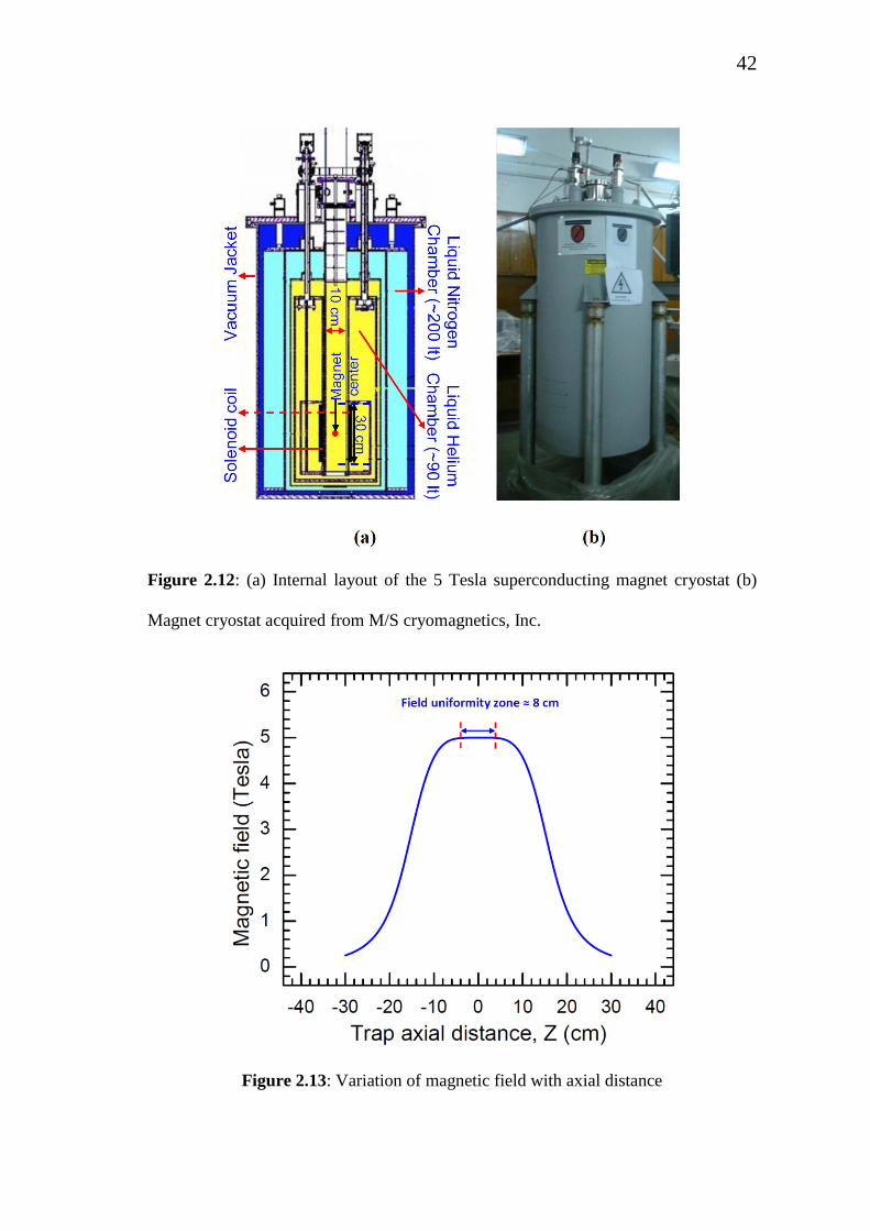
42
Figure 2.12: (a) Internal layout of the 5 Tesla superconducting magnet cryostat (b)
Magnet cryostat acquired from M/S cryomagnetics, Inc.
Figure 2.13: Variation of magnetic field with axial distance

43
5 Tesla superconducting magnet ( persistent mode)
Uniformity 0.1 ppm over 1cm DSV
Temporal stability ~1ppb/hr
Magnetic shielding circuit to provide flux stabilization
2.5.2 Five electrode cylindrical Penning ion trap
A five electrode cylindrical PIT and its typical harmonic potential distribution is
shown in figure 2.14. Here the electrodes abbreviations are defined as, UE: Upper
Endcap, UC: Upper Compensation, R: Ring, LC: Lower Compensation, LE: Lower
Endcap. Different electrodes of the PIT are isolated from each other using a
machineable ceramic dielectric (MACOR). Various geometrical as well as electrical
parameters for trapping of electron in a magnetic field of 5 T are listed in Table 2.1.
As given in Table 2.1, the axial frequency of trapped electrons in this PIT is expected
to be around 63 MHZ with a trap voltage of 10V.
Figure 2.14: (a) A five electrode open ended cylindrical PIT with typical voltage
distribution due to the potentials applied on the electrodes (b) Fabricated assembly.

44
Table 2.1: Estimated parameters of the five electrode cylindrical PIT electrodes
Geometrical Parameters Electrical Parameters
r0 3.29 mm C2 0.65202
Ze 10 mm U0 10 V
Z0 3.04 mm fc 140.16 GHz
Zc 2.12 mm fz 63 MHz
Zg 0.6 mm f+ 140.16 GHz
d 2.71 mm f- 14.15 KHz
2.6 Summary
In this chapter, we have briefly discussed the basics of PIT and its application in
the field of high precision atomic spectroscopy. A simple equivalent circuit model of
the trapped charged particles in a PIT is presented. Furthermore, various detection
techniques and its typical response with trapped charged particles are discussed.
Finally, the description of the cryogenic PIT system at VECC is presented.

45
Chapter-3
Design, implementation and
characterization of a low noise amplifier
3.1 Introduction
Low noise amplifiers (LNAs) are required for amplifying very weak signals.
Essential requirement for an LNA design is to provide signal amplification with
minimum noise contribution. In a PIT, detection of charged particles via the image
current induced on the trap electrodes requires an amplifier with very low noise
characteristics. As the image signal induced due to the oscillating charged particles
can be considered as equivalent to a high impedance source, the amplifier should have
a very high input impedance to boost the weak image signal and develop a large
voltage signal at the amplifier‟s input. This requirement of high input impedance is
feasible using a field effect transistor (FET) as an active device for amplifier
implementation. As the axial oscillation frequency associated with the oscillating
charged particles is expected to be ~ 63 MHz for electron trapping (refer to Table 2.1),
the selected FET should also possess very low input and output capacitances in order
to achieve a bandwidth which is sufficiently high to cover our desired frequency zone
of interest. Both Si and GaAs FET could be used for implementing an LNA satisfying
these technical requirements. However a GaAs based FETs are widely employed due
to its several advantages, for instance, ability to work at extreme cryogenic
temperature of 4K, low power dissipation, very small input and output capacitance
46
and high frequency of operation as compared to those of a Si FET [52–56]. A variety
of GaAs based FET like NE25139 and NE3508 MESFET from NEC, 3SK series
MESFET, ATF35143/ATF34143 pHEMT from Avago technologies are widely used
for amplifier design in a number of ion trap experiments [57–61]. However a GaAs
pHEMT device exhibits much higher transconductance and hence higher voltage gain
along with lower input voltage noise density is achieved as compared to that of GaAs
MESFET or HEMT [55, 61–63]. These properties of GaAs based pHEMT devices
make them a promising candidate for the front stage of an LNA for high frequency
application.
Design and implementation of an LNA with high input impedance based on
Cascode topology [64] (common source stage followed by common gate stage) is
extensively reported in a number of literatures [11, 57–59, 65, 66]. In [57], a dual gate
GaAs MESFET NE25139 is implemented as a cascode amplifier whereas an output
impedance of 50 Ω is achieved by implementing a source follower stage. The work
reported in [58] also implemented a cascode amplifier where the dual gate MESFETs
NE25139 in the first stage and 3SK124 in the second stage forms the cascode pair.
Here both the gates of NE25139 are shorted to increase the channel length which
helps to reduce the flicker noise corner frequency. Additionally the noise contribution
of the amplifier is further reduced by a factor of 0.7 by paralleling two MESFETs in
the first stage, thus helps to achieve an input voltage noise density of
HznV4.0 above 400 KHz. Similar type of amplifier configuration is also used to
detect the charged particles in a beamline [67] where a cascode amplifier with active
load is implemented to increase the amplification factor of the amplifier. One can also
use a simple common source amplifier [60, 61] as it offers several advantages such as

47
lower power dissipation, fewer numbers of power supply modules, lower input
voltage noise density and lower component counts as compared to the cascode
topology. Ref. Rx1 uses a single stage amplifier, implemented using GaAs pHEMT
ATF34143, whose output is directly connected to the room temperature amplifier
using a 50 Ω coaxial cable. In [60], an additional R-L-R network, commonly known
as inductive shunt peaking technique, is implemented in a common source amplifier to
achieve a bandwidth of 60 MHz. In most of the reported work on the amplifier with
high input impedance, amplifier‟s performance is limited by its operating range of
frequency, which is restricted within 100 MHz. A common problem in such
amplifier‟s operation at frequencies above 10 MHz is the voltage gain roll-off due to
the parasitic capacitances of different components mounted on the printed circuit
board (PCB) substrate. Operating these amplifiers in the frequency zone of (60 – 70)
MHz will offer reduced voltage gain as our frequency zone of interest lies in the
falling region of the amplifier‟s frequency response. Several techniques of bandwidth
enhancement are already investigated by the earlier researchers [12, 68–77]. One of
the popular techniques is inductive shunt peaking [12, 70–72]. In this technique, 3-dB
bandwidth of the amplifier is enhanced by neutralizing the effect of equivalent output
capacitance using a load inductance connected in series with the load resistor. The
value of load inductance required to obtain a desired bandwidth can be estimated by
using a simple equivalent circuit model as discussed by Mohan et al [70]. In this
work, the bandwidth enhancement factor (BWEF) (defined as the ratio of 3-dB
bandwidth with finite load inductance to the 3-dB bandwidth with zero load
inductance) of the amplifier is estimated by considering the effect of load inductance,
output capacitance and load resistance. However, this prediction of BWEF is only

48
valid if the drain-source channel resistance is much larger than the load resistance.
The estimation of BWEF becomes incorrect if the value of drain-source channel
resistance is comparable or smaller than the load resistor. Therefore, to obtain an
accurate estimation of BWEF for a given load inductance, which is valid for all values
of drain-source channel resistance and load resistance, an improved equivalent circuit
model, that includes the effect of drain-source channel resistance, is proposed.
In this chapter, the design, development and detailed characterization of an LNA is
presented. The chapter is organized as follows: The major noise contribution in a FET
and its behavior with the variation in operating bias condition is briefly described in
Section 3.2 whereas Section 3.3 gives a brief description of different amplifier
topologies. Initial design of the amplifier based on cascode topology and its test
results are described in Section 3.4. Design, analysis and testing of an inductively
tuned common source amplifier with shunt peaking technique are presented in Section
3.5. Results of the BWEF of the amplifier for different load inductance is presented
and a comparison is drawn between the theoretical model and measured BWEF of the
amplifier. Section 3.6 presents the test result of the inductively tuned common source
amplifier fabricated on an FR4 substrate. The cryogenic testing of the amplifier is
presented in Section 3.7. Finally, the chapter is summarized in Section 3.8.
3.2 Noise sources in a field effect transistor
The electronic noise in a FET operating below 100 MHz is mainly due to two
different noise sources [78, 79]. One of them is the frequency independent thermal
noise generated by the random movement of charge carriers in the drain-source
channel. Another noise source is the flicker noise arising from the fluctuations in
generation and recombination rate of charge carriers in the depletion region of the

49
FET. Flicker noise is also called as 1/f noise, as its spectral noise density is inversely
proportional with the frequency. A typical variation of the spectral noise density for
thermal and flicker noise in a FET is shown in figure 3.1. The dominant electronic
noise in the lower frequency region is contributed by the flicker noise. However it is
not an important issue above the flicker corner frequency, Fc, which is less than 10
Figure 3.1: Thermal and flicker noise behavior in a FET
MHz for most of the commercially available FETs. Therefore in our frequency range
of (60 – 70) MHz, the effect of channel thermal noise will dominate. The input
thermal voltage noise density in a FET is expressed as,
m
ng
kTv
4 (3.1)
where, T is the operating temperature, γ is the FET thermal noise coefficient and gm is
the transconductance of the FET which can be expressed in terms of drain current Id as
dss
dmom
I
Igg (3.2)
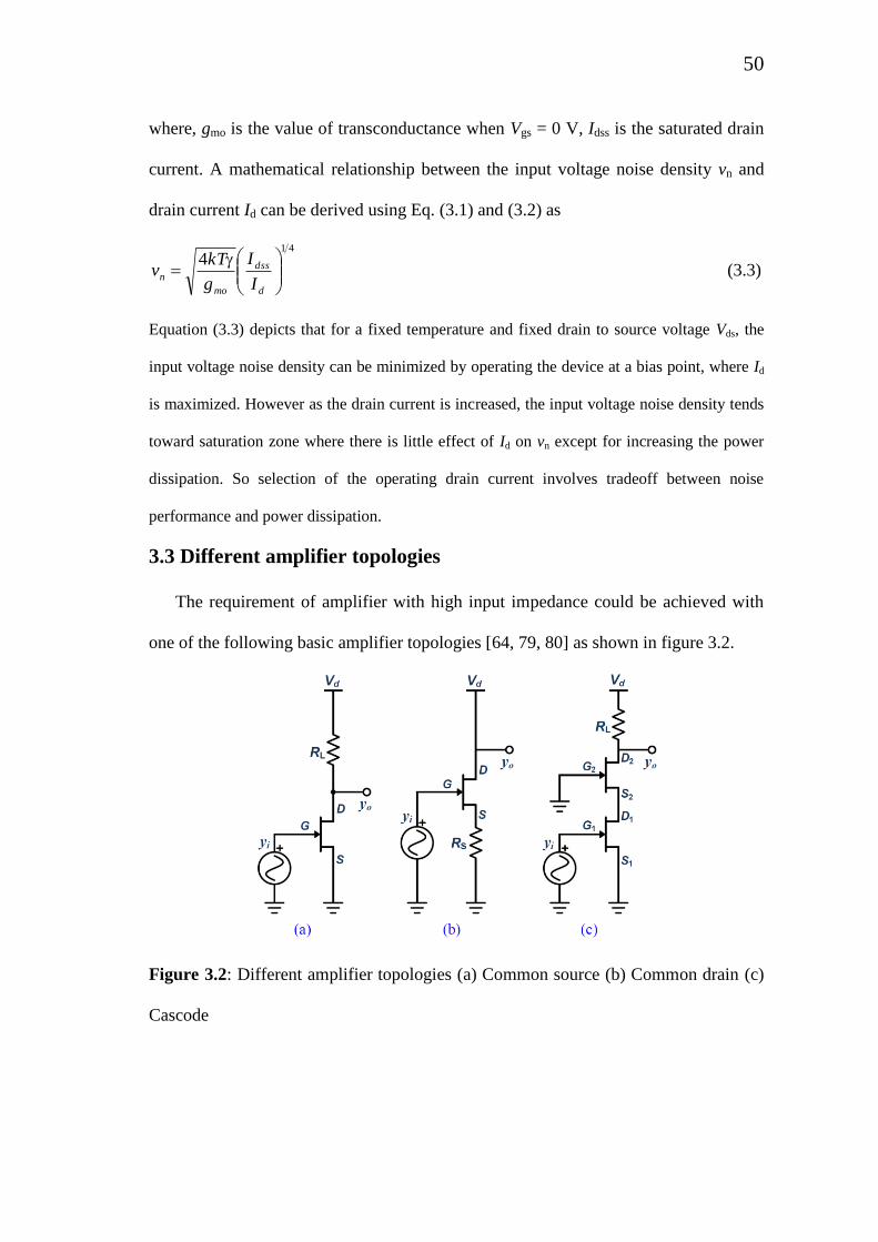
50
where, gmo is the value of transconductance when Vgs = 0 V, Idss is the saturated drain
current. A mathematical relationship between the input voltage noise density vn and
drain current Id can be derived using Eq. (3.1) and (3.2) as
41
4
d
dss
mo
nI
I
g
kTv (3.3)
Equation (3.3) depicts that for a fixed temperature and fixed drain to source voltage Vds, the
input voltage noise density can be minimized by operating the device at a bias point, where Id
is maximized. However as the drain current is increased, the input voltage noise density tends
toward saturation zone where there is little effect of Id on vn except for increasing the power
dissipation. So selection of the operating drain current involves tradeoff between noise
performance and power dissipation.
3.3 Different amplifier topologies
The requirement of amplifier with high input impedance could be achieved with
one of the following basic amplifier topologies [64, 79, 80] as shown in figure 3.2.
Figure 3.2: Different amplifier topologies (a) Common source (b) Common drain (c)
Cascode

51
A common source topology (Figure 3.2(a)) is one of the most simple and
commonly used configurations for high impedance amplifier design. Its reasonable
voltage gain (~ 5 – 10) along with very high input impedance (~ MΩ) makes it a
potential candidate for the amplification of weak image signal at the first stage. Some
of the major limitations of this topology are increased input and output capacitance
due to the miller effect and poor reverse isolation which might result into oscillation.
Another topology which offers very high input impedance is common drain
topology as shown in figure 3.2(b). However the amplifier implemented in this
topology offers a voltage gain which is less than unity; this configuration is mostly
used for impedance matching at the final stage as it offers very low output impedance.
A cascode is a two stage amplifier topology implemented using the cascade
connection of a common source topology and common gate topology. Some of the
major advantages of this topology are its higher voltage gain due to increased output
impedance and better reverse isolation as compared to a common source topology.
However it results in increased power dissipation as compared to a common source
amplifier.
3.4 Design of a low noise cascode amplifier
LNA based on cascode topology has been extensively used for weak image signal
detection in a PIT. In line with the standard circuit design for a cascode LNA reported
in [57, 59], initially a low noise cascode amplifier is designed and implemented. The
detailed circuit schematic of the amplifier and its test results are given in the following
sections.

52
3.4.1 Circuit schematic and fabrication
A number of GaAs FET, like NE3508M05 [81], NE25139 [82], ATF34143 [83]
and ATF 35143 [84], are extensively used in various ion trap experiments [57-60,
Rx1]. The technical specifications of these FETs are explored through their datasheet
and it is observed that NE3508M04 has very low noise characteristics (Noise Figure ~
0.45 dB typical) along with a very low value of gate to source leakage current (~ 1 μA
typical). However due to the difficulty in procurement of this particular FET, a GaAs
pHEMT ATF34143 from Avago Technologies with similar noise characteristics
(Noise Figure ~ 0.5 dB typical) is chosen for our amplifier design. The circuit
schematic of the cascode amplifier is shown in figure 3.3. The first stage of the
cascode amplifier is based on a very low noise pHEMT, Q1, implemented using ATF-
34143. The second stage of the cascode amplifier is implemented using a low noise
MESFET 3SK240, Q2, manufactured by Toshiba [85]. In order to match the
Figure 3.3: Circuit schematic of the low noise Cascode amplifier.

53
impedance of cascode amplifier at node ‘a’ (refer to Figure 3.3) with the impedance of
transmission line and higher stage electronics (usually 50Ω impedance), a source
follower amplifier is implemented using ATF-34143 in the third stage. The source
follower stage along with 32Ω resistor at the terminal Vout offer an output impedance
of 50Ω. During the amplifier‟s operation, the drain-source voltage Vab and Vbc of FET
Q1 and Q2 is always maintained at 1V for a given operating drain current Id. All the dc
biasing lines are filtered using low pass RC circuits to filter out the noise in the dc
supply lines. Surface mount device (SMD) components are used for the amplifier
implementation to minimize the component‟s parasitic reactance. Finally, the
amplifier is fabricated on a low loss Teflon PCB [86] as shown in figure 3.4.
Figure 3.4: The fabricated LNA on a Teflon substrate 1 Input , 2 First stage FET,
3 Second stage FET, 4 Third stage FET, 5 Output.
3.4.2 Voltage gain measurement
The frequency response of the LNA is measured in the span of (0.1-200) MHz for
various operating drain currents (Id) ranging from 0.5 mA to 3 mA. To avoid operation
of amplifier in the saturation region, the input signal is first attenuated by ~ 60 dB and

54
Figure 3.5: The scheme of experimental setup for frequency response measurement
Figure 3.6: Voltage gain with frequency for different value of drain currents
then fed to the amplifier. The block schematic for measurement of frequency response
is shown in figure 3.5. The voltage gain variation with frequency of the amplifier for
different values of drain current ranging from 0.5 mA to 3 mA is shown in figure 3.6.
It is observed that voltage gain of the amplifier increases with the increase in
operating drain current. The maximum voltage gain of the amplifier is found to be ~
13.8 at a drain current of 3 mA in the frequency range of (1-10) MHz. A 3-dB
bandwidth of (0.2 – 62) MHz is obtained at 3 mA.

55
3.4.3 Noise measurement
We have measured the input voltage noise density of the amplifier as a function of
drain current Id. The equivalent input voltage noise density of the amplifier is
measured by two different techniques. In the first technique, a spectrum analyzer is
used to measure the equivalent input voltage noise density. Noise measurement using
this technique requires a high-end spectrum analyzer with very low noise spectral
density. Due to very limited number of such high-end facilities with us, it is difficult
to use such facilities frequently, whenever it is required to measure the noise
performance of the amplifier. Therefore, we have developed an alternate low cost
noise measurement test setup comprising of a mixer and data acquisition card (DAQ)
interfaced with LabVIEW software. The noise measurement using this technique is
also benchmarked with the measurement using spectrum analyzer. The noise
measurement techniques using spectrum analyzer and DAQ card is described in the
following sections.
3.4.3.a Noise measurement using spectrum analyzer:
The equivalent input voltage noise density of the amplifier is measured using a
spectrum analyzer from Rhode & Schwarz. Here the equivalent input voltage noise
density of LNA is measured by terminating the input of the amplifier with a source
resistor 50SR and measuring the output noise power of the amplifier. In order to
increase the output noise power of LNA above the DANL (Displayed Average Noise
Level) of the spectrum analyzer HzdBm142 , the noise power is further amplified
using an LNA (ZFL-500LN) as shown in figure 3.7. By measuring the final output
noise power, Pn,o, the noise figure (NF) of the amplifier is then calculated as [87]:

56
Figure 3.7: Noise measurement scheme
KTBdBGHzdBmPdBNF onF 1000log10log10 10,10 (3.4)
where 21GGG is the combined voltage gain, Pn,o is the amplified output noise
power per unit bandwidth and F is the noise factor. Subsequently, the input voltage
noise density en,eq is obtained as [87],
14, FKTBRe Seqn (3.5)
Here F is the noise factor. Since the amplifier used in the noise amplification stage of
the test setup has a low noise characteristics HznVen 8.02 , the measured
equivalent input voltage noise density en,eq will be close to the input voltage noise
density en,1 of the LNA under test.
3.4.3.b Noise measurement using DAQ card:
A low cost noise measurement test-setup has been developed to measure the input
voltage noise density of the amplifier. A block diagram of the test-setup is illustrated
in figure 3.8. In this test setup the equivalent input voltage noise density of LNA is
measured by terminating the input of the amplifier with a source resistor 50sR
and measuring the amplified output noise voltage. In order to increase the output noise
voltage of LNA above the DANL of the DAQ card, the noise voltage is further
amplified using two LNAs: ZFL-500LN from Mini-Circuits HznVen 8.02 and

57
Figure 3.8: Block diagram of the test setup for noise measurement.
Dual-A3-7b from Stahl-electronics HznVen 23 . The amplified output noise
voltage en,o for unit bandwidth is expressed as:
2
3
2
3,
2
2
2
2,
2
1
2
1,
2
, 4 GeGeGeKTRe nnnSon (3.6)
which is further simplified to,
2
2
2
1
2
3,
2
1
2
2,2
1,
22
, 4GG
e
G
eKTReGe
nn
Snon
(3.7)
where 321 GGGG is the combined voltage gain. The amplified output noise voltage
(en,o) is downconverted to an intermediate frequency of 5 kHz using a mixer ZX05-
1HW from Mini-Circuits. The downconverted noise signal is then acquired using a
DAQ card NI-PCI-4472 [88] interfaced with LabVIEW 8.5 software, which
automatically sweeps the local oscillator (LO) frequency and acquires the noise data
in the frequency range of (10-80) MHz. Subsequently, the voltage noise density en,in is
obtained by dividing the amplified output noise voltage by the resultant voltage gain
of the amplifier chain. Finally the equivalent input voltage noise density en,eq of the

58
amplifier is obtained by subtracting the thermal noise of the source resistor from the
voltage noise density en,in and it is given as:
S
on
Sinneqn KTRG
eKTRee 44
2
,2
,,
(3.8)
Since the amplifier used in the 2nd
and 3rd
stage of the test setup has a low noise
characteristics, the measured equivalent input voltage noise density en,eq will be close
to the input voltage noise density en,1 of the LNA under test.
Using the above two techniques, the equivalent input voltage noise density of the
amplifier is measured at different drain currents in the span of 0.5 mA to 3 mA and the
measured results are shown in figure 3.9. The measured noise characteristic of the
amplifier using both the techniques is in good agreement within HznV2.0 . The
measured equivalent input voltage noise density of the amplifier shows a frequency
independent behavior in the frequency band of 30 MHz to 80 MHz. It is important to
note that the equivalent input voltage noise density shows a decreasing behavior for a
drain current in the range of 0.5 mA to 1.5 mA. Whereas, there is little effect of drain
current on the equivalent input voltage noise density beyond mAI d 5.1 . The
equivalent input voltage noise density at mAI d 5.1 is measured to be HznV8.1 .
3.5 Design of a low noise inductively tuned common source amplifier
One of the key challenges in the design of an amplifier with broadband frequency
response that reaches up to few hundreds of megahertz is to achieve a higher 3-dB
cutoff frequency, which is mainly restricted by the parasitic capacitance of different
components mounted on the PCB substrate. Several techniques are reported which

59
Figure 3.9: Equivalent input voltage noise with different drain current. (a) Measured
with DAQ card (b) Measured with spectrum analyzer.
enhances the bandwidth of an amplifier by compensating the effect of output
capacitance using an inductance. Some of the typically used bandwidth enhancement
techniques are series peaking, shunt peaking and shunt-series peaking. The basic
circuit topologies to implement these techniques are illustrated in figure 3.10. Here, C1
is the output capacitance of the FET, C2 is the load capacitance which may include the
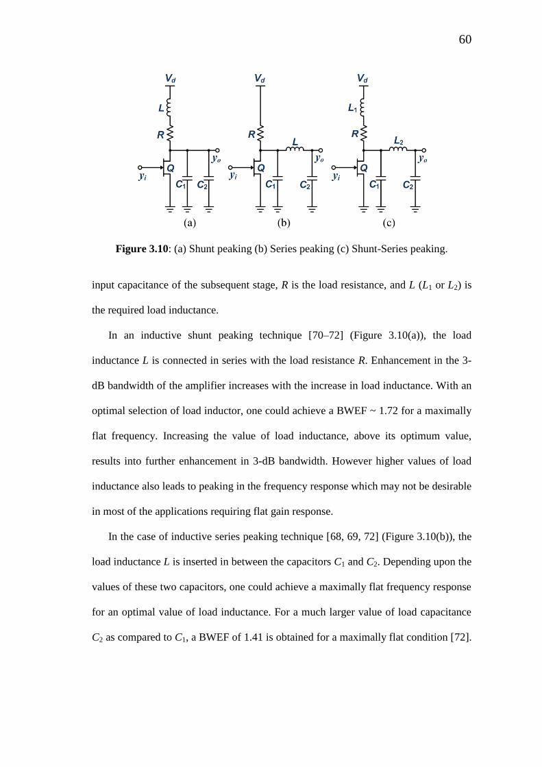
60
Figure 3.10: (a) Shunt peaking (b) Series peaking (c) Shunt-Series peaking.
input capacitance of the subsequent stage, R is the load resistance, and L (L1 or L2) is
the required load inductance.
In an inductive shunt peaking technique [70–72] (Figure 3.10(a)), the load
inductance L is connected in series with the load resistance R. Enhancement in the 3-
dB bandwidth of the amplifier increases with the increase in load inductance. With an
optimal selection of load inductor, one could achieve a BWEF ~ 1.72 for a maximally
flat frequency. Increasing the value of load inductance, above its optimum value,
results into further enhancement in 3-dB bandwidth. However higher values of load
inductance also leads to peaking in the frequency response which may not be desirable
in most of the applications requiring flat gain response.
In the case of inductive series peaking technique [68, 69, 72] (Figure 3.10(b)), the
load inductance L is inserted in between the capacitors C1 and C2. Depending upon the
values of these two capacitors, one could achieve a maximally flat frequency response
for an optimal value of load inductance. For a much larger value of load capacitance
C2 as compared to C1, a BWEF of 1.41 is obtained for a maximally flat condition [72].

61
However one could obtain a BWEF of 2 for a maximally flat frequency response
with 12 3CC [69].
Combining both the shunt peaking and series peaking results in inductive shunt-
series peaking technique [72, 73] (Figure 3.10(c)) that offers significant enhancement
in bandwidth as compared to simple shunt peaking or series peaking technique. Using
shunt-series peaking, one could achieve much larger BWEF of 3.51 for a maximally
flat frequency response with 12 5.1 CC [72].
The prediction of BWEF in the above mentioned techniques is based on the
frequency domain analysis of a simple equivalent circuit model that includes the effect
of load inductances L1 and L2, output capacitances C1 and C2, and load resistance R.
However, one of the major drawbacks in these models is that it does not include the
effect of drain-source channel resistance of FET. The predicted BWEF using those
models is only valid for the case where drain-source channel resistance is much larger
than the load resistance. Therefore an accurate estimation of BWEF, which is valid for
all values of drain-source channel resistance and load resistance, requires an improved
circuit model that includes the effect of drain-source channel resistance.
The next section presents an improved model to predict the BWEF of an amplifier
with inductive shunt peaking technique. The shunt peaking technique is chosen
because its BWEF remains unaffected by the capacitive load conditions (i.e., ratio of
C1 to C2) as compared to a series/shunt-series peaking technique [77]. Also, a shunt
peaking technique uses only a single inductor as compared to shunt-series peaking
technique and offers a BWEF which is sufficient for our application. The shunt
peaking technique is implemented in a low noise common source amplifier as it offers
lower power dissipation, fewer numbers of power supply modules, lower input

62
voltage noise density and lower component counts. Additionally, the circuit modeling
for accurate prediction of BWEF and its correlation with the test results is easy to
analyze in a common source amplifier due to its simple design as compared to a
cascode topology.
3.5.1 Improved model of a common source amplifier with inductive shunt
peaking
We consider a simple common source amplifier with load inductance as shown in
figure 3.11. Here gm is the transconductance of the FET, R is the load resistance, Req is
the parallel combination of drain-source resistance (rd) and R, Cp is the parasitic
capacitance associated with the inductor L, Co is the equivalent output capacitance that
includes the effect of output capacitance of FET C1 and load capacitance C2
21 CCCo and oeq
ococ
CRf
2
1
2
is the upper 3-dB cut-off frequency at
zero load inductance. The small signal ac current im yg can be expressed as
Figure 3.11: A common source amplifier with load inductance and its equivalent
circuit.

63
RLCssLR
LCs
rsCsysyg
p
p
d
ooim 2
211 (3.9)
The voltage gain of the amplifier can be obtained using Eq. (3.9) and it is given by
)()()()(
)()()(
23
2
ddodppdodop
dmdmmdp
L
i
o
rRsrRCLsrCRCrCLsRrCLC
RrgsLrgsgRrLCsH
sy
sy
(3.10)
Assuming that the reactance of Cp pCp CX 1 is significantly large as compared to
the reactance of L LX L , we obtain
)()()(
)()(2
ddodo
dmdm
LrRsrRCLsrLC
RrgsLrgsH
(3.11)
Defining the parameter m as,
eq
oc
oeqoeq
eq
R
L
CR
L
CR
RLm
2
(3.12)
The value of inductance L can be written as
oc
eq
oeq
mRCmRL
2
(3.13)
Rearranging Eq. (3.11), we obtain
2
2 1
11
2
11
1
1)()(
srR
ms
RrrR
m
srR
RgmRg
sH
docddoc
doc
eqm
eqm
L
(3.14)
Assuming voltage gain eqmV RgA as well as oc to be unity for the case of
0m (zero load inductance), the transfer function obtained from Eq. (3.14) gets
simplified to,

64
2
2 111
1
11
srR
ms
rR
Rmr
srR
m
sH
dd
d
d
L
(3.15)
Rearranging Eq. (3.15), we obtain
asbas
as
m
ns
n
n
m
ns
m
ns
sH L
)(1
1
1
1
22
(3.16)
where, drRn , mna )1( and )1( nnb . It can be easily verified from Eq.
(3.16) that the maximum achievable BWEF for a nearly flat frequency response is ~
1.72 provided that Rrd ( 0n ). This value of BWEF is obtained for 41.0m .
However, if the value of rd is comparable or smaller than R, the maximum value of
BWEF becomes a function of parameters m and n. Eq. (3.16) is used to plot the
frequency response of an inductive shunt peaked amplifier for two different cases of rd
while keeping the load resistance R fixed at 1kΩ. Figure 3.12(a) shows the frequency
response for the case of significantly large rd as compared to R Rrd 20 . The
condition 0m indicates zero load inductance without any bandwidth enhancement
whereas the condition 45.0m gives a maximally flat frequency response with
BWEF ~ 1.7. Increasing the value of m above 0.45 results into gain peaking which
may be undesirable in most of the applications. Figure 3.12(b) shows the frequency
response for the case of Rrd . It can be seen here that the BWEF for a maximally flat
frequency response reduces to ~ 1.44 for the case of Rrd . It is easy to observe from
figure 3.12 that the value of m required to achieve maximally flat frequency response
depends on the load condition (rd and R) and it is different for the two cases of rd. The

65
Figure 3.12: Frequency response of a common source amplifier with inductive shunt
peaking (a) krkR d 20,1 (b) krkR d 1,1 .
Figure 3.13: Variation of maximum BWEF as a function of rd.
variation of BWEF for a maximally flat frequency response as a function of rd is
plotted in figure 3.13. The plot in figure 3.13 clearly indicates that the maximum
achievable BWEF for flat gain condition drops as the value of rd decreases with
respect to the load resistor R. The values of BWEF for any combination of the

66
parameters m and n can be directly calculated by solving Eq. (3.16). Transforming the
Laplace domain into the complex frequency domain, Eq. (3.16) reduces to,
baja
jajH L
2 (3.17)
The magnitude of the transfer function given in Eq. (3.17) can be written as,
2222
22
baa
ajH L
(3.18)
Therefore the upper 3-dB cut-off frequency of the amplifier with load inductance L
Lc can be found by solving the following equation,
2
1
2
102222
22
jH
baa
aL
LcLc
Lc (3.19)
As the upper 3-dB cut-off frequency with zero load inductance L 0c is taken as
unity, Lc will be equal to BWEF of the amplifier. Solving for Lc using Eq. (3.19)
we get,
2
41212 2222
aababaaBWEF Lc
(3.20)
Eq. (3.20) gives a simple closed form expression for direct calculation of BWEF of
the amplifier.
3.5.2 Circuit schematic and fabrication
We have designed and tested an inductively tuned common source amplifier. The
amplifier is implemented using ATF-34143 device from AVAGO technologies. The
circuit schematic of the amplifier is shown in figure 3.14. The amplifier consists of
two stages. The first stage is implemented in common source topology to provide
signal amplification while the second stage is implemented in common drain topology

67
Figure 3.14: Circuit schematic of the inductively tuned common source amplifier.
to offer an output impedance of 50 Ω. During the operation of amplifier, drain-source
voltage (Vde) of FET Q1 is always maintained at 1V, and this condition is realized by
selecting a supply voltage Vdd1 as obtained by applying Kirchhoff's voltage law (KVL)
to the loop “abcde”. Next, the desired drain current Id1 is set by varying the gate
voltage Vg1. For the second stage FET Q2, the supply voltage Vdd2 is fixed at 3V and
the gate voltage Vg2 is kept at ground potential. This fixes the drain current Id2 at 5 mA
with the drain-source voltage at 2V. The inductor L helps to extend the 3-dB
bandwidth of the amplifier by neutralizing the effect of equivalent output capacitance
at node “d.” The values of L used in the circuit are in the range of (0-1.2) μH with
parasitic capacitance, Cp, ~ 0.16 pF. Because of very low value of Cp, reactance of Cp
(XCp) is considerably large enough as compared to reactance of L (XL) above 100
MHz and it will not significantly affect the prediction of BWEF, which is based on the
assumption that LCp XX . For a maximum load inductance of 1.2 μH, ratio of XCp
to XL is still large (~ 3.5) at a frequency of 200 MHz. With the chosen inductor in our
design, it has been found that the predicted BWEF using Eq. (3.20) is accurate within

68
less than 1.7 % as compared to the BWEF predicted including the effect of Cp. All the
dc biasing lines uses low pass RC circuits to filter out the noise in the dc supply lines.
These RC circuits will only contribute low frequency poles and zeros that would not
affect the high frequency performance of the amplifier. All the components used in the
implementation of the amplifier are chosen to be of surface mount type because of
their low parasitic inductances and capacitances. Finally, the amplifier is fabricated on
a low dielectric loss Teflon substrate [86] as shown in figure 3.15.
3.5.3 Voltage gain measurement
Scheme for voltage gain measurement of an amplifier is already described in
Section 3.4.2. The frequency response of the amplifier is measured in the range of
(0.1-240) MHz at discrete values of drain current Id1 , that are spaced 1mA apart, in a
span of 1mA to 5 mA. Moreover, at each of these drain current settings, the frequency
response is also measured as a function of load inductance. The frequency response of
the amplifier with different load inductance is shown in figure 3.16. The plots show
that the 3-dB bandwidth of the amplifier increases with the increase in load inductance
from 0 μH to 1.5 μH. However the frequency response in figure 3.16(f) for a load
inductance of 1.5 μH shows a slight gain peaking ~ 0.2 dB. Therefore, the inductance
Figure 3.15: The fabricated amplifier on a Teflon substrate, 1 Input, 2 First stage
FET, 3 load inductance, 4 Second stage FET, 5 Output.

69
Figure 3.16: Measured frequency response with different load inductance
Figure 3.17: A typical frequency response of the amplifier at mAId 11

70
value has been kept within 1.2 μH in the circuit. Bandwidth enhancement of the
amplifier can be clearly understood from the plot shown in figure 3.17. It can be seen
from the graph that 3-dB bandwidth of the amplifier shows an increasing trend with
the increase in the load inductance. This bandwidth enhancement can be linked to the
increase of upper 3-dB cut-off frequency with the variation in load inductance from 0
µH to 1.2 µH. There is no significant change observed in the lower 3-dB cut-off
frequency with the addition of load inductance. The parameters rd , fc-o and maximum
voltage gain (Am) are measured at different drain currents with zero load inductance.
These results are summarized in Table 3.1. It can be noted here that rd decreases by a
factor of ~ 5 and Am increases by a factor of ~1.4 as the drain current is changed from
1 mA to 5 mA. It is easy to understand here, that the decrease in rd with the variation
in drain current causes fc-o to increase from 92 MHz to 158 MHz, which amounts to an
increase in the bandwidth by a factor of ~1.7. The 3-dB bandwidth of the amplifier is
calculated from the measured frequency response and it is summarized in Table 3.2.
The BWEF is calculated from the measured bandwidth as a function of load
inductance and drain current. The predicted BWEF as obtained from Eq. (3.20) is
Table 3.1: The measured parameters of the amplifier
Id1 (mA) rd (Ω) fc-o (MHz) Am
1 1000 92 4.28
2 500 116 5.05
3 333 136 5.62
4 250 142 5.81
5 200 158 5.96

71
Table 3.2: Measured 3-dB bandwidth with different load inductance and drain current
Measured 3-dB bandwidth (MHz)
L (μH)
Id1 (mA)
0.00
0.56
0.78
1.00
1.20
1 (0.2 – 92) (0.2 – 110) (0.2 – 116) (0.2 – 132) (0.2 – 134)
2 (0.2 – 116) (0.2 – 138) (0.2 – 142) (0.2 – 158) (0.2 – 160)
3 (0.2 – 136) (0.2 – 146) (0.2 – 160) (0.2 – 166) (0.2 – 168)
4 (0.2 – 142) (0.2 – 163) (0.2 – 168) (0.2 – 186) (0.2 – 186)
5 (0.2 – 158) (0.2 – 172) (0.2 – 186) (0.2 – 194) (0.2 – 192)
compared with the experimentally obtained values of BWEF as shown in figure 3.18.
It can be observed from the plot that a maximum BWEF of ~1.46 is obtained with a
load inductance of 1.2 µH, at a drain current of 1 mA. As drain current is increased
further, the BWEF reduces and reaches to ~1.25 at a drain current of 5mA. This
happens due to the variation in rd with the drain current, which consequently changes
the BWEF. Additionally, the maximum BWEF of ~1.46 reduces with decrease in load
inductance and reaches to ~1.2 at a load inductance of 0.56 µH. Moreover, for all
drain current settings, as the load inductance is increased above 0.56 µH, initially
BWEF increases and then gets saturated at a load inductance of 1 µH and only (1-2) %
variation is observed in the BWEF for a change in load inductance from 1.0 µH to 1.2
µH.
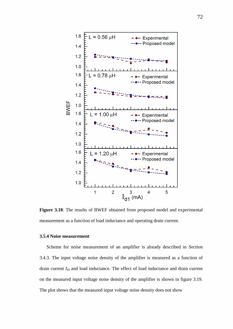
72
Figure 3.18: The results of BWEF obtained from proposed model and experimental
measurement as a function of load inductance and operating drain current.
3.5.4 Noise measurement
Scheme for noise measurement of an amplifier is already described in Section
3.4.3. The input voltage noise density of the amplifier is measured as a function of
drain current Id1 and load inductance. The effect of load inductance and drain current
on the measured input voltage noise density of the amplifier is shown in figure 3.19.
The plot shows that the measured input voltage noise density does not show

73
Figure 3.19: Variation of input voltage noise density with Id1 (a) HL 0 (b)
HL 1
significant change with the addition of a 1 μH load inductor. Moreover, the input
voltage noise density also shows a frequency independent behavior above 10 MHz. It
is also observed that the input voltage noise density is high HznV4.2~ at a lower
drain current of 1 mA. However the amplifier shows an improved noise performance
as the drain current is increased above 2 mA. Also there is no significant effect of
drain current on the noise performance of the amplifier above 2 mA. An input voltage
noise density HznV2.02 is obtained for a drain current in the range of (2 – 5)
mA. The typical performance parameters of the amplifier for a load inductance of 1
μH are illustrated in Table 3.3.

74
Table 3.3: Typical performance parameters of inductively tuned CS LNA
Id1 (mA) Am fc-L (MHz) HznVe eqn, Power dissipation (mW)
1 4.28 132 2.4 17.1
2 5.05 158 2.1 21.4
3 5.62 166 2.1 27.9
4 5.81 186 2.0 36.6
5 5.96 194 2.0 47.5
3.6 Inductively tuned common source LNA fabrication and testing
The circuit schematic, fabricated Teflon PCB and test result of the inductively
tuned common source amplifier has already been described in Section 3.5. One of the
critical issues in the fabricated PCB, shown in figure 3.15, is its open copper trace.
This might lead to several problems like oxide and corrosion formation, unintended
electrical shorts which may affect the performance of the amplifier. Therefore, the
amplifier has been fabricated with solder mask on an FR4 substrate and it is shown in
figure 3.20. The measured frequency response of the amplifier for Id1 = 1mA with two
different values of load inductance is shown in figure 3.21. It is observed that the
maximum voltage gain in the flat frequency region (1 MHz – 10 MHz) of the
amplifier remains unaffected by the substrate of the PCB. However the 3-dB
bandwidth of the amplifier reduces for an FR4 substrate due to its higher dielectric
constant, which leads to large parasitic capacitances, as compared to a Teflon
substrate. For instance, the higher 3-dB cut-off frequency, fc, at Id1 = 1 mA reduces
from 92 MHz for Teflon substrate to 60 MHz for FR4 substrate. With a load
inductance of 1.5 μH, the higher 3-dB cut-off frequency further enhances to 85 MHz

75
Figure 3.20: The fabricated amplifier on an FR4 substrate
Figure 3.21: Frequency response of the amplifier with variation in L at Id1 = 1 mA
(BWEF ~ 1.42). The input voltage noise density of the amplifier is also measured for
the fabricated PCB and it is found that the noise performance of LNA are not
dependent on the material of the PCB substrate.
3.7 Cryogenic testing of LNA
The cryogenic testing of the LNA at a temperature of 130K has been performed in
a cryogenic test setup. The test setup consists of a vacuum chamber placed within a
cryogenic Dewar filled with liquid nitrogen (LN2) as shown in figure 3.22. Three

76
Figure 3.22: Cryogenic test setup for characterization of LNA (a) 3D sectional view
(b) Fabricated assembly (c) LN2 Dewar
Figure 3.23: LNA circuit mounted with SS disc

77
numbers of resistance temperature detector (RTD) sensors are mounted with a glass
rod to monitor the level of LN2 within the cryogenic Dewar. The LNA board is
mounted on to a SS circular disc within the vacuum chamber as shown in figure 3.23.
One RTD sensor has also been used to monitor the temperature of the LNA circuit
board. The required DC signals for biasing the LNA are routed through 9-pin vacuum
feedthrough. The input and output RF signals are routed through lemo feedthrough.
These feedthroughs are mounted on ISO-KF 40 flange as shown in figure 3.24. For
testing of LNA at cryogenic temperature, initially the vacuum chamber was evacuated
using a rotary pump. Once a vacuum of ~ 0.01 mbar is attained, the cryogenic Dewar
is filled with the LN2. The level of LN2 is maintained upto a required height till the
temperature of the LNA board gets saturated after few hours. Conductive as well as
radiative cooling mechanism helps to cool down the LNA board to 130K in 5-6 hours.
The LNA is tested without any load inductance. The frequency response of the
LNA is measured over a frequency range of 100 KHz – 100 MHz. The measured
frequency response of the LNA at Id1 = 1 mA is shown in figure 3.25. It clearly
demonstrates that the voltage gain of the LNA increases by a factor of 1.5 once the
amplifier is cooled down to 130K. A maximum voltage gain of 4.3 is obtained at room
temperature whereas voltage gain ~ 6.5 is achieved at 130K. A higher 3-dB cut-off
frequency of 64 MHz is obtained at 130K which is slightly larger as compared to 60
MHz obtained at room temperature.
Figure 3.24: Vacuum feedthroughs for signal routing

78
Figure 3.25: Frequency response of LNA at Id1 = 1 mA
Figure 3.26: Input voltage noise density of LNA at Id1 = 1 mA
The measured noise characteristic of the LNA at Id1 = 1 mA is shown in figure
3.26. Figure 3.26 clearly shows that the noise performance of the LNA improves and
the input voltage noise density decreases by a factor of 1.7 after cooling down the
amplifier to 130K. Although the input voltage noise density is large in the frequency

79
band of 1 MHz to 8 MHz due to the presence of flicker noise, it reduces and is
frequency independent beyond 10 MHz. An input voltage noise density ~
HznV6.2 is obtained at room temperature whereas it improves to ~ HznV5.1 at
130K.
Table 3.4 lists the key technical specifications of the LNA with high input
impedance that are used not only in Penning ion trap but also in various other
applications like NMR spectroscopy, charged particle detection and as a microchannel
plate detector. In Table 3.4, the typical performance parameters of the designed LNA,
with an operating drain current of 1 mA in the first stage, is also illustrated. With
inductive shunt peaking implemented on a Teflon substrate, a bandwidth of 132 MHz
is achieved which is sufficient for electron detection in VECC PIT. The input voltage
noise density for most of the reported LNA operating below 77K is less than
HznV1 . In this chapter, cryogenic testing of LNA at a temperature of 130K is
presented. The input voltage noise density reduces to HznV5.1 at 130K and it is
expected to reduce below a level of HznV1 at 4K. As seen in Table 3.4, the power
dissipation of the designed LNA is ~ 17 mW which is much larger as compared to
those reported in other works where power dissipation does not exceed the level of 10
mW. With the current biasing condition of the LNA with inductive peaking, the power
dissipation in the first stage is only 2.1 mW, whereas the second stage, operated using
a 3V drain supply with a bias current of 5 mA, contributes 15 mW in the total power
dissipation. It is observed that the voltage gain and output impedance of the designed
LNA does not change significantly if the second stage is operated using a 1.5V drain
supply with a bias current of 4 mA. Therefore the second stage could also be operated
using 1.5V supply to reduce the total power dissipation to ~ 8 mW.

80
Table 3.4: Comparison of typical performance parameters of the designed LNA with
recent works on LNA with high input impedance. RT: Room Temperature
Application Amplifier
Topology
Gain
(V/V)
Noise
(nV/√Hz)
Bandwidth
(MHz)
Power
Dissipation
(mW)
Operating
Temperature
(K)
NMR
Spectroscopy
[4]
NA 5 3.4 95 30 RT
Single proton
detection in a
PIT [57]
Cascode 8.9 0.83 NA 4.5 4
mass-ratio
measurements
in a PIT [59]
Cascode 6.16 0.5 NA 3 4
FTICR mass
spectrometry
in a PIT [60]
Inductiv-
ely tuned
Common
Source
5.6 1 60 6 77
Charged
particles
detection in a
beamline [67]
Cascode 3.2 0.8 5.5 NA 4
Timing
microchannel
plate detector
[89]
10 0.8 150 NA RT
Present work Cascode 7.6 2.3 58 18.2 RT
Present work Inductiv-
ely tuned
Common
Source
(PTFE
substrate)
4.3 2.4 132 17.1 RT
Present work Inductiv-
ely tuned
Common
Source
(FR4
substrate)
4.3 2.6 85 17.1 RT
Present work Common
Source
(FR4
substrate)
4.3
@RT
6.5@
130K
2.6@RT
1.5@
130K
60@RT
64@130K
17.1 RT-130K

81
3.8 Summary
In this chapter, we have presented the design, implementation and detailed
characterization of an LNA. Initially the LNA is implemented in cascode topology
and its voltage gain and input voltage noise density are measured. To increase the 3-
dB bandwidth of the amplifier, an inductive shunt peaking technique is employed in a
common source amplifier that offers much larger bandwidth as compared to that
obtained in a cascode amplifier. We have also presented an improved as well as a
generalized equivalent circuit model, which includes effect of drain source resistance
rd for the accurate prediction of BWEF in a common source amplifier with shunt
peaking technique. We showed experimentally that BWEF increases with the increase
in load inductance and decreases with the increase in drain current. Moreover, the
maximum BWEF is reached at lower values of drain currents (∼1 mA) with a load
inductance in the vicinity of 1 μH, but at the cost of a lower voltage gain. The BWEF
obtained from the measured frequency response for different combinations of load
inductance and operating drain current agrees well within 5% of the estimated values
from the improved model. The input voltage noise density of the amplifier is also
measured using a low cost test setup and a spectrum analyzer. An input voltage noise
density of ~ HznV1.2 is achieved at Id = 2 mA in our frequency region of interest.
The amplifier is also successfully tested at 130K which shows an improved
performance in terms of voltage gain as well as input voltage noise density of the
LNA. The LNA presented in this paper are general in nature and will be very useful in
the design and analysis of wide band high frequency common source amplifier for
different applications.

82
Chapter-4
Design and development of Colpitts
oscillator for Penning ion trap
4.1 Introduction
The electrical characteristic of the PIT geometry is essential for the design of
detection circuit and estimation of the number of trapped particles. It is known that the
trapped ions are in a dynamic equilibrium in a PIT, performing an oscillatory motion,
which is a superposition of three harmonic motions in ideal condition. So, the strength
of image signal induced on the trap electrodes depends on the trap geometry and
number of ions present in the trapped condition. PIT geometry can be electrically
represented as a lumped capacitor in parallel with a very high resistance (~ few GΩ)
contributed mainly by the dielectrics separating different electrodes of PIT. However
one can neglect the effect of dielectric resistive loss and assume the PIT assembly as a
pure capacitance at high frequencies. Therefore, the value of this capacitive
impedance is important for the signal estimation as well as in the design of the
resonant based detection circuit.
Several techniques to measure the capacitance of a device have been investigated
and reported in literature. The most commonly used ones are charge-discharge method
[90 – 92], auto-balancing bridge method [93, 94], RF I-V method [94], network
analysis method [94], and LC resonance method [95–97]. Capacitance measurement
using charge-discharge method is a simple and low cost solution where capacitance is

83
measured by recording the RC time constant of the circuit. However this technique
has several drawbacks such as low sensitivity, low signal to noise ratio (SNR) and
large measurement offset [91]. The basic capacitance measurement scheme in most of
the commercially available LCR meter and impedance analyzer employs auto-
balancing bridge method [94]. These instruments usually employ an operational
amplifier (OP-AMP) to configure a simple I-V converter circuit whose output voltage
is proportional to the capacitor under test (CUT). However measurement of
capacitance above 1 MHz employs a complex circuitry consisting of a null detector, a
phase detector and a vector modulator to ensure high measurement accuracy upto a
few hundreds of MHz. These instruments provide much higher sensitivity and SNR as
compared to a charge-discharge method. Capacitance measurement in a very high
frequency region (~ GHz) could be achieved using an RF I-V method or network
analysis method. Capacitance measurement using RF I-V method is based on the
direct measurement of voltage across the CUT and current flowing through the CUT.
In order to ensure optimum performance at very high frequency region, it employs an
impedance-matched measurement circuit and a high precision coaxial test port. This
technique is usually employed in the commercially available RF impedance analyzer
which covers a frequency range of 1 MHz to 3 GHz. One can go beyond 3 GHz using
network analysis method where capacitance measurement is based on the
measurement of incident and reflected wave. Measurement sensitivity using this
technique is much superior as compared to RF I-V method for a narrow impedance
range where the impedance of CUT is close to the characteristic impedance of the
measurement circuit. However an RF I-V method offers much better accuracy and
sensitivity for a wide range of impedance as compared to a network analysis method.

84
Another widely used technique to measure the capacitance of a device is using a high
Q RLC resonant circuit [95–97]. In this technique, the CUT is incorporated as a circuit
element of either a series or parallel resonant circuit driven by an external signal
source. The value of CUT is measured by observing the shift in amplitude, phase or
resonant frequency of the circuit. One could measure the capacitance very precisely
by observing the shift in resonant frequency as compared to an amplitude shift or
phase shift techniques. However, one of the drawbacks of this technique is that it
requires a very high Q resonant circuit to achieve a very good sensitivity and
resolution. Another alternative of resonant based technique for capacitance
measurement is using an LC oscillator where CUT is placed as a part of the frequency
deciding network (oscillator's LC circuit) and the value of CUT is measured by direct
observation of shift in oscillation frequency. One of the potential advantage of this
technique is that it does not require an external signal source. Additionally,
capacitance measurement using an LC oscillator is more accurate compared to a
simple resonant based technique as the measurement is not affected by the Q of the
frequency deciding network. However, this technique requires an LC oscillator with
very good frequency stability [97].
A standard impedance analyzer can be used to measure the capacitance of the PIT
assembly before it is placed within the evacuated chamber. However, for an accurate
measurement of trap capacitance in the evacuated chamber using an impedance
analyzer, a standard fixture with long compensated cables and bandwidth higher than
the axial frequency of oscillation are required. Moreover, small mechanical
movements of the long compensated cables result in erroneous capacitance
measurement. Also the electrical feedthrough in between the impedance analyzer and
85
the PIT assembly inhibits the use of proper compensated cable. Therefore, an in-situ
measurement of trap capacitance, if feasible, qualifies as a good alternative for such
an application.
In this chapter, a Colpitts oscillator [98, 99] is designed for in-situ measurement of
trap capacitance. One of the other types of LC oscillators is Hartley oscillator which
uses inductive voltage divider in the feedback path. The stability of the oscillator is
affected due to variation in self and mutual inductance in the feedback path. In
comparison, Colpitts oscillator uses capacitive voltage divider in the feedback path
producing much better stability and purer sinusoidal signal at very high frequencies
[98, 99].
This chapter documents the design and implementation of a Colpitts oscillator
based in-situ capacitance measurement scheme for the PIT assembly. In addition, the
same in-situ Colpitts oscillator can be used to provide RF excitation during the
detection process. This, in turn, eliminates the need of providing RF power from an
external RF signal generator through the electrical feedthrough on the PIT enclosure.
The organization of the chapter is as follows: Section 4.2 describes the detailed design
of the Colpitts oscillator, the buffer amplifier and the low pass filter; Section 4.3
presents the capacitance measurement scheme using Colpitts oscillator; Section 4.4
reports the performance analysis and test results of the Colpitts oscillator module;
Section 4.5 reports the trap capacitance measurement results; Section 4.6 presents the
trap capacitance measurement and the trapped particle detection schemes; and Section
4.7 gives a brief summary of this chapter.

86
4.2 Design and implementation of Colpitts oscillator module
A Colpitts oscillator module with an oscillation frequency in the vicinity of 63
MHz is developed as shown in figure 4.1. The complete circuit module is
implemented in three stages. The first two stages form a Colpitts oscillator circuit
followed by a buffer stage with 50Ω impedance output. The output of the buffer stage
is then filtered using a low pass filter (LPF) at the third stage to reduce the total
harmonic distortion (THD) at the oscillator output. A detailed description of the
circuit is given in the following sub-section.
Figure 4.1: Schematic of the Colpitts oscillator with Buffer amplifier and LPF.
4.2.1 Colpitts oscillator
The first stage of the measurement circuit is a Colpitts oscillator implemented
using an npn bipolar junction transistor (BJT) BF199 (Q1) [100]. Here Q1 is
configured in common base topology. The key advantage of this topology is its non-
inverting characteristics which minimizes the additional parasitic capacitance due to
miller effect. Therefore a common base configuration is a good option for high
frequency oscillator design. The series capacitors )100,10( 21 pFCpFC in
parallel with the inductor L )150( nHL forms the tank circuit which will decide the

87
resonant frequency of the oscillator. In order to provide a feedback signal required for
oscillation, a small portion of the oscillatory signal at the collector terminal „p‟ is fed
back to the emitter terminal „q‟ (refer to figure 4.1) via the capacitive voltage divider
C1 and C2. Here Cu is the unknown capacitance to be measured. A trimmer capacitor
CT is connected between the emitter terminal „q‟ and ground to tune the oscillation
frequency of the Colpitts oscillator during trapping and detection process. The
resonant frequency of the oscillator is expressed as,
u
T
T
o
CCCC
CCCL
f
21
212
1
(4.1)
As the value of capacitance C1 is much smaller than that of C2, the output oscillatory
signal of the Colpitts oscillator is taken from the emitter terminal „q‟. This will reduce
the effect of higher stage electronics on the resonant frequency of the Colpitts
oscillator.
4.2.2 Buffer amplifier
The second stage of the measurement circuit is a unity gain buffer amplifier
implemented using a closed loop buffer IC BUF602 from Texas Instruments [101]. Its
high input impedance (~ 1 MΩ) along with very low output impedance (~ 1.4 Ω)
serve the purpose of impedance matching between the output impedance of the
Colpitts oscillator at terminal „q‟ with the input impedance of the transmission line
and higher stage electronics (usually 50 Ω). It also improves the frequency stability of
the circuit by reducing the loading effect from the higher stages. The first and second
stages of the measurement circuit (Colpitts oscillator and buffer amplifier) are
fabricated on an FR4 substrate as shown in figure 4.2. An SMA port is provided for
connecting the unknown capacitor Cu.

88
4.2.3 Low pass filter
In order to suppress the higher order harmonics, the output of the buffer amplifier
is filtered through an LPF at the third stage. A Butterworth LPF is implemented to
achieve a maximally flat response. The design specification for this filter is
determined by its cut-off frequency (fc) and minimum stopband attenuation at a
predefined frequency fs. As the measurement circuit will be operated near the axial
frequency of trapped electrons (~ 63 MHz), fc is selected as 75 MHz. Also, a
Figure 4.2: Colpitts oscillator and buffer amplifier fabricated on an FR4 substrate.
minimum stopband attenuation of 30dB at MHzf s 126 (second harmonic
corresponding to the electron axial signal) is sufficient to suppress the higher order
harmonics in our case. The design parameters of the filter is calculated as [102]
68.1c
ss
f
f (4.2)
33.6log2
110log
10
1.0
10
s
LAS
n
(4.3)
500
00
g
Z for 10 g
(4.4)

89
gLc
c0
(4.5)
0
gC
c
c
(4.6)
Here, is a frequency variable of Butterworth low pass prototype filter, c is
normalized cut-off frequency, n is the order of the filter, 0 is the impedance scaling
factor, Z0 is the source impedance, g is the prototype element values. It can be
Figure 4.3: Schematic of a 7th order Butterworth LPF.
Table 4.1: Design parameters for the Butterworth LPF
Prototype element values Design Parameters Components used
g1 0.445 C1 18.88 pF 18 pF
g2 1.247 L1 132.3 nH 130 nH
g3 1.8019 C2 76.475 pF 68 pF
g4 2 L2 212.2 nH 200 nH
g5 1.8019 C3 76.475 pF 68 pF
g6 1.247 L3 132.3 nH 130 nH
g7 0.445 C4 18.88 pF 18 pF

90
observed from Eq. (4.3) that a 7th order filter, as shown in figure 4.3, is required to
achieve our design specification. The actual design parameters for the 7th order
Butterworth LPF are summarized in Table 4.1. Depending on the availability of the
capacitors and inductors, the LPF is implemented using the components as listed in
the Table 4.1. Using the aforesaid values, the transfer function of the LPF can be
written as
765432
1
HsGsFsEsDsCsBsAsH
(4.7)
Table 4.2 lists the coefficient values of the filter transfer function given by Eq. (4.7).
The LPF is characterized by a dominant pole pair at 8100581.50252.1 i and the
relative stability analysis yields a gain margin of 6.03 dB and phase margin of infinity.
The LPF is implemented on an FR4 substrate as shown in figure 4.4. An FFT of the
oscillator signal, as observed at the output of the buffer amplifier, is shown in figure
4.5 (a). The frequency of oscillation is ≈ 66.7 MHz. The THD is around 2.3%. The
second harmonic has the highest power content, roughly 33dB lower than that at
fundamental frequency. The performance of the measurement circuit coupled with
LPF, as given in figure 4.5 (b), shows marked improvement in the output signal. The
higher order harmonics are almost suppressed and the THD improves to 0.22%.
Table 4.2: Coefficient values of filter transfer function
A 2 E 3410503.4
B 81078.1 F 4310233.6
C 171091.7 G 5210625.5
D 2510267.2 H 6110531.2

91
Figure 4.4: Fabricated LPF on an FR4 substrate.
Figure 4.5: Frequency spectrum of the signal (a) at Buffer Output (b) after LPF.
4.3 Capacitance measurement scheme
The oscillation frequency of a Colpitts oscillator is decided by the resonant
frequency of the parallel LC circuit implemented using L, C1 and C2. However, at
higher frequencies, the parasitic capacitances and inductances associated with the
circuit also affects the oscillation frequency. Therefore it is required to measure the
effective capacitance, Ceff and the effective inductance, Leff of the circuit. These two
circuit parameters can be extracted by measuring the oscillation frequency of the

92
Colpitts oscillator with and without a known value of capacitive load. The oscillation
frequencies fo and fs, with and without a known capacitor Cs are expressed as
effeff
oCL
f2
1
(4.8)
)(2
1
seffeff
sCCL
f
(4.9)
Using Eq. (4.8) and Eq. (4.9) the effective capacitance, Ceff and effective inductance,
Leff are calculated as
1
2
s
o
seff
f
f
CC
(4.10)
effo
effCf
L2
2
1
(4.11)
If a capacitance Cu is placed in the unknown capacitor slot, the oscillation frequency fu
becomes
)(2
1
ueffeff
uCCL
f
(4.12)
Using Eq. (4.11) and Eq. (4.12) the unknown capacitance, Cu is calculated as
1
2
u
oeffu
f
fCC
(4.13)
Thus any unknown capacitor Cu can be measured using Eq. (4.13) once the circuit
parameter Ceff is determined. To measure the capacitance of the PIT facility, the trap is
connected as the unknown capacitance Cu and its value is determined using Eq. (4.13).

93
4.4 Colpitts oscillator performance and test results
As the Colpitts oscillator circuit serves the dual purpose of measuring the trap
capacitance and supplying RF power to the trapped electrons during excitation and
subsequent detection, a number of static and dynamic performance indices are
evaluated to quantify its performance. Static performance indices include amplitude
and frequency stability; accuracy and standard deviation of measurement; sensitivity,
resolution and repeatability of the oscillator. Whereas, the dynamic performance
indices evaluated are the warm-up time and response time. To facilitate the
measurement procedure for evaluation of the aforesaid performance indices, a
standard capacitor bank, as shown in figure 4.6, is fabricated. This capacitor banks
consists of SMD capacitors in the range of 0.5–3.3 pF. The cable shown in figure 4.6
is used to connect these SMD capacitors with the unknown capacitor port of the
Colpitts oscillator module. Repeated measurement data for each capacitor are acquired
using the Colpitts oscillator circuit and are used to compute the performance indices.
Figure 4.6: SMD capacitors mounted on an FR4 PCB

94
4.4.1 Amplitude and frequency stability
Amplitude and frequency stability are the two key performance indices for a
Colpitts oscillator. Large fluctuations in oscillation frequency will cause error in the
measurement of unknown capacitance. Stable performance of the oscillator in terms of
amplitude and frequency is also required when it is used to excite the trapped charged
particles. In general, stability is measured in terms of the fluctuations in the oscillation
frequency over a fixed interval of time in its steady state operation. These fluctuations
are mainly caused due to the shift in the values of different circuit parameters and
supply voltages which are used to power up the circuit. A typical variation of the
oscillation frequency and amplitude over a large number of samples taken in a fixed
Figure 4.7: (a) Typical fluctuation in frequency and (b) its statistical distribution

95
Figure 4.8: (a) Typical fluctuation in amplitude and (b) its statistical distribution.
interval of time after the circuit reaches steady state, and the corresponding histograms
of these data are shown in figure 4.7(a), figure 4.7 (b) and figure 4.8 (a), figure 4.8 (b).
It is observed from the histograms that the fluctuation in the frequency measurement
(3σ value) in the steady state operation is ~ 90 Hz around the centre frequency of
66.57946 MHz and that in amplitude measurement (3σ value) is less than 0.6% of the

96
mean value of ~ 233.07 mV. Both the figures indicate acceptable amplitude and
frequency stability of the oscillator.
4.4.2 Accuracy and standard deviation
Accuracy of measurement is the closeness of the measured value to the true value
of the measured variable. In the capacitance measurement procedure, the true value of
the CUT is taken to be the one measured with a standard measuring instrument, viz. a
50 MHz impedance analyzer from Keysight Technologies. Since we have an apriori
knowledge of the error sources that would contribute to the final measurement error,
we present the following procedure to estimate the measurement error.
In order to estimate the uncertainty in the capacitance measurement, it is required
to calculate the error propagation due to various parameters which are involved in the
measurement. It is easily observed from Eq. (4.13) that accuracy in the measurement
of any unknown capacitor will depend on the stability and measurement accuracy of fu
and fo along with the accuracy in the extracted parameters Ceff. Therefore, we need to
first calculate the error propagation in the value of Ceff. Measurement error in the
value of Ceff, as given in Eq. (4.10), can be obtained as
2
2
222
2
1
2
s
o
s
s
o
o
s
o
s
seffeff
ff
fdf
fdf
ff
C
dCCdC
(4.14)
Once the measurement uncertainty in the value of Ceff is known, uncertainty in the
measured value of unknown capacitor Cu, as given in Eq. (4.13), can be obtained as

97
2
2
222
2
1
2
u
o
u
u
o
o
u
o
eff
eff
uu
ff
fdf
fdf
ff
C
dCCdC
(4.15)
However, as given in Eq. (4.14), measurement uncertainty in the value of Ceff depends
also on the accuracy with which the value of the capacitor Cs is known to us.
Therefore we first calculated the uncertainty in the value of Cs (Cs is chosen as 2.2 pF)
by taking 200 consecutive measurements using a high precision impedance analyzer
along with a high frequency test fixture, both from M/S Keysight Technologies. The
statistical distribution in the measured value of Cs is plotted in figure 4.9.The plot
shows that uncertainty in the measured value of capacitor Cs is ±0.0013pF (3σ value).
As described in Section 4.4.1, uncertainty in the oscillation frequencies (fo, fs and fu) of
the Colpitts oscillator has been measured by taking a large number of samples in a
fixed interval of time after the circuit reaches steady state. The measurement
Figure 4.9: Statistical distribution of measured capacitance using impedance analyzer.

98
uncertainty in the value of Ceff, as calculated using Eq. (4.14), turns out to be ±0.0186
pF. The values of f0, fs, Cs, Ceff and their uncertainties are listed in Table 4.3. Finally,
using Eq. (4.15) and the values listed in Table 4.3, the error in the measured value of
unknown capacitor, Cu, is estimated. Typical measurement data for Cu in the range of
0.5–3.3 pF is given in Table 4.4.
Table 4.3: Measurement uncertainty in the value of Ceff
fo (MHz) 68.51240 Cs (pF) 2.2585
Δfo (MHz) 0.00007 ΔCs (pF) 0.0013
fs (MHz) 66.22764 Ceff (pF) 32.1782
Δfs (MHz) 0.00010 ΔCeff (pF) 0.0186
Table 4.4: Measurement uncertainty in the value of Cu
Cu (pF)
(Impedance analyzer) 0.4837 1.0218 1.8669 3.3383
fu (MHz) 67.97653 67.40659 66.57946 65.12010
Δfu (MHz) 0.00009 0.00006 0.00009 0.00011
u
u
f
f 61032.1
61089.0 61035.1
61069.1
Cu (pF)
(Colpitts oscillator) 0.5093 1.0644 1.8955 3.4398
ΔCu (pF) 0.0003 0.0006 0.0011 0.0020
u
u
C
C 41089.5
41064.5 41080.5
41081.5

99
4.4.3 Sensitivity and resolution
The sensitivity of any measuring instrument can be defined as the ratio of the
statistical fluctuation in the measured parameters to its mean value. As the capacitance
measurement using Colpitts oscillator is based on the measurement of its oscillation
frequency, therefore sensitivity, in this particular case, is defined as ff which
corresponds to sensitivity of CC in terms of capacitance measurement. Sensitivity
of the Colpitts oscillator is already listed in Table 4.4 which clearly shows that the
measurement circuit has almost an uniform sensitivity over the entire range of
capacitance measurement.
Resolution of any measuring instrument is defined as the ability of the
measurement circuit to differentiate between the smallest changes in the measured
parameter. Resolution of the capacitance measurement circuit in our case can be
defined as f which corresponds to resolution of C in terms of capacitance
measurement. A typical capacitance measurement of 1 pF shows a resolution of
0.0006 pF (refer to Table 4.4).
4.4.4 Repeatability
Repeatability of a measurement process is its ability to achieve closeness amongst
multiple measurement data. In determining the repeatability error in the measurement
process, sixteen set of measurements for each value of the standard SMD capacitors in
the range of 0.5–3.3 pF were carried out using the Colpitts oscillator and a 50 MHz
impedance analyzer from Keysight Technologies. The true value of these capacitors is
taken to be the one measured by the impedance analyzer. The mean values as well as
the repeatability error of the multiple measurements of SMD capacitor using the
Colpitts oscillator and impedance analyzer are illustrated in Table 4.5 which shows
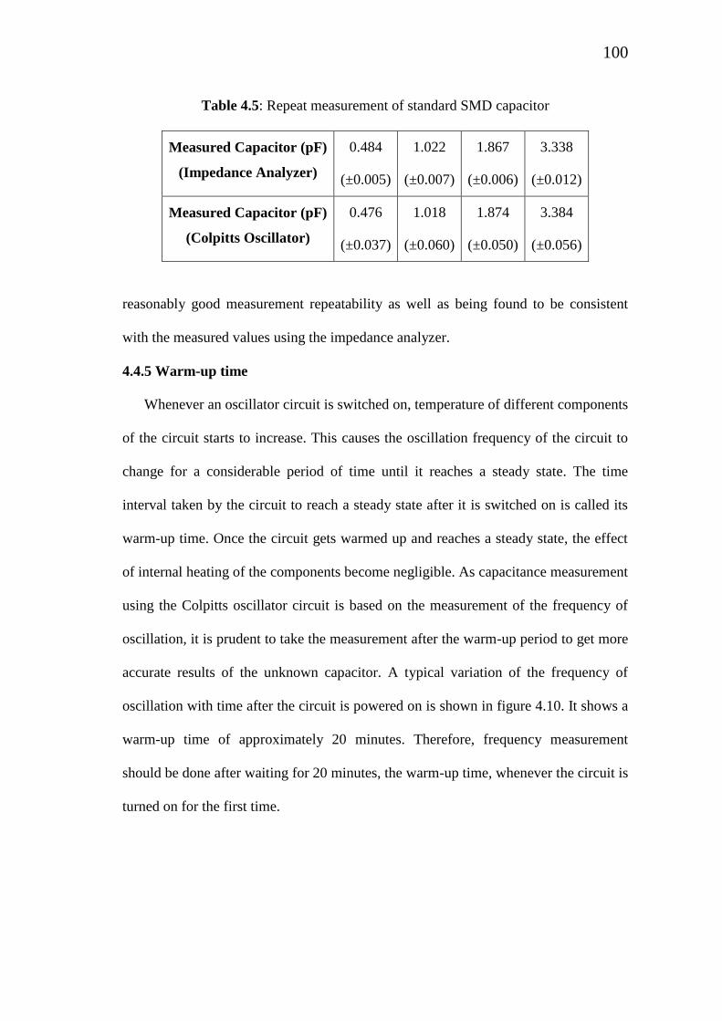
100
Table 4.5: Repeat measurement of standard SMD capacitor
Measured Capacitor (pF)
(Impedance Analyzer)
0.484
(±0.005)
1.022
(±0.007)
1.867
(±0.006)
3.338
(±0.012)
Measured Capacitor (pF)
(Colpitts Oscillator)
0.476
(±0.037)
1.018
(±0.060)
1.874
(±0.050)
3.384
(±0.056)
reasonably good measurement repeatability as well as being found to be consistent
with the measured values using the impedance analyzer.
4.4.5 Warm-up time
Whenever an oscillator circuit is switched on, temperature of different components
of the circuit starts to increase. This causes the oscillation frequency of the circuit to
change for a considerable period of time until it reaches a steady state. The time
interval taken by the circuit to reach a steady state after it is switched on is called its
warm-up time. Once the circuit gets warmed up and reaches a steady state, the effect
of internal heating of the components become negligible. As capacitance measurement
using the Colpitts oscillator circuit is based on the measurement of the frequency of
oscillation, it is prudent to take the measurement after the warm-up period to get more
accurate results of the unknown capacitor. A typical variation of the frequency of
oscillation with time after the circuit is powered on is shown in figure 4.10. It shows a
warm-up time of approximately 20 minutes. Therefore, frequency measurement
should be done after waiting for 20 minutes, the warm-up time, whenever the circuit is
turned on for the first time.

101
Figure 4.10: Warm-up time of the Colpitts oscillator.
4.4.6 Response time
The response time of an instrument is defined as the time taken by the measuring
instrument to reach within a specified band of its steady state value after the
measurement parameter is changed from one value to another. For the case of
capacitance measurement using Colpitts oscillator, the circuit requires much less time
as compared to the warm-up period to settle to a new value if the capacitance is
switched from one value to another. Figure 4.11 (a) illustrates the response of the
Colpitts oscillator for different capacitance values whereas figure 4.11 (b) shows a
typical response of the circuit when a 0.5pF capacitor is placed in the unknown
capacitor slot after the circuit is warmed-up. The oscillation frequency of the Colpitts
oscillator settles down to a frequency of (68.1912 ± 0.0003) MHz within a response
time of less than 4 minutes.

102
Figure 4.11: (a) Response of the Colpitts oscillator for different capacitors. (b)
Typical response when capacitance is switched just after the warm-up period.
4.5. Measurement of trap capacitance
A special arrangement has been made for measuring the capacitance of PIT
assembly and inter electrode capacitance as shown in figure 4.12.Two PCBs are
mounted very close to the PIT assembly in order to reduce the length of the copper
wire connecting trap electrode with mounted PCB. While PCB-A is mounted to
measure the capacitance between upper endcap (UE) to lower endcap (LE), PCB-B
are used to measure capacitance between other trap electrodes, viz. „upper
compensation (UC)‟ and „ring (R)‟. A sample capacitor Cs (2.2 pF) is mounted to
determine the value of Ceff and Leff. In line with the measurement procedure
documented in Section 4.3, a known capacitance Cs, with a measured value of 2.2585
pF, is first connected to extract the Ceff and Leff of the oscillator tank circuit. Here Ceff
and Leff are the total effective capacitance and inductance seen at the collector

103
Figure 4.12: PIT assembly with PCB mounted to facilitate its capacitance
measurement.
terminal of BJT Q1 (refer to figure 4.1) which includes the effect of tank circuit
associated with the Colpitts oscillator along with the coaxial cable and pins mounted
on the PCB for connecting the capacitors. The value of Ceff and Leff measured with this
setup are 29.39 pF and 169.39 nH respectively. Once the value of Ceff and Leff is
determined, trap electrode is connected with the unknown capacitor port and its
capacitance value is determined.
Capacitance measurement of trap assembly using the impedance analyzer is
difficult to achieve due to its complicated geometry, and measurement errors occur if
trap electrodes are connected with the standard fixture with uncompensated leads.
Therefore, we have used an alternate resonance based technique to verify the accuracy
of our measurement of the trap capacitance. In this technique, a high Q helical
resonator (Details of the helical resonator are given in Chapter-5) is used. In order to
measure the unknown capacitance, the capacitor is placed outside the helical resonator

104
Figure 4.13: (a) Capacitance measurement scheme. (b) Fabricated resonator.
assembly and it is connected with the open end and outer shield of the helical
resonator using a small coaxial cable. The resultant tank circuit is then driven at its
resonance point using an external RF source as shown in figure 4.13 (a). A similar
approach as applied in the case of the Colpitts Oscillator has been used to compute the
value of capacitance using the read-out of the resonant frequency and the values of
Ceff and Leff. The measured values of standard capacitors and trap capacitance using
helical resonator and Colpitts oscillator are given in Table 4.6. Measured results using
both the techniques are found to be in good agreement with each other.
Table 4.6: Mean value and the repeatability error in the measured value of Trap
capacitance using helical resonator and Colpitts oscillator
Capacitors
(pF)
Measured (pF)
(Helical Resonator)
Measured (pF)
(Colpitts Oscillator)
0.5 0.494(±0.045) 0.476(±0.037)
1.0 1.018(±0.037) 1.018(±0.060)
3.3 3.280 (±0.046) 3.384(±0.056)
Trap (UE-LE) 2.228 (±0.038) 2.150 (±0.039)
Trap (UC-R) 3.991 (±0.084) 4.005 (±0.064)

105
4.6 Trap capacitance measurement and trapped particle
detection scheme
In order to execute the two-fold applications using Colpitts oscillator without
disturbing the circuit arrangement, an in-situ capacitance measurement set-up along
with the arrangement for exciting the trapped particles during detection process is
proposed as illustrated in figure 4.14.
During trap capacitance measurement, the upper and lower endcaps (UE and LE)
of the PIT are connected as a load at the collector terminal of the Colpitts oscillator
and the high Q tank circuit is disconnected from the end-cap pair. This is done by the
RF-switches (SW-226 from MACOM) „SW1‟ and „SW2‟, where position 'b' of the
switch ensures the same. The output of the Colpitts oscillator module is routed
through the switch “SW3” and taken out through the electrical feedthrough for
measurement. In the detection process, the UE-LE pair is connected with the tank
circuit through the switch „SW2‟ while the switch „SW3‟ couples the output of LPF
Figure 4.14: In-situ trap capacitance measurement and particle detection scheme.
106
with the tank circuit. The output of the tank circuit is passed through an LNA for
necessary amplification and taken out via the electrical feedthrough for detection of
electronic trapping. The detection process is ensured by putting the RF-switch in
position 'a'. The RF-switches are controlled by a 2–bit external logic input signal
coming via the electrical feedthrough.
4.7 Summary
This chapter presents the design and development of a high frequency Colpitts
oscillator for in-situ capacitance measurement of a PIT facility. The key design
features like oscillator stability, warm-up time, accuracy and standard deviation,
sensitivity, resolution and repeatability of the oscillator are analyzed with the help of
experimental observations. The experimental data shows that the measured sensitivity
of ~ 41089.5 is uniform over our desired capacitance measurement range of 0.5–
3.3 pF. For the case of capacitance measurement of PIT assembly, the measured
capacitance with Colpitts oscillator is verified using an alternate resonance based
technique implemented with a high Q helical resonator. The measured results using
both the techniques are in good agreement. Based on the experimental observations,
the designed Colpitts oscillator, with a very low THD of ~ 0.22% along with its high
sensitivity and resolution, is well suited for low value capacitance measurement of
PIT and also qualifies for providing a clean RF energy at the desired frequency of
interest during the ion detection process. Finally, the scheme for implementation of in-
situ capacitance measurement as well as detection of trapped particles is discussed.

107
Chapter-5
Design and study of a loaded helical
resonator
5.1 Introduction
A high Q resonator is a key component in an ion trapping system. In a Penning
trap, the resonator boosts the weak image signal induced on the trap electrodes. There
are primarily three configurations of a high Q resonant circuit, which are widely used
by RF designers. The lumped resonator, which is implemented using lumped elements
and can achieve a Q of less than 200. The quarter wave coaxial resonator [103], that
consists of two hollow conductors shorted at one end. It can achieve a Q in the range
3000-5000. The helical resonator [103, 104], which consists of two coaxial
conductors, with inner conductor in the form of a helix. It is more compact as
compared to coaxial resonator and can achieve a Q of ~1200. The helical resonator is
the preferred choice in many ion trap experiments, due to its compact size and
reasonably high Q. As the capacitive contribution from the ion trap and amplifier will
affect the resonator performance, it is required to study the effect of capacitive loading
on the behavior of helical resonator. Although Siverns et al. [105] predicted the
resonant frequency of a helical resonator with capacitive loading, which is further
modified by Deng et al. [106], there is no such literature which presents the model
validation with finite element simulations. This chapter presents a simulation
approach to study a capacitively loaded helical resonator using high frequency

108
structure simulator (HFSS). A comparative study is done between the estimated,
simulated and experimental resonant frequency.
In this chapter, we have presented the design, simulation and experimental studies
of a capacitively loaded helical resonator. The chapter is organized as follows: Section
5.2 presents a brief description of a quarter wave resonator. The basic principle and
theoretical design parameter of a quarter wave helical resonator is described in Section
5.3. The HFSS simulation of the capacitively loaded helical resonator and its
comparison with the experimental measurements are discussed in Section 5.4. Finally,
the chapter is summarized in Section 5.5.
5.2 Quarter wave resonator
Quarter wave resonator is a section of two conductor transmission line where the
conductors are short-circuited at one end in order to achieve a parallel type of
resonance [107]. The length of the transmission line is exactly λ/4 for a desired
resonant frequency. Consider a λ/4 section of lossy transmission line, which is shorted
at one end, as shown in figure 5.1 (a). Assuming the transmission line with small loss,
the input impedance near the resonance can be written as [107],
CjRjl
ZZ in
21
1
2 0
0 (5.1)
Here is the attenuation constant of the line, is the phase constant of the line, Z0 is
the characteristic impedance and 00 2 f is the resonant frequency of resonator.
Equation (5.1) clearly represents the form similar to the impedance of a parallel RLC
resonant circuit. The equivalent circuit parameters (R, L, C) and Q of a quarter wave
resonator can be expressed in terms of transmission line parameters and it is given as,

109
Figure 5.1: (a) Quarter wave resonator realization using short-circuited transmission
line (b) Voltage and current distribution along the line (c) Equivalent circuit model of
quarter wave resonator (d) Typical frequency response of resonator
l
ZR
0 (5.2)
008
1
ZfC (5.3)
0
2
02
f
ZL
(5.4)
lRCQ
40 (5.5)
A simple way to realize a quarter wave resonator is by using a coaxial
transmission line with its inner conductor shorted with the outer conductor at one end
of the line [103]. The resonant frequency of a coaxial resonator is completely
determined by the physical length of the coaxial line which is exactly equal to 4 at

110
Figure 5.2: A quarter wave coaxial resonator
its resonant frequency. A basic quarter wave coaxial resonator is shown in figure 5.2.
For a given resonant frequency and outer conductor diameter, one could obtain a
maximum unloaded Q with an optimum ratio of 59.3ab and it is given as [103],
fbQ 398.80 (5.6)
A quarter wave coaxial resonator finds its application in most of the RF system
operating above 1 GHz, as it offers much high Q as compared to a lumped resonator.
However one of the major disadvantages of a coaxial resonator is its large physical
dimension for an operating frequency below 1 GHz.
A quarter wave type of resonance could also be achieved using a helical resonator
where the straight inner conductor of a quarter wave coaxial resonator is replaced with
a helical structure [104]. Although a helical resonator gives lower Q as compared to a
coaxial resonator, one could still achieve a reasonably high Q in a compact geometry
using a helical resonator. A detailed description of a helical resonator is given in
Section 5.3.
5.3 Quarter wave helical resonator
A quarter wave helical resonator is a coaxial transmission line with helical inner
conductor where one end of the helix is shorted with the outer conductor [104]. Due to

111
Figure 5.3: A quarter wave helical resonator
the helical structure of the inner conductor, the phase velocity of the wave travelling
along the helix is much lower as compared to the velocity of light. This in turn
reduces the guided wavelength which makes it possible to have a resonator with a
very good Q below 1 GHz in a compact geometry. A simple quarter wave helical
resonator is shown in figure 5.3. Here, D is the outer shield diameter, L is the outer
shield height, d is the helix diameter, b is the helix height, d0 is the wire diameter and t
is the pitch of the helix winding. The basic transmission line parameters of a helical
line are summarized below [105, 108, 109].
5.0
0
5.2201
1
dtdc
vV
p
f (5.7)
14ln60
0 dbV
Zf
(5.8)

112
fZd
dbl
00
2.08125.7
(5.9)
fg V
122
0
(5.10)
bDdtdLh
221025.0 (5.11)
ddbd
bCc
27.008.01126.054.2 (5.12)
b
dDCs
log
75.0 (5.13)
where c is the velocity of light in cm/sec, vp is the wave velocity along the helix in
cm/sec, 0 is the free space wavelength in cm, g is the guided wavelength in cm, Vf
is the velocity factor, Z0 is the characteristic impedance in Ω, is the attenuation
constant, is the phase constant, f is the frequency in MHz, Lh is the helix inductance
in μH, Cc is the self capacitance of helix in pF and Cs is the helix to shield capacitance
in pF. Here all dimensions of the helical resonator, shown in figure 5.3, are in inches.
5.3.1 Design parameter
A helical resonator at a given resonant frequency could be designed in various
ways by controlling the parameters of the inner helical structure. However, there is an
optimum ratio of helix diameter to outer shield diameter for which one could achieve
a maximum unloaded Q for a given resonant frequency and outer shield diameter. The
design equation of a helical resonator as outlined in [104] is given below.
55.0D
d (5.14)
5.1d
b (5.15)

113
6.04.0 0 t
d (5.16)
DfN
0
1900 (5.17)
2300
2
0Dft (5.18)
2
DbB (5.19)
050 fDQu (5.20)
Here, N is the number of turns, f0 is the unloaded resonant frequency in MHz and Qu is
the unloaded Q.
5.3.2 Effect of capacitive loading
Detection of trapped particles using resonance based detection technique requires
the PIT to be coupled with a very high Q tank circuit followed by an LNA. As the
capacitive contribution from the ion trap and amplifier will affect the resonator
performance, it is required to study the effect of capacitive loading on the behavior of
helical resonator. The loaded resonant frequency of a helical resonator with different
capacitive load can predicted by Siverns et al. [105] in which the equivalent
capacitance of the resonator is calculated by simply adding Cc and Cs with the
assumption that these two capacitances are in parallel. Deng et al. [106] provided a
modified model of a helical resonator for accurate estimation of loaded resonant
frequency in which the equivalent capacitance of the resonator is calculated by
considering turn to turn capacitance Cco and turn to shield capacitance Cso as shown in
figure 5.4. The turn to turn capacitance Cco and turn to shield capacitance Cso can be
expressed as [106]
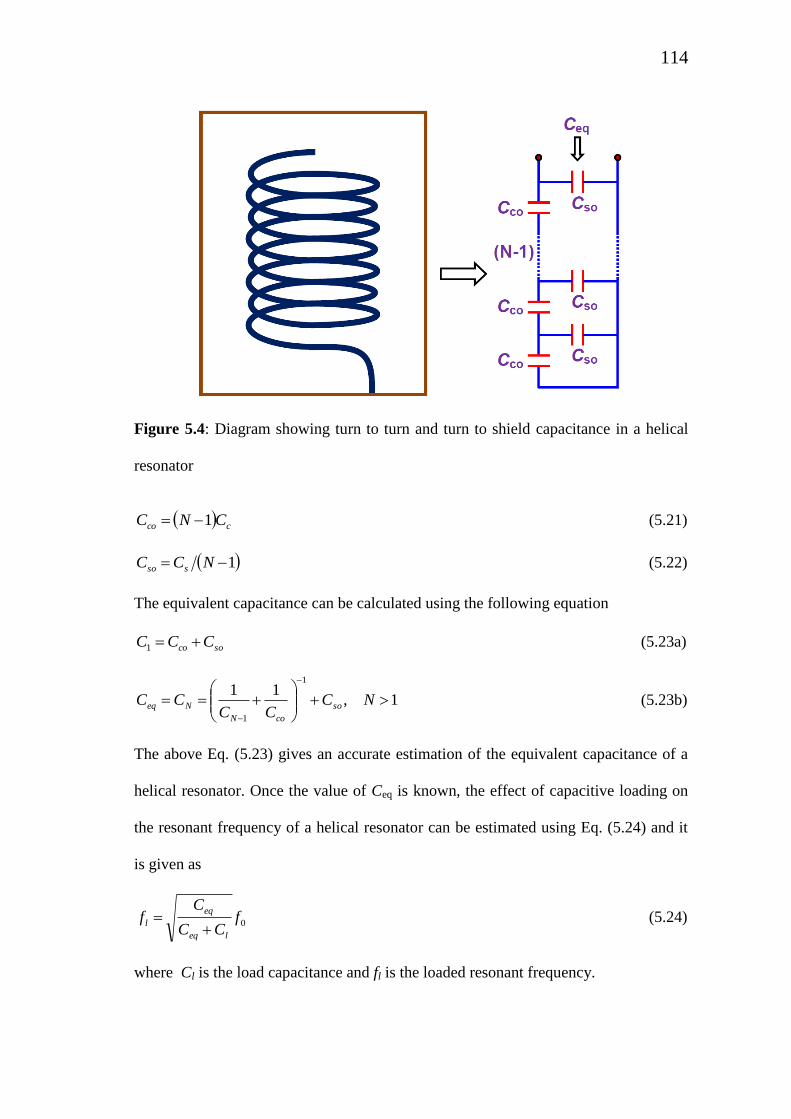
114
Figure 5.4: Diagram showing turn to turn and turn to shield capacitance in a helical
resonator
cco CNC 1 (5.21)
1 NCC sso (5.22)
The equivalent capacitance can be calculated using the following equation
soco CCC 1 (5.23a)
1,11
1
1
NCCC
CC so
coN
Neq (5.23b)
The above Eq. (5.23) gives an accurate estimation of the equivalent capacitance of a
helical resonator. Once the value of Ceq is known, the effect of capacitive loading on
the resonant frequency of a helical resonator can be estimated using Eq. (5.24) and it
is given as
0fCC
Cf
leq
eq
l
(5.24)
where Cl is the load capacitance and fl is the loaded resonant frequency.

115
5.3.3 Theoretical design
The capacitive loading due to trap electrodes, amplifier and associated cabling is
measured using the capacitance measurement schemes described in Chapter-4 and it is
observed that the overall system capacitance, which will affect the resonator is ~ 15
pF. Therefore the parameters of helical resonator should be chosen in such a way so
that with the above mentioned capacitive load, the loaded resonant frequency drops
down to a value between 60 – 70 MHz. In order to fix the design frequency, the
loaded resonant frequency with 15 pF load capacitance has been calculated for helical
resonator with different f0 and it is given in Table 5.1. It is clearly evident from Table
5.1 that an unloaded resonant frequency of 160 MHz drops down to 65.7 MHz, if
loaded with a 15 pF capacitive load. Therefore, a resonator with an unloaded resonant
frequency of 160 MHz is selected as a design frequency. The geometrical parameters
of the helical resonator at 160 MHz are calculated using Eq. (5.14) to Eq. (5.19) and
are tabulated in Table 5.2.
Table 5.1: Effect of 15pF load capacitance on helical resonator with different f0
f0
(MHZ)
Ceq
(pF)
Cl
(pF)
fl
(MHZ)
100 2.82 15 39.8
120 2.90 15 48.3
140 2.96 15 56.8
160 3.04 15 65.7
180 3.14 15 74.9

116
Table 5.2: Design parameters of 160 MHz helical resonator
Design Parameters Values
Outer shield diameter (D) 1.97 inches
Helix diameter (d) 1.08 inches
Helix length (b) 1.63 inches
Outer shield height (L) 2.61 inches
Helix wire diameter (d0) 0.12 inches
Number of turns (N) 6
5.4 HFSS simulation and fabrication
ANSYS HFSS [110] is a 3D full-wave electromagnetic structure simulation
software based on finite element method (FEM) which is widely used for the design
and analysis of various complex RF structures including antennas, filters, resonators
and for EMC/EMI study. Model of the helical resonator with the geometrical
parameters given in Table 5.2 is simulated using the Eigen mode solver in HFSS
software. A 3D model of the helical resonator is shown in figure 5.5. The model of
helical resonator is created by subtracting the helix winding from the outer cylindrical
shield using Boolean operation to realize a resonant cavity structure. In order to
provide the mechanical stability of the resonator geometry, a Teflon core will be used
to support the helix winding in actual design. Therefore we have also included a
hollow Teflon cylinder in the HFSS model of helical resonator. The effect of different
wall thickness of Teflon core on the resonant frequency of helical resonator is
simulated and it is illustrated in Table 5.3. It is clearly evident from Table 5.3 that the
wall thickness of the Teflon core should be kept very small to reduce the loading

117
Figure 5.5: Model of helical resonator in HFSS
Table 5.3: Effect of Teflon wall thickness on resonant frequency of helical resonator
Wall thickness (mm) f0 (MHz)
10 158.96
8 159.17
6 159.63
4 160.28
2.5 161.10
0 164.00
effect from dielectric material. The outer surface of the Teflon cylinder is grooved at
the position of helix winding to support the coil. The groove depth is kept as 1 mm
which is sufficient to hold the coil with wire diameter of 3 mm. This permits us to

118
choose the wall thickness of 2.5 mm for actual design, which otherwise will reduce
the mechanical strength of Teflon core for lower values of wall thickness. With this
geometry, an unloaded resonant frequency of 161.1 MHz with an unloaded Q of ~
1500 is obtained in simulation.
5.4.1 Simulation of capacitively loaded helical resonator
The effect of capacitive load on the resonant frequency of helical resonator is also
studied in HFSS and the simulated results are compared with the theoretical prediction
outlined in Section 5.3.2. The effect of capacitive load is simulated in HFSS by
extending the open end of the helix wire upto the upper surface of the outer cylindrical
shield and defining a lumped capacitive boundary on that surface as shown in figure
5.6. The simulated and estimated loaded resonant frequency with different capacitive
load is illustrated in Table 5.4.
Figure 5.6: Model of a capacitively loaded helical resonator in HFSS

119
Table 5.4: Estimated and simulated resonant frequency with different capacitive load
Capacitive load (pF) Loaded resonant frequency (MHz)
Estimated Simulated
1.8 122.96 123.26
4.7 97.25 97.19
6.8 86.25 86.20
8.2 80.70 80.66
10 74.93 74.75
12 69.77 69.49
15 63.71 63.44
20 56.37 56.02
5.4.2 Fabrication and testing with different capacitive load
The fabricated helical resonator along with a 2.5 mm thick Teflon core to support
the helix winding is shown in figure 5.7. The resonant frequency and Q of the
resonator is evaluated by sweeping the frequency of an RF source and measuring the
frequency response on a spectrum analyzer. The input and output signals are
capacitively coupled using the input and output port (designated as “5” and “6” in
figure 5.7). Unloaded resonant frequencies of 155.11 MHz with a Q of 1231 were
obtained. The effect of capacitive loading is studied by connecting one end of the
capacitor with the open end of the helix whereas the other end is connected with the
outer shield as shown in figure 5.8. A high Q SMD capacitor from Johanson
Technology is used for this purpose. The variation of resonant frequency and Q of the
resonator with different values of capacitive load is shown in figure 5.9. It is observed

120
Figure 5.7: Fabricated helical resonator; 1: Outer cylinder, 2: Helix winding, 3:
Bottom cover, 4: Top cover, 5: Input port, 6: Output port
Figure 5.8: Schematic setup for testing the helical resonator with capacitive load

121
Figure 5.9: Variation of resonant frequency and Q with different load capacitance.
that the loaded resonant frequencies in the case of estimated, simulated and
experimental results are in good agreement with each other within ~ 3 MHz. The Q of
the resonator for different capacitive load is estimated using Eq. (5.25).
0f
fQQ l
ul (5.25)
The difference between the estimated and experimental Q is due to the finite Q of the
capacitors used as well as the losses associated with the connection joints.

122
5.5 Summary
In this chapter, the design and implementation of a quarter wave helical resonator
is presented. The effect of capacitive load on the resonant frequency of a helical
resonator is studied with the help of theoretical model, finite element simulation and
experimental measurements. The model of a capacitively loaded helical resonator is
simulated in Ansys HFSS software. The simulation results are found to be very close
to the theoretical estimation. The resonator is fabricated and tested with different
values of capacitive load in the range of (1.8-20) pF. The experimental results are
found to be in good agreement with the theoretical and simulation results within ~ 3
MHz.

123
Chapter-6
Trapping and detection of electrons in
VECC Penning ion trap
6.1 Introduction
The design, development and characterization of the various indigenously built
electronic circuits for detection of trapped electrons has been discussed in previous
chapters. In this chapter, the arrangement made for trapping of electron cloud and
detection of the same using the detection circuit developed has been described. The
VECC PIT facility consists of five electrode flat endcap PIT assembly enclosed within
a 0.2 T annular ring magnet, FEP electron source and the detection circuit placed
within a vacuum chamber. In this facility, cloud of electrons is trapped and its axial
motion is detected using RF resonance absorption method.
In this chapter, we have presented the PIT facility at VECC for trapping cloud of
electrons and the test results of the detected axial signal. The chapter is organized as
follows: The complete assembly of the PIT facility is described in Section 6.2 whereas
Section 6.3 presents the schematic as well as coupled performance of the complete
detection circuit. The detailed test results of the detected absorption signal from
trapped electrons with different operating conditions are also presented in Section 6.3.
Finally, the chapter is summarized in Section 6.4.
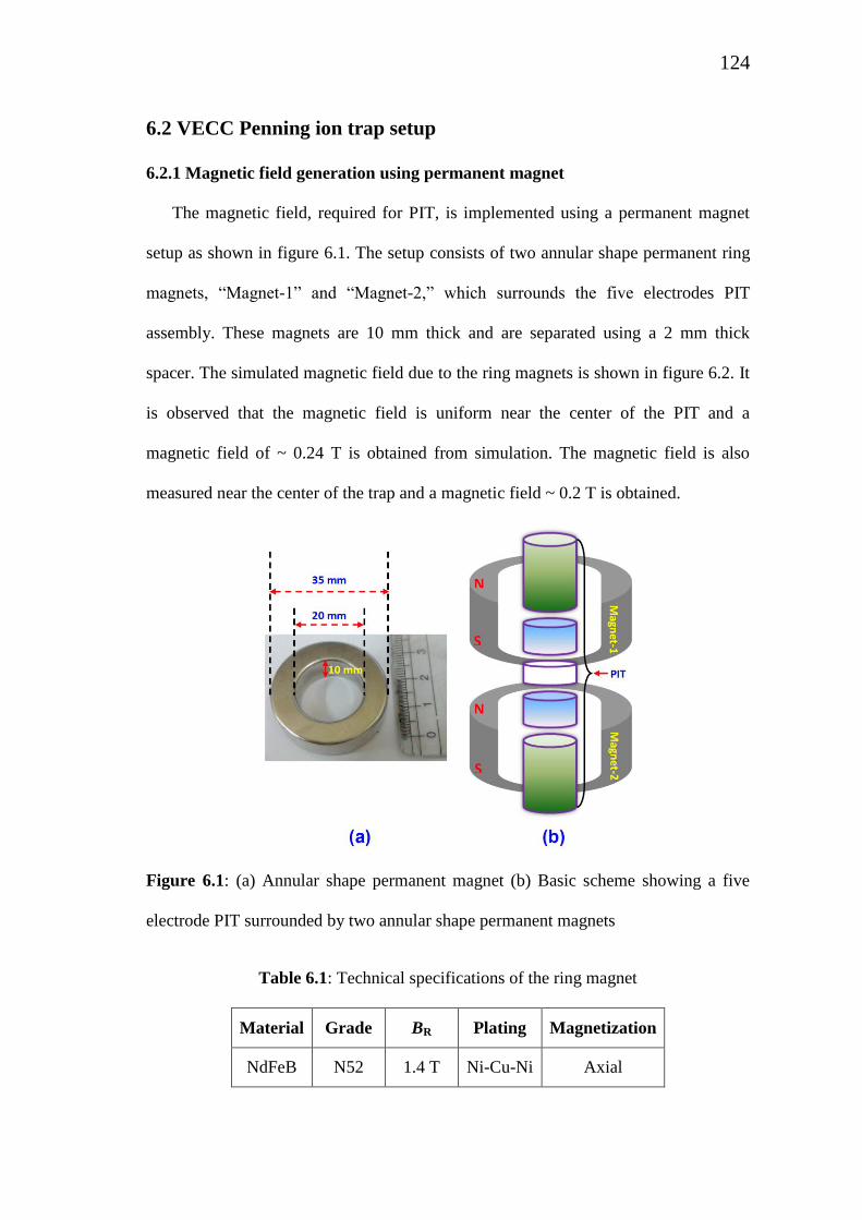
124
6.2 VECC Penning ion trap setup
6.2.1 Magnetic field generation using permanent magnet
The magnetic field, required for PIT, is implemented using a permanent magnet
setup as shown in figure 6.1. The setup consists of two annular shape permanent ring
magnets, “Magnet-1” and “Magnet-2,” which surrounds the five electrodes PIT
assembly. These magnets are 10 mm thick and are separated using a 2 mm thick
spacer. The simulated magnetic field due to the ring magnets is shown in figure 6.2. It
is observed that the magnetic field is uniform near the center of the PIT and a
magnetic field of ~ 0.24 T is obtained from simulation. The magnetic field is also
measured near the center of the trap and a magnetic field ~ 0.2 T is obtained.
Figure 6.1: (a) Annular shape permanent magnet (b) Basic scheme showing a five
electrode PIT surrounded by two annular shape permanent magnets
Table 6.1: Technical specifications of the ring magnet
Material Grade BR Plating Magnetization
NdFeB N52 1.4 T Ni-Cu-Ni Axial

125
Figure 6.2: Simulated magnetic field along the trap axis
6.2.2 Five electrode flat endcap cylindrical Penning ion trap electrodes
In this PIT facility, quadrupolar electric field is generated by applying potentials to
the five electrode cylindrical PIT with flat endcap electrodes [111] as shown in figure
6.3. Here, different electrodes of the PIT are separated from each other using a
MACOR dielectric. The simulated harmonic potential for the PIT assembly is also
plotted in figure 6.3, which shows a harmonic region of 4.4 mm around the center of
the PIT. A small hole of 2 mm diameter is made on the endcap electrodes for loading
and ejecting the electrons.
6.2.3 Setup for generation of electrons
Two well known methods for generation of electrons from the metal surface are
thermionic emission and field emission. In a thermionic emission process, a filament
is heated using a power source (usually a constant current source as described in
Appendix – A). The heating process increases the kinetic energy to a sufficient value

126
Figure 6.3: Basic schematic of a five electrode flat endcap cylindrical PIT. Here the
electrodes abbreviations are defined as, UE: Upper Endcap, UC: Upper
Compensation, R: Ring, LC: Lower Compensation, LE: Lower Endcap
which results in emission of electrons from the filament surface. An additional
extraction electrode is also used to accelerate the electron beam to a given kinetic
energy. In a field emission process, a very strong electric field is applied between a
metallic tip and a metallic surface, placed close to the tip. The electrons in the metallic
tip (~ few microns diameter) experience a force due to the electric field which results
in emission of electron from the metal tip.
In VECC PIT facility, electrons are generated by field emission process (FEP).
The basic schematic of the setup for electron generation using FEP is shown in figure
6.4. In this method, a sharp tungsten wire with a tip diameter ~ 1 – 2 microns is used
for generation of electrons. An electric field, E, is applied at the tungsten tip which
results in the emission of electrons with an emission current EBeAE 2
, A and B are
universal constants [112]. The electrons emitted from the tip are directed into the PIT
region via a 0.2 mm hole made on the “Cu Bias” electrode. These high energy

127
Figure 6.4: Schematic setup for electron generation using FEP
electrons create secondary electrons on colliding with gas molecules and trap
electrodes. In this PIT facility, these low energy secondary electrons are trapped by
applying the required voltages to the PIT electrodes. It was observed that the
threshold voltage required to observe a current at the Cu-bias or at the faraday cup
depend on the position of the tip with respect to the Cu-bias electrode. A typical
current, required to observe signal from PIT, is around 10 nA at the faraday cup and it
is obtained when a voltage of -1 kV to -3 kV is applied at the FEP tip with Cu-bias
electrode kept at ground potential.
6.2.4 Cabling and assembly of Penning ion trap facility
The complete PIT facility along with the cabling of PIT electrodes with various
electronic modules is shown in figure 6.5. The assembled setup is supported by three
copper rods which are mounted on to the top flange as shown in figure 6.5 (a). All the
electrical connections are routed through indigenously developed cryogenic vacuum
feedthrough which is made using an epoxy material (STYCAST 2850 FT blue). The
feedthrough consists of 19 single pins, which are used for transmitting various dc
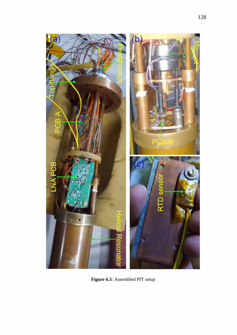
128
Figure 6.5: Assembled PIT setup

129
potentials, and 3 coaxial pins for transmission of RF signals. The required dc
potentials on the different electrodes of PIT are filtered using low pass RC circuits,
implemented on a circuit board “PCB-A”. Arrangement of the magnet pairs
surrounding the ion trap electrodes are shown in figure 6.5 (b). Here the circuit board
“PCB-B” is used to connect the trap electrodes with the detection circuit (Helical
resonator and LNA). An RTD sensor is mounted on the back side of the LNA (Figure
6.5.c) for monitoring the temperature during cryogenic testing. The detailed schematic
of the electrical connections are discussed in Section 6.3.
6.2.5 Ultra high vacuum setup
For trapping and detection of electrons at room temperature, an ultra high vacuum
(UHV) setup has been assembled as shown in figure 6.6. An indium vacuum sealing,
which is compatible with cryogenic operation, is used between the top flange of the
PIT assembly and the vacuum setup. The pumping of the setup is done using an ion
pump coupled with a turbo molecular pump. During pumping of the setup, both the
gate valves (Gate valve-1 and Gate valve-2) is kept open and pumping of the setup is
performed using the turbo pump to reduce the pressure below 6101 mbar. Once the
pressure reduces below 6101 mbar, the ion pump is turned on to further reduce the
pressure. More detailed procedure for operating an ion pump is given in [113]. With
the help of the ion pump the ultimate vacuum of ~ 7109.1 mbar is obtained.

130
Figure 6.6: Ultra high vacuum setup for PIT
6.3 Experimental testing and results
The complete circuit schematic for the detection of axial motion of trapped
electrons is shown in figure 6.7. The DC voltages, required for generating quadrupolar
field within the PIT, are filtered using first order low pass RC circuits. These low pass

131
Figure 6.7: Detailed circuit schematic for detection of trapped electrons
filtering circuit is implemented on a circuit board “PCB-A”. An external RF drive is
weakly coupled with the tank circuit to excite the amplitude of oscillation of the
trapped electrons. The output of the tank circuit, connected with the LE electrode of
the PIT, is capacitively coupled with the LNA for necessary amplification. The
amplified signal from the trapped electron is downconverted to a DC or intermediate
frequency with a mixer and the downconverted signal is filtered using an LPF. Finally
the filtered output is observed on an oscilloscope (Tektronix MDO-3034). For signal
acquisition and further processing, trapped electron signal is acquired using a data
acquisition card (PCI-4472) interfaced with LabVIEW software.
6.3.1 Performance test of the detection circuit without trapped electrons
The performance of the detection circuit is evaluated by calculating the resonant
frequency and Q from the measured frequency response of the detection circuit. The
frequency response is measured by sweeping the frequency of a signal generator in the
range of 60 MHz – 62 MHz in steps of 10 KHz and recording the output power of

132
Figure 6.8: Frequency response of the detection circuit for Id1 = 1 mA
the detection circuit using the RF port of a tektronix oscilloscope (MDO – 3034).
Initially, the output of the tank circuit, connected with the LE electrode of the PIT, is
directly coupled with the LNA which results in a very low Q ~ 45. In order to reduce
the loading effect from the LNA, a very low value coupling capacitor of 4.7 pF is used
to improve the Q of the detection circuit. A typical frequency response of the
detection circuit with an input RF drive power of -20 dBm is shown in figure 6.8. A
loaded Q of 115 is obtained at a resonant frequency of 60.97 MHz. The variation of
the resonant frequency and Q for different operating current Id1 of the LNA is listed in
table 6.2. It is observed that the resonant frequency slightly shifted from 60.97 MHz to
Table 6.2: Variation of resonant frequency and Q with Id1
Id1 (mA) 1 2 3 4 5
f0 (MHz) 60.97 60.91 60.87 60.87 60.85
Q 115 121 124 127 132

133
60.85 MHz for variation of Id1 from 1 mA to 5 mA. The Q of the detection circuit also
improves by a factor of 1.15 for an increase in Id1 from 1 mA to 5 mA.
6.3.2 Detection of trapped electrons at room temperature
In this PIT facility, the secondary electrons, generated due to the collision of
primary electrons beam from the FEP (refer Section 6.2.3 ) with the background
gases, are trapped and the absorption signal from the trapped electrons is detected
using the narrowband detection circuit shown in figure 6.7. The DC quadrupolar field
is generated by applying the potentials UE and UC-R on the trap electrodes as shown in
figure 6.7. Here we have applied the same potentials on the compensation (UC and
LC) and ring electrode. The potential difference U0 between the endcap (UE and LE)
and ring electrode can be written as,
RCE UUU 0 (6.1)
The trapped electrons are weakly excited using an external RF source whose
frequency is always kept in resonance with the detection circuit. A ramp voltage
(UC-R: 0V to -10V) is applied on both the ring and compensation electrodes whereas
the endcap electrode is subjected to a fixed DC voltage (UE). The trap voltage is thus
swept over a specified range. By sweeping the trap potential U0, trapped electrons
absorbs the energy from the tank circuit at a particular value of U0 when the resonant
frequency of the detection circuit coincides with the electron‟s axial frequency (as
described in Section 2.4.2.c). The absorption signal due to trapped electrons is then
downconverted to a DC signal. A typical absorption signal of trapped electrons, as
observed in the oscilloscope, is shown in figure 6.9. Here LNA is operated at Id1 = 3
mA. It is seen from figure 6.9 that absorption signal has been observed at the same

134
Figure 6.9: Oscilloscope snapshot of the absorption signal from trapped electron
trap potential (UC-R ≈ -4.3V; U0 ≈ -11.7V) on both the cycle of the ramping voltage as
expected for detection based on RF absorption method. The downconverted signal is
also acquired and processed using a data acquisition card (PCI-4472) interfaced with
LabVIEW software. The block diagram of the LabVIEW acquisition system is shown
in figure 6.10. Here, three analog input channels of the PCI-4472 are configured to
acquire three different parameters: absorption signal from trapped electrons, ramp
voltage (UC-R) and current on Cu bias electrode. The three channels are then separated
and observed in the LabVIEW front panel as shown in figure 6.11. These three
channels are also acquired for further analysis and processing. The LabVIEW
acquisition is kept running on a continuous mode while the absorption signal in 35
different ramp cycles is acquired. It is seen that the magnitude of the dip in signal as
well as the ramp voltage at which it is observed varies each time the experiment is
repeated as shown in figure 6.12. The signal is observed at different ramp voltages in
the range of -3.8V to -4.7V (figure 6.12). This could be attributed to space charge
effects and other imperfections in the trap. However, the magnitude of the dip signal
reduces below 8 mV for UC-R > -4.1V and the dip voltage magnitude lies between

135
Figure 6.10: Block diagram of data acquisition in LabVIEW
Figure 6.11: Front panel of data acquisition in LabVIEW

136
Figure 6.12: Typical distribution showing the dip observed at different ramp voltage
Figure 6.13: The absorption signal from trapped electrons

137
8mV – 8.5mV for UC-R in the range of -4.1V to -4.7V. A maximum dip voltage ~
8.5mV occurs for UC-R ~ -4.3V. A typical absorption signal from the trapped
electrons, excited with an RF drive power of -20 dBm, is plotted in figure 6.13. The
LNA is operating at a drain current Id1 of 1mA. The panel (b) of this figure shows the
voltage dip in the downconverted IF signal of 5 KHz. For ease of understanding and
visibility, the absorption signal is downconverted to a DC signal as shown in the panel
(c) of figure 6.13. The absorption signal for the downconverted 5 KHz IF signal as
well as DC signal has been observed for a trap voltage, U0, ~ -11.68V. The magnitude
of the dip in the downconverted DC signal is found to be ~ 8.5 mV. The variation in
trapped electron signal under different conditions is described below.
(a) Effect of endcap voltage (UE) on the absorption signal from trapped electrons
The position of absorption signal with respect to the sweeping potential UC-R depends
on the voltage applied on the endcap electrodes. If the potential on the endcap
electrode is switched to a different value, the position of the absorption signal is also
expected to shift accordingly to maintain a fixed trapping potential U0. Figure 6.14
shows the shift in the absorption signal having maximum dip magnitude for different
voltages applied on the endcap electrode. It is observed that the position of the
absorption signal shifted by almost 1V for a unit change in the voltage on endcap
electrodes.
(b) Effect of excitation power on the absorption signal from trapped electrons
The absorption signal is acquired for different RF excitation power in the range of
-10 dBm to -60 dBm to see its effect on the magnitude of the dip signal. A typical
variation of the magnitude of absorption signal for different RF excitation power is

138
Figure 6.14: Shift in absorption signal due to different voltages applied on the endcap
electrodes. Trapping conditions: RF drive power = -20 dBm, Id1 = 1 mA
shown in figure 6.15. It can be seen from the plot that the magnitude of the absorption
signal increases with an increase in RF drive power from -60 dBm to -15 dBm. This
shows that the amplitude of oscillation of the excited trapped electrons depends on the
RF energy supplied to the tank circuit. However, further increase in the RF drive
power above -10 dBm causes disappearance of the absorption signal. This mainly
happens due to the large oscillation amplitude of trapped electrons for higher RF drive
power which results into collision with trap surfaces. The magnitude of absorption
signal for different RF excitation power is listed in table 6.3.

139
Figure 6.15: Effect of different excitation power on the magnitude of absorption
signal. Trapping conditions: Id1 = 1 mA
Table 6.3: Magnitude of absorption signal for different RF excitation power
RF drive
(dBm)
Absorption signal
(mV)
Trapping potential, U0
(V)
-15 10.52 -4.43
-20 8.49 -4.33
-30 2.28 -4.6
-40 0.85 -4.32
-50 0.47 -4.39
-60 0.35 -4.32
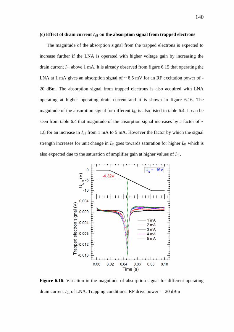
140
(c) Effect of drain current Id1 on the absorption signal from trapped electrons
The magnitude of the absorption signal from the trapped electrons is expected to
increase further if the LNA is operated with higher voltage gain by increasing the
drain current Id1 above 1 mA. It is already observed from figure 6.15 that operating the
LNA at 1 mA gives an absorption signal of ~ 8.5 mV for an RF excitation power of -
20 dBm. The absorption signal from trapped electrons is also acquired with LNA
operating at higher operating drain current and it is shown in figure 6.16. The
magnitude of the absorption signal for different Id1 is also listed in table 6.4. It can be
seen from table 6.4 that magnitude of the absorption signal increases by a factor of ~
1.8 for an increase in Id1 from 1 mA to 5 mA. However the factor by which the signal
strength increases for unit change in Id1 goes towards saturation for higher Id1 which is
also expected due to the saturation of amplifier gain at higher values of Id1.
Figure 6.16: Variation in the magnitude of absorption signal for different operating
drain current Id1 of LNA. Trapping conditions: RF drive power = -20 dBm

141
Table 6.4: Magnitude of absorption signal for different Id1
Id1 (mA) 1 2 3 4 5
Absorption
signal (mV)
8.49 11.60 13.42 14.47 15.00
6.3.3 Detection of trapped electrons at 100K
In order to test the cryogenic performance of the detection circuit with trapped
electrons, an open ended cylindrical housing is mounted with the setup as shown in
figure 6.17. Cryogenic vacuum grease is used in between the cylindrical housing and
Figure 6.17: Arrangement for operating the PIT at cryogenic temperature

142
support flange to stop the leakage of cryogen (here LN2). To cool the PIT setup within
the vacuum chamber, LN2 is filled within the cylindrical housing which helps to
achieve a cryogenic temperature of ~ 100K, measured at the location of LNA board,
within a period of 2 – 3 hours. The vacuum within the chamber also reduces to a value
of ~ 9108.6 mbar at cryogenic temperature. The measured results of absorption
signal from trapped electrons for operating drain current of 0.5 mA and 1.0 mA is
shown in figure 6.18. It is observed that the trapping potential U0, at which the energy
is absorbed by trapped electrons, shifted to a value of -9.63V at 100K as compared to
-11.68V at room temperature. This clearly indicates that there is significant change in
the trapping condition at cryogenic temperature. Also the magnitude of the absorption
Figure 6.18: Absorption signal for different operating drain current Id1 of LNA at a
cryogenic temperature of 100K. Trapping conditions: RF drive power = -30 dBm
143
signal reduces to ~ 1.72 mV at 100K. This happens due to the lower number of
secondary electrons generated due to high vacuum condition at cryogenic temperature.
6.3.4 Testing of Colpitts oscillator to excite and detect the electrons
Measured results of absorption signal presented in Section 6.3.2 and Section 6.3.3
uses an external arbitrary function generator from Tektronix (AFG-3102) to excite the
motional amplitude of trapped electrons. We have also tested our designed Colpitts
oscillator to provide the required RF energy to excite the trapped electrons. The
schematic block diagram for generating an RF drive power of -20 dBm is shown in
figure 6.19. The first stage of the Colpitts oscillator module (refer to figure 4.1) is
powered by a 10V DC source to increase the RF power level to -7 dBm. The output of
the Colpitts oscillator is then attenuated to -17 dBm using a 10 dB attenuator. The
attenuated signal is then splitted into two components using a 3-dB power splitter. The
first component provides the required RF power of -20 dBm, which are used to excite
the amplitude of trapped electrons. The LO power required for downconversion is also
derived using Colpitts oscillator by amplifying the second component of the power
splitter, which provides a 0 dBm drive for the LO port of the mixer. Finally the
downconverted signal is acquired and processed in LabVIEW. The frequency of the
Colpitts oscillator is always kept in resonance with the tank circuit using a tuning
capacitor. The trapped electrons are excited using Colpitts oscillator and the
absorption signal from trapped electron is acquired as shown in figure 6.20. The
magnitude and the position of the absorption signal in case of both the signal source
(signal generator and Colpitts oscillator) is found to be in good agreement with each
other.

144
Figure 6.19: Block diagram of RF drive system using Colpitts oscillator
Figure 6.20: Excitation and detection of absorption signal using standard signal
generator and Colpitts oscillator. Trapping conditions: RF drive power = -20 dBm, Id1
= 1 mA

145
6.4 Summary
This chapter describes in detail the PIT setup operating at room temperature and at
a cryogenic temperature of 100K.The electron cloud trapped in the VECC PIT was
detected and signal was observed using the narrow band detection circuit developed.
The performance of the detection circuit based on resonant technique was reasonably
good with a Q value of ~130. Under varied conditions detection circuit detected
trapped electron signal and different trapping parameters could be studied. The
performance of the detection circuit was satisfactory at cryogenic temperature and
trapped electrons cloud signal was successfully detected at cryogenic temperature of
100 K. Apart from the trapping and detection of electrons, an indigenously developed
RF energy source (Colpitts oscillator) is also successfully operated and excited the
motional amplitude of trapped particles. Performance of the indigenously developed
RF energy source and standard signal source from Tektronix is in reasonable
agreement.

146
Chapter-7
Conclusion and future outlook
7.1 Conclusion
In this thesis, the key technical issues and challenges related with the design and
implementation of low noise detection circuit for charged particle detection in a PIT is
discussed. The low noise detection circuit, composed of a high Q helical resonator and
an LNA, along with a stable low distortion Colpitts oscillator, which supply the
required RF energy to excite the trapped particle, is indigenously developed and their
detailed characterization and test results are presented. Cloud of electrons is trapped in
a PIT facility and the results of detected axial signal are summarized in this thesis.
Detection of axial signal of trapped electrons (~ 63 MHz) requires an LNA with
sufficiently high bandwidth to get maximum amplification of the signal. In this thesis,
we have discussed various bandwidth enhancement techniques and presented the
design of an inductively tuned common source LNA. Here, the limitation in the
theoretical model of the amplifier with shunt peaking technique is investigated and an
improved model, that includes the effect of rd on the BWEF of the amplifier, is
presented. The predictions of the proposed model showed that the maximum BWEF
of 1.72, as given by Mohan et al., is achievable only for the case of Rrd .
However, in the case of Rrd , the maximum BWEF of the amplifier reduces below
∼1.45. The amplifier is implemented on a Teflon substrate and its frequency response
is measured as a function of load inductance and operating drain current. With a load
inductance of 1 μH, a 3-dB bandwidth of ~ 132 MHz is obtained for Id1 = 1 mA, and

147
the bandwidth further increases to ~ 194 MHz for Id1 = 5 mA. The effect of dielectric
material on the performance of the amplifier is also investigated and it is observed that
the bandwidth of the amplifier, implemented in an FR4 substrate, reduces by a factor
of ~ 1.5 as compared to that obtained in a Teflon substrate. The amplifier is also
successfully tested at a cryogenic temperature of 130K and improved performance in
terms of voltage gain as well as input voltage noise density of the amplifier has been
observed. Cooling the LNA to 130K increases the voltage gain from 4.3 at room
temperature to 6.5 at 130K. The input voltage noise density also improves from
HznV6.2 at room temperature to HznV5.1 at 130K.
The capacitance of the PIT assembly contributes a significant figure in the overall
system capacitance and therefore, its measurement is required for the design of a high
Q tank circuit. In this thesis, a high frequency Colpitts oscillator, operating in the
vicinity of electron‟s axial frequency (~ 63 MHz), is designed and implemented for in-
situ capacitance measurement of PIT assembly. One of the key motivations in making
such an in-situ arrangement is to measure the PIT assembly capacitance placed within
the vacuum chamber. The capacitance measurement for a series of standard SMD
capacitor in the range of (0.5 – 3.3) pF is carried out using Colpitts oscillator and the
measured results are compared with that obtained using a standard impedance
analyzer. The measured result using both the techniques agrees well within ~ 0.05 pF.
The key performance indices like, for instance, amplitude and frequency stability,
warm-up and response time, accuracy and standard deviation, sensitivity, resolution
and repeatability of the Colpitts oscillator are investigated based on the experimental
results. The capacitance of the PIT assembly is also measured using Colpitts oscillator
and the measured capacitance is in good agreement with that obtained using another

148
alternate resonance based technique, implemented using helical resonator. In addition
to the in-situ capacitance measurement, the same Colpitts oscillator, integrated with
frequency tuning arrangement, is used to excite the trapped particles at a given
frequency during detection process.
A high Q resonant circuit is implemented using a quarter wave helical resonator.
Based on the measurements of different capacitive load that will contribute to the
detection system, several helical resonators and their resonant frequency for the given
load capacitance (~ 15 pF) is theoretically studied. Based on the theoretical
estimation, it is observed that a 160 MHz helical resonator with a 15 pF capacitive
load reaches to a resonant frequency of 65.7 MHz, which is in the vicinity of the axial
frequency of electrons (~ 63 MHz). We have also established a simulation approach
and studied the performance of a capacitively loaded helical resonator in ANSYS
HFSS. The effect of Teflon core on the performance of helical resonator is also
studied in the simulation. Finally the resonator with a Teflon core thickness of 2.5 mm
is fabricated and the effect of different load capacitance on the resonant frequency of
helical resonator is experimentally studied. The experimental results are found to be in
good agreement with the theoretical and simulation results within ~ 3 MHz.
Finally, the prototype PIT facility, operating at room temperature and at a
cryogenic temperature of 100K, is described in detail. In this facility, electron clouds
are trapped and their axial signal is detected using the indigenously developed
detection circuit. Initially a low Q value ~ 45 at a resonant frequency of 56.57 MHz is
obtained. The Q of the detection circuit is further improved by isolating the tank
circuit and LNA with a 4.7 pF coupling capacitor. This reduces the loading effect
from LNA and helps in achieving a Q value of ~ 115 at a resonant frequency of 60.97

149
MHz. The axial signal due to trapped electrons is detected using RF resonance
absorption method and the effect of various trap parameters on the detected absorption
signal are studied. It is observed that a very low RF drive power (less than -40 dBm) is
unable to excite the trapped electrons, which leads to difficulty in detecting the
absorption signal. Also it is not preferable to use much larger RF drive power (~ -10
dBm or higher), which leads to loss of trapped electrons due to collision with trap
electrodes. The detection circuit is also able to detect the absorption signal from
trapped electrons when the PIT facility is operated at a cryogenic temperature of
100K. However it is found that the trapping potential shifts from -11.68V at room
temperature to -9.63V at 100K. We have also tested the Colpitts oscillator‟s
performance in exciting the motional amplitude of trapped electrons and the results
are in close agreement with that obtained using a standard signal generator.
7.2 Future prospect
The work reported in this thesis made an attempt to highlight the key technical
challenges and their remedies related with the design and development of low noise
detection circuit for PIT. However, there are still some additional issues and
improvements which will be explored in the near future.
With an inductive shunt peaking technique implemented in a common source
amplifier, a BWEF of ~ 1.45 has been achieved. One could further enhance the
bandwidth by a factor of ~ 3 or even more using a shunt-series peaking technique.
However, more theoretical work has to be carried out to investigate the effect of drain-
source resistance on the BWEF of an amplifier for shunt-series peaking technique.
Bandwidth enhancement in an amplifier could also be achieved by using an ac
boosting amplifier after the main amplification stage [114]. In [114], a dual op-amp

150
along with a combination of R-C network is used to enhance the bandwidth by
boosting the gain of the first stage. One of the advantages of this technique is that it
offers an inductor free amplifier design and therefore it could give better results for
high frequency amplifier design in near future. In this thesis, cryogenic performance
of the LNA has been tested up to a temperature of 130K. Further experimental testing
and detailed characterization of the LNA at 4K will be taken up in near future. The
detailed experimental studies of BWEF with the variation in load inductance and
operating drain current will be also investigated at cryogenic temperature.
Additionally, the input voltage noise density of the LNA at room temperature is ~
HznV2 and it increases above HznV4 below 1 MHz due to the presence of
flicker noise, which limit its operation at low frequency region. One could reduce the
contribution of flicker noise by implementing a cascode amplifier with FET having
low flicker corner frequency. Additionally noise could also be reduced by paralleling
two identical FETs as reported in [58]. Such design improvement of the LNA will be
carried out to reduce the thermal and flicker noise of the amplifier so that it could be
useful for detection of the image signal from heavy ions in near future.
Trapping of electron clouds and the results of detected absorption signal are
presented in Chapter – 6. The Q of the coupled circuit, which is used to detect the
electron‟s axial signal, is ~ 115 and it will be further improved by optimizing the
coupling between the helical resonator and LNA. More detailed analysis of the
detected absorption signal needs to be carried out to understand the behavior of
trapped electrons. The number of electrons that are trapped in the PIT will also be
estimated using the detected absorption signal. Furthermore, a Colpitts oscillator is
developed and it is used to excite the trapped electrons as illustrated in Section 6.3.4.

151
Here the Colpitts oscillator is kept outside the vacuum chamber and the required RF
power is transmitted within the vacuum chamber through a feedthrough shown in
figure 6.5. In the near future, the two-fold applications of the Colpitts oscillator with
an in-situ circuit arrangement, as proposed in Section 4.6, will be implemented. The
required demodulation circuit for the detection of absorption signal will also be
implemented in-situ. This in-situ arrangement for generating RF excitation power and
demodulating the detected RF absorption signal will prohibit the requirement of long
RF transmission line. Therefore the demodulated output signal will not be affected by
the problems, which are generally encountered in an RF coaxial cable at high
frequency such as, attenuation and reflection loss, crosstalk, unwanted noise from
external environment, signal leakage, ground loop etc. Additionally, the in-situ
capacitance measurement arrangement will be used to study the capacitance of the PIT
electrodes with trapped charged particles, which may be very useful to study the
behavior of charged particles. Finally, the 4K cryogenic PIT facility, as described in
Section 2.5 will also be commissioned and our detection circuit will be used to detect
the trapped electrons.

152
Appendix-A
Constant current DC supply for
thermionic generation of electrons
In a thermionic emission process, electrons are generated by heating a filament
load (load resistance is usually less than 1 Ω) to a very high temperature using an
external power source. For this purpose, a current regulated 0–10A DC power supply
with a maximum output voltage of 5V has been designed and fabricated. In this
power supply, an LC filter followed by a current regulator based feedback control
scheme has been used to reduce the ripple in the load current [115]. The basic building
blocks of the power supply are shown in figure A.1. In this power supply, a current
sensor senses the load current and transforms this current into an equivalent output
voltage. The output voltage of the current sensor is then compared with a set voltage,
which is proportional to a given load current. The difference signal between the set
voltage and output voltage drives the controller circuit to generate a control signal
which regulates the current flowing through the load. The complete circuit schematic
of the DC power supply is shown in figure A.2. Here the rectified DC output of the
bridge rectifier is filtered using an LC filter to smooth out the fluctuations in the DC
load current. A bleeder resistor of 0.5 kΩ, in parallel with the filter
capacitor mFC 54 , is used to provide fast discharge of the electric charge stored
in the filter capacitor when the load is disconnected or the power supply is turned off.
In order to reduce the fluctuations in the DC load current, a current regulator has been

153
Figure A.1: Schematic block diagram of the DC power supply
Figure A.2: Circuit schematic of the current regulated DC power supply. Here dashed
line in the circuit schematic separates various functional modules of power supply

154
implemented using an insulated-gate bipolar transistor (IGBT) IRG4PH50UD [116].
In order to sense the fluctuations in DC load current, a DC current transformer
(DCCT), EL25P1 [117], with a turn ratio of 1:1000 is used. It senses the DC current
flowing through the load and gives an output current that is 1000 times lower as
compared to the primary load current. The output current of the DCCT is transformed
into a voltage signal by passing it through a 100 Ω resistor (implemented with a 47 Ω
fixed resistor in series with a 100 Ω variable resistor). The output voltage of the buffer
amplifier (implemented using an OPAMP, OP07) is then compared with a set voltage
(controlled by the 90 kΩ resistor along with the 10 kΩ variable resistor) and the
difference signal is then fed to the controller circuit, which is basically a differential
amplifier implemented using OP07. Finally, the output of the differential amplifier
generates a control voltage that commands the IGBT to regulate the current flowing
through the load. The assembled DC power supply is shown in figure A.3. Figure A.4
shows the typical load regulation performance of the power supply when the load
resistance is changed from 0.57 Ω to 0.07 Ω at a load current of 10A. Provision for
adjusting the higher current limit as well as protection against overload is also
incorporated in this power supply. The detailed technical specifications of the power
supply are given in Table A.1.
Figure A.3: Current regulated DC power supply
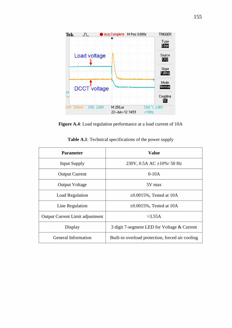
155
Figure A.4: Load regulation performance at a load current of 10A
Table A.1: Technical specifications of the power supply
Parameter Value
Input Supply 230V, 0.5A AC ±10%/ 50 Hz
Output Current 0-10A
Output Voltage 5V max
Load Regulation ±0.0015%, Tested at 10A
Line Regulation ±0.0015%, Tested at 10A
Output Current Limit adjustment >3.55A
Display 3 digit 7-segment LED for Voltage & Current
General Information Built-in overload protection, forced air cooling

156
Appendix-B
Measurement of trap capacitance at
cryogenic temperature
The capacitance of the PIT assembly has also been measured at cryogenic
temperature using the Colpitts oscillator circuit as described in Chapter-4. Accurate
measurement of capacitance of PIT assembly at high frequencies requires that both the
PIT assembly and the measurement circuit (Colpitts Oscillator) should be kept close to
each other to minimize the effects of stray capacitance and inductance. However, it
has been observed that the designed Colpitts oscillator fails to operate properly below
a temperature of 260 K due to the cryogenic compatibility issues of different active
and passive components used in the circuit. Therefore, capacitance measurement of
PIT assembly has been carried out in a specially designed cryogenic test setup with
two different temperature regions (Measurement Circuit at high temperature and trap
assembly at low temperature). The setup holding the PIT assembly and Colpitts
oscillator enclosed within an aluminium box is shown in figure B.1. The PIT assembly
is placed at the bottom of the holding assembly to measure its capacitance. Above the
PIT assembly, SS stand holds a square aluminum box containing a cartridge heater (25
W from Lakeshore), attached to an aluminum plate, and the measurement circuit
(Colpitts Oscillator). A 10 mm hole is also drilled in the Al Box for routing the cables
carrying different electrical signals. As the measurement circuit is designed on an FR4
Glass epoxy substrate, uniform heating of the circuit is not possible using conductive

157
Figure B.1: Setup holding assembly to facilitate capacitance measurement at
cryogenic temperature
heating. Therefore radiation heating mechanism was employed as it helps to achieve
uniform heating of the entire circuit board. The Colpitts oscillator circuit is maintained
at a fixed temperature of 290K during capacitance measurement of the PIT assembly.
In order to control the temperature of oscillator circuit at 290K, a Lakeshore
temperature controller is used. To minimize the effect of heat transfer from the higher
temperature side (Al Box) to the lower temperature side (PIT assembly), Al box is
insulated with 5 layers of multi layer insulation (MLI) sheets. Also an aluminium plate
wrapped with an aluminium foil is used as a reflecting surface and it is kept in
between higher and lower temperature region to minimize the heat transfer from one
side to the other. A Teflon insulated coaxial cable with copper as a central conductor
is used to connect the unknown capacitance slot in the Colpitts oscillator to the PIT
assembly via an FR4 PCB placed in between the reflecting surface and the PIT
assembly. This PCB contains different slots for connecting the trap electrode and the

158
Figure B.2: LabVIEW GUI for monitoring temperature and oscillation frequency
Figure B.3: Schematic of the setup holding the circuit enclosed in an insulated box
and PIT assembly within LN2 cryostat
coaxial cable. RTD sensors (PT-100) are mounted on Heater Plate, Colpitts oscillator
circuit PCB, lower PCB and one of the electrodes of PIT to monitor the temperature.
For continuous monitoring of different experimental parameters like oscillator
frequency and temperature at different points, a LabVIEW based data acquisition

159
system is developed as shown in figure B.2. The total holding assembly is kept inside
a SS cylinder that is placed within an open ended LN2 Dewar as shown in figure B.3.
The vacuum port, gas insertion port and electrical connection port are provided on the
top flange of the SS cylinder. A 19 pin electrical feedthrough, as shown in figure B.4,
has been fabricated on a G10 material where the pins are fixed using araldite adhesive.
This feedthrough is used for getting electrical signals from heater element,
temperature sensors and Colpitts oscillator circuit. Two PT-100 sensors are mounted
on a glass rod and kept in the LN2 chamber to monitor the level of LN2. First, the
innermost cylinder was evacuated to remove any moisture content. At the same time,
acquisition of different experimental parameters is started. After the evacuation
process, the LN2 chamber is filled with liquid nitrogen and heater for circuit heating is
switched on. After LN2 filling process, a cooling gas (Helium gas) is inserted in the
innermost cylinder at a controlled way and convective cooling of the setup holding
assembly begins. During the starting phase of He gas cooling, temperature of the
Colpitts oscillator fluctuates but it stabilizes at the set point temperature (Here, 290K)
within 40 minutes as seen in the top chart of figure B.5. The circuit remains stabilized
at 290±1K. As the temperature of the trap assembly and lower PCB decreases with
Figure B.4: 19-pin electrical feedthrough fabricated at VECC

160
Figure B.5: Cooling process and circuit stability with time
time, the cooling rate becomes so slow that it requires larger amount of He gas to
increase the cooling rate. The fluctuations in the circuit temperature increases slightly
(±2K) if He gas insertion is increased. Finally, trap and the lower PCB could be
cooled down to 96 K and 140 K respectively within 2 hours 30 min. Though there is
very small gap between the trap assembly and the lower PCB, it is difficult to cool
down the lower PCB below 140K due to its thermally non-conductive glass epoxy
substrate. Once the temperature of the PIT assembly stabilizes at 96K after 140
minutes, the capacitance of the PIT assembly along with the coaxial cable has been
measured using the Colpitts oscillator. Measured value of PIT assembly capacitance is
5.7pF at room temperature and it decreases to 5.58pF at 96K.

161
Appendix-C
Magnetic field generation using
electromagnet
An alternate electromagnet assembly with a maximum magnetic field of 0.44 T
has been fabricated at VECC. The electromagnet consists of two solenoid coils which
are arranged vertically with a gap of 40 mm between the two coils. Each coil is
configured using multiple numbers of helical coils wrapped one over the other. The
fabricated electromagnet assembly is shown in figure C.1. In order to reduce joule
Figure C.1: Fabricated electromagnet assembly

162
heating due to the high current flowing through the solenoid coils, water-cooling
arrangement has been provided to get a stable operation of the magnet. Initially the
magnet has been charged to a current of 150 A which gives a magnetic field of 0.23 T.
The field uniformity of the magnet is found to be ~ 1000 ppm over a DSV (diameter
of spherical volume) of 30 mm.

163
Appendix-D
Design of a cryogenic RF switching and
filtering circuit
Detection of trapped particles using noise-peak detection technique (as described
in Section 2.4.2) requires the RF energy to be turned on for a short period of time to
excite the trapped particles. For this purpose, a cryogenic switching circuit using
GaAs MMIC SPDT switch from MACOM technology (SW-226-PIN) is developed.
The switching scheme is shown in figure D.1. Here the input RF signal (RFin)
switches in between the signal output ports (RFout1 and RFout2) depending on the pulse
applied to the control input A and B.
A simple low pass RC filter circuit (Cutoff frequency ~ 5 Hz) is implemented to
filter out the noise in the DC supply lines used for biasing trap electrodes and LNA.
All the passive components are surface mount devices (SMD) which changes its value
Figure D.1: Switching scheme for RF excitation

164
Figure D.2: Low pass RC filter for trap electrodes of Penning ion trap
Figure D.3: Cryogenic switch and filtering circuit
within 20% at cryogenic temperature. The circuit schematic of the RC filter for the
trap electrodes is shown in figure D.2. The fabricated PCB containing the switching
and filtering circuit is shown in figure D.3. The performance of this circuit is
successfully tested up to 90K.

165
Bibliography
[1] M. Zhang and W. Huang, 2009 Fifth International Conference on Wireless and
Mobile Communications, pp. 245–250, 2009.
[2] N. Ehara, I. Sasase, and S. Mori, IEEE International Conference on Acoustics,
Speech, and Signal Processing, vol. ii, pp. II/377–II/380, 1994.
[3] V. Korepanov and F. Dudkin, 2013 International Conference on Signal
Processing and Multimedia Applications, pp. 119–124, 2013.
[4] T. Cherifi et al., IEEE Trans. Circuits Syst. I, vol. 52, no. 12, pp. 2576–2583,
2005.
[5] V. P. Anferov, G. V Mozjoukhine, and R. Fisher, Rev. Sci. Instrum., vol. 71,
no. 4, pp. 1656–1659, 2000.
[6] R. Murugesan et al., Rev. Sci. Instrum., vol. 69, no. 4, pp. 1869–1876, 1998.
[7] F. Demming, K. Dickmann, and J. Jersch, Rev. Sci. Instrum., vol. 69, no. 6, pp.
2406–2408, 1998.
[8] A. T. Lee, Rev. Sci. Instrum., vol. 64, no. 8, pp. 2373–2378, 1993.
[9] P. K. Ghosh, Ion Traps, Clarendon Press, Oxford, 1995.
[10] K. Blaum, Phys. Rep., vol. 425, pp. 1–78, 2006.
[11] S. R. Jefferts, T. Heavner, P. Hayes, and G. H. Dunn, Rev. Sci. Instrum., vol.
64, no. 3, pp. 737–740, 1993.
[12] T. H. Lee, The Design of CMOS Radio-Frequency Integrated Circuits, 2nd
edition, Cambridge University Press, UK, 2004.
[13] K. H. Kingdon, Phys. Rev., vol. 21, no. 4, pp. 408–418, 1923.
[14] F. M. Penning, Physica, vol. 3, no. 9, pp. 873–894, 1936.

166
[15] J. R. Pierce, Theory and Design of Electron Beams, D. Van Nostrand Co.,
NewYork, 1949
[16] H. Dehmelt, Rev. Mod. Phys., vol. 62, no. 3, pp. 525–531, 1990.
[17] W. Paul, Rev. Mod. Phys., vol. 62, no. 3, pp. 531–542, 1990.
[18] D. Wineland, P. Ekstrom, and H. Dehmelt, Phys. Rev. Lett., vol. 31, no. 21, pp.
1279–1282, 1973.
[19] L. S. Brown and G. Gabrielse, Rev. Mod. Phys., vol. 58, no. 1. pp. 233–311,
1986.
[20] K. Blaum et al., J. Phys. B, vol. 36, no. 5, p. 921, 2003.
[21] A. Kellerbauer et al., Eur. Phys. J. D, vol. 22, no. 1, pp. 53–64, 2003
[22] R. S. Van Dyck Jr., S. L. Zafonte, S. Van Liew, D. B. Pinegar, and P. B.
Schwinberg, Phys. Rev. Lett., vol. 92, no. 22, pp. 220802-1–220802-4, 2004.
[23] W. Shi, M. Redshaw, and E. G. Myers, Phys. Rev. A, vol. 72, no. 2, pp.
022510-1–022510-8, 2005.
[24] M. Smith et al., Phys. Rev. Lett., vol. 101, no. 20, pp. 202501-1–202501-4,
2008.
[25] P. B. Schwinberg, R. S. Van Dyck Jr., and H. G. Dehmelt, Phys. Rev. Lett., vol.
47, no. 24, pp. 1679–1682, 1981.
[26] R. S. Van Dyck Jr., P. B. Schwinberg, and H. G. Dehmelt, Phys. Rev. Lett., vol.
59, no. 1, pp. 26–29, 1987.
[27] D. L. Farnham, R. S. Van Dyck Jr., and P. B. Schwinberg, Phys. Rev. Lett., vol.
75, no. 20, pp. 3598–3601, 1995.
[28] G. Gabrielse, D. Phillips, W. Quint, H. Kalinowsky, G. Rouleau, and W. Jhe,
Phys. Rev. Lett., vol. 74, no. 18, pp. 3544–3547, 1995.

167
[29] D. Leibfried, R. Blatt, C. Monroe, and D. Wineland, Rev. Mod. Phys., vol. 75,
no. 1, pp. 281–324, 2003.
[30] R. Blatt, and D. Wineland, Nature, vol. 453, pp. 1008–1015, 2008.
[31] H. Walther, Adv. At. Mol. Opt. Phys., vol. 31, pp. 137–182, 1993.
[32] M. Block, O. Rehm, P. Seibert, and G. Werth, Eur. Phys. J. D, vol. 7, no. 3, pp.
461–465, 1999.
[33] D. J. Wineland et al., IEEE Trans. Ultrason. Ferroelec. Freq. Contr., vol. 37,
no. 6, pp. 515–523, 1990.
[34] R. S. Van Dyck Jr., D. J. Wineland, P. A. Ekstrom, and H. G. Dehmelt, Appl.
Phys. Lett., vol. 28, no. 8, pp. 446–448, 1976.
[35] G. Gabrielse, Phys. Rev. A, vol. 27, no. 5, pp. 2277–2290, 1983.
[36] G. Gabrielse, L. Haarsma, and S. L. Rolston, Int. J. Mass Spectrom. Ion
Process., vol. 88, no. 2–3, pp. 319–332, 1989.
[37] K. A. Farrar, Nucl. Instrum. Methods Phys. Res. A., vol. 485, no. 3, pp. 780–
796, 2002.
[38] W. Shockley, J. Appl. Phys., vol. 9, no. 10, pp. 635–636, 1938.
[39] D. J. Wineland and H. G. Dehmelt, J. Appl. Phys., vol. 46, no. 2, pp. 919–930,
1975.
[40] M. B. Comisarow, J. Chem. Phys., vol. 69, no. 9, pp. 4097–4104, 1978.
[41] X. Feng, M. Charlton, M. Holzscheiter, R. A. Lewis, and Y. Yamazaki, J. Appl.
Phys., vol. 79, no. 1, pp. 8–13, 1996.
[42] G. Gräff, H. Kalinowsky, J. Traut, Z. Phys. A, vol. 297, no. 1, pp. 35–39, 1980.
[43] M. König, G. Bollen, H. J. Kluge, T. Otto, and J. Szerypo, Int. J. Mass
Spectrom. Ion Process., vol. 142, no. 1–2, pp. 95–116, 1995.

168
[44] S. W. Kreim, Direct Observation of a Single Proton in a Penning Trap, Ph.D.
thesis, Johannes Gutenberg-Universität, Mainz, 2009.
[45] J. Ketelaer, The construction of Triga-Trap and direct high-precision Penning
trap mass measurements on rare-earth elements and americium, Ph.D. thesis,
Johannes Gutenberg-Universität, Mainz, 2010.
[46] S. Ulmer, First Observation of Spin Flips with a Single Proton Stored in a
Cryogenic Penning Trap, Ph.D. thesis, Ruperto-Carola University of
Heidelberg, Germany, 2011.
[47] M. B. Comisarow and A. G. Marshall, Chem. Phys. Lett., vol. 25, no. 2, pp.
282–283, 1974.
[48] M. N. Gaboriaud, M. Desaintfuscien, and F. G. Major, Int. J. Mass Spectrom.
Ion Phys., vol. 41, no. 1–2, pp. 109–123, 1981.
[49] V. Gomer, H. Strauss, and D. Meschede, Appl. Phys. B, vol. 60, no. 2, pp. 89–
94, 1995.
[50] P. M. Rao, R. D‟Souza, G. Joshi, and S. A. Ahmad, Curr. Sci., vol. 76, no. 1,
pp. 34–35, 1999.
[51] K. T. Satyajit, A. Gupta, G. Joshi, S. Mohan, P. Rao, and S. Ananthamurthy,
Plasma Sci. Technol., vol. 11, no. 5, pp. 521–528, 2009.
[52] B. Lengeler, Cryogenics, vol. 14, no. 8, pp. 439–447, 1974.
[53] R. K. Kirschman, S. V. Lemoff, and J. A. Lipa, Proceedings from Conference
on Infrared Readout Electronics, vol. 1684, pp. 110–130, 1992 .
[54] M. Fujiwara, M. Sasaki, and M. Akiba, Appl. Phys. Lett., vol. 80, no. 10, pp.
1844–1846, 2002.
[55] I. J. Bahl, Fundamentals of RF and microwave transistor amplifiers, Wiley

169
publication, 2009.
[56] A. Dasgupta, Lecture Notes: GaAs MESFET Characteristics and equivalent
circuit, IIT, Madras, India,
http://textofvideo.nptel.iitm.ac.in/108106069/lec37.pdf, accessed on: May,
2017.
[57] S. Ulmer et al., Nucl. Instrum. Methods Phys. Res. A., vol. 705, pp. 55–60,
2013.
[58] S. Sturm, The g-factor of the electron bound in 28
Si13+
: The most stringent test
of bound-state quantum electrodynamics, Ph.D. thesis, Johannes Gutenberg-
Universität, Mainz, 2011.
[59] C. Roux, High-Resolution Mass Spectrometry: The Trap Design and Detection
System of Pentatrap and New Q-Values for Neutrino Studies, Ph.D. thesis,
Ruperto-Carola University of Heidelberg, Germany, 2012.
[60] M. Heck et al., Nucl. Instrum. Methods Phys. Res. A., vol. 757, pp. 54–61,
2014.
[61] S. Di Domizio, D. Krasnicky, V. Lagomarsino, G. Testera, R. Vaccarone, and S.
Zavatarelli, J. Instrum., vol. 10, no. 1, pp. P01009, 2015.
[62] D. Pavlidis, HBT vs. PHEMT vs. MESFET: What's best and why,
http://csmantech.pairserver.com/Digests/1999/PDF/42.pdf, accessed on: May,
2017.
[63] O. Berger, GaAs MESFET, HEMT and HBT Competition with Advanced Si RF
Technologies, http://csmantech.pairserver.com/Digests/1999/PDF/59.pdf,
accessed on: May, 2017.
[64] A. S. Sedra, and K. C. Smith, Microelectronic Circuits, Oxford International

170
student edition, 2011.
[65] R. Mathur, R. W. Knepper, and P. B. O. Connor, J. Am. Soc. Mass Spectrom.,
vol. 18, no. 12, pp. 2233–2241, 2007.
[66] R. Mathur, R. W. Knepper, and P. B. O. Connor, IEEE Trans. Appl. Supercond.,
vol. 18, no. 4, pp. 1781–1789, 2008.
[67] S. Schmidt et al., Rev. Sci. Instrum., vol. 86, no. 11, pp. 113302, 2015.
[68] C. H. Wu, C. H. Lee, W. S. Chen, and S. I. Liu, IEEE J. Solid-State Circuits,
vol. 40, no. 2, pp. 548–552, 2005.
[69] J. Kim, and J. F. Buckwalter, IEEE Trans. Circuits Syst. I, vol. 57, no. 8, pp.
1964–1972, 2010.
[70] S. S. Mohan, M. M. Hershenson, S. P. Boyd, and T. H. Lee, IEEE J. Solid-State
Circuits, vol. 35, no. 3, pp. 346–355, 2000.
[71] Y. H. Oh and S. G. Lee, IEEE Trans. Circuits Syst. II, vol. 51, no. 11, pp. 624–
628, 2004.
[72] S. Shekhar, J. S. Walling, and D. J. Allstot, IEEE J. Solid-State Circuits, vol.
41, no. 11, pp. 2424–2439, 2006.
[73] S. Galal, and B. Razavi, IEEE J. Solid-State Circuits, vol. 39, no. 12, pp. 2389–
2396, 2004.
[74] J. Kim, J. K. Kim, B. J. Lee, and D. K. Jeong, IEEE Trans. Circuits Syst. I, vol.
56, no. 12, pp. 2544–2555, 2009.
[75] S. Galal, and B. Razavi, IEEE J. Solid-State Circuits, vol. 38, no. 12, pp. 2334–
2340, 2003.
[76] T. Toifl, M. Kossel, C. Menolfi, T. Morf, and M. Schmatz, IEEE MTT-S
International Microwave Symposium Digest, vol. 1, no. c, pp. 239–242, 2003.

171
[77] D. Pi, B. K. Chun, and P. Heydari, IEEE J. Solid-State Circuits, vol. 46, no. 2,
pp. 392–402, 2011.
[78] A. V. D. Ziel, Proc. IEEE, vol. 58, no. 8, pp. 1178–1206, 1970.
[79] B. Razavi, “RF Microelectronics”, 2nd
Edition, Prentice Hall, 2009.
[80] R.L. Boylestad, and L. Nashelsky, “Electronic Devices and Circuit Theory”,
10th
Edition, Pearson education, 2009.
[81] NE3508M04 Hetero junction FET datasheet,
http://www.cel.com/pdf/datasheets/ne3508m04.pdf, accessed on: October,
2017.
[82] NE25139 Dual-Gate GaAs MESFET datasheet,
http://www.cel.com/pdf/datasheets/ne25139.pdf, accessed on: October, 2017.
[83] ATF-34143 low noise pHEMT datasheet,
http://www.richardsonrfpd.com/resources/RellDocuments/SYS_11/AV02-
1283en.pdf, accessed on: May, 2017.
[84] ATF-35143 low noise pHEMT datasheet,
https://www.modelithics.com/models/Vendor/Avago/ATF-35143.pdf, accessed
on: October, 2017.
[85] 3SK240 GaAs N-channel dual gate MESFET datasheet,
http://pdf.datasheetcatalog.com/datasheet/toshiba/1220.pdf, accessed on: May,
2017.
[86] ABT double sided PCB board datasheet, http://docs-
europe.electrocomponents.com/webdocs/0e36/0900766b80e36130.pdf,
accessed on: May, 2017.
[87] H. W. Ott, “Noise reduction techniques in electronic systems”, 2nd
Edition, John
172
Wiley & Sons, 1988.
[88] National Instruments PCI-4472 user manual,
http://www.bme.mcgill.ca/REKLAB/manual/Common/Data_Acquisition/daq/N
I_4472_User_Manual.pdf, accessed on: May, 2017.
[89] W. Wang et al., Rev. Sci. Instrum., vol. 85, no. 3, pp. 036103, 2014.
[90] H. Matsumoto, H. Shimizu, and K. Watanabe, IEEE Trans. Instrum. Meas., vol.
IM-36, no. 4, pp. 873–878, 1987.
[91] W. Q. Yang, Rev. Sci. Instrum., vol. 72, no. 10, pp. 3902–3907, 2001.
[92] R. Oven, IEEE Trans. Instrum. Meas., vol. 63, no. 7, pp. 1748–1752, 2014.
[93] P. Holmberg, IEEE Trans. Instrum. Meas., vol. 44, no. 3, pp. 803–805, 1995.
[94] Keysight Technologies Impedance Measurement Handbook,
http://literature.cdn.keysight.com/litweb/pdf/5950-3000.pdf, accessed on: May,
2017.
[95] A. J. Slavin, Cryogenics, vol. 12, no. 2, pp. 121–124, 1972.
[96] G. L. Miller, E. R. Wagner, and T. Sleator, Rev. Sci. Instrum., vol. 61, no. 4, pp.
1267–1272, 1990.
[97] J. Tapson and J. R. Greene, Meas. Sci. Technol., vol. 5, no. 1, pp. 20–26, 1994.
[98] J. Millman, C. Halkias, and C. D. Parikh, “Integrated electronics”, 2nd
Edition,
Tata McGraw-Hill, 2010.
[99] G. Gonzalez, Foundations of oscillator circuit design, Artech House, Inc., 2007.
[100] BF199 NPN RF Transistor datasheet,
http://www.micropik.com/PDF/BF199.pdf, accessed on: May, 2017.
[101] BUF602 closed-loop buffer datasheet,
http://www.ti.com/lit/ds/symlink/buf602.pdf, accessed on: May, 2017.

173
[102] J. S. Hong, and M. J. Lancaster, Microstrip Filters for RF/Microwave
Applications, Wiley-interscience Publication, 2001.
[103] P. Vizmuller, RF Design Guide: Systems, Circuits, and Equations, Artech
house, 2nd
Edition, 1995.
[104] W. W. Macalpine, and R. O. Schildknecht, Proc. IRE, vol. 47, no. 12, pp.
2099–2105, 1959.
[105] J. D. Siverns, L. R. Simkins, S. Weidt, and W. K. Hensinger, Appl. Phys. B,
vol. 107, no. 4, pp. 921–934, 2012.
[106] K. Deng et al., Rev. Sci. Instrum., vol. 85, no. 10, pp. 104706-1–104706-7,
2014.
[107] D. M. Pozar, Microwave Engineering, 3rd
Edition, Wiley publication, 2009.
[108] J. Corum, J. Daum, and H. L. Moore, Report: Tesla Coil Research,
http://www.dtic.mil/dtic/tr/fulltext/u2/a282289.pdf, accessed on: May, 2017.
[109] K. L. Corum, and J. F. Corum, 5th International Conference on
Telecommunications in Modern Satellite, Cable and Broadcasting Service, vol.
1, pp. 339–348, 2001.
[110] High Frequency Structure Simulator user‟s guide,
http://anlage.umd.edu/HFSSv10UserGuide.pdf, accessed on: May, 2017.
[111] G. Gabrielse, and F. C. Mackintosh, Int. J. Mass Spectrom. Ion Process., vol.
57, no. 1, pp. 1–17, 1984.
[112] R. H. Fowler, and L. Nordheim, Proceedings of the Royal Society of London.
Series A, vol. 119, no. 781, pp. 173–181, 1928.
[113] Gamma Vacuum Ion Pump Users Manual,
http://mmrc.caltech.edu/Kratos%20XPS/accessories/Gamma%20Ion%20Pumps

174
%20info.pdf, accessed on: May, 2017.
[114] D. J. Kim, and J. Y. Koo, Rev. Sci. Instrum., vol. 76, no. 1, pp. 023703, 2005.
[115] A. Mottershead, Electronic Devices and Circuits: an Introduction, Prentice-
Hall publication, 1976.
[116] IRG4PH50UD ultrafast IGBT, https://www.bucek.name/pdf/irg4ph50ud.pdf,
accessed on: May, 2017.
[117] EL25P1 DC Current Transformer,
https://library.e.abb.com/public/07c902430c8cd173c1257111003abe77/1SBC1
40142C0201_P1011.pdf, accessed on: May, 2017.