Embed Size (px)
Citation preview
Development of DC-DC converter ASICs
S.MichelisS.Michelis1,31,3,, B.AllongueB.Allongue11, G.Blanchot, G.Blanchot11, , F.FaccioF.Faccio11, C.Fuentes, C.Fuentes1,21,2, S.Orlandi, S.Orlandi11, S.Saggini, S.Saggini44
11CERN – PH-ESECERN – PH-ESE22UTFSM, Valparaiso, ChileUTFSM, Valparaiso, Chile
33EPFL, LausanneEPFL, Lausanne44University of UdineUniversity of Udine
ATLAS–CMS Power Working Group 31/03/2010
OutlineOutline
ATLAS–CMS Power Working Group 31/03/2010
S.Michelis CERN/PH 2
AMIS2 New results with AMIS2
Proton irradiation Efficiency in QFN32 package
ASIC designed in IHP technology Features From IHP1 to IHP2 Overcurrent protection Bandgap Schedule
2

AMIS2 prototype
ATLAS–CMS Power Working Group 31/03/2010
S.Michelis CERN/PH 3
Internal oscillator Internal voltage reference Programmable delay between gate signals Integrated feedback loop with bandwidth of 20Khz
TID radiation tolerance up to 300Mrad Already used and tested in Aachen and Fermilab
+-
Vin
Vo
VI
VFS2
D2
IND
BT
ST
R
+-
driver
Cout
L
CBTSR
VDD (for control)
VSS
SUB
2.5
V
1.8
V
5V
En
ab
le fr
eq
Rf
Enable delay
R delay
VF
VI
VDD2 (for drivers)
Sawtooth generator
En_BNGPVref
SW1
SW2
SW
1
SW
2
Vref
Vre
f
IPTA
T
ENABLE
VR
AM
P
Details presented at TWEPP09 (http://indico.cern.ch/contributionDisplay.py?contribId=97&sessionId=42&confId=49682)
Annealing3 days
Annealing7 days
Pre rad
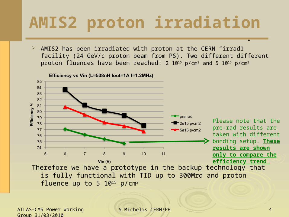
AMIS2 proton irradiation AMIS2 has been irradiated with proton at the CERN “irrad1” facility (24 GeV/c
proton beam from PS). Two different different proton fluences have been reached: 2 1015 p/cm2 and 5 1015 p/cm2
Therefore we have a prototype in the backup technology that is fully functional with TID up to 300Mrd and proton fluence up to 5 1015 p/cm2
S.Michelis CERN/PH 4ATLAS–CMS Power Working Group 31/03/2010
Please note that the pre-rad results are taken with different bonding setup. These results are shown only to compare the efficiency trend
S.Michelis CERN/PH 5ATLAS–CMS Power Working Group 31/03/2010
S2
S2
S2
S2
S2
S2
Vdd2
SUB
Enable
Enable delay
R delay
S2
D1 D1 D1 D1 D1 D1 D1 D1 IND IND IND
IND
IND
IND
IND
IND
IND
BTSTR
S2
OUT
V5V25
V18
En_B
ND
GP
En_freq
R_freq
IPT
AT
SW
1PA
D
SW
2PA
D
VFVI
VR
AM
P
VR
EF
Vss
Vdd
IND
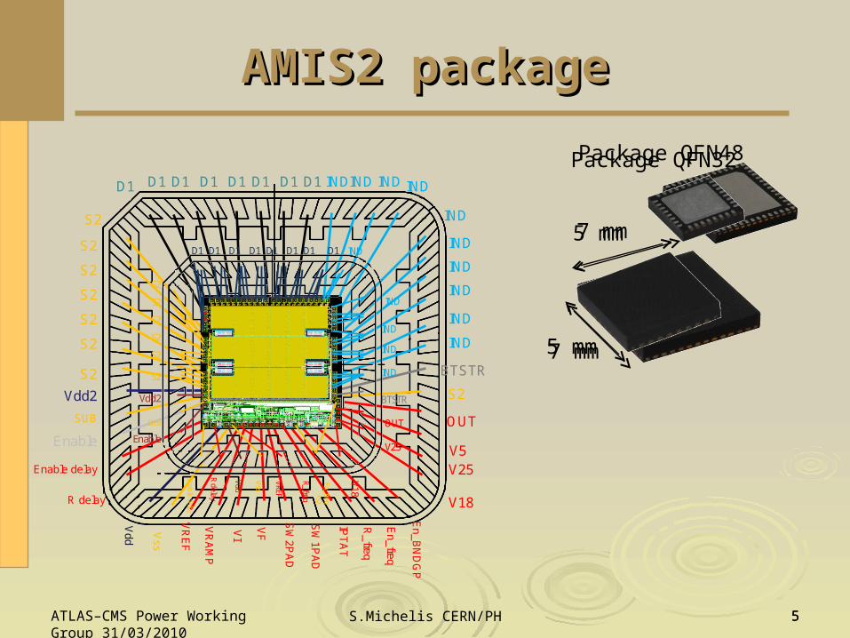
AMIS2 packageAMIS2 package
5
7 mm
7 mm
Package QFN48
5 mm
5 mm
Package QFN32
D1 D1 D1 D1 D1 D1 D1
IND
IND
IND
IND
IND
D1
S2
S2
S2
S2
S2
S2
Vdd2
SUB
Enable
Enable delay
R delay
OUT
V25
V18
En_freq+S2
R_freq
VREF
Vss
Vdd
BTSTR
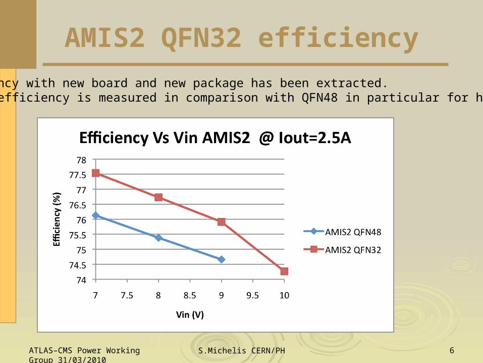
AMIS2 QFN32 efficiency
S.Michelis CERN/PH 6ATLAS–CMS Power Working Group 31/03/2010
Efficiency with new board and new package has been extracted.Higher efficiency is measured in comparison with QFN48 in particular for higher load
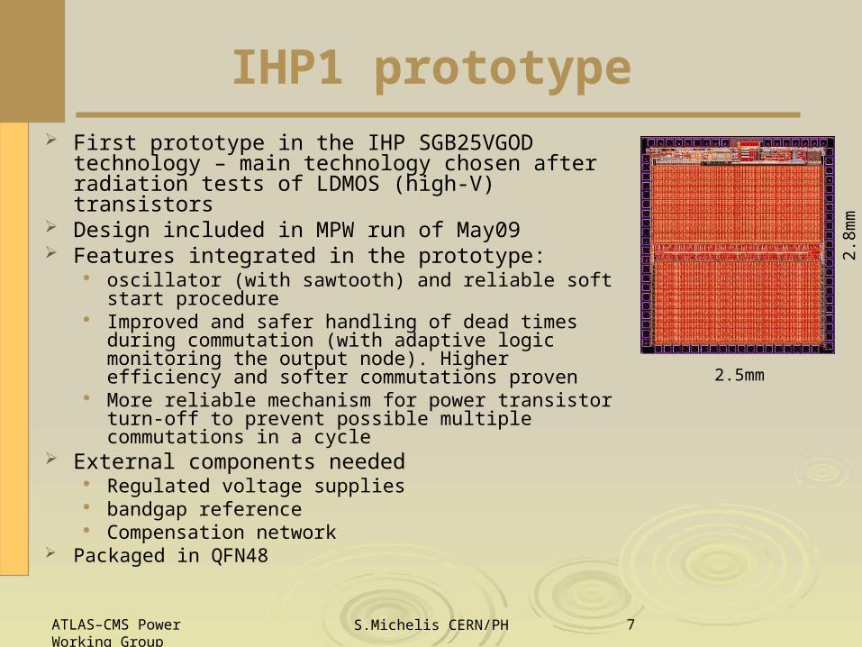
IHP1 prototype
ATLAS–CMS Power Working Group 31/03/2010
S.Michelis CERN/PH 7
First prototype in the IHP SGB25VGOD technology – main technology chosen after radiation tests of LDMOS (high-V) transistors
Design included in MPW run of May09 Features integrated in the prototype:
oscillator (with sawtooth) and reliable soft start procedure
Improved and safer handling of dead times during commutation (with adaptive logic monitoring the output node). Higher efficiency and softer commutations proven
More reliable mechanism for power transistor turn-off to prevent possible multiple commutations in a cycle
External components needed Regulated voltage supplies bandgap reference Compensation network
Packaged in QFN48
2.5mm
2.8m
m

Measurement vs Estimate
ATLAS–CMS Power Working Group 31/03/2010
S.Michelis CERN/PH 8
Vin=10V, Vout=2.5V, Iout=2A
Estimated Efficiency
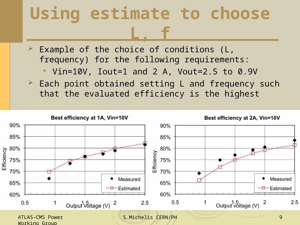
Using estimate to choose L, f
ATLAS–CMS Power Working Group 31/03/2010
S.Michelis CERN/PH 9
Example of the choice of conditions (L, frequency) for the following requirements:
Vin=10V, Iout=1 and 2 A, Vout=2.5 to 0.9V Each point obtained setting L and frequency such that the
evaluated efficiency is the highest
10
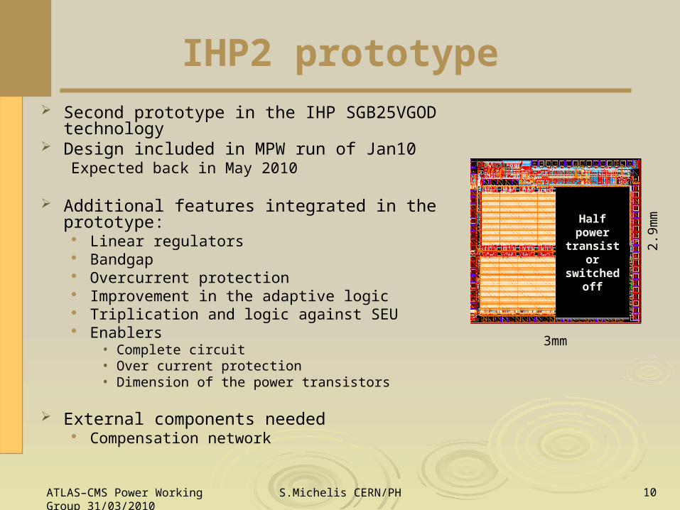
IHP2 prototype Second prototype in the IHP SGB25VGOD
technology Design included in MPW run of Jan10
Expected back in May 2010
Additional features integrated in the prototype: Linear regulators Bandgap Overcurrent protection Improvement in the adaptive logic Triplication and logic against SEU Enablers
• Complete circuit• Over current protection• Dimension of the power transistors
External components needed Compensation network
3mm
2.9m
m
ATLAS–CMS Power Working Group 31/03/2010
S.Michelis CERN/PH
Half power transistor switched
off
Half power transistor switched
off
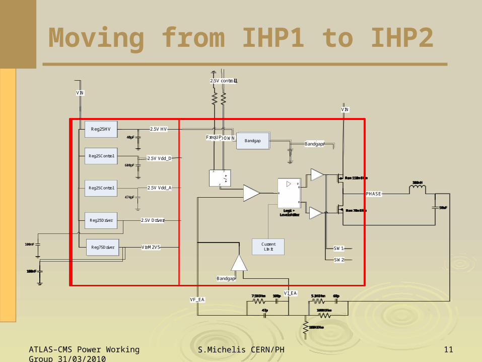
Moving from IHP1 to IHP2
68p
100KOhm
100KOhm
5.1KOhm
47p
100p7.5KOhm
300nH
50uF
Ron 110mOhm
Ron 70mOhmLogic +Level shifter
0
0
0
0
PHASE
VIN
VI_EA
VF_EA
u1
x2
x1
* / *
FreqDOWNFreqUP
SW1
SW2
2.5V
Bandgap
VIN
Bandgap
2.5V control
Reg 2.5V
Reg 1.25
VinM2V5Reg75Driver
100nF
68p
100KOhm
100KOhm
5.1KOhm
47p
100p7.5KOhm
300nH
50uF
Ron 110mOhm
Ron 70mOhmLogic +Level shifter
0
0
0
0
PHASE
VIN
VI_EA
VF_EA
u1
x2
x1
* / *
FreqDOWNFreqUP
SW1
SW2
2.5V HV
Bandgap
VIN
Bandgap
2.5V control
Reg 2.5V
Reg 1.25
VinM2V5Reg75Driver
100nF
68p
100KOhm
100KOhm
5.1KOhm
47p
100p7.5KOhm
300nH
50uF
Ron 110mOhm
Ron 70mOhmLogic +Level shifter
0
0
0
0
PHASE
VIN
VI_EA
VF_EA
u1
x2
x1
* / *
FreqDOWNFreqUP
SW1
SW2
2.5V HV
Bandgap
VIN
Bandgap
2.5V control
Reg 2.5V
Bandgap
VinM2V5Reg75Driver
100nF
68p
100KOhm
100KOhm
5.1KOhm
47p
100p7.5KOhm
300nH
50uF
Ron 110mOhm
Ron 70mOhmLogic +Level shifter
0
0
0
0
PHASE
VIN
VI_EA
VF_EA
u1
x2
x1
* / *
FreqDOWNFreqUP
SW1
SW2
2.5V HV
VIN
40pF
Bandgap
2.5V control
Reg25HV
2.5V DriverReg25Driver
100nFVinM2V5Reg75Driver
100nF
BandgapBandgap
68p
100KOhm
100KOhm
5.1KOhm
47p
100p7.5KOhm
300nH
50uF
Ron 110mOhm
Ron 70mOhmLogic +Level shifter
0
0
0
0
PHASE
VIN
VI_EA
VF_EA
u1
x2
x1
* / *
FreqDOWNFreqUP
SW1
SW2
2.5V HV
2.5V Vdd_D
VIN
40pF
600pF
Bandgap
2.5V control
Reg25HV
Reg25Control
2.5V Vdd_A
474pF
Reg25Control
2.5V DriverReg25Driver
100nFVinM2V5Reg75Driver
100nF
BandgapBandgap
68p
100KOhm
100KOhm
5.1KOhm
47p
100p7.5KOhm
300nH
50uF
Ron 110mOhm
Ron 70mOhm
PHASE
VIN
VI_EA
VF_EA
u1
x2
x1
* / *
FreqDOWNFreqUP
SW1
SW2
2.5V HV
2.5V Vdd_D
VIN
40pF
600pF
Bandgap
2.5V control
Reg25HV
Reg25Control
2.5V Vdd_A
474pF
Reg25Control
2.5V DriverReg25Driver
100nFVinM2V5Reg75Driver
100nF
BandgapBandgap
Current Limit
Logic +Level shifter
0
0
0
0
ATLAS–CMS Power Working Group 31/03/2010
11S.Michelis CERN/PH

Adaptive logic
Pmos on
Nmos on
Pmos on
Nmos on
PhaseCout
LVout
Nmos
Pmos
IL
Phase
IL
DiodeConduction
Almost zero diode conduction
Negative comp
Low side comp
High side comp
Adaptive logic allows reducing the dead time. This optimizes the switching operation and improves the efficiency
ATLAS–CMS Power Working Group 31/03/2010
12S.Michelis CERN/PH

Overcurrent protection
Pmos on
Nmos on
Pmos on
Cout
LVout
Nmos
Pmos
IL
Phase
IL
Over current sensing
2 possible cases:• Current limiter during startup• Converter restart after startup
Turn off Pmos
Over current limit
ATLAS–CMS Power Working Group 31/03/2010
13S.Michelis CERN/PH
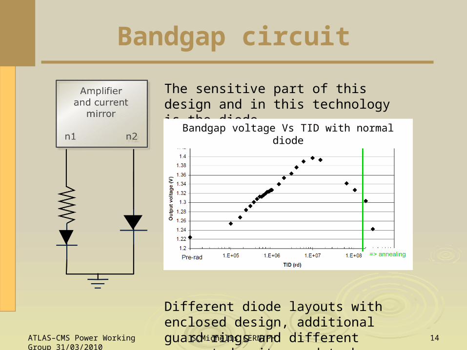
Bandgap circuit
S.Michelis CERN/PH 14ATLAS–CMS Power Working Group 31/03/2010
The sensitive part of this design and in this technology is the diode.
Different diode layouts with enclosed design, additional guard rings and different current density need to be investigated
Bandgap voltage Vs TID with normal diode
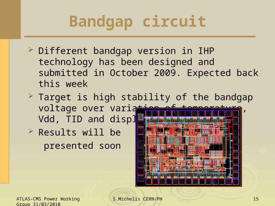
Bandgap circuit
Different bandgap version in IHP technology has been designed and submitted in October 2009. Expected back this week
Target is high stability of the bandgap voltage over variation of temperature, Vdd, TID and displacement damage.
Results will be
presented soon
ATLAS–CMS Power Working Group 31/03/2010
15S.Michelis CERN/PH
Schedule
IHP2 Mid May 2010
• 20 Chip expected back in package QFN48 May-June 2010
• Extensive functional and radiation tests July-August 2010
• Order of 100 naked chip
• Decision of necessary control pins and packaging in QFN32
IHP3 Next submission
• Investigating bump bonding Reduction of resistance of on chip metal and bondings Smaller size if direct bondend on pcb (~3x3 mm)
ATLAS–CMS Power Working Group 31/03/2010
16S.Michelis CERN/PH
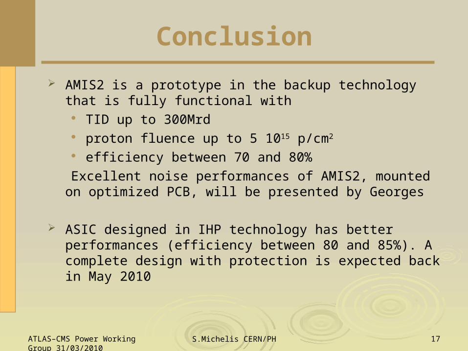
Conclusion
AMIS2 is a prototype in the backup technology that is fully functional with
TID up to 300Mrd proton fluence up to 5 1015 p/cm2
efficiency between 70 and 80%
Excellent noise performances of AMIS2, mounted on optimized PCB, will be presented by Georges
ASIC designed in IHP technology has better performances (efficiency between 80 and 85%). A complete design with protection is expected back in May 2010
S.Michelis CERN/PH 17ATLAS–CMS Power Working Group 31/03/2010