Embed Size (px)
Citation preview
DEVELOPMENT OF BULK-SCALE AND THIN FILM
MAGNETOSTRICTIVE SENSOR
Except where reference is made to the work of others, the work described in this dissertation is my own or was done in collaboration with my advisory committee. This dissertation does not include proprietary or classified information.
Cai Liang
Certificate of Approval: Bryan A. Chin Barton C. Prorok, Chair Professor Associate Professor Materials Engineering Materials Engineering Aleksandr Simonian ZhongYang (Z.-Y.) Cheng Professor Associate Professor Materials Engineering Materials Engineering Stuart Wentworth George T. Flowers Associate Professor Interim Dean Electrical & Computer Engineering Graduate School
DEVELOPMENT OF BULK-SCALE AND THIN FILM
MAGNETOSTRICTIVE SENSOR
Cai Liang
A Dissertation
Submitted to
the Graduate Faculty of
Auburn University
in Partial Fulfillment of the
Requirements for the
Degree of
Doctor of Philosophy
Auburn, Alabama December 17, 2007
iii
DEVELOPMENT OF BULK-SCALE AND THIN FILM
MAGNETOSTRICTIVE SENSOR
Cai Liang
Permission is granted to Auburn University to make copies of this dissertation at its discretion, upon request of individuals or institutions and at their expense.
The author reserves all publication rights.
Signature of Author
Date of Graduation
iv
VITA
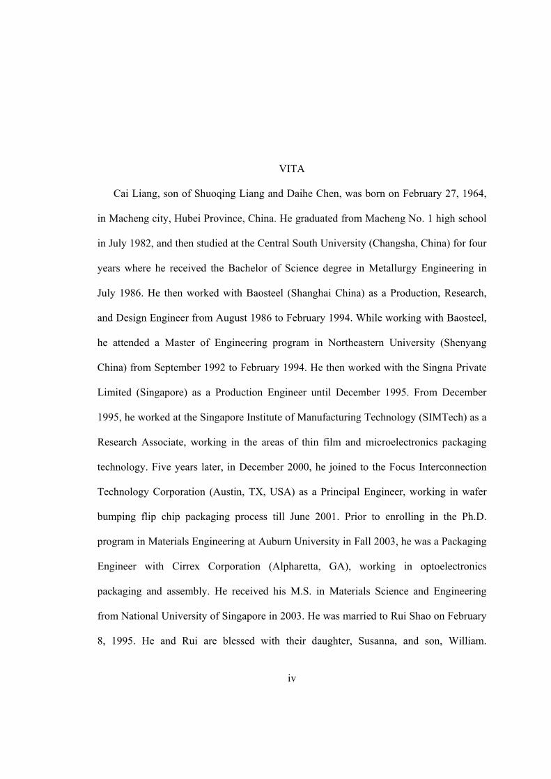
Cai Liang, son of Shuoqing Liang and Daihe Chen, was born on February 27, 1964,
in Macheng city, Hubei Province, China. He graduated from Macheng No. 1 high school
in July 1982, and then studied at the Central South University (Changsha, China) for four
years where he received the Bachelor of Science degree in Metallurgy Engineering in
July 1986. He then worked with Baosteel (Shanghai China) as a Production, Research,
and Design Engineer from August 1986 to February 1994. While working with Baosteel,
he attended a Master of Engineering program in Northeastern University (Shenyang
China) from September 1992 to February 1994. He then worked with the Singna Private
Limited (Singapore) as a Production Engineer until December 1995. From December
1995, he worked at the Singapore Institute of Manufacturing Technology (SIMTech) as a
Research Associate, working in the areas of thin film and microelectronics packaging
technology. Five years later, in December 2000, he joined to the Focus Interconnection
Technology Corporation (Austin, TX, USA) as a Principal Engineer, working in wafer
bumping flip chip packaging process till June 2001. Prior to enrolling in the Ph.D.
program in Materials Engineering at Auburn University in Fall 2003, he was a Packaging
Engineer with Cirrex Corporation (Alpharetta, GA), working in optoelectronics
packaging and assembly. He received his M.S. in Materials Science and Engineering
from National University of Singapore in 2003. He was married to Rui Shao on February
8, 1995. He and Rui are blessed with their daughter, Susanna, and son, William.
v
DISSERTATION ABSTRACT
DEVELOPMENT OF BULK-SCALE AND THIN FILM
MAGNETOSTRICTIVE SENSOR
Cai Liang
Doctor of Philosophy, December 17, 2007 (M. S. National University of Singapore, 2003) (M. E. Northeastern University, China, 1994) (B. S. Central South University, China, 1986)
258 Typed Pages
Directed by Bart Prorok
Three key areas were investigated in this research. These are: (1) finite element
modeling using modal analysis to better understand the mechanics of longitudinal
vibration system, (2) thin film material Young’s modulus measurement in a
nondestructive manner by a magnetostrictive sensor, and (3) optimization of a deposition
process for sputtering magnetostrictive thin films from Metglas 2826 MB ribbon and
machining them into useful sensor platforms.
We have verified the principle of operation for the longitudinal vibrating system
through experimentation and comparison with numerical simulations of cantilevers,
bridges, and beams. The results indicated that the governing vibration equation should
use the plane-stress or biaxial modulus. Furthermore, the Poisson’s ratio for Metglas 2826
MB was found to be 0.33. A resonating mechanical sensor was constructed from
vi
commercially available Metglas 2826 MB strip material and was used to measure
Young’s modulus of sputter deposited thin film material, e.g. Cu, Au, Al, Cr, Sn, In,
SnAu (20/80 eutectic), and SiC, with a proposed measurement methodology. The
determined Young’s modulus values were comparable to those found in the literature. In
addition, a finite element modeling analysis was employed to verify the Young’s
modulus determined by experimentation. Glass beads (size of ~425 µm) were attached to
freestanding (free-free ended) magnetostrictive sensors in order to simulate the
attachment of target species. These mass-loading results indicated that the frequency
shifts are sensitive to the location of the mass on the sensor’s surface. Finite element
analysis was conducted and ascertained that when a particle comparable in size to E. Coli
O157 cell (mass in pico-gram range) attaches to sensor of 250 x 50 x 1.5 microns in size,
a significant resonant frequency shift results, indicating that the sensor has the potential
to detect the attachment of a single bacterium. These simulations also confirm that the
resonant frequency shift is dependent on the location of the mass attachment along the
longitudinal axis of the sensor.
Finally, a process for depositing magnetostrictive thin film material from directly
sputtering of Metglas 2826 MB ribbon was developed. Microscale sensors were
fabricated with this film material. Dynamic testing of these microscale sensors was
carried out on freestanding particles of the size 500 x 100 x 3 microns. The resonant
frequency of these microfabricated particles was found to increase significantly in both
magnitude and amplitude after the particle was annealed. A model was employed to
explain why the magnetoelastic sensor behavior changed after annealing.
vii
ACKNOWLEDGEMENTS
I have been blessed so much during my study while living in Auburn. Many faculty
members, friends, and family members deserve my greatest appreciation. The foremost
thanks go to my advisor, Dr. Bart Prorok for his constant support and guidance; without
his encouragement, this research will not be interesting or meaningful. I am also grateful
to Dr. Bryan Chin, Dr. Aleksandr Simonian, Dr. ZhongYang Cheng, Dr. Stuart
Wentworth, and Dr. Jeffrey Suhling for their timely review of my work, fruitful
discussions and precious suggestions. I am grateful for Drs. Dongye Zhao and Rob
Martin’s help in preparation of this dissertation. I appreciate Dr. Chin-Che Tin, Dr. John
R. Williams, Dr. Minseo Park, Dr. Curtis Shannon and Dr. Rainer Schad from the
University of Alabama at Tuscaloosa for helping with various experiments. Thanks also
due to Mr. Charles Ellis, Ms. Shirley Lyles, Mr. L. C. Mathison, and Mr. Roy Howard. I
must also express my gratitude to many friends and their families, Drs. Morris Bian,
Dongye Zhao, Wenhua Zhu, Wei Wang, Daowei Zhang, and Dr. Cankui Zhang’s
encouragements and help in one way or another. Group members, fellow graduate
students, and many friends deserve my thanks as well. I am most indebted to my wife,
Rui Shao, my daughter, Susanna, and son, William, for their support, substantial patience
and genuine love. Susanna forgave me for not fixing her bicycle in time and not attending
many of her school and other programs. William let me off for not helping him much in
the sale of popcorn as a Cub Scout. I acknowledge financial support from AUDFS Center.

viii
DEDICATED
To the memory of my parents and my eldest sister,
whose love and encouragements led me on the road of scientific research
and
To my wife, daughter, son, and other family members,
for their love, unconditional support, and encouragements.
ix
Style Manual or J. used: IEEE Transaction on Components and Packaging Technology
Computer software used: Microsoft Office, Matlab, SAS, Sigmaplot 8.0, and CAD
x
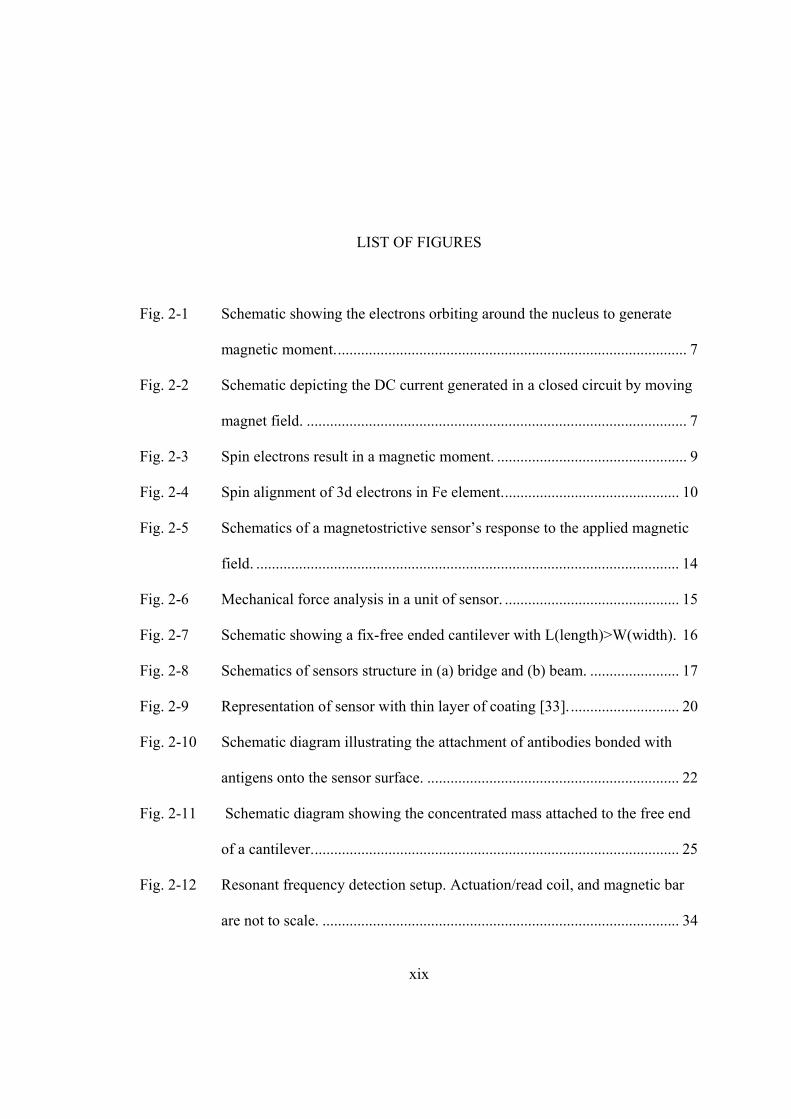
TABLE OF CONTENTS LIST OF TABLES …………………………………………………………...………. xxii
LIST OF FIGURES…...……………………………………………………………….xxiv
1. INTRODUCTION ..................................................................................................... 1
1.1. Motivation for Research ................................................................................... 1
1.1.1. Development of Mechanical Sensor for Thin Film Property
Measurement........................................................................................... 1
1.1.2. Development of Biosensors ..................................................................... 2
1.2. Objectives of This Research ............................................................................. 2
1.3. An Overview of the Contents ........................................................................... 4
2. MAGNETOSTRICTION AND MAGNETOSTRICTIVE SENSORS..................... 6
2.1. Fundamentals of Magnetostrictive Materials.................................................... 6
2.1.1. Magnetic Properties of Materials............................................................. 6
2.1.2. Magnetostrictive Behavior and Magnetoelastic Interactions of Magnetic
Materials................................................................................................ 11
2.2. Magnetostrictive Sensor Operation in the Longitudinal Vibration Mode ...... 13
2.2.1. Fix-Free Ended Cantilever Sensor ......................................................... 16
2.2.2. Fix-Fix and Free-Free Ended Sensors.................................................... 17
2.3. Application of Magnetostrictive Sensors.........................................................18
xi
2.3.1. Mechanical Sensor for Measuring Young’s Modulus of Thin Film
Material ................................................................................................. 19
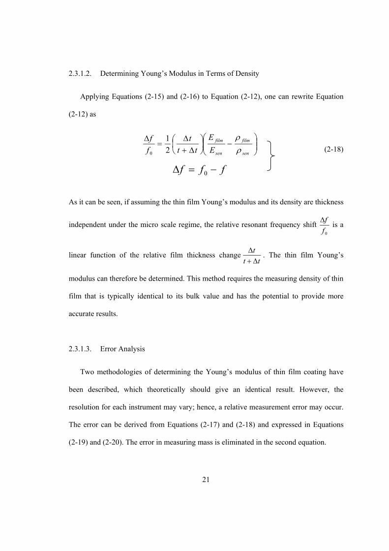
2.3.1.1. Determining Young’s Modulus in Terms of Mass ................ 20
2.3.1.2. Determining Young’s Modulus in Terms of Density ............ 21
2.3.1.3. Error Analysis........................................................................ 21
2.3.2. Mass Sensor for Analyzing Chemicals or Biochemical Agents ............ 22
2.3.2.1. Mass Sensor with Uniformly Distributed Mass Attachment. 23
2.3.2.2. Mass Sensor with a Concentrated Mass Attachment............. 24
2.4. Methodology of Detecting the Resonant Frequency of a Magnetostrictive
Sensor.............................................................................................................. 33
3. FUNDAMENTALS AND ADVANTAGES OF A SENSOR VIBRATING IN THE
LONGITUDINAL MODE....................................................................................... 39
3.1. Comparison of the Fundamentals of Vibrating a Cantilever, Bridge, or Beam
System............................................................................................................. 39
3.1.1. The Transverse Mode ............................................................................ 39
3.1.1.1. Actuation Techniques ............................................................ 39
3.1.1.2. Sensing Techniques ............................................................... 40
3.1.2. The Longitudinal Mode ......................................................................... 41
3.2. Advantages of Vibrating a Cantilever, Bridge, and Beam in the Longitudinal
Mode Over the Transverse Mode ................................................................... 42
3.2.1. Comparison of the Resonant Frequency Magnitude for the Two
Vibration Modes ................................................................................... 42
3.2.2. Comparison of Sensitivity for Two Vibration Modes ........................... 45
xii
3.3. Minimum Sensor Geometry Required for Detection of a Single
Biomolecule….. .............................................................................................. 48
3.4. Summary ......................................................................................................... 50
4. CORRECTION TO THIN, SLENDER BEAM VIBRATING IN THE
LONGITUDINAL MODE PRINCIPLE AND VALIDATION OF PROOF-OF-
CONCEPT EQUATIONS ....................................................................................... 52
4.1. Introduction..................................................................................................... 52
4.2. Determination of the Correct Analytical Solution for Thin Slender Beams... 57
4.3. Experimental Test and Numerical Analysis to Verify the Longitudinal Mode
Proof-of-Principle ........................................................................................... 64
4.3.1. Experimental verification of the Proof-of-Principle Equations ............. 64
4.3.2. Numerical verification of the Proof-of-Principle Equations.................. 67
4.4. Discrepancy Analysis of the Resonant Frequency Obtained by Experimental
Measurement, Finite Element Simulation, and Numerical Calculation ......... 71
4.5. Summary ......................................................................................................... 74
5. BULK-SCALE MAGNETOSTRICTIVE SENSORS............................................. 75
5.1. Thin Film Elastic Modulus Measurement....................................................... 75
5.1.1. Experimental Details.............................................................................. 82
5.1.2. Results and Discussion .......................................................................... 83
5.1.2.1. Surface Morphology of Deposited Thin Film Materials of Au,
Cu, Al, Cr, In, Sn, AuSn (80/20), and SiC ............................ 83
5.1.2.2. Crystal Structure of Sputtering Deposited Thin Film............ 89
5.1.2.3. Sensor Response to Various Thin Film Coatings.................. 92
xiii
5.1.2.4. Sensor Response to the Applied Magnetic Field and Figure-of-
merit Q Values....................................................................... 97
5.1.2.5. Determination of Young’s Modulus for Thin Film
Materials…… ...................................................................... 104
5.1.2.6. Comparison of Au Film Young’s Modulus Obtained by
Different Methods and Measuring Techniques ................... 107
5.1.2.7. Finite Element Analysis to Verify Thin Film Young’s
Modulus Measurement ........................................................ 109
5.1.2.8. Comparison of Error Resulting From Different Methodologies
and for A Variety of Film Materials .................................... 113
5.2. Concentrated Mass Detection ....................................................................... 115
5.2.1. Experimental Details............................................................................ 119
5.2.2. Results and Discussion ........................................................................ 120
5.2.3. Finite Element Simulation Analysis to Verify the Mass Detection for
Mass Concentrations ........................................................................... 126
5.2.3.1. Results of Resonant Frequency Change Due to a Single Cell
Attachment........................................................................... 129
5.2.3.2. Influence of Different Orientations of the Asymmetrical
Cells…. ................................................................................ 131
5.2.3.3. Influence of Off-Centerline Attachment.............................. 132
5.2.3.4. Influence of Randomly Attached Multiple Masses ............. 135
5.3. Summary ....................................................................................................... 137
xiv
6. DEPOSITION OF MAGNETOSTRICTIVE THIN FILM MATERIAL AND
CHARACTERIZATION OF MICROFABRICATED MICROSCALE
SENSORS….......................................................................................................... 140
6.1. Magnetostrictive/Magnetoelastic Thin Films ............................................... 140
6.2. Introduction to Physical Vapor Deposition and Sputter Deposition
Technology… ............................................................................................... 143
6.3. Experimental Details..................................................................................... 151
6.3.1. Fabrication of Sputtering Target.......................................................... 152
6.3.2. Design of the Sputter Deposition Process............................................ 153
6.3.3. Characterization of Magnetostrictive Thin Film.................................. 155
6.3.4. Magnetostrictive Thin Film Annealing................................................ 155
6.3.5. Microfabrication of Magnetostrictive Sensors..................................... 156
6.4. Results and Discussion ................................................................................. 159
6.4.1. Initial Approach of Deposition of Magnetostrictive Thin Film by Phase I
............................................................................................................. 159
6.4.1.1. Deposition Rate ................................................................... 159
6.4.1.2. Surface Morphology and Crystal Structure of Deposited
Magnetostrictive Thin Films ............................................... 160
6.4.1.3. Magnetic Properties of Deposited Magnetostrictive Thin
Film…….............................................................................. 163
6.4.1.4. Thin Film Composition Analysis ........................................ 168
6.4.2. DOE (Design of Experiment) Approach of Sputter Deposition by Phase
II .......................................................................................................... 173
xv
6.4.2.1. Deposition Rate and Surface Morphology Influenced by
Various Factors.................................................................... 173
6.4.2.2. Magnetic Properties Impacted by Various Factors.............. 176
6.5. Microfabrication and Functionality Test of Magnetostrictive Cantilever and
Bridge Type Sensor....................................................................................... 180
6.5.1. Microfabrication of Cantilever and Bridge Type Sensors ................... 180
6.5.2. Functionality Tests of Cantilever and Bridge Sensors......................... 183
6.6. Microfabrication and Resonant Frequency Test of Magnetostrictive
Freestanding Beam (Particle)........................................................................ 185
6.6.1. Free-free ended Beam (Particle) Fabrication....................................... 185
6.6.2. Results of Resonance Frequency Tests................................................ 188
6.6.3. Annealing Effect .................................................................................. 188
6.6.3.1. Effect of annealing on Magnetic Properties ........................ 189
6.6.3.2. Effect of annealing on the Resonance Frequency and Q-Factor
of Sensor .............................................................................. 190
6.6.3.3. Mechanisms on the Annealing Effects ................................ 193
6.7. Summary ....................................................................................................... 198
7. CONCLUSION AND FUTURE WORK .............................................................. 199
7.1. Conclusions................................................................................................... 199
7.2. Future work................................................................................................... 201
REFERENCES....………………………………………………………………………202
xvi
LIST OF TABLES
Table 2-1 Calculated the roots (kL values) for Equation (2-37) at different η values..29
Table 2-2 Calculated relative resonant frequency changes for a concentrated mass
attached to the free end and an evenly distributed mass with the same
amount as a concentrated one at a different ratio of this attached mass to the
sensor mass (η)............................................................................................. 30
Table 2-3 Calculated kL values from Equation (2-48) and relative resonant frequency
shift from Equation (2-49) at a different ratio (η) of attached mass to the
free-free ended beam mass........................................................................... 32
Table 3-1 Essential geometry of a cantilever and bridge sensor designed for detecting a
single biomolecule. ...................................................................................... 50
Table 4-1 Comparison of resonant frequencies calculated by using E and plane-strain
modulus E/(1-ν2) with experimental test for freestanding beam cantilever
and bridge at different lengths. .................................................................... 55
Table 4-2 Specimen’s size and aspect ratio.................................................................. 58
Table 4-3 Simulated results of resonant frequencies for different Poisson’s ratio inputs,
where n was calculated based on Equation (4-3)......................................... 63
Table 4-4 Comparison of the measured and calculated resonant frequencies (kHz) for
three structures. ............................................................................................ 63
xvii
Table 4-5 Resonant frequency obtained by simulation for a cantilever (80 µm x 20 µm
x 1.0 µm) made of Metglas. ......................................................................... 68
Table 4-6 Resonant frequency obtained by simulation for a bridge (14.4 mm x 3.0 mm
x 28 µm) made of Metglas. .......................................................................... 70
Table 4-7 Resonant frequency obtained by simulation for a beam (8 mm x 1.6 mm x
28 µm) made of Au...................................................................................... 70
Table 4-8 Sensor size, materials, and type used for simulation and experiment. ........ 72
Table 4-9 Analysis of the differences of resonant frequency obtained by calculation,
simulation, and experimentation.................................................................. 72
Table 5-1 Highest temperature of near substrate surface reached during deposition .. 89
Table 5-2 Comparison of Young’s modulus for thin film materials tested in this work
and their bulk scale counterpart [118-121]. ............................................... 105
Table 5-3 Summary of process, test method, and value for various thin film materials,
methods in italics are non-destructive methods. ........................................ 106
Table 5-4 Materials properties used for finite element analysis. ............................... 111
Table 5-5 Minimal detectable concentration for SAW and FPW [144]..................... 117
Table 5-6 Comparison of mass sensors...................................................................... 118
Table 5-7 Test results of sensor (5 mm x 1 mm x 28 µm) attached with glass bead at
different locations. ..................................................................................... 122
Table 5-8 Summary of simulation results of frequency changes and sensitivities for the
three types of sensors in response to E Coli O157 cells bonded onto a (250
µm x 5 µm x 5 µm) sensor’s surface ......................................................... 137
Table 6-1 Magnetic materials and related criteria for their applications [188].......... 142

xviii
Table 6-2 Comparison of evaporation and sputtering techniques [206]. ................... 144
Table 6-3 DOE parameters and variables................................................................... 154
Table 6-4 L4(23) matrix for DOE ............................................................................... 155
Table 6-5 Compositions of Metglas 2826 MB and magnetostrictive films. .............. 169
xix
LIST OF FIGURES
Fig. 2-1 Schematic showing the electrons orbiting around the nucleus to generate
magnetic moment........................................................................................... 7
Fig. 2-2 Schematic depicting the DC current generated in a closed circuit by moving
magnet field. .................................................................................................. 7
Fig. 2-3 Spin electrons result in a magnetic moment. ................................................. 9
Fig. 2-4 Spin alignment of 3d electrons in Fe element.............................................. 10
Fig. 2-5 Schematics of a magnetostrictive sensor’s response to the applied magnetic
field. ............................................................................................................. 14
Fig. 2-6 Mechanical force analysis in a unit of sensor. ............................................. 15
Fig. 2-7 Schematic showing a fix-free ended cantilever with L(length)>W(width). 16
Fig. 2-8 Schematics of sensors structure in (a) bridge and (b) beam. ....................... 17
Fig. 2-9 Representation of sensor with thin layer of coating [33]............................. 20
Fig. 2-10 Schematic diagram illustrating the attachment of antibodies bonded with
antigens onto the sensor surface. ................................................................. 22
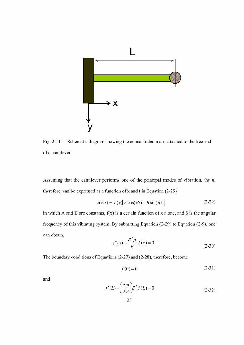
Fig. 2-11 Schematic diagram showing the concentrated mass attached to the free end
of a cantilever............................................................................................... 25
Fig. 2-12 Resonant frequency detection setup. Actuation/read coil, and magnetic bar
are not to scale. ............................................................................................ 34
xx
Fig. 2-13 S-parameters flow diagram. ......................................................................... 35
Fig. 2-14 S11 change with the swept frequency. .......................................................... 36
Fig. 2-15 Impedance change as a function of the swept frequency............................. 37
Fig. 3-1 Comparison of cantilever resonant frequency operated in different modes. 44
Fig. 3-2 Comparison of bridge resonant frequency operated in different modes...... 44
Fig. 3-3 The sensitivity ratio ⎟⎟⎠
⎞⎜⎜⎝
⎛
L
T
SS of a cantilever sensor as a function of sensor
geometry. ..................................................................................................... 47
Fig. 3-4 The sensitivity ratio ⎟⎟⎠
⎞⎜⎜⎝
⎛
L
T
SS of bridge sensor as a function of sensor
geometry…… .............................................................................................. 47
Fig. 3-5 Change in sensitivity of a cantilever in the transverse mode by size........... 49
Fig. 3-6 Change in sensitivity of a cantilever in the longitudinal mode by size. ...... 49
Fig. 4-1 Schematic diagram of setup for resonant frequency testing in (a)cantilever
and (b) bridge............................................................................................... 58
Fig. 4-2 Measured resonant frequency of sensor vs. sensor’s length at aspect ratio =
4…................................................................................................................ 59
Fig. 4-3 Measured resonant frequency of sensor vs. sensor’s length at aspect ratio =
10….............................................................................................................. 60
Fig. 4-4 Operator number (n) as a function of Poisson’s ratio (ν) obtained by
experiments and simulations........................................................................ 60
Fig. 4-5 Result of an 8 mm x 1.6 mm x 28 µm sensor meshed with 160 µm x 160 µm
x 5.6 µm element size. ................................................................................. 62
Fig. 4-6 Resonant frequency of the first two modes for a 14.4 mm cantilever. ........ 65
xxi
Fig. 4-7 Resonant frequency of the first two modes for a 14.4 mm bridge............... 65
Fig. 4-8 Resonant frequency of the first two modes for cantilever array.................. 66
Fig. 4-9 Typical mode shapes at different orders of mode for a cantilever in
longitudinal vibration................................................................................... 69
Fig. 4-10 Simulation results for freestanding Metglas beam with the size of 8 mm x
1.6 mm x 28 µm. Poisson’s ratio of 0.35 was employed............................. 73
Fig. 5-1 Schematic diagram illustrating bulge test method [67]. .............................. 77
Fig. 5-2 Schematic of the microbend test [68]. ......................................................... 77
Fig. 5-3 Schematic of microbeam deflection test method in (a) deflection by
electrostatic force [71], and (b) deflection by nanoindentation [72]. .......... 78
Fig. 5-4 Schematic depicting the method by dynamic vibrating cantilever in resonant
frequency. (a) A laser detector is generally used to detect the frequency [77],
and (b) a microfabricated SiO2 cantilever array is used for the resonant
frequency test [82]. ...................................................................................... 78
Fig. 5-5 Schematic depicting the nanoindentation test method [101]. ...................... 80
Fig. 5-6 SEM images of film surface morphology. The material of the film and its
thickness is indicated on each image. .......................................................... 86
Fig. 5-7 SEM images of Au film with thicknesses of 0.1 µm, 0.25 µm, 0.50 µm,
0.855 µm, 1.10 µm, 1.50 µm. ...................................................................... 88
Fig. 5-8 XRD patterns for thin films deposition on Metglas sensors. ....................... 90
Fig. 5-9 XRD pattern for Au and solder thin film materials. .................................... 90
Fig. 5-10 Au rich portion of Au-Sn equilibrium phase diagram [114]........................ 91
Fig. 5-11 EDX analysis of AuSn solders composition................................................ 91
xxii
Fig. 5-12 Resonant frequency changes before and after thin film coating. The left
panel shows the decrease in frequency after Au coating deposition, and the
right panel shows increase in frequency after Cr coating deposition [33]... 93
Fig. 5-13 Relative resonant frequency change as a function of relative thin film
thickness ratio. ............................................................................................. 94
Fig. 5-14 Relative frequency changes vs. Au film for various sensor thicknesses based
on Equation (2-18). ...................................................................................... 96
Fig. 5-15 Relative frequency changes vs. Cr film for various sensor thicknesses based
on Equation (2-18). ...................................................................................... 96
Fig. 5-16 Frequency response of sensor (8 mm x 1.6 mm x 28 µm) coated with 0.55
µm indium film to the applied DC magnetic field....................................... 99
Fig. 5-17 Frequency and its amplitude change with normalized external field strength
(DC bias)...................................................................................................... 99
Fig. 5-18 Q value for sensors coated with and without 0.55 µm indium thin film. .. 102
Fig. 5-19 Q values for a sensor without coating or with Cu coating of various
thickness..................................................................................................... 102
Fig. 5-20 Q value for sensors deposited with Cu and Cr film in different thickness.103
Fig. 5-21 Plot of Young’s modulus determined in this work with other literature
data……..................................................................................................... 105
Fig. 5-22 Young’s modulus of Au film obtained by measuring the masses of the
sensors and films........................................................................................ 108
xxiii
Fig. 5-23 Relative frequency change vs. relative Au thin film thickness change and its
corresponding Young’s modulus obtained by measuring the masses of the
sensor and film [130]. ................................................................................ 108
Fig. 5-24 Young’s modulus of Au film measured at different thickness by
magnetostric-tive sensor and MDE [130]. ................................................. 109
Fig. 5-25 Typical mesh model of a sensor coated with Au film. .............................. 111
Fig. 5-26 Experimental and simulated results of the relative frequency change with the
relative thickness........................................................................................ 112
Fig. 5-27 Relative error of Young’s modulus analysis for the methods applied in
determining Au thin film material. ............................................................ 114
Fig. 5-28 Relative error of Young’s modulus for various thin film materials........... 114
Fig. 5-29 SEM images showing glass beads attached to the sensor in various locations.
The numbers correspond to the test numbers listed in Table 5-7….. ........ 121
Fig. 5-30 Resonant frequency spectrum of a sensor (5 mm x 1 mm x 28 µm) with and
without glass bead attached to its center.................................................... 122
Fig. 5-31 Resonant frequency change due to glass bead attached to one of the free
ends of a sensor (5 mm x 1 mm x 28 µm). ................................................ 123
Fig. 5-32 Resonant frequency change as a function of the location of a glass bead
attached to the surface of a sensor of 5.0 mm x 1.0 mm x 28 µm. ............ 125
Fig. 5-33 Relative resonant frequency change as a function of the location of a glass
bead attached to the surface of a sensor of 5.0 mm x 1.0 mm x 28 µm..... 125
Fig. 5-34 Schematic diagram of the mass loaded on a sensor (250 µm x 50 µm)
surface. ....................................................................................................... 127
xxiv
Fig. 5-35 Model meshing results for (a) a single cell and (b) multiple cells on a
sensor…… ................................................................................................. 128
Fig. 5-36 Frequency shift of various structured sensors (sensitivity in this case) as a
function of cell location along the central line........................................... 130
Fig. 5-37 An E. Coli cell orientated along the longitudinal axis at (x = 0, y = 225). 131
Fig. 5-38 An E. Coli orientated perpendicular to the longitudinal axis at (x = 0, y =
225). ........................................................................................................... 132
Fig. 5-39 Simulation results of an E. Coli cell orientated parallel to the longitudinal
axis at (x = 20, y = 225). ............................................................................ 133
Fig. 5-40 Sensitivity of cantilever to biomolecule distribution on the surface.......... 134
Fig. 5-41 Sensitivity of beam to biomolecule distribution on the surface................. 134
Fig. 5-42 Sensitivity of bridge to biomolecule distribution on the surface. .............. 135
Fig. 6-1 Schematic depiction of sputter deposition process. ................................... 146
Fig. 6-2 Schematics of (a) a target assembly and (b) electrical and magnetic fields’
orientation related to a target. .................................................................... 147
Fig. 6-3 Paschen curve for breakdown potential between parallel electrodes
[210]……................................................................................................... 150
Fig. 6-4 Photo showing the sputter system with plasma on. ................................... 150
Fig. 6-5 Photo pictures of Metglas targets showing surface erosion after sputtering at
different times. ........................................................................................... 153
Fig. 6-6 Micromachining process for cantilever sensor (not to scale). ................... 157
Fig. 6-7 Basic procedure for lift-off sensors............................................................ 158
Fig. 6-8 Deposition rate as a function of process pressure change.......................... 160
xxv
Fig. 6-9 SEM surface images for sputter deposited magnetostrictive thin film under
different process pressure, (a) pressure = 5 mT, (b) pressure = 10 mT, and (c)
pressure = 20 mT. Note the difference in magnification between them.... 161
Fig. 6-10 XRD spectra for sputter deposited magnetostrictive films under different
pressures..................................................................................................... 163
Fig. 6-11 Hysteresis loop for magnetostrictive films deposited under different
pressures..................................................................................................... 164
Fig. 6-12 General hysteresis loop of a hard magnetic material. ................................ 165
Fig. 6-13 Magnetic properties of magnetostrictive thin film as affected by deposition
pressure. ..................................................................................................... 165
Fig. 6-14 Hysteresis loop for the Metglas 2826 MB ribbon...................................... 166
Fig. 6-15 B-H curves of pure Ni under different stress orientation to the external
magnetic field, (a) tensile stress parallel to the applied field and (b) tensile
stress perpendicular to the applied field [188]. .......................................... 168
Fig. 6-16 AES spectra of Metglas and thin film deposited at various pressures. (a)
Metglas, (b) 5 millitorr, (c) 10 millitorr, and (d) 20 millitorr. ................... 171
Fig. 6-17 XPS spectra of Metglas and thin film deposited at various pressures. (a)
Metglas, (b) 5 millitorr, (c) 10 millitorr, and (d) 20 millitorr .................... 172
Fig. 6-18 Thin film deposition rate change with various deposition parameters. ..... 174
Fig. 6-19 Surface morphology of deposited films. (#1, #2, #3, and #4 correspond to
the experiments of 1 to 4 in Table 6-4)...................................................... 175
Fig. 6-20 Hysteresis loop for magnetostrictive film deposited under various conditions
but with the same applied field orientation................................................ 177
xxvi
Fig. 6-21 Hysteresis loop for films deposited under conditions preset in the DOE. #1,
#2, #3, and #4 refer to experiment run number set by the DOE in Table 6-
4….............................................................................................................. 178
Fig. 6-22 Coercity change with each individual factor and variable......................... 179
Fig. 6-23 Microscopic images of Al open windows for the etch SiN. (a) Cantilever (b)
Bridge......................................................................................................... 181
Fig. 6-24 Microscopic images of cantilevers and bridges after Si wet etching......... 181
Fig. 6-25 SEM images for cantilevers and bridge. (a) and (b) are cantilevers with
different aspect ratio, (c) is a fix-fix ended bridge..................................... 182
Fig. 6-26 SEM images for cantilevers and bridges coated with ~ 4 µm FeB thin
films….. ..................................................................................................... 184
Fig. 6-27 SEM images of microfabricated photo resist templates for the fabrication of
freestanding sensors. .................................................................................. 186
Fig. 6-28 SEM image of a freestanding beam (particle) on PR template.................. 186
Fig. 6-29 SEM images of some uncollected, lift-off freestanding beams (particles).
The bent particles appeared to be stressed................................................. 187
Fig. 6-30 Resonant frequency spectrum for a 500 µm x 100 µm beam (particle). ... 187
Fig. 6-31 Temperature changes with time during annealing/cooling process........... 188
Fig. 6-32 Hysteresis loops of sputtering deposited films before and after annealing at
215oC for two hours in a vacuum chamber................................................ 189
Fig. 6-33 Resonant frequency shift of a particle after annealing............................... 190
Fig. 6-34 Peak profiles of resonant frequency spectra for different sensors with
various Q values......................................................................................... 192
xxvii
Fig. 6-35 SEM images of an annealed sensor. A slight curvature in the width direction
can be seen, but not in the longitudinal direction. (a) Bottom surface is up.
(b) Bottom surface is down........................................................................ 194
Fig. 6-36 Modeling of a sensor bent in longitudinal direction. ................................. 196
Fig. 6-37 Modeling of a perfect sensor without bending. ......................................... 197
Fig. 6-38 Modeling of an annealed sensor that is only bent in the lateral axis, but not
in the longitudinal direction. ...................................................................... 197
1
1. INTRODUCTION
1.1. Motivation for Research
1.1.1. Development of Mechanical Sensor for Thin Film Property Measurement
For decades, researchers and engineers have extensively applied thin film materials in
microelectronics for very- to ultra-large-scale-integrated (VLSI/ULSI) circuit and
microelectromechanical systems (MEMS) or microsystems technology (MST). The
mechanical properties such as Young’s modulus of thin film materials are commonly
unknown and assumed to be similar to their bulk values. However, the mechanical
properties of thin films may differ from their bulk counterparts due to differences in
operating deformation mechanisms, material texture, and other microstructural issues.
Although many techniques have been explored to assess this issue, most are destructive,
time consuming, and expensive to perform. Most require the tests to be conducted on the
thin film materials constructed by microfabrication processes that increase the
measurement cost. Furthermore, the additional microfabrication process may influence
the thin film properties [1]. A standard method for measuring thin film mechanical
properties that is nondestructive, quick, easy, and cost effective to perform does not yet
exist.

2
1.1.2. Development of Biosensors
Since September 11, 2001, security monitoring has become a growing concern in
virtually every country, which in turn has driven the research and development of
advanced devices and technologies to protect, detect, and trace biological species by
unintentional biological attack. The area of food safety is included in these new security
concerns, and a way to monitor food production from the farm through production
process and the supply chain to customers is in growing demand. In the United States, it
has been estimated that nearly 76 million people suffer from food-borne illnesses each
year, accounting for 325,000 hospitalizations and more than 5,000 deaths [2, 3]. Recently
it was reported that lettuce and spinach contaminated with E. Coli O157:H7 caused
sickness in twenty-eight people and one death [4, 5], which further indicates that food
safety is extremely important to human lives. The development of an advanced device
that can simply and quickly detect any harmful bio-agent threats in food products is
becoming an important challenge. The development of mesoscale and microscale sensor
platforms based on MEMS/MTS technology has shown great promise and represents a
paradigm shift in homeland security and anti-terrorism efforts. In addition, MEMS
sensors offer the advantages of vastly reduced sample consumption and little to no by-
products, as are typically produced in chemical and biochemical analyses.
1.2. Objectives of This Research
The objectives of this work had two main themes (1) to study and improve
magnetostrictive strip fashioned from Metglas 2826 MB ribbon as sensors platforms and
3
(2) to develop a deposition process for constructing magnetostrictive thin film from
Metglas 2826 MB for MEMS and sensors applications. In accomplishing these goals this
work was divided into three areas where experimental and numerical interrogation were
employed in the design and characterization of these sensors. These are:
1). Finite element modeling using modal analysis to better understand the mechanics
of actuation of magnetostrictive forms.
The proof-of-principle of a sensor designed in resonating cantilever, bridge, and
freestanding forms in their longitudinal mode will be studied by experimentation and
simulation. The analytical solution for predicting the resonant frequency of a
magnetostrictive sensor will be verified, and if necessary, be modified to express the
correct state of strain on the magnetostrictive form. The approach will involve combining
experimentally determined behavior that will be verified by FEA study. This will include
characterizing the resonant frequency shift of a sensor due to deposition of a thin film
material, a single and multiple bimolecular cells attached to its surface, and their position,
or orientation, on the sensor.
2). Developing a highly accurate magnetostrictive sensor for measuring the elastic
modulus of a thin film and detecting a concentrated mass on the sensor’s surface.
Here, a bulk scale magnetostrictive sensor will be constructed from Metglas 2826
MB ribbon and used to measure the elastic properties of sputter deposited Cu, Au, Cr, Sn,
Sn-Au, etc. thin films. An improved methodology of determining Young’s modulus of a
thin film material was introduced, which is more similar but also more accurate than
existing techniques. The results will be compared with many popular but complicated
techniques, such as the membrane deflection experiments, and will be verified by finite
4
element modeling analysis. A glass bead as a concentrated mass will be attached to a
bulk-scale sensor to determine the sensor’s response to this unevenly distributed mass.
Simulation will be employed to study the effect of a mass compatible to an E. Coli cell on
the sensor.
3). Developing a deposition process for sputtering thin films from Metglas 2826 MB
ribbon and micromachining them into useful sensor platforms. A feasibility study of
directly sputtering magnetostrictive target material (Metglas 2826 MB) to form a
magnetostrictive thin film will be the primary focus of this area. The sputter target will be
fabricated from Metglas 2826 MB ribbon. A systemic study will be applied to the process
of deposition towards obtaining optimized thin film properties. Finally, microscale
sensors will be fabricated from the sputtering deposited magnetostrictive thin film, and
will be characterized for their potential application in detection of chemical and
biochemical agents.
1.3. An Overview of the Contents
This dissertation consists of seven sections, including the introduction. The second
section gives a general overview of the principles of magnetostrictive sensors and the
potential applications of such sensors in measuring Young’s modulus of thin film and
biochemical agents. Details of the magnetostrictive sensors’ resonant frequency
measurements are discussed in this section as well. The third section is a more detailed
discussion the fundamentals and advantages of a sensor vibrating in the longitudinal
mode over the transverse mode. The strategy of sensor design for detecting a single
biomolecule is discussed. Section four reports the finite element simulation results of
5
magnetostrictive sensors for the two applications mentioned above. In conjunction with
experimental data, the Poisson’s ratio of Metglas 2826 MB is determined and its
influence on the theoretic calculation of resonant frequency is discussed. The proof-of-
principle of a cantilever and bridge sensor operated in longitudinal mode is verified by
both experimentation and simulation.
Section five details the methodology of determining Young’s modulus and
investigates sensor response to the unevenly loaded masses on its surface. Eight thin film
materials that include very soft solder indium, tin, and hard Cr and SiC were deposited
and their Young’s moduli were measured. Both crystalline (BCC and FCC) and non-
crystal materials are covered. Refinements in the ease of testing and data reduction as
well as reduced measurement error are addressed. A simulating experiment was also
conducted to determine the elastic modulus of Cr and Cu to verify the results obtained by
the magnetostrictive sensor. As a biosensor, the test of a concentrated mass (glass bead)
attached to the sensor at various locations was conducted. The simulation results of its
response to single and multiple biomolecule are also elucidated.
Section six describes the thin film magnetostrictive material synthesis and its
properties, as well as the performance of microscale sensors that were fabricated with
such thin film material. Resonant frequency of freestanding particles with and without
annealing is tested and the Q value before and after annealing is compared. The overall
conclusions and suggestions for future study are described in section seven.
6
2. MAGNETOSTRICTION AND MAGNETOSTRICTIVE SENSORS
2.1. Fundamentals of Magnetostrictive Materials
2.1.1. Magnetic Properties of Materials
From the atomistic point of view, most solid matters exhibit the phenomenon of
magnetism as a result of electrons orbiting about the nucleus and the electrons spinning
on their own axes. There are several categories of magnetic materials based on the degree
and type of their mutual interactions. We generally distinguish them as Diamagnetism,
Paramagnetism, Ferromagnetism, Antiferromagnetism, and Ferrimagnetism.
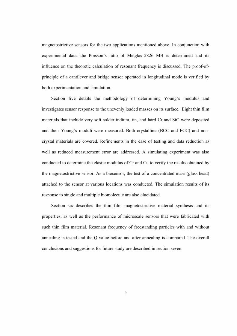
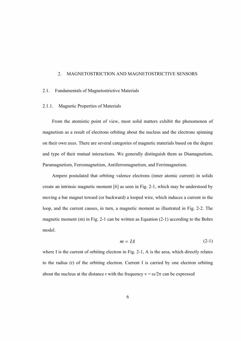
Ampere postulated that orbiting valence electrons (inner atomic current) in solids
create an intrinsic magnetic moment [6] as seen in Fig. 2-1, which may be understood by
moving a bar magnet toward (or backward) a looped wire, which induces a current in the
loop, and the current causes, in turn, a magnetic moment as illustrated in Fig. 2-2. The
magnetic moment (m) in Fig. 2-1 can be written as Equation (2-1) according to the Bohrs
model.
(2-1)
where I is the current of orbiting electron in Fig. 2-1, A is the area, which directly relates
to the radius (r) of the orbiting electron. Current I is carried by one electron orbiting
about the nucleus at the distance r with the frequency v = ω/2π can be expressed
IAm =
7
Fig. 2-1 Schematic showing the electrons orbiting around the nucleus to generate
magnetic moment.
S
NMagnet bar showing
magnetic field
DC current generated in coil by changing the magnetic field
Fig. 2-2 Schematic depicting the DC current generated in a closed circuit by moving
magnet field.
8
as:
(2-2)
where ω is the angular frequency. The orbiting magnetic moment is thus obtained via
Equation (2-3)
(2-3)
By a combination of the quantum mechanics and Bohrs model, the orbiting magnetic
moment must have the same value as Bohrs model, i.e.
(2-4)
This inner atomic current (electrons bound to their respective nuclei) can be influenced
by the external magnetic field, i.e. the applied magnetic field may accelerate or decelerate
the orbiting electrons. In addition, free electrons in metals are forced to move in a
magnetic field in a circular path, a so-called induced magnetic field. This induced field
tends to oppose the applied magnetic field. Diamagnetism is the characteristic of these
interactions of a matter with external magnetic field. All materials exhibit diamagnetic
response to an external magnetic field, but the magnitude and degree of such response is
generally very weak. An electron spinning on its own axis as a built-in angular
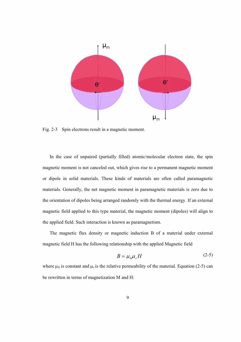
momentum with the value ħs also results in magnetic moment as illustrated in Fig. 2-3.
Here S is spin quantum number +/- 1/2, and ħ is the Planck constant with value of
6.626x10⁻³⁴ (J·S). In order to maintain the lowest energy state, based on Pauli principle,
the fully filled state, electrons spin in opposite directions in one electron state (one spins
up, another spins down), then the overall spin magnetic moment is zero as a result of their
canceling effect on each other, and diamagnetism is the only mannerism.
πω2
eI =
22
21
2reremorb ωπ
πω
==
)/(10274.9 24 TJmm Bohrorb−×==
9
Fig. 2-3 Spin electrons result in a magnetic moment.
In the case of unpaired (partially filled) atomic/molecular electron state, the spin
magnetic moment is not canceled out, which gives rise to a permanent magnetic moment
or dipole in solid materials. These kinds of materials are often called paramagnetic
materials. Generally, the net magnetic moment in paramagnetic materials is zero due to
the orientation of dipoles being arranged randomly with the thermal energy. If an external
magnetic field applied to this type material, the magnetic moment (dipoles) will align to
the applied field. Such interaction is known as paramagnetism.
The magnetic flux density or magnetic induction B of a material under external
magnetic field H has the following relationship with the applied Magnetic field
(2-5)
where µ0 is constant and µr is the relative permeability of the material. Equation (2-5) can
be rewritten in terms of magnetization M and H:
HB rµµ0=
10
(2-6)
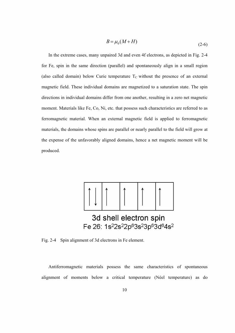
In the extreme cases, many unpaired 3d and even 4f electrons, as depicted in Fig. 2-4
for Fe, spin in the same direction (parallel) and spontaneously align in a small region
(also called domain) below Curie temperature TC without the presence of an external
magnetic field. These individual domains are magnetized to a saturation state. The spin
directions in individual domains differ from one another, resulting in a zero net magnetic
moment. Materials like Fe, Co, Ni, etc. that possess such characteristics are referred to as
ferromagnetic material. When an external magnetic field is applied to ferromagnetic
materials, the domains whose spins are parallel or nearly parallel to the field will grow at
the expense of the unfavorably aligned domains, hence a net magnetic moment will be
produced.
Fig. 2-4 Spin alignment of 3d electrons in Fe element.
Antiferromagnetic materials possess the same characteristics of spontaneous
alignment of moments below a critical temperature (Néel temperature) as do
)(0 HMB += µ
11
ferromagnetic materials. However, the neighboring atoms (sublattices) in
antiferromagnetic materials are aligned in antiparallel fashion, which results in a no net
magnetic moment. Cr, MnFe, and most ionic compounds, e.g. MnO, exhibit
antiferromagnetic properties. No particular applications of antiferromagnetic materials
have been found by employing the antiferromagnetism. In ferrimagnetic materials, the
magnetic moments are antiparallel like antiferromagnetic materials. The electrons of
neighboring atoms (sublattices) are arranged in the opposite direction, but the magnetic
moments are not equal or not completely cancelled out; consequently, a net magnetic
moment is produced.
2.1.2. Magnetostrictive Behavior and Magnetoelastic Interactions of Magnetic
Materials
Most ferromagnetic materials exhibit the magnetostrictive phenomenon, that is, the
material changes in dimension as a result of the domains aligning to an applied external
magnetic field. This effect was first observed with Ni and Fe material in 1842, by James
Joule [7, 8]. In fact, with this change in dimension, the magnetization state in the material
is hence changed, which interacts with the external field and results in magnetoelastic
behavior.
As discussed in the previous section, ferrimagnetic and antiferromagnetic materials
also possess the same magnetostriction behavior as ferromagnetic materials.
Ferromagnetic materials generally are Fe, Ni, and Co metals or their alloys.
Ferrimagnetic materials, however, are ceramics and anisotropic and usually exhibit the
hard magnetic properties of large remanence and coercive field. Antiferromagnetic
12
materials are most commonly found among ionic compounds and have no particular
applications. So far, ferromagnetic materials have been demonstrated to be a good
candidate for magnetostrictive sensors because of their soft magnetic properties (low
remanence and coercive field) in general. Moreover, ferromagnetic material can be made
in amorphous (non-crystalline) metallic alloys by rapidly spinning and cooling of a liquid
alloy [9]. For example, Metglas 2826 MB [10], consisting of Fe, Ni, Mo, and B, is a
typical amorphous ferromagnetic material having the advantages of nearly magnetic
isotropic structure, considerable high permeability, low coercivity, and low hysteresis
loss. Therefore, in this research, we are interested in the ferromagnetic materials
including Fe, Ni, Co and their alloys, in particular, Metglas with Fe40Ni38Mo4B18 in
ribbon and sputtered film forms. Metglas 2826 MB is used as the prototype material for
fabrication of sensors in bulk-scale and as the sputtering target for deposition of
magnetostrictive thin films that are used to fabricate microscale sensor platforms.
The most common and well developed magnetostrictive sensors are designed to
measure the linear displacement and strain [11, 12], which is based on the
magnetostrictive behavior of magnetostrictive material. The application of
magnetostrictive sensors to measure chemical or biochemical agents as a mass sensor has
only been conducted in recent years [13-25]. The operation principle of such sensors is
completely different from that which is used as a mechanical sensor to measure the linear
displacement or strain. If a magnetostrictive material is exposed to an alternating
magnetic field, it is subjected to compression and extension in the longest axis;
subsequently the applied field will be interacted by such a change of inner state of
magnetization. When the frequency of the alternating magnetic field is equal to the
13
magnetostrictive material’s resonant frequency, the largest oscillation will occur. As a
result, the highest magnetic flux density is produced, and the resonant frequency can be
detected by analysis of the signal in a close loop circuit. This is the basis for antitheft
sensor tags currently used Electronic Article Surveillance (EAS) system [26, 27] and
sensors used to measure chemical and biochemical species.
This study will further extend the applications of the magnetostrictive phenomena to
measuring Young’s modulus of thin film material and detecting mass loaded on
magnetostrictive sensors.
2.2. Magnetostrictive Sensor Operation in the Longitudinal Vibration Mode
When the alternating magnetic field is applied to a sensor that is made of
magnetostrictive material in a rectangular shape, with the easy magnetization axis aligned
with the longitudinal direction, it can cause the sensor to oscillate in its resonant
frequency. Here, the magnetic energy is transferred to mechanical energy to cause the
sensor to change its shape (dimension) as a result of switching domains in the
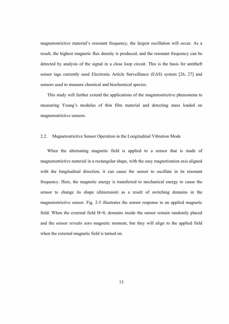
magnetostrictive sensor. Fig. 2-5 illustrates the sensor response to an applied magnetic
field. When the external field H=0, domains inside the sensor remain randomly placed
and the sensor reveals zero magnetic moment, but they will align to the applied field
when the external magnetic field is turned on.
14
Fig. 2-5 Schematics of a magnetostrictive sensor’s response to the applied magnetic
field.
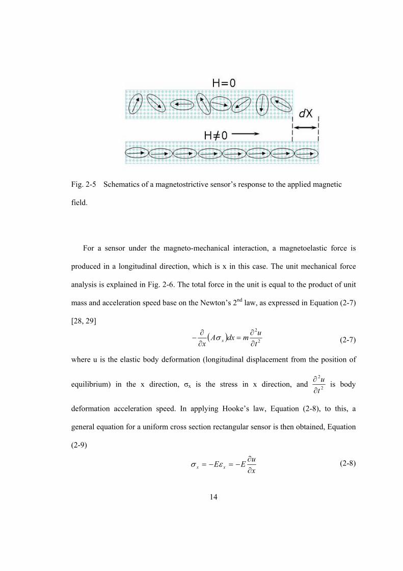
For a sensor under the magneto-mechanical interaction, a magnetoelastic force is
produced in a longitudinal direction, which is x in this case. The unit mechanical force
analysis is explained in Fig. 2-6. The total force in the unit is equal to the product of unit
mass and acceleration speed base on the Newton’s 2nd law, as expressed in Equation (2-7)
[28, 29]
(2-7)
where u is the elastic body deformation (longitudinal displacement from the position of
equilibrium) in the x direction, σx is the stress in x direction, and 2
2
tu
∂∂ is body
deformation acceleration speed. In applying Hooke’s law, Equation (2-8), to this, a
general equation for a uniform cross section rectangular sensor is then obtained, Equation
(2-9)
(2-8)
( ) 2
2
tumdxA
x x ∂∂
=∂∂
− σ
xuEE xx ∂∂
−=−= εσ
15
(2-9)
where u is the elastic body deformation (displacement) in x direction, and xu∂∂ , 2
2
xu
∂∂ are
the strain and strain rate, respectively. E and ρ correspondingly denote the Young’s
modulus and density of the sensor material. Young’s modulus E expressed here is
dependent on the state of strain in the structure. The elastic body deformation
(displacement) u should be such a function of x and (time) t as to satisfy the partial
differential of Equation (2-9).
Fig. 2-6 Mechanical force analysis in a unit of sensor.
2
2
2
2
xuE
tu
∂∂
⎟⎟⎠
⎞⎜⎜⎝
⎛=
∂∂
ρ
16
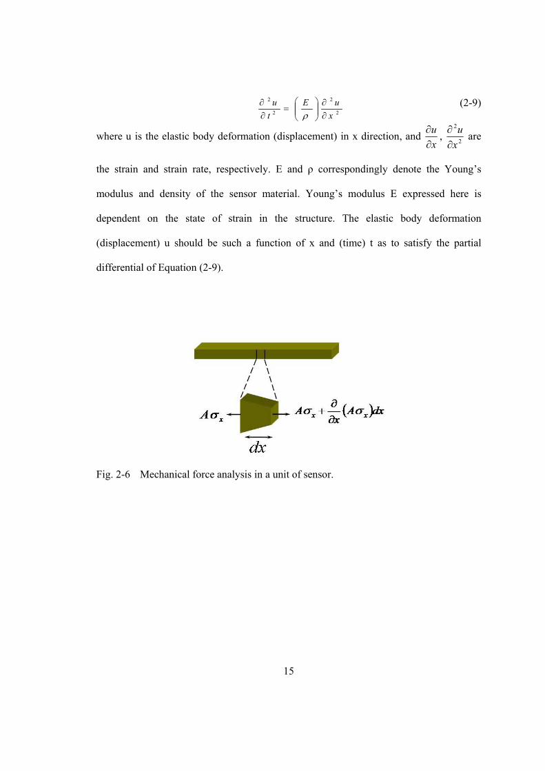
2.2.1. Fix-Free Ended Cantilever Sensor
When a fix-free ended structure sensor (Fig. 2-7), thereafter called cantilever, is
actuated in the longitudinal vibration mode, the natural frequency can be obtained by
applying the boundary conditions of
0)( 0 ==xu
and
0=⎟⎠⎞
⎜⎝⎛∂∂
=Lxxu
to Equation (2-9), and the resonant frequency in longitudinal vibration mode without
considering the damping effect is obtained as following equation
(2-10)
where n is integral, equals to 1, 2, 3…., for the first mode, n = 1. L is the length of the
sensor.
Fig. 2-7 Schematic showing a fix-free ended cantilever with L(length)>W(width).
ρE
Lnf4
12 −=
17
2.2.2. Fix-Fix and Free-Free Ended Sensors
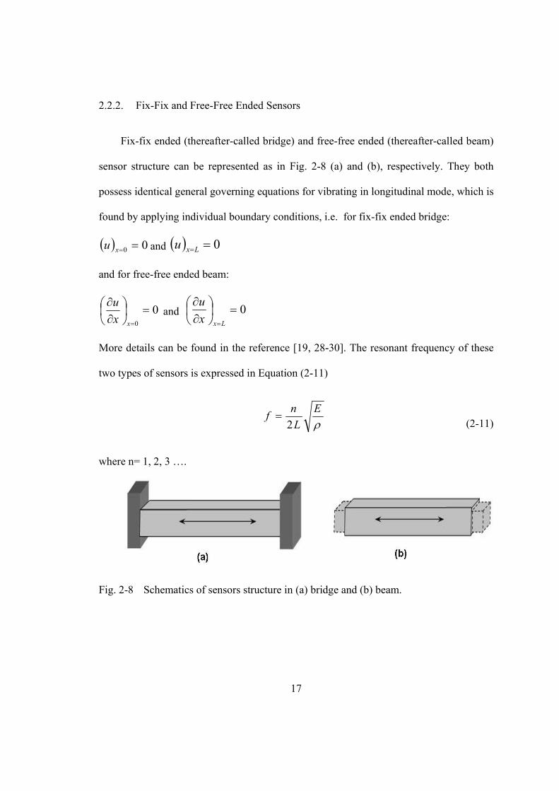
Fix-fix ended (thereafter-called bridge) and free-free ended (thereafter-called beam)
sensor structure can be represented as in Fig. 2-8 (a) and (b), respectively. They both
possess identical general governing equations for vibrating in longitudinal mode, which is
found by applying individual boundary conditions, i.e. for fix-fix ended bridge:
( ) 00 ==xu and ( ) 0==Lxu
and for free-free ended beam:
00
=⎟⎠⎞
⎜⎝⎛∂∂
=xxu
and 0=⎟⎠⎞
⎜⎝⎛∂∂
=Lxxu
More details can be found in the reference [19, 28-30]. The resonant frequency of these
two types of sensors is expressed in Equation (2-11)
(2-11)
where n= 1, 2, 3 ….
Fig. 2-8 Schematics of sensors structure in (a) bridge and (b) beam.
ρE
Lnf
2=
18
One can see that the resonant frequency magnitudes for the bridge and beam type
sensor are twice that of the cantilever type. Additionally, the frequency is only dependent
on the material’s intrinsic properties and geometry of length.
2.3. Application of Magnetostrictive Sensors
Assuming that there is a solid, continuous thin film firmly deposited onto the sensor’s
surface, the resonant frequency of the sensor will consequently be shifted up or down,
dependent on the shifts of elastic modulus and density. The change in frequency for any
type of sensor described above can be approximately estimated by the first order Taylor
expression
(2-12)
where ∆f, ∆E and ∆ρ are the change of frequency, effective Young’s modulus, and
effective density of the sensor due to the thin film coating deposition, respectively. f0 is
the frequency of a sensor without any coating. In the case of no coating, the effective
modulus and density will be the sensor material itself. When a sensor is deposited with a
thin film coating, the effective modulus and effective density will be determined from
both sensor and film materials.
It is possible to measure the thin film’s Young’s modulus by knowing the sensor
material’s properties. Grimes and his coworkers demonstrated this possibility of
measuring the elastic modulus of Ag and Al thin films [31, 32]. If the coating has the
same Young’s modulus and density as the sensor does, there will be no change in
021 f
EEf ⎟⎟
⎠
⎞⎜⎜⎝
⎛ ∆−
∆=∆
ρρ
19
frequency. However, if the film coating is evenly deposited on the surface without
change the elastic modulus of this structure, Equation (2-12), can be written as
(2-13)
This equation can be further written as Equation (2-14) if there is a mass evenly
distributed on the sensor surface.
(2-14)
This is the foundation of employing a resonated sensor in detecting the presence of a
chemical or biochemical mass attaching to its surface.
2.3.1. Mechanical Sensor for Measuring Young’s Modulus of Thin Film Material
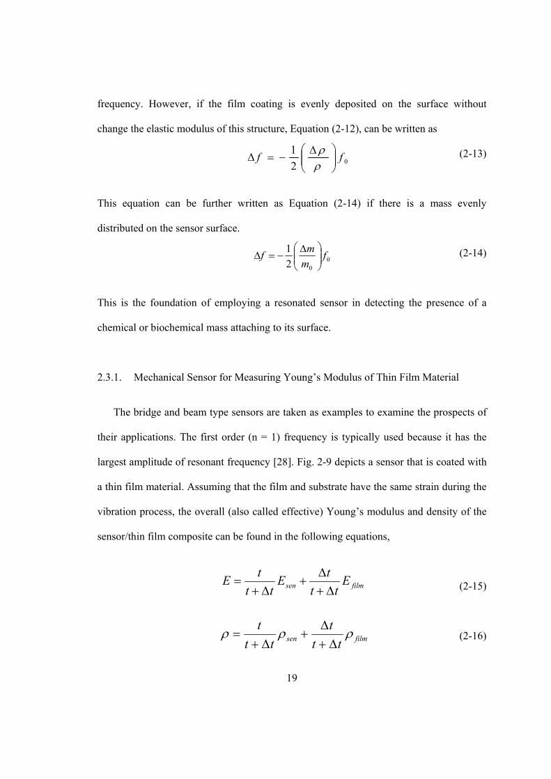
The bridge and beam type sensors are taken as examples to examine the prospects of
their applications. The first order (n = 1) frequency is typically used because it has the
largest amplitude of resonant frequency [28]. Fig. 2-9 depicts a sensor that is coated with
a thin film material. Assuming that the film and substrate have the same strain during the
vibration process, the overall (also called effective) Young’s modulus and density of the
sensor/thin film composite can be found in the following equations,
(2-15)
(2-16)
filmsen Ett
tEtt
tE∆+
∆+
∆+=
filmsen ttt
ttt ρρρ
∆+∆
+∆+
=
021 ff ⎟⎟
⎠
⎞⎜⎜⎝
⎛ ∆−=∆
ρρ
002
1 fm
mf ⎟⎟⎠
⎞⎜⎜⎝
⎛ ∆−=∆
20
where subscripts sen and film denote the sensor and thin film, respectively. parameters t
and ∆t are the thickness of sensor and the film, respectively.
Fig. 2-9 Representation of sensor with thin layer of coating [33].
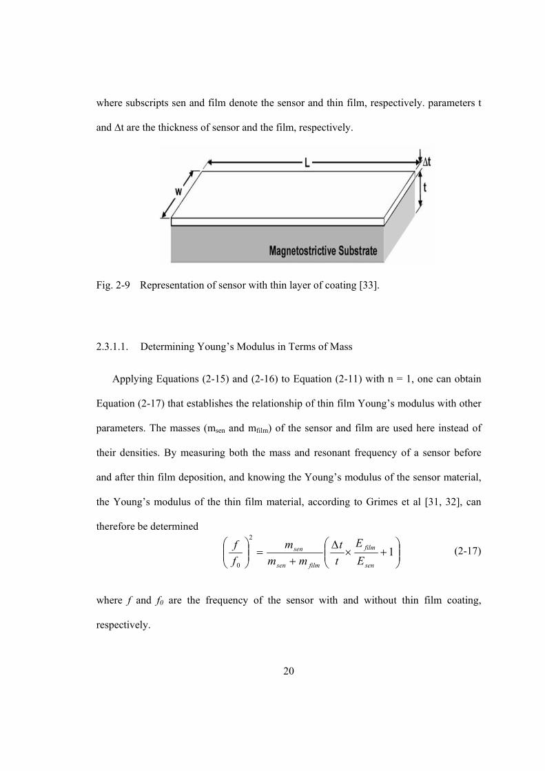
2.3.1.1. Determining Young’s Modulus in Terms of Mass
Applying Equations (2-15) and (2-16) to Equation (2-11) with n = 1, one can obtain
Equation (2-17) that establishes the relationship of thin film Young’s modulus with other
parameters. The masses (msen and mfilm) of the sensor and film are used here instead of
their densities. By measuring both the mass and resonant frequency of a sensor before
and after thin film deposition, and knowing the Young’s modulus of the sensor material,
the Young’s modulus of the thin film material, according to Grimes et al [31, 32], can
therefore be determined
(2-17)
where f and f0 are the frequency of the sensor with and without thin film coating,
respectively.
⎟⎟⎠
⎞⎜⎜⎝
⎛+×
∆+
=⎟⎟⎠
⎞⎜⎜⎝
⎛1
2
0 sen
film
filmsen
sen
EE
tt
mmm
ff
21
2.3.1.2. Determining Young’s Modulus in Terms of Density
Applying Equations (2-15) and (2-16) to Equation (2-12), one can rewrite Equation
(2-12) as
(2-18)
As it can be seen, if assuming the thin film Young’s modulus and its density are thickness
independent under the micro scale regime, the relative resonant frequency shift 0ff∆ is a
linear function of the relative film thickness changett
t∆+
∆ . The thin film Young’s
modulus can therefore be determined. This method requires the measuring density of thin
film that is typically identical to its bulk value and has the potential to provide more
accurate results.
2.3.1.3. Error Analysis
Two methodologies of determining the Young’s modulus of thin film coating have
been described, which theoretically should give an identical result. However, the
resolution for each instrument may vary; hence, a relative measurement error may occur.
The error can be derived from Equations (2-17) and (2-18) and expressed in Equations
(2-19) and (2-20). The error in measuring mass is eliminated in the second equation.
⎟⎟⎠
⎞⎜⎜⎝
⎛−⎟
⎠⎞
⎜⎝⎛
∆+∆
=∆
sen
film
sen
film
EE
ttt
ff
ρρ
21
0
fff −=∆ 0
22
(2-19)
(2-20)
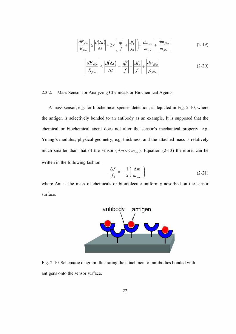
2.3.2. Mass Sensor for Analyzing Chemicals or Biochemical Agents
A mass sensor, e.g. for biochemical species detection, is depicted in Fig. 2-10, where
the antigen is selectively bonded to an antibody as an example. It is supposed that the
chemical or biochemical agent does not alter the sensor’s mechanical property, e.g.
Young’s modulus, physical geometry, e.g. thickness, and the attached mass is relatively
much smaller than that of the sensor ( senmm <<∆ ). Equation (2-13) therefore, can be
written in the following fashion
(2-21)
where ∆m is the mass of chemicals or biomolecule uniformly adsorbed on the sensor
surface.
Fig. 2-10 Schematic diagram illustrating the attachment of antibodies bonded with
antigens onto the sensor surface.
( )film
film
sen
sen
film
film
mdm
mdm
fdf
fdf
ttd
EdE
++⎟⎟⎠
⎞⎜⎜⎝
⎛+×+
∆∆
≤0
02
( )film
film
film
film df
dff
dfttd
EdE
ρρ
+++∆∆
≤0
0
⎟⎟⎠
⎞⎜⎜⎝
⎛ ∆−=
∆
senmm
ff
21
0
23
Sensor sensitivity, which is a key characteristic of a mass sensor, is defined as “the
resonant frequency change per mass change”, written as
(2-22)
This is the general equation for all types of sensors discussed previously. From this it is
clear that a higher sensitivity can be obtained by reducing the sensor’s mass and making
it more comparable to the target mass, e.g. constructing micro scale sensor platforms.
2.3.2.1. Mass Sensor with Uniformly Distributed Mass Attachment
The first order natural frequency of a cantilever sensor found from Equation (2-10) is
expressed in Equation (2-23)
(2-23)
The change in resonant frequency due to a uniformly distributed mass load on the sensor
is stated as
(2-24)
Similarly, the first order natural frequency for the bridge and beam sensor is obtained
from Equation (2-11) and is given by Equation (2-25)
(2-25)
The change in the resonant frequency due to a uniformly distributed mass load on the
sensor is expressed in Equation (2-26).
senmf
mfS
20=
∆∆
=
ρE
Lf
41
0 =
ρE
mm
Lf
mmf
sensen⎟⎟⎠
⎞⎜⎜⎝
⎛ ∆−=⎟⎟
⎠
⎞⎜⎜⎝
⎛ ∆−=∆
81
21
0
ρE
Lf
21
0 =
24
(2-26)
For a sensor of the same size, a bridge or beam sensor yields a value of frequency and
sensitivity two times greater than that for a cantilever sensor. One may see the higher
sensitivity is attainable from the benefits of using
• Bridge and beam type sensors, and
• Microscale geometry, as a result of reduction of the sum of mass.
2.3.2.2. Mass Sensor with a Concentrated Mass Attachment
The resonant frequency shift of a sensor due to a uniform mass distribution on the
sensor surface was described in Equations (2-24) and (2-26). However, if the mass is not
evenly loaded on the sensor surface, e.g. a single biomolecule cell, the sensor’s response
to such concentrated mass will be different. Fig. 2-11 depicts a cantilever sensor with a
concentrated mass attached at the free end. Recall the differential Equation (2-9),
The boundary conditions for the case of a concentrated mass attached to the free end of a
cantilever are [29]:
at x = 0,
(2-27)
and at x = L,
(2-28)
ρE
mm
Lf
mmf
sensen⎟⎟⎠
⎞⎜⎜⎝
⎛ ∆−=⎟⎟
⎠
⎞⎜⎜⎝
⎛ ∆−=∆
41
21
0
2
2
2
2
xuE
tu
∂∂
⎟⎟⎠
⎞⎜⎜⎝
⎛=
∂∂
ρ
( )xuEA
tum
∂∂
−=⎟⎟⎠
⎞⎜⎜⎝
⎛∂∂
∆ 2
2
0=u
25
L
x
y
Fig. 2-11 Schematic diagram showing the concentrated mass attached to the free end
of a cantilever.
Assuming that the cantilever performs one of the principal modes of vibration, the u,
therefore, can be expressed as a function of x and t in Equation (2-29)
(2-29)
in which A and B are constants, f(x) is a certain function of x alone, and β is the angular
frequency of this vibrating system. By submitting Equation (2-29) to Equation (2-9), one
can obtain,
(2-30)
The boundary conditions of Equations (2-27) and (2-28), therefore, become
(2-31)
and
(2-32)
[ ])sin()cos()(),( tBtAxftxu ββ +=
0)()(2
=+′′ xfE
xf ρβ
0)0( =f
0)()( 2 =⎟⎠⎞
⎜⎝⎛ ∆−′ Lf
EAmLf β
26
Let η be the ratio of the attached mass (∆m) to the mass of the cantilever (msen = ALρ),
and inserting
ρη
ALm
mm
sen
∆=
∆=
into Equation (2-32), we have
(2-33)
The standard solution to Equation (2-30) is
(2-34)
To satisfy the boundary condition: 0)0( =f , C must vanish and β must be real. Equation
(2-34) therefore becomes
(2-35)
To meet the boundary condition of Equation (2-33), Equation (2-35) becomes
(2-36)
Let E
k ρβ= , then Equation (2-36) can be written as
(2-37)
It is clear that the solution to Equation (2-37) is directly related to the value of η. If η = 0,
it means there is no mass attached on the free end, the solution for Equation (2-37) will
be kL = (2n-1)π/2, n = 1.2,3…, in fact, this is the case of fix-free ended cantilever. The
0)()(2
=⎟⎟⎠
⎞⎜⎜⎝
⎛−′ Lf
ELLf ρβη
)sin()cos()( xE
DxE
Cxf ρβρβ +=
)sin()( xE
Dxf ρβ=
kLkL
η1)tan( =
)sin()()cos(E
LE
LE
L ρβρβηρβ =
27
resonant frequency of this cantilever system can be obtained and expressed in Equation
(2-38), which is the same as Equation (2-10).
(2-38)
where n = 1, 2, 3,…
Similarly, if η is infinitely large, which means the mass attached on the free end is too
large, the system, therefore, corresponds to a fixed end at x = L, or fix-fix ended bridge.
In such case, the solution for Equation (2-37) is
kL = nπ, n = 0, 1, 2, 3,…
Then the resonant frequency of such system is expressed in Equation (2-39), which is
equivalent to Equation (2-11)
(2-39)
where n = 1, 2, 3,…
The general resonant frequency for a cantilever with a concentrated mass attached at the
free end is expressed as following,
(2-40)
Now we consider the case of attaching a small amount of mass on the free end, for
example, if η = 0.0005, the approximate solution to Equation (2-36) is kL = 1.570019.
The resonant frequency for this case is
ρπρ
π
πβ E
Ln
EL
n
f4
122
2)12(
2−
=
−
==
ρπρ
π
πβ E
Ln
EL
n
f222
===
ρππρ
πβ Ek
Ekf
222===
28
(2-41)
The resonant frequency shift due to this concentrated mass (∆m = 0.0005msen) attached to
the free end can be obtained as the following:
(2-42)
The relative frequency change is then
4
0
1094861607.41140038.3 −×−=⎟⎠⎞
⎜⎝⎛ −=
∆πf
f
If we consider that this amount of mass (∆m) is uniformly distributed on the sensor’s
surface, then the relative frequency change can be obtained from Equation (2-21) and is,
We can see that the concentrated mass attached on the free end has much higher
frequency change than the uniformly distributed one. Similarly, it is easy to determine
that there will be no change in resonant frequency if the concentrated mass is attached to
the fixed end of a cantilever or bridge.
For different ratios (η values) of the concentrated mass to the mass of this cantilever
sensor, the solution (kL value) of Equation (2-37) can be either mathematically or
graphically obtained. Table 2-1 lists the kL values for some particular η values for the
fundamental mode (n = 1).
4
0
105.20005.021
21 −×−=×−=⎟⎟
⎠
⎞⎜⎜⎝
⎛ ∆−=
∆
senmm
ff
ρππρ
πρ
πβ E
L
EL
Ekf
2570019.1
2
570019.1
22====
00 1140038.3411
2
570019.141
2570019.1 fE
LE
LE
Lfff ⎟
⎠⎞
⎜⎝⎛ −=⎟⎟
⎠
⎞⎜⎜⎝
⎛
⎟⎟⎟⎟
⎠
⎞
⎜⎜⎜⎜
⎝
⎛
−=−=−=∆πρπρρπ
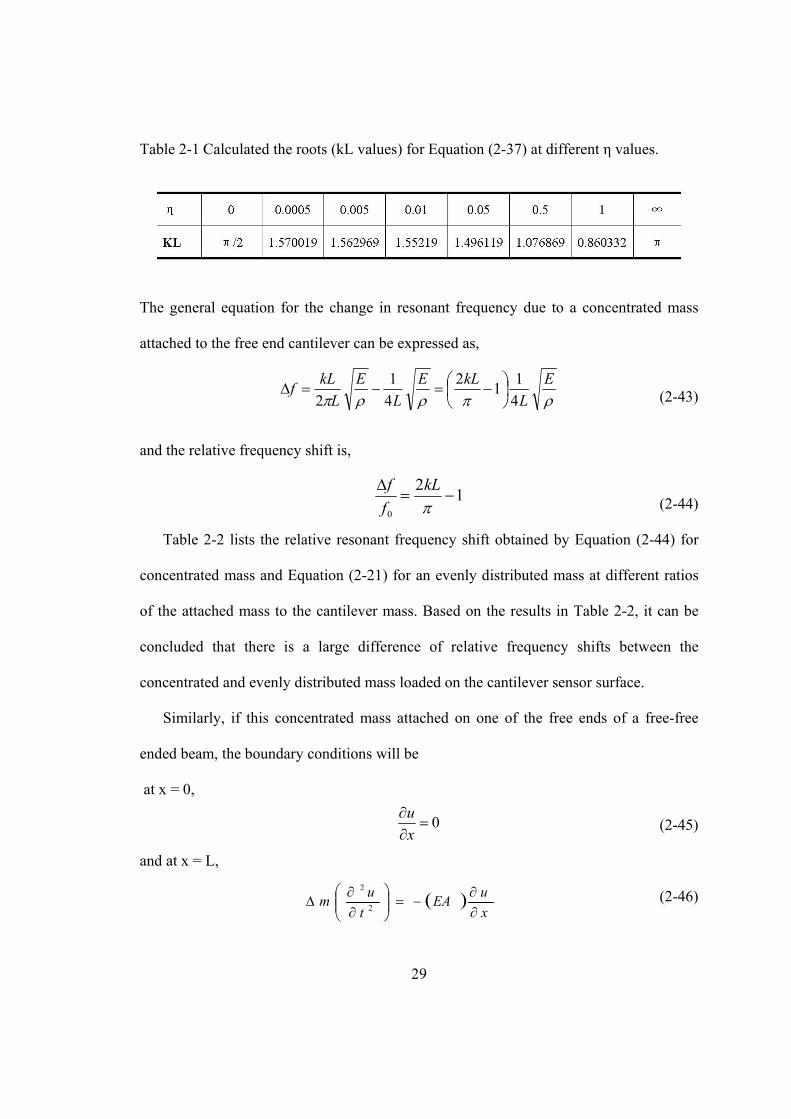
29
Table 2-1 Calculated the roots (kL values) for Equation (2-37) at different η values.
The general equation for the change in resonant frequency due to a concentrated mass
attached to the free end cantilever can be expressed as,
(2-43)
and the relative frequency shift is,
(2-44)
Table 2-2 lists the relative resonant frequency shift obtained by Equation (2-44) for
concentrated mass and Equation (2-21) for an evenly distributed mass at different ratios
of the attached mass to the cantilever mass. Based on the results in Table 2-2, it can be
concluded that there is a large difference of relative frequency shifts between the
concentrated and evenly distributed mass loaded on the cantilever sensor surface.
Similarly, if this concentrated mass attached on one of the free ends of a free-free
ended beam, the boundary conditions will be
at x = 0,
(2-45)
and at x = L,
(2-46)
ρπρρπE
LkLE
LE
LkLf
4112
41
2⎟⎠⎞
⎜⎝⎛ −=−=∆
12
0
−=∆
πkL
ff
( )xuEA
tum
∂∂
−=⎟⎟⎠
⎞⎜⎜⎝
⎛∂∂
∆ 2
2
0=∂∂
xu
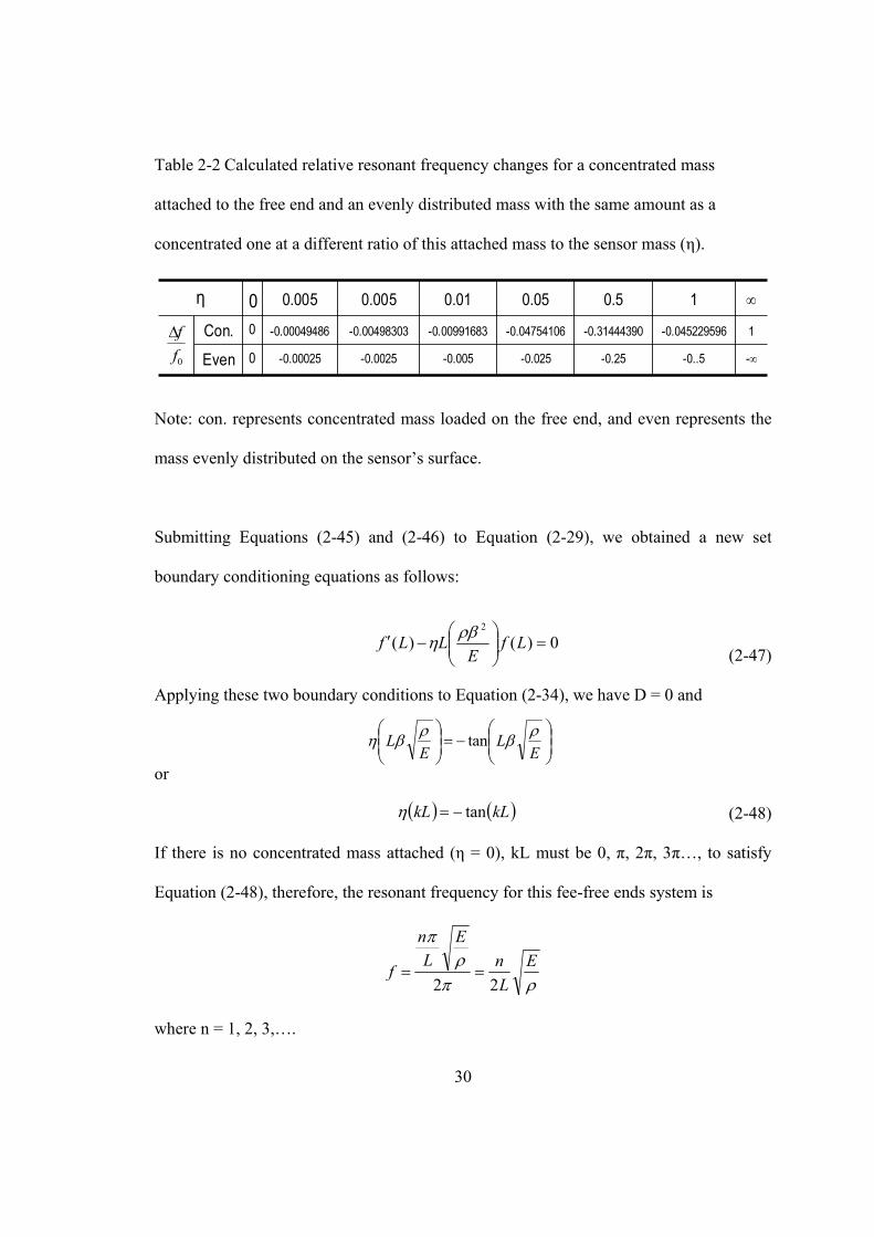
30
Table 2-2 Calculated relative resonant frequency changes for a concentrated mass
attached to the free end and an evenly distributed mass with the same amount as a
concentrated one at a different ratio of this attached mass to the sensor mass (η).
-∞
1
∞
-0..5
-0.045229596
1
-0.25
-0.31444390
0.5
-0.025
-0.04754106
0.05
-0.005
-0.00991683
0.01
-0.0025
-0.00498303
0.005
-0.00025
-0.00049486
0.005
0
0
0
Even
Con.
η
0ff∆
Note: con. represents concentrated mass loaded on the free end, and even represents the
mass evenly distributed on the sensor’s surface.
Submitting Equations (2-45) and (2-46) to Equation (2-29), we obtained a new set
boundary conditioning equations as follows:
(2-47)
Applying these two boundary conditions to Equation (2-34), we have D = 0 and
or
(2-48)
If there is no concentrated mass attached (η = 0), kL must be 0, π, 2π, 3π…, to satisfy
Equation (2-48), therefore, the resonant frequency for this fee-free ends system is
ρπρ
πE
Ln
EL
n
f22
==
where n = 1, 2, 3,….
0)()(2
=⎟⎟⎠
⎞⎜⎜⎝
⎛−′ Lf
ELLf ρβη
⎟⎟⎠
⎞⎜⎜⎝
⎛−=⎟⎟
⎠
⎞⎜⎜⎝
⎛
EL
EL ρβρβη tan
( ) ( )kLkL tan−=η
31
If η is infinitely large, the solution to Equation (2-48) is kL = π/2, 3π/2, 5π/2, and the
resonant frequency of this system is
ρπρ
πE
Ln
EL
n
f4
122
2)12(
−=
−
=
In fact, this system is identical to fix-free ended cantilever in this case.
The general resonant frequency equation for this free-free ended beam with a
concentrated mass attached to one of its ends is actually the same as the case of the
cantilever attached with a concentrated mass on the free end as stated by Equation (2-40).
The difference is that the k value is different due to boundary conditions different in
particular case. However, the relative frequency shift for the free-free ended beam system
is as following:
(2-49)
Table 2-3 lists the solution of kL value for Equation (4-48) and the relative resonant
frequency shift for some particular η values. If there is no concentrated mass attached on
the end, there is no frequency change. If the attached mass is infinitely large, the resonant
frequency is reduced to the half of that for the free-free ended beam system, which is
identical to the case of fix-free ended cantilever. It can be seen that the relative frequency
shift for a concentrated mass attached to one end of the freestanding beam is also higher
than that of evenly distributed mass on the sensor surface.
10
−=∆
πkL
ff
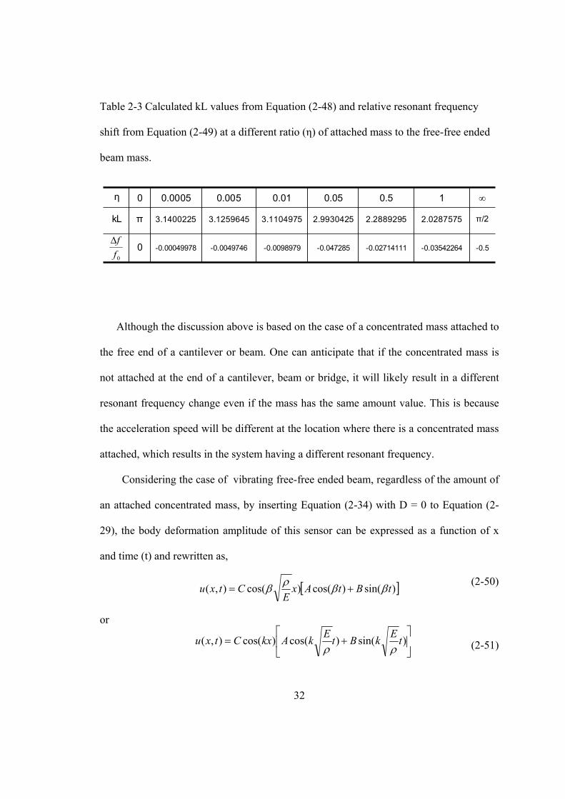
32
Table 2-3 Calculated kL values from Equation (2-48) and relative resonant frequency
shift from Equation (2-49) at a different ratio (η) of attached mass to the free-free ended
beam mass.
-0.5
π/2
∞
-0.03542264
2.0287575
1
-0.02714111
2.2889295
0.5
-0.047285
2.9930425
0.05
-0.0098979
3.1104975
0.01
-0.0049746
3.1259645
0.005
-0.00049978
3.1400225
0.0005
0
π
0
kL
η
0ff∆
Although the discussion above is based on the case of a concentrated mass attached to
the free end of a cantilever or beam. One can anticipate that if the concentrated mass is
not attached at the end of a cantilever, beam or bridge, it will likely result in a different
resonant frequency change even if the mass has the same amount value. This is because
the acceleration speed will be different at the location where there is a concentrated mass
attached, which results in the system having a different resonant frequency.
Considering the case of vibrating free-free ended beam, regardless of the amount of
an attached concentrated mass, by inserting Equation (2-34) with D = 0 to Equation (2-
29), the body deformation amplitude of this sensor can be expressed as a function of x
and time (t) and rewritten as,
(2-50)
or
(2-51)
[ ])sin()cos()cos(),( tBtAxE
Ctxu ββρβ +=
⎥⎦
⎤⎢⎣
⎡+= )sin()cos()cos(),( tEkBtEkAkxCtxu
ρρ
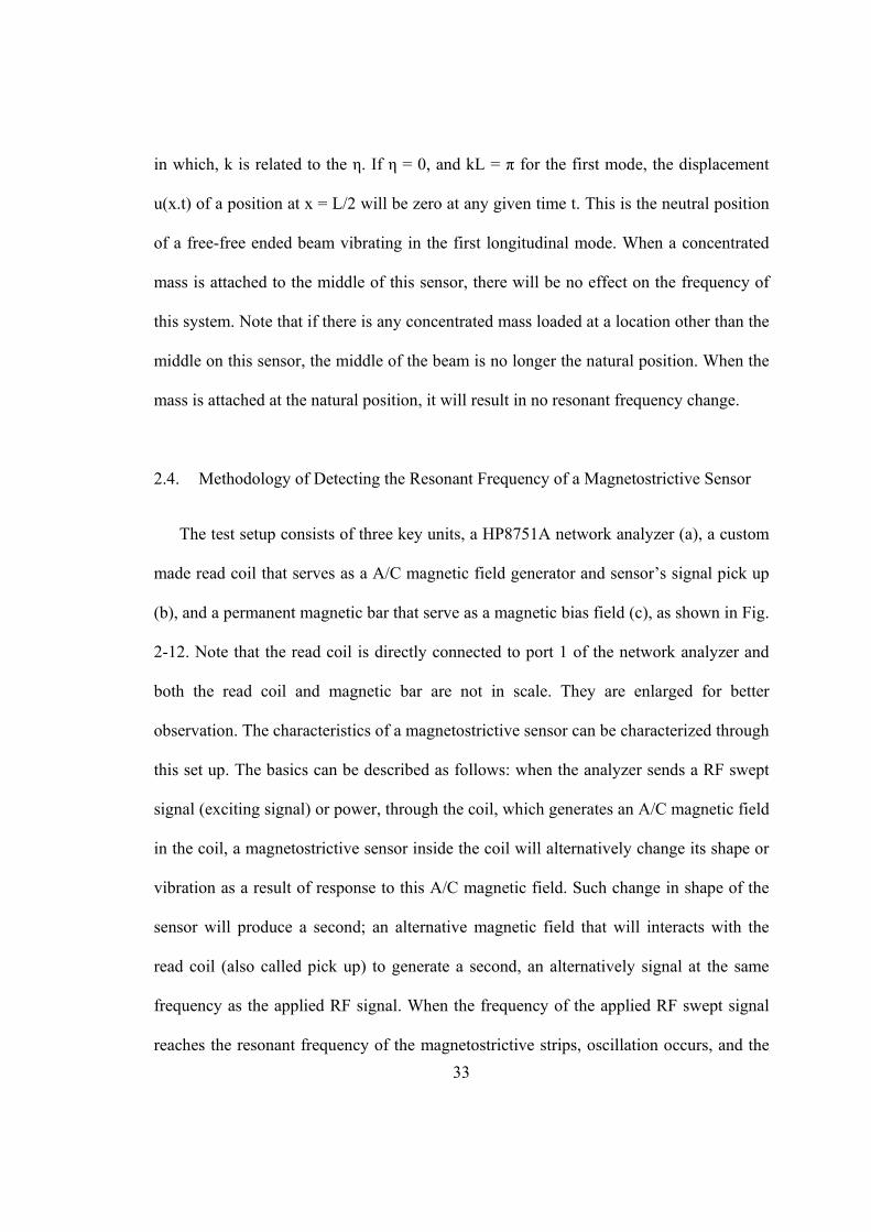
33
in which, k is related to the η. If η = 0, and kL = π for the first mode, the displacement
u(x.t) of a position at x = L/2 will be zero at any given time t. This is the neutral position
of a free-free ended beam vibrating in the first longitudinal mode. When a concentrated
mass is attached to the middle of this sensor, there will be no effect on the frequency of
this system. Note that if there is any concentrated mass loaded at a location other than the
middle on this sensor, the middle of the beam is no longer the natural position. When the
mass is attached at the natural position, it will result in no resonant frequency change.
2.4. Methodology of Detecting the Resonant Frequency of a Magnetostrictive Sensor
The test setup consists of three key units, a HP8751A network analyzer (a), a custom
made read coil that serves as a A/C magnetic field generator and sensor’s signal pick up
(b), and a permanent magnetic bar that serve as a magnetic bias field (c), as shown in Fig.
2-12. Note that the read coil is directly connected to port 1 of the network analyzer and
both the read coil and magnetic bar are not in scale. They are enlarged for better
observation. The characteristics of a magnetostrictive sensor can be characterized through
this set up. The basics can be described as follows: when the analyzer sends a RF swept
signal (exciting signal) or power, through the coil, which generates an A/C magnetic field
in the coil, a magnetostrictive sensor inside the coil will alternatively change its shape or
vibration as a result of response to this A/C magnetic field. Such change in shape of the
sensor will produce a second; an alternative magnetic field that will interacts with the
read coil (also called pick up) to generate a second, an alternatively signal at the same
frequency as the applied RF signal. When the frequency of the applied RF swept signal
reaches the resonant frequency of the magnetostrictive strips, oscillation occurs, and the
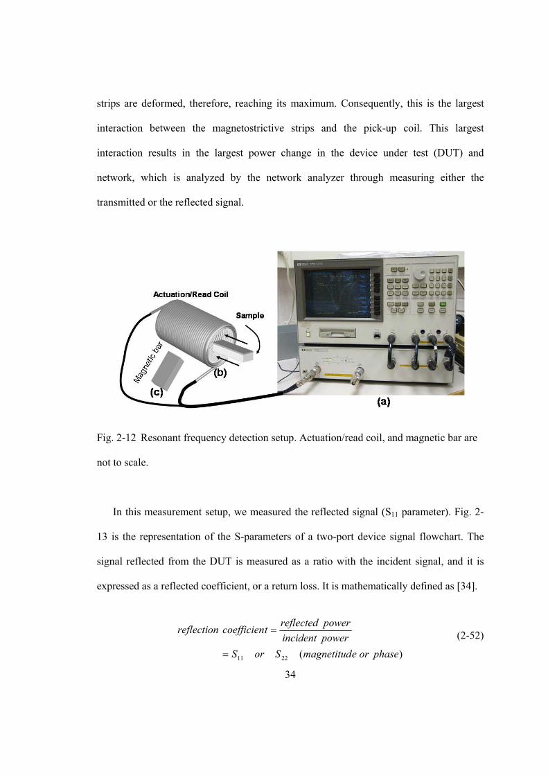
34
strips are deformed, therefore, reaching its maximum. Consequently, this is the largest
interaction between the magnetostrictive strips and the pick-up coil. This largest
interaction results in the largest power change in the device under test (DUT) and
network, which is analyzed by the network analyzer through measuring either the
transmitted or the reflected signal.
Fig. 2-12 Resonant frequency detection setup. Actuation/read coil, and magnetic bar are
not to scale.
In this measurement setup, we measured the reflected signal (S11 parameter). Fig. 2-
13 is the representation of the S-parameters of a two-port device signal flowchart. The
signal reflected from the DUT is measured as a ratio with the incident signal, and it is
expressed as a reflected coefficient, or a return loss. It is mathematically defined as [34].
(2-52)
)(2211 phaseoremagnetitudSorSpowerincidentpowerreflectedtcoefficienreflection
=
=
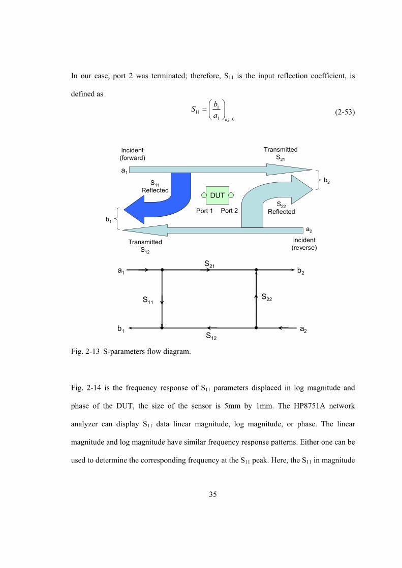
35
In our case, port 2 was terminated; therefore, S11 is the input reflection coefficient, is
defined as
(2-53)
S11Reflected
S22Reflected
a1
a2
Incident(forward)
Incident(reverse)
b1
TransmittedS12
TransmittedS21
b2
DUT
Port 1 Port 2
a1
b1
b2
a2
S11
S12
S21
S22
Fig. 2-13 S-parameters flow diagram.
Fig. 2-14 is the frequency response of S11 parameters displaced in log magnitude and
phase of the DUT, the size of the sensor is 5mm by 1mm. The HP8751A network
analyzer can display S11 data linear magnitude, log magnitude, or phase. The linear
magnitude and log magnitude have similar frequency response patterns. Either one can be
used to determine the corresponding frequency at the S11 peak. Here, the S11 in magnitude
01
111
2=⎟⎟⎠
⎞⎜⎜⎝
⎛=
aabS
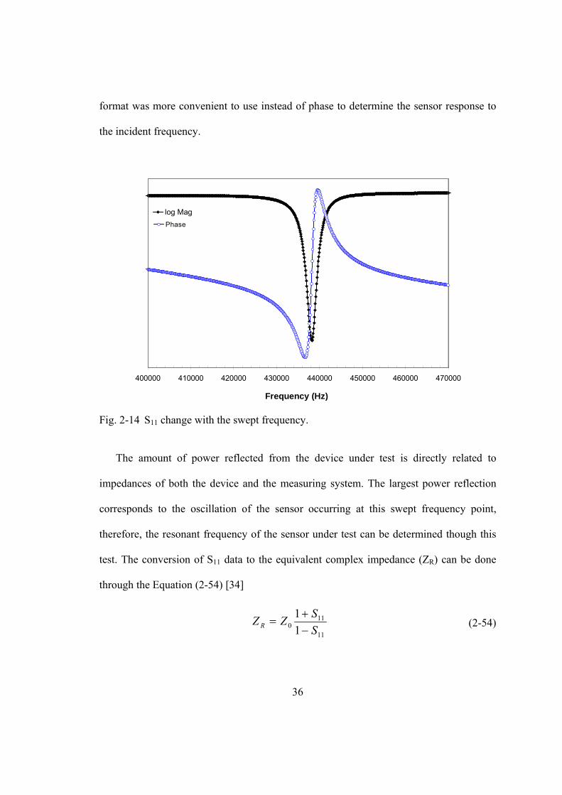
36
format was more convenient to use instead of phase to determine the sensor response to
the incident frequency.
400000 410000 420000 430000 440000 450000 460000 470000
log MagPhase
Frequency (Hz)
Fig. 2-14 S11 change with the swept frequency.
The amount of power reflected from the device under test is directly related to
impedances of both the device and the measuring system. The largest power reflection
corresponds to the oscillation of the sensor occurring at this swept frequency point,
therefore, the resonant frequency of the sensor under test can be determined though this
test. The conversion of S11 data to the equivalent complex impedance (ZR) can be done
through the Equation (2-54) [34]
(2-54)
11
110 1
1SSZZ R −
+=
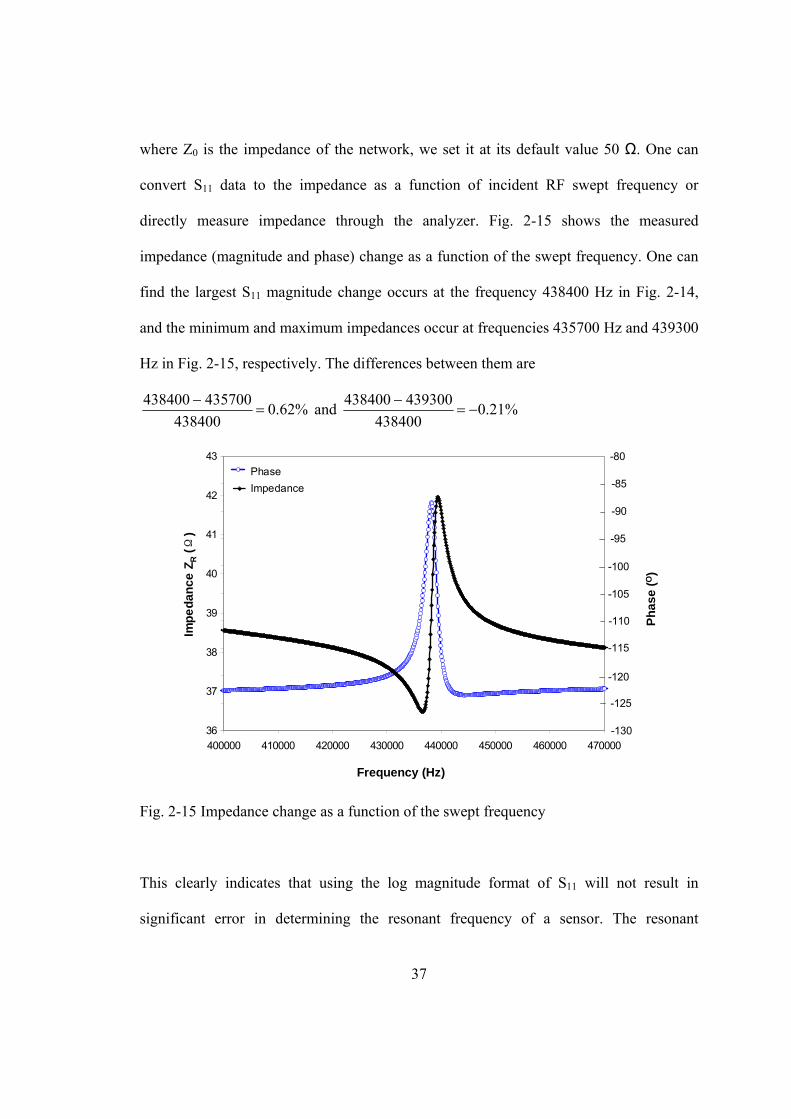
37
where Z0 is the impedance of the network, we set it at its default value 50 Ω. One can
convert S11 data to the impedance as a function of incident RF swept frequency or
directly measure impedance through the analyzer. Fig. 2-15 shows the measured
impedance (magnitude and phase) change as a function of the swept frequency. One can
find the largest S11 magnitude change occurs at the frequency 438400 Hz in Fig. 2-14,
and the minimum and maximum impedances occur at frequencies 435700 Hz and 439300
Hz in Fig. 2-15, respectively. The differences between them are
%62.0438400
435700438400=
− and %21.0438400
439300438400−=
−
Phas
e (O
)
-130
-125
-120
-115
-110
-105
-100
-95
-90
-85
-80
400000 410000 420000 430000 440000 450000 460000 470000
conversion (Z ref.1) on, Phase-80
-85
-90
-95
-100
-105
-110
-115
-120
-125
-13036
37
38
39
40
41
42
43
coversion (Z Ref1.) on, log Mag
Frequency (Hz)
Impe
danc
e Z R
(Ω)
PhaseImpedance
Fig. 2-15 Impedance change as a function of the swept frequency
This clearly indicates that using the log magnitude format of S11 will not result in
significant error in determining the resonant frequency of a sensor. The resonant

38
frequency of the magnetostrictive sensor is therefore determined where the smallest S11
signal magnitude (largest amplitude change) occurs through this study.
39
3. FUNDAMENTALS AND ADVANTAGES OF A SENSOR VIBRATING IN THE
LONGITUDINAL MODE
Before magnetoelastic sensors were developed for mass detection, researchers often
relied on the cantilever- or bridge-based mass sensors that operated in transverse mode.
In fact, sensors fabricated in the cantilever or bridge structure can be actuated in either
transverse vibration (out of plane) or longitudinal vibration (in plane) modes, depending
on the exciting method applied. Microcantilever sensor operation in the transverse mode
is typically driven by an actuation element, and the response is detected by the sensing
element. Electrostatic, thermomechanic and piezoelectric actuation are common
techniques used for actuation, while optical reflections, piezoelectric and piezoresistive
sensing read-out are common techniques for signal detection. The following reviews the
actuation and detection techniques.
3.1. Comparison of the Fundamentals of Vibrating a Cantilever, Bridge, or Beam
System
3.1.1. The Transverse Mode
3.1.1.1. Actuation Techniques
Electrostatic actuation utilizes an electrostatic force that is generated by a charge
from applying a high voltage (>100v) with very little current. A cantilever beam or
40
diaphragm can be excited to vibrate if an A/C electric field is applied. Thermomechanical
actuation is based on the joule resistive heating effect. When a composite beam is
electrically heated (~5-10 v with small mA current), the thermal stress will cause a larger
extension for the higher CTE material, while the counterpart with a lower CTE
component will extend less. As a result, the beam is bent. This method only works at very
low frequencies due to the time necessary for the heat to radiate/diffuse away.
Piezoelectric actuation, on the other hand, is based on the electromechanical coupling
effect exhibited by certain materials. When voltage is applied across two parallel surfaces,
a piezoelectric material will undergo mechanical distortion, i. e. a change in shape, and
vice/versa if mechanical deformation is applied. This method currently drives the
majority of applications needing a resonator or transducer. An earphone, for example,
uses an electrical input to generate a mechanical output. As mentioned above,
piezoelectric materials also exhibit the effect that a voltage drop can be produced when
they are subjected to applied mechanical stress, which has been employed in strain
gauges, microphones, microbalances, and others. Ferrari et al. [35] reported in 1996,
employing the piezoelectric effect to both actuate and sense cantilever resonance and
changed thereof. The mass sensitivity is the range of 280 to 1200 Hz/mg for this type of
mass sensor.
3.1.1.2. Sensing Techniques
Optical reflection, piezoresistance, and electrostatic measurement methods are
commonly used to detect cantilever bending in the static mode [36-44]. Optical
reflection of a focused laser beam on a cantilever can be detected either by a position
41
sensitive detector [44] or by interference of a reference laser beam with the one reflected
by the cantilever [45]. The electrostatic method involves monitoring the capacitance
change due to a bending cantilever or bridge. Optical reflection and piezoresistance are
commonly used for detecting the resonate frequency in the dynamic mode [46, 47].
Pinnaduwage and coworkers [43] reported that the bending signal is much clearer and
easier to measure than the resonant frequency signal. However, when it is operated in a
liquid, especially in an opaque liquid, the laser undergoes refraction in the liquid and
significantly loses intensity in both bending and dynamic modes. In such cases electronic
measurements are more prudent; however, if the cantilever bending is less than 50 nm,
the signal may not be detected by the piezoresistive elements [48] and the large damping
effects of liquid environments may limit the application of the piezoresistive technique.
The magnetostrictive effects to drive and sense cantilever sensors [25, 49-51] in the
transverse mode have been widely studied as well.
3.1.2. The Longitudinal Mode
Longitudinal vibration, the counterpart of the transverse mode, involves resonance
along the structure’s longest axis (in plane vibration). In the past, there were no actuation
techniques available to excite a cantilever or bridge into longitudinal vibration. However,
magnetostrictive materials offer great promise in this mode of actuation. In this method,
magnetic domains respond and switch in the direction of an applied field. This
phenomenon is exhibited in all ferromagnetic materials and will be very useful as a
means to drive a sensor platform in the longitudinal mode (under an externally modulated
magnetic field). The details of the fundamental mechanism and inducing resonance by
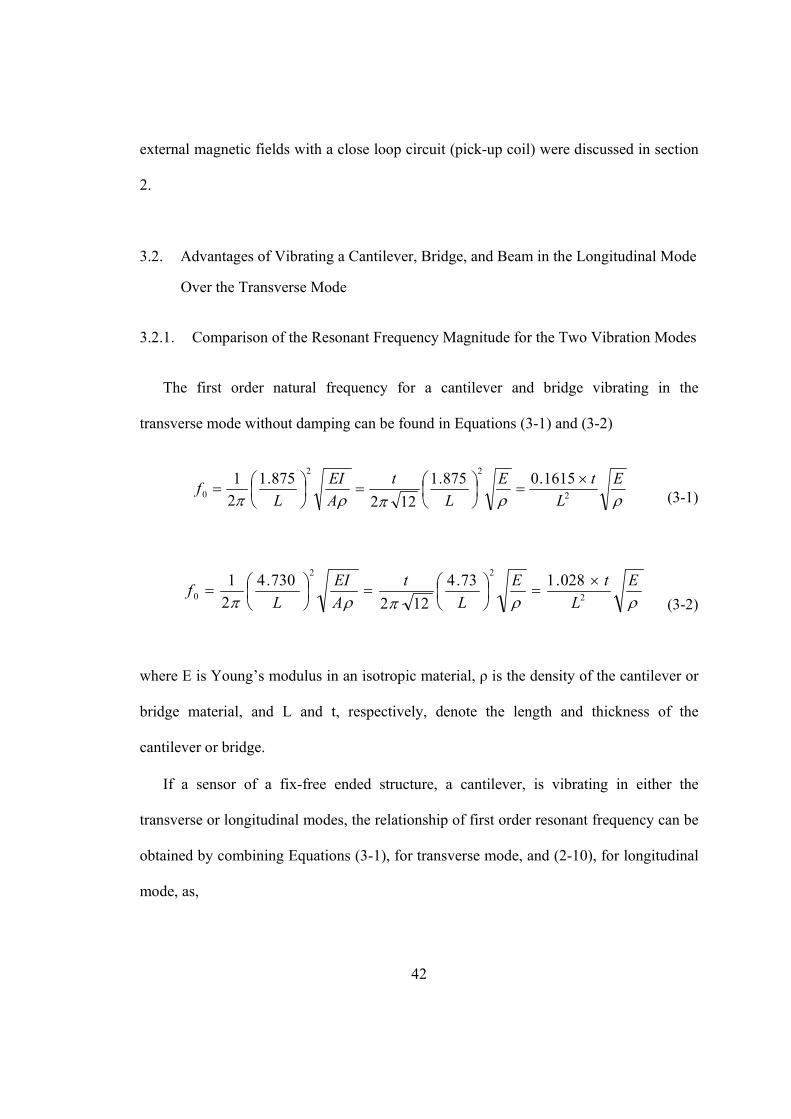
42
external magnetic fields with a close loop circuit (pick-up coil) were discussed in section
2.
3.2. Advantages of Vibrating a Cantilever, Bridge, and Beam in the Longitudinal Mode
Over the Transverse Mode
3.2.1. Comparison of the Resonant Frequency Magnitude for the Two Vibration Modes
The first order natural frequency for a cantilever and bridge vibrating in the
transverse mode without damping can be found in Equations (3-1) and (3-2)
(3-1)
(3-2)
where E is Young’s modulus in an isotropic material, ρ is the density of the cantilever or
bridge material, and L and t, respectively, denote the length and thickness of the
cantilever or bridge.
If a sensor of a fix-free ended structure, a cantilever, is vibrating in either the
transverse or longitudinal modes, the relationship of first order resonant frequency can be
obtained by combining Equations (3-1), for transverse mode, and (2-10), for longitudinal
mode, as,
ρρπρπE
LtE
Lt
AEI
Lf 2
22
01615.0875.1
122875.1
21 ×
=⎟⎠⎞
⎜⎝⎛=⎟
⎠⎞
⎜⎝⎛=
ρρπρπE
LtE
Lt
AEI
Lf 2
22
0028.173.4
122730.4
21 ×
=⎟⎠⎞
⎜⎝⎛=⎟
⎠⎞
⎜⎝⎛=
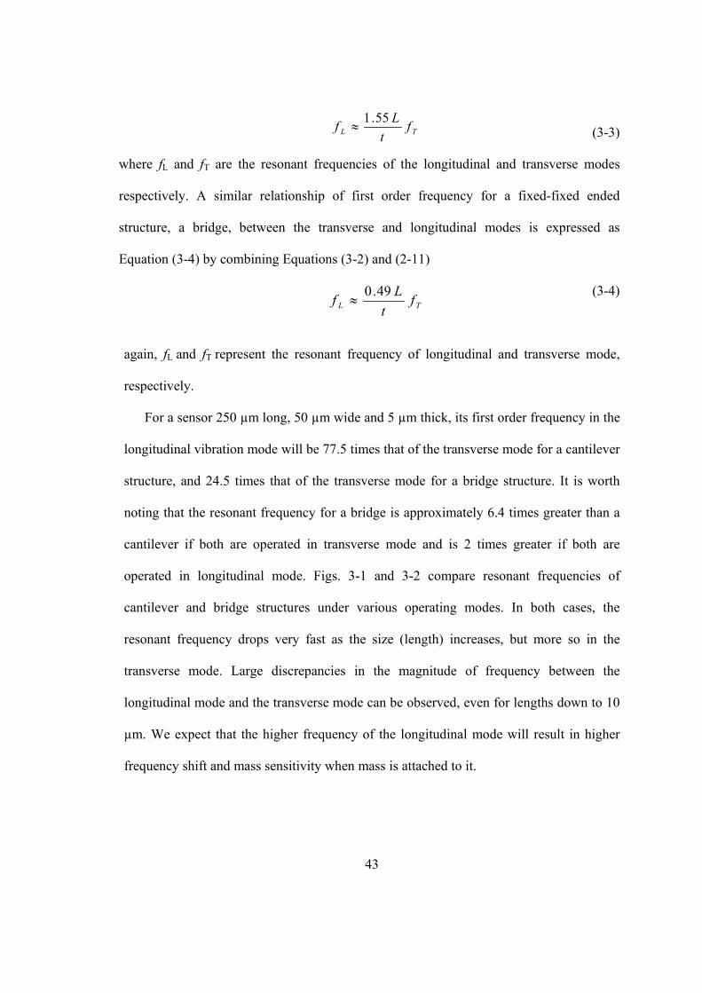
43
(3-3)
where fL and fT are the resonant frequencies of the longitudinal and transverse modes
respectively. A similar relationship of first order frequency for a fixed-fixed ended
structure, a bridge, between the transverse and longitudinal modes is expressed as
Equation (3-4) by combining Equations (3-2) and (2-11)
(3-4)
again, fL and fT represent the resonant frequency of longitudinal and transverse mode,
respectively.
For a sensor 250 µm long, 50 µm wide and 5 µm thick, its first order frequency in the
longitudinal vibration mode will be 77.5 times that of the transverse mode for a cantilever
structure, and 24.5 times that of the transverse mode for a bridge structure. It is worth
noting that the resonant frequency for a bridge is approximately 6.4 times greater than a
cantilever if both are operated in transverse mode and is 2 times greater if both are
operated in longitudinal mode. Figs. 3-1 and 3-2 compare resonant frequencies of
cantilever and bridge structures under various operating modes. In both cases, the
resonant frequency drops very fast as the size (length) increases, but more so in the
transverse mode. Large discrepancies in the magnitude of frequency between the
longitudinal mode and the transverse mode can be observed, even for lengths down to 10
µm. We expect that the higher frequency of the longitudinal mode will result in higher
frequency shift and mass sensitivity when mass is attached to it.
TL ft
Lf 55.1≈
TL ft
Lf 49.0≈
44
0 100 200 300 400 500 600 700 800 900 10006789
1011121314151617181920
length (um)
log(
f)
transverse modelongitudinal mode
Cantilever length (µm)
Freq
uenc
y in
log
scal
e (H
z) t=1µm
Fig. 3-1 Comparison of cantilever resonant frequency operated in different modes.
0 100 200 300 400 500 600 700 800 900 100089
10111213141516171819202122
length(um)
log(
f)
transverse modelongitudinal mode
Bridge length (µm)
Freq
uenc
y in
log
scal
e (H
z) t=1µm
Fig. 3-2 Comparison of bridge resonant frequency operated in different modes.
45
3.2.2. Comparison of Sensitivity for Two Vibration Modes
A mass sensor working in either of the vibration modes will have a sensitivity
expression in the same manner as stated by Equation (2-22), which is
(3-5)
Assuming the sensor has an aspect length to width ratio of at least 5, then the
sensitivity for a cantilever working in transverse mode (SCT) and longitudinal mode (SCL)
is expressed as
(3-6)
Obviously, a cantilever in the longitudinal vibration mode has a much higher sensitivity
than that in the transverse mode, e.g. for a 250 µm x 50 µm x 5 µm cantilever, ρ = 7.9
g/cc. SCT ≈1.28% SCL. This is also true for a bridge with the same size LBBT SS %11.4≈ ,
where SBT and SBL are the sensitivities of bridge operated in the transverse mode and
longitudinal mode, respectively. The relationship of the sensor’s sensitivity for the
transverse mode and the longitudinal mode can be derived and expressed in Equations (3-
7) and (3-8) for cantilever and bridge, respectively.
(3-7)
4
40375.0L
S CT ρυ
≈
tLS CL 3
625.0ρ
υ=
LT SLtS ⎟⎠⎞
⎜⎝⎛≈ 641.0
senmf
mfS
20=
∆∆
=
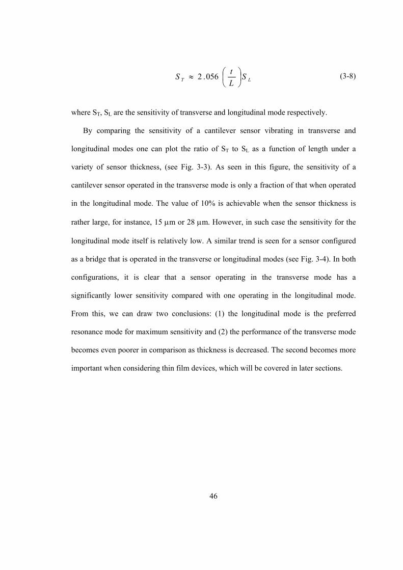
46
(3-8)
where ST, SL are the sensitivity of transverse and longitudinal mode respectively.
By comparing the sensitivity of a cantilever sensor vibrating in transverse and
longitudinal modes one can plot the ratio of ST to SL as a function of length under a
variety of sensor thickness, (see Fig. 3-3). As seen in this figure, the sensitivity of a
cantilever sensor operated in the transverse mode is only a fraction of that when operated
in the longitudinal mode. The value of 10% is achievable when the sensor thickness is
rather large, for instance, 15 µm or 28 µm. However, in such case the sensitivity for the
longitudinal mode itself is relatively low. A similar trend is seen for a sensor configured
as a bridge that is operated in the transverse or longitudinal modes (see Fig. 3-4). In both
configurations, it is clear that a sensor operating in the transverse mode has a
significantly lower sensitivity compared with one operating in the longitudinal mode.
From this, we can draw two conclusions: (1) the longitudinal mode is the preferred
resonance mode for maximum sensitivity and (2) the performance of the transverse mode
becomes even poorer in comparison as thickness is decreased. The second becomes more
important when considering thin film devices, which will be covered in later sections.
LT SLtS ⎟⎠⎞
⎜⎝⎛≈ 056.2
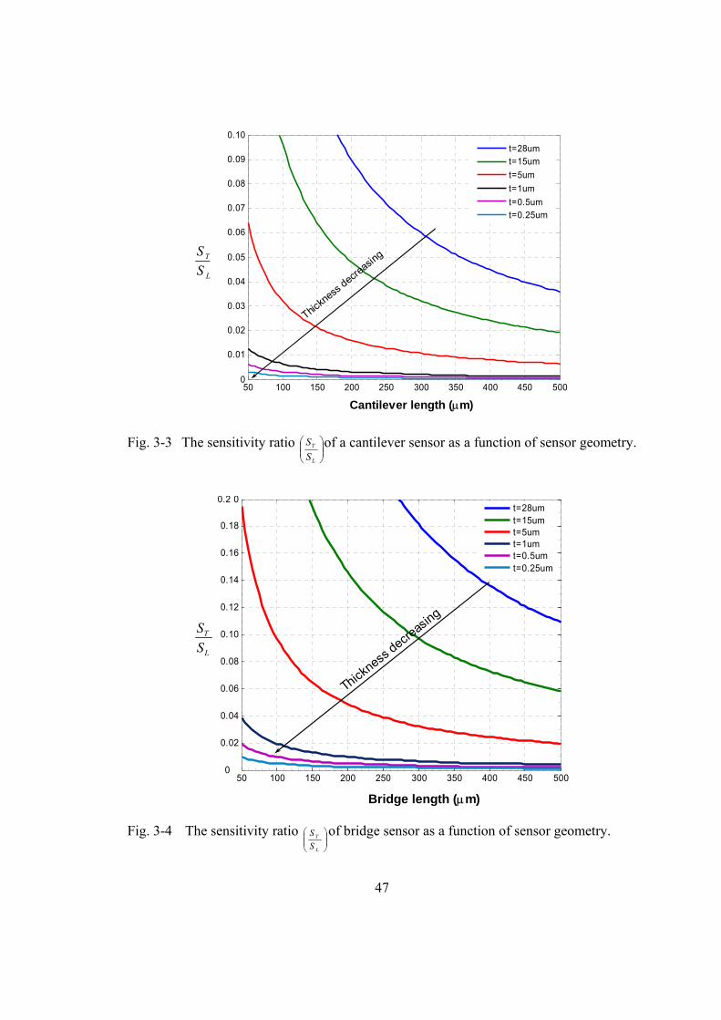
47
50 100 150 200 250 300 350 400 450 5000
0.01
0.02
0.03
0.04
0.05
0.06
0.07
0.08
0.09
0.10
St/S
l
Cantilever length (um)
t=28umt=15umt=5umt=1umt=0.5umt=0.25um
L
T
SS
Thickness
decreasin
g
Cantilever length (µm)
Fig. 3-3 The sensitivity ratio ⎟⎟⎠
⎞⎜⎜⎝
⎛
L
T
SS of a cantilever sensor as a function of sensor geometry.
L
T
SS
Bridge length (µm)
50 100 150 200 250 300 350 400 450 5000
0.02
0.04
0.06
0.08
0.10
0.12
0.14
0.16
0.18
0.2 0t=28umt=15umt=5umt=1umt=0.5umt=0.25um
Thickness
decreasi
ng
Fig. 3-4 The sensitivity ratio ⎟⎟⎠
⎞⎜⎜⎝
⎛
L
T
SS of bridge sensor as a function of sensor geometry.
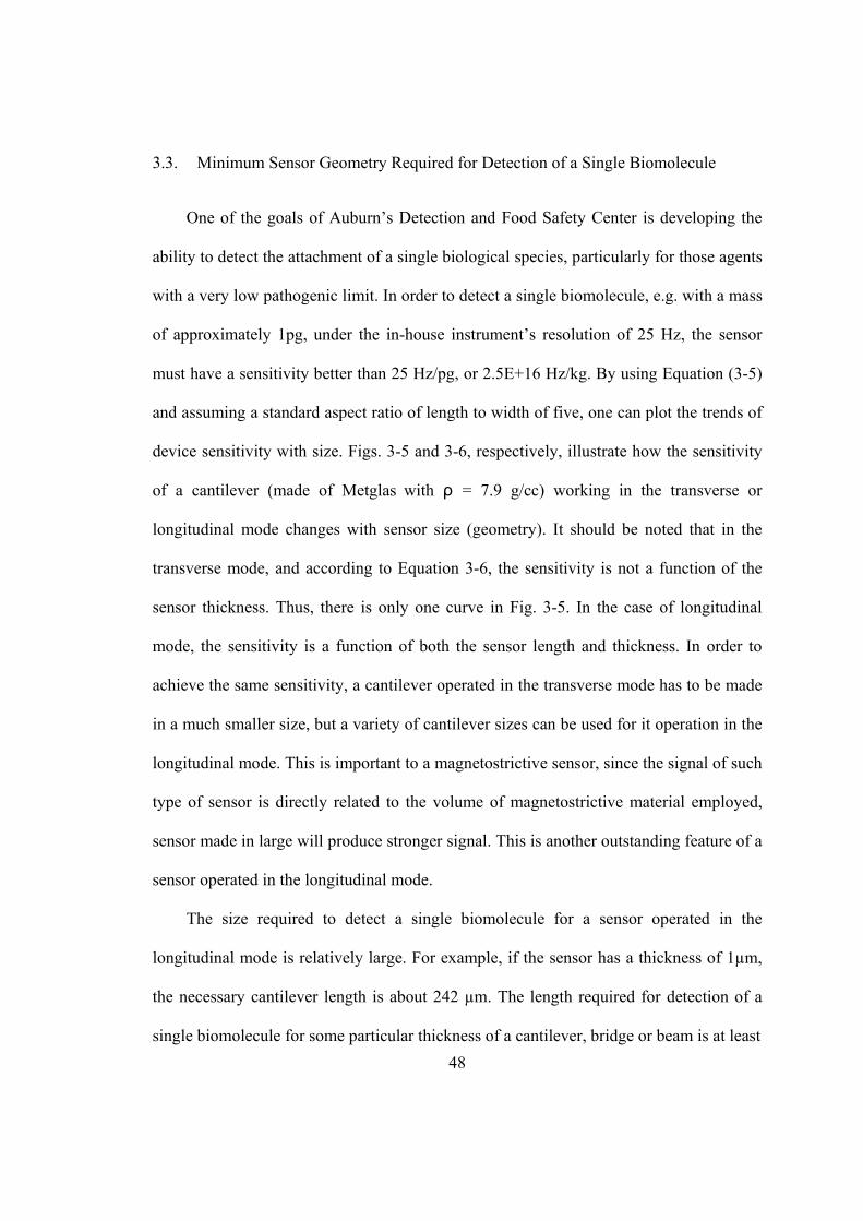
48
3.3. Minimum Sensor Geometry Required for Detection of a Single Biomolecule
One of the goals of Auburn’s Detection and Food Safety Center is developing the
ability to detect the attachment of a single biological species, particularly for those agents
with a very low pathogenic limit. In order to detect a single biomolecule, e.g. with a mass
of approximately 1pg, under the in-house instrument’s resolution of 25 Hz, the sensor
must have a sensitivity better than 25 Hz/pg, or 2.5E+16 Hz/kg. By using Equation (3-5)
and assuming a standard aspect ratio of length to width of five, one can plot the trends of
device sensitivity with size. Figs. 3-5 and 3-6, respectively, illustrate how the sensitivity
of a cantilever (made of Metglas with ρ = 7.9 g/cc) working in the transverse or
longitudinal mode changes with sensor size (geometry). It should be noted that in the
transverse mode, and according to Equation 3-6, the sensitivity is not a function of the
sensor thickness. Thus, there is only one curve in Fig. 3-5. In the case of longitudinal
mode, the sensitivity is a function of both the sensor length and thickness. In order to
achieve the same sensitivity, a cantilever operated in the transverse mode has to be made
in a much smaller size, but a variety of cantilever sizes can be used for it operation in the
longitudinal mode. This is important to a magnetostrictive sensor, since the signal of such
type of sensor is directly related to the volume of magnetostrictive material employed,
sensor made in large will produce stronger signal. This is another outstanding feature of a
sensor operated in the longitudinal mode.
The size required to detect a single biomolecule for a sensor operated in the
longitudinal mode is relatively large. For example, if the sensor has a thickness of 1µm,
the necessary cantilever length is about 242 µm. The length required for detection of a
single biomolecule for some particular thickness of a cantilever, bridge or beam is at least
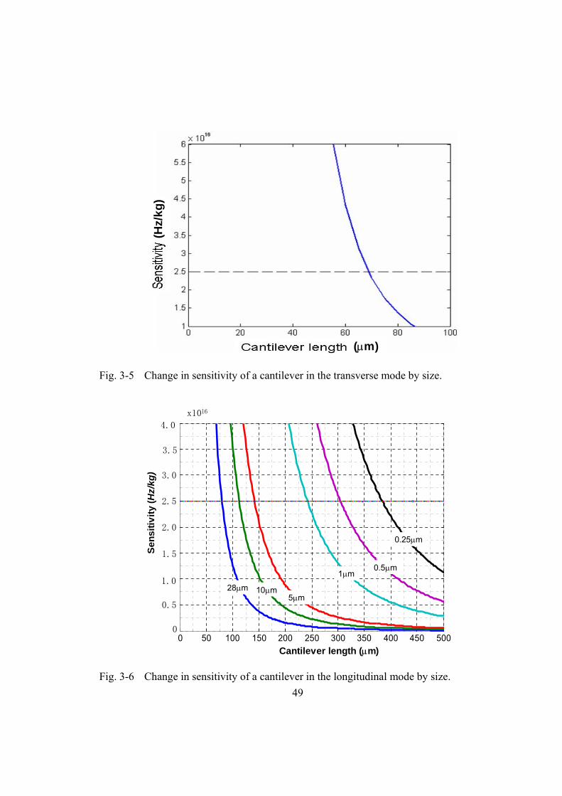
49
(µm)
(Hz/
kg)
Fig. 3-5 Change in sensitivity of a cantilever in the transverse mode by size.
0 50 100 150 200 250 300 350 400 450 500Cantilever length (µm)
Sens
itivi
ty (H
z/kg
)
0
0.5
1.0
1.5
2.0
2.5
3.0
3.5
4.0
x1016
28µm 10µm5µm
1µm0.5µm
0.25µm
Cantilever length (µm)
Fig. 3-6 Change in sensitivity of a cantilever in the longitudinal mode by size.
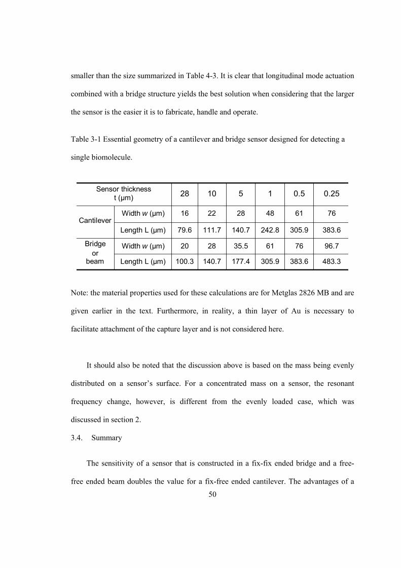
50
smaller than the size summarized in Table 4-3. It is clear that longitudinal mode actuation
combined with a bridge structure yields the best solution when considering that the larger
the sensor is the easier it is to fabricate, handle and operate.
Table 3-1 Essential geometry of a cantilever and bridge sensor designed for detecting a
single biomolecule.
Length L (µm)
Width w (µm)
483.3383.6305.9177.4140.7100.3
Length L (µm)
Width w (µm)
383.6305.9242.8140.7111.779.6
96.7766135.52820Bridge or
beam
766148282216Cantilever
0.250.5151028Sensor thickness t (µm)
Note: the material properties used for these calculations are for Metglas 2826 MB and are
given earlier in the text. Furthermore, in reality, a thin layer of Au is necessary to
facilitate attachment of the capture layer and is not considered here.
It should also be noted that the discussion above is based on the mass being evenly
distributed on a sensor’s surface. For a concentrated mass on a sensor, the resonant
frequency change, however, is different from the evenly loaded case, which was
discussed in section 2.
3.4. Summary
The sensitivity of a sensor that is constructed in a fix-fix ended bridge and a free-
free ended beam doubles the value for a fix-free ended cantilever. The advantages of a
51
mass sensor operated in the longitudinal mode as opposed to the conventional transverse
mode were discussed by a comprehensive comparison of frequency and mass sensitivity
for cantilever and bridge operation in both the transverse and longitudinal modes. The
mass sensitivity of a sensor operated in the transverse was found to possess only a
fraction of the sensitivity when operated in the longitudinal mode.
The fundamental size requirement of a miniaturized sensor, it is fabricated in the
structure of cantilever or bridge, and operated in both vibrating modes was addressed, so
that sensors can be optimized to detect mass attachments on the order of a single spore or
cell. It was found that a cantilever sensor operated in the transverse mode must be
designed as small as 70 µm in length so that it is possible to detect a single spore, while a
cantilever sensor operated in the longitudinal mode can detect the same mass at a
significantly larger sensor size. This is important for easier fabrication, operation and
handling of the sensors.
52
4. CORRECTION TO THIN, SLENDER BEAM VIBRATING IN THE
LONGITUDINAL MODE PRINCIPLE AND VALIDATION OF PROOF-OF-
CONCEPT EQUATIONS
The potential applications of a resonated sensor for measuring thin film Young’s
modulus and mass detection have been discussed in the preceding sections. To better
understand the mechanism of a sensor operated in the longitudinal vibration mode finite
element analysis was employed to numerically simulate the magnetostrictive sensors.
This section reports on these results and details the modification and verification of the
operation principle of a thin slender beam vibrating in the longitudinal mode. In addition
to the finite element analysis, proof-of-principle for this modification was also verified by
experimentation. Metglas 2826 MB and its material properties were used as the sensor
material for both experimentation and simulation.
4.1. Introduction
Mass sensors based on a cantilever operating in the transverse mode have received
extensive research interest over the past decade or so due to the ease and convenience of
actuating and measuring resonance behavior. However, as demonstrated in the previous
section, the sensitivity of this type of sensor is rather low in comparison to other
vibrational modes for the identical structure. In recent years, magnetostrictive materials
have enabled the longitudinal vibration mode to be considered as the resonance mode of a
sensor platform. Unfortunately, most of the attention in this area has only been focused
on the relationship between the relative resonant frequency shift and the relative mass
53
change of the sensor, which is prudent, but only in cases where mass is the only
parameter influencing the resonant frequency change. To the best of the author’s
knowledge, little effort has been focused on addressing the fundamental aspects of
cantilever/bridge operation in the longitudinal. For example, the geometry causes other
parameters to influence behavior. It is important to have a clearer understanding of these
issues so that device design may be improved and optimized.
The first step in the numerical simulations was the assumption that the cross-section
of the bar remains in-plane during longitudinal vibration. In reality, when a slender bar,
such as a cantilever, bridge or freestanding beam, vibrates in the longitudinal mode, the
lateral strain induced by the longitudinal stress is small and negligible since the
longitudinal wave is much larger in comparison to the cross-sectional dimensions of the
bar. In such case, the first order resonant frequency can be obtained by
ρE
Lf
41
=
and
ρE
Lf
21
=
for a cantilever and bridge/freestanding beam respectively [28, 30, 52], as discussed in
section 2. These equations are the general reflections of bars configured in their
respective structures. These equations hold for general dimensions where length, width
and thickness are comparable in magnitude. However, as one or more dimensions
become significantly different in magnitude, say a sufficient reduction in size,
geometrical effects begin to play a role in the form of the Poisson Effect, whereby the
reduced dimensions cause a different response to straining governed by the materials
54
dimensions and Poisson’s ratio. In the case of Metglas tape with a thickness of 28µm, the
dimensions are on the order of L>w>>t. This defines a plate-like situation where
cantilever, bridge or beam structures subjected to the elastic deformation in the
longitudinal direction will be under a state of plane-stress rather than uniaxial-stress. As
such, Poisson’s ratio would play a different role in resonance behavior. In general,
Landau [30] suggested replacing Young’s modulus E with the plane-strain modulus E/(1-
ν2) for deformation of plate-like structures. Harris [52] and Timoshenko [28], however
believed the above equations still hold true for the plate case. These arguments are
contradictory to some extent, but the extensive experimental work with cantilevers in the
transverse mode has demonstrated that geometry influences which modulus to use, i.e.
the plane-strain, plane-stress or uniaxial modulus. This issue has yet to be studied and the
early work in applying Metglas strips in longitudinal mode resonance employed the
plane-strain modulus in accordance with Landau [14, 53, 54]. However, when one
experimentally measures the resonant frequency of a cantilever or beam in longitudinal
vibration, the measured values are much higher than the calculated values predicted by
the equations cited above. For example, a freestanding beam with a dimension of 8 mm x
1.6 mm x 28 µm that is made of Metglas with a density of 7.9 g/cc and Young’s modulus
of 105 GPa [10] has a measured resonant frequency of 274,700 Hz in the longitudinal
mode. If we assume Poisson’s ratio of this material is 0.33, which is typical for an
amorphous glassy metal, the calculated frequencies will be 227,856 Hz and 241,378 Hz
by Timoshenko and Landau’s equations, respectively. Either case is lower, whereas real-
life damping effects should cause the measured value to be lower then the calculated one.
55
Equation (4-1) is the widely cited form adopted by many papers [13, 14, 17, 19, 53-57]
that deal with Metglas operated in longitudinal vibration.
(4-1)
For this equation if Poisson’s ratio 0.5 is used, and the results seem to agree. However,
Poisson’s ratio for Metglas was measured to be 0.33 by Chou et al. [58], and should be
the values employed. Additionally, a metal should not posses a Poisson’s ratio 0.5.
Table (4-1) lists the resonant frequencies obtained from different equations and
experimental tests for different geometries vibrated in the longitudinal mode. In the
calculation, Poisson’s ratio 0.33 was used.
Table 4-1 Comparison of resonant frequencies calculated by using E and plane-strain
modulus E/(1-ν2) with experimental test for freestanding beam cantilever and bridge at
different lengths.
ExperimentalPlane StrainE/(1-ν2)
UniaxialE
153.9
123.7
274.7
134.1
107.3
242.7
126.6
101.3
227.9
(kHz)
Bridge
Cantilever
Freestanding
Structure
14.4
9
8
L(mm)
)1(21
2νρ −=
EL
f
56
The discrepancy in the values of the calculated resonant frequencies that are lower
than the measured values must relate to the chosen state of strain in the structure, which
manifests from the three-dimensional combination of elastic extension and contraction
strains. Since the bars are more plate-like they are likely to be in a state of plane-stress. In
such a case, the elastic modulus should be replaced by the plane-stress modulus E/(1-ν).
Given that the effect of the different dimensions on the state of strain are uncertain, it is
possible that for the given dimensions the effect lies between plane-stress and plane-
strain, the difference being the operating power of Poisson’s ratio.
In order to investigate this hypothesis we began by assuming that the importance of
Poisson’s ratio influence is variable and denoted as n. This enables us to investigate the
potential for plane-stress conditions [Eplane-stress = E/(1-v)] [59] or a mixture of plane-
strain and plane-stress conditions. Therefore, the first order longitudinal vibration
frequency for a thin, slender, cantilever can be expressed as Equation (4-2)
(4-2)
Similarly, the first order longitudinal vibration frequency for the fix-fix ended bridge or
free-free ended beam can be expressed by Equation (4-3).
(4-3)
(4-4)
)1(41
n
EL
fνρ −
=
)1(21
n
EL
fνρ −
=
)1( n
Eνρ
υ−
=
57
where ν is Poisson’s ratio, and υ is often referred to as the acoustic wave propagation
speed, which is an intrinsic material property. Both experimentation and simulation were
conducted to assess the state of strain present in the cantilever and bridge structures.
4.2. Determination of the Correct Analytical Solution for Thin Slender Beams
In order to determine the value of n in Equation (4-3) it was important to first
measure the acoustic wave propagation speed experimentally, which can then be plugged
into Equation (4-4) to determine the relationship between Poisson’s ratio and operation
number n. The wave speed measurement was accomplished by measuring the resonant
frequency of thin strips of several different lengths and then plotting frequency vs length,
the signature of which can be fitted with regression to extract the wave speed. This will
enable the exponent n to be expressed in terms of Poisson’s ratio via Equation 4-4. In
turn, numerical simulations employing modal analysis will be performed to determine
resonant frequency as Poisson’s ratio is systematically varied and consequently yield
values of n that satisfy Equation 4-3. When the acoustic wave speed of the experiments
and the simulations is equal, the true Poisson’s ratio and the value of its exponent can be
identified.
To investigate these issues several samples of magnetostrictive strips were prepared
and tested in order to determine the wave propagation speed in the medium. Rectangular
strips of commercially obtained Metglas 2826 MB 28 µm thick were cut with a dicing
saw to the sizes and aspect ratios listed in Table 4-2. Followed cutting, all specimens
were cleaned and prepared for testing. The strips were subjected to a modulated external
magnetic field in order to drive them to resonance while their time-dependent response
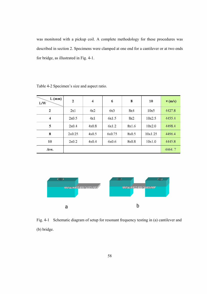
58
was monitored with a pickup coil. A complete methodology for these procedures was
described in section 2. Specimens were clamped at one end for a cantilever or at two ends
for bridge, as illustrated in Fig. 4-1.
Table 4-2 Specimen’s size and aspect ratio.
a b
Fig. 4-1 Schematic diagram of setup for resonant frequency testing in (a) cantilever and
(b) bridge.
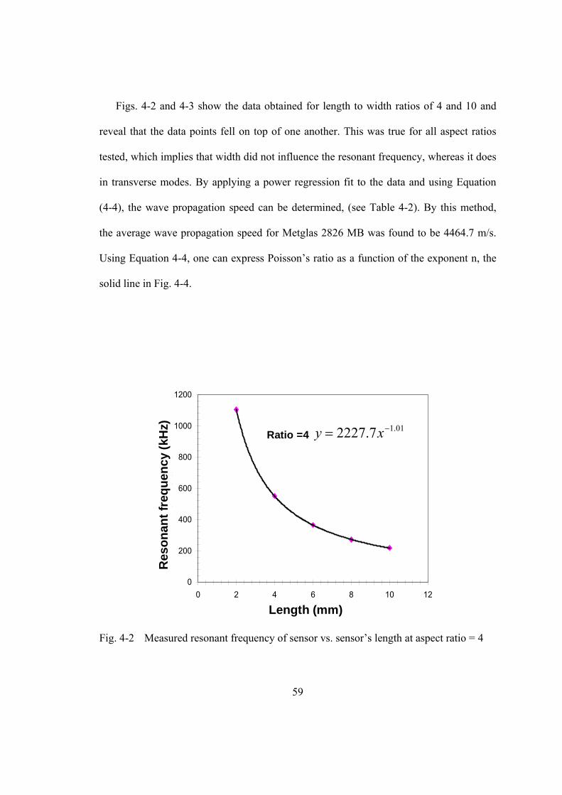
59
Figs. 4-2 and 4-3 show the data obtained for length to width ratios of 4 and 10 and
reveal that the data points fell on top of one another. This was true for all aspect ratios
tested, which implies that width did not influence the resonant frequency, whereas it does
in transverse modes. By applying a power regression fit to the data and using Equation
(4-4), the wave propagation speed can be determined, (see Table 4-2). By this method,
the average wave propagation speed for Metglas 2826 MB was found to be 4464.7 m/s.
Using Equation 4-4, one can express Poisson’s ratio as a function of the exponent n, the
solid line in Fig. 4-4.
ratio=4 y = 2227.7x-1.01
0
200
400
600
800
1000
1200
0 2 4 6 8 10 12
length (mm)
freq
uenc
y (K
Hz)
Length (mm)
Res
onan
t fre
quen
cy (k
Hz)
Ratio =401.17.2227 −= xy
Fig. 4-2 Measured resonant frequency of sensor vs. sensor’s length at aspect ratio = 4
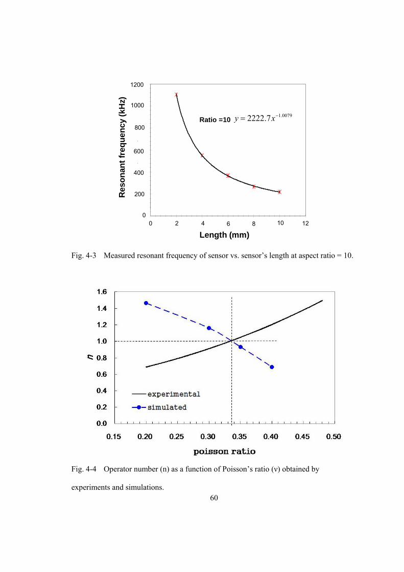
60
Ratio =10 0079.17.2222 −= xyratio=10 y = 2222.7x-1.0079
0
200
400
600
800
1000
1200
0 2 4 6 8 10 12
length(mm)
freq
uenc
y (K
Hz)
Length (mm)
Res
onan
t fre
quen
cy(k
Hz)
Ratio =10 0079.17.2222 −= xy
0 2 4 6 8 10 1200
200
400
600
800
1000
1200
Res
onan
t fre
quen
cy (k
Hz)
Length (mm)
Fig. 4-3 Measured resonant frequency of sensor vs. sensor’s length at aspect ratio = 10.
Fig. 4-4 Operator number (n) as a function of Poisson’s ratio (ν) obtained by
experiments and simulations.
61
In order to pinpoint Poisson’s ratio for Metglas 2826 MB and the corresponding state
of strain, finite element simulations were carried out using commercially available
software from CoventorWare [60]. Specifically, the simulations involved modal analysis
on an undamped, free-free slender bar with oscillations in the longitudinal mode. A
magnetostrictive sensor with 8 mm x 1.6 mm x 28 µm size was used for simulation. The
selected mesh type was Manhattan brick, the element order was set to parabolic, and
element size was 160 x 160 x 5.6 µm3, see Fig. 4-5. The material properties employed in
the simulations were identical to those in the experimental analysis above. Poisson’s ratio
was systematically varied and the corresponding influence on resonant frequency was
recorded as listed in Table 4-3 . One can then plug this information into Equation 4-3 to
obtain Poisson’s ratio exponent n, (see Table 4-3). These results essentially identify how
the acoustic wave velocity is influenced by Poisson’s ratio. When comparing them with
the experimental results, consensus should be reached when the acoustic wave velocities
match. Fig. 4-4 shows the overlie of the experimental data and simulation results, dashed
line with circles, that reveals the velocities match at a Poisson’s ratio of 0.33. This agrees
with values tested by the supplier and published in 1979 [58]. Moreover, this corresponds
to Poisson’s ratio exponent of one clarifying that plane-stress/biaxial-modulus conditions
dominate behavior for the geometry and dimensions used. Thus, the natural frequency
relationship for a freestanding strip, bridge or cantilever should be modified using the
plane-stress or biaxial modulus per Equation (4-5) for a cantilever and (4-6) for a bridge
or freestanding beam,
(4-5) )1(412
νρ −−
=E
Lnf
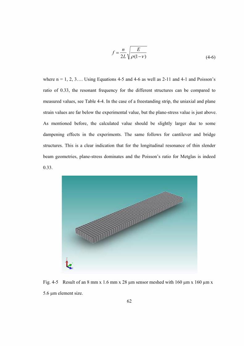
62
(4-6)
where n = 1, 2, 3…. Using Equations 4-5 and 4-6 as well as 2-11 and 4-1 and Poisson’s
ratio of 0.33, the resonant frequency for the different structures can be compared to
measured values, see Table 4-4. In the case of a freestanding strip, the uniaxial and plane
strain values are far below the experimental value, but the plane-stress value is just above.
As mentioned before, the calculated value should be slightly larger due to some
dampening effects in the experiments. The same follows for cantilever and bridge
structures. This is a clear indication that for the longitudinal resonance of thin slender
beam geometries, plane-stress dominates and the Poisson’s ratio for Metglas is indeed
0.33.
Fig. 4-5 Result of an 8 mm x 1.6 mm x 28 µm sensor meshed with 160 µm x 160 µm x
5.6 µm element size.
)1(2 νρ −=
ELnf
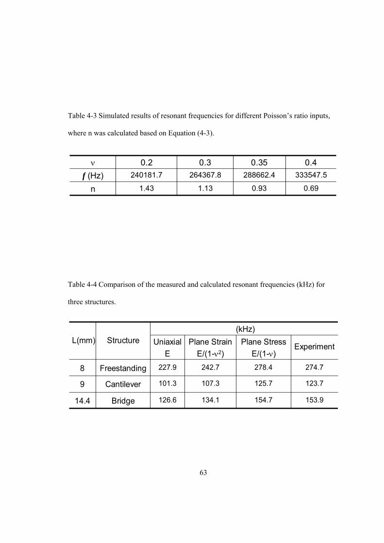
63
Table 4-3 Simulated results of resonant frequencies for different Poisson’s ratio inputs,
where n was calculated based on Equation (4-3).
0.69
333547.50.4
0.93
288662.40.35
1.13
264367.80.3
1.43
240181.70.2
nf (Hz)ν
Table 4-4 Comparison of the measured and calculated resonant frequencies (kHz) for
three structures.
154.7
125.7
278.4
Plane StressE/(1-ν)
ExperimentPlane StrainE/(1-ν2)
UniaxialE
153.9
123.7
274.7
134.1
107.3
242.7
126.6
101.3
227.9
(kHz)
Bridge
Cantilever
Freestanding
Structure
14.4
9
8
L(mm)
64
4.3. Experimental Test and Numerical Analysis to Verify the Longitudinal Mode
Proof-of-Principle
4.3.1. Experimental verification of the Proof-of-Principle Equations
In order to verify that the mode equations given above are appropriate, additional
experimental and numerical analysis will be performed using the first and second
resonate state of the cantilever and bridge structures. The corrected resonant frequency
relationships were stated in Equations (4-5) and (4-6). A series of experimental tests were
carried out in the fashion of cantilever, bridge and cantilever array. The first two resonant
states of a 14.4 mm long cantilever were recorded and are shown in Fig. 4-6. The second
state was approximately three times that of the first state, and on examining Equation 4-5
the 2n-1 portion becomes 2 x 2 - 1 = 3, which confirms that the frequency magnitude of
the second mode is 3 times that of the first mode. Fig. 4-7 is the resonant frequency
record for a fixed-fixed ended bridge 14.4 mm long. The second mode is approximately 2
times the first mode which is verified with Equation 4-6 where n = 2. Thus, the analytical
solutions in Equations 4-5 and 4-6 are correct.
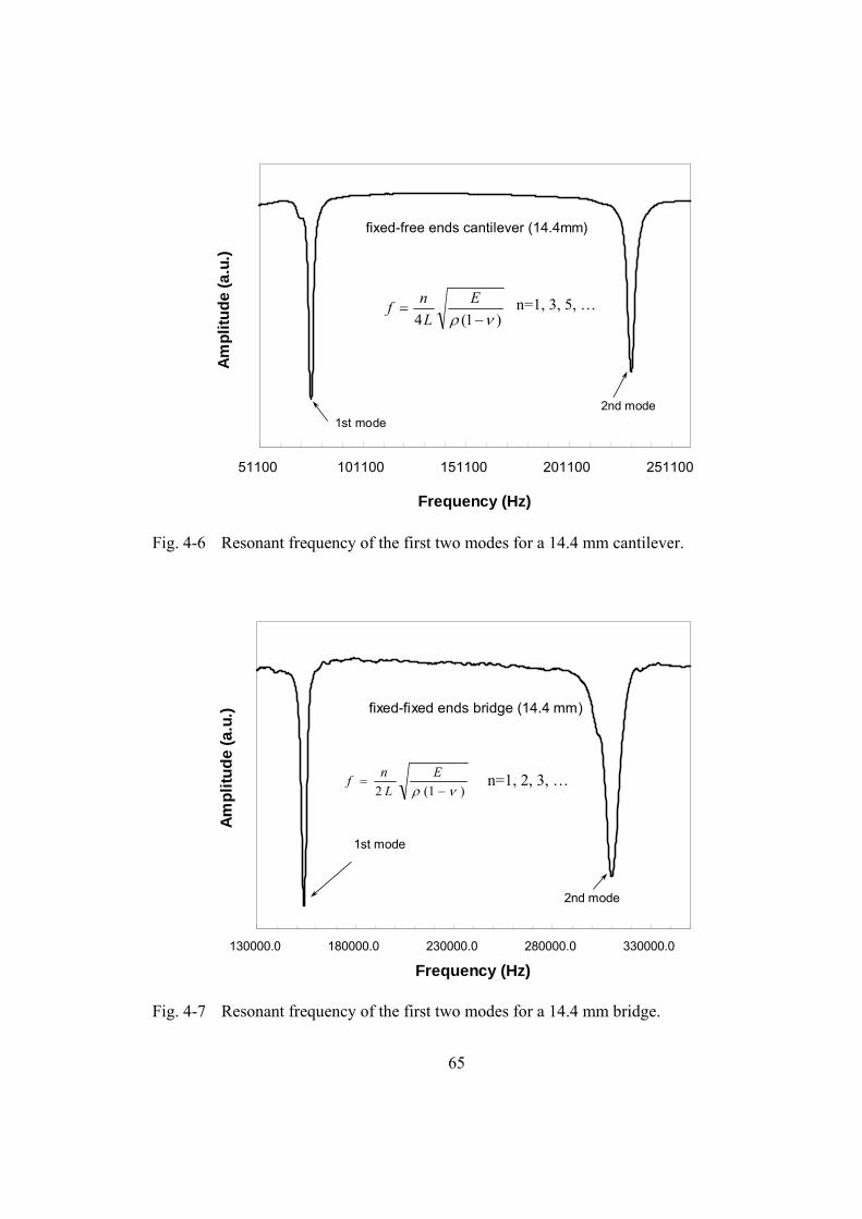
65
)1(4 νρ −=
EL
nf n=1, 3, 5, …
51100 101100 151100 201100 251100
Frequency (Hz )
Ampl
itude
(A.U
.)fixed-free ends cantilever (14.4mm)
76 kHz 1st mode231.4 kHz 2nd mode
1st mode
Ampl
itude
(a.u
.)
Frequency (Hz)
Fig. 4-6 Resonant frequency of the first two modes for a 14.4 mm cantilever.
fixed-fixed ends beam (14.4 mm)
130000.0 180000.0 230000.0 280000.0 330000.0Frequency (Hz )
Am
plitu
de (A
.U.)
1st mode
2nd mode
)1(2 νρ −=
EL
nf n=1, 2, 3, …
fixed-fixed ends bridge (14.4 mm)
Ampl
itude
(a.u
.)
Frequency (Hz)
Fig. 4-7 Resonant frequency of the first two modes for a 14.4 mm bridge.
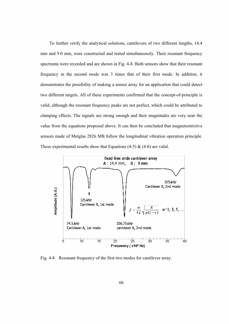
66
To further verify the analytical solutions, cantilevers of two different lengths, 14.4
mm and 9.0 mm, were constructed and tested simultaneously. Their resonant frequency
spectrums were recorded and are shown in Fig. 4-8. Both sensors show that their resonant
frequency in the second mode was 3 times that of their first mode. In addition, it
demonstrates the possibility of making a sensor array for an application that could detect
two different targets. All of these experiments confirmed that the concept-of-principle is
valid, although the resonant frequency peaks are not perfect, which could be attributed to
clamping effects. The signals are strong enough and their magnitudes are very near the
value from the equations proposed above. It can then be concluded that magnetostrictive
sensors made of Metglas 2826 MB follow the longitudinal vibration operation principle.
These experimental results show that Equations (4-5) & (4-6) are valid.
Fig. 4-8 Resonant frequency of the first two modes for cantilever array.
67
4.3.2. Numerical verification of the Proof-of-Principle Equations
Numerical analysis was also applied to the proof-of-principle to provide a final
verification. A series of experiments by simulation were conducted to confirm the
validity of Equations (4-5) and (4-6) for cantilever, bridge and beam. Table 4-5 lists the
results of a cantilever of 80 µm x 20 µm x 1.0 µm. One can see the relationship of
resonant frequency between the higher order mode and the first order mode is 1, 3, 5, 7
and so on. Fig. 4-9 shows the sensors’ shapes under a different order of modes. Tables 4-
6 and 4-7 summarize the simulation results of a bridge made of Metglas with 14.4 mm x
3.0 mm x 28 µm and a beam made of Au with 8 mm x 2 mm x 28 µm, respectively. The
same relationship of the resonant frequency between the higher order mode and the first
order mode is 1, 2, 3, and so on regardless of the materials and configurations in bridge or
beam. These simulation results confirmed the validity of the general equations of the
longitudinal vibrating cantilever, bridge and beam proposed before.
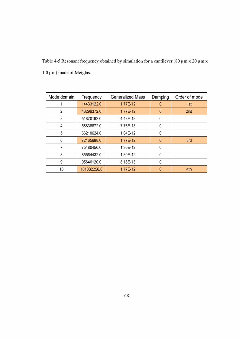
68
Table 4-5 Resonant frequency obtained by simulation for a cantilever (80 µm x 20 µm x
1.0 µm) made of Metglas.
4th01.77E-12101032256.010
08.18E-1395646120.09
01.30E-1285564432.08
01.30E-1275480456.073rd01.77E-1272165688.06
01.04E-1266210624.05
07.76E-1358838872.04
04.43E-1351870192.03
2nd01.77E-1243299372.02
1st 01.77E-1214433122.01Order of modeDampingGeneralized MassFrequencyMode domain
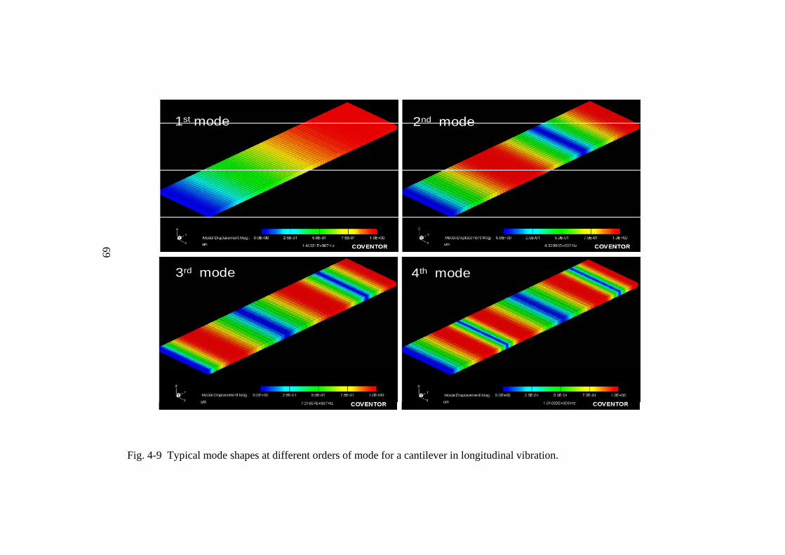
69
Fig. 4-9 Typical mode shapes at different orders of mode for a cantilever in longitudinal vibration.
1st mode 2nd mode
3rd mode 4th mode
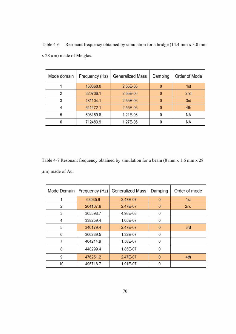
70
Table 4-6 Resonant frequency obtained by simulation for a bridge (14.4 mm x 3.0 mm
x 28 µm) made of Metglas.
NA01.27E-06712483.96
NA01.21E-06698189.85
4th02.55E-06641472.143rd02.55E-06481104.13
2nd02.55E-06320736.12
1st02.55E-06160368.01
Order of ModeDampingGeneralized MassFrequency (Hz)Mode domain
Table 4-7 Resonant frequency obtained by simulation for a beam (8 mm x 1.6 mm x 28
µm) made of Au.
01.91E-07495718.7104th02.47E-07476251.29
01.85E-07448299.48
01.58E-07404214.9701.32E-07366239.56
3rd02.47E-07340179.45
01.05E-07338259.44
04.98E-08305598.73
2nd02.47E-07204107.621st02.47E-0768035.91
Order of modeDampingGeneralized MassFrequency (Hz)Mode Domain
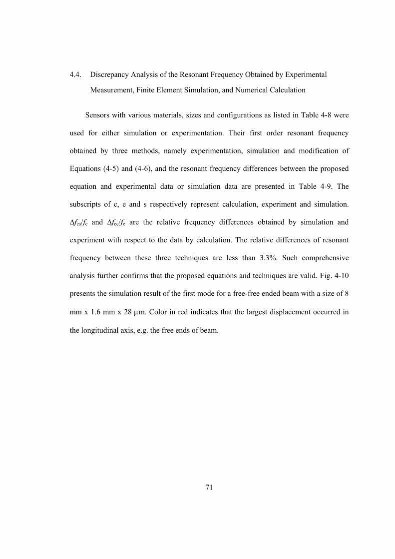
71
4.4. Discrepancy Analysis of the Resonant Frequency Obtained by Experimental
Measurement, Finite Element Simulation, and Numerical Calculation
Sensors with various materials, sizes and configurations as listed in Table 4-8 were
used for either simulation or experimentation. Their first order resonant frequency
obtained by three methods, namely experimentation, simulation and modification of
Equations (4-5) and (4-6), and the resonant frequency differences between the proposed
equation and experimental data or simulation data are presented in Table 4-9. The
subscripts of c, e and s respectively represent calculation, experiment and simulation.
∆fcs/fc and ∆fce/fc are the relative frequency differences obtained by simulation and
experiment with respect to the data by calculation. The relative differences of resonant
frequency between these three techniques are less than 3.3%. Such comprehensive
analysis further confirms that the proposed equations and techniques are valid. Fig. 4-10
presents the simulation result of the first mode for a free-free ended beam with a size of 8
mm x 1.6 mm x 28 µm. Color in red indicates that the largest displacement occurred in
the longitudinal axis, e.g. the free ends of beam.
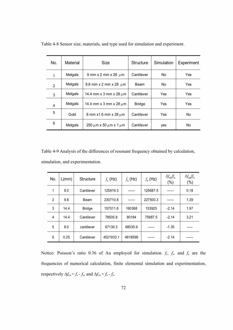
72
Table 4-8 Sensor size, materials, and type used for simulation and experiment.
NoyesCantilever250 µm x 50 µm x 1 µmMetgals6
Gold
Metgals
Metgals
Metgals
Metgals
Material
YesNoCantilever9 mm x 2 mm x 28 µm1
No
Yes
Yes
Yes
Experiment
NoBeam9.8 mm x 2 mm x 28 µm2
YesCantilever14.4 mm x 3 mm x 28 µm3
YesBridge14.4 mm x 3 mm x 28 µm4
YesCantilever8 mm x1.6 mm x 28 µm5
SimulationStructureSizeNo.
Table 4-9 Analysis of the differences of resonant frequency obtained by calculation,
simulation, and experimentation.
-------2.14------46185994521933.1Cantilever0.256
8.0
14.4
14.4
9.8
9.0
L(mm)
0.18------125687.5------125919.3Cantilever1
-----
3.21
1.97
1.39
∆fce/fc
(%)
------227500.3------230710.8Beam2
-2.14153925160368157011.6Bridge3
-2.1475987.58018478505.8Cantilever4
-1.35------68035.967130.3cantilever5
∆fcs/fc(%)
fe (Hz)fs (Hz)fc (Hz)StructureNo.
Notice: Poisson’s ratio 0.36 of Au employed for simulation. fc, fs, and fe are the
frequencies of numerical calculation, finite elemental simulation and experimentation,
respectively ∆fcs = fc - fs, and ∆fce = fc - fe.
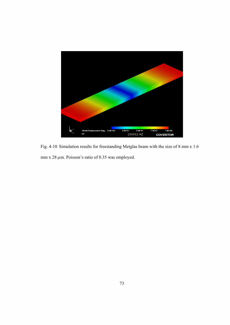
73
Fig. 4-10 Simulation results for freestanding Metglas beam with the size of 8 mm x 1.6
mm x 28 µm. Poisson’s ratio of 0.35 was employed.
74
4.5. Summary
Simulation results have verified that experimental data obtained for magnetostrictive
sensors constructed in cantilevers and bridges was indeed resonating in the longitudinal
mode. In conjunction with simulation and experimental data, theoretical equations for
predicting the resonant frequency of cantilever, bridge and beam were modified by
replacing a plane-strain modulus with a plane-stress modulus (biaxial modulus). The
proof-of-principal equations were validated. Poisson’s ratio of Metglas 2826 MB was
defined to be about 0.33, which is confirmed by the result of earlier study on Metglas and
the supplier’s claimed data.
75
5. BULK-SCALE MAGNETOSTRICTIVE SENSORS
The potential applications of a magnetostrictive sensor vibrated in the longitudinal
mode to measure a thin film elastic modulus and detect mass deposited on the sensor’s
surface have been discussed in the earlier sections. In this section, the details of these
applications will be discussed. Bulk scale, freestanding sensors 8 mm x1.6 mm were
employed to determine the thin film elastic modulus, and 5 mm x 1 mm ones were used
to detect the concentrated mass attached to the sensor’s surface at different locations.
Finite element simulations were employed to confirm the results from the thin film
measurements and mass concentration experiments. In order to confirm the application of
employing magnetostrictive sensors to measure a thin film Young’s modulus, simulation
experiments for freestanding beams with thin films of either Cu or Au were carried out to
verify the experimental results and validate the technique. FEM was also performed to
investigate the potential for Metglas sensors to detect the attachment of a single spore or
cell on the surface and the response for multiple spores or cells attachments.
5.1. Thin Film Elastic Modulus Measurement
Thin film materials such as Al, Au, Cu, etc. have been widely employed in
microelectronic and microelectromechanical systems (MEMS) as interconnecting and
packaging materials. As these applications continue to develop, demands on material
76
performance are ever increasing, and there are many material issues associated with the
miniaturization of electronic devices and the operation of MEMS and sensors that must
be addressed [61, 62]. To better mitigate thin film material failure and improve device
functionality and reliability, it is essential to first understand the intrinsic mechanical
properties of the films involved. In addition, thin film mechanical properties are key
inputs for numerical simulations designed to predict device life-cycle and reliability. In
many cases, the mechanical properties of thin films may differ from their bulk
counterparts due to differences in volume and size of the operating deformation
mechanisms [63, 64].
To date, a variety of techniques has been employed to measure thin film Young’s
modulus, including both destructive and non-destructive methods. Destructive methods
typically involve microfabrication processes to fashion the film material in freestanding
structure, so that a microscale force can be applied to assess the properties. Examples of
destructive techniques include the bulge test [65-67], microbend test [68, 69], microbeam
tensile test [70], microbeam/microbridge bending, microbeam deflection test [71-76] and
dynamic resonating [77-84]. In such testing methods, the thin films are deposited on a
substrate (most cases are Si wafers) followed by a micromachining process to fabricate a
freestanding diaphragm, cantilever beam, or fix-fix ended bridge, which is where the
destructive technique name comes from. After the technique is applied, the continuous
thin film or substrate is broken. Fig. 5-1 to Fig. 5-4 show the typical testing methods
described here.
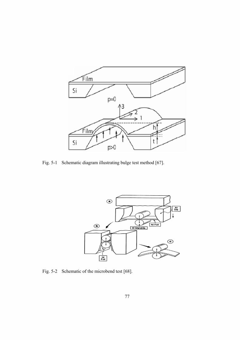
77
Fig. 5-1 Schematic diagram illustrating bulge test method [67].
Fig. 5-2 Schematic of the microbend test [68].
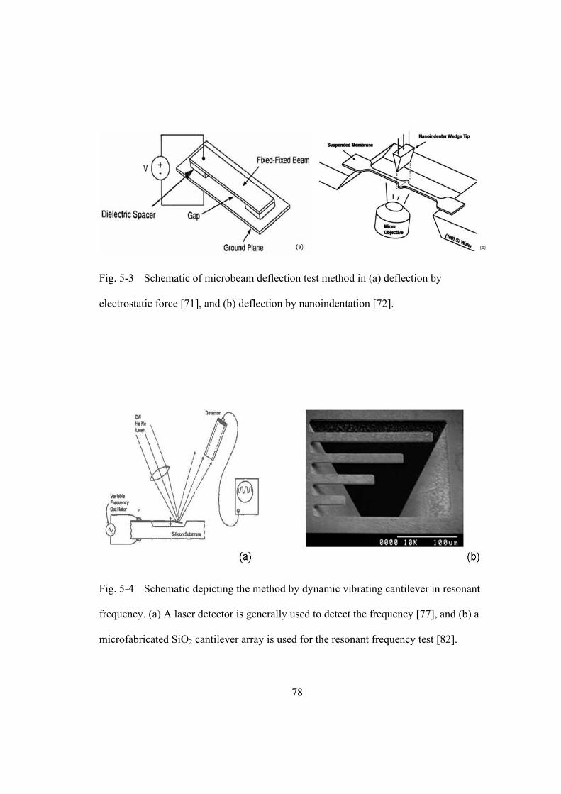
78
Fig. 5-3 Schematic of microbeam deflection test method in (a) deflection by
electrostatic force [71], and (b) deflection by nanoindentation [72].
Fig. 5-4 Schematic depicting the method by dynamic vibrating cantilever in resonant
frequency. (a) A laser detector is generally used to detect the frequency [77], and (b) a
microfabricated SiO2 cantilever array is used for the resonant frequency test [82].
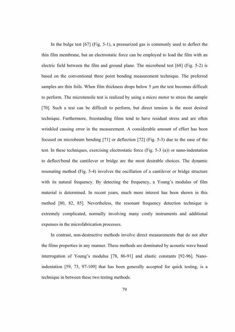
79
In the bulge test [67] (Fig. 5-1), a pressurized gas is commonly used to deflect the
thin film membrane, but an electrostatic force can be employed to load the film with an
electric field between the film and ground plane. The microbend test [68] (Fig. 5-2) is
based on the conventional three point bending measurement technique. The preferred
samples are thin foils. When film thickness drops below 5 µm the test becomes difficult
to perform. The microtensile test is realized by using a micro motor to stress the sample
[70]. Such a test can be difficult to perform, but direct tension is the most desired
technique. Furthermore, freestanding films tend to have residual stress and are often
wrinkled causing error in the measurement. A considerable amount of effort has been
focused on microbeam bending [71] or deflection [72] (Fig. 5-3) due to the ease of the
test. In these techniques, exercising electrostatic force (Fig. 5-3 (a)) or nano-indentation
to deflect/bend the cantilever or bridge are the most desirable choices. The dynamic
resonating method (Fig. 5-4) involves the oscillation of a cantilever or bridge structure
with its natural frequency. By detecting the frequency, a Young’s modulus of film
material is determined. In recent years, much more interest has been shown in this
method [80, 82, 85]. Nevertheless, the resonant frequency detection technique is
extremely complicated, normally involving many costly instruments and additional
expenses in the microfabrication processes.
In contrast, non-destructive methods involve direct measurements that do not alter
the films properties in any manner. These methods are dominated by acoustic wave based
interrogation of Young’s modulus [78, 86-91] and elastic constants [92-96]. Nano-
indentation [59, 73, 97-109] that has been generally accepted for quick testing, is a
technique in between these two testing methods.
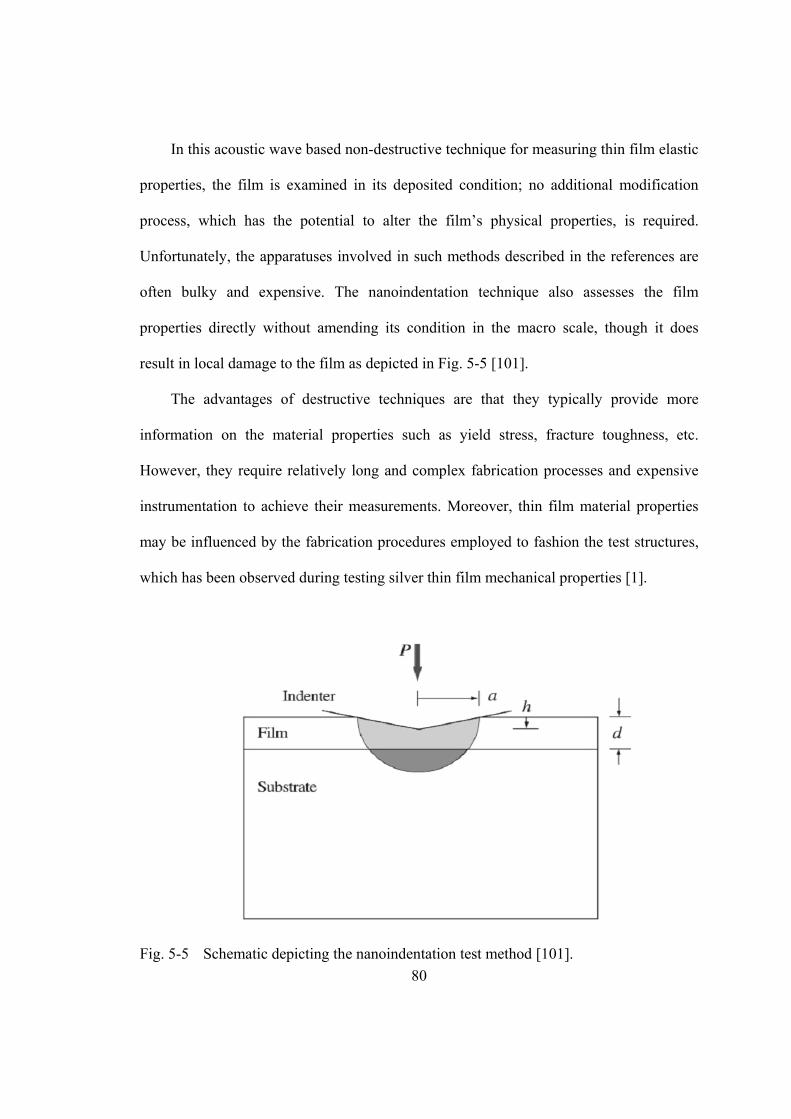
80
In this acoustic wave based non-destructive technique for measuring thin film elastic
properties, the film is examined in its deposited condition; no additional modification
process, which has the potential to alter the film’s physical properties, is required.
Unfortunately, the apparatuses involved in such methods described in the references are
often bulky and expensive. The nanoindentation technique also assesses the film
properties directly without amending its condition in the macro scale, though it does
result in local damage to the film as depicted in Fig. 5-5 [101].
The advantages of destructive techniques are that they typically provide more
information on the material properties such as yield stress, fracture toughness, etc.
However, they require relatively long and complex fabrication processes and expensive
instrumentation to achieve their measurements. Moreover, thin film material properties
may be influenced by the fabrication procedures employed to fashion the test structures,
which has been observed during testing silver thin film mechanical properties [1].
Fig. 5-5 Schematic depicting the nanoindentation test method [101].
81
On the other hand, non-destructive techniques are typically only adept at assessing
elastic properties and require sophisticated instrumentation and data reduction procedures.
Nanoindentation is able to provide both elastic and hardness properties that can be
quickly extracted from the indentation data; however, the data may be influenced by the
substrate’s properties, the indentation depth and the film thickness. In the case of porous
materials, this test may cause densification to occur, and the in other case, phase
transformation can be induced due to large hydrostatic pressure. Although numerous
reviews have been published discussing the influence of the techniques and the materials’
size on their mechanical properties [59, 63, 100], there is no standard technique generally
accepted by the thin film mechanics community that is simple, inexpensive and non-
destructive in assessing mechanical properties. A little known technique that employs a
magnetostrictive resonator, developed by Grimes and coworkers [31, 32], has been
shown to be adept at assessing thin film elastic properties and may be the standard
technique the community seeks, in terms of evaluating elastic properties. The technique is
simple and inexpensive to perform, requires no post deposition fabrication, and is non-
destructive in nature. This section is aimed at assessing the technique by measuring the
elastic properties of several commonly employed thin film materials and offering a
discussion of the error involved.
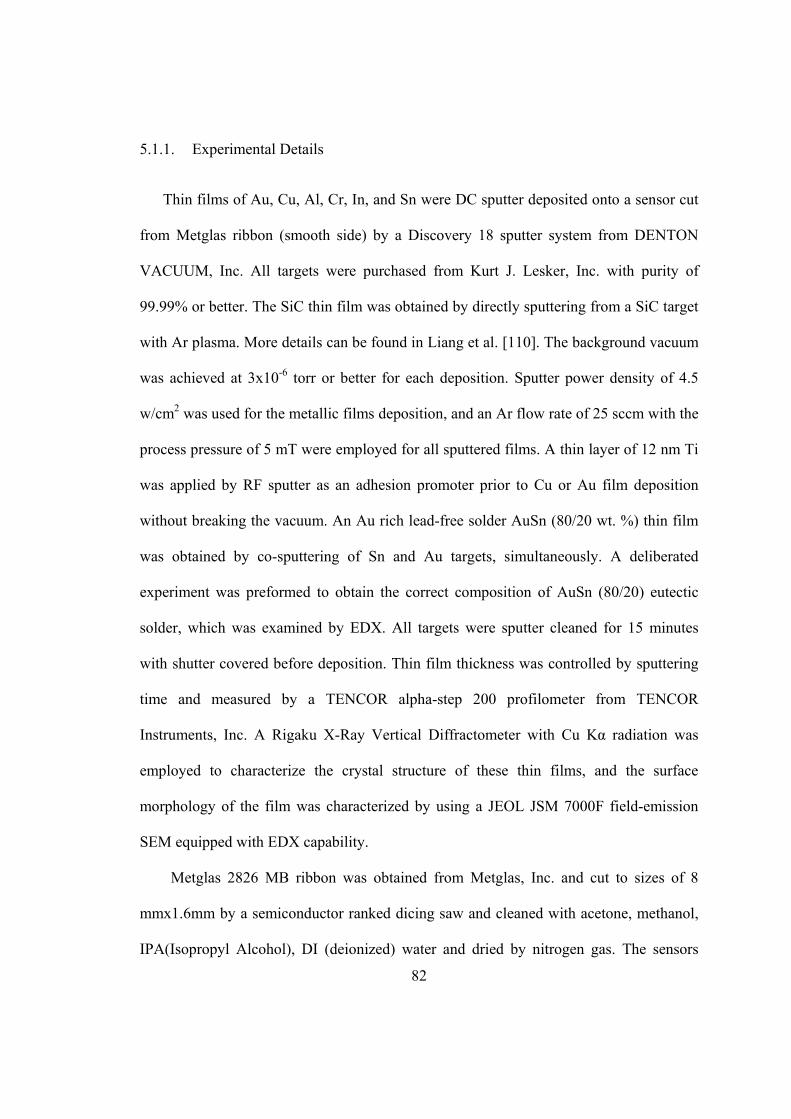
82
5.1.1. Experimental Details
Thin films of Au, Cu, Al, Cr, In, and Sn were DC sputter deposited onto a sensor cut
from Metglas ribbon (smooth side) by a Discovery 18 sputter system from DENTON
VACUUM, Inc. All targets were purchased from Kurt J. Lesker, Inc. with purity of
99.99% or better. The SiC thin film was obtained by directly sputtering from a SiC target
with Ar plasma. More details can be found in Liang et al. [110]. The background vacuum
was achieved at 3x10⁻⁶ torr or better for each deposition. Sputter power density of 4.5
w/cm2 was used for the metallic films deposition, and an Ar flow rate of 25 sccm with the
process pressure of 5 mT were employed for all sputtered films. A thin layer of 12 nm Ti
was applied by RF sputter as an adhesion promoter prior to Cu or Au film deposition
without breaking the vacuum. An Au rich lead-free solder AuSn (80/20 wt. %) thin film
was obtained by co-sputtering of Sn and Au targets, simultaneously. A deliberated
experiment was preformed to obtain the correct composition of AuSn (80/20) eutectic
solder, which was examined by EDX. All targets were sputter cleaned for 15 minutes
with shutter covered before deposition. Thin film thickness was controlled by sputtering
time and measured by a TENCOR alpha-step 200 profilometer from TENCOR
Instruments, Inc. A Rigaku X-Ray Vertical Diffractometer with Cu Kα radiation was
employed to characterize the crystal structure of these thin films, and the surface
morphology of the film was characterized by using a JEOL JSM 7000F field-emission
SEM equipped with EDX capability.
Metglas 2826 MB ribbon was obtained from Metglas, Inc. and cut to sizes of 8
mmx1.6mm by a semiconductor ranked dicing saw and cleaned with acetone, methanol,
IPA(Isopropyl Alcohol), DI (deionized) water and dried by nitrogen gas. The sensors
83
were dehydrated in a convection oven at 120oC for 20 minutes prior to use. In the case of
measuring the Au film Young’s modulus, the masses of the sensor before and after
deposition were measured immediately by a Metter-Toledo AT-20 microbalance with a
resolution of 2 µg. The method used of measuring the resonant frequency of the sensor
with or without the thin film coating was described in section 2.
5.1.2. Results and Discussion
This section details the characterization and results of deposited thin film.
Parameters such as surface morphology, crystal structure, and sensor responses to various
types of films, the determined thin films Young’s moduli and error analysis are included.
5.1.2.1. Surface Morphology of Deposited Thin Film Materials of Au, Cu, Al, Cr, In,
Sn, AuSn (80/20), and SiC
All films deposited on the magnetostrictive sensor platform exhibited continuous
surface coverage and excellent adhesion as no delimitation or pits were observed during
SEM characterization. This is a good indication that the numerical solution can assume
that film and sensor undergo the same amount of straining during vibration testing.
Deposited Au and Cu films possessed very fine grain sizes/particles as shown in Fig. 5-6
(a) and (c). The grain size of the Cr exhibited sawfish likeness or star shapes with even
morphology as shown in Fig. 5-6 (d), which have been commonly observed by other
researchers [111]. The low-melting-temperature materials, the In, Sn, and Al films,
exhibited considerable large grain sizes/particles and appeared somewhat porous, (Fig. 5-
6 (b), (e) and (f)). Furthermore, indium and tin films possessed a random island texture
84
and relatively rough surface. The Sn film also had whiskers on its surface approximately
1.0 µm long as seen in the Fig. 5-7(h). These whiskers are often observed in electronic
packaging and assembly but are also found by other researchers in sputter deposition
processes [112] and are likely due to relief of compress stress in the film. Finally, the
AuSn (80/20) eutectic solder yielded the most unusual of the microstructure, (see Fig. 5-6
g). No large islands were seen as in the pure Sn film, likely due to alloying with Au
atoms. As was seen in the SEM image, the surface became flusher and developed into
interlaced structures.
As deposited gold films of various thicknesses were examined under SEM. Uniform
particle sizes of the Au coating were clearly developed on the sensor platform whose size
scaled with the film thickness, (see Fig. 5-7). Complete surface coverage was observed
even at film thickness as thin as 100 nm. The particle size increase with film thickness
was likely a result from increased thermal energy induced and the large number of Au
atoms available for aggregation for thicker film [113]. Also, note that the deposition of
thicker Au film requires the longer processing time; consequently, a higher temperature
on substrates may result from additional commission of ions and atoms. However, when
the film thickness became thicker than 0.855 µm, the grain size remained relatively
constant. The highest substrate temperature recorded during the sputtering process for
different thin film thicknesses is listed in Table 5-1. Similar occurrences were observed
for other materials during sputter deposition, but all exhibited lower temperatures than
that for Au, likely a result from the sputter yield of Au being the highest among all films
grown.
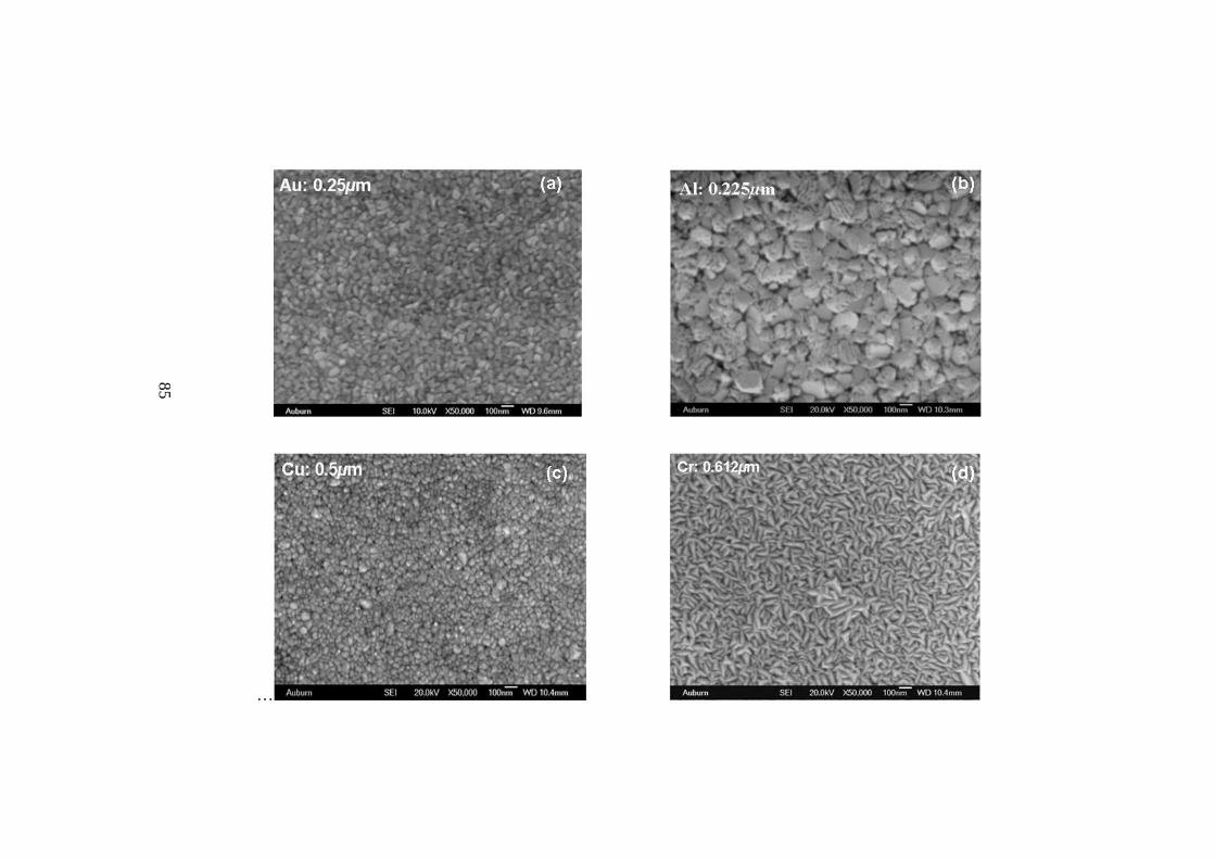
85
…
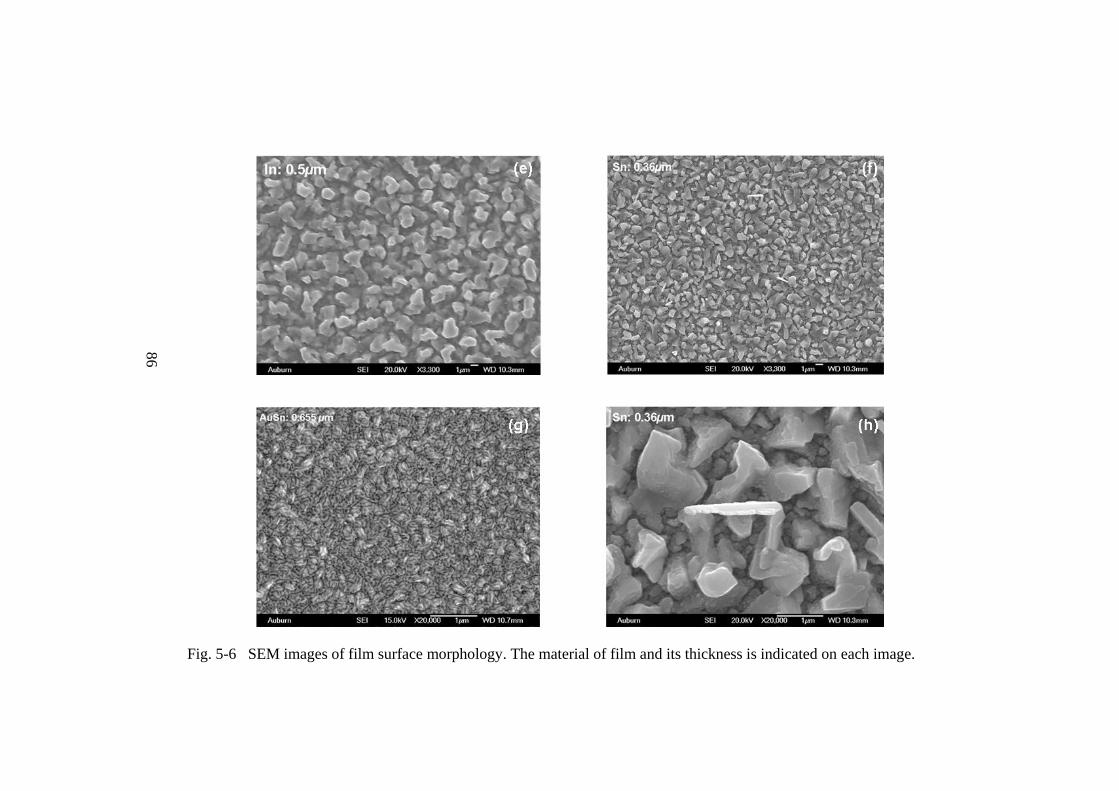
86
Fig. 5-6 SEM images of film surface morphology. The material of film and its thickness is indicated on each image.
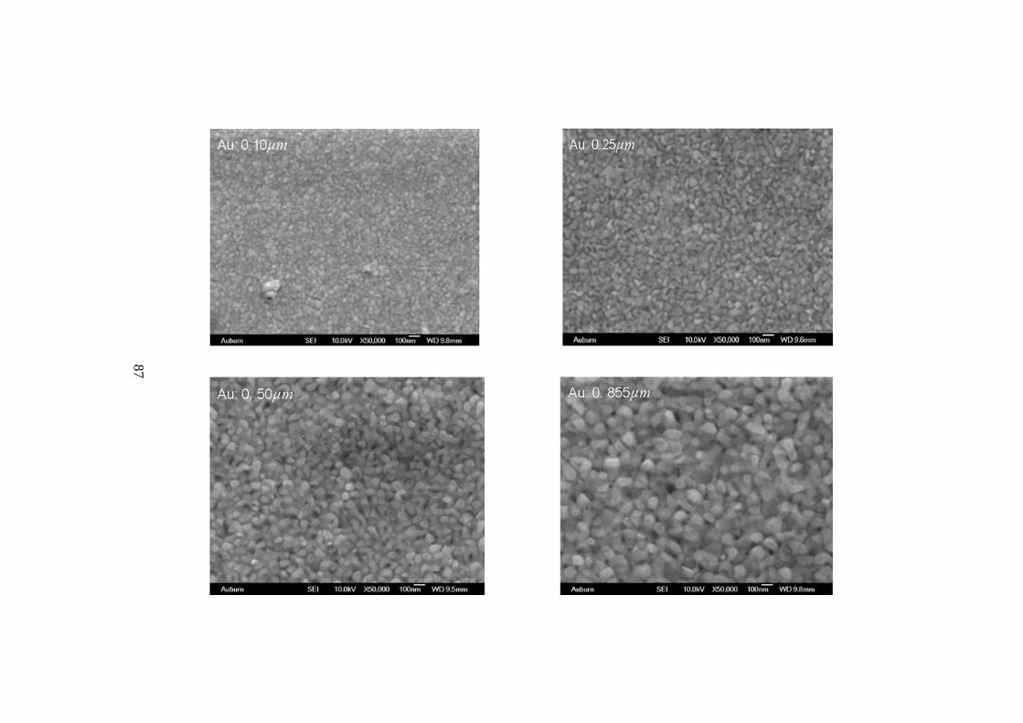
87
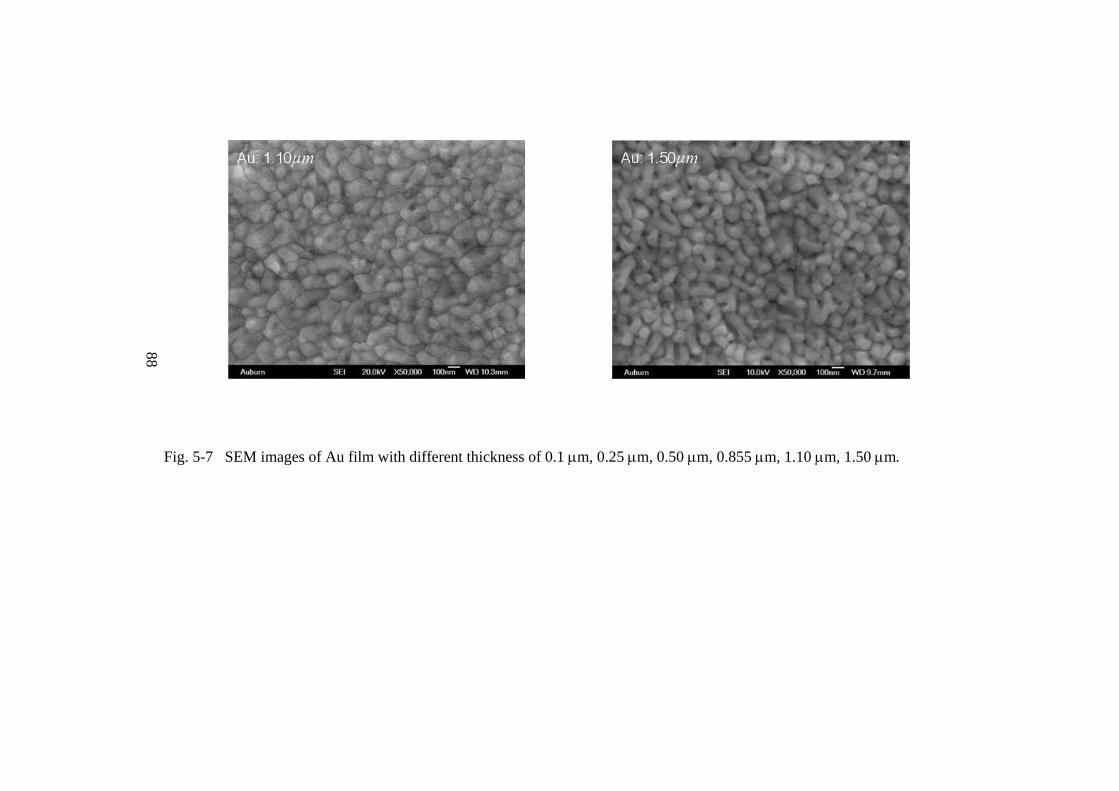
88
Fig. 5-7 SEM images of Au film with different thickness of 0.1 µm, 0.25 µm, 0.50 µm, 0.855 µm, 1.10 µm, 1.50 µm.
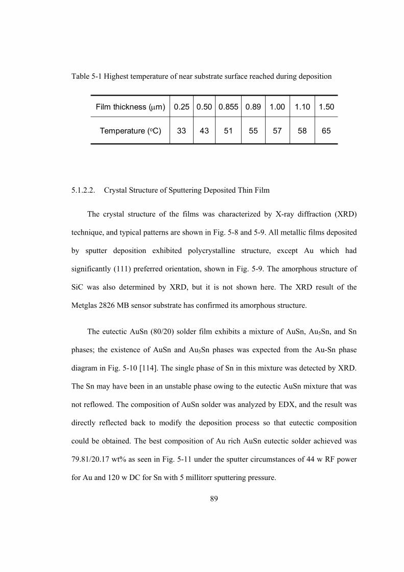
89
Table 5-1 Highest temperature of near substrate surface reached during deposition
58
1.10
65
1.50
57
1.00
55
0.89
51
0.855
43
0.50
33
0.25
Temperature (oC)
Film thickness (µm)
5.1.2.2. Crystal Structure of Sputtering Deposited Thin Film
The crystal structure of the films was characterized by X-ray diffraction (XRD)
technique, and typical patterns are shown in Fig. 5-8 and 5-9. All metallic films deposited
by sputter deposition exhibited polycrystalline structure, except Au which had
significantly (111) preferred orientation, shown in Fig. 5-9. The amorphous structure of
SiC was also determined by XRD, but it is not shown here. The XRD result of the
Metglas 2826 MB sensor substrate has confirmed its amorphous structure.
The eutectic AuSn (80/20) solder film exhibits a mixture of AuSn, Au5Sn, and Sn
phases; the existence of AuSn and Au5Sn phases was expected from the Au-Sn phase
diagram in Fig. 5-10 [114]. The single phase of Sn in this mixture was detected by XRD.
The Sn may have been in an unstable phase owing to the eutectic AuSn mixture that was
not reflowed. The composition of AuSn solder was analyzed by EDX, and the result was
directly reflected back to modify the deposition process so that eutectic composition
could be obtained. The best composition of Au rich AuSn eutectic solder achieved was
79.81/20.17 wt% as seen in Fig. 5-11 under the sputter circumstances of 44 w RF power
for Au and 120 w DC for Sn with 5 millitorr sputtering pressure.
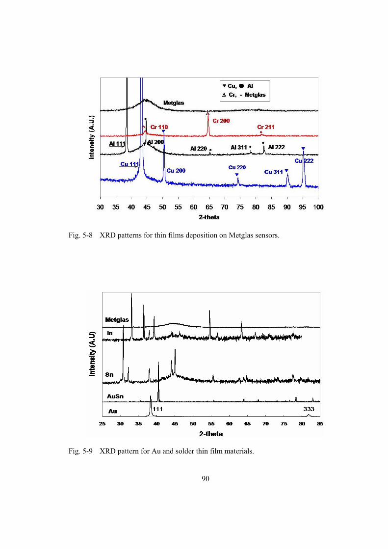
90
Fig. 5-8 XRD patterns for thin films deposition on Metglas sensors.
Fig. 5-9 XRD pattern for Au and solder thin film materials.
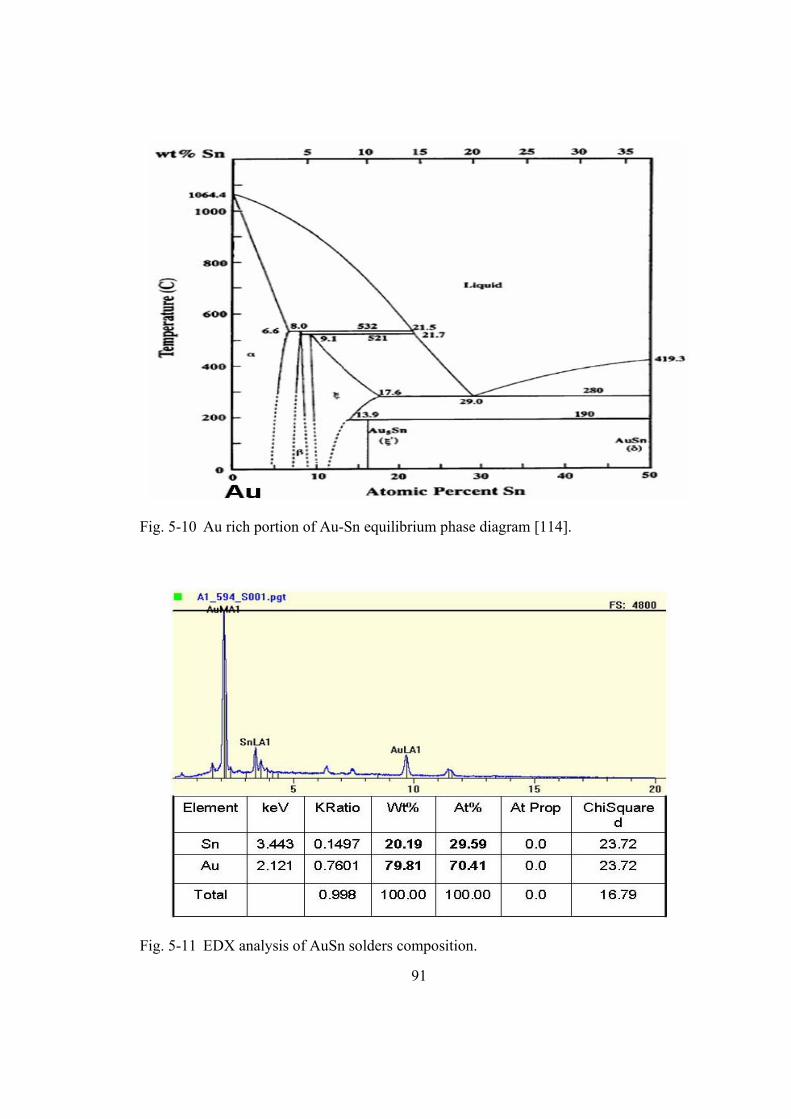
91
Fig. 5-10 Au rich portion of Au-Sn equilibrium phase diagram [114].
Fig. 5-11 EDX analysis of AuSn solders composition.
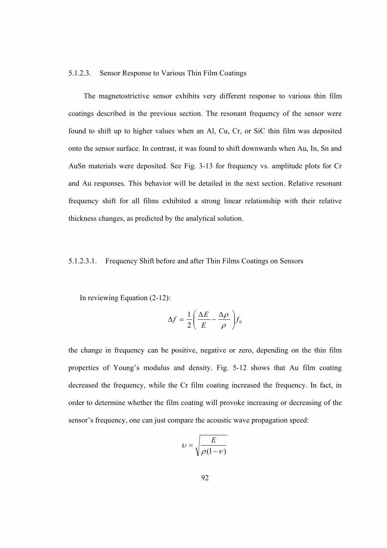
92
5.1.2.3. Sensor Response to Various Thin Film Coatings
The magnetostrictive sensor exhibits very different response to various thin film
coatings described in the previous section. The resonant frequency of the sensor were
found to shift up to higher values when an Al, Cu, Cr, or SiC thin film was deposited
onto the sensor surface. In contrast, it was found to shift downwards when Au, In, Sn and
AuSn materials were deposited. See Fig. 3-13 for frequency vs. amplitude plots for Cr
and Au responses. This behavior will be detailed in the next section. Relative resonant
frequency shift for all films exhibited a strong linear relationship with their relative
thickness changes, as predicted by the analytical solution.
5.1.2.3.1. Frequency Shift before and after Thin Films Coatings on Sensors
In reviewing Equation (2-12):
the change in frequency can be positive, negative or zero, depending on the thin film
properties of Young’s modulus and density. Fig. 5-12 shows that Au film coating
decreased the frequency, while the Cr film coating increased the frequency. In fact, in
order to determine whether the film coating will provoke increasing or decreasing of the
sensor’s frequency, one can just compare the acoustic wave propagation speed:
)1( νρυ
−=
E
021 f
EEf ⎟⎟
⎠
⎞⎜⎜⎝
⎛ ∆−
∆=∆
ρρ
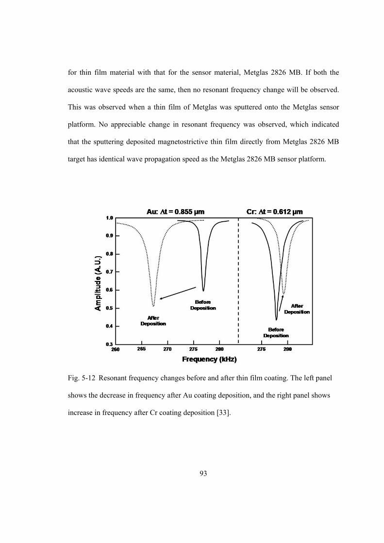
93
for thin film material with that for the sensor material, Metglas 2826 MB. If both the
acoustic wave speeds are the same, then no resonant frequency change will be observed.
This was observed when a thin film of Metglas was sputtered onto the Metglas sensor
platform. No appreciable change in resonant frequency was observed, which indicated
that the sputtering deposited magnetostrictive thin film directly from Metglas 2826 MB
target has identical wave propagation speed as the Metglas 2826 MB sensor platform.
Fig. 5-12 Resonant frequency changes before and after thin film coating. The left panel
shows the decrease in frequency after Au coating deposition, and the right panel shows
increase in frequency after Cr coating deposition [33].
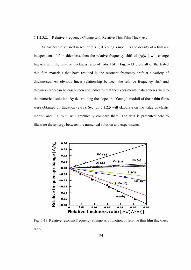
94
5.1.2.3.2. Relative Frequency Change with Relative Thin Film Thickness
As has been discussed in section 2.3.1, if Young’s modulus and density of a film are
independent of film thickness, then the relative frequency shift of (∆f/f0 ) will change
linearly with the relative thickness ratio of [∆t/(t+∆t)]. Fig. 5-13 plots all of the tested
thin film materials that have resulted in the resonant frequency shift at a variety of
thicknesses. An obvious linear relationship between the relative frequency shift and
thickness ratio can be easily seen and indicates that the experimental data adheres well to
the numerical solution. By determining the slope, the Young’s moduli of those thin films
were obtained by Equation (2-18). Section 5.1.2.5 will elaborate on the value of elastic
moduli and Fig. 5-21 will graphically compare them. The data is presented here to
illustrate the synergy between the numerical solution and experiments.
Fig. 5-13 Relative resonant frequency change as a function of relative thin film thickness
ratio.
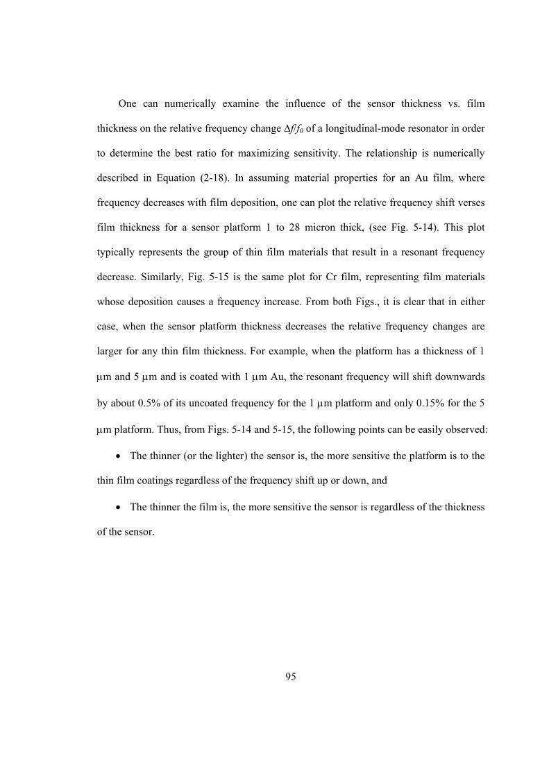
95
One can numerically examine the influence of the sensor thickness vs. film
thickness on the relative frequency change ∆f/f0 of a longitudinal-mode resonator in order
to determine the best ratio for maximizing sensitivity. The relationship is numerically
described in Equation (2-18). In assuming material properties for an Au film, where
frequency decreases with film deposition, one can plot the relative frequency shift verses
film thickness for a sensor platform 1 to 28 micron thick, (see Fig. 5-14). This plot
typically represents the group of thin film materials that result in a resonant frequency
decrease. Similarly, Fig. 5-15 is the same plot for Cr film, representing film materials
whose deposition causes a frequency increase. From both Figs., it is clear that in either
case, when the sensor platform thickness decreases the relative frequency changes are
larger for any thin film thickness. For example, when the platform has a thickness of 1
µm and 5 µm and is coated with 1 µm Au, the resonant frequency will shift downwards
by about 0.5% of its uncoated frequency for the 1 µm platform and only 0.15% for the 5
µm platform. Thus, from Figs. 5-14 and 5-15, the following points can be easily observed:
• The thinner (or the lighter) the sensor is, the more sensitive the platform is to the
thin film coatings regardless of the frequency shift up or down, and
• The thinner the film is, the more sensitive the sensor is regardless of the thickness
of the sensor.
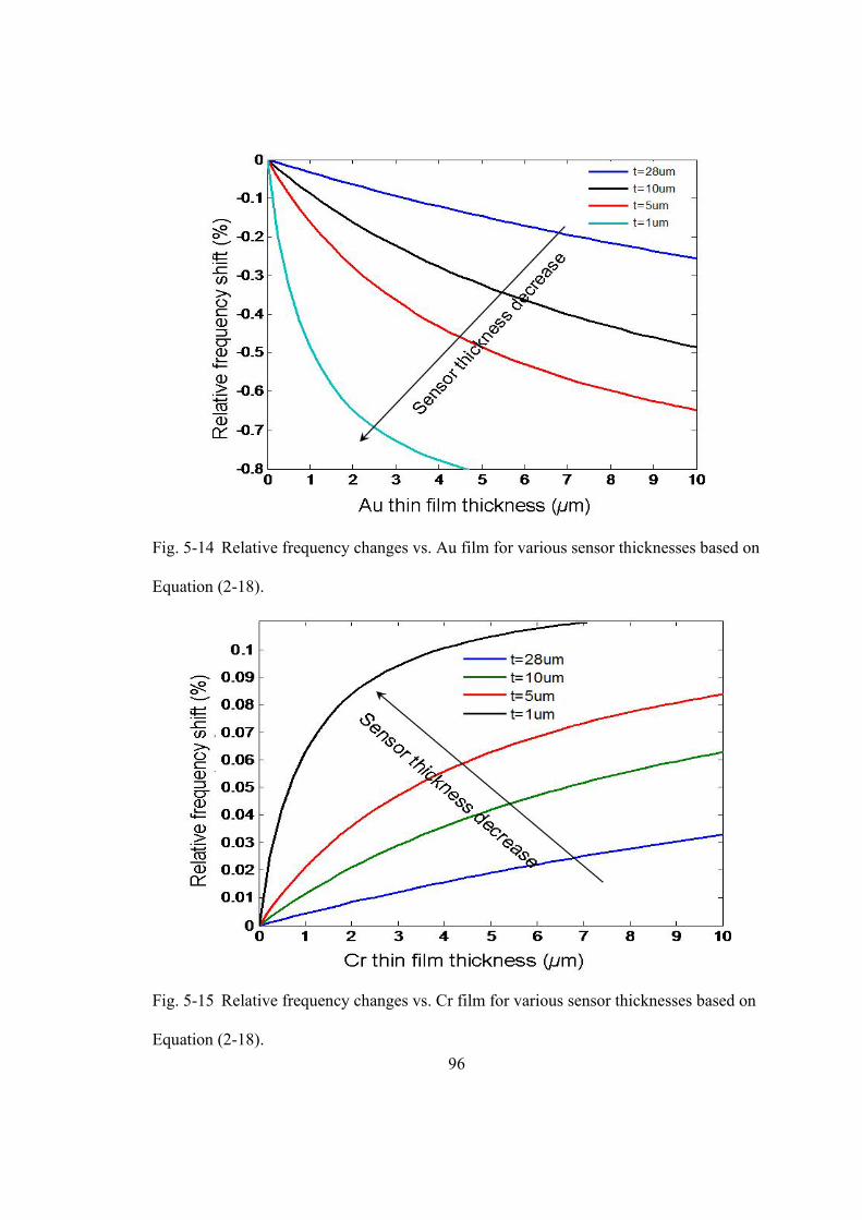
96
Fig. 5-14 Relative frequency changes vs. Au film for various sensor thicknesses based on
Equation (2-18).
Fig. 5-15 Relative frequency changes vs. Cr film for various sensor thicknesses based on
Equation (2-18).
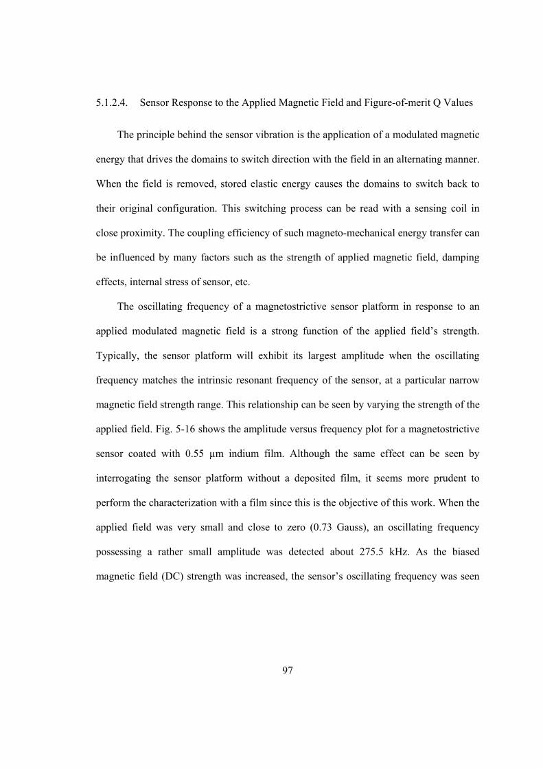
97
5.1.2.4. Sensor Response to the Applied Magnetic Field and Figure-of-merit Q Values
The principle behind the sensor vibration is the application of a modulated magnetic
energy that drives the domains to switch direction with the field in an alternating manner.
When the field is removed, stored elastic energy causes the domains to switch back to
their original configuration. This switching process can be read with a sensing coil in
close proximity. The coupling efficiency of such magneto-mechanical energy transfer can
be influenced by many factors such as the strength of applied magnetic field, damping
effects, internal stress of sensor, etc.
The oscillating frequency of a magnetostrictive sensor platform in response to an
applied modulated magnetic field is a strong function of the applied field’s strength.
Typically, the sensor platform will exhibit its largest amplitude when the oscillating
frequency matches the intrinsic resonant frequency of the sensor, at a particular narrow
magnetic field strength range. This relationship can be seen by varying the strength of the
applied field. Fig. 5-16 shows the amplitude versus frequency plot for a magnetostrictive
sensor coated with 0.55 µm indium film. Although the same effect can be seen by
interrogating the sensor platform without a deposited film, it seems more prudent to
perform the characterization with a film since this is the objective of this work. When the
applied field was very small and close to zero (0.73 Gauss), an oscillating frequency
possessing a rather small amplitude was detected about 275.5 kHz. As the biased
magnetic field (DC) strength was increased, the sensor’s oscillating frequency was seen
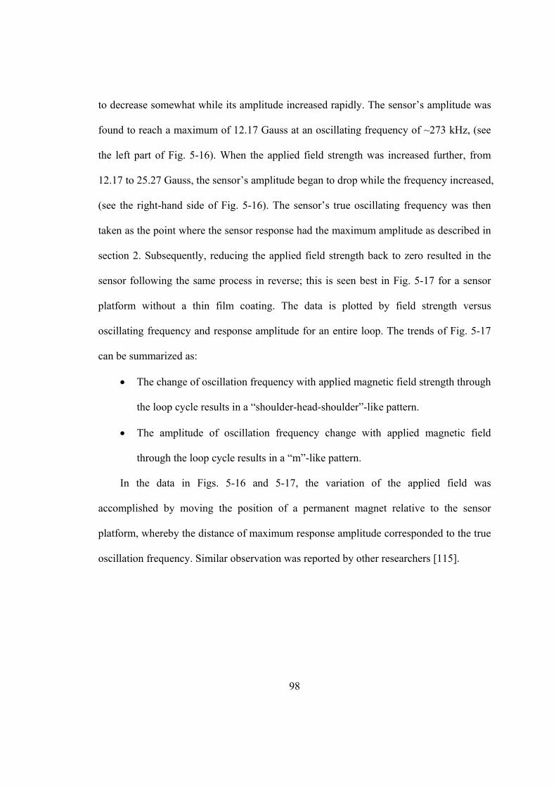
98
to decrease somewhat while its amplitude increased rapidly. The sensor’s amplitude was
found to reach a maximum of 12.17 Gauss at an oscillating frequency of ~273 kHz, (see
the left part of Fig. 5-16). When the applied field strength was increased further, from
12.17 to 25.27 Gauss, the sensor’s amplitude began to drop while the frequency increased,
(see the right-hand side of Fig. 5-16). The sensor’s true oscillating frequency was then
taken as the point where the sensor response had the maximum amplitude as described in
section 2. Subsequently, reducing the applied field strength back to zero resulted in the
sensor following the same process in reverse; this is seen best in Fig. 5-17 for a sensor
platform without a thin film coating. The data is plotted by field strength versus
oscillating frequency and response amplitude for an entire loop. The trends of Fig. 5-17
can be summarized as:
• The change of oscillation frequency with applied magnetic field strength through
the loop cycle results in a “shoulder-head-shoulder”-like pattern.
• The amplitude of oscillation frequency change with applied magnetic field
through the loop cycle results in a “m”-like pattern.
In the data in Figs. 5-16 and 5-17, the variation of the applied field was
accomplished by moving the position of a permanent magnet relative to the sensor
platform, whereby the distance of maximum response amplitude corresponded to the true
oscillation frequency. Similar observation was reported by other researchers [115].
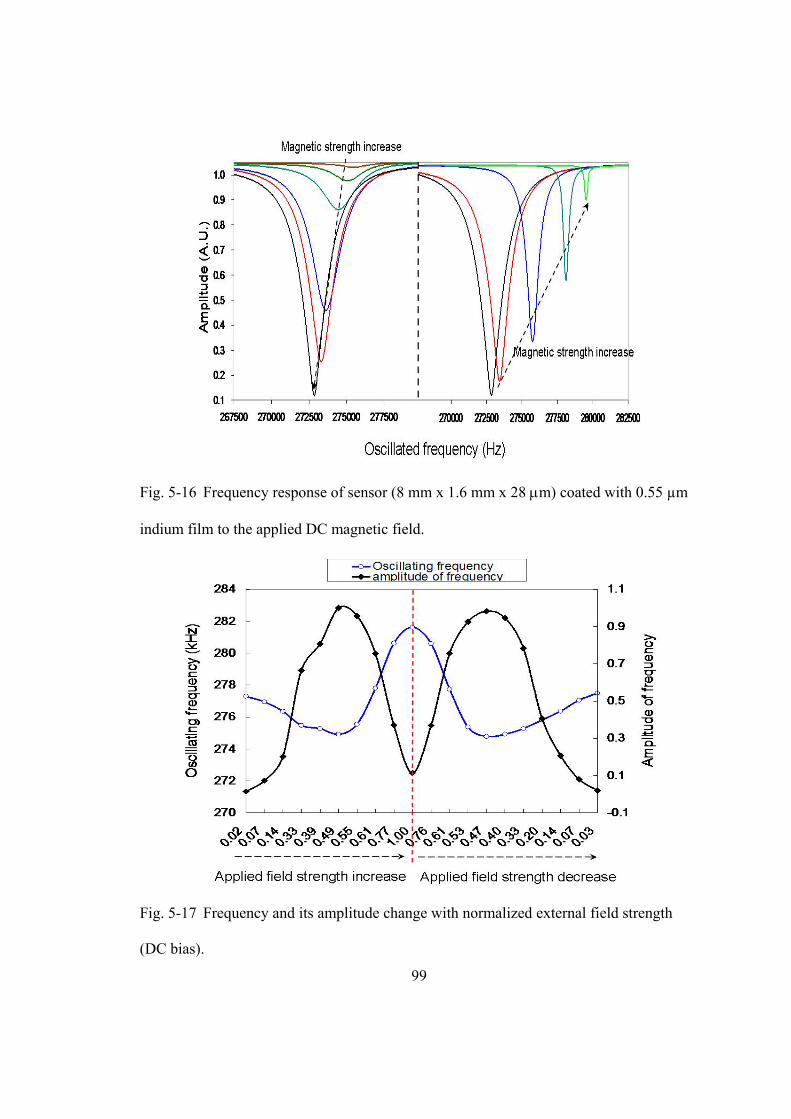
99
Fig. 5-16 Frequency response of sensor (8 mm x 1.6 mm x 28 µm) coated with 0.55 µm
indium film to the applied DC magnetic field.
Fig. 5-17 Frequency and its amplitude change with normalized external field strength
(DC bias).
100
The resonant frequency response peaks all exhibited different degrees of peak
amplitude and sharpness. In order to determine the relative quality of these peaks it is
necessary to use the quality factor (Q-factor), which is commonly used to examine the
energy dissipation in microelectronics mechanical systems. Physically, the Q-factor
represents the total energy lost per cycle of a vibration system and can be defined as [116,
117]:
(5-1)
where w0 and ∆w are stored vibration energy and total lost energy per cycle, respectively.
This Q-factor can be calculated by analysis of the spectrum of resonant frequency. It is
generally called as figure-of-merit, a numerical quantity based on one or more
characteristics of a system or device that represents a measure of efficiency or
effectiveness. Figure-of-merit can be experimentally determined as a ratio of the
resonance frequency f0 to the width (∆f) of the resonance peak at its half amplitude, and
expressed as
(5-2)
The Q-factor of a vibration system is dependent on many factors such as material
properties, medium of operation, etc.
The Q-factor for the data in Fig. 5-16 and 5-17 can then be calculated bases upon
Equation (5-2), which is plotted in Fig. 5-18 as Q-factor versus normalized applied field
for a platform both with and without the indium film. The Q values for each sensor were
found to be around 265 and to be very close to each other at their resonant frequency. At
applied fields below the resonant frequency, the Q values were found to be 200, (see Fig.
ffQ∆
= 0
⎟⎠⎞
⎜⎝⎛∆
=w
wQ 02π
101
5-18). At applied fields above the resonant frequency, the curves begin to differ with the
uncoated platform possessing larger Q values. However, it is likely the Q-factor is a
function of the type of film and its thickness, (see Fig. 5-19), where the Q value increases
from 430 to 710 when the Cu thickness increases from 0.5 µm to 1.23 µm. A similar
tendency is also seen in the case of the sensor with Cr coating, Fig. 5-20. Furthermore,
Fig. 5-20 also indicates that films with higher Young’s modulus seem to yield a higher Q
value. As will be shown in next section, the Cu film material possessed a higher Young’s
modulus than the Cr film. Nevertheless, the Q value for a sensor with thin film coating is
found to increase as film Young’s modulus or film thickness are increased. In both cases
the increase in effective elastic modulus of the vibrating system, when the film modulus
was higher than that of the substrate, resulted in an increased Q-factor, which follow well
with Equation (5-2). Furthermore, along with the Q-factor, the effective resonant
frequency was found to increase as the film thickness increased. Such an increase in the
Q-factor with increasing resonant frequency is mathematically confirmed for a cantilever
vibrating in the transverse mode [116].
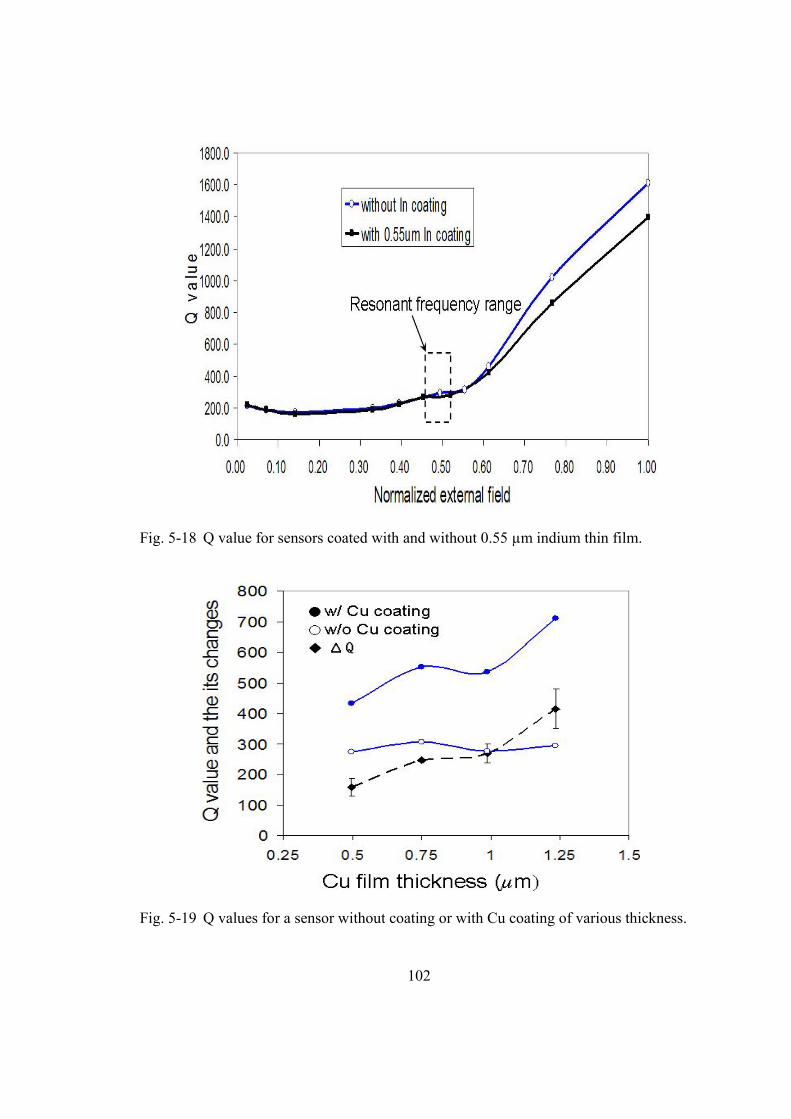
102
Fig. 5-18 Q value for sensors coated with and without 0.55 µm indium thin film.
Fig. 5-19 Q values for a sensor without coating or with Cu coating of various thickness.
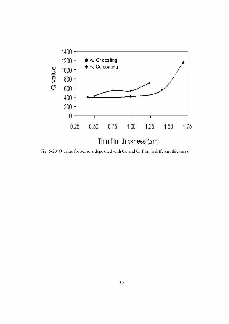
103
Fig. 5-20 Q value for sensors deposited with Cu and Cr film in different thickness.
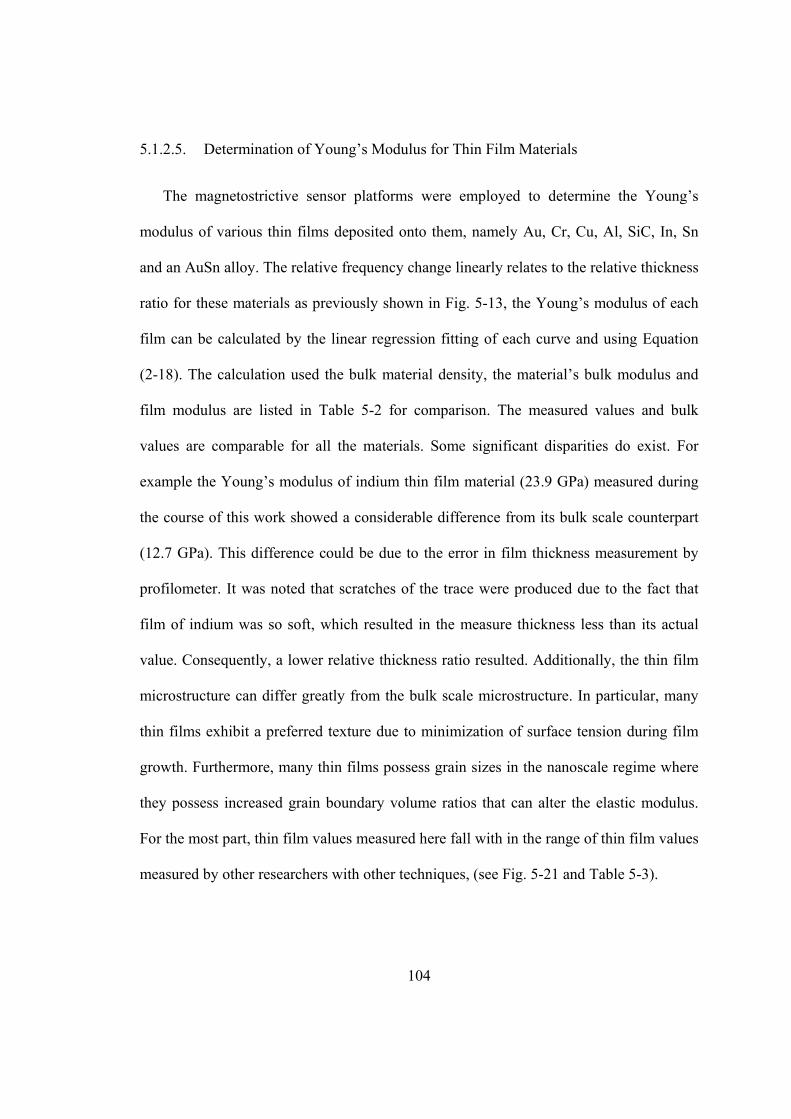
104
5.1.2.5. Determination of Young’s Modulus for Thin Film Materials
The magnetostrictive sensor platforms were employed to determine the Young’s
modulus of various thin films deposited onto them, namely Au, Cr, Cu, Al, SiC, In, Sn
and an AuSn alloy. The relative frequency change linearly relates to the relative thickness
ratio for these materials as previously shown in Fig. 5-13, the Young’s modulus of each
film can be calculated by the linear regression fitting of each curve and using Equation
(2-18). The calculation used the bulk material density, the material’s bulk modulus and
film modulus are listed in Table 5-2 for comparison. The measured values and bulk
values are comparable for all the materials. Some significant disparities do exist. For
example the Young’s modulus of indium thin film material (23.9 GPa) measured during
the course of this work showed a considerable difference from its bulk scale counterpart
(12.7 GPa). This difference could be due to the error in film thickness measurement by
profilometer. It was noted that scratches of the trace were produced due to the fact that
film of indium was so soft, which resulted in the measure thickness less than its actual
value. Consequently, a lower relative thickness ratio resulted. Additionally, the thin film
microstructure can differ greatly from the bulk scale microstructure. In particular, many
thin films exhibit a preferred texture due to minimization of surface tension during film
growth. Furthermore, many thin films possess grain sizes in the nanoscale regime where
they possess increased grain boundary volume ratios that can alter the elastic modulus.
For the most part, thin film values measured here fall with in the range of thin film values
measured by other researchers with other techniques, (see Fig. 5-21 and Table 5-3).
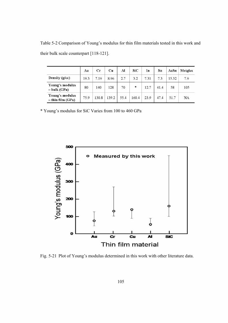
105
Table 5-2 Comparison of Young’s modulus for thin film materials tested in this work and
their bulk scale counterpart [118-121].
* Young’s modulus for SiC Varies from 100 to 460 GPa
Fig. 5-21 Plot of Young’s modulus determined in this work with other literature data.
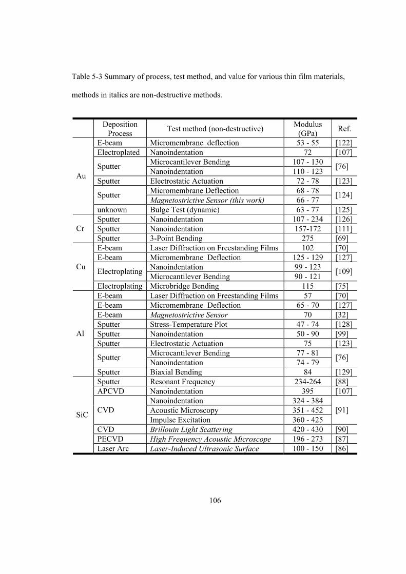
106
Table 5-3 Summary of process, test method, and value for various thin film materials,
methods in italics are non-destructive methods.
Deposition Process Test method (non-destructive) Modulus
(GPa) Ref.
E-beam Micromembrane deflection 53 - 55 [122]Electroplated Nanoindentation 72 [107]
Microcantilever Bending 107 - 130 Sputter Nanoindentation 110 - 123 [76]
Sputter Electrostatic Actuation 72 - 78 [123]Micromembrane Deflection 68 - 78 Sputter Magnetostrictive Sensor (this work) 66 - 77 [124]
Au
unknown Bulge Test (dynamic) 63 - 77 [125]Sputter Nanoindentation 107 - 234 [126]Sputter Nanoindentation 157-172 [111]Cr Sputter 3-Point Bending 275 [69]E-beam Laser Diffraction on Freestanding Films 102 [70]E-beam Micromembrane Deflection 125 - 129 [127]
Nanoindentation 99 - 123 Electroplating Microcantilever Bending 90 - 121 [109]Cu
Electroplating Microbridge Bending 115 [75]E-beam Laser Diffraction on Freestanding Films 57 [70]E-beam Micromembrane Deflection 65 - 70 [127]E-beam Magnetostrictive Sensor 70 [32]Sputter Stress-Temperature Plot 47 - 74 [128]Sputter Nanoindentation 50 - 90 [99]Sputter Electrostatic Actuation 75 [123]
Microcantilever Bending 77 - 81 Sputter Nanoindentation 74 - 79 [76]
Al
Sputter Biaxial Bending 84 [129]Sputter Resonant Frequency 234-264 [88]APCVD Nanoindentation 395 [107]
Nanoindentation 324 - 384 Acoustic Microscopy 351 - 452 CVD Impulse Excitation 360 - 425
[91]
CVD Brillouin Light Scattering 420 - 430 [90]PECVD High Frequency Acoustic Microscope 196 - 273 [87]
SiC
Laser Arc Laser-Induced Ultrasonic Surface 100 - 150 [86]
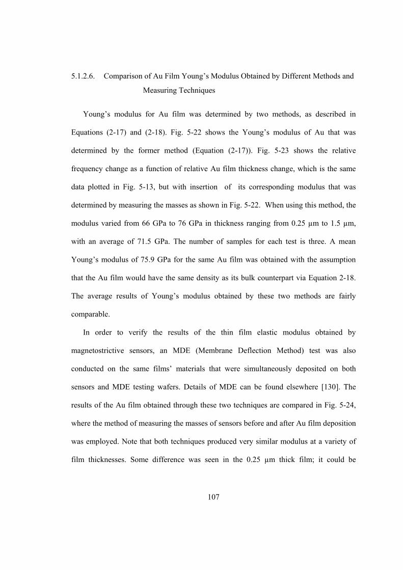
107
5.1.2.6. Comparison of Au Film Young’s Modulus Obtained by Different Methods and
Measuring Techniques
Young’s modulus for Au film was determined by two methods, as described in
Equations (2-17) and (2-18). Fig. 5-22 shows the Young’s modulus of Au that was
determined by the former method (Equation (2-17)). Fig. 5-23 shows the relative
frequency change as a function of relative Au film thickness change, which is the same
data plotted in Fig. 5-13, but with insertion of its corresponding modulus that was
determined by measuring the masses as shown in Fig. 5-22. When using this method, the
modulus varied from 66 GPa to 76 GPa in thickness ranging from 0.25 µm to 1.5 µm,
with an average of 71.5 GPa. The number of samples for each test is three. A mean
Young’s modulus of 75.9 GPa for the same Au film was obtained with the assumption
that the Au film would have the same density as its bulk counterpart via Equation 2-18.
The average results of Young’s modulus obtained by these two methods are fairly
comparable.
In order to verify the results of the thin film elastic modulus obtained by
magnetostrictive sensors, an MDE (Membrane Deflection Method) test was also
conducted on the same films’ materials that were simultaneously deposited on both
sensors and MDE testing wafers. Details of MDE can be found elsewhere [130]. The
results of the Au film obtained through these two techniques are compared in Fig. 5-24,
where the method of measuring the masses of sensors before and after Au film deposition
was employed. Note that both techniques produced very similar modulus at a variety of
film thicknesses. Some difference was seen in the 0.25 µm thick film; it could be
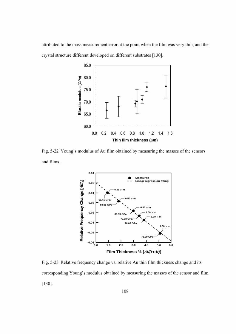
108
attributed to the mass measurement error at the point when the film was very thin, and the
crystal structure different developed on different substrates [130].
60.0
65.0
70.0
75.0
80.0
85.0
0.0 0.2 0.4 0.6 0.8 1.0 1.2 1.4 1.6Thin film thickness (µm)
Elas
ticm
odul
us(G
Pa)
Fig. 5-22 Young’s modulus of Au film obtained by measuring the masses of the sensors
and films.
Rel
ativ
e Fr
eque
ncy
Chan
ge [∆
f/f0]
Film Thickness % [∆t/(t+∆t)]
3.01.00.0 2.0
0.00
5.0 6.0
MeasuredLinear regression fitting
0.01
-0.01
-0.02
-0.03
-0.04
-0.05
-0.06
66.41 GPa
4.0
68.08 GPa
69.33 GPa
70.98 GPa
76.05 GPa
76.29 GPa
0.25 μm
0.50 μm
0.85 μm
1.00 μm
1.10 μm
1.50 μm
Fig. 5-23 Relative frequency change vs. relative Au thin film thickness change and its
corresponding Young’s modulus obtained by measuring the masses of the sensor and film
[130].
109
Youn
g’s
Mod
ulus
(GPa
)
Film Thickness (µm)
0.800.200 1.400.60
60
0
100
1.601.00
Magnetostrictive Sensor
0.40 1.20
70
80
90Membrane Deflection Experiment
Fig. 5-24 Young’s modulus of Au film measured at different thickness by magnetostric-
tive sensor and MDE [130].
5.1.2.7. Finite Element Analysis to Verify Thin Film Young’s Modulus Measurement
The preceding sections demonstrated that a Metglas strip could be easily employed to
measure the thin film Young’s modulus. Although an alternative technique was used to
verify the measurements, it is prudent to also perform numerical simulations as an
additional counter check. In this regard, an element size of 160 µm x 160 µm x 5.6 µm
was used for mode meshing 8 mm x 1.6 mm sensors. Fig. 5-25 represents the mesh
model of a sensor with an Au coating on top. The materials’ properties used in the
simulation are listed in Table 5-4. Sensors coated with a Au film with the thicknesses of
0.25 µm, 0.40 µm, 0.50 µm, 0.855 µm, 0.89 µm, 1.00 µm, 1.10 µm and 1.5 µm were
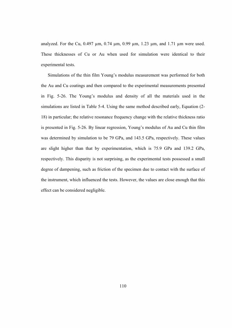
110
analyzed. For the Cu, 0.497 µm, 0.74 µm, 0.99 µm, 1.23 µm, and 1.71 µm were used.
These thicknesses of Cu or Au when used for simulation were identical to their
experimental tests.
Simulations of the thin film Young’s modulus measurement was performed for both
the Au and Cu coatings and then compared to the experimental measurements presented
in Fig. 5-26. The Young’s modulus and density of all the materials used in the
simulations are listed in Table 5-4. Using the same method described early, Equation (2-
18) in particular; the relative resonance frequency change with the relative thickness ratio
is presented in Fig. 5-26. By linear regression, Young’s modulus of Au and Cu thin film
was determined by simulation to be 79 GPa, and 143.5 GPa, respectively. These values
are slight higher than that by experimentation, which is 75.9 GPa and 139.2 GPa,
respectively. This disparity is not surprising, as the experimental tests possessed a small
degree of dampening, such as friction of the specimen due to contact with the surface of
the instrument, which influenced the tests. However, the values are close enough that this
effect can be considered negligible.
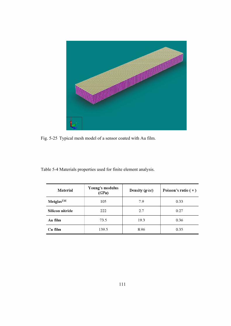
111
Fig. 5-25 Typical mesh model of a sensor coated with Au film.
Table 5-4 Materials properties used for finite element analysis.
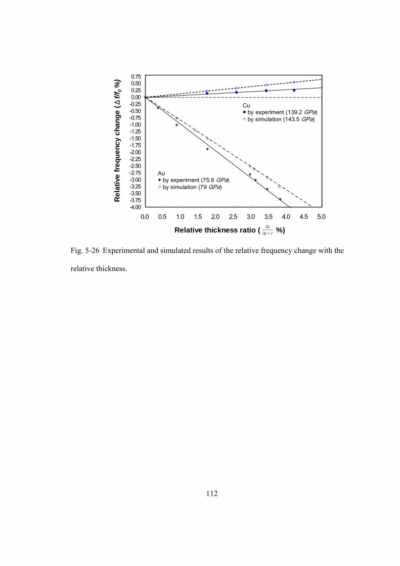
112
Rel
ativ
e fre
quen
cy c
hang
e (Δ
f/f0 %
)
-4.00-3.75-3.50-3.25-3.00-2.75-2.50-2.25-2.00-1.75-1.50-1.25-1.00-0.75-0.50-0.250.000.250.500.75
0.0 0.5 1.0 1.5 2.0 2.5 3.0 3.5 4.0 4.5 5.0
Au by experiment (75.9 GPa) by simulation (79 GPa)
Cu by experiment (139.2 GPa) by simulation (143.5 GPa)
ttt+∆∆Relative thickness ratio ( %)
Fig. 5-26 Experimental and simulated results of the relative frequency change with the
relative thickness.
113
5.1.2.8. Comparison of Error Resulting From Different Methodologies and for A
Variety of Film Materials
Relative error can result from the resolution of instruments during measurement, e.g.
resolution of frequency analyzer, microbalance, profilometer, and density measurement.
The calculated relative error for Au thin film measurement in different methods is plotted
in Fig. 3-27. The calculation was based on Equations (2-19) and (2-20) with ∆f = 25 Hz,
∆m = 10 µg, ∆t = 5 nm, ∆ρ = 0.1 g/cc and the other parameters were the measurement
data. The results indicated that the method of weighting the masses of the sensor before
and after the thin film coating appears to result in larger error. This is due to the
additional error in the scale, which is not the complete error yet when you consider that
moisture and other species can absorb onto the sensor surface after deposition and before
post-deposition weighting. Thus, assuming the bulk density as the film density in
measuring the film’s Young’s modulus results in less error and is more accurate. In this
regard, one can also assess the effect of the material’s density on the measurement error.
Fig. 5-28 compares the relative error for several tested film materials of various
thicknesses. A detailed error analysis can be found in reference [131]. There is a clear
hierarchy of error which follows the trend that the lower the density the more error that
will be associated with the measurement. Nonetheless, the largest relative error was less
than 6.5% for Al in Fig. 5-28, which is much less than the technique of vibrating the
cantilever in the transverse mode reported in the literature [78, 79, 88].
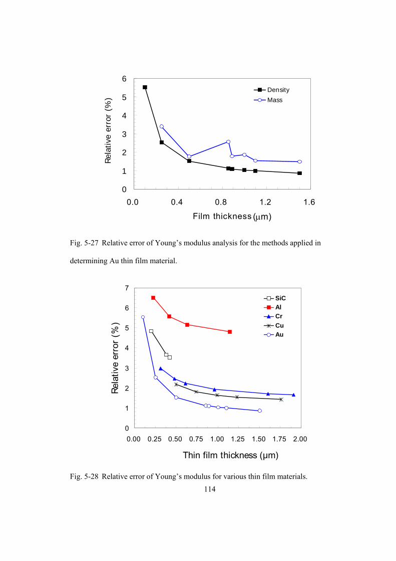
114
0
1
2
3
4
5
6
0.0 0.4 0.8 1.2 1.6
Film thickness
Rel
ativ
e er
ror
(%)
Density
Mass
(µm)
Fig. 5-27 Relative error of Young’s modulus analysis for the methods applied in
determining Au thin film material.
(µm)
0
1
2
3
4
5
6
7
0.00 0.25 0.50 0.75 1.00 1.25 1.50 1.75 2.00
Thin film thickness
Rel
ativ
e er
ror (
%)
SiCAlCrCuAu
Thin film thickness (μm)
Rela
tive
erro
r (%
)
Fig. 5-28 Relative error of Young’s modulus for various thin film materials.
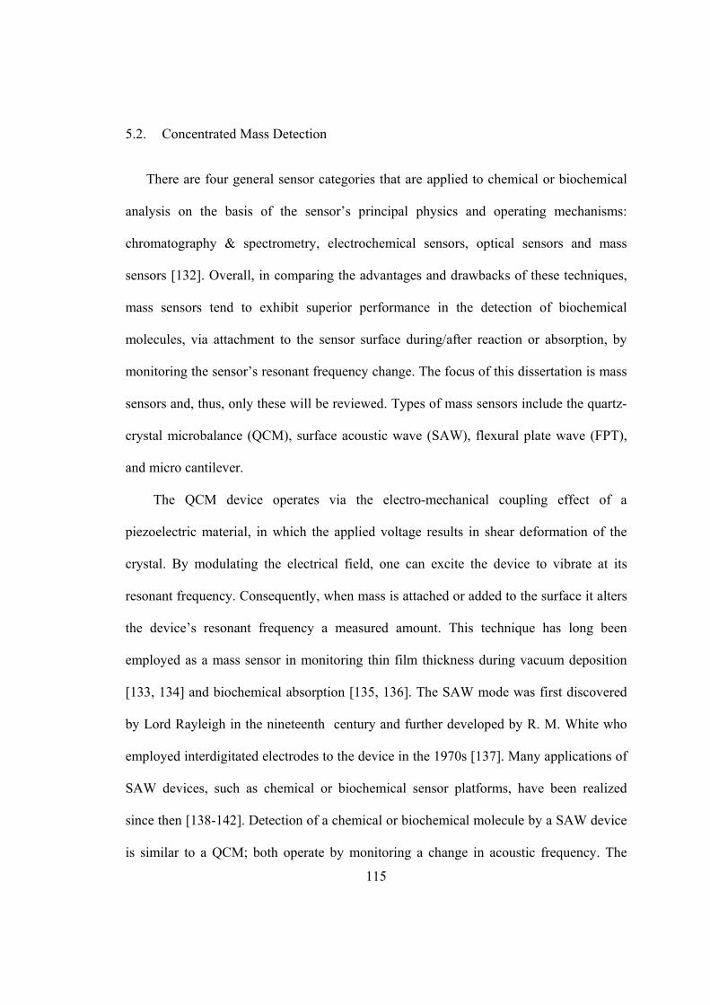
115
5.2. Concentrated Mass Detection
There are four general sensor categories that are applied to chemical or biochemical
analysis on the basis of the sensor’s principal physics and operating mechanisms:
chromatography & spectrometry, electrochemical sensors, optical sensors and mass
sensors [132]. Overall, in comparing the advantages and drawbacks of these techniques,
mass sensors tend to exhibit superior performance in the detection of biochemical
molecules, via attachment to the sensor surface during/after reaction or absorption, by
monitoring the sensor’s resonant frequency change. The focus of this dissertation is mass
sensors and, thus, only these will be reviewed. Types of mass sensors include the quartz-
crystal microbalance (QCM), surface acoustic wave (SAW), flexural plate wave (FPT),
and micro cantilever.
The QCM device operates via the electro-mechanical coupling effect of a
piezoelectric material, in which the applied voltage results in shear deformation of the
crystal. By modulating the electrical field, one can excite the device to vibrate at its
resonant frequency. Consequently, when mass is attached or added to the surface it alters
the device’s resonant frequency a measured amount. This technique has long been
employed as a mass sensor in monitoring thin film thickness during vacuum deposition
[133, 134] and biochemical absorption [135, 136]. The SAW mode was first discovered
by Lord Rayleigh in the nineteenth century and further developed by R. M. White who
employed interdigitated electrodes to the device in the 1970s [137]. Many applications of
SAW devices, such as chemical or biochemical sensor platforms, have been realized
since then [138-142]. Detection of a chemical or biochemical molecule by a SAW device
is similar to a QCM; both operate by monitoring a change in acoustic frequency. The
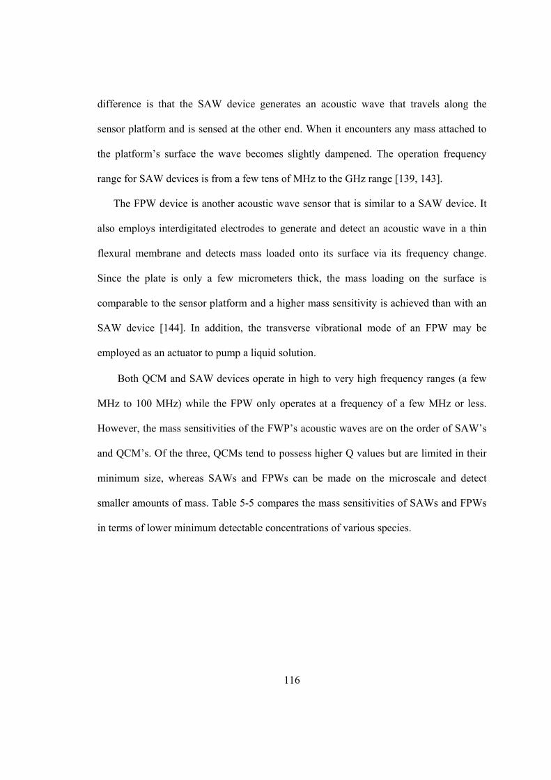
116
difference is that the SAW device generates an acoustic wave that travels along the
sensor platform and is sensed at the other end. When it encounters any mass attached to
the platform’s surface the wave becomes slightly dampened. The operation frequency
range for SAW devices is from a few tens of MHz to the GHz range [139, 143].
The FPW device is another acoustic wave sensor that is similar to a SAW device. It
also employs interdigitated electrodes to generate and detect an acoustic wave in a thin
flexural membrane and detects mass loaded onto its surface via its frequency change.
Since the plate is only a few micrometers thick, the mass loading on the surface is
comparable to the sensor platform and a higher mass sensitivity is achieved than with an
SAW device [144]. In addition, the transverse vibrational mode of an FPW may be
employed as an actuator to pump a liquid solution.
Both QCM and SAW devices operate in high to very high frequency ranges (a few
MHz to 100 MHz) while the FPW only operates at a frequency of a few MHz or less.
However, the mass sensitivities of the FWP’s acoustic waves are on the order of SAW’s
and QCM’s. Of the three, QCMs tend to possess higher Q values but are limited in their
minimum size, whereas SAWs and FPWs can be made on the microscale and detect
smaller amounts of mass. Table 5-5 compares the mass sensitivities of SAWs and FPWs
in terms of lower minimum detectable concentrations of various species.
117
Table 5-5 Minimal detectable concentration for SAW and FPW [144].
>10,0002500535SAW
2508075FPW
Helium(ppm)
Nitrous(ppm)
Methanol(ppm)
Devices
Cantilever-based chemical and biochemical sensors have been studied for the past
decade or so [36, 83, 145-156]. Two important developments in the area include:
Cleveland et al. determined the spring constant of a cantilever by measuring the
resonance frequency change due to mass added on the tip [83] and Gimzewski et al. [147]
observed that chemical reactions taking place on the cantilever can be monitored via its
deflection [147]. In 1995, Chen and Thundat [36, 38] demonstrated that cantilever
resonant frequency shift was associated with the surface absorption of mass or molecules.
Since then many researchers have explored the application of cantilever sensors in
widespread areas for detection of chemical or biological agents [157]. Such detection is
based either on the measurement of cantilever deflection [37, 46, 147, 158, 159] or on
the resonant frequency shift [36, 153, 154, 160]. A very high mass sensitivity of 0.32
pg/Hz was reported by Sone [161] for the cantilever-based sensors.
By comparing the various types of mass sensors described above with their mass
sensitivity and minimal detectable mass density in Table 5-6 reveals that the cantilever
and FPW mass sensors both possess a similar order of detection level. However, Sone
[161] reported that a mass sensitivity of 0.32 pg/Hz can be obtained, which inspired
researchers to continue to work on cantilever sensors as an alternative technology.
118
Table 5-6 Comparison of mass sensors.
Techniques Operation
frequency (MHz)Sm Sm (cm2/g) MDMD Reference
GCMS NA NA ~1 pg ~1 pg [162]
QCM 6 tρ
1∝ 14 10 ng/cm2 [163]
SAW 112 ρλ1
∝ 151 1.2 ng/cm2 [163]
FPW 2.6 tρ
1∝ 951 0.4 ng/cm2 [163]
Cantilever 5~0.005 tρ
1∝ 991~1363 0.67 ng/cm2 [163]
Since 1998, Grimes’ research group [164, 165] has been working on magnetoelastic
materials, primarily Metglas strip, as a chemical sensor platform that is operated in the
longitudinal vibration mode. Based on the resonant frequency change, the sum of mass
(aggregated chemical molecules) absorbed on the sensor surface can be determined.
Since then, numerous applications have been explored by Grimes’ group including
measurement of pressure, temperature, liquid viscosity, humidity, and fluid-flow velocity
as well as environmental monitoring [54, 166-175]; pH value sensing [173, 176-178];
hydrogen, ammonia and other gas detection [18, 57, 179-181]; thin film Young’s
modulus measurement [32]; biomass/biomolecule detection [17, 53, 56, 182, 183]; and
chemical reactions [184, 185]. An illuminating review of those applications can be found
in the literature [13]. In recent years, Auburn University’s Detection and Food Safety
119
Center (AUDFS) has dedicated much research effort by a similar principle, mainly based
on freestanding beams and particles.
The most common method of binding biomolecule cells onto the sensor surface for
mass detection is using a specific receptor recognizing only the agent of interest, which
then, binds the antigen or spores to the sensor. As discussed above, the resonant
frequency changes as a result of this process. The receptors employed by AUDFS in
magnetostrictive sensors include antibodies and phage, more details of which can be
found in [16, 20, 21]. These references describe sensors constructed of Metglas. These
writings demonstrate it as a material of choice in detecting biological species. However,
these works only deal with the mass evenly distributed on the sensor’s surface; almost no
one addresses unevenly distributed mass on a sensor, especially when the sensor vibrates
in the longitudinal mode. In the following, details of measuring the concentrated mass
attached to the sensor’s surface are reported.
5.2.1. Experimental Details
With consideration for the convenience of the test setup, the free-free ended beam
was selected as the sensor platform for investigating the resonant frequency change due
to a concentrated mass attachment. Sensors with dimensions of 5 mm length and 1 mm
width were cut from a 28 µm thick Metglas 2826 MB strip. These specimens were
prepared, by cleaning and drying, using the identical procedures described before. Glass
beads [186] with a diameter about 425 µm were used to simulate the concentrated mass
and were carefully loaded on to the sensor surface at different locations and secured with
120
glue. The average mass of a sensor and glass bead are 1066 µg and 181.5 µg, respectively.
It should be noted that these experiments are aimed as assessing the position of the mass
concentrations and not focused on demonstrating minimum sensitivity. Thus, significant
sized beads were employed. The amount of glue employed for each bead was controlled
to the best of our ability to minimize its influence. After a glass bead was loaded on the
sensor surface, it was immobilized by drying at room temperature for at least two hours.
The glass beads were randomly loaded onto the sensor surface, but their locations were
characterized and reorganized afterwards. The resonant frequency of the sensor was
measured before and after attachment of the glass bead in a manner identical to which is
discussed in section 2.
5.2.2. Results and Discussion
Fig. 5-29 shows electron microscopic images of the glass beads attached to the
sensors at various locations. In all cases, the measured resonant frequency of a free-free
ended sensor with glass bead attached at different locations decreased relative to the
frequency before attachment. Table 5-7 lists these results giving resonant frequencies
before (f0) and after (f) bead attachment. Note that x denotes the position for a single bead
and x1 and x2 the positions when two beads were attached. Fig. 5-30 shows the recorded
frequency spectrum for test case #2 where the glass bead was attached to the center of the
sensor surface, with the neutral position in longitudinal direction; but slightly off-central
line. No significant resonant frequency shift was observed for this position. As the bead
was moved away from the neutral point towards the free ends the frequency shift
increased. The shift reached a maximum when the glass bead was loaded at a position
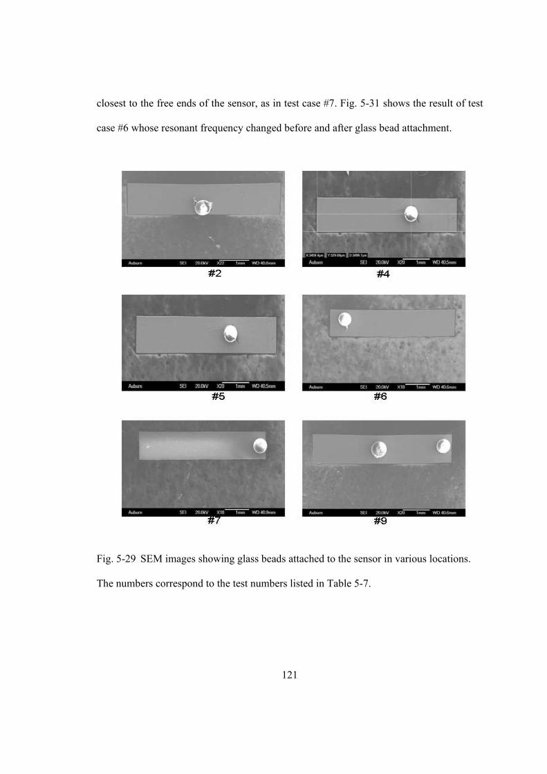
121
closest to the free ends of the sensor, as in test case #7. Fig. 5-31 shows the result of test
case #6 whose resonant frequency changed before and after glass bead attachment.
Fig. 5-29 SEM images showing glass beads attached to the sensor in various locations.
The numbers correspond to the test numbers listed in Table 5-7.
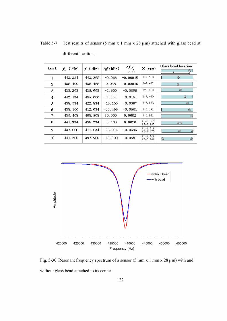
122
Table 5-7 Test results of sensor (5 mm x 1 mm x 28 µm) attached with glass bead at
different locations.
420000 425000 430000 435000 440000 445000 450000 455000Frequency (Hz)
Ampl
itude
without beadwith bead
Fig. 5-30 Resonant frequency spectrum of a sensor (5 mm x 1 mm x 28 µm) with and
without glass bead attached to its center.
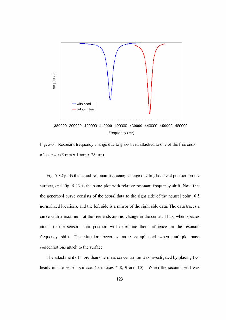
123
380000 390000 400000 410000 420000 430000 440000 450000 460000
Frequency (Hz)
Ampl
itude
with beadwithout bead
Fig. 5-31 Resonant frequency change due to glass bead attached to one of the free ends
of a sensor (5 mm x 1 mm x 28 µm).
Fig. 5-32 plots the actual resonant frequency change due to glass bead position on the
surface, and Fig. 5-33 is the same plot with relative resonant frequency shift. Note that
the generated curve consists of the actual data to the right side of the neutral point, 0.5
normalized locations, and the left side is a mirror of the right side data. The data traces a
curve with a maximum at the free ends and no change in the center. Thus, when species
attach to the sensor, their position will determine their influence on the resonant
frequency shift. The situation becomes more complicated when multiple mass
concentrations attach to the surface.
The attachment of more than one mass concentration was investigated by placing two
beads on the sensor surface, (test cases # 8, 9 and 10). When the second bead was
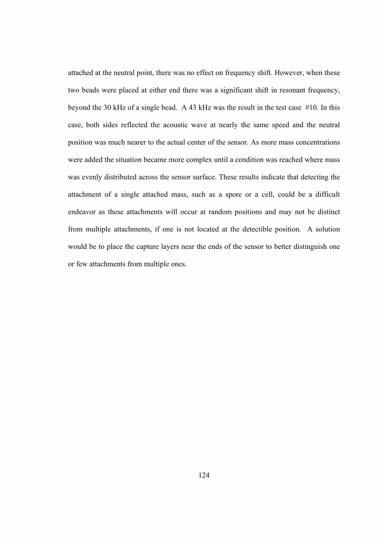
124
attached at the neutral point, there was no effect on frequency shift. However, when these
two beads were placed at either end there was a significant shift in resonant frequency,
beyond the 30 kHz of a single bead. A 43 kHz was the result in the test case #10. In this
case, both sides reflected the acoustic wave at nearly the same speed and the neutral
position was much nearer to the actual center of the sensor. As more mass concentrations
were added the situation became more complex until a condition was reached where mass
was evenly distributed across the sensor surface. These results indicate that detecting the
attachment of a single attached mass, such as a spore or a cell, could be a difficult
endeavor as these attachments will occur at random positions and may not be distinct
from multiple attachments, if one is not located at the detectible position. A solution
would be to place the capture layers near the ends of the sensor to better distinguish one
or few attachments from multiple ones.
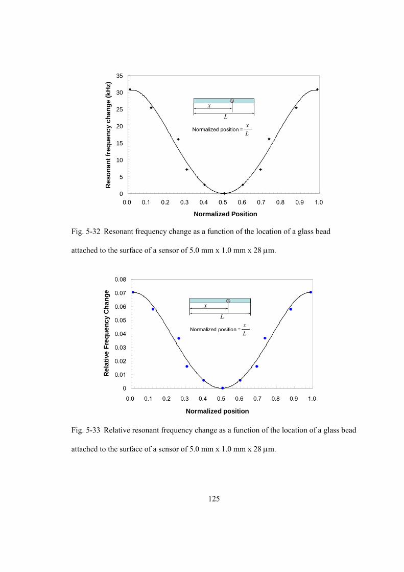
125
0
5
10
15
20
25
30
35
0.0 0.1 0.2 0.3 0.4 0.5 0.6 0.7 0.8 0.9 1.0
Normalized loaction
Res
onan
t fre
quen
cy c
hnag
e (k
Hz)
x
L
Lx
Normalized position =
Normalized Position
Res
onan
t fre
quen
cy c
hang
e (k
Hz)
Fig. 5-32 Resonant frequency change as a function of the location of a glass bead
attached to the surface of a sensor of 5.0 mm x 1.0 mm x 28 µm.
0
0.01
0.02
0.03
0.04
0.05
0.06
0.07
0.08
0.0 0.1 0.2 0.3 0.4 0.5 0.6 0.7 0.8 0.9 1.0
Nomarlized position
Rel
ativ
e fr
eque
ncy
chan
ge
x
L
Lx
Normalized position =
Normalized position
Rel
ativ
e Fr
eque
ncy
Cha
nge
Fig. 5-33 Relative resonant frequency change as a function of the location of a glass bead
attached to the surface of a sensor of 5.0 mm x 1.0 mm x 28 µm.
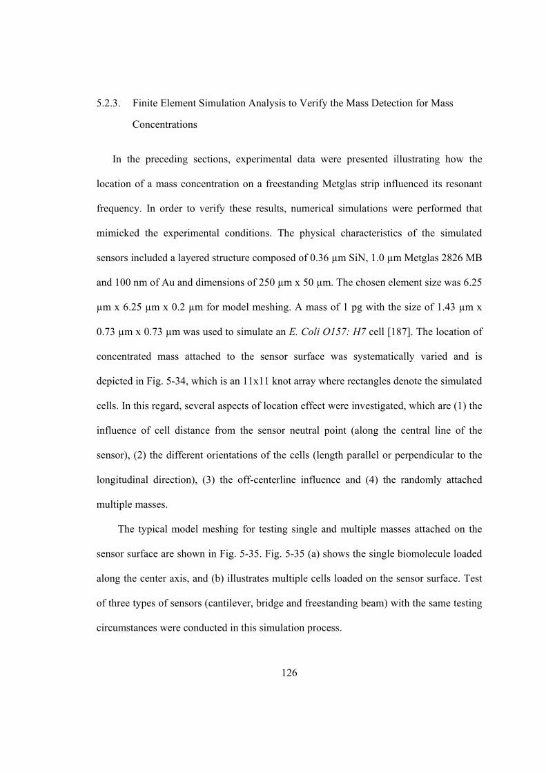
126
5.2.3. Finite Element Simulation Analysis to Verify the Mass Detection for Mass
Concentrations
In the preceding sections, experimental data were presented illustrating how the
location of a mass concentration on a freestanding Metglas strip influenced its resonant
frequency. In order to verify these results, numerical simulations were performed that
mimicked the experimental conditions. The physical characteristics of the simulated
sensors included a layered structure composed of 0.36 µm SiN, 1.0 µm Metglas 2826 MB
and 100 nm of Au and dimensions of 250 µm x 50 µm. The chosen element size was 6.25
µm x 6.25 µm x 0.2 µm for model meshing. A mass of 1 pg with the size of 1.43 µm x
0.73 µm x 0.73 µm was used to simulate an E. Coli O157: H7 cell [187]. The location of
concentrated mass attached to the sensor surface was systematically varied and is
depicted in Fig. 5-34, which is an 11x11 knot array where rectangles denote the simulated
cells. In this regard, several aspects of location effect were investigated, which are (1) the
influence of cell distance from the sensor neutral point (along the central line of the
sensor), (2) the different orientations of the cells (length parallel or perpendicular to the
longitudinal direction), (3) the off-centerline influence and (4) the randomly attached
multiple masses.
The typical model meshing for testing single and multiple masses attached on the
sensor surface are shown in Fig. 5-35. Fig. 5-35 (a) shows the single biomolecule loaded
along the center axis, and (b) illustrates multiple cells loaded on the sensor surface. Test
of three types of sensors (cantilever, bridge and freestanding beam) with the same testing
circumstances were conducted in this simulation process.
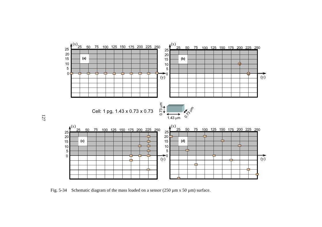
127
Fig. 5-34 Schematic diagram of the mass loaded on a sensor (250 µm x 50 µm) surface.
05
10152025 25 50 75 100 125 225175 200150 250
(y)
(x)
05
10152025
25 50 75 100 125 225175 200150 250
(y)
(x)
05
10152025 25 50 75 100 125 225175 200150 250
(y)
(x)
1.43 µm 0.73 µ
m
0.73
µm
Cell: 1 pg, 1.43 x 0.73 x 0.73
05
10152025 25 50 75 100 125 225175 200150 250
(y)
(x)
(a) (b)
(c) (d)
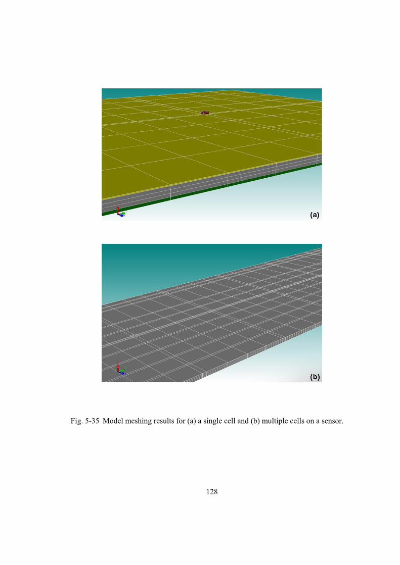
128
Fig. 5-35 Model meshing results for (a) a single cell and (b) multiple cells on a sensor.
129
5.2.3.1. Results of Resonant Frequency Change Due to a Single Cell Attachment
A simulated single E. Coli O157:H17 cell was attached to the sensor surface at the
central line (along the y axis) at different locations with the same orientation as shown in
Fig. 5-34 (a). The resonant frequency shifts of the first resonant state (sensitivity in this
case for the mass is a unit) for a single bacterium mass with its location along the
longitudinal direction are shown in Fig. 5-36 for sensors made in cantilever, bridge and
beam configurations. It is clear that in all three cases the frequency change for a
concentrated mass is a function of the location along the central axis. These results agree
with experimental findings on the freestanding beams shown in Fig. 5-32. When these
structures resonate in their first mode, the deformation is different depending on location
as discussed in section 2. Here, the largest deformation occurs at the free ends for a
cantilever or freestanding beam, while the largest deformation occurs at the center point
of a fix-fix ended bridge, and no deformation occurs at the fixed ends of a cantilever or
bridge and the middle of a freestanding beam. The positions of maximum deformation on
each structure correspond exactly to the largest frequency shift in each case. The ability,
then, to detect the attachment of a single cell will depend on whether it attaches to the
areas where deformation occurs during resonance. For example, the largest frequency
change on a cantilever of dimensions used in the simulations can be as high as 42.5Hz at
the tip of the free end area but is close to zero if the mass is located near the fixed end. At
the center of the cantilever, almost half of the largest change in value, about 21 Hz is
possible. Only when the mass location is 125µm or further away from the fixed end, can
the sensitivity reach the criteria for detecting a single bacterium as discussed in section
3.2. The average frequency shift is 21.3 Hz for the eleven positions investigated in the
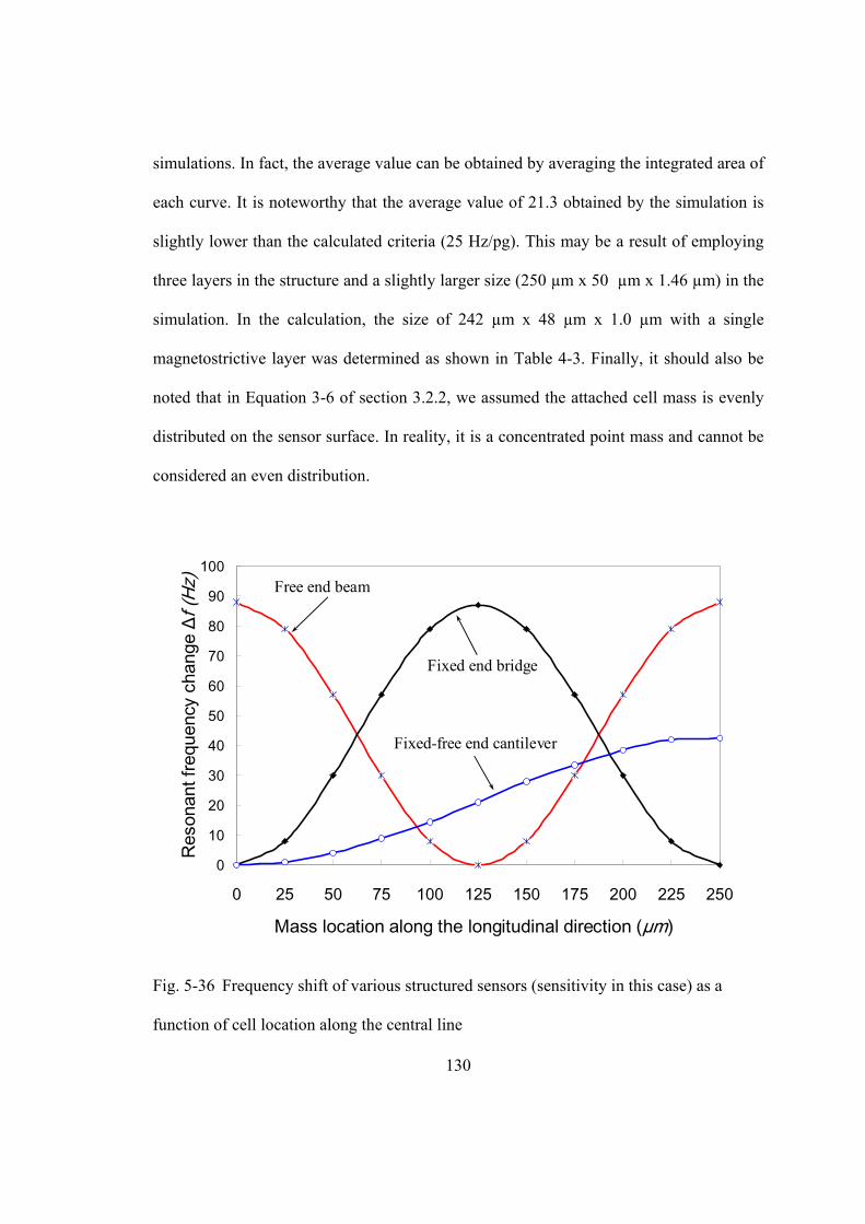
130
simulations. In fact, the average value can be obtained by averaging the integrated area of
each curve. It is noteworthy that the average value of 21.3 obtained by the simulation is
slightly lower than the calculated criteria (25 Hz/pg). This may be a result of employing
three layers in the structure and a slightly larger size (250 µm x 50 µm x 1.46 µm) in the
simulation. In the calculation, the size of 242 µm x 48 µm x 1.0 µm with a single
magnetostrictive layer was determined as shown in Table 4-3. Finally, it should also be
noted that in Equation 3-6 of section 3.2.2, we assumed the attached cell mass is evenly
distributed on the sensor surface. In reality, it is a concentrated point mass and cannot be
considered an even distribution.
0
10
20
30
40
50
60
70
80
90
100
0 25 50 75 100 125 150 175 200 225 250
Mass location along the longitudinal direction (µm)
Res
onan
t fre
quen
cy c
hang
e Δf
(Hz) Free end beam
Fixed end bridge
Fixed-free end cantilever
Fig. 5-36 Frequency shift of various structured sensors (sensitivity in this case) as a
function of cell location along the central line
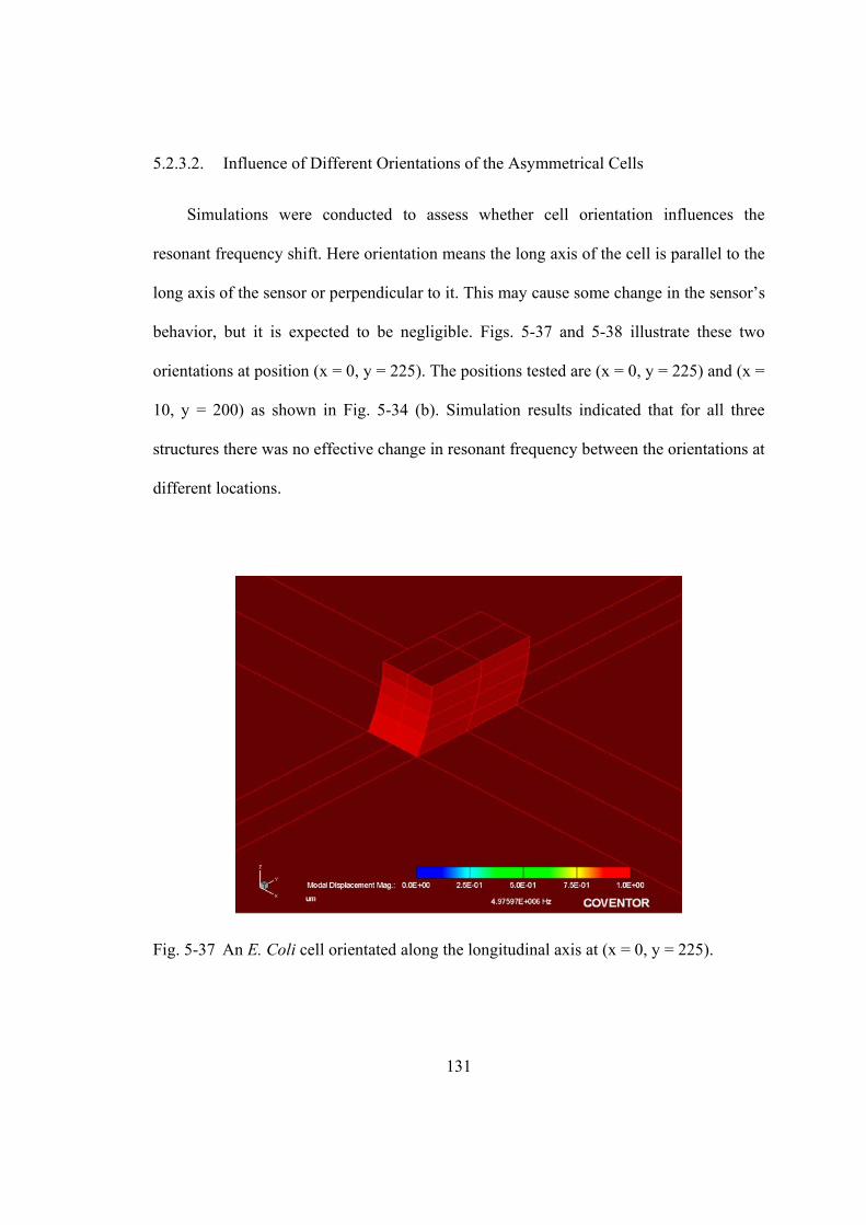
131
5.2.3.2. Influence of Different Orientations of the Asymmetrical Cells
Simulations were conducted to assess whether cell orientation influences the
resonant frequency shift. Here orientation means the long axis of the cell is parallel to the
long axis of the sensor or perpendicular to it. This may cause some change in the sensor’s
behavior, but it is expected to be negligible. Figs. 5-37 and 5-38 illustrate these two
orientations at position (x = 0, y = 225). The positions tested are (x = 0, y = 225) and (x =
10, y = 200) as shown in Fig. 5-34 (b). Simulation results indicated that for all three
structures there was no effective change in resonant frequency between the orientations at
different locations.
Fig. 5-37 An E. Coli cell orientated along the longitudinal axis at (x = 0, y = 225).
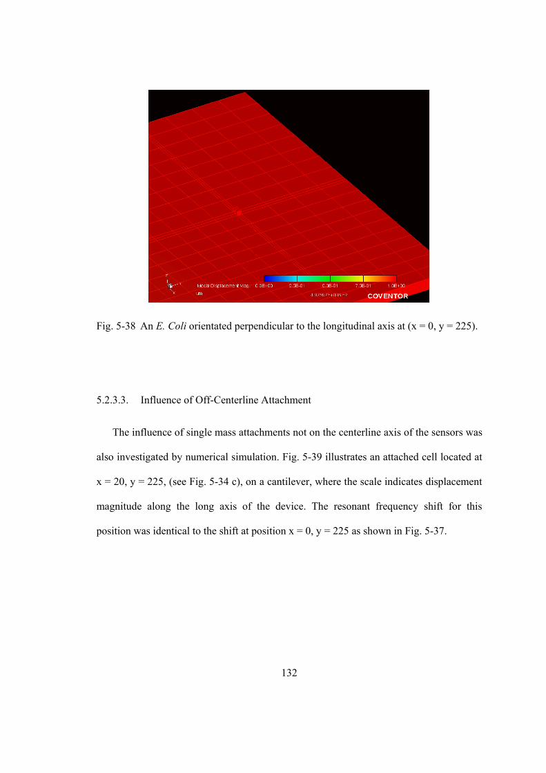
132
Fig. 5-38 An E. Coli orientated perpendicular to the longitudinal axis at (x = 0, y = 225).
5.2.3.3. Influence of Off-Centerline Attachment
The influence of single mass attachments not on the centerline axis of the sensors was
also investigated by numerical simulation. Fig. 5-39 illustrates an attached cell located at
x = 20, y = 225, (see Fig. 5-34 c), on a cantilever, where the scale indicates displacement
magnitude along the long axis of the device. The resonant frequency shift for this
position was identical to the shift at position x = 0, y = 225 as shown in Fig. 5-37.
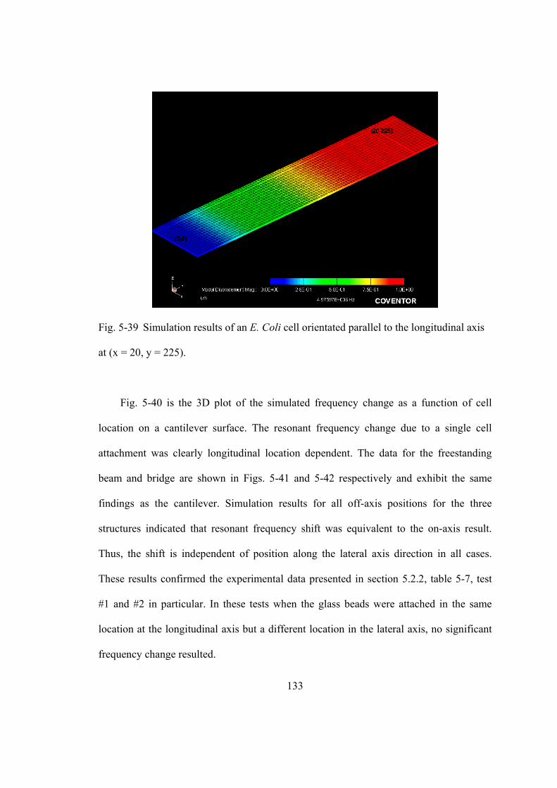
133
Fig. 5-39 Simulation results of an E. Coli cell orientated parallel to the longitudinal axis
at (x = 20, y = 225).
Fig. 5-40 is the 3D plot of the simulated frequency change as a function of cell
location on a cantilever surface. The resonant frequency change due to a single cell
attachment was clearly longitudinal location dependent. The data for the freestanding
beam and bridge are shown in Figs. 5-41 and 5-42 respectively and exhibit the same
findings as the cantilever. Simulation results for all off-axis positions for the three
structures indicated that resonant frequency shift was equivalent to the on-axis result.
Thus, the shift is independent of position along the lateral axis direction in all cases.
These results confirmed the experimental data presented in section 5.2.2, table 5-7, test
#1 and #2 in particular. In these tests when the glass beads were attached in the same
location at the longitudinal axis but a different location in the lateral axis, no significant
frequency change resulted.
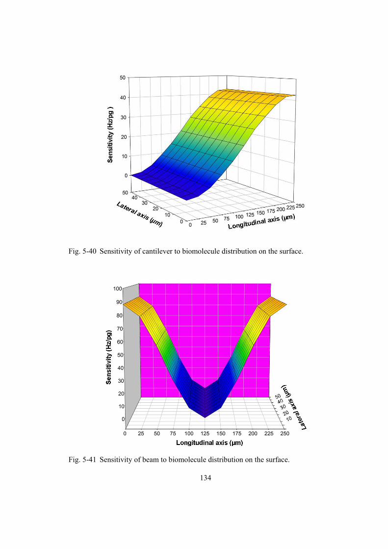
134
Fig. 5-40 Sensitivity of cantilever to biomolecule distribution on the surface.
Fig. 5-41 Sensitivity of beam to biomolecule distribution on the surface.
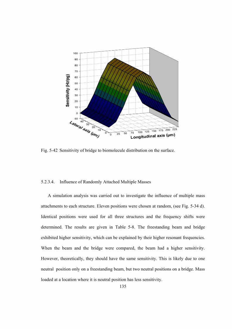
135
Fig. 5-42 Sensitivity of bridge to biomolecule distribution on the surface.
5.2.3.4. Influence of Randomly Attached Multiple Masses
A simulation analysis was carried out to investigate the influence of multiple mass
attachments to each structure. Eleven positions were chosen at random, (see Fig. 5-34 d).
Identical positions were used for all three structures and the frequency shifts were
determined. The results are given in Table 5-8. The freestanding beam and bridge
exhibited higher sensitivity, which can be explained by their higher resonant frequencies.
When the beam and the bridge were compared, the beam had a higher sensitivity.
However, theoretically, they should have the same sensitivity. This is likely due to one
neutral position only on a freestanding beam, but two neutral positions on a bridge. Mass
loaded at a location where it is neutral position has less sensitivity.
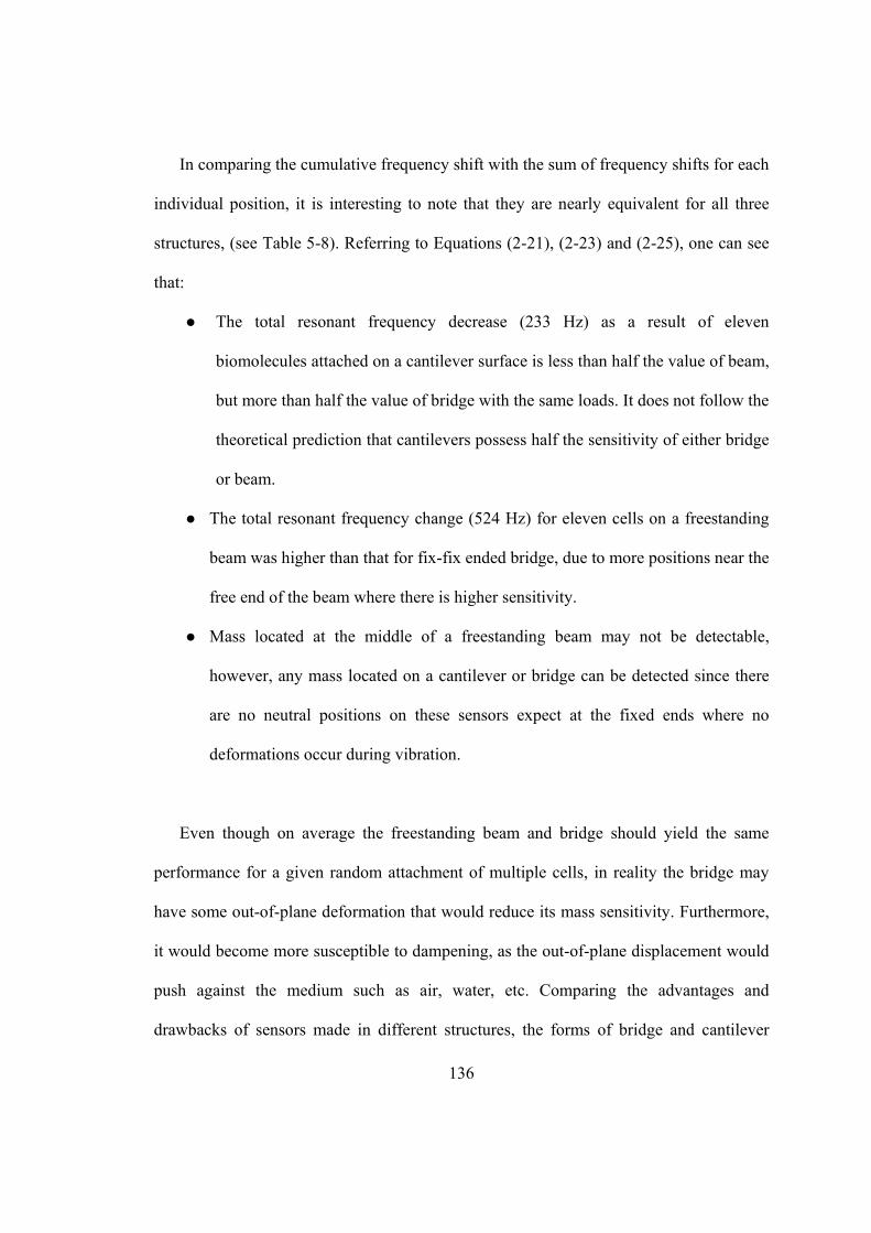
136
In comparing the cumulative frequency shift with the sum of frequency shifts for each
individual position, it is interesting to note that they are nearly equivalent for all three
structures, (see Table 5-8). Referring to Equations (2-21), (2-23) and (2-25), one can see
that:
The total resonant frequency decrease (233 Hz) as a result of eleven
biomolecules attached on a cantilever surface is less than half the value of beam,
but more than half the value of bridge with the same loads. It does not follow the
theoretical prediction that cantilevers possess half the sensitivity of either bridge
or beam.
The total resonant frequency change (524 Hz) for eleven cells on a freestanding
beam was higher than that for fix-fix ended bridge, due to more positions near the
free end of the beam where there is higher sensitivity.
Mass located at the middle of a freestanding beam may not be detectable,
however, any mass located on a cantilever or bridge can be detected since there
are no neutral positions on these sensors expect at the fixed ends where no
deformations occur during vibration.
Even though on average the freestanding beam and bridge should yield the same
performance for a given random attachment of multiple cells, in reality the bridge may
have some out-of-plane deformation that would reduce its mass sensitivity. Furthermore,
it would become more susceptible to dampening, as the out-of-plane displacement would
push against the medium such as air, water, etc. Comparing the advantages and
drawbacks of sensors made in different structures, the forms of bridge and cantilever
137
show that they are the preferred structure for detection of biological cell. Not only they
can detect a mass anywhere on the surface, but they can also be integrated into a chip that
can greatly reduce the problem of handling the device for end users.
Table 5-8 Summary of simulation results of frequency changes and sensitivities for the
three types of sensors in response to E Coli O157 cells bonded onto a (250 µm x 5 µm x
5 µm) sensor’s surface
5.3. Summary
The benefit of using a magnetostrictive sensor to measure the thin film Young’s
modulus was demonstrated. Such a technique offers a cost-effective, user-friendly and
non-destructive test of thin film properties. The improved methodology of determining
thin film Young’s modulus by assuming film density being equivalent to bulk density
significantly reduced the amount of error associated with the measurement.
Magnetostrictive sensors respond differently to different thin film materials, and the
138
response depends on the combination of relative density and relative modulus change for
the sensor and film composite. The same follows for the Q-factor.
The Young’s modulus of Au film determined through the different methods, e.g.
measuring the mass and assumed film density, is rather close each other. The results
were also confirmed using the MDE technique. In addition, both simulation and
experimentation determined the Au and Cu films’ moduli are in good agreement. This
longitudinal vibration mode technique showed less relative error than the transverse
vibration mode for determining the thin film elastic modulus.
Glass beads were employed to simulate the attachment of a concentrated mass on
sensors that were constructed as freestanding beams. For single bead attachments, the
largest change was observed when the concentrated mass was loaded at the free end of
the sensor, while no change in the resonant frequency occurred when it was attached to
the middle of the sensor (x = L/2), the natural position of the free-free ended beam. The
bead position was mapped out as a function of position on the sensor surface.
Additionally, the influence of multiple mass concentrations was found to shift the neutral
position of the beam due to different acoustic wave speeds on either side of the beam. It
was determined then that single mass attachments would be difficult to discern from
multiple one unless the capture areas were concentrated near the free ends of the beam.
Simulation results indicated that the sensor response to the attachment of a single
cell/spore is also dependent on the location of the mass along the longitudinal axis only,
but not the lateral axis. Cell orientation does not affect the sensors’ response or sensitivity.
The resonant frequency change for multiple biomolecules bonded on the sensor surface is
equivalent to the value of the sum of the frequency changes induced in each individual
139
case. In the simulation, the freestanding beam showed higher sensitivity than bridge-
structured sensors, but the mass located at the neutral position of a freestanding beam
sensor will not be detectable. This drawback does not apply to a cantilever- or a bridge-
structured sensor.
140
6. DEPOSITION OF MAGNETOSTRICTIVE THIN FILM MATERIAL AND
CHARACTERIZATION OF MICROFABRICATED MICROSCALE SENSORS
The operating principle of magnetostrictive sensors and their potential applications
in the detection of biological species has been discussed in the preceding sections. From
the results, it was clear that to improve the sensitivity for detecting very small quantities
of a species, it is essential to reduce the sensor’s mass (reduce its size relative to the
biological species) and to increase the sensor’s resonant frequency. To this end, it is
desirable to reduce the sensor’s size into the microscale size range. Thus, the sensors
must be constructed from thin films of magnetostrictive material. Depositing these thin
films as well as the microfabrication processes to machine them become critical factors in
the sensors’ performance. This section reports on investigating the optimum parameters
for sputter deposition of Metglas 2826 MB magnetostrictive thin films, their micro-
machining and corresponding characterization and testing as microscale sensors.
6.1. Magnetostrictive/Magnetoelastic Thin Films
Engineers and scientists have employed magnetic materials in data storage devices
for many years. Many applications of magnetic materials and their requirements can be
found in Table 6-1 [188]. This study focused on the soft
ferromagnetic materials with magnetostrictive properties that can be applied to
resonating sensor construction. Giant magnetostrictive materials such as TbFeCo [189]
141
constituted of rare earth elements (Tb, Sm, Dy) and transition elements (Fe, Ni, Co) have
large factors of magnetomechanical coupling. TbFe2 shows the largest positive and
SmFe2 the largest negative magnetostriction [190]. As an example, Tb-Fe-Co thin films
were studied for force measurement due to their large positive magnetostriction. Some
criteria must be taken into account, though, when applying magnetostrictive materials in
actuation and sensing devices such as mass sensors. These materials must have low
magnetic anisotropy properties, so that noticeable differential responses or significant
changes in strain as a result of a small change in the applied field can be obtained. In fact,
such strain changes result from the magnetization of magnetostrictive materials under an
applied external field. In addition, low to zero coercivity and remanence are essential to
ensure that the magnetization process is dominated by moment rotation (switching).
Giant magnetostrictive materials can be one of the candidates for mass sensor
applications. Fe-Co-Si-B based magnetostrictive thin films can be used as stress sensors
or high frequency RF devices [191, 192]. Other magnetic thin film materials including
TbDyFe, CoFe, TbFeB, FeNi, CoNiFe, FeBSiC and FeB, have been the subjects of
extensive research [193-201]. In most cases, a sputtering process is used for magnetic
thin film deposition because sputtering provides more flexible control and better film
quality. More information about thin film magnetostrictive materials deposition
techniques and their application can be found in the literature [202].
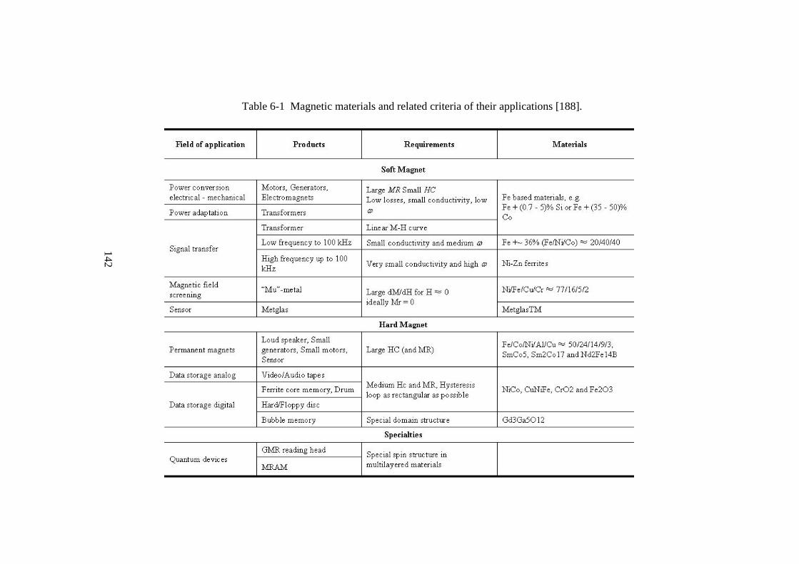
142
Table 6-1 Magnetic materials and related criteria of their applications [188].
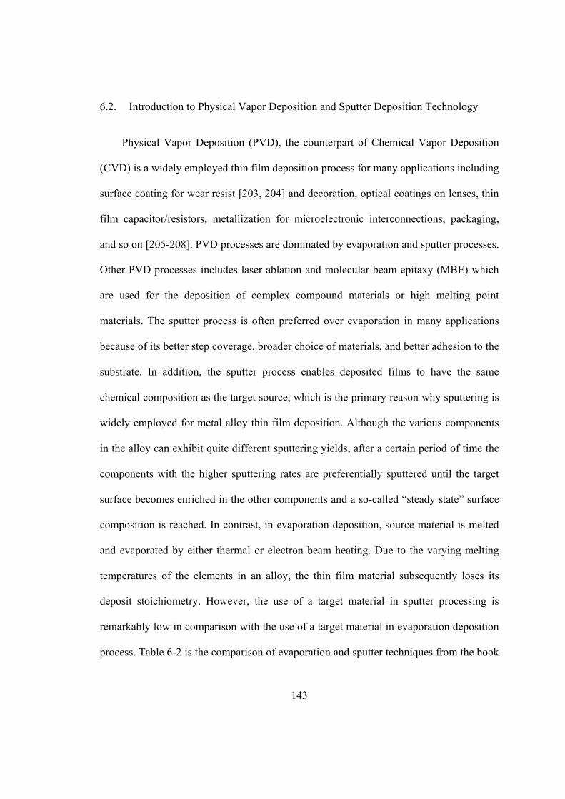
143
6.2. Introduction to Physical Vapor Deposition and Sputter Deposition Technology
Physical Vapor Deposition (PVD), the counterpart of Chemical Vapor Deposition
(CVD) is a widely employed thin film deposition process for many applications including
surface coating for wear resist [203, 204] and decoration, optical coatings on lenses, thin
film capacitor/resistors, metallization for microelectronic interconnections, packaging,
and so on [205-208]. PVD processes are dominated by evaporation and sputter processes.
Other PVD processes includes laser ablation and molecular beam epitaxy (MBE) which
are used for the deposition of complex compound materials or high melting point
materials. The sputter process is often preferred over evaporation in many applications
because of its better step coverage, broader choice of materials, and better adhesion to the
substrate. In addition, the sputter process enables deposited films to have the same
chemical composition as the target source, which is the primary reason why sputtering is
widely employed for metal alloy thin film deposition. Although the various components
in the alloy can exhibit quite different sputtering yields, after a certain period of time the
components with the higher sputtering rates are preferentially sputtered until the target
surface becomes enriched in the other components and a so-called “steady state” surface
composition is reached. In contrast, in evaporation deposition, source material is melted
and evaporated by either thermal or electron beam heating. Due to the varying melting
temperatures of the elements in an alloy, the thin film material subsequently loses its
deposit stoichiometry. However, the use of a target material in sputter processing is
remarkably low in comparison with the use of a target material in evaporation deposition
process. Table 6-2 is the comparison of evaporation and sputter techniques from the book
144
of “Fundamentals of Microfabrication-The Science and Miniaturization” [206], where
more details on the sputtering process in thin film deposition can be found.
Table 6-2 Comparison of evaporation and sputtering techniques [206].
Controlled by bias, pressure and substrate heatingDifficult to controlFilm properties (e.g. grain size, step coverage)
SmallLargeShadowing effect
ExcellentOften poorAdhesion
Several control possibleNot easy to controlThickness control
Many depositions can be carried out per targetOne deposition per chargeNumber of deposition
More expensiveLow costCapital equipment
Easy over large areaDifficultUniformity
GoodDifficultScaling up
LowHighDecomposition of material
ExpensiveEasyChange in source material
Radiation and particle damage is possibleOnly with e-beamX-ray damage
Alloy composition can be tightly controlledLittle or no controlAlloy composition stoichiometry
Easily done by sputtering etchNot an optionIn situ clean
Ionic bombardment damageVery low, with e-beam, x-ray damage possibleSurface damage
Unless magnetron is used substrate heating can be substantial Very lowSubstrate heating
Possibility of incorporating impurities (low to medium vacuum range)
Better (no gas inclusion, very high vacuum)Purity
Almost unlimitedlimitedChoice of materials
One atomic layer per secondThousand atomic layer per second (e.g. 0.5 µm for Al)Rate
SputteringEvaporation
145
During sputtering process, a high electrical potential is applied between two parallel
plates, ionization will take place if an inert gas (e.g. Ar) is introduced. The ionized Ar
(Ar+) is accelerated in the applied electrical field and gains high momentum energy.
When the energized Ar ions are shot onto the target surface, the atoms of the target
material are ejected from the target by bombardment and condensed onto the substrate, as
depicted in Fig. 6-1, causing a thin film to be deposited. In modern sputter systems, the
substrate can be plasma cleaned before the film deposition, which enhances the adhesion
of the film on the substrate. The film properties can be modified by applying bias or heat
during the deposition as well. High to ultra-high vacuum is often required for improved
film quality. To do so, a turbo molecular pump or turbo pump is commonly used to
replace the diffusion pump so that a better pumping efficiency and eradication of
contamination caused by back stream oil from the diffusion pump can be achieved.
To facilitate higher sputtering yields (eventually higher deposition rate), a magnetron
is implanted in the target electrode to confine the electron motion, hence stabilizing the
plasma. The magnetron sputter electrode usually consists of a permanent magnetic
material as shown in Fig. 6-2 (a & b). The magnetic field will restrict the electrons’
motion toward the target surface, so that the electrons will not move onto the target
surface or the chamber wall as a result of vanishing, which assures high plasma
concentration and high sputter yields. The disadvantage of the magnetron sputter
technique is that the efficiency of target usage is low.
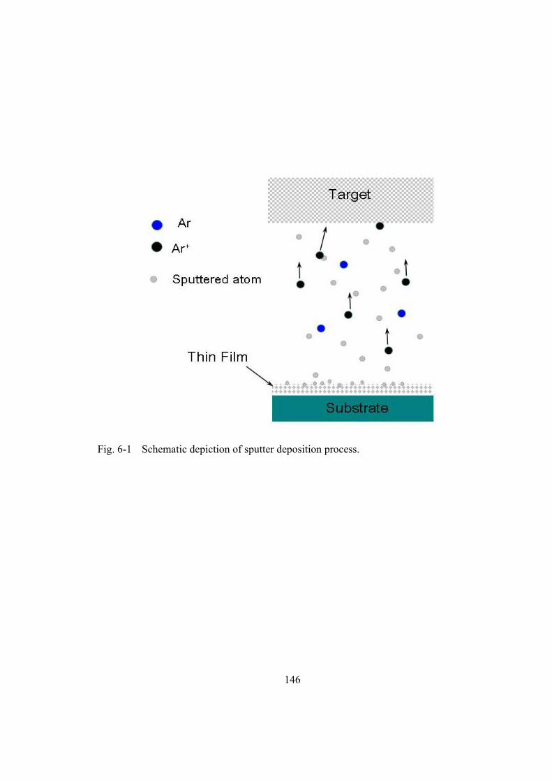
146
Fig. 6-1 Schematic depiction of sputter deposition process.
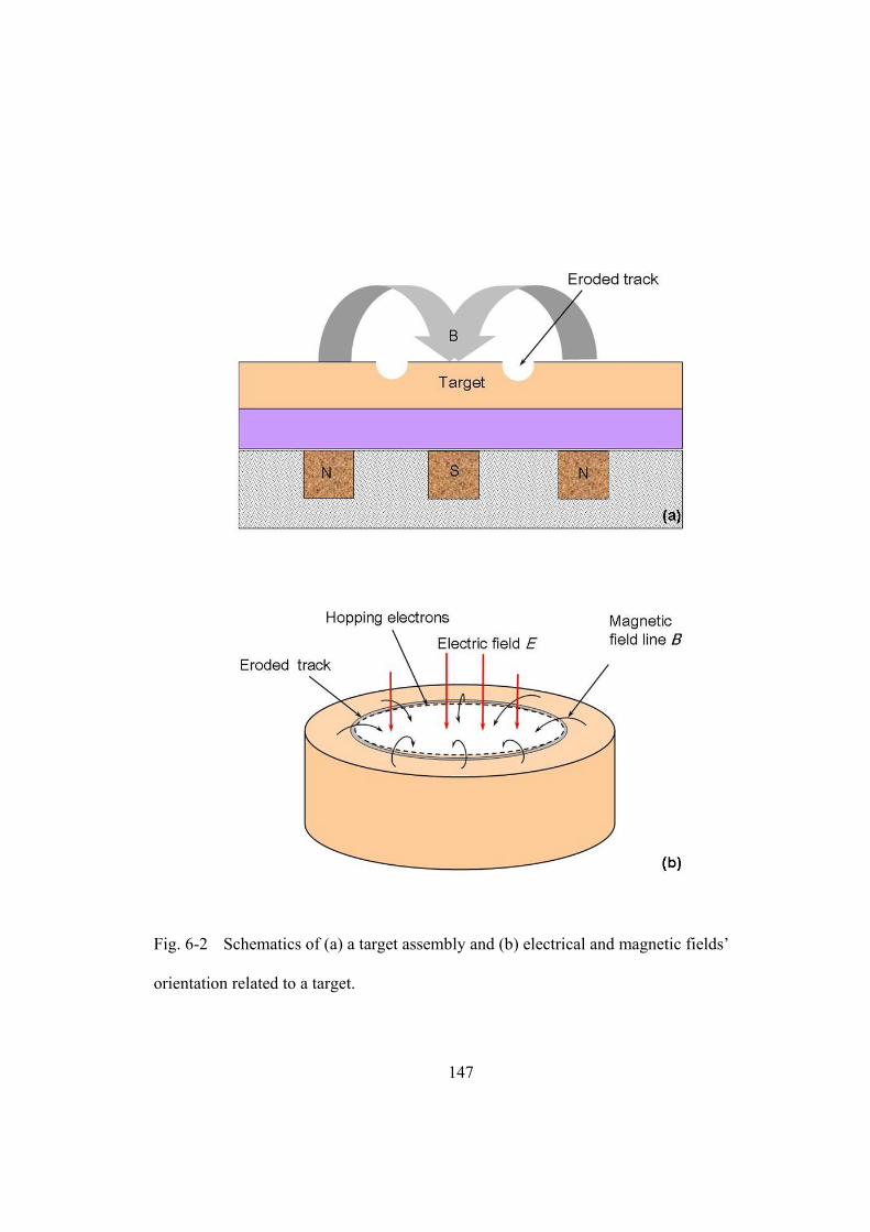
147
Fig. 6-2 Schematics of (a) a target assembly and (b) electrical and magnetic fields’
orientation related to a target.
148
In the case of sputtering magnetic materials, e.g. Ni, Fe, Co, and Metglas, the
magnetic field integrated in the cathode must be stronger than the one for general
nonmagnetic materials, in order to overcome the magnetic field effect of the target
materials. Previous studies of sputtering Metglas 2605 SC strip material showed the
facility of sputtering Metglas strip to form a thin film on a substrate [209].
In the sputtering deposition process, RF (radio frequency) and DC (direct current)
are the two options for power supply. RF power is generally used for non-conductive
targets, while DC is used for conductive target materials. RF power is delivered by a
capacitively coupling discharge process, in which the total ion and electron flow to the
target surface during an RF cycling must be zero. A negative self bias with respect to the
plasma potential thus develops. Since the mobility of an electron and an ion, e. g. Ar, is
different, a much larger current is drawn when the electrode is positive with respect to the
floating potential than when it is negative. In order to achieve net zero current, it is
essential to develop a DC bias so that the average potential is negative, as if there were a
negative DC connecting to the target (cathode). Therefore, the DC bias is a measure of
the RF sputter process. In the case of DC sputtering, as a DC is supplied to the target
(cathode), the plasma discharge process is simple. More details on RF and DC plasma
processes can be found in many books [210, 211].
Sputtering deposition is an intricate process, in which collisions occur between the
sputtered atoms, ionized sputtering ions, neutral Ar species, radicals and electrons.
Interactions take place between electrons, ions and radicals. The applied DC or RF power,
the vacuum pressure, substrate temperature and bias are important factors that may affect
the plasma discharge, sputter yield, and thin film properties. These parameters often
149
influence each other. For example, at higher vacuum pressure, many Ar molecules are
present resulting in more collisions (hence, shorter mean free path). The frequent
momentum transfer causes loss of energy of the Ar ion, which results in low sputter yield;
consequently, the deposition rate is low. Moreover, the sputtered atom will suffer from
many collisions that cause loss of the line-of-sight characteristic and energy as well. The
overall effects will produce a different property of thin film. The collision of electrons
also influences the electrical breakdown. The breakdown potential for a given sputter
system is a function of the product of pressure (p) and electrodes’ separation distance (d)
as described in the Paschen curve in Fig. 6-3 [210]. One can see if the applied electrical
potential is lower than the breakdown curve; under particular circumstances of pd value
the plasma will not ignite. The product of pressure p and distance d is a critical parameter
for the sputtering deposition process, and the minimum breakdown potential occurs at a
particular pd value.
A variety of sputtering deposition processes are possible, including co-sputtering and
reactive sputtering. Co-sputtering is a technique in which two or more target materials are
simultaneously sputtered to produce an alloy or mixture of multi component film. For
example, this process was used in deposition of the AuSn solder [212] and many others.
However, exact control of the composition is often difficult, especially deposition with
three and more elements such as Metglas 2826 MB that has four elements. This is not
only due to its complicated control but also to the lack of system capability. In this case,
direct sputtering from an alloyed target such as a Metglas strip to produce the similar
compositional film materials is the primary choice. Fig. 6-4 shows the system used in this
research (the plasma is on in the photo). Reactive sputtering deposition process is usually
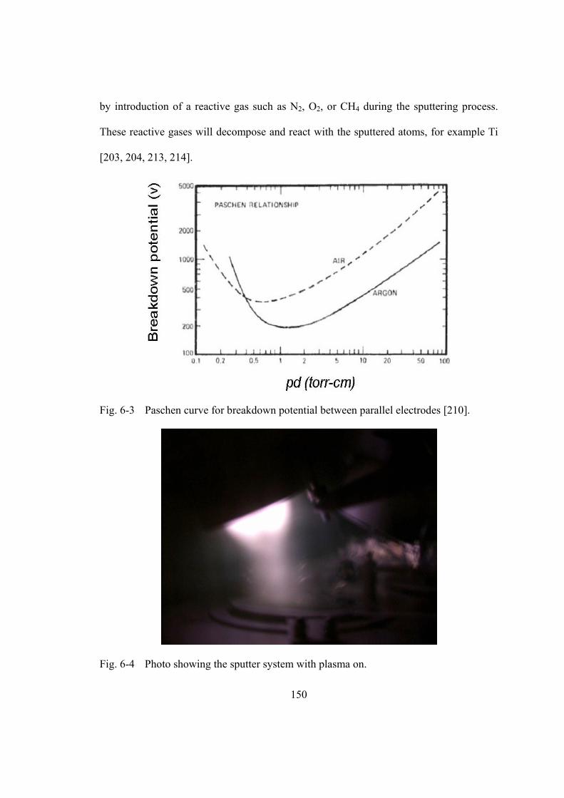
150
by introduction of a reactive gas such as N2, O2, or CH4 during the sputtering process.
These reactive gases will decompose and react with the sputtered atoms, for example Ti
[203, 204, 213, 214].
Fig. 6-3 Paschen curve for breakdown potential between parallel electrodes [210].
Fig. 6-4 Photo showing the sputter system with plasma on.
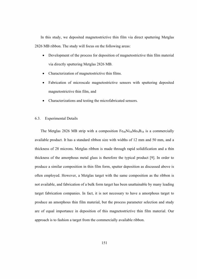
151
In this study, we deposited magnetostrictive thin film via direct sputtering Metglas
2826 MB ribbon. The study will focus on the following areas:
• Development of the process for deposition of magnetostrictive thin film material
via directly sputtering Metglas 2826 MB.
• Characterization of magnetostrictive thin films.
• Fabrication of microscale magnetostrictive sensors with sputtering deposited
magnetostrictive thin film, and
• Characterizations and testing the microfabricated sensors.
6.3. Experimental Details
The Metglas 2826 MB strip with a composition Fe40Ni38Mo4B18 is a commercially
available product. It has a standard ribbon size with widths of 12 mm and 50 mm, and a
thickness of 28 microns. Metglas ribbon is made through rapid solidification and a thin
thickness of the amorphous metal glass is therefore the typical product [9]. In order to
produce a similar composition in thin film form, sputter deposition as discussed above is
often employed. However, a Metglas target with the same composition as the ribbon is
not available, and fabrication of a bulk form target has been unattainable by many leading
target fabrication companies. In fact, it is not necessary to have a amorphous target to
produce an amorphous thin film material, but the process parameter selection and study
are of equal importance in deposition of this magnetostrictive thin film material. Our
approach is to fashion a target from the commercially available ribbon.
152
6.3.1. Fabrication of Sputtering Target
A sputter target requires good thermal and electrical conduction when it is mounted
onto the sputter cathode, including a Metglas sputter target. Solder, conductive silver
paste and conductive adhesives can all be used to bond a Metglas ribbon onto a Cu
backing plate. Conductive adhesive is the primary choice since the other two may
introduce an air gap between the Metglas ribbon and the backing plate. This improper
bonding may cause either poor electrical conduction or poor thermal conduction. The
resulting local overheating can burn the target material and shorten a target’s lifespan.
One may think that using multilayer Metglas ribbon bonded onto the backing plate will
make the target last longer. Capacitors, however, may develop between ribbons, and the
bonding material may alter composition. Furthermore, as ribbon layers are removed by
the energetic ions large pieces of the ribbon may fall and deposit onto the wafer. The
criteria for making a Metglas target, therefore, can be summarized as:
• Cu baking plate should be smooth and thin enough to assure good thermal and
electrical conducting,
• Bonding material should have high electrical and thermal conductivities plus
good adhesion,
• Single layer of ribbon should be used to avoid compositional and large particle
issues.
A 1.5 mm thick Cu backing plate was graded and polished to a near mirror finish,
cleaned, and dehydrated before bonding with the Metglas ribbon. The ribbon was cut to
the desired shape so as to completely cover the backing plate. The two were bonded
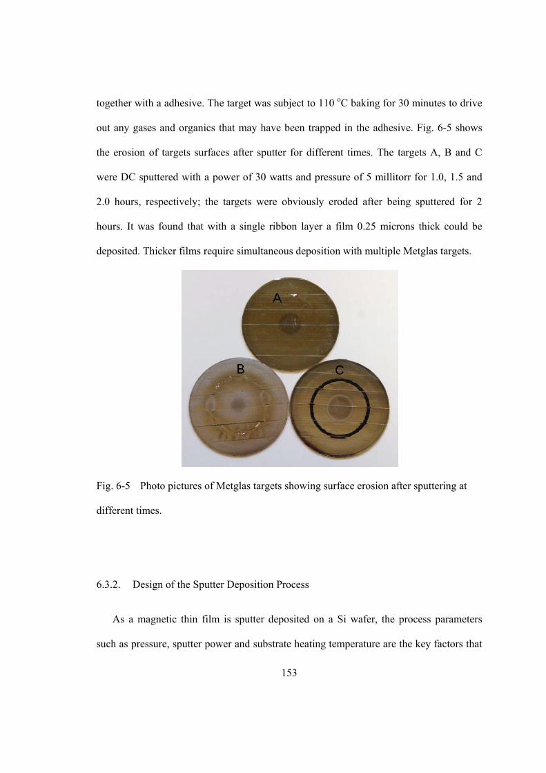
153
together with a adhesive. The target was subject to 110 oC baking for 30 minutes to drive
out any gases and organics that may have been trapped in the adhesive. Fig. 6-5 shows
the erosion of targets surfaces after sputter for different times. The targets A, B and C
were DC sputtered with a power of 30 watts and pressure of 5 millitorr for 1.0, 1.5 and
2.0 hours, respectively; the targets were obviously eroded after being sputtered for 2
hours. It was found that with a single ribbon layer a film 0.25 microns thick could be
deposited. Thicker films require simultaneous deposition with multiple Metglas targets.
Fig. 6-5 Photo pictures of Metglas targets showing surface erosion after sputtering at
different times.
6.3.2. Design of the Sputter Deposition Process
As a magnetic thin film is sputter deposited on a Si wafer, the process parameters
such as pressure, sputter power and substrate heating temperature are the key factors that
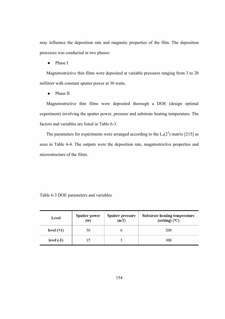
154
may influence the deposition rate and magnetic properties of the film. The deposition
processes was conducted in two phases:
Phase I
Magnetostrictive thin films were deposited at variable pressures ranging from 3 to 20
millitorr with constant sputter power at 30 watts.
Phase II
Magnetostrictive thin films were deposited thorough a DOE (design optimal
experiment) involving the sputter power, pressure and substrate heating temperature. The
factors and variables are listed in Table 6-3.
The parameters for experiments were arranged according to the L4(23) matrix [215] as
seen in Table 6-4. The outputs were the deposition rate, magntostrictive properties and
microstructure of the films.
Table 6-3 DOE parameters and variables
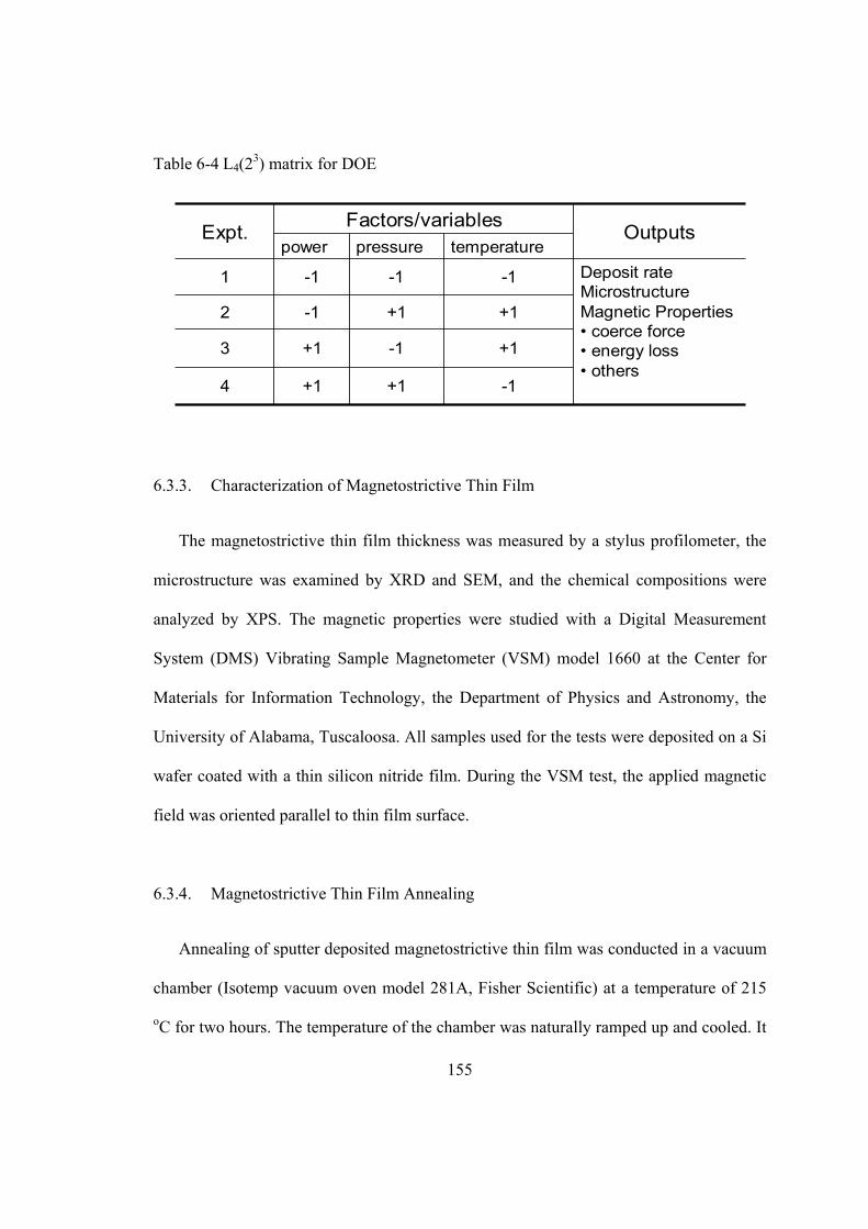
155
Table 6-4 L4(23) matrix for DOE
-1+1+14
+1-1+13
+1+1-12
Deposit rateMicrostructureMagnetic Properties• coerce force• energy loss• others
-1-1-11
temperaturepressurepowerOutputsFactors/variablesExpt.
6.3.3. Characterization of Magnetostrictive Thin Film
The magnetostrictive thin film thickness was measured by a stylus profilometer, the
microstructure was examined by XRD and SEM, and the chemical compositions were
analyzed by XPS. The magnetic properties were studied with a Digital Measurement
System (DMS) Vibrating Sample Magnetometer (VSM) model 1660 at the Center for
Materials for Information Technology, the Department of Physics and Astronomy, the
University of Alabama, Tuscaloosa. All samples used for the tests were deposited on a Si
wafer coated with a thin silicon nitride film. During the VSM test, the applied magnetic
field was oriented parallel to thin film surface.
6.3.4. Magnetostrictive Thin Film Annealing
Annealing of sputter deposited magnetostrictive thin film was conducted in a vacuum
chamber (Isotemp vacuum oven model 281A, Fisher Scientific) at a temperature of 215
oC for two hours. The temperature of the chamber was naturally ramped up and cooled. It
156
typically takes an hour to ramp up from room temperature to 215 oC. Samples were
placed in the vacuumed chamber overnight for cooling to room temperature.
6.3.5. Microfabrication of Magnetostrictive Sensors
Three types of sensors were fabricated by bulk and surface micromachining processes
in the Alabama Microelectronics Science and Technology Center (AMSTC) in the
Electrical and Computer Engineering Department, Auburn University. Cantilever and
bridge sensors were designed in various sizes. The process for fabrication of these types
of sensor is relatively complex, and step-by-step procedures are depicted in Fig. 6-6. Note
the deposition of SiC as an encapsulating layer to block the Au surfaces where it is not an
actively required.
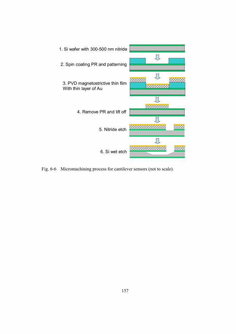
157
1. Si wafer with 300-500 nm nitride
3. PVD magnetostrictive thin filmWith thin layer of Au
2. Spin coating PR and patterning
4. Remove PR and lift off
5. Nitride etch
6. Si wet etch
Fig. 6-6 Micromachining process for cantilever sensors (not to scale).
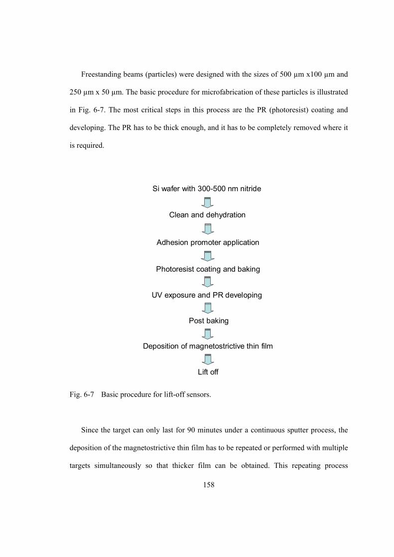
158
Freestanding beams (particles) were designed with the sizes of 500 µm x100 µm and
250 µm x 50 µm. The basic procedure for microfabrication of these particles is illustrated
in Fig. 6-7. The most critical steps in this process are the PR (photoresist) coating and
developing. The PR has to be thick enough, and it has to be completely removed where it
is required.
Si wafer with 300-500 nm nitride
Clean and dehydration
Adhesion promoter application
Photoresist coating and baking
UV exposure and PR developing
Post baking
Deposition of magnetostrictive thin film
Lift off
Fig. 6-7 Basic procedure for lift-off sensors.
Since the target can only last for 90 minutes under a continuous sputter process, the
deposition of the magnetostrictive thin film has to be repeated or performed with multiple
targets simultaneously so that thicker film can be obtained. This repeating process
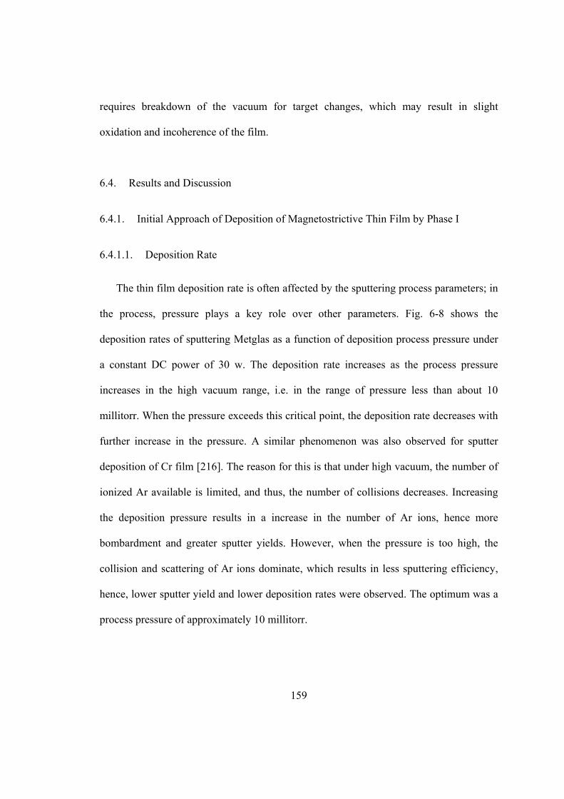
159
requires breakdown of the vacuum for target changes, which may result in slight
oxidation and incoherence of the film.
6.4. Results and Discussion
6.4.1. Initial Approach of Deposition of Magnetostrictive Thin Film by Phase I
6.4.1.1. Deposition Rate
The thin film deposition rate is often affected by the sputtering process parameters; in
the process, pressure plays a key role over other parameters. Fig. 6-8 shows the
deposition rates of sputtering Metglas as a function of deposition process pressure under
a constant DC power of 30 w. The deposition rate increases as the process pressure
increases in the high vacuum range, i.e. in the range of pressure less than about 10
millitorr. When the pressure exceeds this critical point, the deposition rate decreases with
further increase in the pressure. A similar phenomenon was also observed for sputter
deposition of Cr film [216]. The reason for this is that under high vacuum, the number of
ionized Ar available is limited, and thus, the number of collisions decreases. Increasing
the deposition pressure results in a increase in the number of Ar ions, hence more
bombardment and greater sputter yields. However, when the pressure is too high, the
collision and scattering of Ar ions dominate, which results in less sputtering efficiency,
hence, lower sputter yield and lower deposition rates were observed. The optimum was a
process pressure of approximately 10 millitorr.
160
0.40
0.50
0.60
0.70
0.80
0.90
1.00
0 3 6 9 12 15 18 21
Deposition process pressure (mT)
Nor
mal
ized
dep
ositi
on ra
te
Fig. 6-8 Deposition rate as a function of process pressure change.
6.4.1.2. Surface Morphology and Crystal Structure of Deposited Magnetostrictive Thin
Films
Three samples deposited under 5 mT, 10 mT and 20 mT at a constant power of 30
watts were characterized using SEM, XRD and VSM. The surface images of those three
samples are shown in Fig. 6-9, note the different magnifications employed in the imaging.
It was evident that the surface roughness increases as the process pressure increases. Very
fine particles are observed at the pressure of 5 mT. This result may be attributed to the
collision and scatter effect. Sputtered atoms have higher energy under lower pressure;
consequently, the film exhibits fine and dense particles. Additionally, in a higher vacuum,
the higher kinetic energy of sputtered atoms may have
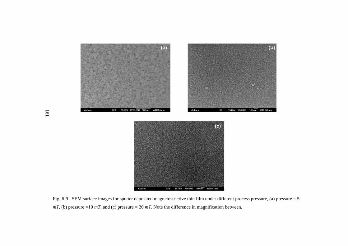
161
Fig. 6-9 SEM surface images for sputter deposited magnetostrictive thin film under different process pressure, (a) pressure = 5
mT, (b) pressure =10 mT, and (c) pressure = 20 mT. Note the difference in magnification between.
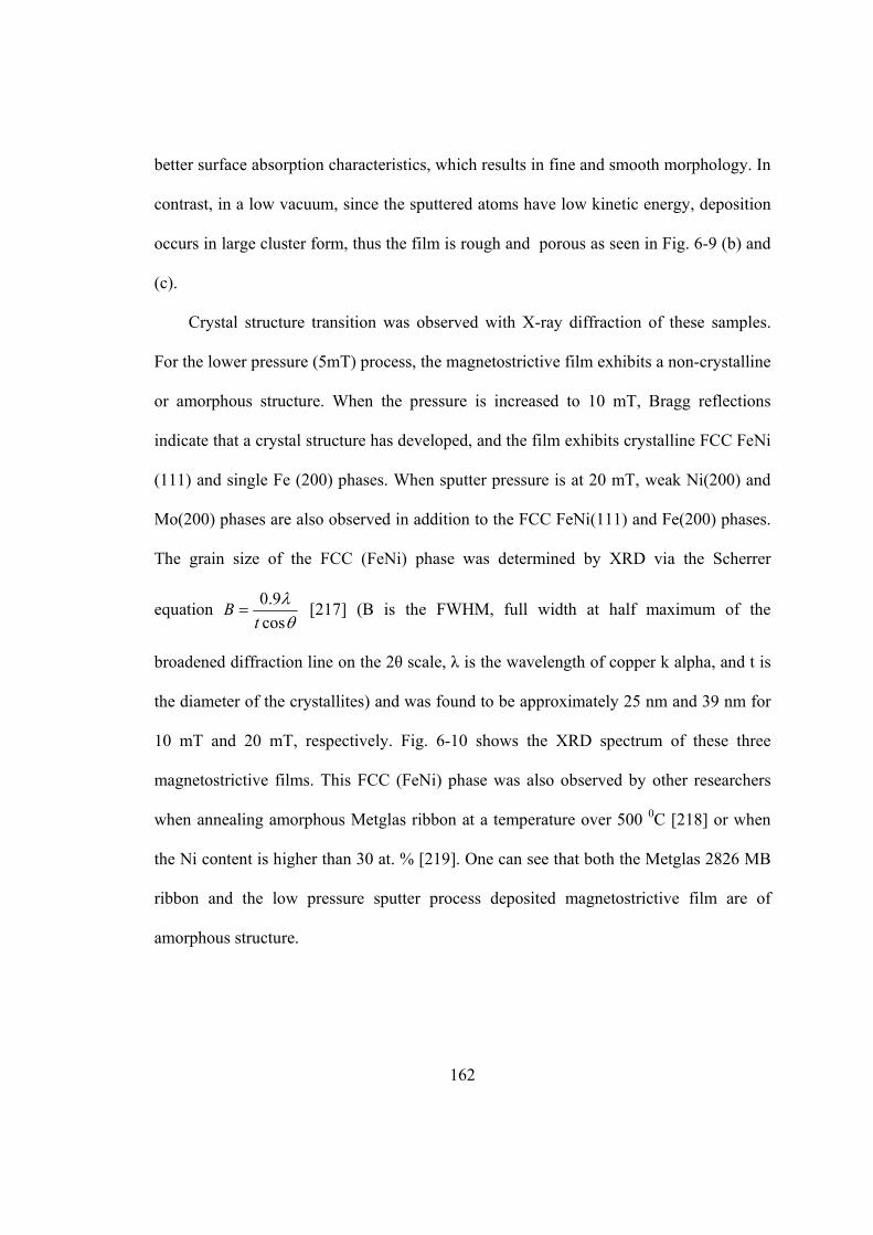
162
better surface absorption characteristics, which results in fine and smooth morphology. In
contrast, in a low vacuum, since the sputtered atoms have low kinetic energy, deposition
occurs in large cluster form, thus the film is rough and porous as seen in Fig. 6-9 (b) and
(c).
Crystal structure transition was observed with X-ray diffraction of these samples.
For the lower pressure (5mT) process, the magnetostrictive film exhibits a non-crystalline
or amorphous structure. When the pressure is increased to 10 mT, Bragg reflections
indicate that a crystal structure has developed, and the film exhibits crystalline FCC FeNi
(111) and single Fe (200) phases. When sputter pressure is at 20 mT, weak Ni(200) and
Mo(200) phases are also observed in addition to the FCC FeNi(111) and Fe(200) phases.
The grain size of the FCC (FeNi) phase was determined by XRD via the Scherrer
equation θλ
cos9.0
tB = [217] (B is the FWHM, full width at half maximum of the
broadened diffraction line on the 2θ scale, λ is the wavelength of copper k alpha, and t is
the diameter of the crystallites) and was found to be approximately 25 nm and 39 nm for
10 mT and 20 mT, respectively. Fig. 6-10 shows the XRD spectrum of these three
magnetostrictive films. This FCC (FeNi) phase was also observed by other researchers
when annealing amorphous Metglas ribbon at a temperature over 500 0C [218] or when
the Ni content is higher than 30 at. % [219]. One can see that both the Metglas 2826 MB
ribbon and the low pressure sputter process deposited magnetostrictive film are of
amorphous structure.
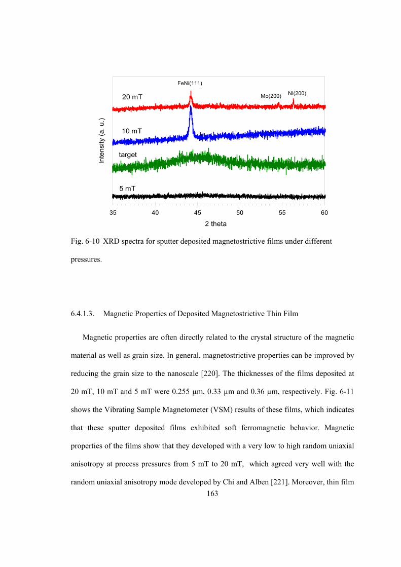
163
35 40 45 50 55 60
2 theta
Inte
nsity
(a. u
.)
FeNi(111)
Mo(200) Ni(200)
5 mT
target
10 mT
20 mT
Fig. 6-10 XRD spectra for sputter deposited magnetostrictive films under different
pressures.
6.4.1.3. Magnetic Properties of Deposited Magnetostrictive Thin Film
Magnetic properties are often directly related to the crystal structure of the magnetic
material as well as grain size. In general, magnetostrictive properties can be improved by
reducing the grain size to the nanoscale [220]. The thicknesses of the films deposited at
20 mT, 10 mT and 5 mT were 0.255 µm, 0.33 µm and 0.36 µm, respectively. Fig. 6-11
shows the Vibrating Sample Magnetometer (VSM) results of these films, which indicates
that these sputter deposited films exhibited soft ferromagnetic behavior. Magnetic
properties of the films show that they developed with a very low to high random uniaxial
anisotropy at process pressures from 5 mT to 20 mT, which agreed very well with the
random uniaxial anisotropy mode developed by Chi and Alben [221]. Moreover, thin film
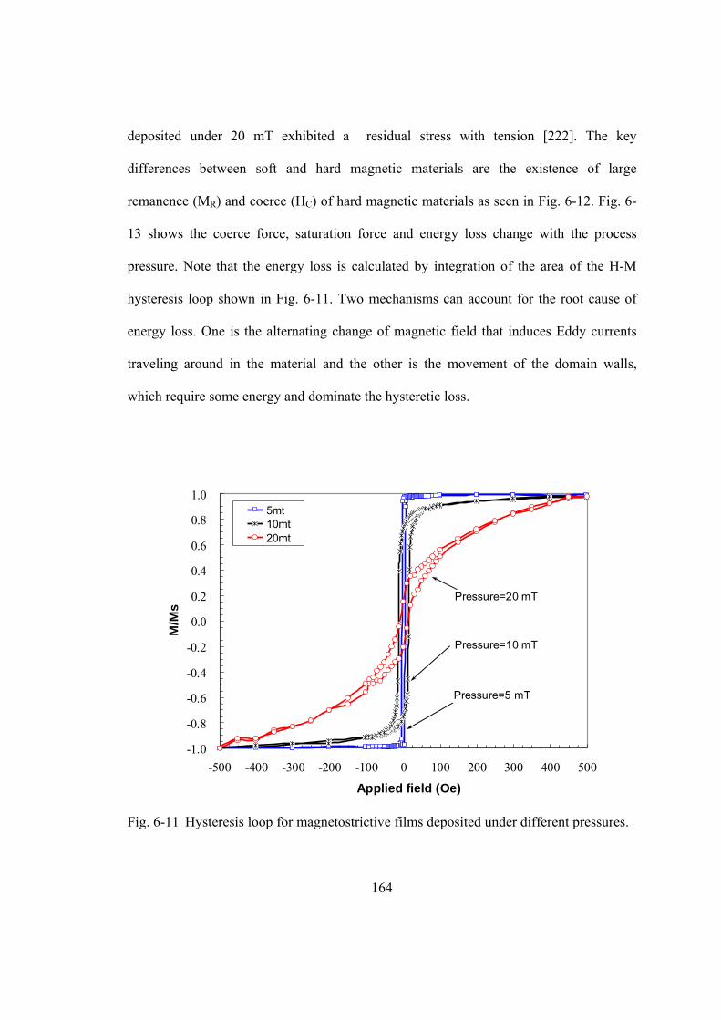
164
deposited under 20 mT exhibited a residual stress with tension [222]. The key
differences between soft and hard magnetic materials are the existence of large
remanence (MR) and coerce (HC) of hard magnetic materials as seen in Fig. 6-12. Fig. 6-
13 shows the coerce force, saturation force and energy loss change with the process
pressure. Note that the energy loss is calculated by integration of the area of the H-M
hysteresis loop shown in Fig. 6-11. Two mechanisms can account for the root cause of
energy loss. One is the alternating change of magnetic field that induces Eddy currents
traveling around in the material and the other is the movement of the domain walls,
which require some energy and dominate the hysteretic loss.
-1.0
-0.8
-0.6
-0.4
-0.2
0.0
0.2
0.4
0.6
0.8
1.0
-500 -400 -300 -200 -100 0 100 200 300 400 500
Applied field (Oe)
M/M
s
5mt10mt20mt
Pressure=5 mT
Pressure=10 mT
Pressure=20 mT
Fig. 6-11 Hysteresis loop for magnetostrictive films deposited under different pressures.
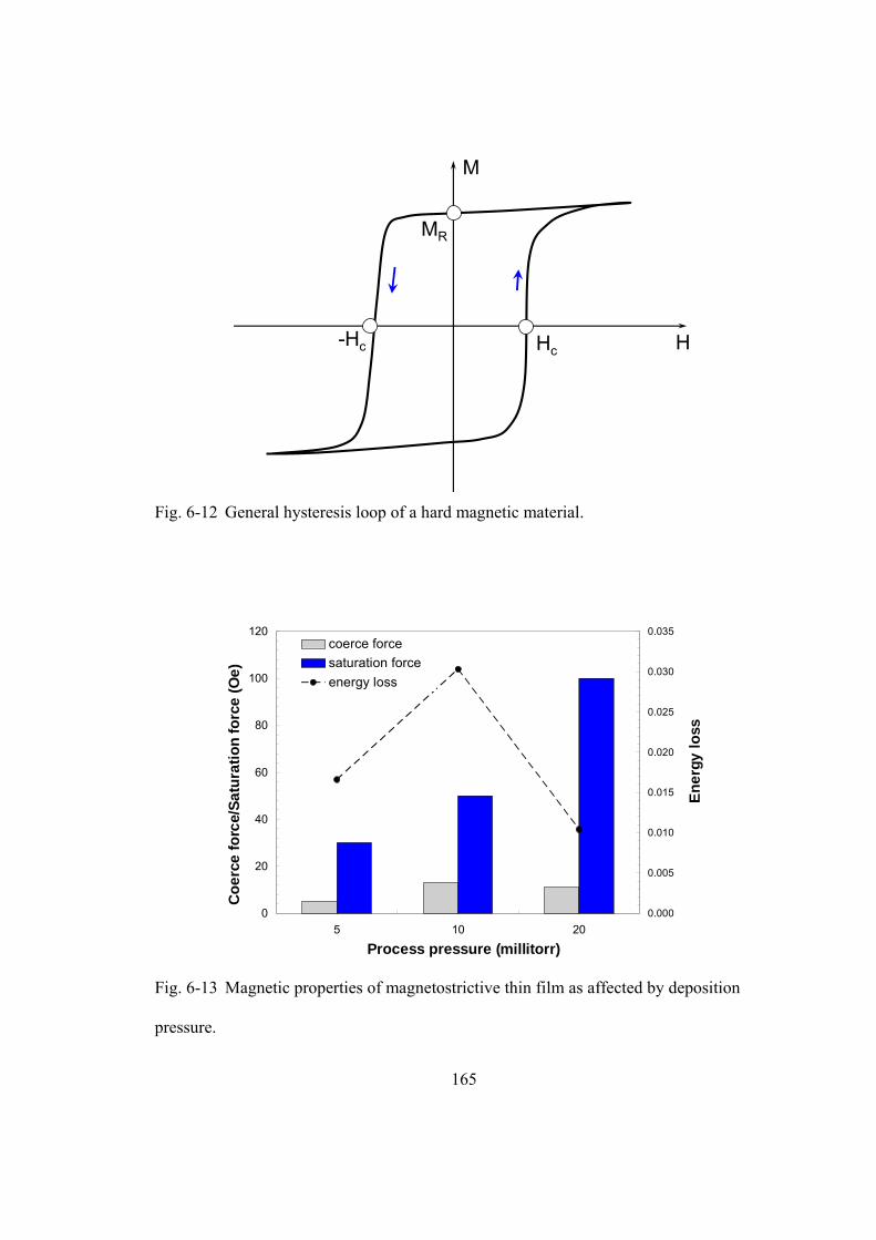
165
HHc-Hc
MR
M
Fig. 6-12 General hysteresis loop of a hard magnetic material.
0
20
40
60
80
100
120
5 10 20
Process pressure (mT)
Coe
rce
forc
e/sa
tura
tion
forc
e (O
e)
0.000
0.005
0.010
0.015
0.020
0.025
0.030
0.035
Ener
gy lo
ss
coerce forcesaturation forceenergy loss
Process pressure (millitorr)
Coe
rce
forc
e/Sa
tura
tion
forc
e (O
e)
Ener
gy lo
ss
Fig. 6-13 Magnetic properties of magnetostrictive thin film as affected by deposition
pressure.
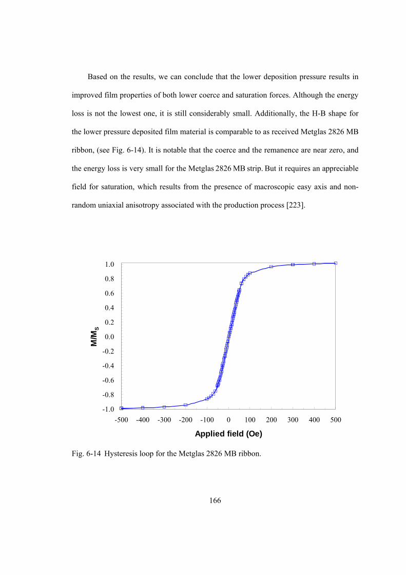
166
Based on the results, we can conclude that the lower deposition pressure results in
improved film properties of both lower coerce and saturation forces. Although the energy
loss is not the lowest one, it is still considerably small. Additionally, the H-B shape for
the lower pressure deposited film material is comparable to as received Metglas 2826 MB
ribbon, (see Fig. 6-14). It is notable that the coerce and the remanence are near zero, and
the energy loss is very small for the Metglas 2826 MB strip. But it requires an appreciable
field for saturation, which results from the presence of macroscopic easy axis and non-
random uniaxial anisotropy associated with the production process [223].
-1.0
-0.8
-0.6
-0.4
-0.2
0.0
0.2
0.4
0.6
0.8
1.0
-500 -400 -300 -200 -100 0 100 200 300 400 500
Applied field (Oe)
M/M
s
Applied field (Oe)
M/M
S
Fig. 6-14 Hysteresis loop for the Metglas 2826 MB ribbon.
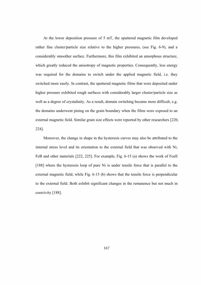
167
At the lower deposition pressure of 5 mT, the sputtered magnetic film developed
rather fine cluster/particle size relative to the higher pressures, (see Fig. 6-9), and a
considerably smoother surface. Furthermore, this film exhibited an amorphous structure,
which greatly reduced the anisotropy of magnetic properties. Consequently, less energy
was required for the domains to switch under the applied magnetic field, i.e. they
switched more easily. In contrast, the sputtered magnetic films that were deposited under
higher pressure exhibited rough surfaces with considerably larger cluster/particle size as
well as a degree of crystalinity. As a result, domain switching became more difficult, e.g.
the domains underwent pining on the grain boundary when the films were exposed to an
external magnetic field. Similar grain size effects were reported by other researchers [220,
224].
Moreover, the change in shape in the hysteresis curves may also be attributed to the
internal stress level and its orientation to the external field that was observed with Ni,
FeB and other materials [222, 225]. For example, Fig. 6-15 (a) shows the work of Foell
[188] where the hysteresis loop of pure Ni is under tensile force that is parallel to the
external magnetic field, while Fig. 6-15 (b) shows that the tensile force is perpendicular
to the external field. Both exhibit significant changes in the remanence but not much in
coercivity [188].
168
Fig. 6-15 B-H curves of pure Ni under different stress orientation to the external
magnetic field, (a) tensile stress parallel to the applied field and (b) tensile stress
perpendicular to the applied field [188].
6.4.1.4. Thin Film Composition Analysis
The compositions of the magnetostrictive thin films deposited at 5 mT, 10 mT and 20
mT were analyzed by XPS (X-ray photoelectron spectroscopy). The analysis was
conducted after sputter-etching of the specimen’s surface for 10 minutes to sample the
interior of the film. Table 6-5 summaries the XPS analysis results for the thin film and
the target material as well. There is some difference in composition between the analyzed
and supplier’s specific data on the as received Metglas 2826 MB ribbon. The atomic
composition of Fe, Ni, Mo, and B for the standard Metglas 2826 MB is 40, 38, 4 and 18,
respectively. These differences between analyzed data and supplier’s claimed data may
be a result of experimental error. A variety of compositions of sputter deposited film
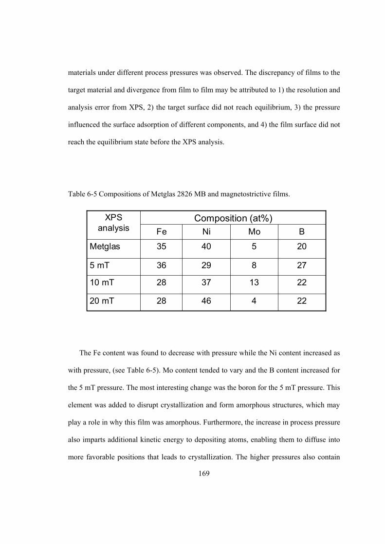
169
materials under different process pressures was observed. The discrepancy of films to the
target material and divergence from film to film may be attributed to 1) the resolution and
analysis error from XPS, 2) the target surface did not reach equilibrium, 3) the pressure
influenced the surface adsorption of different components, and 4) the film surface did not
reach the equilibrium state before the XPS analysis.
Table 6-5 Compositions of Metglas 2826 MB and magnetostrictive films.
BMoNiFe
224462820 mT
2213372810 mT
27829365 mT
2054035Metglas
Composition (at%)XPS analysis
The Fe content was found to decrease with pressure while the Ni content increased as
with pressure, (see Table 6-5). Mo content tended to vary and the B content increased for
the 5 mT pressure. The most interesting change was the boron for the 5 mT pressure. This
element was added to disrupt crystallization and form amorphous structures, which may
play a role in why this film was amorphous. Furthermore, the increase in process pressure
also imparts additional kinetic energy to depositing atoms, enabling them to diffuse into
more favorable positions that leads to crystallization. The higher pressures also contain
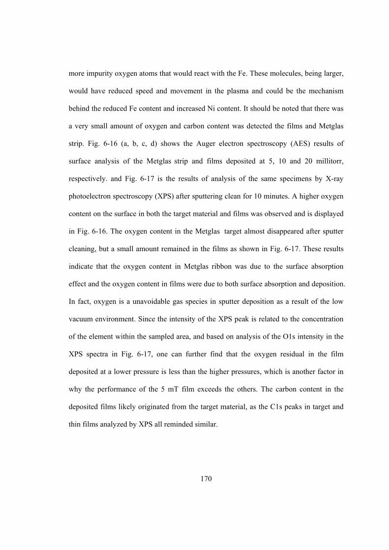
170
more impurity oxygen atoms that would react with the Fe. These molecules, being larger,
would have reduced speed and movement in the plasma and could be the mechanism
behind the reduced Fe content and increased Ni content. It should be noted that there was
a very small amount of oxygen and carbon content was detected the films and Metglas
strip. Fig. 6-16 (a, b, c, d) shows the Auger electron spectroscopy (AES) results of
surface analysis of the Metglas strip and films deposited at 5, 10 and 20 millitorr,
respectively. and Fig. 6-17 is the results of analysis of the same specimens by X-ray
photoelectron spectroscopy (XPS) after sputtering clean for 10 minutes. A higher oxygen
content on the surface in both the target material and films was observed and is displayed
in Fig. 6-16. The oxygen content in the Metglas target almost disappeared after sputter
cleaning, but a small amount remained in the films as shown in Fig. 6-17. These results
indicate that the oxygen content in Metglas ribbon was due to the surface absorption
effect and the oxygen content in films were due to both surface absorption and deposition.
In fact, oxygen is a unavoidable gas species in sputter deposition as a result of the low
vacuum environment. Since the intensity of the XPS peak is related to the concentration
of the element within the sampled area, and based on analysis of the O1s intensity in the
XPS spectra in Fig. 6-17, one can further find that the oxygen residual in the film
deposited at a lower pressure is less than the higher pressures, which is another factor in
why the performance of the 5 mT film exceeds the others. The carbon content in the
deposited films likely originated from the target material, as the C1s peaks in target and
thin films analyzed by XPS all reminded similar.
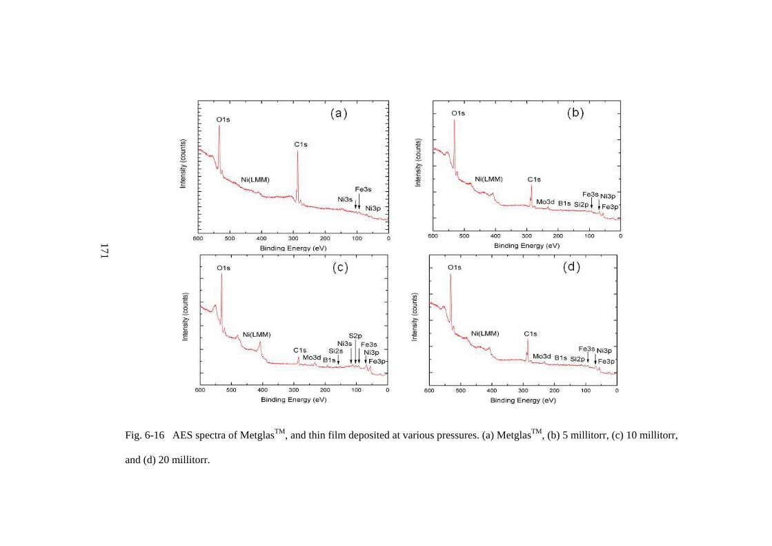
171
Fig. 6-16 AES spectra of MetglasTM, and thin film deposited at various pressures. (a) MetglasTM, (b) 5 millitorr, (c) 10 millitorr,
and (d) 20 millitorr.
172
Fig. 6-17 XPS spectra of MetglasTM, and thin film deposited at various pressures. (a) MetglasTM, (b) 5 millitorr, (c) 10 millitorr,
and (d) 20 millitorr.
173
6.4.2. DOE (Design of Experiment) Approach of Sputter Deposition by Phase II
6.4.2.1. Deposition Rate and Surface Morphology Influenced by Various Factors
Thin film deposition rate is frequently manipulated by the sputtering power and
sputtering pressure. Substrate heating temperature is another parameter that affects the
deposition rate by altering the film properties, e.g. the density, crystallinity, composition,
etc. Fig. 6-18 shows the deposition rate change with various factors. It is straight forward
to understand that the deposition rate increases with increasing the sputtering power. The
pressure effect follows the phenomenon observed and has been explained in section 6.4.1.
When the temperature increases, there is more thermal energy available, which may
promote film density. Hence, the deposition rate decreases with increasing temperature.
Fig. 6-19 shows the surface morphologies of the films examined by SEM. Note the
different magnifications employed in the imaging. Very fine particles and a smooth
surface were observed for films that were deposited under conditions of experiments (1)
and (4) in Table 6-4, while larger particle and rough surface were developed in films that
were deposited under conditions (2) and (3). It is clear that the higher temperatures of
conditions (2) and (3) resulted in coarser clusters/particles and rougher surfaces.
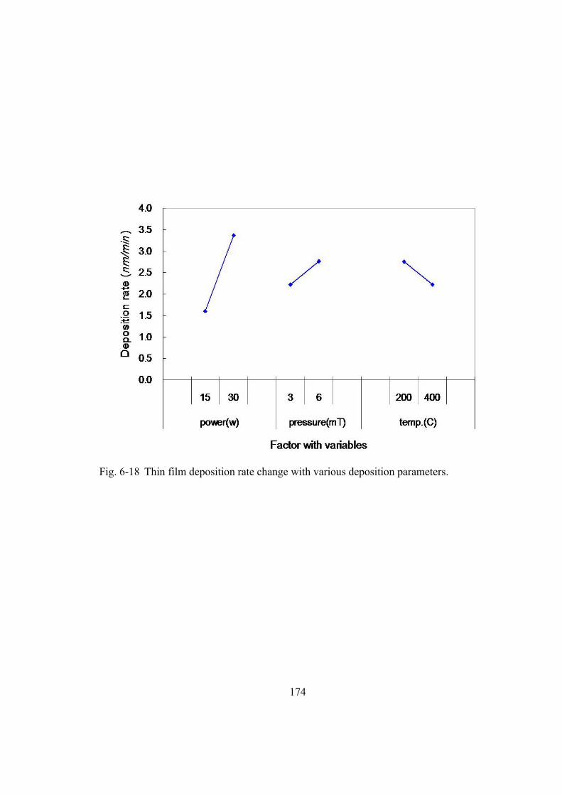
174
Fig. 6-18 Thin film deposition rate change with various deposition parameters.
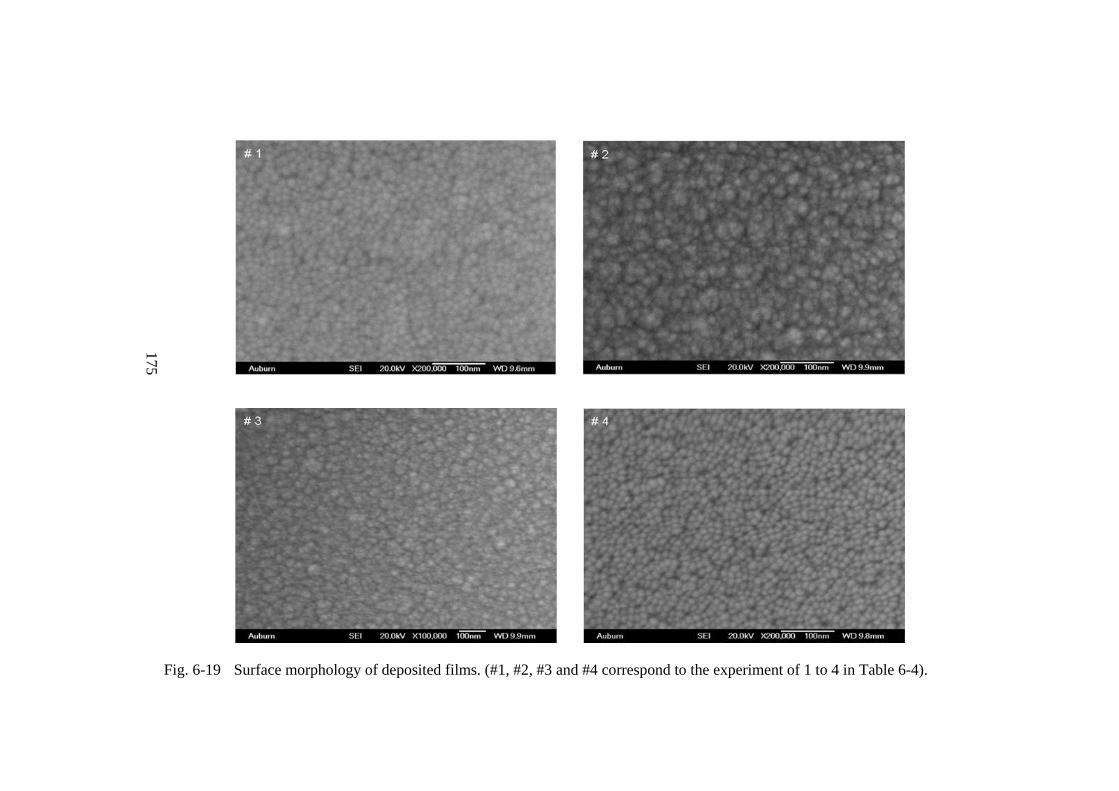
175
Fig. 6-19 Surface morphology of deposited films. (#1, #2, #3 and #4 correspond to the experiment of 1 to 4 in Table 6-4).
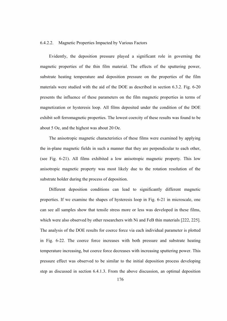
176
6.4.2.2. Magnetic Properties Impacted by Various Factors
Evidently, the deposition pressure played a significant role in governing the
magnetic properties of the thin film material. The effects of the sputtering power,
substrate heating temperature and deposition pressure on the properties of the film
materials were studied with the aid of the DOE as described in section 6.3.2. Fig. 6-20
presents the influence of these parameters on the film magnetic properties in terms of
magnetization or hysteresis loop. All films deposited under the condition of the DOE
exhibit soft ferromagnetic properties. The lowest coercity of these results was found to be
about 5 Oe, and the highest was about 20 Oe.
The anisotropic magnetic characteristics of these films were examined by applying
the in-plane magnetic fields in such a manner that they are perpendicular to each other,
(see Fig. 6-21). All films exhibited a low anisotropic magnetic property. This low
anisotropic magnetic property was most likely due to the rotation resolution of the
substrate holder during the process of deposition.
Different deposition conditions can lead to significantly different magnetic
properties. If we examine the shapes of hysteresis loop in Fig. 6-21 in microscale, one
can see all samples show that tensile stress more or less was developed in these films,
which were also observed by other researchers with Ni and FeB thin materials [222, 225].
The analysis of the DOE results for coerce force via each individual parameter is plotted
in Fig. 6-22. The coerce force increases with both pressure and substrate heating
temperature increasing, but coerce force decreases with increasing sputtering power. This
pressure effect was observed to be similar to the initial deposition process developing
step as discussed in section 6.4.1.3. From the above discussion, an optimal deposition
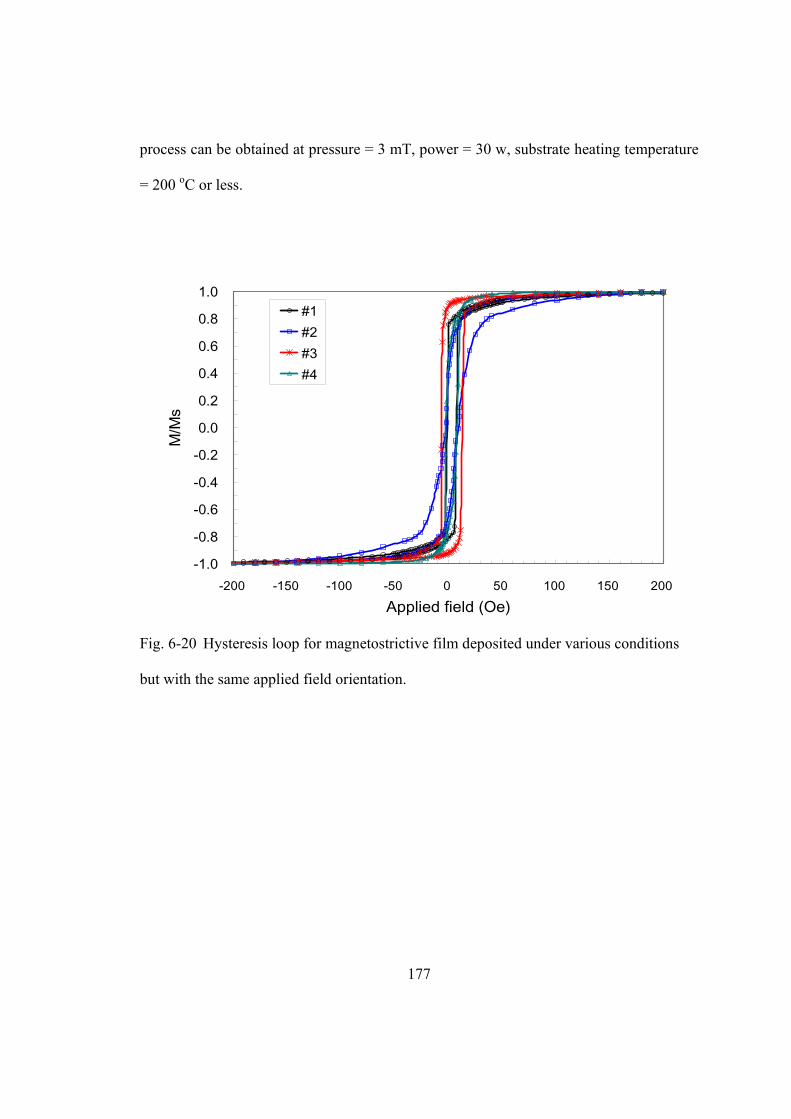
177
process can be obtained at pressure = 3 mT, power = 30 w, substrate heating temperature
= 200 oC or less.
Fig. 6-20 Hysteresis loop for magnetostrictive film deposited under various conditions
but with the same applied field orientation.
-1.0
-0.8
-0.6
-0.4
-0.2
0.0
0.2
0.4
0.6
0.8
1.0
-200 -150 -100 -50 0 50 100 150 200Applied field (Oe)
M/M
s
#1#2#3#4
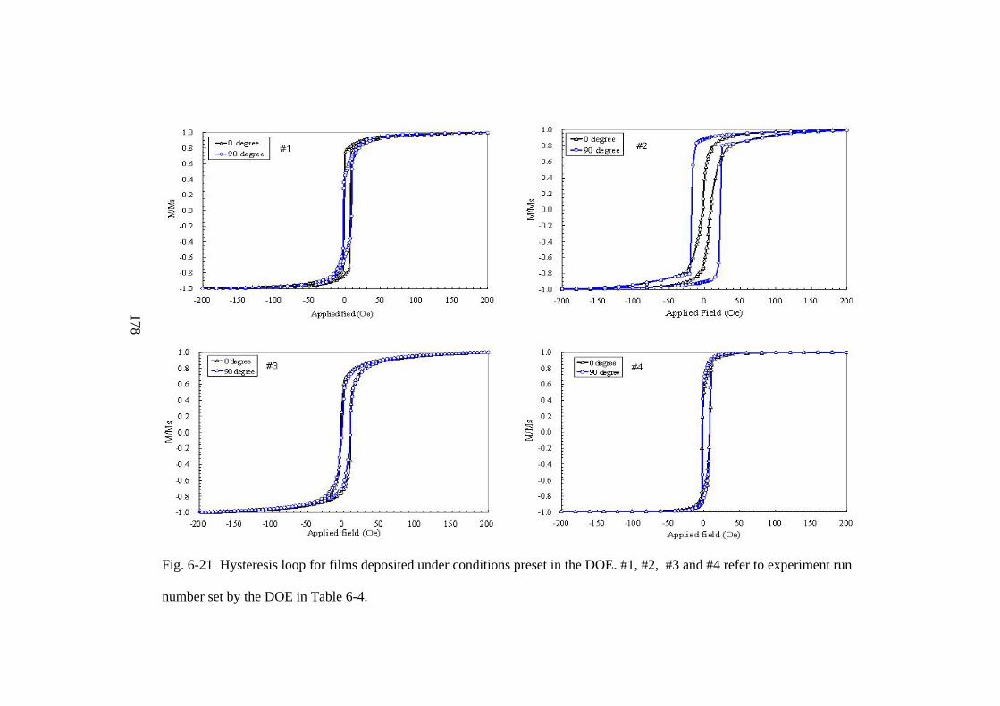
178
Fig. 6-21 Hysteresis loop for films deposited under conditions preset in the DOE. #1, #2, #3 and #4 refer to experiment run
number set by the DOE in Table 6-4.
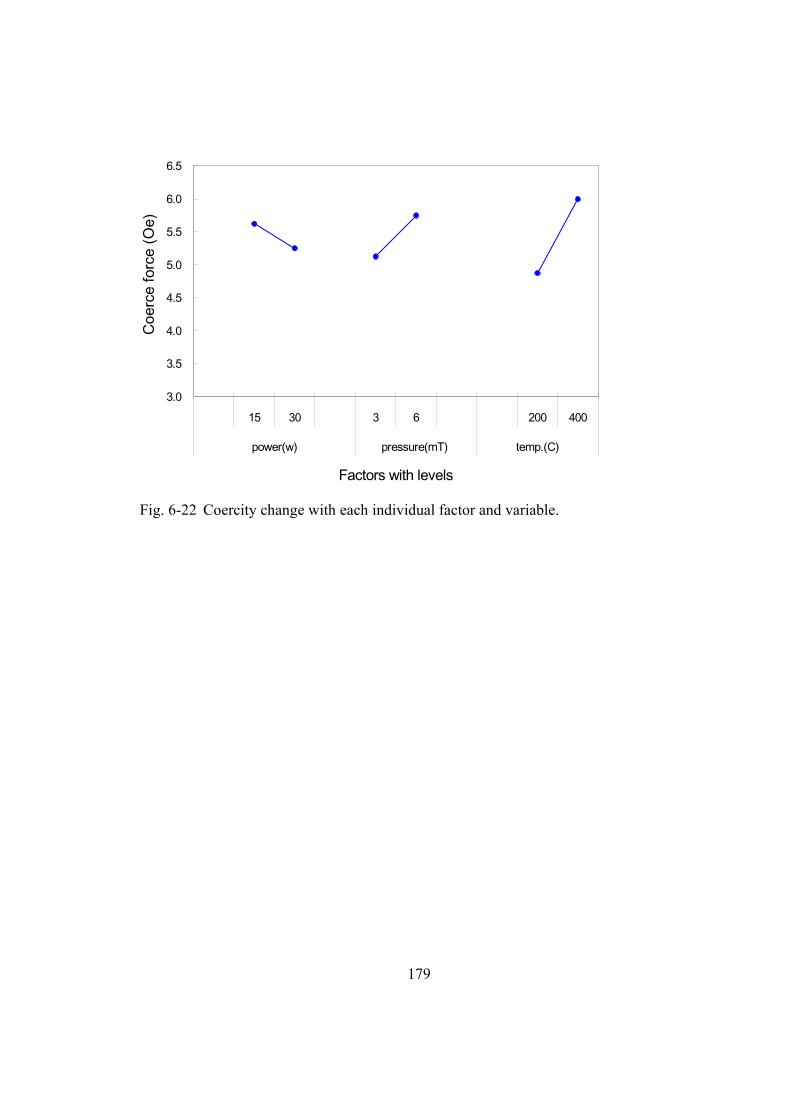
179
3.0
3.5
4.0
4.5
5.0
5.5
6.0
6.5
15 30 3 6 200 400
power(w) pressure(mT) temp.(C)
Factors with levels
Coe
rce
forc
e (O
e)
Fig. 6-22 Coercity change with each individual factor and variable.
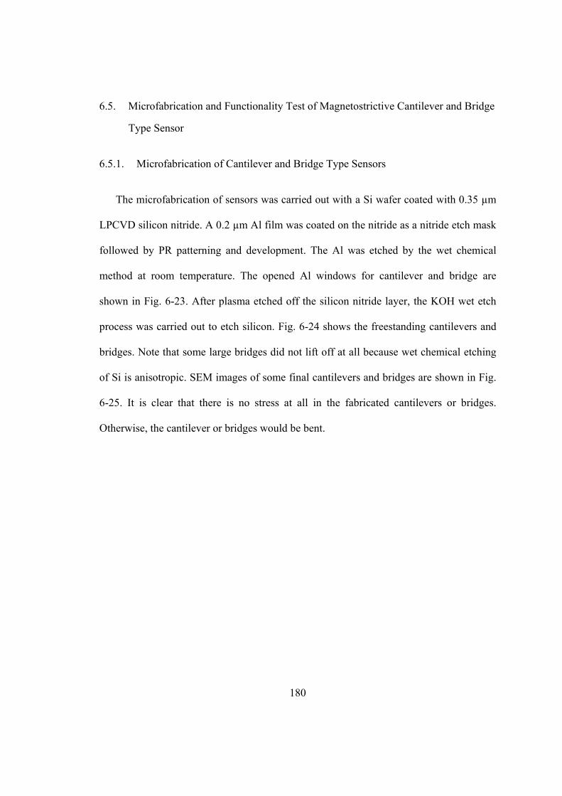
180
6.5. Microfabrication and Functionality Test of Magnetostrictive Cantilever and Bridge
Type Sensor
6.5.1. Microfabrication of Cantilever and Bridge Type Sensors
The microfabrication of sensors was carried out with a Si wafer coated with 0.35 µm
LPCVD silicon nitride. A 0.2 µm Al film was coated on the nitride as a nitride etch mask
followed by PR patterning and development. The Al was etched by the wet chemical
method at room temperature. The opened Al windows for cantilever and bridge are
shown in Fig. 6-23. After plasma etched off the silicon nitride layer, the KOH wet etch
process was carried out to etch silicon. Fig. 6-24 shows the freestanding cantilevers and
bridges. Note that some large bridges did not lift off at all because wet chemical etching
of Si is anisotropic. SEM images of some final cantilevers and bridges are shown in Fig.
6-25. It is clear that there is no stress at all in the fabricated cantilevers or bridges.
Otherwise, the cantilever or bridges would be bent.
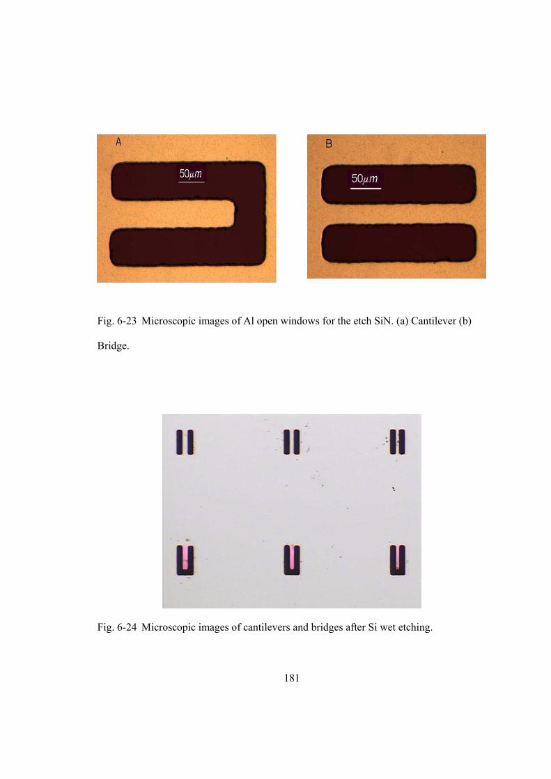
181
Fig. 6-23 Microscopic images of Al open windows for the etch SiN. (a) Cantilever (b)
Bridge.
Fig. 6-24 Microscopic images of cantilevers and bridges after Si wet etching.
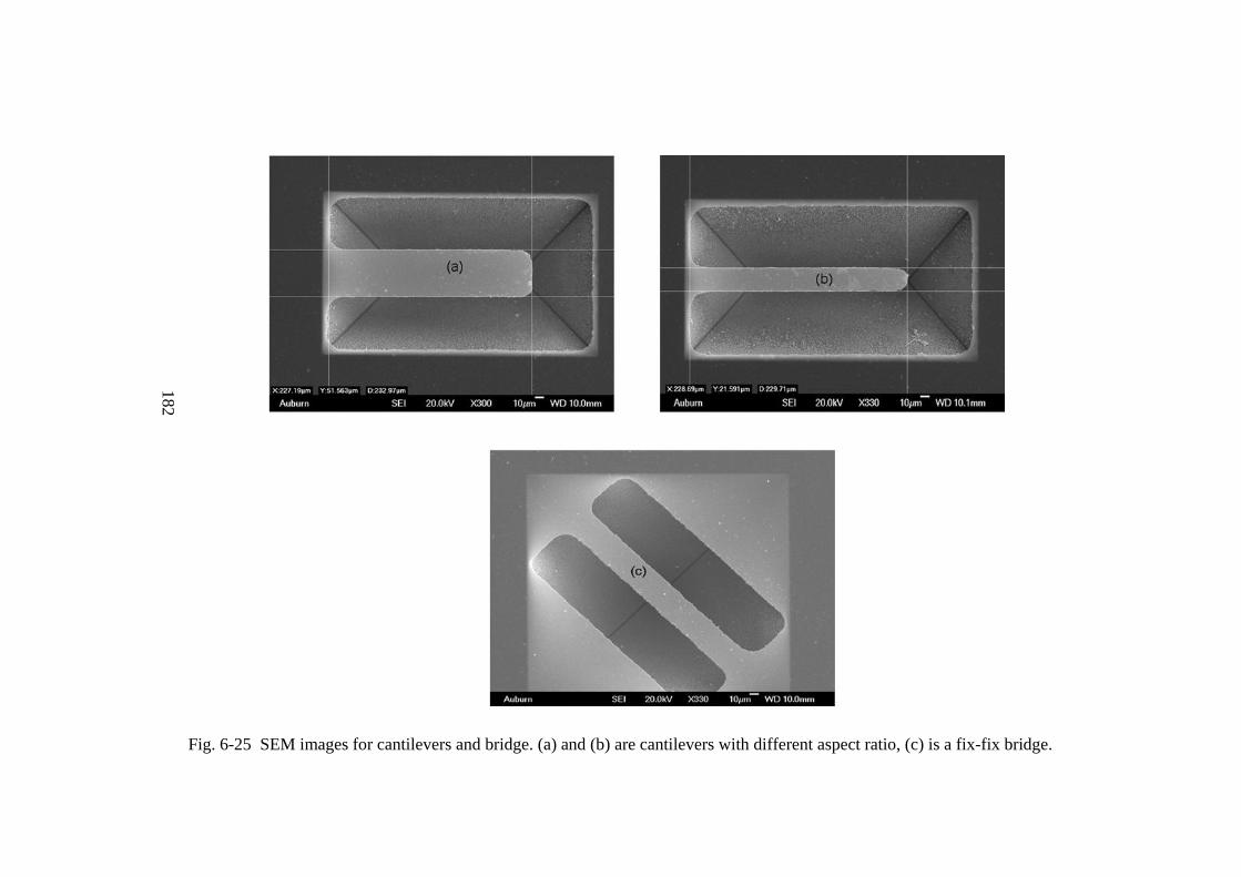
182
Fig. 6-25 SEM images for cantilevers and bridge. (a) and (b) are cantilevers with different aspect ratio, (c) is a fix-fix bridge.
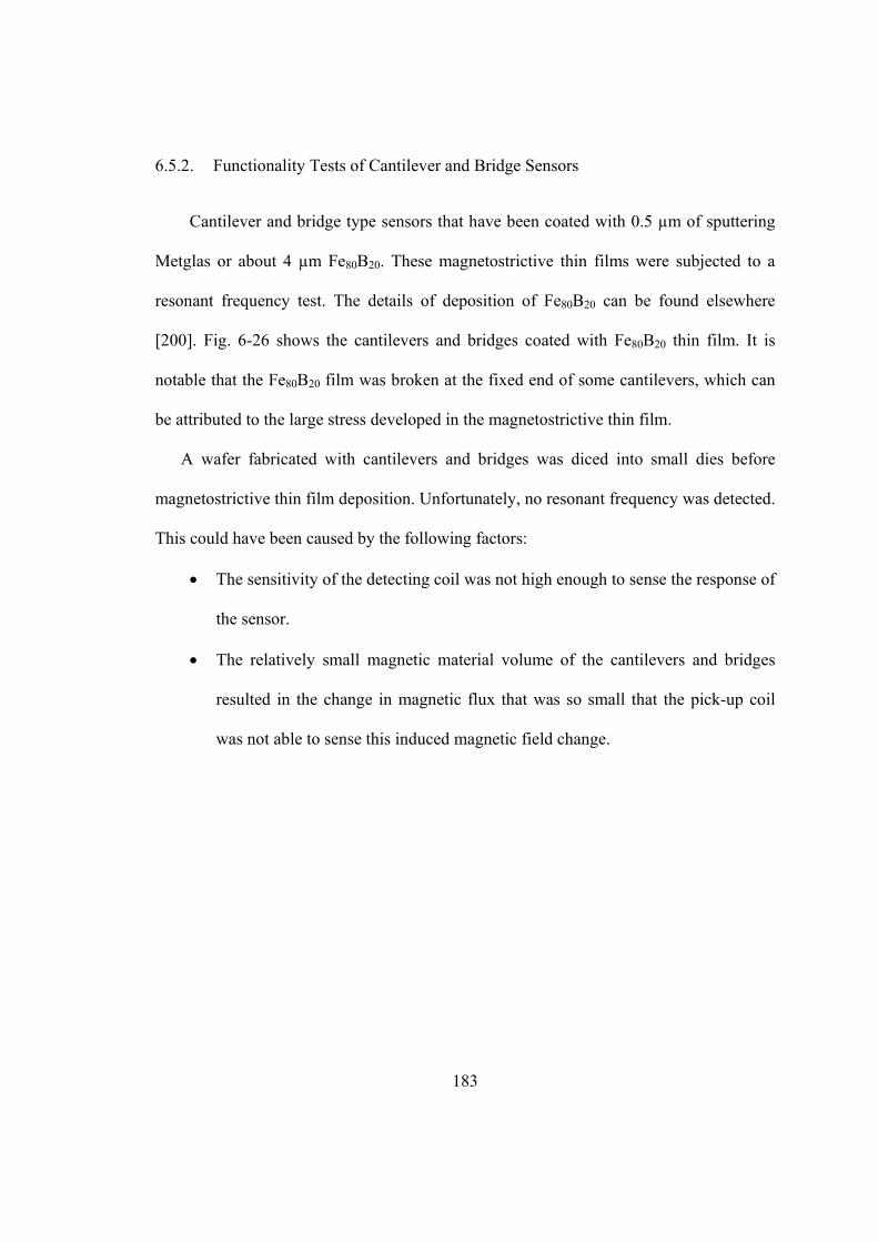
183
6.5.2. Functionality Tests of Cantilever and Bridge Sensors
Cantilever and bridge type sensors that have been coated with 0.5 µm of sputtering
Metglas or about 4 µm Fe80B20. These magnetostrictive thin films were subjected to a
resonant frequency test. The details of deposition of Fe80B20 can be found elsewhere
[200]. Fig. 6-26 shows the cantilevers and bridges coated with Fe80B20 thin film. It is
notable that the Fe80B20 film was broken at the fixed end of some cantilevers, which can
be attributed to the large stress developed in the magnetostrictive thin film.
A wafer fabricated with cantilevers and bridges was diced into small dies before
magnetostrictive thin film deposition. Unfortunately, no resonant frequency was detected.
This could have been caused by the following factors:
• The sensitivity of the detecting coil was not high enough to sense the response of
the sensor.
• The relatively small magnetic material volume of the cantilevers and bridges
resulted in the change in magnetic flux that was so small that the pick-up coil
was not able to sense this induced magnetic field change.
184
Fig. 6-26 SEM images for cantilevers and bridges coated with ~ 4 µm FeB thin films.
185
6.6. Microfabrication and Resonant Frequency Test of Magnetostrictive Freestanding
Beam (Particle)
6.6.1. Free-free ended Beam (Particle) Fabrication
The process used for the fabrication of freestanding particles was described in Fig.
6-7. The specific process is to pattern photoresist into rectangular structures possessing
the desired length and width of the freestanding beams. Fig. 6-27 illustrates these
structures on the wafer. The Metglas film is then deposited and the PR dissolved so that
the particles become freestanding and float off. In order to develop a functioning sensor,
a 100 nm thin Au film was deposited before and after the deposition of magnetostrictive
film to create a substrate for the capture film to adhere to. The process used for sputtering
the Metglas film was the optimized one as discussed in section 6.4. Multiple sputtering
processes were carried out to obtain a thicker magnetostrictive film material. The
freestanding beams or particles before lift-off are shown in Fig. 6-28. Fig. 6-29 shows the
freestanding beams before collection, from which one can see the free lift-off beams are
bent. This observation indicates that tensile stress developed in the thin film materials,
which confirms and explains the hysteresis loop shape with the measurement of magnetic
properties by VSM as shown in Figs. 6-20 and 6-21.
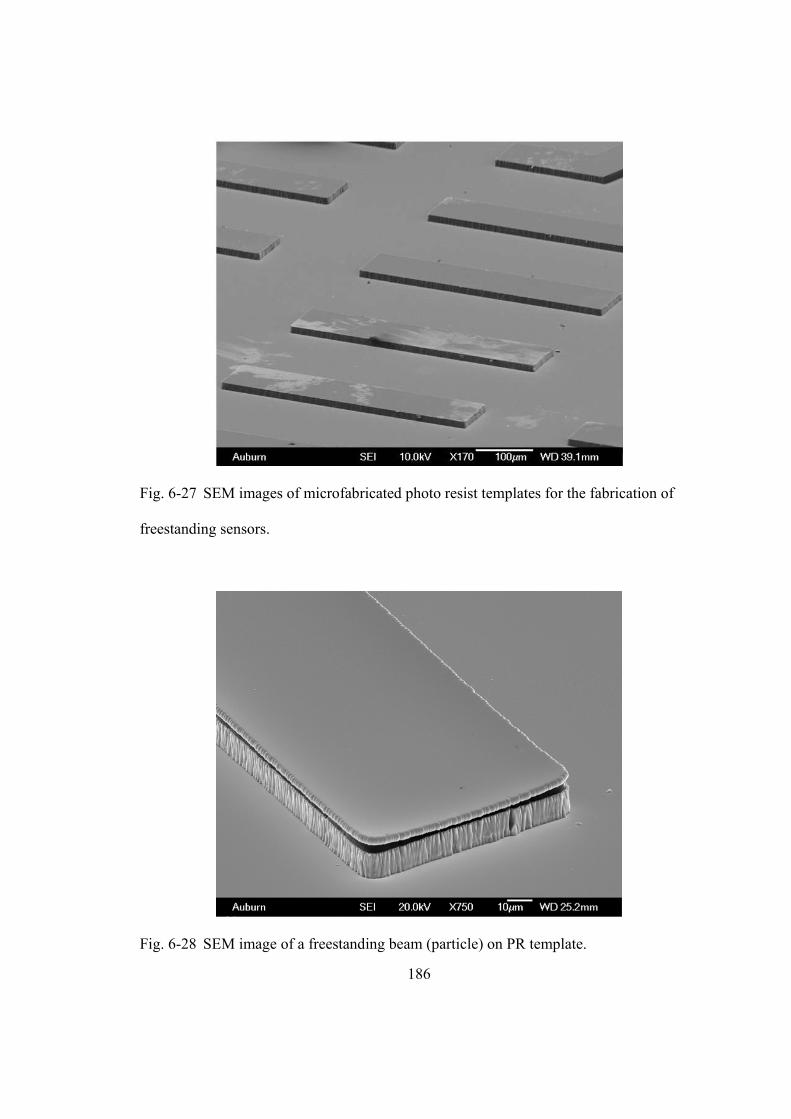
186
Fig. 6-27 SEM images of microfabricated photo resist templates for the fabrication of
freestanding sensors.
Fig. 6-28 SEM image of a freestanding beam (particle) on PR template.
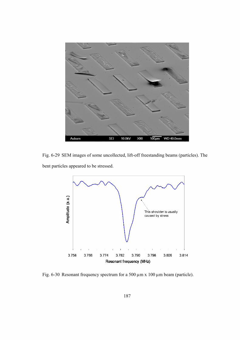
187
Fig. 6-29 SEM images of some uncollected, lift-off freestanding beams (particles). The
bent particles appeared to be stressed.
Fig. 6-30 Resonant frequency spectrum for a 500 µm x 100 µm beam (particle).
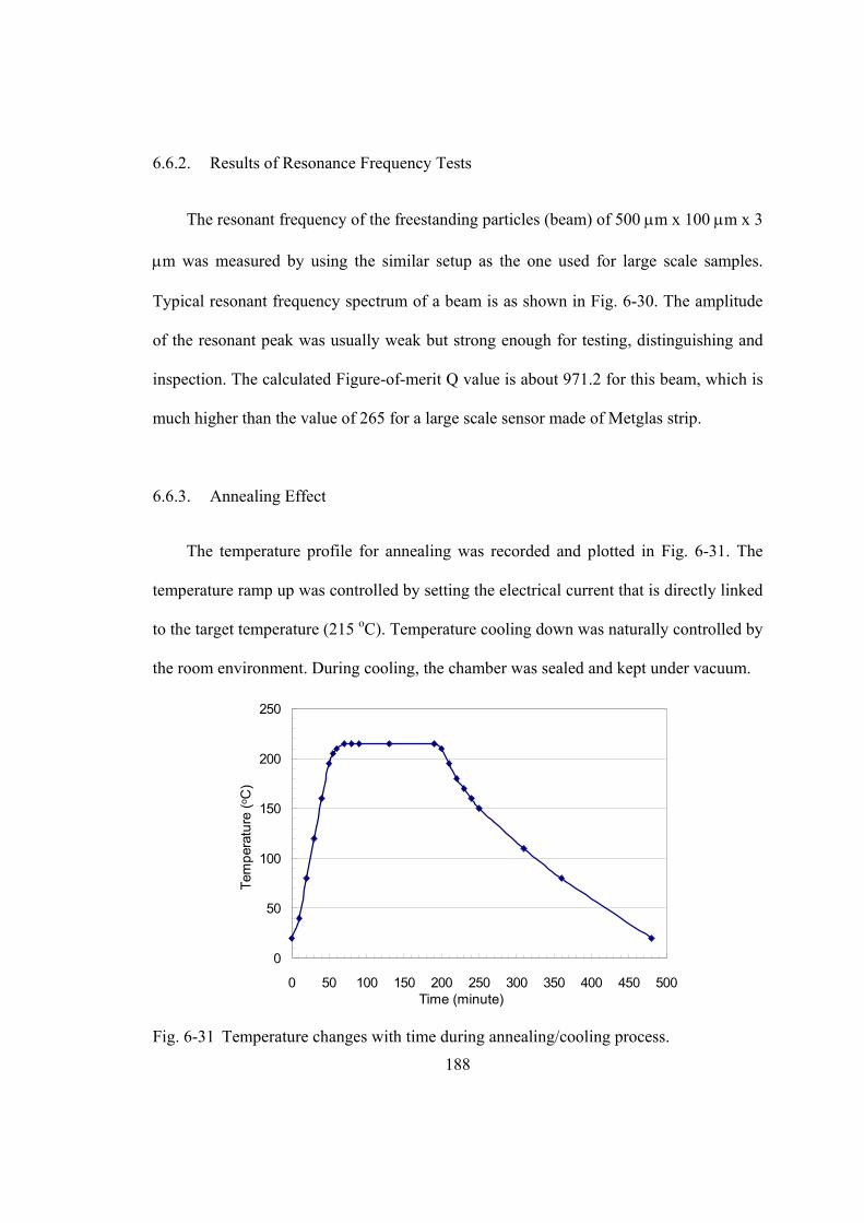
188
6.6.2. Results of Resonance Frequency Tests
The resonant frequency of the freestanding particles (beam) of 500 µm x 100 µm x 3
µm was measured by using the similar setup as the one used for large scale samples.
Typical resonant frequency spectrum of a beam is as shown in Fig. 6-30. The amplitude
of the resonant peak was usually weak but strong enough for testing, distinguishing and
inspection. The calculated Figure-of-merit Q value is about 971.2 for this beam, which is
much higher than the value of 265 for a large scale sensor made of Metglas strip.
6.6.3. Annealing Effect
The temperature profile for annealing was recorded and plotted in Fig. 6-31. The
temperature ramp up was controlled by setting the electrical current that is directly linked
to the target temperature (215 oC). Temperature cooling down was naturally controlled by
the room environment. During cooling, the chamber was sealed and kept under vacuum.
0
50
100
150
200
250
0 50 100 150 200 250 300 350 400 450 500
Tem
pera
ture
(oC
)
Time (minute)
Fig. 6-31 Temperature changes with time during annealing/cooling process.
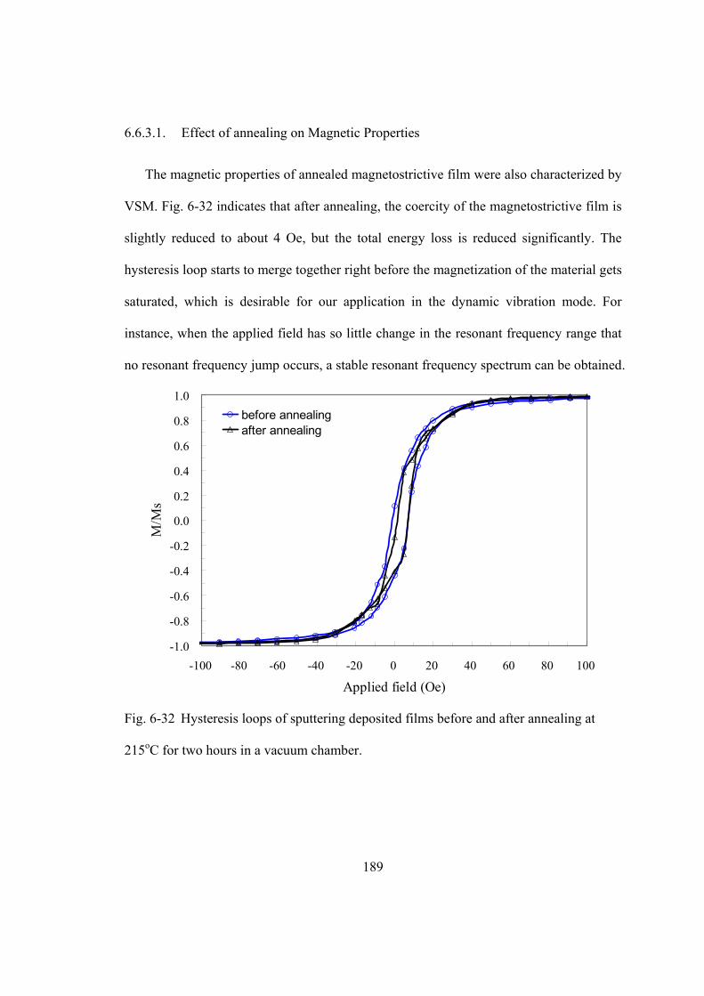
189
6.6.3.1. Effect of annealing on Magnetic Properties
The magnetic properties of annealed magnetostrictive film were also characterized by
VSM. Fig. 6-32 indicates that after annealing, the coercity of the magnetostrictive film is
slightly reduced to about 4 Oe, but the total energy loss is reduced significantly. The
hysteresis loop starts to merge together right before the magnetization of the material gets
saturated, which is desirable for our application in the dynamic vibration mode. For
instance, when the applied field has so little change in the resonant frequency range that
no resonant frequency jump occurs, a stable resonant frequency spectrum can be obtained.
-1.0
-0.8
-0.6
-0.4
-0.2
0.0
0.2
0.4
0.6
0.8
1.0
-100 -80 -60 -40 -20 0 20 40 60 80 100
Applied field (Oe)
M/M
s
before annealingafter annealing
t
Fig. 6-32 Hysteresis loops of sputtering deposited films before and after annealing at
215oC for two hours in a vacuum chamber.
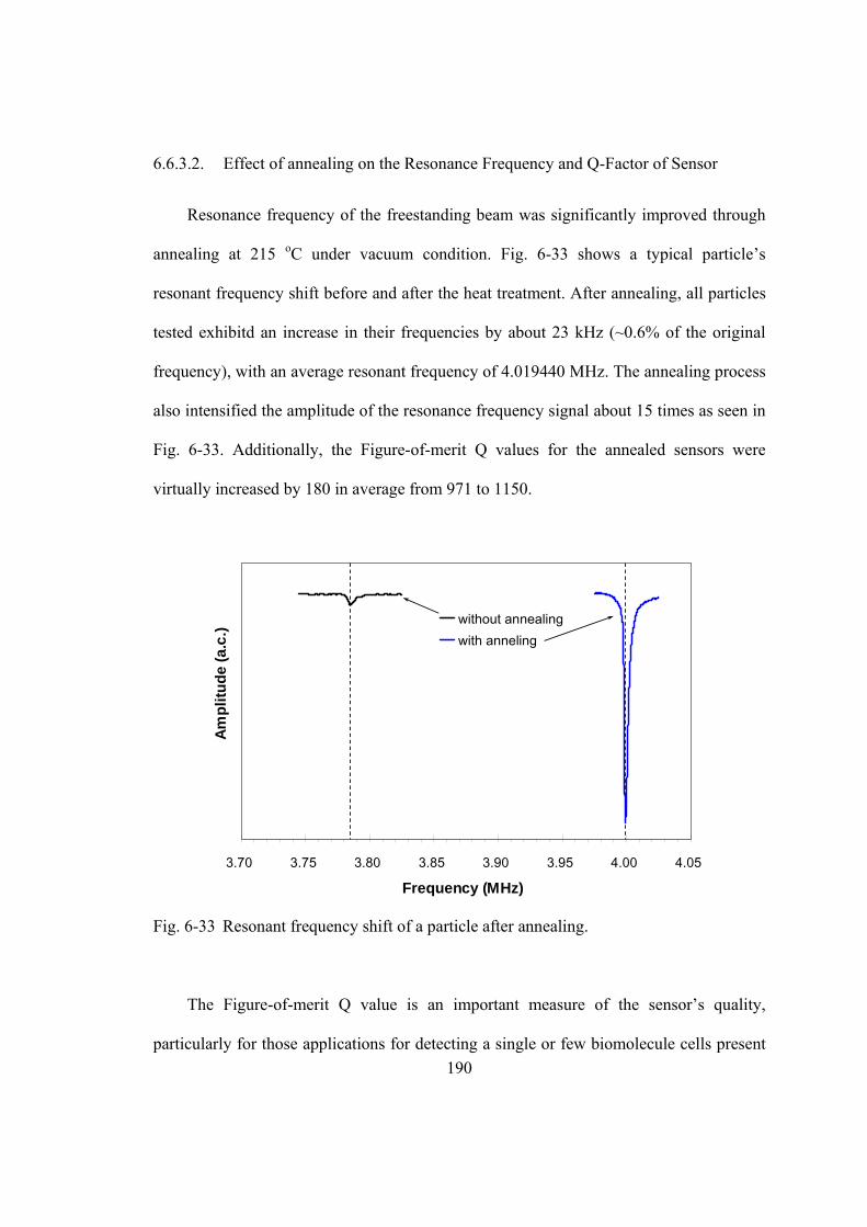
190
6.6.3.2. Effect of annealing on the Resonance Frequency and Q-Factor of Sensor
Resonance frequency of the freestanding beam was significantly improved through
annealing at 215 oC under vacuum condition. Fig. 6-33 shows a typical particle’s
resonant frequency shift before and after the heat treatment. After annealing, all particles
tested exhibitd an increase in their frequencies by about 23 kHz (~0.6% of the original
frequency), with an average resonant frequency of 4.019440 MHz. The annealing process
also intensified the amplitude of the resonance frequency signal about 15 times as seen in
Fig. 6-33. Additionally, the Figure-of-merit Q values for the annealed sensors were
virtually increased by 180 in average from 971 to 1150.
3.70 3.75 3.80 3.85 3.90 3.95 4.00 4.05
Frequency (MHz)
Ampl
itude
(a.c
.)
without annealingwith anneling
Frequency (MHz)
Ampl
itude
(a.c
.)
Fig. 6-33 Resonant frequency shift of a particle after annealing.
The Figure-of-merit Q value is an important measure of the sensor’s quality,
particularly for those applications for detecting a single or few biomolecule cells present
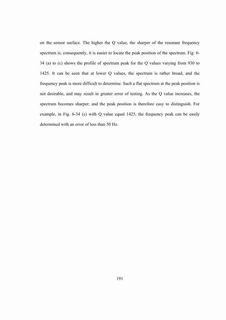
191
on the sensor surface. The higher the Q value, the sharper of the resonant frequency
spectrum is; consequently, it is easier to locate the peak position of the spectrum. Fig. 6-
34 (a) to (c) shows the profile of spectrum peak for the Q values varying from 930 to
1425. It can be seen that at lower Q values, the spectrum is rather broad, and the
frequency peak is more difficult to determine. Such a flat spectrum at the peak position is
not desirable, and may result in greater error of testing. As the Q value increases, the
spectrum becomes sharper; and the peak position is therefore easy to distinguish. For
example, in Fig. 6-34 (c) with Q value equal 1425, the frequency peak can be easily
determined with an error of less than 50 Hz.
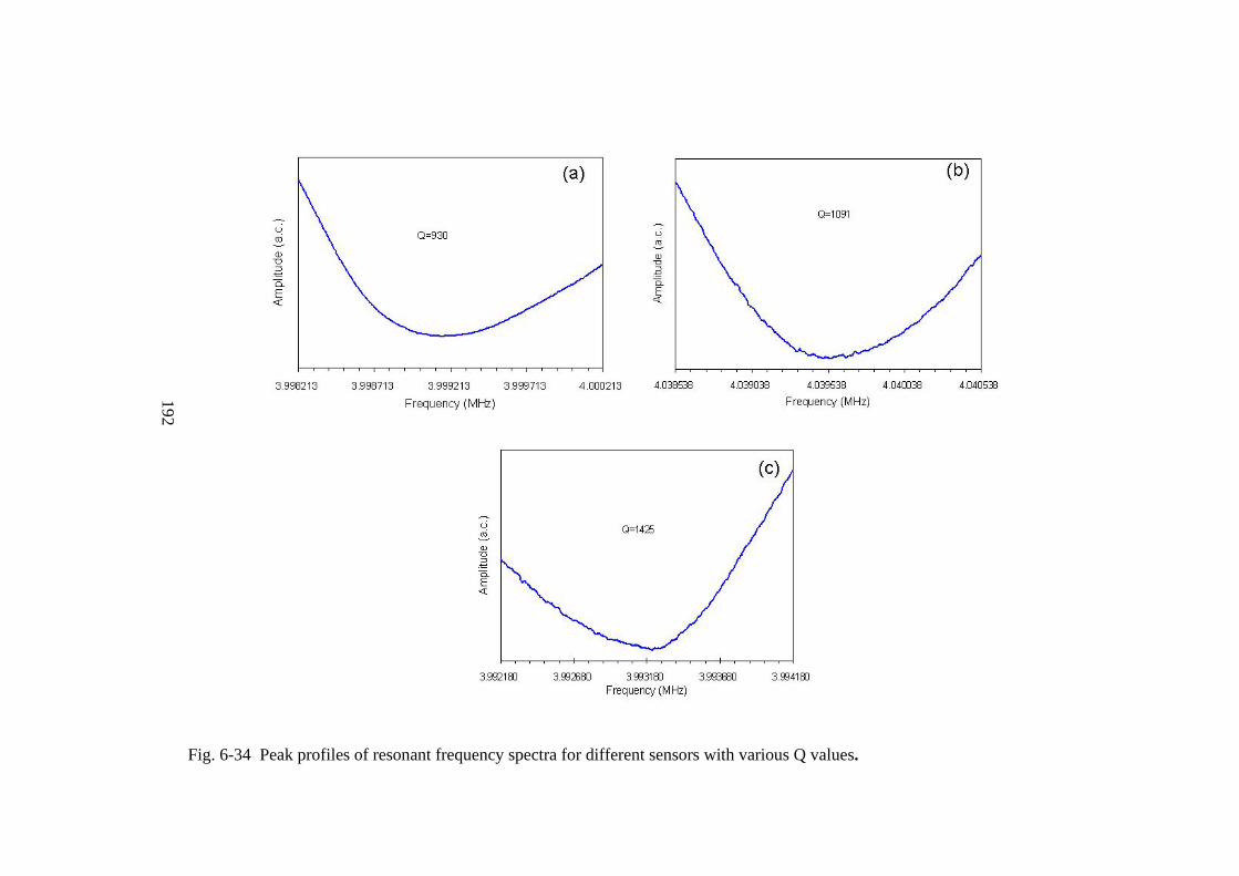
192
Fig. 6-34 Peak profiles of resonant frequency spectra for different sensors with various Q values.
193
6.6.3.3. Mechanisms on the Annealing Effects
The effect of annealing on the magnetic properties of magnetostrictive thin films and
the sensor’s performance may be attributed to an increase in the elastic modulus and a
reduction in residual stress during the annealing process. The change in the elastic
modulus of the film materials after annealing is most likely due to the defect healing.
Furthermore, the annealing treatment also released the residual stress as it can be seen
from Fig. 6-29, where the freestanding beams are bowed down due to stress developed in
the magnetostrictive film. Fig. 6-35 shows that when the stress in the longitudinal
direction of sensor is released, there is no curvature observed under SEM. However, we
do observe that the sensor still has slight curvature in the width direction upon annealing.
This effect of stress released in longitudinal direction greatly improves the sensor
performance such as amplitude of the resonance frequency peak and Q value. The
following model is suggested to elucidate the effects.
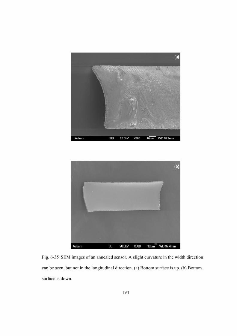
194
Fig. 6-35 SEM images of an annealed sensor. A slight curvature in the width direction
can be seen, but not in the longitudinal direction. (a) Bottom surface is up. (b) Bottom
surface is down.
a
b
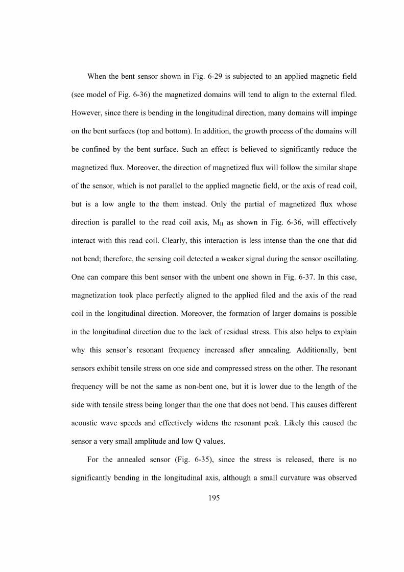
195
When the bent sensor shown in Fig. 6-29 is subjected to an applied magnetic field
(see model of Fig. 6-36) the magnetized domains will tend to align to the external filed.
However, since there is bending in the longitudinal direction, many domains will impinge
on the bent surfaces (top and bottom). In addition, the growth process of the domains will
be confined by the bent surface. Such an effect is believed to significantly reduce the
magnetized flux. Moreover, the direction of magnetized flux will follow the similar shape
of the sensor, which is not parallel to the applied magnetic field, or the axis of read coil,
but is a low angle to the them instead. Only the partial of magnetized flux whose
direction is parallel to the read coil axis, MII as shown in Fig. 6-36, will effectively
interact with this read coil. Clearly, this interaction is less intense than the one that did
not bend; therefore, the sensing coil detected a weaker signal during the sensor oscillating.
One can compare this bent sensor with the unbent one shown in Fig. 6-37. In this case,
magnetization took place perfectly aligned to the applied filed and the axis of the read
coil in the longitudinal direction. Moreover, the formation of larger domains is possible
in the longitudinal direction due to the lack of residual stress. This also helps to explain
why this sensor’s resonant frequency increased after annealing. Additionally, bent
sensors exhibit tensile stress on one side and compressed stress on the other. The resonant
frequency will be not the same as non-bent one, but it is lower due to the length of the
side with tensile stress being longer than the one that does not bend. This causes different
acoustic wave speeds and effectively widens the resonant peak. Likely this caused the
sensor a very small amplitude and low Q values.
For the annealed sensor (Fig. 6-35), since the stress is released, there is no
significantly bending in the longitudinal axis, although a small curvature was observed
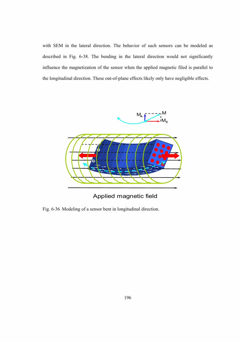
196
with SEM in the lateral direction. The behavior of such sensors can be modeled as
described in Fig. 6-38. The bending in the lateral direction would not significantly
influence the magnetization of the sensor when the applied magnetic filed is parallel to
the longitudinal direction. These out-of-plane effects likely only have negligible effects.
+
+
Applied magnetic field
MMII
MI
Fig. 6-36 Modeling of a sensor bent in longitudinal direction.
197
Applied H
Fig. 6-37 Modeling of a perfect sensor without bending.
Applied H
Fig. 6-38 Modeling of an annealed sensor that is only bent in the lateral axis, but not in
the longitudinal direction.
198
6.7. Summary
The fabrication of a Metglas sputtering target and deposition of a magnetostrictive
thin film were demonstrated in this work. The film material exhibited soft ferromagnetic
properties and low degrees of magnetic anisotropy. Deposition process studies indicated
that the magnetic properties of thin film material are very much dependent on the process
parameters, such as deposition pressure, sputtering power and substrate temperature. The
optimal deposition parameters were found to be: pressure = 3 mT, power = 30 w, and
substrate heating temperature = 200oC or room temperature.
Stress associated with the thin film during deposition was released by annealing at
215 oC for 120 minutes, which resulted in increased resonant frequency and Q factor,
aspects that are important in developing this material into a usable sensor. The resonant
frequency of microfabricated magnetostrictive sensors in both cantilevers and bridges
was not detectable by general detecting setup because the pickup coil wasnot sensitive
enough. However, a successful detection of microscale freestanding beams was
demonstrated. The sensor’s performance was significantly improved by annealing and a
model describing this effect was proposed.
199
7. CONCLUSION AND FUTURE WORK
7.1. Conclusions
This work focused on solving several issues in the development of magnetostrictive
acoustic wave sensors. Magnetostrictive material has been shown to be an excellent
material for actuation and sensing in sensors that are configured as a cantilever, bridge,
and beam. These sensors are driven by an alternating magnetic field and mass changes
are measured by monitoring changes in resonant frequency. The work addressed the
benefits of the longitudinal vibration mode, provided more precise governing equations,
and demonstrated that magnetostrictive sensors are a cheap and easy method for
measuring the thin film Young’s modulus. It also developed the optimum sputter
deposition parameters for depositing magnetostrictive films from Metglas 2826 MB
targets and illustrated how to microfabricate these structures into useful forms. Finally, it
constructed and demonstrated operation of thin film microscale resonators.
In particular, the superiority of the longitudinal mode resonance over the transverse
mode was discussed and proven. The governing equations for a thin slender beam
resonating in the longitudinal mode was modified by replacing the plane strain modulus
with the plane stress modulus for geometries associated with thin film resonators or bulk
scale resonators where thickness is significantly less than length and width. This was
accomplished through a combined experimental and numerical simulation approach
200
which not only found issues with the fundamental operation equation for the longitudinal
mode, but also clarified and confirmed that the Poisson’s ratio for commercial Metglas
2826 MB strip is 0.33. This work also aided in identifying that a cantilever sensor 250
microns in length 50 microns wide with a thickness one micron or less, should be able to
detect small amounts of mass or even a single spore or cell attached to the sensor’s
surface.
Metglas resonators were constructed and used to measure the thin film Young’s
modulus of several materials commonly used in state-of-the-art devices. The results were
confirmed using a second thin film measurement technique and demonstrated that this
technique offers a cost-effective, user-friendly and non-destructive test for thin film
properties. It also improved the methodology of determining the thin film Young’s
modulus by assuming that film density was equivalent to bulk density, which
significantly reduced the amount of error associated with the measurement.
This research also successfully developed the optimum process parameters for
magnetostrictive thin film deposition by directly sputtering a Metglas strip. The optimal
deposition parameters were found to be pressure =3 mT, power = 30 w, and a substrate
heating temperature of 200 oC or room temperature followed by annealing at 215 oC for
120 minutes. The deposited thin film material exhibited soft ferromagnetism and high
isotropic magnetic properties. Freestanding beams or particles with the size of 500 µm x
100 µm x 3 µm were fabricated by standard microfabrication process and their resonant
frequency was effectively detected. Annealing the sensors resulted in relieving residual
stress, which significantly improved performance and Q factor.
201
7.2. Future work
The successful deposition and microfabrication of thin film magnetostrictive sensors
has the potential to revolutionize the MEMS and microdevices field by enabling
remote/wireless powering and actuation of devices. Towards this goal, future work
should focus on (1) better detection of small amounts of biological agents, (2) integrating
these thin film actuators into actual devices or demonstrating their function and (3)
developing small, on-chip read coils to detect their signals.
(1) Detection of Biological Agents
• develop a sensor with both bridges and freestanding beams of varying size to
better assess attachment of biological species
• develop an algorithm that can distinguish between the number of spores or
cells attaching and their position on the platform
(2) Integration as MEMS actuators would require the following tasks
• demonstrate that magnetostrictive films are compatible with many types of
microfabrication processes
• demonstrate that magnetostrictive films retain their properties when subjected
to typical MEMS microfabrication processes
(3) Development of a small, on-chip coils would require the following tasks
• develop a 2-dimensional magnetic coil capable of applying and reading the
necessary fields
• examine employing giant magnetoresistive elements to detect fields generated
by the films
202
REFERENCES
[1] F. Qian, "Numerical Simulation and Mechanical Propeties of Free Standing Silver
Thin Film," in Materials Eng. Auburn: Auburn University, 2006, pp. 111.
[2] J. S. Bresee, V. Dietz, M. G. Patricia, L. F. Mccaig, P. S. Mead, C. Shapiro, L.
Slutsker, and R. V. Tauxe, "Food-Related Illness and Death in the United States,"
J. Environmental Health, vol. 62, 2000.
[3] P. S. Mead, L. Slutsker, V. Dietz, L. F. McCaig, J. S. Bresee, C. Shapiro, P. M.
Griffin, and R. V. Tauxe, "Food-Related Illness and Death in the United States.,"
J. Environmental Health, vol. 62, pp. 9, 2000.
[4] "Lettuce recalled over E. Coli concerns", presented at USA Today, San Francisco.
11/29/2007, [Online] available:
http://www.usatoday.com/money/industries/food/2006-10-09-lettuce_x.htm.
[5] F. Pritzker, "CDC Detailed Report on Spinach and Escherichia coli Outbreak,"
CDC, Mortality and Morbidity Weekly Report, No.55, September 27 2006.
[6] R. E. Hummel, Electronic Properties of Materials, 3rd ed. Springer, New York,
2000.
[7] Iowa State University, "Magnetostrictive Transducers, Actuators, and Sensors",
11/29/2007, [Online] available: http://www.public.iastate.edu/~terfenol/.
203
[8] Wikipedia, "Magnetostriction", 11/29/2007, [Online] available:
http://en.wikipedia.org/wiki/Magnetostriction.
[9] G. E. Fish, "Soft magnetic materials," Proc. IEEE, vol. 78, pp. 947-972, 1990.
[10] Metglas Inc., 11/29/2007, " Magnetic Alloy 2826 MB, [Online] available:
http://metglas.com/.
[11] P. Tayalia, D. Heider, and J. Gillespie, John W., "Characterization and theoretical
modeling of magnetostrictive strain sensors," Sensors Actuators A: Physical, vol.
111, pp. 267-274, 2004.
[12] M. Formmberger and E. Quandt, Magnetostrictive Sensors for Mechanical
Properties, vol. 5: American Scientific Publishers, 2006.
[13] C. A. Grimes, C. S. Mungle, K. Zeng, M. K. Jain, W. R. Dreschel, M. Paulose,
and K. G. Ong, "Wireless Magnetoelastic Resonance Sensors: A Critical
Review," Sensors, vol. 2, pp. 294-313, 2002.
[14] S. Wu, Y. Zhu, Q. Cai, K. Zeng, and C. A. Grimes, "A wireless magnetoelastic α-
amylase sensor," Sensors Actuators B: Chemical, vol. 121, pp. 476-481, 2007.
[15] S. Wu, X. Gao, Q. Cai, and C. A. Grimes, "A wireless magnetoelastic biosensor
for convenient and sensitive detection of acid phosphatase," Sensors Actuators B:
Chemical, vol. 123, pp. 856-859, 2007.
[16] J. Wan, H. Shu, S. Huang, B. Fiebor, I.-H. Chen, V. A. Petrenko, and B. A. Chin,
"Phage-based magnetoelastic wireless biosensors for detecting bacillus anthraces
spores," IEEE Sensors J., vol. 7, pp. 470-477, 2007.
204
[17] K. G. Ong, J. M. Leland, K. Zeng, G. Barrett, M. Zourob, and C. A. Grimes, "A
rapid highly-sensitive endotoxin detection system," Biosensors Bioelectronics, vol.
21, pp. 2270-2274, 2006.
[18] G. K. Mor, O. K. Varghese, M. Paulose, K. G. Ong, and C. A. Grimes,
"Fabrication of hydrogen sensors with transparent titanium oxide nanotube-array
thin films as sensing elements," Thin Solid Films Proc. Fourth Int. Symp. on
Transparent Oxide Thin Films for Electronics and Optics (TOEO-4), vol. 496, pp.
42-48, 2006.
[19] F. Cortes and M. J. Elejabarrieta, "Longitudinal vibration of a damped rod. Part I:
Complex natural frequencies and mode shapes," Int. J. Mechanical Sciences, vol.
48, pp. 969-975, 2006.
[20] R. Guntupalli, J. Hu, R. S. Lakshmanan, T. S. Huang, J. M. Barbaree, and B. A.
Chin, "A magnetoelastic resonance biosensor immobilized with polyclonal
antibody for the detection of Salmonella typhimurium," Biosensors Bioelectronics,
vol. 22, pp. 1474-1479, 2007.
[21] R. Guntupalli, R. S. Lakshmanan, J. Hu, T. S. Huang, J. M. Barbaree, V.
Vodyanoy, and B. A. Chin, "Rapid and sensitive magnetoelastic biosensors for
the detection of Salmonella typhimurium in a mixed microbial population," J.
Microbiological Methods, vol. 70, pp. 112-118, 2007.
[22] R. S. Lakshmanan, R. Guntupalli, J. Hu, D.-J. Kim, V. A. Petrenko, J. M.
Barbaree, and B. A. Chin, "Phage immobilized magnetoelastic sensor for the
detection of salmonella typhimurium," J. Microbiological Methods, Submitted to
publish.
205
[23] R. S. Lakshmanan, R. Guntupalli, J. Hu, V. A. Petrenko, J. M. Barbaree, and B. A.
Chin, "Detection of salmonella typhimurium in fat free milk using a phage
immobilized magnetoelastic sensor," Sensors Actuators B: Chemical, Submitted
to publish.
[24] J. Wan, M. L. Johnson, R. Guntupalli, V. A. Petrenko, and B. A. Chin, "Detection
of bacillus anthracis spores in liquid using phage-based magnetoelastic micro-
resonators," Sensors Actuators B: Chemical, submitted to publish.
[25] S. Li, L. Orona, Z. Li, and Z.-Y. Cheng, "Biosensor based on magnetostrictive
microcantilever," Appl. Phys. Lett., vol. 88, pp. 073507, 2006.
[26] R. C. O'Handley, "Magnetic materials for EAS sensors," J. Materials Engineering
and Performance, vol. 2, pp. 211-218, 1993.
[27] SIEMENS, "To catch a thief", Research and Innovation, vol. 1, 1999. [Online]
available:
http://w4.siemens.de/FuI/en/archiv/zeitschrift/heft1_99/artikel10/index.html,"
[28] S. Timoshenko and D. H. Young, Vibration Problems in Eng., 3rd ed. New York:
D. Van Nostrand Company, Inc., 1955.
[29] K. N. Tong, Theory of Mechanical Vibration. New york: John Wiley & Sons Inc.,
1960.
[30] L. D. Landau and E. M. Lifshitz, Theory of Elasticity, vol. 7, 3rd ed. Pergamon
Press, 1986.
[31] S. Schmidt and C. A. Grimes, "Elastic modulus measurement of thin films coated
onto magnetoelastic ribbons," IEEE Trans., Magnetics, vol. 37, pp. 2731-2733,
2001.
206
[32] S. Schmidt and C. A. Grimes, "Characterization of nano-dimensional thin-film
elastic moduli using magnetoelastic sensors," Sensors Actuators A: Physical, vol.
94, pp. 189-196, 2001.
[33] C. Liang and B. C. Prorok, "Measuring the thin film elastic modulus with a
magnetostrictive sensor," J. Micromech. and Microeng. vol. 17, pp. 709-716,
2007.
[34] HP 8571A Network Anayzer Operation Manual, 2000. Hewlett. Packard.
[35] V. Ferrari, D. Marioli, A. Taroni, E. Ranucci, and P. Ferruti, "Development and
application of mass sensors based on flexural resonances in alumina beams",
IEEE Trans. Ultrason. Ferroelectr. and Freq. Control. vol. 43, pp. 601-608, 1996.
[36] T. Thundat, E. A. Wachter, S. L. Sharp, and R. J. Warmack, "Detection of
mercury vapor using resonating microcantilevers," Appl.Phys. Lette., vol. 66, pp.
1695-1697, 1995.
[37] H. P. Lang , R. Berger , F. Battiston, J. P. Ramseyer, E. Meyer, C. Andreoli, J.
Brugger, P. Vettiger, M. Despont, T. Mezzacasa , L. Scandella, H. J. G, Therodt,
C. Gerber, and J. K. Gimzewski, "A chemical sensor based on a micromechanical
cantilever array for the identification of gases and vapors," Appl. Physics. A:
Materials Science & Processing, vol. 66, pp. S61-64, 1998.
[38] G. Y. Chen, T. Thundat, E. A. Wachter, and R. J. Warmack, "Adsorption-induced
surface stress and its effects on resonance frequency of microcantilevers," J. Appl.
Physics, vol. 77, pp. 3618-3622, 1995.
[39] S.-J. Kim, T. Ono, and M. Esashi, "Capacitive resonant mass sensor with LC
resonant circuit for use in atmosphere," presented at 13th International
207
Conference on Solid-State Sensors, Actuators and Microsystems, 2005. Digest of
Technical Papers. Transducers, 2005.
[40] Z. J. Davis, G. Abadal, E. Forsen, O. Hansen, F. Campabadal, E. Figueras, J.
Esteve, J. Verd, F. Perez-Murano, X. Borrise, S. G. Nilsson, I. Maximov, L.
Montelius, N. Barniol, and A. Boisen, "Nanocantilever based mass sensor
integrated with CMOS circuitry," presented at 12th International Conference on
Solid-State Sensors, Actuators and Microsystems, Transducers, 2003.
[41] J. H. Lee, K. S. Hwang, J. Park, K. H. Yoon, D. S. Yoon, and T. S. Kim,
"Immunoassay of prostate-specific antigen (PSA) using resonant frequency shift
of piezoelectric nanomechanical microcantilever," Biosensors Bioelectronics
Selected Papers from the Eighth World Congress on Biosensors, Part II, vol. 20,
pp. 2157-2162, 2005.
[42] R. Raiteri, H.-J. Butt, and M. Grattarola, "Changes in surface stress at the
liquid/solid interface measured with a microcantilever," Electrochimica Acta, vol.
46, pp. 157-163, 2000.
[43] L. A. Pinnaduwage, T. Thundat, J. E. Hawk, D. L. Hedden, P. F. Britt, E. J.
Houser, S. Stepnowski, R. A. McGill, and D. Bubb, "Detection of 2,4-
dinitrotoluene using microcantilever sensors," Sensors Actuators B: Chemical, vol.
99, pp. 223-229, 2004.
[44] J. Pei, F. Tian, and T. Thundat, "Glucose Biosensor Based on the
Microcantilever," Anal. Chem., vol. 76, pp. 292-297, 2004.
208
[45] D. Rugar, H. J. Mamin, R. Erlandsson, J. E. Stern, and B. D. Terris, "Force
microscope using a fiber-optic displacement sensor," Rev. Sci. Instrum., vol. 59,
pp. 2337-2340, 1988.
[46] L. A. Pinnaduwage, V. Boiadjiev, J. E. Hawk, and T. Thundat, "Sensitive
detection of plastic explosives with self-assembled monolayer-coated
microcantilevers," Appl. Physics Lette., vol. 83, pp. 1471-1473, 2003.
[47] A. Passian, P. G. Evans, V. K. Varma, T. L. Ferrell, and T. Thundat,
"Piezoresistive detection of acoustic waves," Rev. Sci. Instrum., vol. 74, pp. 1031-
1035, 2003.
[48] G. Shekhawat, S.-H. Tark, and V. P. Dravid, "MOSFET-Embedded
microcantilevers for measuring deflection in biomolecular sensors," Sci., vol. 311,
pp. 1592-1595, 2006.
[49] G. S. Katranas, T. Meydan, A. Ovari, F. Borza, M. Yasin, C. Malvicino, H.
Pfutzner, M. Vazquez, M. Rohn, and B. Marquardt, "Simulation and measurement
of bilayer sensor characteristics," Sensors Actuators A: Physical, submitted to
publish.
[50] S. H. Lim, S. H. Han, H. J. Kim, Y. S. Choi, J.-W. Choi, and C. H. Ahn,
"Prototype microactuators driven by magnetostrictive thin films," IEEE Trans.
Magnetics, vol. 34, pp. 2042-2044, 1998.
[51] E. Kaniusas, H. Pfutzner, L. Mehnen, J. Kosel, J. C. Tellez-Blanco, E.
Mulasalihovic, T. Meydan, M. Vazquez, M. Rohn, C. Malvicino, and B.
Marquardt, "Optimisation of sensitivity and time constant of thermal sensors
based on magnetoelastic amorphous bilayers," J. Alloys and Compounds
209
Proceedings of the VI Latin American Workshop on Magnetism, Magnetic
Materials and their Applications, vol. 369, pp. 198-201, 2004.
[52] C. M. Harris, "Shock and Vibration Handbook," in Vibration of systems having
distributed mass and elasticity, vol. chapter 7, W. F. Stokey, Ed. New York:
McGRAW-HILL.
[53] L. G. Puckett, G. Barrett, D. Kouzoudis, C. Grimes, and L. G. Bachas,
"Monitoring blood coagulation with magnetoelastic sensors," Biosensors
Bioelectronics, vol. 18, pp. 675-681, 2003.
[54] C. Mungle, C. A. Grimes, and W. R. Dreschel, "Magnetic field tuning of the
frequency-temperature response of a magnetoelastic sensor," Sensors Actuators A:
Physical, vol. 101, pp. 143-149, 2002.
[55] K. Zeng, M. Paulose, K. G. Ong, and C. A. Grimes, "Frequency-domain
characterization of magnetoelastic sensors: a microcontroller-based instrument for
spectrum analysis using a threshold-crossing counting technique," Sensors
Actuators A: Physical, vol. 121, pp. 66-71, 2005.
[56] C. Ruan, K. Zeng, O. K. Varghese, and C. A. Grimes, "A magnetoelastic
bioaffinity-based sensor for avidin," Biosensors Bioelectronics, vol. 19, pp. 1695-
1701, 2004.
[57] O. K. Varghese, D. Gong, W. R. Dreschel, K. G. Ong, and C. A. Grimes,
"Ammonia detection using nanoporous alumina resistive and surface acoustic
wave sensors," Sensors Actuators B: Chemical, vol. 94, pp. 27-35, 2003.
[58] C.-P. Chou, L. A. Davis, and R. Hasegawa, "Elastic constants of Fe(Ni,Co) -B
glasses," J. Appl. Physics, vol. 50, pp. 3334-3337, 1979.
210
[59] W. D. Nix, "Mechanical properties of thin films," Metallur. Trans. A, vol. 20A,
pp. 1989-2217, 1988.
[60] Coventor. inc., 11/29/2007, [Online] available:"http://www.coventor.com/".
[61] S. M. Spearing, "Materials issues in microelectromechanical systems (MEMS),"
Acta Materialia, vol. 48, pp. 179-196, 2000.
[62] W. Merlijn van Spengen, "MEMS reliability from a failure mechanisms
perspective," Microelec. Rel., vol. 43, pp. 1049-1060, 2003.
[63] E. Arzt, "Size effects in materials due to microstructural and dimensional
constraints: a comparative review," Acta Materialia, vol. 46, pp. 5611-5626, 1998.
[64] L. H. Liang, J. C. Li, and Q. Jiang, "Size-dependent elastic modulus of Cu and Au
thin films," Solid State Commun., vol. 121, pp. 453-455, 2002.
[65] J. W. Beams, Structure and Properties of Thin Films. New York: Wiley and Sons,
1959.
[66] M. G. Allen, M. Mehregany, R. T. Howe, and S. D. Senturia, "Microfabricated
structures for the in situ measurement of residual stress, Young's modulus, and
ultimate strain of thin films," Appl. Phys. Lett., vol. 51, pp. 241-243, 1987.
[67] J. J. Vlassak and W. D. Nix, "new bulge test technique for the determination of
Young's modulus and Poisson's ratio of thin films," J. Mater. Research, vol. 7, pp.
3242-3249, 1992.
[68] J. S. Stolken and A. G. Evans, "A microbend test method for measuring the
plasticity length scale," Acta Materialia, vol. 46, pp. 5109-5115, 1998.
211
[69] A. Rouzaud, E. Barbier, J. Ernoult, and E. Quesnel, "A method for elastic
modulus measurements of magnetron sputtered thin films dedicated to mechanical
applications," Thin Solid Films, vol. 270, pp. 270-274, 1995.
[70] H. Huang and F. Spaepen, "Tensile testing of free-standing Cu, Ag and Al thin
films and Ag/Cu multilayers," Acta Materialia, vol. 48, pp. 3261-3269, 2000.
[71] P. M. Osterberg and S. D. Senturia, "M-TEST: A Test Chip for MEMS Material
Property Measurement Using Electrostatically Actuated Test Structures," J.
Microelectromechanical Systems, vol. 6, pp. 107-118, 1997.
[72] H. D. Espinosa and B. C. Prorok, "Effects of film thickness on the yielding
behavior of polycrystalline gold films," Mater. Research Soc. Symp. Proc., vol.
695, 2001.
[73] R. Schwaiger and O. Kraft, "Analyzing the mechanical behavior of thin films
using nanoindentation, cantilever microbeam deflection, and finite element
modeling," J. Mater. Research, vol. 19, pp. 315-324, 2004.
[74] J. N. Florando and W. D. Nix, "A microbeam bending method for studying stress-
strain relations for metal thin films on silicon substrates," J. Mechanics and
Physics of Solids, vol. 53, pp. 619-638, 2005.
[75] Z. M. Zhou, Y. Zhou, C. S. Yang, J. A. Chen, W. Ding, and G. F. Ding, "The
evaluation of Young's modulus and residual stress of copper films by microbridge
testing," Sensors Actuators A: Physical, vol. 127, pp. 392-397, 2006.
[76] D. Son, J.-h. Jeong, and D. Kwon, "Film-thickness considerations in
microcantilever-beam test in measuring mechanical properties of metal thin film,"
Thin Solid Films, vol. 437, pp. 182-187, 2003.
212
[77] K. E. Petersen and C. R. Guarnieri, "Young's modulus measurements of thin films
using micromechanics," J. Appl. Physics, vol. 50, pp. 6761-6766, 1979.
[78] L. Kiesewetter, J.-M. Zhang, D. Houdeau, and A. Steckenborn, "Determination of
Young's moduli of micromechanical thin films using the resonance method,"
Sensors Actuators A: Physical, vol. 35, pp. 153-159, 1992.
[79] X. Y. Ye, Z. Y. Zhou, Y. Yang, J. H. Zhang, and J. Yao, "Determination of the
mechanical properties of microstructures," Sensors Actuators A: Physical, vol. 54,
pp. 750-754, 1996.
[80] C. Yu, C. Hsu, and W. Fang, "Comments on determining the elastic modulus of a
thin film using the micromachined free/free beam," J. Micromech. Microeng., vol.
15, pp. 351-357, 2005.
[81] H. Biehl and H. H. Mende, "Determination of the elastic constants of copper on
copper-whiskers by the flexural vibration method," J. Physics and Chemistry of
Solids, vol. 35, pp. 37-41, 1974.
[82] C.-L. Dai and Y.-M. Chang, "A resonant method for determining mechanical
properties of Si3N4 and SiO2 thin films," Mater. Lette., submitted to publish
[83] J. P. Cleveland and S. Manne, "A nondestructive method for determining the
spring constant of cantilevers for scanning force microscopy," Rev. Sci. Instrum.,
vol. 64, pp. 403-405, 1993.
[84] S. Lee, C. Cho, J. Kim, S. Park, S. Yi, J. Kim, and D.-i. D. Cho, "The effects of
post-deposition processes on polysilicon Youngs modulus," J. Micromech.
Microeng., vol. 8, pp. 330-337, 1998.
213
[85] K. Kang, K. Kim, and H. Lee, "Evaluation of elastic modulus of cantilever beam
by TA-ESPI," Optics & Laser Technology, vol. 39, pp. 449-452, 2007.
[86] D. Schneider and M. D. Tucker, "Non-destructive characterization and evaluation
of thin films by laser-induced ultrasonic surface waves," Thin Solid Films, vol.
290-291, pp. 305-311, 1996.
[87] B. Cros, E. Gat, and J. M. Saurel, "Characterization of the elastic properties of
amorphous silicon carbide thin films by acoustic microscopy," J. Non-Crystalline
Solids, vol. 209, pp. 273-282, 1997.
[88] S. Peraud, S. Pautrot, P. Villechaise, P. Mazot, and J. Mendez, "Determination of
young's modulus by a resonant technique applied to two dynamically ion mixed
thin films," Thin Solid Films, vol. 292, pp. 55-60, 1997.
[89] X. Xiao and X. You, "Numerical study on surface acoustic wave method for
determining Young's modulus of low-k films involved in multi-layered
structures," Appl. Surface Sci., vol. 253, pp. 2958-2963, 2006.
[90] G. F. Dirras, P. Djemia, Y. Roussigne, and K. M. Jackson, "Investigating the
elastic properties of [beta]-SiC films," Materials Sci. Eng. A, vol. 387-389, pp.
302-306, 2004.
[91] C. Bellan and J. Dhers, "Evaluation of Young modulus of CVD coatings by
different techniques," Thin Solid Films, vol. 469-470, pp. 214-220, 2004.
[92] H. Ogi, M. Hirao, T. Tada, and J. Tian, "Elastic-stiffness distribution on
polycrystalline Cu studied by resonance ultrasound microscopy: Young's modulus
microscopy," Physical Rev. B (Condensed Matter and Materials Physics), vol. 73,
pp. 174107, 2006.
214
[93] N. Nakamura, H. Nitta, H. Ogi, T. Yasui, and M. Hirao, "Anisotropic elastic
constants of copper thin films: RUS/Laser and Picosecond-Laser Ultrasound,"
presented at Quantitative nondestructive Evolution, 2006.
[94] N. Nakamura, H. Ogi, and M. Hirao, "Resonance Ultrasound Spectroscopy for
Measuring Elastic Constants of Thin Films," Japanese J. Appl. Phys., Part 1:
Regular Papers, Short Notes & Review Papers, vol. 43, pp. 3115-3118, 2004.
[95] H. Ogi, M. L. Dunn, K. Takashima, and H. Ledbetter, "Elastic properties of a
unidirectional SiC[sub f]/Ti composite: Acoustic-resonance measurements and
micromechanics predictions," J. Appl. Phys., vol. 87, pp. 2769-2774, 2000.
[96] J. Tian, H. Ogi, and M. Hirao, "Effect of elastic anisotropy on contact stiffness in
resonance ultrasound microscopy," Appl. Phys. Lette., vol. 87, pp. 204107, 2005.
[97] W. C. Oliver and G. M. Pharr, "An improved technique for determining hardness
and elastic modulus using load and displacement sensing indentation
experiments," J. Mater. Research, vol. 7, pp. 1564-1583, 1992.
[98] B. Bhushan, B. K. Gupta, and M. H. Azarian, "Nanoindentation, microscratch,
friction and wear studies of coatings for contact recording applications," Wear,
vol. 181-183, pp. 743-758, 1995.
[99] R. Saha and W. D. Nix, "Effects of the substrate on the determination of thin film
mechanical properties by nanoindentation," Acta Materialia, vol. 50, pp. 23-38,
2002.
[100] W. C. Oliver and G. M. Pharr, "Measurement of hardness and elastic modulus by
instrumented indentation: Advances in understanding and refinements to
215
methodology," J. Mater. Research, Vol. 19, No. 1, Jan 2004, vol. 19, pp. 3-20,
2003.
[101] Y.-G. Jung, B. R. Lawn, M. Martyniuk, H. Huang, and X. Z. Hu, "Evaluation of
elastic modulus and hardness of thin films by nanoindentation," J. Mater.
Research, vol. 19, pp. 3076-3080, 2004.
[102] Y. Wei, X. Wang, and M. Zhao, "Size effect measurement and characterization in
nanoindentation test," J. Mater. Research, vol. 19, pp. 208-216, 2004.
[103] Y. T. Pei, D. Galvan, and J. T. M. De Hosson, "Nanostructure and properties of
TiC/a-C:H composite coatings," Acta Materialia, vol. 53, pp. 4505-4521, 2005.
[104] Z. Q. Qi and E. I. Meletis, "Mechanical and tribological behavior of
nanocomposite multilayered Cr/a-C thin films," Thin Solid Films, vol. 479, pp.
174-181, 2005.
[105] S. M. Han, R. Shah, R. Banerjee, G. B. Viswanathan, B. M. Clemens, and W. D.
Nix, "Combinatorial studies of mechanical properties of Ti/Al thin films using
nanoindentation," Acta Materialia 53 (2005) 2059?067, vol. 53, pp. 2059-2067,
2005.
[106] F. Zeng, Y. Gao, L. Li, D. M. Li, and F. Pan, "Elastic modulus and hardness of
Cu-Ta amorphous films," J. Alloys Compounds, vol. 389, pp. 75-79, 2005.
[107] X. Li, B. Bhushan, K. Takashima, C.-W. Baek, and Y.-K. Kim, "Mechanical
characterization of micro/nanoscale structures for MEMS/NEMS applications
using nanoindentation techniques," Ultramicroscopy, vol. 97, pp. 481-494, 2003.
216
[108] A. A. Volinsky and W. W. Gerberich, "Nanoindentaion techniques for assessing
mechanical reliability at the nanoscale," Microelec. Eng., vol. 69, pp. 519-527,
2003.
[109] S. H. Hong, K. S. Kim, Y.-M. Kim, J.-H. Hahn, C.-S. Lee, and J.-H. Park,
"Characterization of elastic moduli of Cu thin films using nanoindentation
technique," Composites Sci. Technology, vol. 65, pp. 1401-1408, 2005.
[110] C. Liang, B. C. Prorok, P. Gupta, M. Tlustochovicz, R. Zhu, and M. McNallan,
"Conversion of metal carbides to carbide derived carbon by reactive ion reactive
etching in halogen gas," presented at Defense & Security Symposium 2006,
Orlando, FL, 2006.
[111] J. Lintymer, J. Gavoille, N. Martin, and H. Takadoum, "Glancing angle deposition
to modify microstructure and properties of sputter deposited chromium thin
films," Surf. Coat. Technol., vol. 174-175, pp. 316-323, 2003.
[112] J. P. Winterstein, J. B. LeBret, and M. G. Norton, "Characteristics of tin whiskers
formed on sputter-deposited films-an aging study," J. Mater. Research,, vol. 19,
pp. 689-692, 2004.
[113] C. V. Thompson, "Structure evolution during processing of polycrystalline films,"
Annual Review of Materials Science, vol. 30, pp. 159-190, 2000.
[114] B. Djurfors and D. G. Ivey, "Microstructure characterization of pulsed
electrodeposited AuSn alloy thin films," Mater. Sci.Eng. B, vol. 90, pp. 309-320,
2002.
217
[115] J. M. Barandiaran, J. Gutierrez, and C. Gomez-Polo, "New sensors based on the
magnetoelastic resonance of metallic glasses," Sensors Actuators A: Physical, vol.
81, pp. 154-157, 2000.
[116] C. ziegler, "Cantilever-based biosensors," Anal Bioanal Chem, vol. 379, pp. 946-
959, 2004.
[117] N. V. Lavrik, M. J. Sepaniak, and P. G. Datskos, "Cantilever transducers as a
platform for chemical and biological sensors," Rev. Sci. Instrum., vol. 75, pp.
2229-2253, 2004.
[118] H. D. Hubbard, Key to the Periodic Chart of the Atoms. Buffalo Grove, IL:
VWR/Sargent-Welch Scientific Products, 1982.
[119] T. H. Courtney, Mechanical Behavior of Materials. New York: MeGraw-Hill,
2000.
[120] J. Lintymer, N. Martin, J.-M. Chapper, J. Takadoum, and P. Delobelle, "Modeling
of Young's modulus, hardness and stiffness of chromium zigzag multilayers
sputter deposited," Thin Solid Films, vol. 503, pp. 177, 2006.
[121] M. A. El Khakani, M. Chaker, A. Jean, S. Boily, and J. C. Kieffer, "Hardness and
Young 抯 modulus of amorphous a SiC thin films determined by nanoindentation
and bulge tests," J. Mater. Research, vol. 9, pp. 96, 1994.
[122] H. D. Espinosa, B. C. Prorok, and M. Fischer, "A methodology for determining
mechanical properties of freestanding thin films and MEMS materials," J. Mech.
Phys. Sol., vol. 51, pp. 47-67, 2003.
218
[123] S.-H. Lee, J. W. Evans, Y. E. Pak, J. U. Jeon, and D. Kwon, "Evaluation of elastic
modulus and yield strength of Al film using an electrostatically actuated test
device," Thin Solid Films, vol. 408, pp. 223-229, 2002.
[124] L. Wang, C. Liang, and B. C. Prorok, "A Comparison of Testing Methods in
Assessing the Elastic Properties of Sputter Deposited Gold Films," Thin Solid
Films, vol. 515, pp. 7911-7918, 2007.
[125] A. J. Kalkman, A. H. Verbruggen, and G. C. A. M. Janssen, "Young's modulus
measurements and grain boundary sliding in free-standing thin metal films," Appl.
Phys. Lett. vol 78, pp. 2673-2675, 2001.
[126] J. Lintymer, N. Martin, J.-M. Chappe, J. Takadoum, and P. Delobelle, "Modeling
of Young's modulus, hardness and stiffness of chromium zigzag multilayers
sputter deposited," Thin Solid Films, vol. 503, pp. 177-189, 2006.
[127] H. D. Espinosa, B. C. Prorok, and B. Peng, "Plasticity size effects in free-standing
submicron polycrystalline FCC -lms subjected to pure tension," J. the Mech. Phys.
Sol., vol. 52, pp. 667 ?689, 2004.
[128] M. Chinmulgund, R. B. Inturi, and J. A. Barnard, "Effect of Ar gas pressure on
growth, structure, and mechanical properties of sputtered Ti, Al, TiAl, and Ti3Al
films," Thin Solid Films, vol. 270, pp. 260-263, 1995.
[129] A. K. Jamting, J. M. Bell, M. V. Swain, and N. Schwarzer, "Investigation of the
elastic modulus of thin films using simple biaxial bending techniques," Thin Solid
Films, vol. 308-309, pp. 304-309, 1997.
219
[130] L. Wang, C. Liang, and B. C. Prorok, "A Comparison of Testing Methods in
Assessing the Elastic Properties of Sputter Deposited Gold Films," Thin Solid
Films, vol. 515, pp. 7911-7918, 2007.
[131] C. Liang and B. C. Prorok, "Measuring thin film elastic modulus with a
magnetostrictive sensor," J. Micromech. and Microeng. vol. 17, pp. 709-716,
2007.
[132] C. K. Ho, M. T. Itamura, M. Kelley, and R. C. Hughes, "Review of chemical
sensors for in situ monitoring of volatile contaminants," SNADIA 2001.
[133] K. H. Behrndt, "Long term operation of crystal oscillators in thin-film
deposition," J. Vac. Sci. Technol., vol. 8, pp. 622-625, 1971.
[134] C.-s. Lu, "Mass determination with piezoelectric quartz crystal resonators," J. Vac.
Sci Technol., vol. 12, pp. 578, 1975.
[135] M. Muratsugu and e. al., "Quartz Crystal Microbalance for the Detection of
microgram quantities of Human Serum Albumin: Relationship between the
frequency change and the mass of protein adsorbed," Anal. Chem., vol. 65, pp.
2933-2937, 1993.
[136] E. V. Olsen, S. T. Pathirana, A. M. Samoylov, J. M. Barbaree, B. A. Chin, W. C.
Neely, and V. Vodyanoy, "Specific and selective biosensor for salmonella and its
detection in the environment," J. Microbiological Methods, vol. 53, pp. 273-285,
2003.
[137] R. M. White, "Surface elastic waves," Proc. IEEE, vol. 58, pp. 1238-1276, 1970.
220
[138] T. Moriizumi, A. Saitou, and T. Nomura, "Multi-channel SAW chemical sensor
using 90 MHz SAW resonator and partial casting molecular films," presented at
Ultrasonics Symp., 1994. Proc., IEEE, 1994.
[139] G. Fischerauer, F. Dickert, P. Forth, and U. Knauer, "Chemical sensors based on
SAW resonators working at up to 1 GHz," presented at Ultrasonics Symp., 1996.
Proc. IEEE, 1996.
[140] M. Benetti, D. Cannata, A. D'Amico, F. Di Pietrantonio, A. Macagnano, and E.
Verona, "SAW sensors on Al/diamond/Si structures," presented at Sensors, 2004.
Proc. IEEE, 2004.
[141] R. G. Kryshtal, A. V. Medved, V. V. Shemet, and V. E. Zemlyakov,
"Electronically tunable SAW chemosensors," Electron. Lett., vol. 35, pp. 676-678,
1999.
[142] L. Rufer, A. Torres, S. Mir, M. O. Alam, T. Lalinsky, and Y. C. Chan, "SAW
chemical sensors based on AlGaN/GaN piezoelectric material system: acoustic
design and packaging considerations," presented at Electronics Materials and
Packaging, 2005.
[143] J. D. Galipeau, R. S. Falconer, J. F. Vetelino, J. J. Caron, E. L. Wittman, M. G.
Schweyer, and J. C. Andle, "Theory, design and operation of a surface acoustic
wave hydrogen sulfide microsensor," Sensors Actuators B: Chemical, vol. 24, pp.
49-53, 1995.
[144] J. P. Black, B. Chen, R. Quinn, M. Madou, and R. M. White, "Comparison of the
performance of flexural plate wave and surface acoustic wave devices as the
221
detector in a gas chromatograph," presented at Ultrasonics Symposium, 2000
Proce. IEEE, 2000.
[145] R. Mukhopadhyay, M. Lorentzen, J. Kjems, and F. Besenbacher,
"Nanomechanical sensing of DNA sequences using piezoresistive cantilevers,"
Langmuir, vol. 21, pp. 8400-8408, 2005.
[146] K. Y. Gfeller, N. Nugaeva, and M. Hegner, "Rapid biosensor for detection of
antibiotic-selective growth of escherichia coli.," Appl. Environmental
Microbiology, vol. 71, pp. 2626-2631, 2005.
[147] J. K. Gimzewski, C. Gerber, E. Meyer, and R. R. Schlittler, "Observation of a
chemical reaction using a micromechanical sensor," Chem. Phys. Lett., vol. 217,
pp. 589-594, 1994.
[148] A. N. Cleland and M. L. Roukes, "Fabrication of high frequency nanometer scale
mechanical resonators from bulk Si crystals," Appl. Phys. Lett., vol. 69, pp. 2653-
2655, 1996.
[149] T. Bachels and R. Schafer, "Microfabricated cantilever-based detector for
molecular beam experiments," Rev. Sci. Instrum. vol. 69, pp. 3794, 1998.
[150] J.-J. Ho, Y. K. Fang, K. H. Wu, W. T. Hsieh, C. H. Chen, G. S. Chen, M. S. Ju, J.-
J. Lin, and S. B. Hwang, "High sensitivity ethanol gas sensor integrated with a
solid-state heater and thermal isolation improvement structure for legal drink-
drive limit detecting," Sensors Actuators B: Chemical, vol. 50, pp. 227-233, 1998.
[151] C. Serre, P. Gorostiza, A. Perez-Rodriguez, F. Sanz, and J. R. Morante,
"Measurement of micromechanical properties of polysilicon microstructures with
222
an atomic force microscope," Sensors Actuators A: Physical, vol. 67, pp. 215-219,
1998.
[152] J. E. Sader, "Frequency response of cantilever beams immersed in viscous fluids
with applications to the atomic force microscope," J. Appl. Phys., vol. 84, pp. 64-
76, 1998.
[153] Z. J. Davis, G. Abadal, O. Kuhn, O. Hansen, F. Grey, and A. Boisen, "Fabrication
and characterization of nanoresonating devices for mass detection," J. Vac. Sci.
Technol. B, vol. 18, pp. 612, 2000.
[154] B. Ilic, D. Czaplewski, H. G. Craighead, H. G. Craighead, P. Neuzil, C.
Campagnolo, and C. Batt, "Mechanical resonant immunospecific biological
detector.," Appl. Phys. Lett., vol. 77, pp. 450?52, 2000.
[155] J. Tamayo, A. D. L. Humphris, A. M. Malloy, and M. J. Miles, "Chemical sensors
and biosensors in liquid environment based on microcantilevers with amplified
quality factor," Ultramicroscopy, vol. 86, pp. 167-173, 2001.
[156] H. P. Lang , R. Berger , F. Battiston, J. P. Ramseyer, E. Meyer, C. Andreoli, J.
Brugger, P. Vettiger, M. Despont, T. Mezzacasa , L. Scandella, H. J. Guntherodt,
C. Gerber, and J. K. Gimzewski, "A chemical sensor based on a micromechanical
cantilever array for the identification of gases and vapors," Appl.ied Phys. A:
Materials Science and Processing, vol. 66, pp. S61-64, 1998.
[157] R. Raiteri, M. Grattarola, H.-J. Butt, and P. Skladal, "Micromechanical cantilever-
based biosensors," Sensors Actuators B: Chemical, vol. 79, pp. 115-126, 2001.
223
[158] G. Wu, R. H. Datar, K. M. Hansen, T. Thundat, R. J. Cote, and A. Majumdar,
"Bioassay of prostate-specific antigen (PSA) using microcantilevers," Nature
biotechnol., vol. 19, pp. 856-860, 2001.
[159] K. M. Hansen and T. Thundat, "Microcantilever biosensors," Methods, vol. 37, pp.
57-64, 2005.
[160] H. G. Craighead, "nanoelectromechanical systems," Sci., vol. 290, pp. 1532-1535,
2000.
[161] H. Sone, Y. Fujinuma, T. Hieida, T. Chiyyoma, H. Okano, and S. Hosaka,
"Picogarm mass sensor using microcantilever," presented at SICE Annual
Conference in Singapore, Singapore, 2004.
[162] D. A. Skoog, H. F. James, and T. A. Nieman, Principles of Instrumental Analysis,
5th ed. BROOKS/COLE, 1998.
[163] P. I. Oden, "Gravimetric sensing of metallic deposits using an end-loaded
microfabricated beam structure," Sensors Actuators B: Chemical, vol. 53, pp.
191-196, 1998.
[164] P. G. Stoyanov, S. A. Doherty, C. A. Grimes, and W. R. Seitz, "A remotely
interrogatable sensor for chemical monitoring," IEEE Trans. Magn., vol. 34, pp.
1315-1317, 1998.
[165] C. A. Grimes, K. G. Ong, K. Loiselle, P. Q. Stoyanov, D. Kouzoudis, Y. Liu, C.
Tong, and F. Tefiku, "Magnetoelastic sensors for remote query environmental
monitoring," Smart Mater. Struct., vol. 8, pp. 639?46, 1999.
[166] C. A. Grimes, P. G. Stoyanov, Y. Liu, C. Tong, K. G. Ong, K. Loiselle, M. Shaw,
S. A. Doherty, and W. R. Seitz, "A magnetostatic-coupling based remote query
224
sensor for environmental monitoring," J. Phys. D: Appl. Phys., vol. 32, pp. 1329-
1335, 1999.
[167] C. A. Grimes and D. Kouzoudis, "Remote query measurement of pressure, fluid-
flow velocity, and humidity using magnetoelastic thick-film sensors," Sensors
Actuators A: Physical, vol. 84, pp. 205-212, 2000.
[168] M. K. Jain, S. Schmidt, K. G. Ong, C. Mungle, and C. A. Grimes,
"Magnetoacoustic remote query temperature and humidity sensors," Smart Mater.
Struct., vol. 9, pp. 502-510, 2000.
[169] D. Kouzoudis and C. A. Grimes, "The frequency response of magnetoelastic
sensors to stress and atmospheric pressure," Smart Mater. Struct., vol. 9, pp. 885-
889, 2000.
[170] P. G. Stoyanov and C. A. Grimes, "A remote query magnetostrictive viscosity
sensor," Sensors Actuators. A: Physical, vol. 80, pp. 8-14, 2000.
[171] K. G. Ong and C. A. Grimes, "A resonant printed-circuit sensor for remote query
monitoring of environmental parameters," Smart Mater. Struct., vol. 9, pp. 421-
428, 2000.
[172] M. K. Jain, S. Schmidt, and C. A. Grimes, "Magneto-acoustic sensors for
measurement of liquid temperature, viscosity and density," Appl. Acoustics, vol.
62, pp. 1001-1011, 2001.
[173] Q. C. a. C. A. G. Mahaveer K Jain, "A wireless micro-sensor for simultaneous
measurement of pH, temperature, and pressure," Smart Mater. Struct., vol. 10, pp.
347-353, 2001.
225
[174] K. G. Ong, J. Wang, R. S. Singh, L. G. Bachas, and C. A. Grimes, "Monitoring of
bacteria growth using a wireless, remote query resonant-circuit sensor: application
to environmental sensing," Biosensors Bioelectronics, vol. 16, pp. 305-312, 2001.
[175] K. G. Ong and C. A. Grimes, "Tracking the harmonic response of magnetically-
soft sensors for wireless temperature, stress, and corrosive monitoring," Sensors
Actuators A: Physical, vol. 101, pp. 49-61, 2002.
[176] Q. Y. Cai and C. A. Grimes, "A salt-independent pH sensor," Sensors Actuators B:
Chemical, vol. 79, pp. 144-149, 2001.
[177] C. Ruan, K. G. Ong, C. Mungle, M. Paulose, N. J. Nickl, and C. A. Grimes, "A
wireless pH sensor based on the use of salt-independent micro-scale polymer
spheres," Sensors Actuators B: Chemical, vol. 96, pp. 61-69, 2003.
[178] C. Ruan, K. Zeng, and C. A. Grimes, "A mass-sensitive pH sensor based on a
stimuli-responsive polymer," Analytica Chimica Acta, vol. 497, pp. 123-131,
2003.
[179] O. K. Varghese, D. Gong, M. Paulose, K. G. Ong, and C. A. Grimes, "Hydrogen
sensing using titania nanotubes," Sensors Actuators B: Chemical, vol. 93, pp.
338-344, 2003.
[180] O. K. Varghese, P. D. Kichambre, D. Gong, K. G. Ong, E. C. Dickey, and C. A.
Grimes, "Gas sensing characteristics of multi-wall carbon nanotubes," Sensors
Actuators B: Chemical, vol. 81, pp. 32-41, 2001.
[181] I. G. Giannakopoulos, D. Kouzoudis, C. A. Grimes, and N. Nikolakis, "Synthesis
and Characterization of a Composite Zeolite-Metglas Carbon Dioxide Sensor,"
Advanced Functional Materials, vol. 15, pp. 1165-1170, 2005.
226
[182] C. Ruan, K. Zeng, O. K. Varghese, and C. A. Grimes, "A staphylococcal
enterotoxin B magnetoelastic immunosensor," Biosensors Bioelectronics, vol. 20,
pp. 585-591, 2004.
[183] K. Shankar, K. Zeng, C. Ruan, and C. A. Grimes, "Quantification of ricin
concentrations in aqueous media," Sensors Actuators B: Chemical, vol. 107, pp.
640-648, 2005.
[184] N. Bouropoulos, D. Kouzoudis, and C. Grimes, "The real-time, in situ monitoring
of calcium oxalate and brushite precipitation using magnetoelastic sensors,"
Sensors Actuators B: Chemical, vol. 109, pp. 227-232, 2005.
[185] S. Wu, X. Gao, Q. Cai, and C. A. Grimes, "A wireless magnetoelastic biosensor
for convenient and sensitive detection of acid phosphatase," Sensors Actuators B:
Chemical, vol. In Press, Corrected Proof, 2006.
[186] Sigma-aldrich, "glass bead", 11/29/2007, [Online] available:
http://www.sigmaaldrich.com/Area_of_Interest/The_Americas/United_States.htm
l.
[187] B. Ilic, D. Czaplewski, M. Zalalutdinov, H. G. Craighead, P. Neuzil, C.
Campagnolo, and C. Batt, "Single cell detection with micromechanical
oscillators," presented at The 45th Int. conf. on Electron, Ion, and Photon Beam
Technology and Nanofabrication, Washington, DC (USA), 2001.
[188] H. Foell, 11/29/2007, [Online] available:"http://www.tf.uni-
kiel.de/matwis/amat/elmat_en/index.html".
227
[189] Y. Torii, H. Wakiwaka, T. Kiyomiya, Y. Matsuo, Y. Yamada, and M. Makimura,
"Tb-Fe-Co giant magnetostrictive thin film and its application to force sensor," J.
Magnetism Magnetic Mater. vol. 290-291, pp. 861-864, 2005.
[190] N. Tiercelin, P. Pernod, V. Preobrazhensky, H. Le Gall, J. Ben Youssef, P.
Mounaix, and D. Lippens, "Giant magnetostriction thin films for multi-cantilever
micro-structures driving," Sensors Actuators A: Physical, vol. 81, pp. 162-165,
2000.
[191] M. Frommberger, S. Glasmachers, C. Schmutz, J. McCord, and E. Quandt,
"Microscopic magnetic and high-frequency properties of a stress sensor using
FeCoBSi magnetostrictive thin films," IEEE Trans. Magn. ol. 41, pp. 3691-3693,
2005.
[192] M. Frommberger, C. Zanke, A. Ludwig, M. Tewes, and E. Quandt, "Processing
and application of magnetoelastic thin films in high-frequency devices,"
Microelectronic Engineering Proceedings of the 28th International Conference on
Micro- and Nano-Engineering, vol. 67-68, pp. 588-594, 2003.
[193] A. Speliotis and D. Niarchos, "Magnetostrictive properties of amorphous and
crystalline TbDyFe thin films," Sensors Actuators A: Physical, vol. 106, pp. 298-
301, 2003.
[194] M. Frommberger, A. Ludwig, A. Sehrbrock, and E. Quandt, "High-frequency
magnetic properties of FeCoBSi/SiO/sub 2/ and (FeCo/CoB)/SiO/sub 2/
multilayer thin films," IEEE Trans. Magn., vol. 39, pp. 3166-3168, 2003.
[195] Y. M. Kim, D. Choi, K. H. Kim, J. Kim, S. H. Han, and H. J. Kim, "Thickness
effects on magnetic properties and ferromagnetic resonance of Co-Ni-Fe soft
228
magnetic thin films," J. Magnetism Magnetic Mater. vol. 254-255, pp. 419-423,
2003.
[196] C. Petridis, P. Dimitropoulos, and E. Hristoforou, "A new magnetoelastic device
for sensing applications," Sensors Actuators A: Physical, vol. 129, pp. 131-137,
2006.
[197] E. Quandt, A. Ludwig, J. Mencik, and E. Nold, "Giant magnetostrictive TbFe/Fe
multilayers," J. Alloys Compounds, vol. 258, pp. 133-137, 1997.
[198] K. S. Chan, H. Ji, X. Wang, J. Hudak, S.J., and B. R. Lanning, "Mechanical
properties and interface toughness of FeCo thin films on Ti-6Al-4V," Mater. Sci.
Eng. A: NANOAM, vol. 422, pp. 298-308, 2006.
[199] I. Carabias, A. Martinez, M. A. Garcia, E. Pina, J. M. Gonzalez, A. Hernando, and
P. Crespo, "Magnetostrictive thin films prepared by RF sputtering," J. Magnetism
Magnetic Mater., vol. 290-291, pp. 823-825, 2005.
[200] M. L. Johnson, J. Hu, J. Wan, R. S. Lakshmanan, V. A. Petrenko, and B. A. Chin,
"A remote biosensor platform using sputtered magnetostrictive particles,"
presented at MS&T 2006, CT, OH, 2006.
[201] H. Chiriac, M. Pletea, and E. Hristoforou, "Magnetoelastic characterization of
thin films dedicated to magnetomechanical microsensor applications," Sensors
Actuators A: Physical, vol. 68, pp. 414-418, 1998.
[202] H. Uchida, Y. Matsumura, H. Uchida, and H. Kaneko, "Progress in thin films of
giant magnetostrictive alloys," J. Magnetism Magnetic Mater., vol. 239, pp. 540-
545, 2002.
229
[203] J. H. Hsieh, C. Liang, C. H. Yu, and W. Wu, "Deposition and characterization of
multi-layered TiN/TiAlN coating by unbalanced magnetron," Surf..Coat. Technol.,
vol. 108/109, pp. 132-137, 1998.
[204] S. Zhang, X. T. Zeng, P. Hing, C. Liang, and J. Sun, "Dependence of
micrstructural growth of DLC coating on processing parameters," presented at
The 6th Conf. on Processing and Fabrication of Advanced Materials, Singapore,
1997.
[205] R. C. Jaeger, Introduction to Microelectronic Fabrication, vol. v, 2nd ed. Prentice
Hall, 2002.
[206] M. J. Madou, Fundamentials of Microfabrication-The Science and
Miniaturization, 2nd ed. New York: CRC Press, 2002.
[207] S. M. SZE, VLSI Technology, 2nd ed: McGraw-Hill Book Company, 1988.
[208] R. W. Berry, P. M. Hall, and M. T. Harris, Thin Film Technology: Van Nostrand
Reinhold Company, 1968.
[209] A. D. Mattingley, C. Shearwood, and M. R. J. Gibbs, "Magnetic and
Magnetoelastic Properties of Amorphous Fe-Si-B-C Films," IEEE Trans Magn.,
vol. 30, pp. 4806-4808, 1994.
[210] R. F. Bunshah, Handbook of Deposition Technologies for Film and Coatings-
Science, Technology and Applications: Noyes Publications, 1993.
[211] S. M. Rossnagel, J. Cuomo, and W. D. Westwood, Handbook of Plasma
Processing Technology-Fundamentals, Etching, Deposition, and Surface
Interactions: Noyes Publications, 1989.
230
[212] C. Liang, C. Ellis, L. C. Mathison, and B. C. Prorok, "Mechanical Property
Measurement of Interconnection materials by Magnetostrictive Sensors,"
presented at MRS 2006 Fall Meeting, Boston, MA, 2006.
[213] J. H. Hsieh, B. H. Tan, C. Liang, and P. Hing, "Synthesis of carbon nitride thin
films by unbalanced magnetron sputtering," presented at The 6th conf. on
Processing and fabrication of Advanced Materials, Singapore, 1997.
[214] J. Wei, P. Hing, S. Zhang, X. H., C. Q. Sun, and C. Liang, "Formation of carbon
nitride thin film by radio frequency magnetron sputtering," presented at the 4Th
National Symposium on Progress in material Research, Singapore, 1998.
[215] G. Taguchi, TAGUCHI METHODS, Design of Experiments, vol. 4. ASI Press,
1993.
[216] J. L. Vossen and W. Kern, Thin Film Processes. New York: Academic Press,
1978.
[217] B. D. Cullity and S. R. Stock, Elements of X-Ray Diffraction. New Jersey:
Prentice hall, 2001.
[218] S. Saiseng, P. Winotai, S. Nilpairuch, P. Limsuwan, and I. M. Tang,
"Nanocrystallization in amorphous Fe40Ni40(Si+B)19Mo1-2 ribbons," J.
Magnetism Magnetic Mater., vol. 278, pp. 172-178, 2004.
[219] S. A. Kostyrya and B. Idzikowski, "Curie temperatures and crystallization
behavior of amorphous Fe81-xNixZr7B12 (x=10, 20, 30, 40, 50, 60) alloys," J.
Magnetism Magnetic Mater. vol. 304, pp. e537-e539, 2006.
[220] G. Herzer, "Grain size dependence of coercivity and permeability in
nanocrystalline ferromagnets," IEEE Trans. Magn., vol. 26, pp. 1397-1402, 1990.
231
[221] M. C. Chi and R. Alben, "Hysteresis curves and magnetization processes in a
model for an amorphous magnet with random uniaxial anisotropy," J. Appl. Phys.,
vol. 48, pp. 2987-2991, 1977.
[222] K. Mandal, M. Vazquez, D. Garcia, F. J. Castano, C. Prados, and A. Hernando,
"Development of a tensile-stress-induced anisotropy in amorphous magnetic thin
films," J. Magnetism Magnetic Mater., vol. 220, pp. 152-160, 2000.
[223] R. Alben, J. J. Becker, and M. C. Chi, "Random anisotropy in amorphous
ferromagnets," J. Appl. Phys., vol. 49, pp. 1653-1658, 1978.
[224] X. K. Sun, J. Zhang, Y. Chu, W. Liu, B. Cui, and Z. Zhang, "Dependence of
magnetic properties on grain size of alpha-Fe in nanocomposite (Nd, Dy)(Fe, Co,
Nb, B)[sub 5.5]/alpha-Fe magnets," Appl. Phys. Lett., vol. 74, pp. 1740-1742,
1999.
[225] F. Ott and C. Fermon, "Magnetic depth profiles in strained nickel thin films
measured by polarized neutron reflectometry," J. Magnetism Magnetic Mater. vol.
165, pp. 475-478, 1997.
![Mechanical properties of solid bulk materials and thin films 1+2... · 2012-07-01 · Mechanical properties of solid bulk materials and thin films ... uniaxial tensile test [B]:](https://img.pdfslide.us/doc/110x75/5b4232157f8b9a66128b53d9/mechanical-properties-of-solid-bulk-materials-and-thin-films-12-2012-07-01.jpg)