Embed Size (px)
Citation preview
DEVELOPMENT OF AN EXPOSURE TOOL FOR LITHOGRAPHY ON TILTED
AND CURVED SURFACES USING A SPATIAL LIGHT MODULATOR
THESIS
Presented to the Graduate Council of
Texas State University-San Marcos
in Partial Fulfillment
of the Requirements
for the Degree
Master of SCIENCE
by
Javad Rezanezhad Gatabi
San Marcos, Texas
December 2013
DEVELOPMENT OF AN EXPOSURE TOOL FOR LITHOGRAPHY ON TILTED
AND CURVED SURFACES USING A SPATIAL LIGHT MODULATOR
Committee Members Approved:
________________________________
Wilhelmus J. Geerts, Chair
________________________________
Ravi Droopad
________________________________
Nikoleta Theodoropoulou
________________________________
Dan E. Tamir
Approved:
________________________________
Andrea Golato
Dean of the Graduate College

COPYRIGHT
by
Javad Rezanezhad Gatabi
2013

FAIR USE AND AUTHOR’S PERMISSION STATEMENT
Fair Use
This work is protected by the Copyright Laws of the United States (Public Law 94-553,
section 107). Consistent with far use as defined in the Copyright Laws, brief quotations
from this material are allowed with proper acknowledgment. Use of this material for
financial gain without the author’s express written permission is not allowed.
Duplication Permission
As the copyright holder of this work I, Javad Rezanezhad Gatabi, authorize duplication of
this work, in whole or in part, for educational or scholarly purposes only.

For mom and dad
& my late uncle Reza
vi
ACKNOWLEDGEMENTS
The work reported on in this thesis was supported by a grant from (NSF 0923506). In
addition I would like to thank the department of Physics, the College of Science, and the
Texas Section of the American Physical Society for financial support to attend two
TSAPS meetings and the march 2013 APS meetting in Baltimore. Many people and
organizations have contributed to this thesis. First of all Applied Micro Devices need to
be thanked for donating the laser beam writer. Dr Anup Bandyopadhyaya for plating a
convex and concave lens with titanium and provide me with two model curved surfaces.
Shane Arabie (Engineering Technology) for milling work on various parts, for helping
me fix the mechanical part of the z-stage of the opttical microscope, and for his advice,
interest and help on various aspects of the project. Dr. Stefan Osten and Andreas
Hermerschidt (Holoeye Inc.) for their help and advice when implementing the traditional
Gerchberg-Saxton algorithm. Altaf Ramji (PCO-Tech) for his help with the PCO.edge
camera, i.e. drivers and memory issues. Lisa Safran (Kopin) for special order to provide
us with an LCD without color filters. Prof. Dr. Vishu Visnawathan (Electrical
Engineering) and Dr. Pedra Gelabert (Texas Instrument) for donating two Lightcrafters to
the project and for their encouraging remarks.
A special thank to my advisor Dr. Ir. Wilhelmus J. Geerts, who provided me with
valuable research opportunities on his research lab and for his encouragement during the

vii
past two years. I would like to thank my committee members, Dr. Ravi Droopad, Dr.
Nikoleta Theodoropoulou, and Dr. Dan E. Tamir for their wonderful advice.
This manuscript was submitted on August 9, 2013.

viii
TABLE OF CONTENTS
Page
ACKNOWLEDGEMENTS ............................................................................................... vi
LIST OF TABLES ...............................................................................................................x
LIST OF FIGURES ........................................................................................................... xi
ABSTRACT ..................................................................................................................... xvi
CHAPTER
I. INTRODUCTION ................................................................................................1
a. Lithography ..............................................................................................1
b. Lithography on Non-flat Substrates .........................................................5
II. LASER BEAM SETUP ....................................................................................10
a. Florod Laser Beam Writer .....................................................................10
b. Modifications for Topography Monitor .................................................14
c. System Modification for Lithography Thickness Monitor ....................19
d. SLM Installation ....................................................................................25
III. SPATIAL LIGHT MODULATOR..................................................................27
a. Spatial Light Modulator Basics ..............................................................27
b. SLMs Used in this Study .......................................................................33
IV. MULTI LENS TECHNIQUE FOR BEAM SHAPING ..................................37
a. The Phase Function of a Lens Implemented on a LC SLM ...................40
ix
b. Lenses Implemented in an SLM ............................................................43
c. Statistical Analysis on Pixelation and Quantization Aberration ............58
d. Multi Lens Beam Shaping .....................................................................61
V. TILTED LENS TECHNIQUE FOR BEAM SHAPING ..................................65
a. Scheimplug Principle .............................................................................65
VI. DIRECT DIFFRACTION TECHNIQUE FOR BEAM SHAPING ................72
a. Diffraction ..............................................................................................73
b. Inverse Phase Problem ...........................................................................81
c. Modified Gerchberg-Saxton Algorithm .................................................84
d. Discrete Mode Calculations ...................................................................87
e. Implementation and Preliminary Experimental Results ........................91
VII. CONCLUSION AND RECOMMENDATION FOR FURTHER
RESEARCH ...........................................................................................................94
APPENDIX A: ACRONYMS AND PHYSICAL QUANTITIES ....................................97
REFERENCES ..................................................................................................................99

x
LIST OF TABLES
Table Page
3.1: Commercial Liquid Crystal Phase Modulators ...........................................................33
xi
LIST OF FIGURES
Figure Page
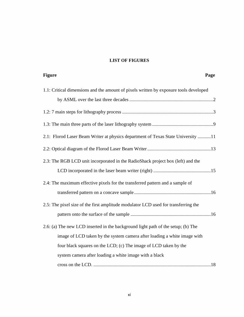
1.1: Critical dimensions and the amount of pixels written by exposure tools developed
by ASML over the last three decades ......................................................................2
1.2: 7 main steps for lithography process ............................................................................3
1.3: The main three parts of the laser lithography system ...................................................9
2.1: Florod Laser Beam Writer at physics department of Texas State University ...........11
2.2: Optical diagram of the Florod Laser Beam Writer .....................................................13
2.3: The RGB LCD unit incorporated in the RadioShack project box (left) and the
LCD incorporated in the laser beam writer (right) ................................................15
2.4: The maximum effective pixels for the transferred pattern and a sample of
transferred pattern on a concave sample ................................................................16
2.5: The pixel size of the first amplitude modulator LCD used for transferring the
pattern onto the surface of the sample ...................................................................16
2.6: (a) The new LCD inserted in the background light path of the setup; (b) The
image of LCD taken by the system camera after loading a white image with
four black squares on the LCD; (c) The image of LCD taken by the
system camera after loading a white image with a black
cross on the LCD. ..................................................................................................18
xii
2.7: z-stack of a convex sample, ∆z=1 μm (square size is 3x3 μm2 at sample
position, 50x objective) ..........................................................................................18
2.8: (a) Mirror1 transmittance, (b) Reflectance on surface B ............................................21
2.9: The new mirror1 transmittance and reflectance .........................................................22
2.10: (a) The mirror5 transmittance (b) Reflectance on surface A ....................................23
2.11: (a) The new mirror5 transmittance (b) Reflectance on surface A ............................24
2.12: Entrance pupil modification for SLM installation ....................................................26
3.1: a: PAN LC molecules’ alignment in the absence of electric field, b: PAN LC
molecules’ alignment after applying an electric field ............................................29
3.2: 7 major parts of each pixel on reflective LCOS SLMs...............................................30
3.3: Twisted nematic LCD .................................................................................................31
3.4: Holoeye Model-LC 2002 modulator (left) and optical image of pixel
array (right) ............................................................................................................34
3.5: Basic setup for LC 2002 SLM ....................................................................................34
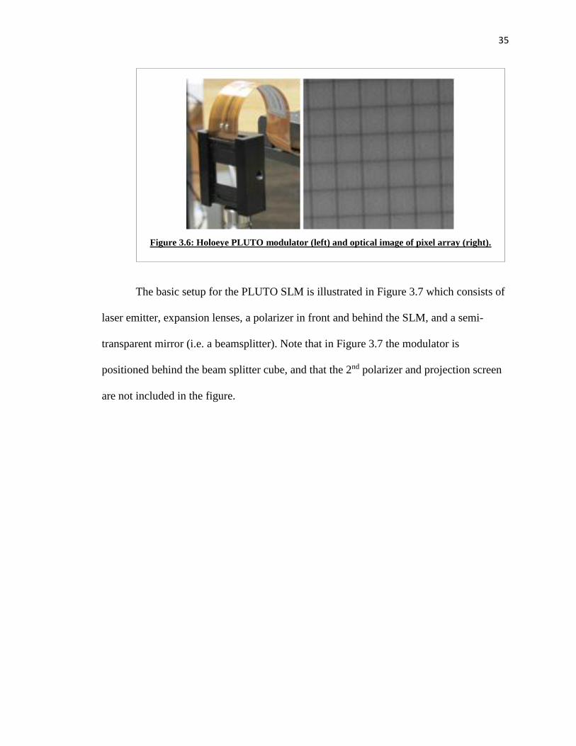
3.6: Holoeye PLUTO modulator (left) and optical image of pixel array (right) ...............35
3.7: Basic setup for PLUTO SLM .....................................................................................36
4.1. Depth of focus .............................................................................................................37
4.2. The image is in-focus on the tilted plane when dwsin(θ)<DOF .................................38
4.3. Some parts of image is out of focused on the tilted plane when dwsin(θ)>DOF .......38
4.4. System with two lenses with different focal lengths ..................................................39
4.5: Phase Image of the lens function with n0=255 and α= 0.00283 (f=87.06m
for LC-SLM at 532nm) ..........................................................................................44

xiii
4.6: Grayscale value along the x axis of the lens function with β=256 and
α= 0.00283 (f=87.06m for LC-SLM at 532nm) ....................................................45
4.7: Minimum focal length and the corresponding F/# of lenses implemented
in LC-2002 and Pluto as a function of the lens radius r.........................................46
4.8: Electronically controllable focal depth for the LC2002 and Pluto together
with the DOF of the 50x objective (50x objective, λ=532 nm) .............................48
4.9: Diffraction limited spot size of focused laser beam together with system
resolution without electronic focusing (50x objective, λ =532 nm) ......................49
4.10. The phase image of the lens function with β=255 and α= 0.01 (f=24.64 m
for the LC2002 at 532 nm).....................................................................................50
4.11: The grayscale value along the x axis of the lens function with β=255 and
α= 0.01 (f=24.64 m for the LC2002 at 532 nm) ....................................................51
4.12: (a) The ideal phase function and quantized and pixelated phase function;
(b) The effect of Quantization; (c) The effect of Pixelation; (d) total aberration ..52
4.13. The phase image of the lens function with β =255 and α= 0.55 (f=0.448m
for LC-SLM at 532nm) ..........................................................................................53
4.14: (a) Pixelation and (b) quantization aberration of the SLM lens of Fig. 3.1 ..............54
4.15: The phase function along x-axis for a Fresnel lens ..................................................56
4. 16: Focal length and F/# as a function of radius for a Fresnel lens implemented
in LC 2002 and Pluto .............................................................................................57
4.17. Percentage of the pixels vs. difference between calculated GV(x’,y’) value
and nearest integer for a lens with β = 255 and α = 0.01 (f=24.64m for
LC-SLM at 532nm)................................................................................................59
4.18. The P value for different α values from 0.1 to 0.3 (f=0.82m to 2.46m
xiv
for LC-SLM at 532nm) ..........................................................................................59
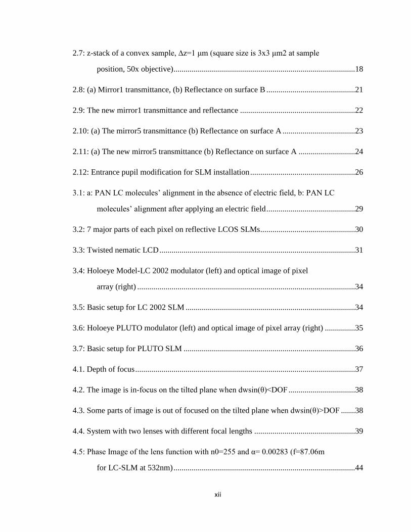
4.19. The average of the differences between GV of 100 points inside pixels
and the GV at center of that pixel for different α ...................................................60
4.20. Left lens α=0.1 and right lens α=0.12 .......................................................................61
4.21. Projection of two Texas Lone Stars on a perpendicular (a, b) and a tilted
surface (c) using dual lens phase function .............................................................62
4.22. Pixelation error for three different lens sizes ............................................................63
5.1: The diagram of an ordinary camera with three parallel planes ...................................66
5.2: The diagram of a tilted lens, Scheimpflug & Hinge principle ....................................66
5.3: The system setup to investigate the results of tilted lens function..............................68
5.4: Tilted sample (θ=1.76⁰), flat lens, 20x objective, 19.5x36.7 μm2, Z= 0μm ...............69
5.5: Tilted sample (θ=1.76⁰), flat lens, 20x objective, 19.5x36.7 μm2, Z= 11μm .............70
5.6: Tilted sample (θ=1.76 ⁰), tilted lens (θ=27.5 ⁰), 20x objective, 25x25 μm2
, Z= 0μm .................................................................................................................70
5.7: Tilted sample (θ=1.76 ⁰), tilted lens (θ=27.5 ⁰), 20x objective, 25x25 μm2
, Z= 3μm .................................................................................................................71
6.1: Diffraction between two parallel planes .....................................................................73
6.2: Diffraction geometry...................................................................................................74
6.3: Diffraction between two parallel planes .....................................................................77
6.4: Positioning a spherical lens with focal length f in front of the x-y plane to
ignore the phase factors .........................................................................................77
6.5: Modulating the phase instead of the amplitude using the SLM .................................79
xv
6.6: (a) The Bobcat logo Texas State University; (b) Old SWT logo; (c) Far field
diffraction pattern if one combines the amplitude of the other one .......................80
6.7: The effect of a lens on plane waves ............................................................................81
6.8: Gerchberg-Saxton algorithm diagram ........................................................................83
6.9: The simulation result of Gerchberg-Saxton algorithm ...............................................84
6.10: The diffraction between two non-parallel planes .....................................................85
6.11: The orientation of the planes for inverse diffraction ................................................86
6.12: The modified Gerchberg-Saxton algorithm diagram ................................................91
6.13: Simulation result of Modified Gerchberg Saxton algorithm ....................................92
6.14: Experimental result of Modified Gerchberg Saxton algorithm ................................93
xvi
ABSTRACT
DEVELOPMENT OF AN EXPOSURE TOOL FOR LITHOGRAPHY ON TILTED
AND CURVED SURFACES USING A SPATIAL LIGHT MODULATOR
by
Javad Rezanezhad Gatabi
Texas State University-San Marcos
December 2013
SUPERVISING PROFESSOR: Ir. Wilhelmus J. Geerts
This thesis is on research to develop a new laser lithography exposure tool for use on
non-flat substrates. Such a tool does currently not exists as commercial equipment used in
the electronic industry uses high numerical aperture (NA) lenses to create patterns with
critical dimensions down to 22 nm on very flat substrates (+/- 100 nm). The ability to
pattern thin films on top of curved substrates with large topography differences allows
for the development of new products and devices: it enable the integration of high density
integrated electronics on non planar samples such as those created by integrated optical,
micromechanical, and micromagnetic technologies, resulting in the realization of smart
sensors and actuators. The tool also opens up new opportunities in materials
characterization: the ability to place electric contacts on a 20 micron single crystalline
xvii
grain of a polycrystalline sample allow us to separate bulk and grain boundary
contributions to the electric transport properties of polycrystalline materials. An existing
Florod laser beam writer used for lithography on flat substrates was modified on three
different points to allow for the exposure of non-flat substrates: (1) The optical
throughput of the system wass optimized to allow for real-time determination of the
photoresist film thickness from the reflection spectrum of the sample; (2) A high
resolution optical light pattern generator was installed on the system and allows for the
determination of the sample’s topography by measuring the point spread functions and
the modulation transfer functions from the sample-microscopy system. The installed light
pattern generator is based on a Kopin high resolution amplitude spatial light modulator
(1.5 micron resolution on the sample) and a LED light source; (3) A Holoeye phase only
spatial light modulator (SLM) was installed on the system to allow for imaging on tilted
and curved substrates. Three different beam shaping methods were investigated: (1)
implementation of a single lens or multi-lens array on the SLM to allow for electronic
focus control across a curved or tilted sample. The controllable focus range is up to 16
mm for the Pluto modulator and up to 0.7 mm for the LC2002 modulator. For large single
SLM lenses the system is limited by aberrations caused by quantization, pixellation, and
curvature of the modulator. Implementation of an SLM multilens array whose lenses
have different focal distances increases the depth of field at the expense of a larger
diffraction limited spot size; (2) implementation of a tilted lens function in the SLM
allows for imaging on tilted samples. Preliminary experiments however show that the
imaging quality is limited when using the SLM lens in combination with a real object; (3)
implementation of the Gerchberg-Saxton algorithm to calculate the SLM optical field

xviii
required to generate a certain intensity pattern on a tilted sample. The classical
Gerchberg Saxton algorithm that was developed for Fraunhofer diffraction was adapted
for finite projection distances and tilted samples. The algorithm appears to be stable and
converging for the tested patterns and shows a light focussing improvement with respect
to the classical algorithm.
1
CHAPTER I: INTRODUCTION
This chapter provides a short introduction to lithography as used in the semiconductor
industry. The motivation for research and devlopement of a lithography exposure tool
that will enable nanostructuring of non flat samples is followed by a summary of the
work of others on this topic. In the second part of the chapter the modifications required
to a standard lithography exposure tool to make it suitable for lithography on 3D
substrates are described. The chapter finishes with how these modifications were
addressed in this thesis work.
Lithography
Lithography is an important step for the fabrication of electronic components. In
the lithography process, the blue-print of the circuit diagram is transferred onto the wafer
by nanopatterning conducting, semiconducting, and insulating thin films on top of the
wafer. Currently the photolithographic process steps can contribute up to 50% of the
wafer costs. In 2013 the most advanced lithography equipments were able to expose up
to 250 wafers per hour and write 2.6E12 pixels per field exposure (26x33 mm2). Note
that the number of pixels of a lithographic exposure tool is more than 6 orders of
magnitude larger than that of a professional DSLR camera lens. The following figure
shows the typical critical dimensions and the number of pixels written by a commercial
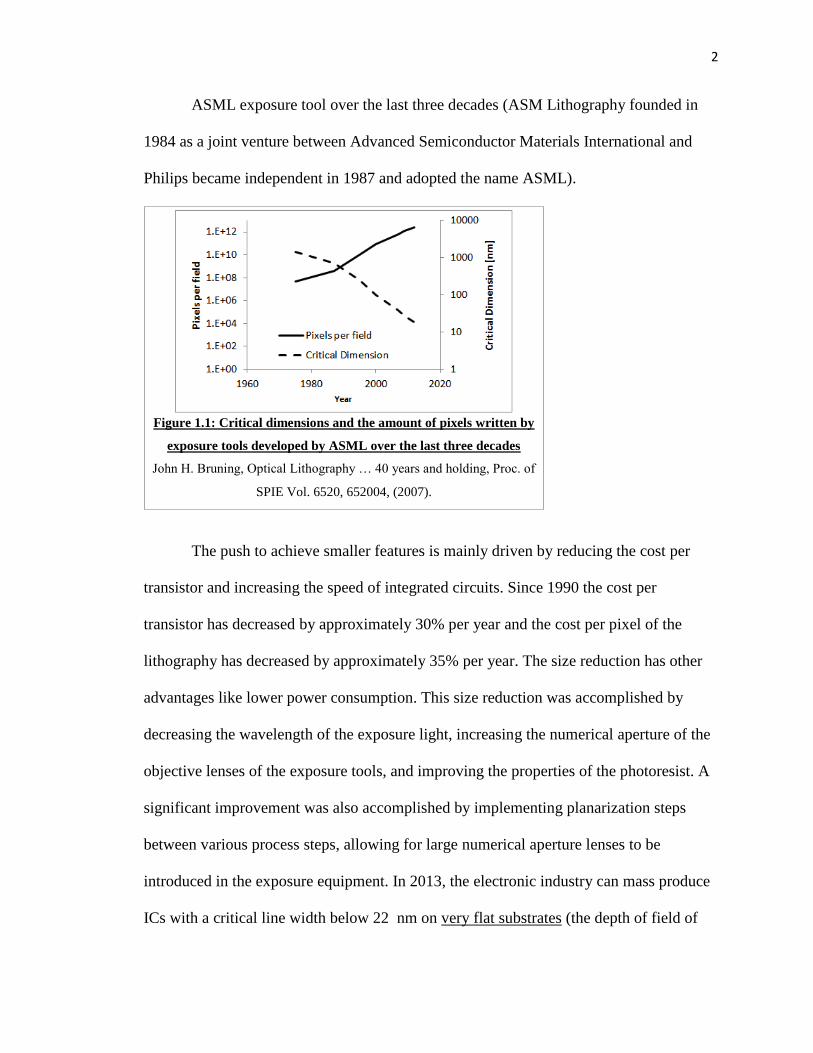
2
ASML exposure tool over the last three decades (ASM Lithography founded in
1984 as a joint venture between Advanced Semiconductor Materials International and
Philips became independent in 1987 and adopted the name ASML).
The push to achieve smaller features is mainly driven by reducing the cost per
transistor and increasing the speed of integrated circuits. Since 1990 the cost per
transistor has decreased by approximately 30% per year and the cost per pixel of the
lithography has decreased by approximately 35% per year. The size reduction has other
advantages like lower power consumption. This size reduction was accomplished by
decreasing the wavelength of the exposure light, increasing the numerical aperture of the
objective lenses of the exposure tools, and improving the properties of the photoresist. A
significant improvement was also accomplished by implementing planarization steps
between various process steps, allowing for large numerical aperture lenses to be
introduced in the exposure equipment. In 2013, the electronic industry can mass produce
ICs with a critical line width below 22 nm on very flat substrates (the depth of field of
Figure 1.1: Critical dimensions and the amount of pixels written by
exposure tools developed by ASML over the last three decades
John H. Bruning, Optical Lithography … 40 years and holding, Proc. of
SPIE Vol. 6520, 652004, (2007).
3
the 22 nm node is around 200 nm). Memories with 22 nm features were first
commercially produced in 2008 and since 2012, microprocessors are also made with
features that small. The research community is currently working on finding solutions to
create electronics with 14 nm critical dimensions. Various methods such as extreme UV
(EUV) and Electron Beam lithography are investigated to mass fabricate ICs with
features below 22 nm.
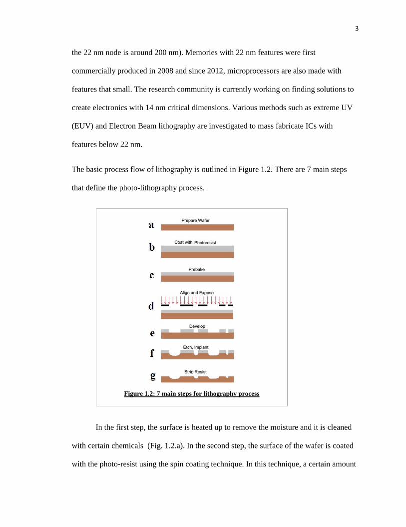
The basic process flow of lithography is outlined in Figure 1.2. There are 7 main steps
that define the photo-lithography process.
In the first step, the surface is heated up to remove the moisture and it is cleaned
with certain chemicals (Fig. 1.2.a). In the second step, the surface of the wafer is coated
with the photo-resist using the spin coating technique. In this technique, a certain amount
Figure 1.2: 7 main steps for lithography process
4
of photo-resist material is dispenced on the surface and the wafer is spun with a high
rotational velocity. In this way, a uniform thin layer of photoresist covers the surface
(Fig. 1.2.b). Important parameters of the spinning process that define the photoresist
thickness are angular acceleration, final spin speed and the total duration of the spin
process. The thickness of the photoresist layer also depends on the viscosity of the
photoresist as well as the exhaust connected to the spinner. The angular acceleration
mainly influences the homogeneity of the layer across the wafer surface. In case of non-
rotation-symmetric substrates, the resist forms a pronounced edge bead near the substrate
edges due to the strong air turbulences. After spinning, the wafer is prebaked to remove
the photoresist solvent and make the sample less sticky (Fig. 1.2.c). It is important to
keep the parameters of the spining and pre-bake constant as both have a strong influence
on the photoresist film thickness. A reproducable thermal contact between the wafer and
the hot plate during the pre-bake by means of a vacuum chuck is essential to create a
consistent photoresist film thickness across a sample series. In the fourth step, the mask
containing the blue print of the microstructuring is aligned, followed by the
exposure.(Fig. 1.2.d). Exposing the photoresist material by a light beam causes a
chemical change in the photoresit material; for positive (negative) photoresists, the
exposed (unexposed) regions are soluble in the developer, creating windows in the
photoresist layer. (Fig. 1.2.e). The exposed surface of the wafer is then etched by
chemicals (wet etch) or by a plasma (dry etch) (Fig. 1.2.f) creating the desired
microstructure on the wafer. The remaining photoresist material is then removed using
wet chemicals or using a plasma containing oxygen (Fig. 1.2.g).

5
The mask to create the desired pattern determines the the resolution and quality of
the product and it is a costly part of the lithography process. In mass production, it is
reasonable to use expensive masks. However, in prototyping, it is not reasonable to spend
lots of money to fabricate a mask which is used only for making several samples. Hence,
using a focussed laser beam writer and directly writing the pattern onto the photoresist is
an economical alternative used for rapid prototyping or when producing ICs with small
production volumes. Recently, researchers have accomplished optical beam lithography
creating 9 nm features [1] which is approaching the capabilities of electron beam
lithography, an expensive alternative. The disadvantage of maskless lithography is the
slow throughput related to the serial character of the writing process: The pattern is
written one pixel at a time. To ameliorate this issue, researchers have recently started to
incorporate digital mirror arrays [2] and phase plates [3] into the exposure equipment,
writing millions of pixels simultaneously. Although those fast maskless lithography
exposure tools are very popular for the mass production of printed circuit boards, they
still seem to lack the high resolution of conventional exposure tools which use masks.
Note that since the seventies above mentioned direct write approaches are also used for
making the masks.
Lithography on Non-flat Substrates.
All commercial exposure tools are meant to be used on flat substrates. In fact part
of the resolution improvements of lithography exposure tools have been realized by the
introduction of higher NA lenses and more homogeneous illumination devices (NA of 22
6
nm node is 1.35). These improvements require flatter samples. Lithography exposure
equipment that can provide us with a mean to create nano-structures on non-flat samples
would result in new research and development opportunities and possibly new products.
Such tool could for example be used to integrate electronics on devices created with non-
flat technologies such as multi-lens arrays, electro-optical devices, magnetic sensors and
actuators, or micro-mechanical devices. Integration of all those non flat technologies with
electronics allows for the development of new novel smart and fast devices. It is expected
that a lithography exposure tool for non-flat substrates would also create new
measurement strategies in materials research. For example such tool would allow us to
put contacts on a 20 um single crystalline grain for electrical characterization resulting in
a measurement method to separate the contributions of defect and grain boundary
scattering to the resistivity of poly crystalline materials.
Current research and applications of lithography on non-flat substrates are scarce.
Ball Semiconductor has developed special equipment for lithography on 1 mm diameter
silicon spheres for novel electronic devices, including microwave and solar cell
applications. Since the total surface area of a sphere is about 3 times larger than the area
of a flat substrate this approach can reduce the associated cost. Other advantages of their
technology are the capability to realize high inductors on the spheres, and the option to
create 3D devices such as 3D CCD camera and 3D accelerometers. Their lithography
system uses six digital micro mirror devices (DMD) each of which consists of an array of
800x600 micro-mirrors and functions as an electronic mask. Each DMD is projected by a
micro lens system on a part of the sphere. Six of these devices approximately cover the
complete sphere. Although ingenious, their setup can only work for spheres with a
7
diameter of around 1 mm [4]. Several researchers used projection lithography to create
structures on cylindrical surfaces [5, 6], and on curved surfaces of revolution used for
MEMS or integrated optics applications [7]. Other technologies, such as nanoimprint,
have been used on concave or convex lens surfaces [8, 9], and on cylindrical surface [10,
11]. Direct electron beam lithography has been applied to create aspheric lenses on
concave mirror surfaces [12]. To keep the electron beam focused on all positions on the
substrate and to keep the electron dose constant, the electron beam was placed at a
working distance that is equal to the radius of curvature of the sample. An extensive
literature search found only a handful of research groups that are using a laser beam
writer for lithography on simple non-flat substrates [13, 14, 15]. Radtke et al. use a
modified DWL400 laser beam writer [15]. They extended the instrument with a tilting
stage that can tilt the sample +/- 10o along two orthogonal axes, allowing direct writing
on concave and convex surfaces [15]. Snow et al. incorporated a rotary stage in a
conventional laser beam writer setup. This enables writing on a set of aligned cylindrical
glass fibers [14]. Their paper discusses the effect of substrate curvature on the delivered
exposure dose. Zhang et al. use a traditional laser beam writer with XY-control of the
substrate and z-control of the objective to write a grating on convex lens surfaces [13].
Before starting with the writing process, they center the laser beam in the middle of the
lens. Next, in order to keep the laser beam more-or-less focused on the surface during the
writing process, they use an algorithm that simultaneously scans in the X and Z
directions. Their system does not make automatic corrections of the exposure dose, or the
line width of the sloped parts of the substrate. Hence, they can only produce uniform
gratings on simple, weakly curved, non-flat substrates. Recently, Chen et al. presented a
8
new mathematical model of the optical field distribution when exposing photoresist
material on convex substrates [16]. Romero et al. used a laser beam writer to create a
multi lens array on a curved surface [17]. In both of these works, the photoresist layer on
the substrate surface with known curvature is also exposed by a laser beam.
Lithography on non-flat substrates is not trivial for several reasons. Spinning can no
longer be used to apply photoresist to non-flat samples and one should use other methods
such as for example an air-brush, high pressure evaporation, or a simple eye-dropper.
Also the exposure tool need to be adapted since because of the non-linear chemical
response of photoresist to the exposed light intensity, the laser beam intensity should be
adjusted on curved surfaces or in areas that have a different photoresist film thickness.
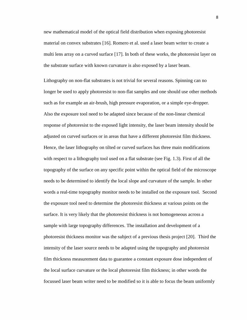
Hence, the laser lithography on tilted or curved surfaces has three main modifications
with respect to a lithography tool used on a flat substrate (see Fig. 1.3). First of all the
topography of the surface on any specific point within the optical field of the microscope
needs to be determined to identify the local slope and curvature of the sample. In other
words a real-time topography monitor needs to be installed on the exposure tool. Second
the exposure tool need to determine the photoresist thickness at various points on the
surface. It is very likely that the photoresist thickness is not homogeneous across a
sample with large topography differences. The installation and development of a
photoresist thickness monitor was the subject of a previous thesis project [20]. Third the
intensity of the laser source needs to be adapted using the topography and photoresist
film thickness measurement data to guarantee a constant exposure dose independent of
the local surface curvature or the local photoresist film thickness; in other words the
focussed laser beam writer need to be modified so it is able to focus the beam uniformly
9
on a tilted or curved. Although this thesis work has mainly focussed on the last problem,
i.e. shaping the laser beam and wrapping the 2D blue-print around a 3D surface, two
significant contributions were made in support of the first two required modifications: (1)
New hardware, software and optics was developed and integrated in the system to allow
for topography measurements [18,19]; (2) The optical throughput of the alignment beam
was increased to improve the performance of the photoresist thickness monitor and allow
for faster photoresist film thickness measurements [20]. Both modifications are described
in chapter 2 while the rest of the thesis focusses on the laser beam shaping part of the
project using a phase only spatial light modulator (SLM). Three different methods were
explored for beam shaping: (a) the SLM was used to implement an array of multi-lenses
each with their own focal distance imaging a different part of the mask (chapter IV); (b)
the SLM was used to implement a titled lens which allows for imaging on a tilted surface
similar to the tilt and shift lenses that are used by professional photographers (chapter V);
(c) the SLM was used to implement a modified version of the Gerchberg-Saxton
algorithm to allow for the calculation of the SLM’s optical field for the projection on a
tilted surface (chapter VI).
Figure 1.3: The main three parts of the laser lithography
system: (a) beam shaping unit; (b) topography monitor; (c)
photoresist film thickness monitor.
10
CHAPTER II: LASER BEAM SETUP
This chapter introduces the Florod laser beam system that was used for experiments. The
Florod laser beam writer is originally designed for lithography on non-flat substrates. To
prepare the system for the present study, some modifications were done on the Florod
laser beam writer. These modifications consist of: upgrading the optical elements to use a
shorter wavelength laser and preparing the system for faster photoresist film thickness
monitoring, installing new hardware and optical components in support of the topography
measurement unit, and installing the SLM setup. In this chapter, first, the system
specifications are outlined and then the modifications made to the system are reported.
Florod Laser Beam Writer
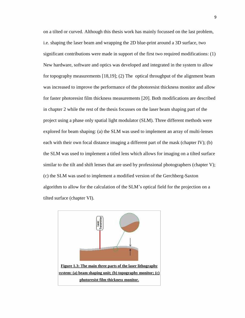
In this research, a Florod Laser Beam Writer as shown in Figure 2.1, is modified
for laser lithography on curved surfaces at the physics department of Texas State
University. The device was manufactured by the Florod Corporation and was designed to
be used with an argon laser working in the wavelength range of 454nm-514nm.
11
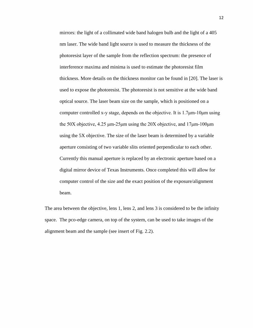
Figure 2.2 shows the optical diagram of the Florod Laser Beam Writer. The
design is based on an infinity corrected optical microscope and uses Mitutoyo long
distance objectives. The system consists of three different parts:
(a) The imaging column (see left Fig. 2.2.) consisting of the sample, the objective, the
tube lens (lens 2), and a fast and sensitive camera (pco.edge). The tube lens has a
focal distance of 120 mm resulting in a magnification of 30x for a 50x objective.
(b) The background light column consisting of a light source, a compound lens (lens
1), the objective and the sample. This path is designed for the background light
which keeps the whole sample visible under the microscope.
(c) The exposure/alignment column consisting of two light sources, an aperture, the
laser beam lens (lens 3), the objective, and the sample. This light path is meant to
create and a focused laser beam that is used to exposure the photoresist and a
focused white light beam that is used to measure the thickness of the photoresist
layer. Two light beams are coupled into the system using semi-transparent
Figure 2.1: Florod Laser Beam Writer at the physics department of Texas
State University
12
mirrors: the light of a collimated wide band halogen bulb and the light of a 405
nm laser. The wide band light source is used to measure the thickness of the
photoresist layer of the sample from the reflection spectrum: the presence of
interference maxima and minima is used to estimate the photoresist film
thickness. More details on the thickness monitor can be found in [20]. The laser is
used to expose the photoresist. The photoresist is not sensitive at the wide band
optical source. The laser beam size on the sample, which is positioned on a
computer controlled x-y stage, depends on the objective. It is 1.7μm-10μm using
the 50X objective, 4.25 μm-25μm using the 20X objective, and 17μm-100μm
using the 5X objective. The size of the laser beam is determined by a variable
aperture consisting of two variable slits oriented perpendicular to each other.
Currently this manual aperture is replaced by an electronic aperture based on a
digital mirror device of Texas Instruments. Once completed this will allow for
computer control of the size and the exact position of the exposure/alignment
beam.
The area between the objective, lens 1, lens 2, and lens 3 is considered to be the infinity
space. The pco-edge camera, on top of the system, can be used to take images of the
alignment beam and the sample (see insert of Fig. 2.2).
13
Figure 2.2: Optical diagram of the Florod Laser Beam Writer
The insert shows a picture taken with the system’s camera from an electronic circuit positioned on
the stage. The square in the middle of the image is the alignment beam.
14
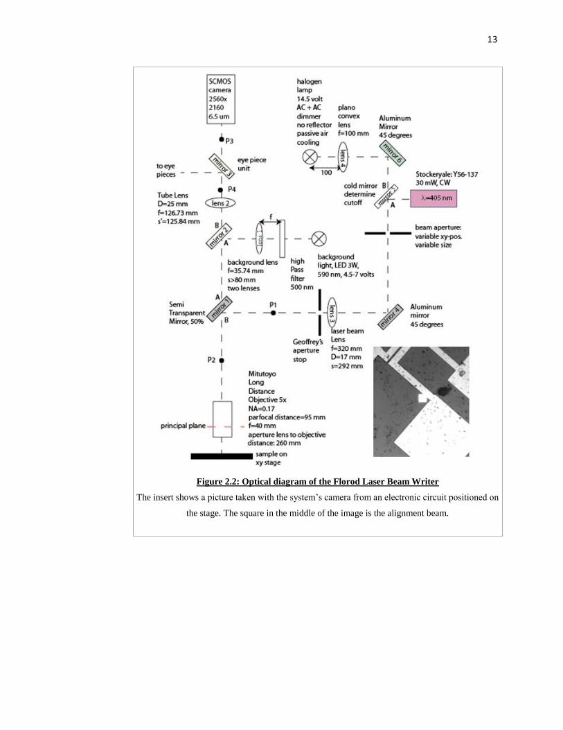
Modifications for Topography Monitor
To measure the surface topography of the sample a light pattern generator was
installed in the background light optical beam of the setup. This generator allows for the
projection of a specific light pattern onto the sample. The optical response of the system
is measured by taking images of the projected light pattern on the sample using the CCD
camera installed on the system. As the optical response of the system depends on the
sample slope and the out of focus error, it is possible to determine the sample topography
from those measurements. Typical test patterns are arrays of delta-functions and periodic
gratings. The former allows for the determination of the point spread functions while the
latter allows for the determination of the modulation transfer function of the sample-
microscope system. [18, 19].
To generate the pattern for topography measurements several options were
considered, i.e. a permanent mask, a 3D mask consisting of a stack of microscope slides
each containing a mask, and an electronic mask. To get as much flexibility as possible the
latter option was implemented. An amplitude modulator LCD was placed in the
background light optical beam at the focal point of lens1 (see Fig. 2.3). To reduce the
heat load of the light source on the LCD the original halogen background light bulb was
replaced by a 3Watt/12 volt commercial automobile LED bulb (Super Bright LEDs).
Experiments were performed with three different colors, i.e. orange (1156-ALX3: 590
nm)), red (1156-RLX3: 617 nm), and white (WLX3). The AC-power supply of the light
source was replaced with a DC lab supply. For the electronic mask preliminary
experiments were performed with an RGB LCD that was pulled out from a working
projector ($100- Shift 3 Lightblast Entertainment Projector from CVS Pharmacy). This
15
LCD had a pixel size of 126 x 63 um and used a standard video input. The control
electronics and its power supply were also removed from the projector and incorporated
in a RadioShack project box (see Fig. 2.3 a). The Radio-Shack box was mounted on a
manual xy-stage and then incorporated in the system (see Fig. 2.3b). The LCD was
controlled via a video-card in the back of the computer.
Figure 2.4 shows an image taken with the system camera after installing the LCD
in the background light column. The effective pixels for the transferred pattern are
limited to 8X12 pixels because of the spherical aberration of lens 1 (Fig. 2.2) and the
large pixel size of the LCD. Figure 2.4a shows an image taken with the system camera
when a flat sample is positioned on the xy-stage and a grating pattern is loaded on the
LCD. In between the grating lines, the individual LCD pixels are visible. As this LCD
has the red, green, and blue color filters integrated in each consecutive pixel, the pixels
showed up with different grey scale values on the monochrome CCD image. Figure 2.4b
shows an image taken with the system camera when a concave sample is positioned on
the xy-stage and a white image is loaded on the LCD. It is clear that only the pixels in a
ring are focused while the pixels at the center of the image are out of focus. It is also clear
Figure 2.3: The RGB LCD unit incorporated in the RadioShack project box (left) and the LCD
incorporated in the laser beam writer (right)
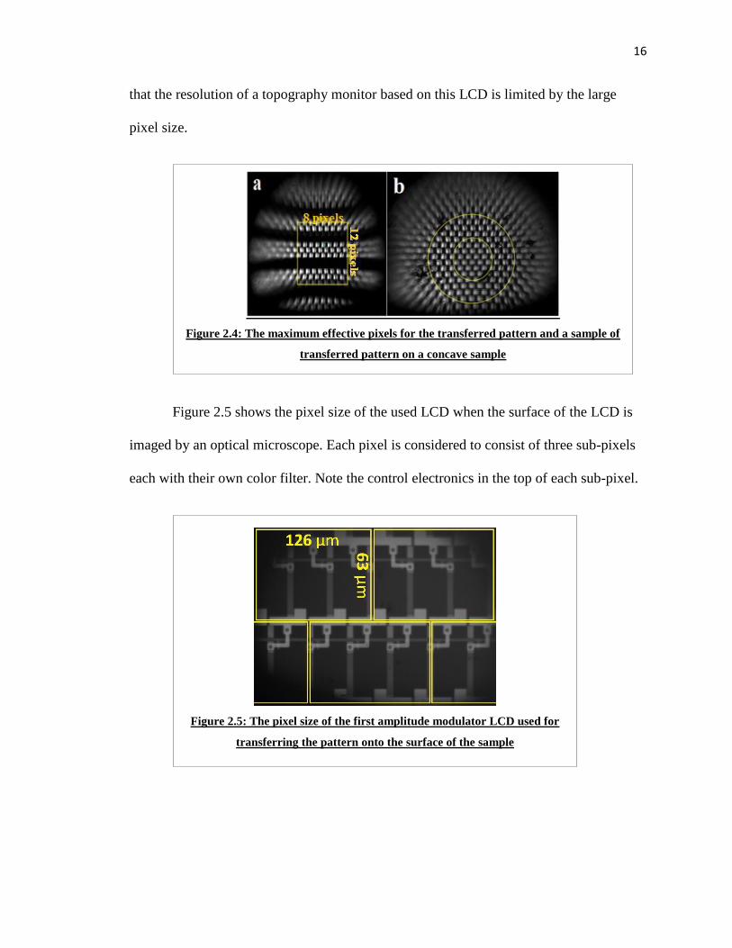
16
that the resolution of a topography monitor based on this LCD is limited by the large
pixel size.
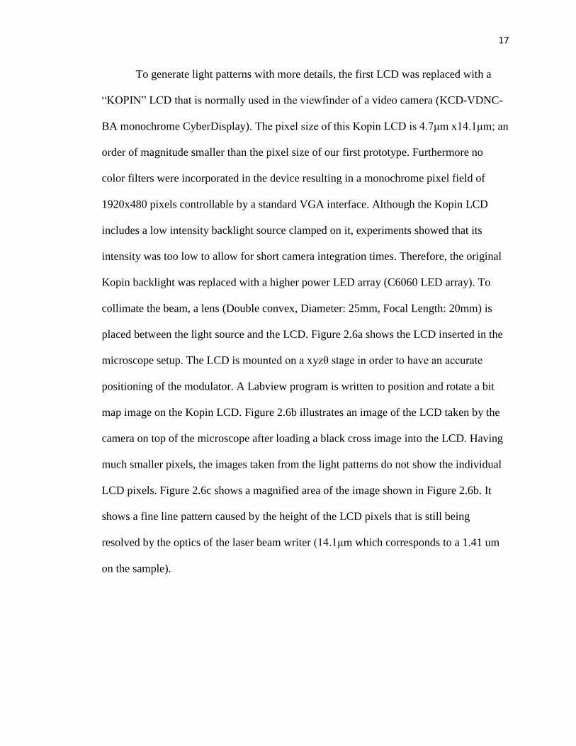
Figure 2.5 shows the pixel size of the used LCD when the surface of the LCD is
imaged by an optical microscope. Each pixel is considered to consist of three sub-pixels
each with their own color filter. Note the control electronics in the top of each sub-pixel.
Figure 2.5: The pixel size of the first amplitude modulator LCD used for
transferring the pattern onto the surface of the sample
Figure 2.4: The maximum effective pixels for the transferred pattern and a sample of
transferred pattern on a concave sample
17
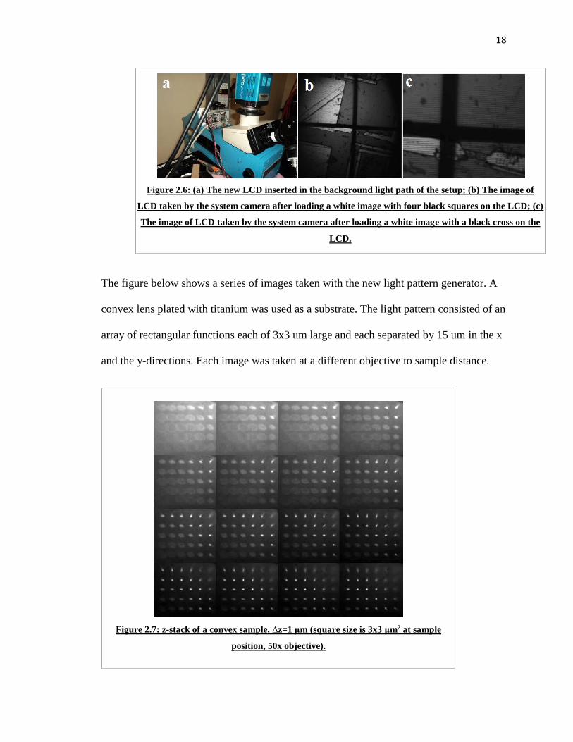
To generate light patterns with more details, the first LCD was replaced with a
“KOPIN” LCD that is normally used in the viewfinder of a video camera (KCD-VDNC-
BA monochrome CyberDisplay). The pixel size of this Kopin LCD is 4.7μm x14.1μm; an
order of magnitude smaller than the pixel size of our first prototype. Furthermore no
color filters were incorporated in the device resulting in a monochrome pixel field of
1920x480 pixels controllable by a standard VGA interface. Although the Kopin LCD
includes a low intensity backlight source clamped on it, experiments showed that its
intensity was too low to allow for short camera integration times. Therefore, the original
Kopin backlight was replaced with a higher power LED array (C6060 LED array). To
collimate the beam, a lens (Double convex, Diameter: 25mm, Focal Length: 20mm) is
placed between the light source and the LCD. Figure 2.6a shows the LCD inserted in the
microscope setup. The LCD is mounted on a xyzθ stage in order to have an accurate
positioning of the modulator. A Labview program is written to position and rotate a bit
map image on the Kopin LCD. Figure 2.6b illustrates an image of the LCD taken by the
camera on top of the microscope after loading a black cross image into the LCD. Having
much smaller pixels, the images taken from the light patterns do not show the individual
LCD pixels. Figure 2.6c shows a magnified area of the image shown in Figure 2.6b. It
shows a fine line pattern caused by the height of the LCD pixels that is still being
resolved by the optics of the laser beam writer (14.1μm which corresponds to a 1.41 um
on the sample).
18
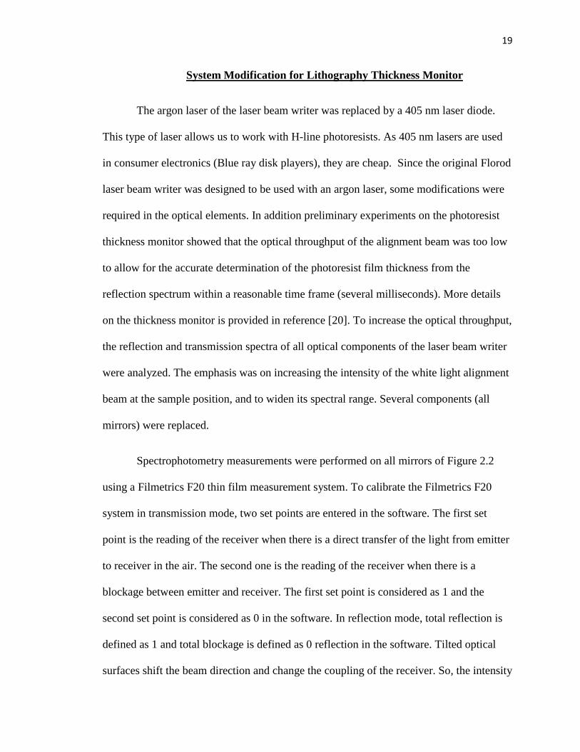
The figure below shows a series of images taken with the new light pattern generator. A
convex lens plated with titanium was used as a substrate. The light pattern consisted of an
array of rectangular functions each of 3x3 um large and each separated by 15 um in the x
and the y-directions. Each image was taken at a different objective to sample distance.
Figure 2.7: z-stack of a convex sample, ∆z=1 μm (square size is 3x3 μm2 at sample
position, 50x objective).
Figure 2.6: (a) The new LCD inserted in the background light path of the setup; (b) The image of
LCD taken by the system camera after loading a white image with four black squares on the LCD; (c)
The image of LCD taken by the system camera after loading a white image with a black cross on the
LCD.
19
System Modification for Lithography Thickness Monitor
The argon laser of the laser beam writer was replaced by a 405 nm laser diode.
This type of laser allows us to work with H-line photoresists. As 405 nm lasers are used
in consumer electronics (Blue ray disk players), they are cheap. Since the original Florod
laser beam writer was designed to be used with an argon laser, some modifications were
required in the optical elements. In addition preliminary experiments on the photoresist
thickness monitor showed that the optical throughput of the alignment beam was too low
to allow for the accurate determination of the photoresist film thickness from the
reflection spectrum within a reasonable time frame (several milliseconds). More details
on the thickness monitor is provided in reference [20]. To increase the optical throughput,
the reflection and transmission spectra of all optical components of the laser beam writer
were analyzed. The emphasis was on increasing the intensity of the white light alignment
beam at the sample position, and to widen its spectral range. Several components (all
mirrors) were replaced.
Spectrophotometry measurements were performed on all mirrors of Figure 2.2
using a Filmetrics F20 thin film measurement system. To calibrate the Filmetrics F20
system in transmission mode, two set points are entered in the software. The first set
point is the reading of the receiver when there is a direct transfer of the light from emitter
to receiver in the air. The second one is the reading of the receiver when there is a
blockage between emitter and receiver. The first set point is considered as 1 and the
second set point is considered as 0 in the software. In reflection mode, total reflection is
defined as 1 and total blockage is defined as 0 reflection in the software. Tilted optical
surfaces shift the beam direction and change the coupling of the receiver. So, the intensity

20
of the received beam may be higher than the maximum intensity found during the
calibration procedure. In addition any small curvatures of the optical surfaces may also
influence the coupling transmitter and receiver. Hence, in the F20 measurement results
there are transmission or reflection values larger than 1, which of course have no physical
meaning. For our purpose, it is only important to determine the shape of the reflection
and transmission spectra. So, the variation of the transmission or reflection curves is
more important than their absolute values.
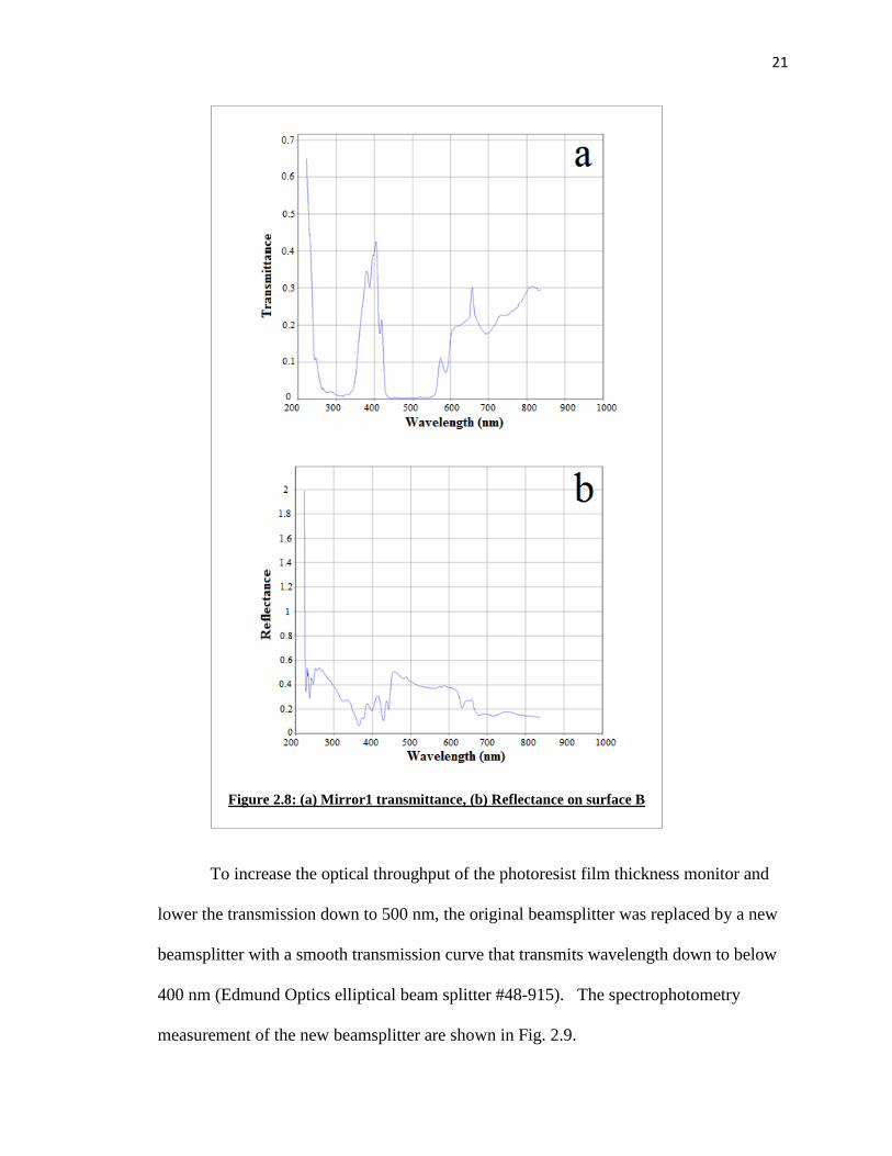
The transmission and reflection spectra for mirror1 are shown in Figure 2.8. The
data shows that mirror1 in transmittance mode works as a band-pass filter and has a
transmission curve with a lot of structures. This filter in the original design of the
machine is designed to block the laser beam to expose the eyepieces and camera. Because
the laser alignment lamp (halogen lamp) is used during spectrophotometry for photoresist
thickness measurement, this band-pass filter is not suitable in the new design of the
system.
21
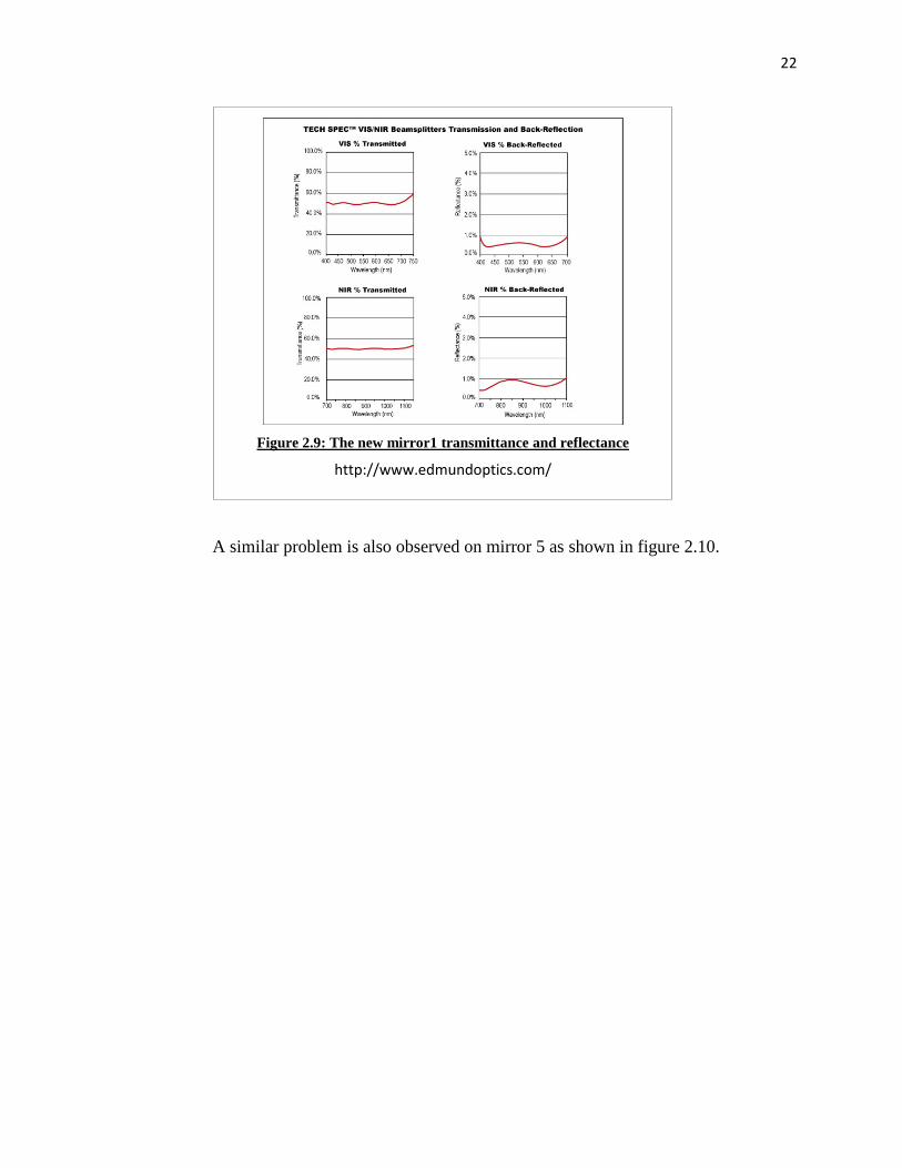
To increase the optical throughput of the photoresist film thickness monitor and
lower the transmission down to 500 nm, the original beamsplitter was replaced by a new
beamsplitter with a smooth transmission curve that transmits wavelength down to below
400 nm (Edmund Optics elliptical beam splitter #48-915). The spectrophotometry
measurement of the new beamsplitter are shown in Fig. 2.9.
Figure 2.8: (a) Mirror1 transmittance, (b) Reflectance on surface B
22
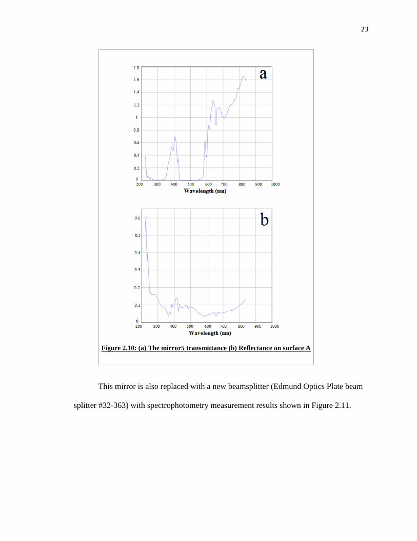
A similar problem is also observed on mirror 5 as shown in figure 2.10.
Figure 2.9: The new mirror1 transmittance and reflectance
http://www.edmundoptics.com/
23
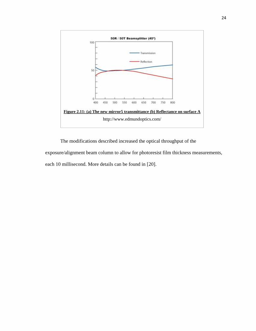
This mirror is also replaced with a new beamsplitter (Edmund Optics Plate beam
splitter #32-363) with spectrophotometry measurement results shown in Figure 2.11.
Figure 2.10: (a) The mirror5 transmittance (b) Reflectance on surface A
24
The modifications described increased the optical throughput of the
exposure/alignment beam column to allow for photoresist film thickness measurements,
each 10 millisecond. More details can be found in [20].
Figure 2.11: (a) The new mirror5 transmittance (b) Reflectance on surface A
http://www.edmundoptics.com/

25
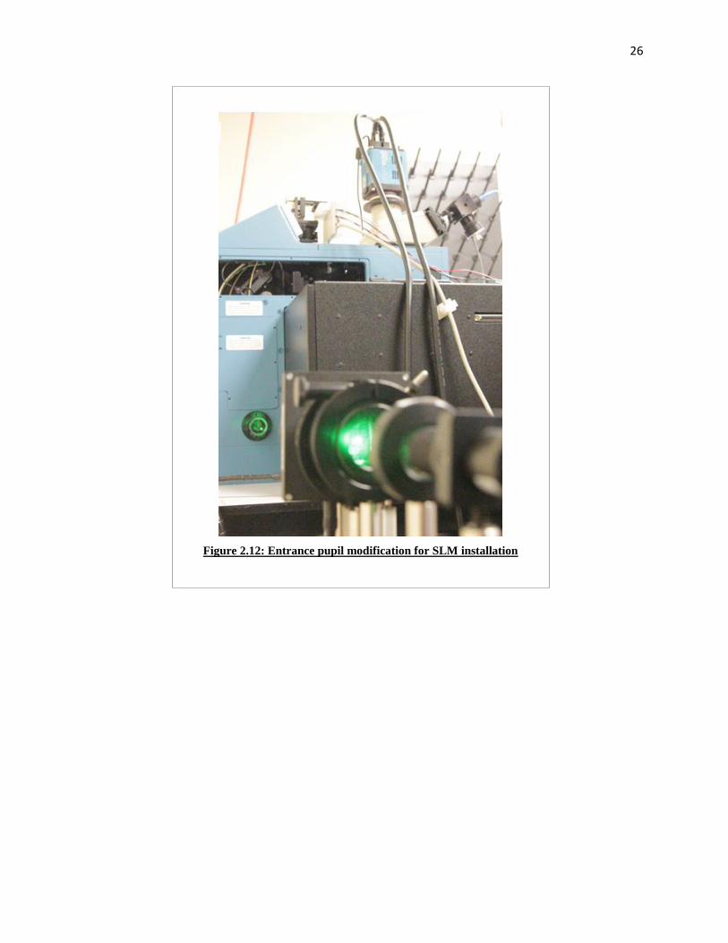
SLM Installation
The spatial light modulator was coupled into the system via the alignment beam
optical port of the system. To do this, lens 4 and the halogen lamp were temporarily
removed and the SLM setup was installed on a stand outside the machine (Figure 2.12).
Although, eventually the SLM needs to be coupled into the exposure/alignment beam via
mirror 5, this approach gave us more flexibility and space.
The laser beam after being modified by the SLM passes through the entrance
pupil of the laser beam writer. An intermediate image is formed at the position of the
beam aperture. This intermediate image is focused on the sample by the laser beam lens
(lens 3) and the objective.
26
Figure 2.12: Entrance pupil modification for SLM installation
27
CHAPTER III: SPATIAL LIGHT MODULATOR
Three different techniques are presented in this thesis to shape the laser beam on a
tilted or curved surface. All techniques are implemented on a phase Spatial Light
Modulator (SLM). This chapter describes primary parameters of SLMs as the main
device used in this research for the beam shaping. Two SLMs used in this study, the
Holoeye-PLUTO and Holoeye-LC2002, are described. The chapter also contains
descriptions of the setups used to test these two SLMs, one working in transmittance
mode and the other working in reflective mode.
Spatial Light Modulator Basics
A Spatial Light Modulator (SLM) is a device that is capable of spatially
manipulating the phase, amplitude, or polarization of a light beam. Each SLM device
contains a matrix of pixels that each can be addressed via the interface electronics of the
SLM. The phase shift, transmission, or polarization of each pixel can be independently
controlled optically or electronically often via a graphics interface card in a computer.
SLMs with different modulation mechanisms exist such as mechanical, magneto-opical
[21], electro-optical, and thermal [22]. The modulation mechanism deals with an
intermediate representation of information that interacts with the modulating medium
28
[23]. The modulators used for the work presented in this thesis are of the third type, so
called Liquid Crystal SLM (LC-SLM). Three types of LC-SLMs are on the market:
Twisted Nematic (TN) SLMs in which the orientation of the LC molecules differs
between the entrance and the exit window of the cell in a helix-like structure, Parallel
Aligned Nematic (PAN) SLMs in which the alignment of liquid crystals is parallel to the
substrate, and Vertical Aligned Nematic (VAN) SLMs in which the alignment of liquid
crystals is perpendicular to substrate [24].
Spatial light modulators can be fabricated based on translucent (LCD) or
reflective (liquid crystal on silicon: LCOS) technology. In transmissive PAN LCDs, a
conductive transparent oxide layer (often Indium Tin Oxide, i.e. ITO) and a light
modulator material (Liquid Crystals) are sandwiched between two glass substrate layers.
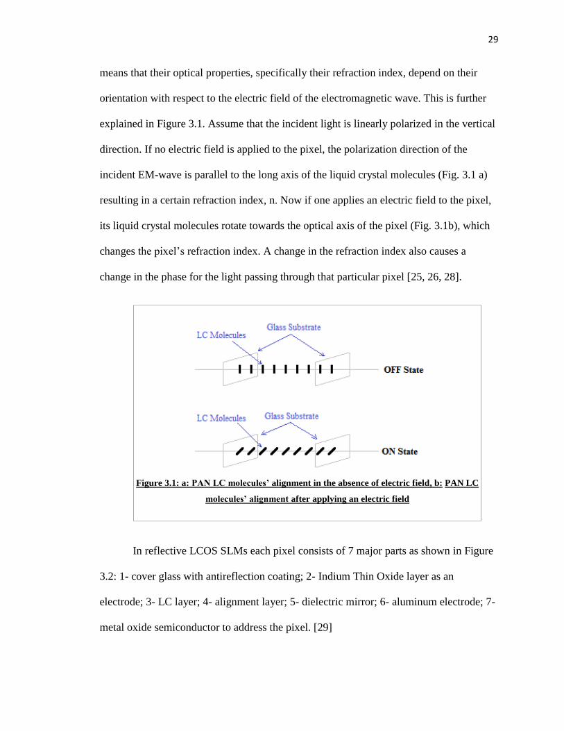
A liquid crystal consist of rod-like molecules that are long and rigid and have a
permanent electric dipole moment. These molecules have a tendency to orient themselves
in the same direction, called the director, and to line themselves up along micro-scratches
in a rubbed glass plate. Because of their electric dipole moment liquid crystal molecules
can be oriented by an externally applied electric field. Such electric field can be applied
to the liquid crystal molecules by applying an electric potential across the ITO electrodes
of each SLM pixel. In the absence of this electric field, the LC molecules’ alignment is
parallel to the glass substrates, parallel to the scratches in the rubbed glass substrates (Fig.
3.1a). After applying an electric field to the molecules, they tilt towards the optical axis
of the SLM while keeping their parallel alignment with respect to each other as shown in
figure 3.1b. So the orientation of the LC molecules in a certain pixel can be changed by
applying an electric field to a pixel. The liquid crystal molecules are birefringent. This
29
means that their optical properties, specifically their refraction index, depend on their
orientation with respect to the electric field of the electromagnetic wave. This is further
explained in Figure 3.1. Assume that the incident light is linearly polarized in the vertical
direction. If no electric field is applied to the pixel, the polarization direction of the
incident EM-wave is parallel to the long axis of the liquid crystal molecules (Fig. 3.1 a)
resulting in a certain refraction index, n. Now if one applies an electric field to the pixel,
its liquid crystal molecules rotate towards the optical axis of the pixel (Fig. 3.1b), which
changes the pixel’s refraction index. A change in the refraction index also causes a
change in the phase for the light passing through that particular pixel [25, 26, 28].
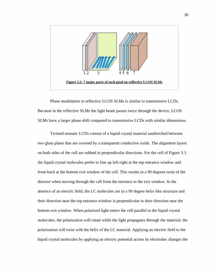
In reflective LCOS SLMs each pixel consists of 7 major parts as shown in Figure
3.2: 1- cover glass with antireflection coating; 2- Indium Thin Oxide layer as an
electrode; 3- LC layer; 4- alignment layer; 5- dielectric mirror; 6- aluminum electrode; 7-
metal oxide semiconductor to address the pixel. [29]
Figure 3.1: a: PAN LC molecules’ alignment in the absence of electric field, b: PAN LC
molecules’ alignment after applying an electric field
30
Phase modulation in reflective LCOS SLMs is similar to transmissive LCDs.
Because in the reflective SLMs the light beam passes twice through the device, LCOS
SLMs have a larger phase shift compared to transmissive LCDs with similar dimensions.
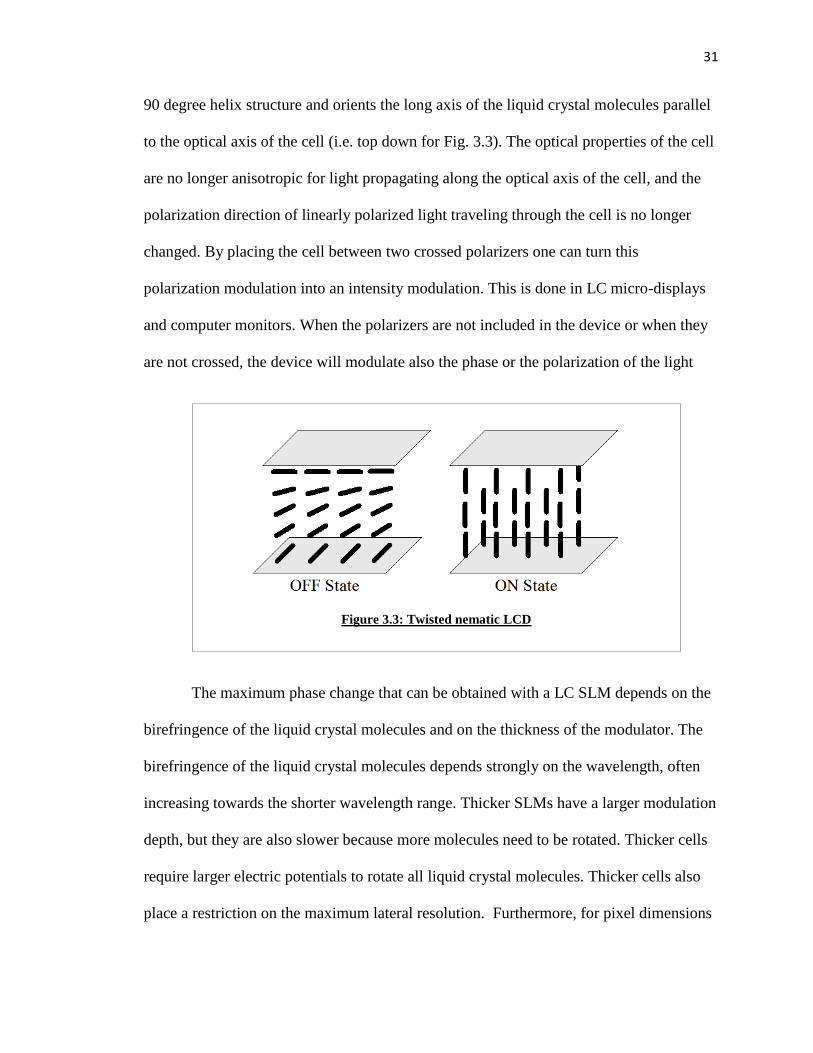
Twisted nematic LCDs consist of a liquid crystal material sandwiched between
two glass plates that are covered by a transparent conductive oxide. The alignment layers
on both sides of the cell are rubbed in perpendicular directions. For the cell of Figure 3.3
the liquid crystal molecules prefer to line up left-right at the top entrance window and
front-back at the bottom exit window of the cell. This results in a 90 degrees twist of the
director when moving through the cell from the entrance to the exit window. In the
absence of an electric field, the LC molecules are in a 90 degree helix-like structure and
their direction near the top entrance window is perpendicular to their direction near the
bottom exit window. When polarized light enters the cell parallel to the liquid crystal
molecules, the polarization will rotate while the light propagates through the material; the
polarization will twist with the helix of the LC material. Applying an electric field to the
liquid crystal molecules by applying an electric potential across its electrodes changes the
Figure 3.2: 7 major parts of each pixel on reflective LCOS SLMs
31
90 degree helix structure and orients the long axis of the liquid crystal molecules parallel
to the optical axis of the cell (i.e. top down for Fig. 3.3). The optical properties of the cell
are no longer anisotropic for light propagating along the optical axis of the cell, and the
polarization direction of linearly polarized light traveling through the cell is no longer
changed. By placing the cell between two crossed polarizers one can turn this
polarization modulation into an intensity modulation. This is done in LC micro-displays
and computer monitors. When the polarizers are not included in the device or when they
are not crossed, the device will modulate also the phase or the polarization of the light
The maximum phase change that can be obtained with a LC SLM depends on the
birefringence of the liquid crystal molecules and on the thickness of the modulator. The
birefringence of the liquid crystal molecules depends strongly on the wavelength, often
increasing towards the shorter wavelength range. Thicker SLMs have a larger modulation
depth, but they are also slower because more molecules need to be rotated. Thicker cells
require larger electric potentials to rotate all liquid crystal molecules. Thicker cells also
place a restriction on the maximum lateral resolution. Furthermore, for pixel dimensions
Figure 3.3: Twisted nematic LCD

32
comparable to the pixel thickness, the electric field can no longer be considered to be
constant throughout the cell thickness.
LC SLMs are essentially liquid crystal micro displays, and are inexpensive as
they are mass produced and applied in consumer products as liquid crystal displays in cell
phones, televisions, projectors, cameras and other electronics. The same chipsets that are
used to control computer monitors and micro-displays can be used to load phase patterns
in a LC SLM. Computer control of a SLM is easily implemented via the 2nd monitor port
on the graphics card. Several companies currently sell the phase LC SLM (see Table 3.1).
Most devices listed in Table 1 have a modulation depth of at least one period. The
applied voltage to the electrodes of each pixel is quantized. Specified bit depth (BD)
varies from 8 to 16 bits for various modulators that are on the market. Noise and
fluctuations of the pixels’ electrode voltages result in a realized bit depth between 6 to 10
bits for the devices listed in Table 3.1.
Table 3.1: Commercial Liquid Crystal Phase Modulators.
Company #pixels Pixel Size # Bits
BNS 512x512 15x15um2 16
Holoeye 800x600 32x32um2 8
Holoeye Pluto 1920x1080 8x8um2 8
Meadow Lark 127 Hex 1x1mm2
Hamamatsu 800x600 20x20um2 8
Jena Optics 640x1 3x100um2 12
33
SLMs Used in this Study
Two SLMs were used in this research: the LC 2002 transmissive phase and
amplitude modulator SLM and the PLUTO reflective phase only spatial light modulator,
both manufactured by Holoeye.
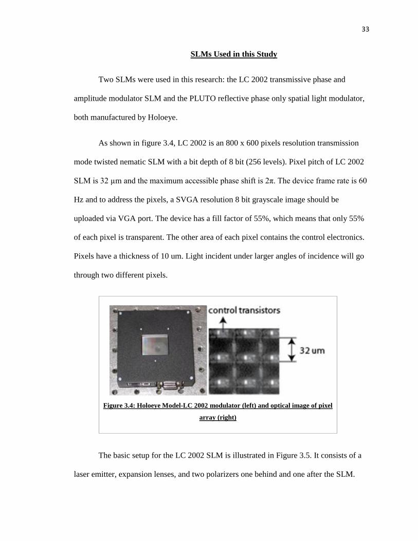
As shown in figure 3.4, LC 2002 is an 800 x 600 pixels resolution transmission
mode twisted nematic SLM with a bit depth of 8 bit (256 levels). Pixel pitch of LC 2002
SLM is 32 µm and the maximum accessible phase shift is 2π. The device frame rate is 60
Hz and to address the pixels, a SVGA resolution 8 bit grayscale image should be
uploaded via VGA port. The device has a fill factor of 55%, which means that only 55%
of each pixel is transparent. The other area of each pixel contains the control electronics.
Pixels have a thickness of 10 um. Light incident under larger angles of incidence will go
through two different pixels.
The basic setup for the LC 2002 SLM is illustrated in Figure 3.5. It consists of a
laser emitter, expansion lenses, and two polarizers one behind and one after the SLM.
Figure 3.4: Holoeye Model-LC 2002 modulator (left) and optical image of pixel
array (right)
34
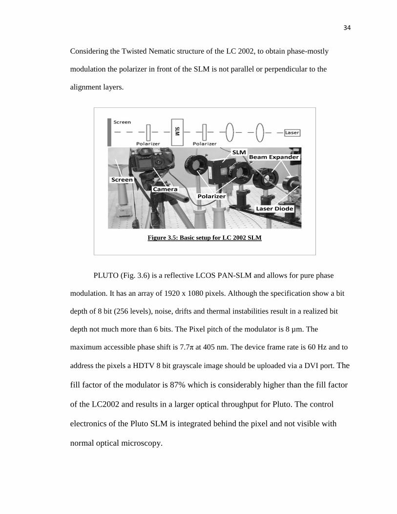
Considering the Twisted Nematic structure of the LC 2002, to obtain phase-mostly
modulation the polarizer in front of the SLM is not parallel or perpendicular to the
alignment layers.
PLUTO (Fig. 3.6) is a reflective LCOS PAN-SLM and allows for pure phase
modulation. It has an array of 1920 x 1080 pixels. Although the specification show a bit
depth of 8 bit (256 levels), noise, drifts and thermal instabilities result in a realized bit
depth not much more than 6 bits. The Pixel pitch of the modulator is 8 µm. The
maximum accessible phase shift is 7.7π at 405 nm. The device frame rate is 60 Hz and to
address the pixels a HDTV 8 bit grayscale image should be uploaded via a DVI port. The
fill factor of the modulator is 87% which is considerably higher than the fill factor
of the LC2002 and results in a larger optical throughput for Pluto. The control
electronics of the Pluto SLM is integrated behind the pixel and not visible with
normal optical microscopy.
Figure 3.5: Basic setup for LC 2002 SLM
35
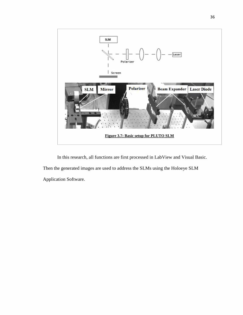
The basic setup for the PLUTO SLM is illustrated in Figure 3.7 which consists of
laser emitter, expansion lenses, a polarizer in front and behind the SLM, and a semi-
transparent mirror (i.e. a beamsplitter). Note that in Figure 3.7 the modulator is
positioned behind the beam splitter cube, and that the 2nd polarizer and projection screen
are not included in the figure.
Figure 3.6: Holoeye PLUTO modulator (left) and optical image of pixel array (right).
36
In this research, all functions are first processed in LabView and Visual Basic.
Then the generated images are used to address the SLMs using the Holoeye SLM
Application Software.
Figure 3.7: Basic setup for PLUTO SLM
37
CHAPTER IV: MULTI LENS TECHNIQUE FOR BEAM SHAPING
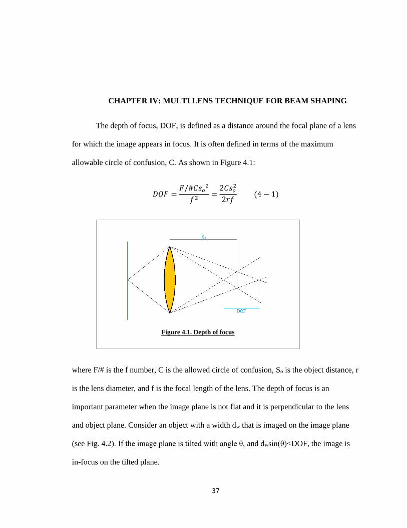
The depth of focus, DOF, is defined as a distance around the focal plane of a lens
for which the image appears in focus. It is often defined in terms of the maximum
allowable circle of confusion, C. As shown in Figure 4.1:
𝐷𝑂𝐹 =𝐹/#𝐶𝑠𝑜
2
𝑓2=2𝐶𝑠𝑜
2
2𝑟𝑓 (4 − 1)
where F/# is the f number, C is the allowed circle of confusion, So is the object distance, r
is the lens diameter, and f is the focal length of the lens. The depth of focus is an
important parameter when the image plane is not flat and it is perpendicular to the lens
and object plane. Consider an object with a width dw that is imaged on the image plane
(see Fig. 4.2). If the image plane is tilted with angle θ, and dwsin(θ)<DOF, the image is
in-focus on the tilted plane.
Figure 4.1. Depth of focus
38
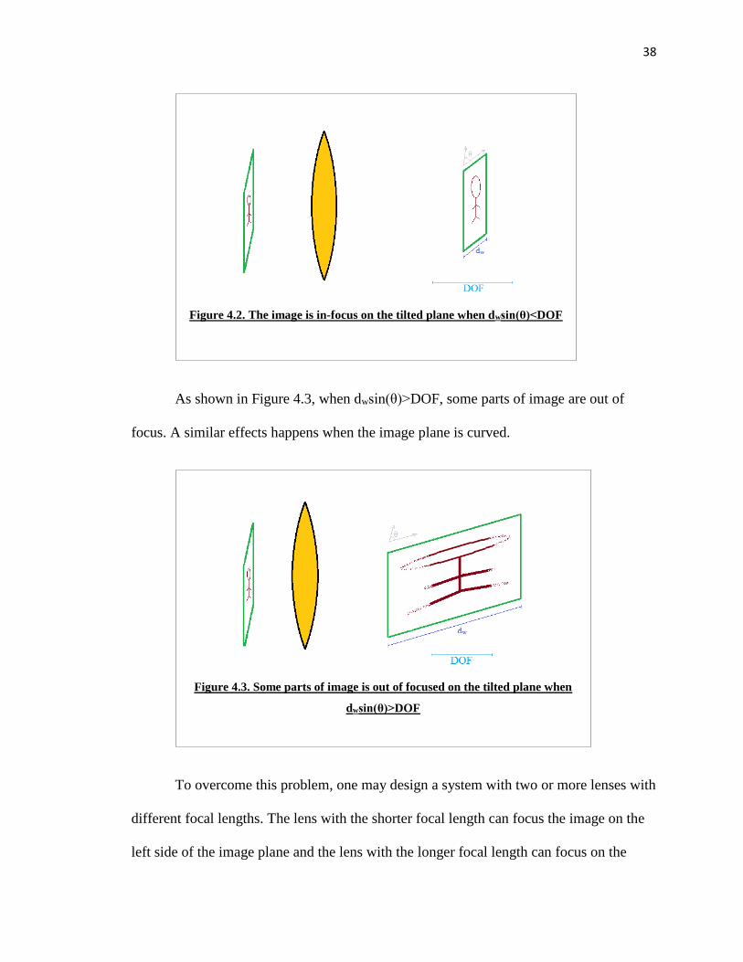
As shown in Figure 4.3, when dwsin(θ)>DOF, some parts of image are out of
focus. A similar effects happens when the image plane is curved.
To overcome this problem, one may design a system with two or more lenses with
different focal lengths. The lens with the shorter focal length can focus the image on the
left side of the image plane and the lens with the longer focal length can focus on the
Figure 4.3. Some parts of image is out of focused on the tilted plane when
dwsin(θ)>DOF
Figure 4.2. The image is in-focus on the tilted plane when dwsin(θ)<DOF
39
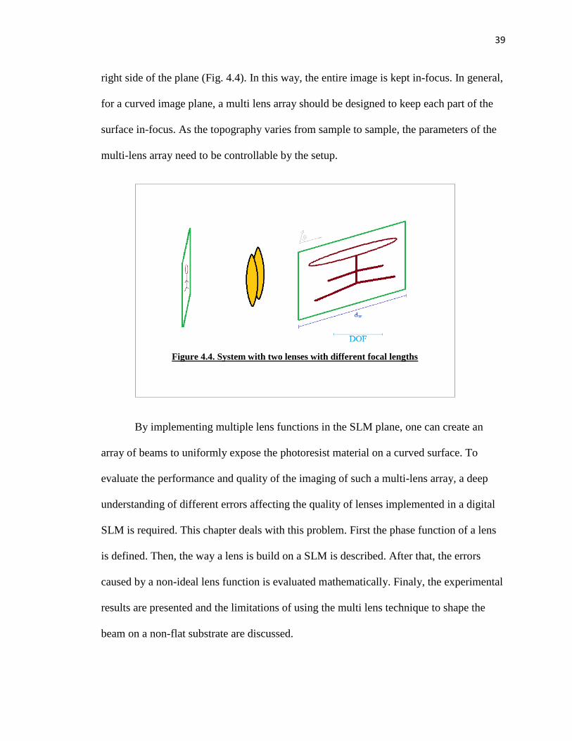
right side of the plane (Fig. 4.4). In this way, the entire image is kept in-focus. In general,
for a curved image plane, a multi lens array should be designed to keep each part of the
surface in-focus. As the topography varies from sample to sample, the parameters of the
multi-lens array need to be controllable by the setup.
By implementing multiple lens functions in the SLM plane, one can create an
array of beams to uniformly expose the photoresist material on a curved surface. To
evaluate the performance and quality of the imaging of such a multi-lens array, a deep
understanding of different errors affecting the quality of lenses implemented in a digital
SLM is required. This chapter deals with this problem. First the phase function of a lens
is defined. Then, the way a lens is build on a SLM is described. After that, the errors
caused by a non-ideal lens function is evaluated mathematically. Finaly, the experimental
results are presented and the limitations of using the multi lens technique to shape the
beam on a non-flat substrate are discussed.
Figure 4.4. System with two lenses with different focal lengths

40
The Phase Function of a Lens Implemented on a LC SLM
An SLM can be used to create an optical refracting device such as a prism or a
lens. To realize a converging lens in a SLM, the phase pattern image loaded in the SLM
should be proportional to the thickness function of the lens [30]. A biconvex lens has a
thickness distribution ∆(x,y) that is given by:
2
2
22
22
1
22
1 1111,R
yxR
R
yxRyx o
(4-2)
where Δo is the lens thickness at the center between the two lens vertices, and R1 and R2
are the radii of surface curvature of the first and 2nd refracting surface. x and y are the
distances from the optical axis in the x- and y-directions. The optical axis is the line that
is perpendicular to the lens going through its center. For paraxial rays, the square roots in
equation (4-2) can be replaced by their Taylor approximation, i.e. √1 − 𝑥 = 1 −𝑥
2
resulting in [31]:
21
22 11
2,
RR
yxyx o
(4-3)
Assuming the lens refraction index is n0 and assuming it is placed in air, the phase shift
caused by the lens on a ray passing through lens position (x,y) is given by (in radians):
21
22 111
21
2,
RRn
yxnyx o
(4-4)
Using the lensmaker’s equation this can be written in terms of the focal distance f:

41
22
2
11
2, yx
fnyx o
(4-5)
Which describes the phase function of a lens with focal distance f. Note that a lens
described by equation (4-5) is no longer a spherical lens and has no spherical aberration
for a point on the optical axis.
Instead of varying the thickness as a function of x and y, a lens can also be
implemented by varying the refraction index and keeping the thickness constant. This
kind of lenses are called Gradient Index (GRIN) Lenses. The refractive index profile of a
GRIN Lens has the following form [32]
(4-6)
where α, 2, 3, are constants that define the focal length of the lens. Neglecting higher
order terms and using the approximation of √1 + 𝑥 = 1 + 𝑥
2
2225.01 yxann o (4-7)
The phase function realized by such GRIN lens is given by:
2225.0
2, yxdnadnyx oo
(4-8)
Note that both equation (4-5) and (4-8) have the same position dependence. Furthermore
note that the GRIN lens of equation (4-7) has also no spherical aberration. [33].
It is possible to implement such lenses in a phase LC-SLM since the refraction
index of any pixel can be electronically controlled. Note that these lenses do not have
𝑛2 = 𝑛02[1 − (𝛼𝑟)2 + 𝛼2(𝛼𝑟)
4 + 𝛼3(𝛼𝑟)6 +⋯ ]
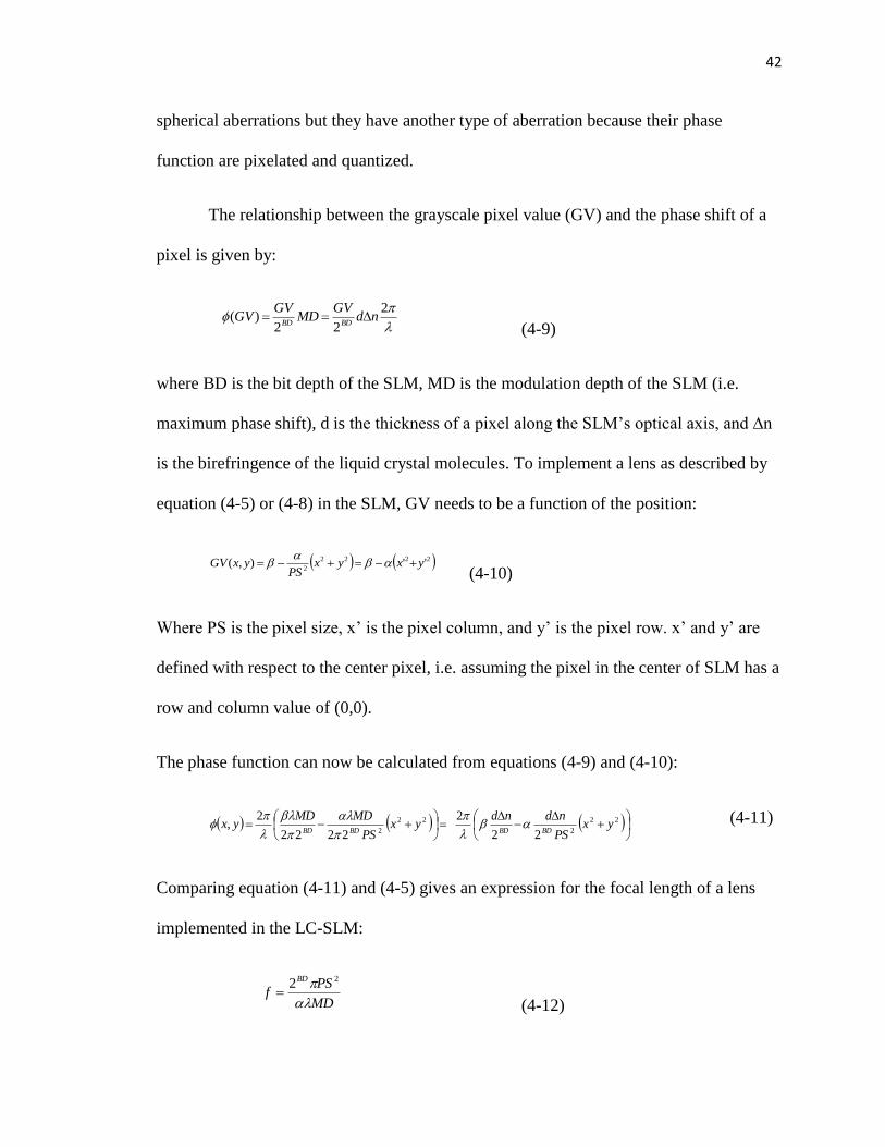
42
spherical aberrations but they have another type of aberration because their phase
function are pixelated and quantized.
The relationship between the grayscale pixel value (GV) and the phase shift of a
pixel is given by:
2
22)( nd
GVMD
GVGV
BDBD
(4-9)
where BD is the bit depth of the SLM, MD is the modulation depth of the SLM (i.e.
maximum phase shift), d is the thickness of a pixel along the SLM’s optical axis, and ∆n
is the birefringence of the liquid crystal molecules. To implement a lens as described by
equation (4-5) or (4-8) in the SLM, GV needs to be a function of the position:
2222
2''),( yxyx
PSyxGV
(4-10)
Where PS is the pixel size, x’ is the pixel column, and y’ is the pixel row. x’ and y’ are
defined with respect to the center pixel, i.e. assuming the pixel in the center of SLM has a
row and column value of (0,0).
The phase function can now be calculated from equations (4-9) and (4-10):
22
2
22
2 22
2
2222
2, yx
PS
ndndyx
PS
MDMDyx
BDBDBDBD
(4-11)
Comparing equation (4-11) and (4-5) gives an expression for the focal length of a lens
implemented in the LC-SLM:
MD
PSf
BD
22
(4-12)
43
A program was written in Visual Basic to calculate the gray scale image for a particular
lens function. The input parameters of the program were α and β. The image pattern is
then transferred to the LCD via a VGA port and a program written was in Labview 2011.
In the rest of the chapter the lens function is investigated theoretically and
experimentally.
Lenses Implemented in an SLM
In this study, the LC-2002 LC-SLM which has 800×600 pixels is used. The
refraction index of each pixel can be controlled by loading the pixel with a gray-scale
value between zero and 255. So, the pixel depth, BD, is 8 bits. The maximum diameter of
a circular lens that can be implemented in the LC-2002 LC-SLM is 600 pixels or 19.2
mm. Although GV can be defined for all pixels of the SLM, i.e. -400<x’≤400 and -
300<y’≤300, in the followings, only the pixels that have a distance 300'' 22 yx from
the center pixel of the SLM will be considered. So, the focus is on the performance of a
lens with a circular entrance pupil.
Any value of GV(x’, y’) in the generated image is considered as an 8bit grayscale
color. The grayscale image, after transferring to the LC-SLM, is translated into the
corresponding phase function. The phase shift that the LC-SLM generates for minimum
and maximum color values depends on its internal structure and can be calculated from
equation (4-9). The focal length of the realized lens depends on α, and it can be
calculated from equation (4-12).

44
To have a lens function which covers the whole area of the LC-SLM and that uses
the full range of the BD, one should consider β=255 and 𝛼 =255
3002= 0.00283 which
makes the maximum grayscale value at the center of the LC-SLM and the minimum
grayscale value near the edge of the lens. The generated image is shown in Figure 4.5.
The pixel values outside the lens’ entrance pupil are kept at zero. The corresponding
focal length for the LC2002 at 532 nm following from equation (4-12) is very large and
equal to 87.06 meters.
To have a better understanding of the phase distribution in the designed lens
surface, the grayscale value along the x axis (y=0) of the LC-SLM is plotted in figure 4.6.
Figure 4.5: Phase Image of the lens function with n0=255 and α= 0.00283
(f=87.06m for LC-SLM at 532nm).
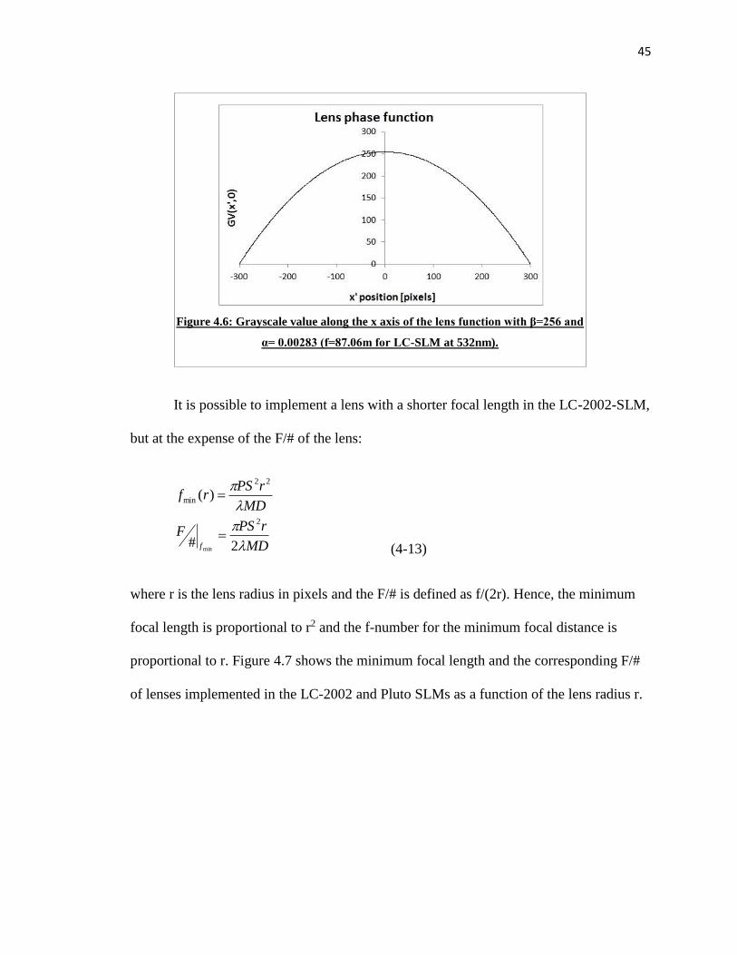
45
It is possible to implement a lens with a shorter focal length in the LC-2002-SLM,
but at the expense of the F/# of the lens:
MD
rPSF
MD
rPSrf
f
2#
)(
2
22
min
min
(4-13)
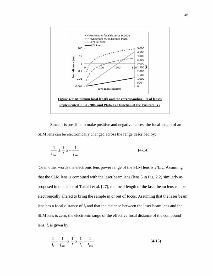
where r is the lens radius in pixels and the F/# is defined as f/(2r). Hence, the minimum
focal length is proportional to r2 and the f-number for the minimum focal distance is
proportional to r. Figure 4.7 shows the minimum focal length and the corresponding F/#
of lenses implemented in the LC-2002 and Pluto SLMs as a function of the lens radius r.
Figure 4.6: Grayscale value along the x axis of the lens function with β=256 and
α= 0.00283 (f=87.06m for LC-SLM at 532nm).
46
Since it is possible to make positive and negative lenses, the focal length of an
SLM lens can be electronically changed across the range described by:
minmin
11
f
1
ff (4-14)
Or in other words the electronic lens power range of the SLM lens is 2/fmin. Assuming
that the SLM lens is combined with the laser beam lens (lens 3 in Fig. 2.2) similarly as
proposed in the paper of Takaki et al. [27], the focal length of the laser beam lens can be
electronically altered to bring the sample in or out of focus. Assuming that the laser beam
lens has a focal distance of fr and that the distance between the laser beam lens and the
SLM lens is zero, the electronic range of the effective focal distance of the compound
lens, f, is given by:
minmin
11111
fffff rr
(4-15)
Figure 4.7: Minimum focal length and the corresponding F/# of lenses
implemented in LC-2002 and Pluto as a function of the lens radius r
47
Lens 3 and the objective form an image of the beam aperture on the sample. Of course
the image distance is a function of the focal length of the compound lens and can be
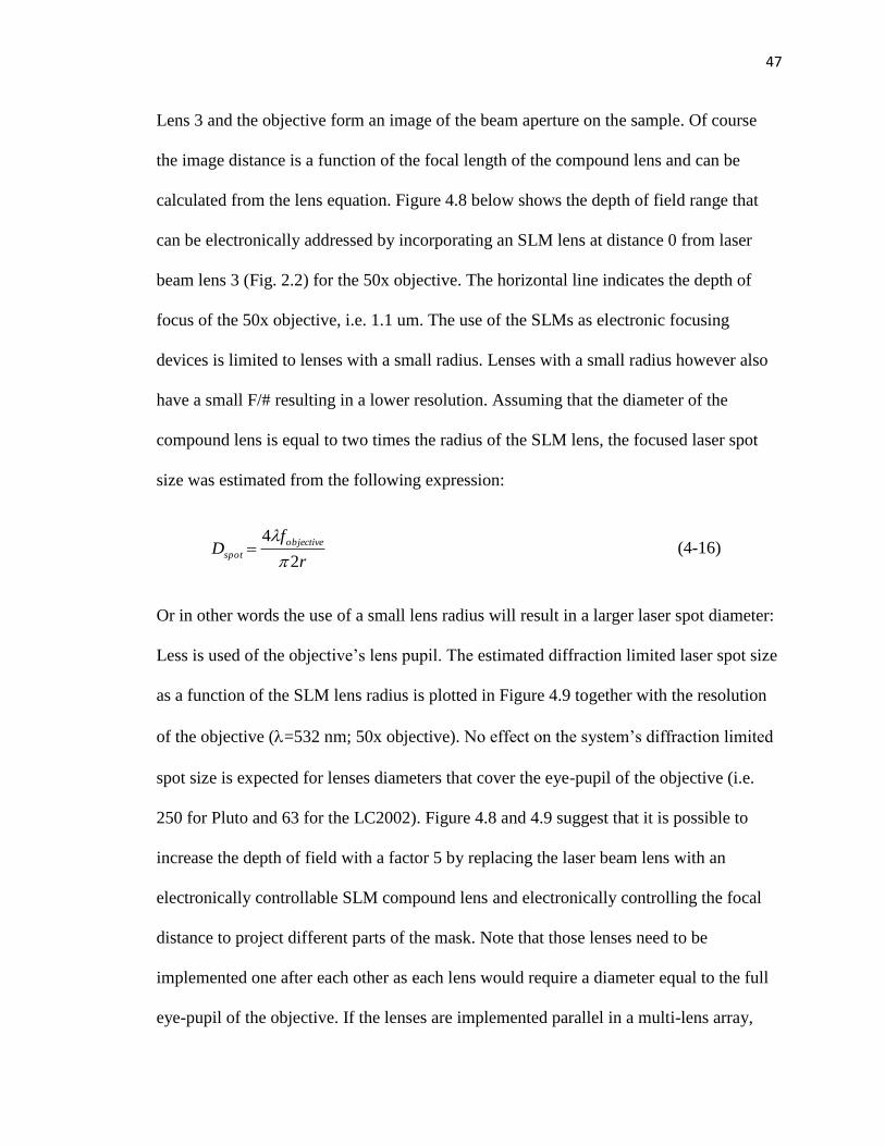
calculated from the lens equation. Figure 4.8 below shows the depth of field range that
can be electronically addressed by incorporating an SLM lens at distance 0 from laser
beam lens 3 (Fig. 2.2) for the 50x objective. The horizontal line indicates the depth of
focus of the 50x objective, i.e. 1.1 um. The use of the SLMs as electronic focusing
devices is limited to lenses with a small radius. Lenses with a small radius however also
have a small F/# resulting in a lower resolution. Assuming that the diameter of the
compound lens is equal to two times the radius of the SLM lens, the focused laser spot
size was estimated from the following expression:
r
fD
objective
spot2
4
(4-16)
Or in other words the use of a small lens radius will result in a larger laser spot diameter:
Less is used of the objective’s lens pupil. The estimated diffraction limited laser spot size
as a function of the SLM lens radius is plotted in Figure 4.9 together with the resolution
of the objective (=532 nm; 50x objective). No effect on the system’s diffraction limited
spot size is expected for lenses diameters that cover the eye-pupil of the objective (i.e.
250 for Pluto and 63 for the LC2002). Figure 4.8 and 4.9 suggest that it is possible to
increase the depth of field with a factor 5 by replacing the laser beam lens with an
electronically controllable SLM compound lens and electronically controlling the focal
distance to project different parts of the mask. Note that those lenses need to be
implemented one after each other as each lens would require a diameter equal to the full
eye-pupil of the objective. If the lenses are implemented parallel in a multi-lens array,
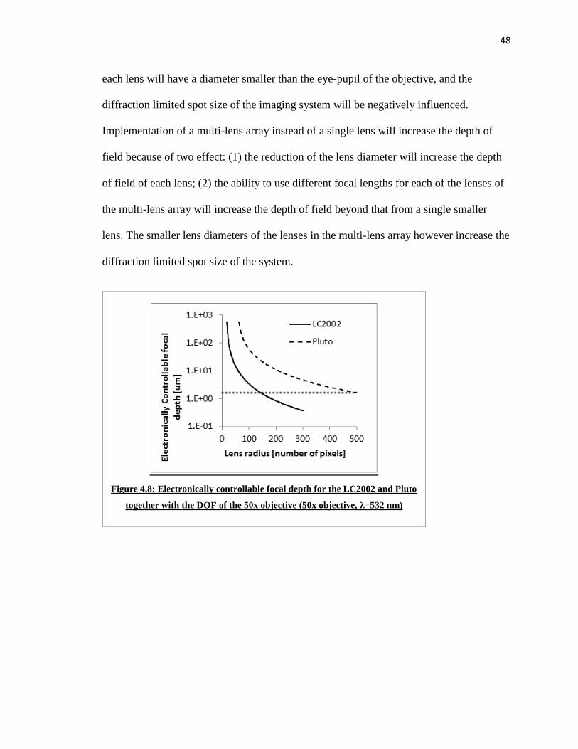
48
each lens will have a diameter smaller than the eye-pupil of the objective, and the
diffraction limited spot size of the imaging system will be negatively influenced.
Implementation of a multi-lens array instead of a single lens will increase the depth of
field because of two effect: (1) the reduction of the lens diameter will increase the depth
of field of each lens; (2) the ability to use different focal lengths for each of the lenses of
the multi-lens array will increase the depth of field beyond that from a single smaller
lens. The smaller lens diameters of the lenses in the multi-lens array however increase the
diffraction limited spot size of the system.
Figure 4.8: Electronically controllable focal depth for the LC2002 and Pluto
together with the DOF of the 50x objective (50x objective, λ=532 nm)
49
Expansion of the electronically controllable DOF to a larger range requires SLM
lenses with a larger focal distance. To implement stronger lenses, one can use a Fresnel
lens approach: The light cannot see the difference between a 2π, 4π, or 6π phase shift, so
it is possible to use the modulus function. Hence phase shifts ϕ that are larger than 2π can
be implemented by loading the pixel with the gray scale value mod (ϕ,2π). This approach
allows us to implement a GV function with an α value beyond 2𝐵𝐷−1
𝑟2.
The modulus function was implemented as follows:
𝐺𝑉(𝑥′, 𝑦′) =
{
𝛽−𝛼(𝑥′2+𝑦′2) 0≤𝛽−𝛼(𝑥′2+𝑦′2)<256
𝛽−𝛼(𝑥′2+𝑦′2)+256 −256≤𝛽−𝛼(𝑥′2+𝑦′2)<0
𝛽−𝛼(𝑥′2+𝑦′
2)+512 −512≤𝛽−𝛼(𝑥′
2+𝑦′
2)<−256
.
.
.
𝛽−𝛼(𝑥′2+𝑦′2)+256𝑘 −256𝑘≤𝛽−𝛼(𝑥′2+𝑦′2)<−256(𝑘−1)
(Eq. 4-17)
Solving the boundaries for r≥0 gives:
Figure 4.9: Diffraction limited spot size of focused laser beam together with
system resolution without electronic focusing (50x objective, λ =532 nm)
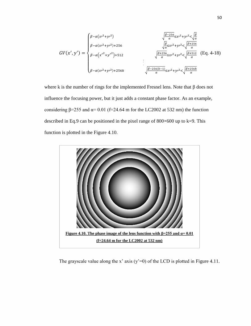
50
𝐺𝑉(𝑥′, 𝑦′) =
{
𝛽−𝛼(𝑥′
2+𝑦′2) √𝛽−256
𝛼≤𝑥′2+𝑦′2<√
𝛽
𝛼
𝛽−𝛼(𝑥′2+𝑦′2)+256 √𝛽
𝛼≤𝑥′2+𝑦′2<√
𝛽+256
𝛼
𝛽−𝛼(𝑥′2+𝑦′
2)+512 √
𝛽+256
𝛼≤𝑥′2+𝑦′2<√
𝛽+512
𝛼...
𝛽−𝛼(𝑥′2+𝑦′2)+256𝑘 √𝛽−256(𝑘−1)
𝛼≤𝑥′2+𝑦′2<√
𝛽+256𝑘
𝛼
(Eq. 4-18)
where k is the number of rings for the implemented Fresnel lens. Note that β does not
influence the focusing power, but it just adds a constant phase factor. As an example,
considering β=255 and α= 0.01 (f=24.64 m for the LC2002 at 532 nm) the function
described in Eq.9 can be positioned in the pixel range of 800×600 up to k=9. This
function is plotted in the Figure 4.10.
The grayscale value along the x’ axis (y’=0) of the LCD is plotted in Figure 4.11.
Figure 4.10. The phase image of the lens function with β=255 and α= 0.01
(f=24.64 m for the LC2002 at 532 nm)
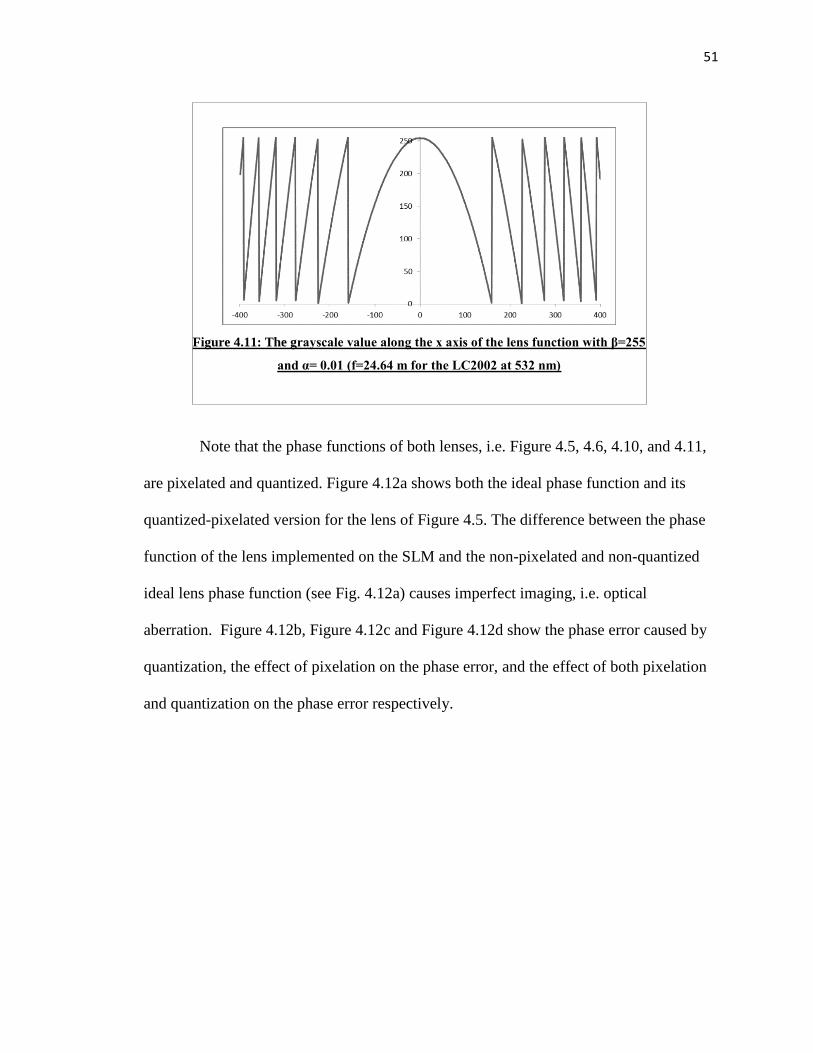
51
Note that the phase functions of both lenses, i.e. Figure 4.5, 4.6, 4.10, and 4.11,
are pixelated and quantized. Figure 4.12a shows both the ideal phase function and its
quantized-pixelated version for the lens of Figure 4.5. The difference between the phase
function of the lens implemented on the SLM and the non-pixelated and non-quantized
ideal lens phase function (see Fig. 4.12a) causes imperfect imaging, i.e. optical
aberration. Figure 4.12b, Figure 4.12c and Figure 4.12d show the phase error caused by
quantization, the effect of pixelation on the phase error, and the effect of both pixelation
and quantization on the phase error respectively.
Figure 4.11: The grayscale value along the x axis of the lens function with β=255
and α= 0.01 (f=24.64 m for the LC2002 at 532 nm)
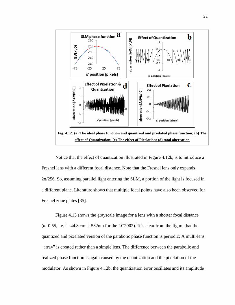
52
Notice that the effect of quantization illustrated in Figure 4.12b, is to introduce a
Fresnel lens with a different focal distance. Note that the Fresnel lens only expands
2/256. So, assuming parallel light entering the SLM, a portion of the light is focused in
a different plane. Literature shows that multiple focal points have also been observed for
Fresnel zone plates [35].
Figure 4.13 shows the grayscale image for a lens with a shorter focal distance
(α=0.55, i.e. f= 44.8 cm at 532nm for the LC2002). It is clear from the figure that the
quantized and pixelated version of the parabolic phase function is periodic; A multi-lens
“array” is created rather than a simple lens. The difference between the parabolic and
realized phase function is again caused by the quantization and the pixelation of the
modulator. As shown in Figure 4.12b, the quantization error oscillates and its amplitude
Fig. 4.12: (a) The ideal phase function and quantized and pixelated phase function; (b) The
effect of Quantization; (c) The effect of Pixelation; (d) total aberration
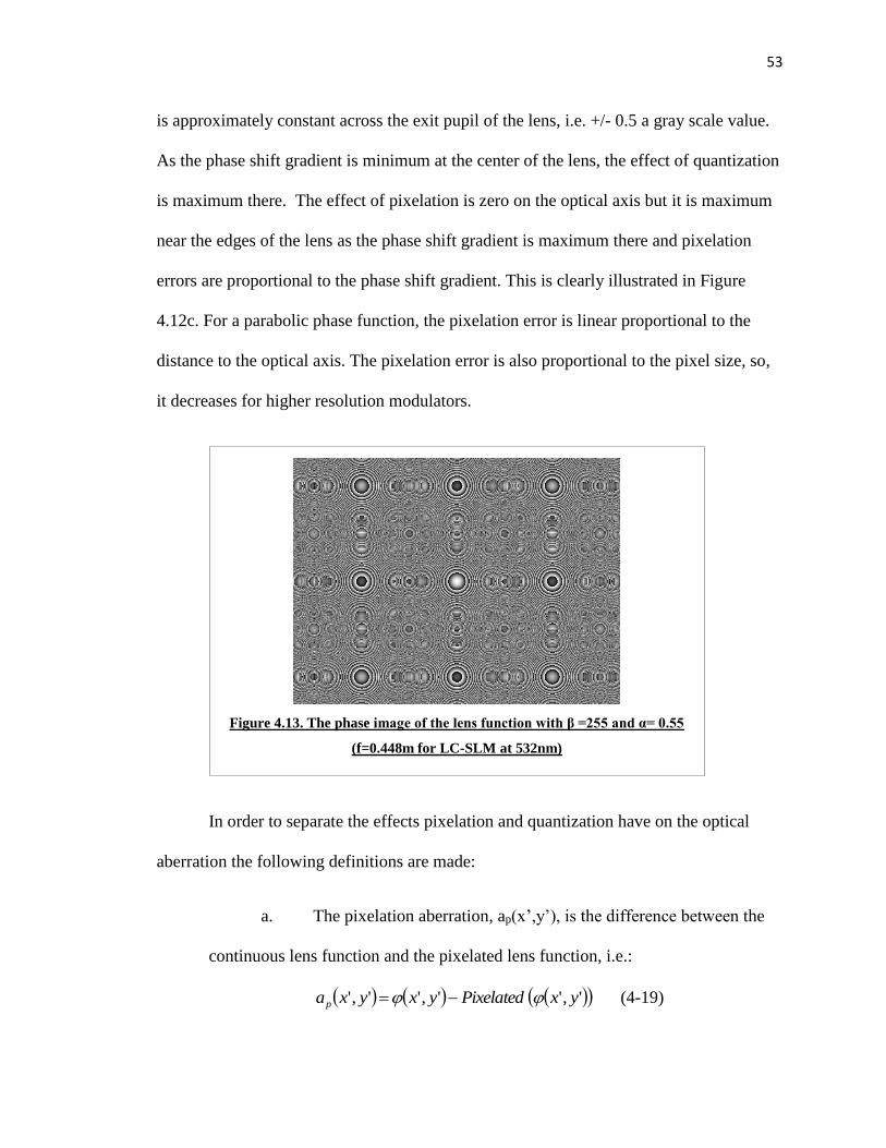
53
is approximately constant across the exit pupil of the lens, i.e. +/- 0.5 a gray scale value.
As the phase shift gradient is minimum at the center of the lens, the effect of quantization
is maximum there. The effect of pixelation is zero on the optical axis but it is maximum
near the edges of the lens as the phase shift gradient is maximum there and pixelation
errors are proportional to the phase shift gradient. This is clearly illustrated in Figure
4.12c. For a parabolic phase function, the pixelation error is linear proportional to the
distance to the optical axis. The pixelation error is also proportional to the pixel size, so,
it decreases for higher resolution modulators.
In order to separate the effects pixelation and quantization have on the optical
aberration the following definitions are made:
a. The pixelation aberration, ap(x’,y’), is the difference between the
continuous lens function and the pixelated lens function, i.e.:
','','',' yxPixelatedyxyxap (4-19)
Figure 4.13. The phase image of the lens function with β =255 and α= 0.55
(f=0.448m for LC-SLM at 532nm)
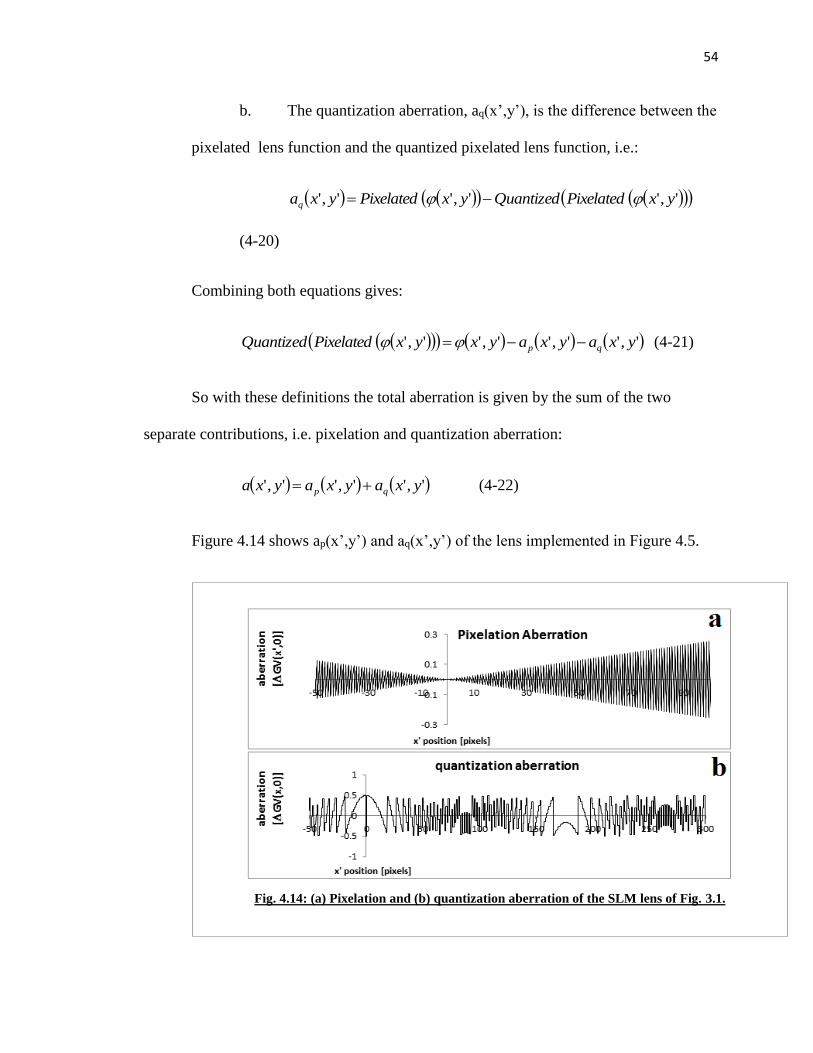
54
b. The quantization aberration, aq(x’,y’), is the difference between the
pixelated lens function and the quantized pixelated lens function, i.e.:
','','',' yxPixelatedQuantizedyxPixelatedyxaq
(4-20)
Combining both equations gives:
','','','',' yxayxayxyxPixelatedQuantized qp (4-21)
So with these definitions the total aberration is given by the sum of the two
separate contributions, i.e. pixelation and quantization aberration:
','','',' yxayxayxa qp (4-22)
Figure 4.14 shows ap(x’,y’) and aq(x’,y’) of the lens implemented in Figure 4.5.
Fig. 4.14: (a) Pixelation and (b) quantization aberration of the SLM lens of Fig. 3.1.
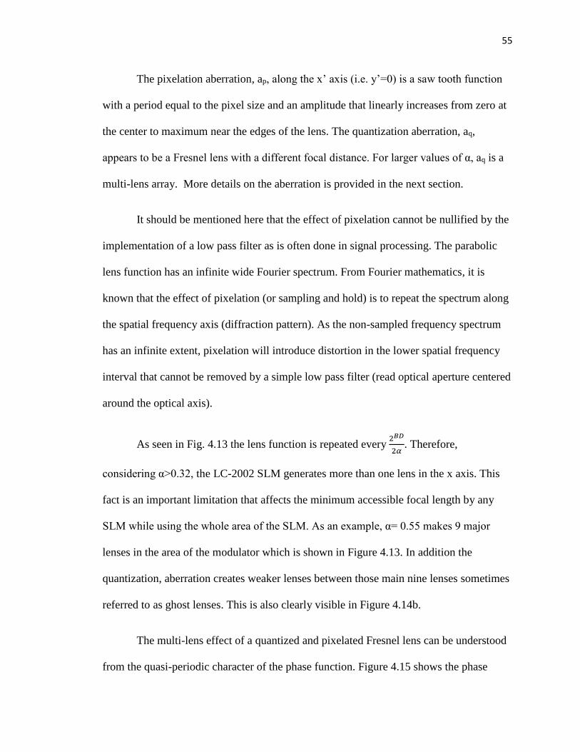
55
The pixelation aberration, ap, along the x’ axis (i.e. y’=0) is a saw tooth function
with a period equal to the pixel size and an amplitude that linearly increases from zero at
the center to maximum near the edges of the lens. The quantization aberration, aq,
appears to be a Fresnel lens with a different focal distance. For larger values of α, aq is a
multi-lens array. More details on the aberration is provided in the next section.
It should be mentioned here that the effect of pixelation cannot be nullified by the
implementation of a low pass filter as is often done in signal processing. The parabolic
lens function has an infinite wide Fourier spectrum. From Fourier mathematics, it is
known that the effect of pixelation (or sampling and hold) is to repeat the spectrum along
the spatial frequency axis (diffraction pattern). As the non-sampled frequency spectrum
has an infinite extent, pixelation will introduce distortion in the lower spatial frequency
interval that cannot be removed by a simple low pass filter (read optical aperture centered
around the optical axis).
As seen in Fig. 4.13 the lens function is repeated every 2𝐵𝐷
2𝛼. Therefore,
considering α>0.32, the LC-2002 SLM generates more than one lens in the x axis. This
fact is an important limitation that affects the minimum accessible focal length by any
SLM while using the whole area of the SLM. As an example, α= 0.55 makes 9 major
lenses in the area of the modulator which is shown in Figure 4.13. In addition the
quantization, aberration creates weaker lenses between those main nine lenses sometimes
referred to as ghost lenses. This is also clearly visible in Figure 4.14b.
The multi-lens effect of a quantized and pixelated Fresnel lens can be understood
from the quasi-periodic character of the phase function. Figure 4.15 shows the phase
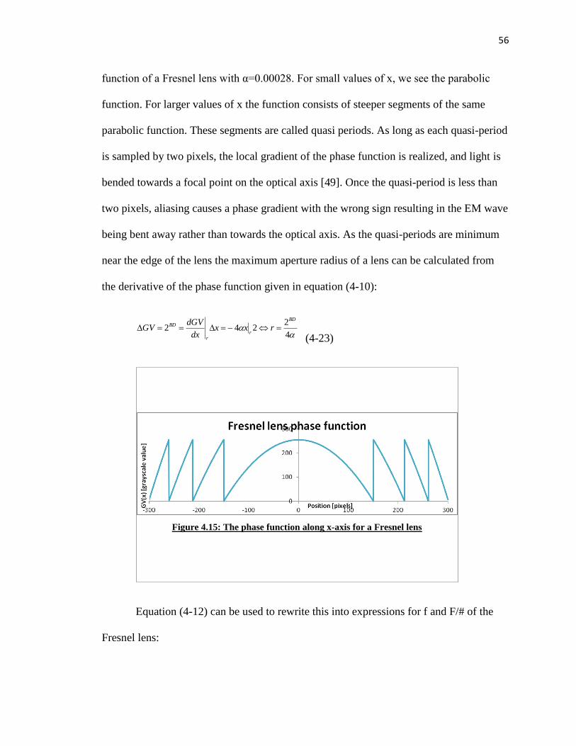
56
function of a Fresnel lens with α=0.00028. For small values of x, we see the parabolic
function. For larger values of x the function consists of steeper segments of the same
parabolic function. These segments are called quasi periods. As long as each quasi-period
is sampled by two pixels, the local gradient of the phase function is realized, and light is
bended towards a focal point on the optical axis [49]. Once the quasi-period is less than
two pixels, aliasing causes a phase gradient with the wrong sign resulting in the EM wave
being bent away rather than towards the optical axis. As the quasi-periods are minimum
near the edge of the lens the maximum aperture radius of a lens can be calculated from
the derivative of the phase function given in equation (4-10):
4
2242
BD
rr
BD rxxdx
dGVGV
(4-23)
Equation (4-12) can be used to rewrite this into expressions for f and F/# of the
Fresnel lens:
Figure 4.15: The phase function along x-axis for a Fresnel lens
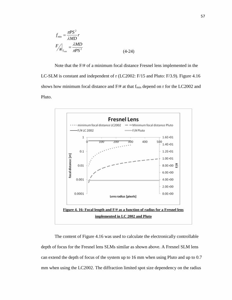
57
2
2
min
min# PS
MDF
rMD
PSf
f
(4-24)
Note that the F/# of a minimum focal distance Fresnel lens implemented in the
LC-SLM is constant and independent of r (LC2002: F/15 and Pluto: F/3.9). Figure 4.16
shows how minimum focal distance and F/# at that fmin depend on r for the LC2002 and
Pluto.
The content of Figure 4.16 was used to calculate the electronically controllable
depth of focus for the Fresnel lens SLMs similar as shown above. A Fresnel SLM lens
can extend the depth of focus of the system up to 16 mm when using Pluto and up to 0.7
mm when using the LC2002. The diffraction limited spot size dependency on the radius
Figure 4. 16: Focal length and F/# as a function of radius for a Fresnel lens
implemented in LC 2002 and Pluto

58
of the lens is similar as for the non-Fresnel SLM lens. No impact on the diffraction
limited spot size is expected for lens radii of 2 mm and above. This corresponds to the
radius of the objective’s eye-pupil (larger than 63 pixels for the LC2002 and larger than
250 pixels for Pluto).
Statistical Analysis on Pixelation and Quantization Aberration
As an example, for a lens with β=255 and α= 0.01, the calculated GV(x’,y’) value
is an integer number in 12480 pixels of the LCD. It means that for this lens, the
calculated GV(x’,y’) value is exactly equal to the specified grayscale value only in 2.6%
of the pixels (P = 2.6%). Other 97.4% of the pixels are rounded to the nearest integer
number. Figure 3.17 shows the difference between the pixels of this lens and the nearest
integer. As illustrated in this figure, 52.6% of pixels are 0.25 off from the nearest integer
number.
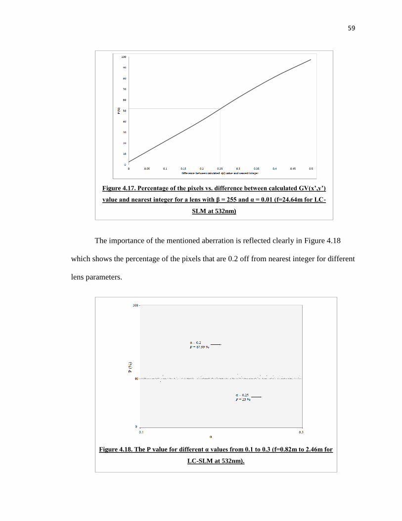
59
The importance of the mentioned aberration is reflected clearly in Figure 4.18
which shows the percentage of the pixels that are 0.2 off from nearest integer for different
lens parameters.
Figure 4.18. The P value for different α values from 0.1 to 0.3 (f=0.82m to 2.46m for
LC-SLM at 532nm).
Figure 4.17. Percentage of the pixels vs. difference between calculated GV(x’,y’)
value and nearest integer for a lens with β = 255 and α = 0.01 (f=24.64m for LC-
SLM at 532nm)
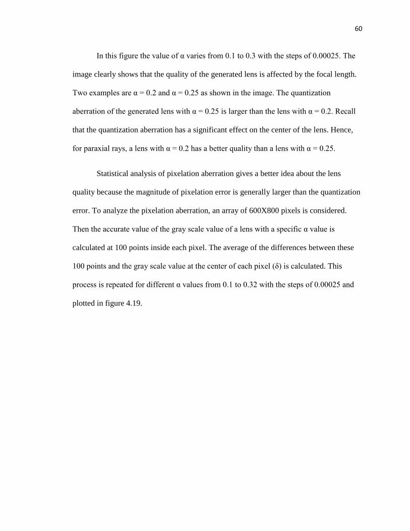
60
In this figure the value of α varies from 0.1 to 0.3 with the steps of 0.00025. The
image clearly shows that the quality of the generated lens is affected by the focal length.
Two examples are α = 0.2 and α = 0.25 as shown in the image. The quantization
aberration of the generated lens with α = 0.25 is larger than the lens with α = 0.2. Recall
that the quantization aberration has a significant effect on the center of the lens. Hence,
for paraxial rays, a lens with α = 0.2 has a better quality than a lens with α = 0.25.
Statistical analysis of pixelation aberration gives a better idea about the lens
quality because the magnitude of pixelation error is generally larger than the quantization
error. To analyze the pixelation aberration, an array of 600X800 pixels is considered.
Then the accurate value of the gray scale value of a lens with a specific α value is
calculated at 100 points inside each pixel. The average of the differences between these
100 points and the gray scale value at the center of each pixel (δ) is calculated. This
process is repeated for different α values from 0.1 to 0.32 with the steps of 0.00025 and
plotted in figure 4.19.
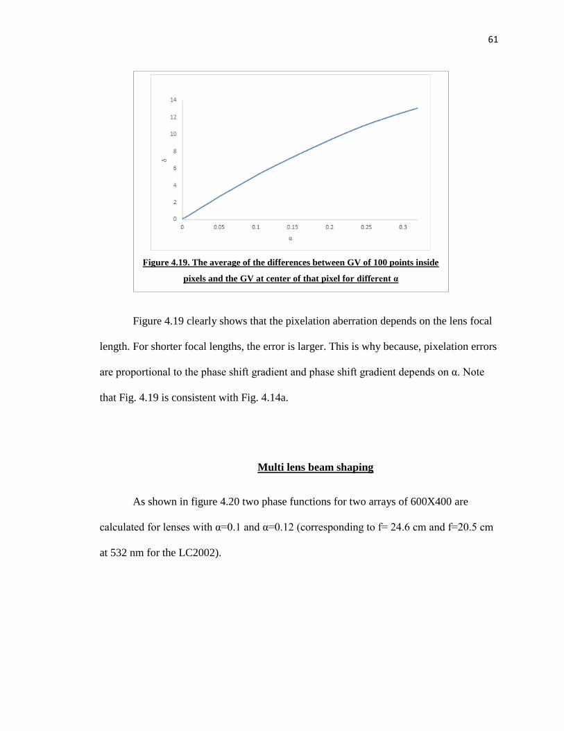
61
Figure 4.19 clearly shows that the pixelation aberration depends on the lens focal
length. For shorter focal lengths, the error is larger. This is why because, pixelation errors
are proportional to the phase shift gradient and phase shift gradient depends on α. Note
that Fig. 4.19 is consistent with Fig. 4.14a.
Multi lens beam shaping
As shown in figure 4.20 two phase functions for two arrays of 600X400 are
calculated for lenses with α=0.1 and α=0.12 (corresponding to f= 24.6 cm and f=20.5 cm
at 532 nm for the LC2002).
Figure 4.19. The average of the differences between GV of 100 points inside
pixels and the GV at center of that pixel for different α
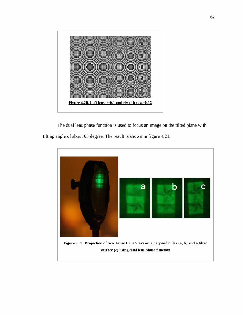
62
The dual lens phase function is used to focus an image on the tilted plane with
tilting angle of about 65 degree. The result is shown in figure 4.21.
Figure 4.21. Projection of two Texas Lone Stars on a perpendicular (a, b) and a tilted
surface (c) using dual lens phase function
Figure 4.20. Left lens α=0.1 and right lens α=0.12
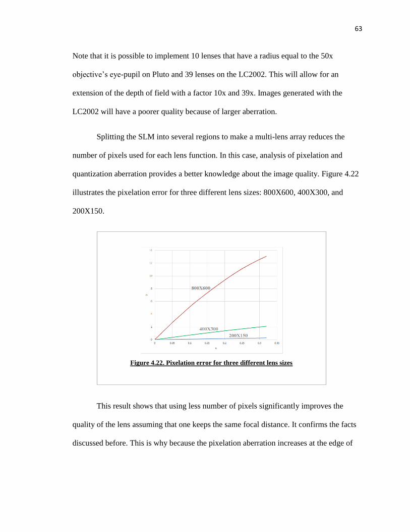
63
Note that it is possible to implement 10 lenses that have a radius equal to the 50x
objective’s eye-pupil on Pluto and 39 lenses on the LC2002. This will allow for an
extension of the depth of field with a factor 10x and 39x. Images generated with the
LC2002 will have a poorer quality because of larger aberration.
Splitting the SLM into several regions to make a multi-lens array reduces the
number of pixels used for each lens function. In this case, analysis of pixelation and
quantization aberration provides a better knowledge about the image quality. Figure 4.22
illustrates the pixelation error for three different lens sizes: 800X600, 400X300, and
200X150.
This result shows that using less number of pixels significantly improves the
quality of the lens assuming that one keeps the same focal distance. It confirms the facts
discussed before. This is why because the pixelation aberration increases at the edge of
Figure 4.22. Pixelation error for three different lens sizes
64
the lens: reducing the number of pixels cut the edges and reduces the pixelation
aberration.
However, by having a very small size lens the quantization aberration becomes
more important. For a very small size lens, pixelation aberration is close to zero and
neglectable. But, the quantization aberration which has a magnitude from 0 to 0.5 affects
the quality because the gray scale value is also very small near the center of the lens.
In addition to aberration a smaller size lens increases the depth of field as the
numerical aperture of the system decreases (see equation 4-1). A smaller numerical
aperture also decreases the optical resolution of the system. The minimum spot diameter
of a laser beam focused by a microscope objective is proportional to the focal distance of
the lens and inversely proportional to the lens’ diameter (see equation (4-16) [36])
Therefore, lenses implemented on the SLM with a small diameter have a large
minimum spot size due to diffraction. Their pixilation aberration is small and they are
diffraction limited. SLM lenses with a large diameter have a negligible diffraction but a
large pixelation aberration and their performance is aberration limited. An expression
about the way the pixelation aberration influences the minimum spot size is currently
lacking and should be the subject of further studies. However, preliminary experiments
have shown that using the multi lens array function on the SLM to focus on a curved
surface with detailed surface topography cannot give a very good result. It is currently
not clear why and a more systematic investigation that includes the effect of topography
on imaging quality need to be done. For the tilted surface or the curves that may be
approximated by several simple step functions, the multi lens functions works very well.
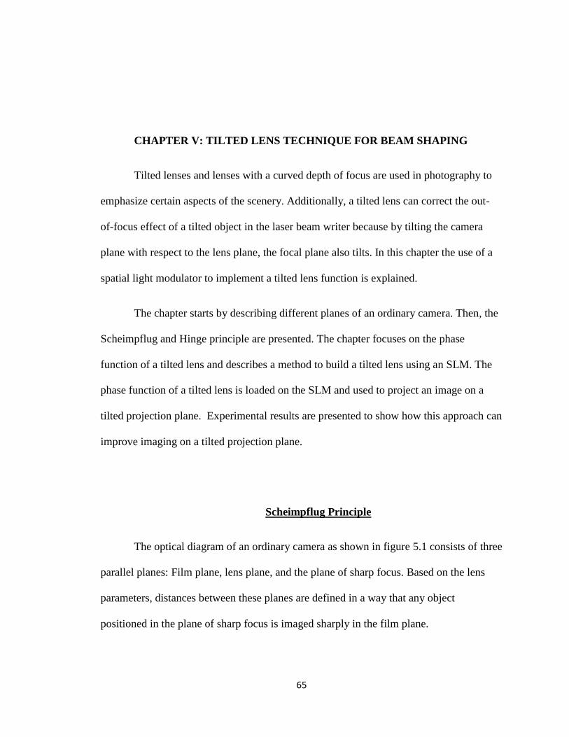
65
CHAPTER V: TILTED LENS TECHNIQUE FOR BEAM SHAPING
Tilted lenses and lenses with a curved depth of focus are used in photography to
emphasize certain aspects of the scenery. Additionally, a tilted lens can correct the out-
of-focus effect of a tilted object in the laser beam writer because by tilting the camera
plane with respect to the lens plane, the focal plane also tilts. In this chapter the use of a
spatial light modulator to implement a tilted lens function is explained.
The chapter starts by describing different planes of an ordinary camera. Then, the
Scheimpflug and Hinge principle are presented. The chapter focuses on the phase
function of a tilted lens and describes a method to build a tilted lens using an SLM. The
phase function of a tilted lens is loaded on the SLM and used to project an image on a
tilted projection plane. Experimental results are presented to show how this approach can
improve imaging on a tilted projection plane.
Scheimpflug Principle
The optical diagram of an ordinary camera as shown in figure 5.1 consists of three
parallel planes: Film plane, lens plane, and the plane of sharp focus. Based on the lens
parameters, distances between these planes are defined in a way that any object
positioned in the plane of sharp focus is imaged sharply in the film plane.
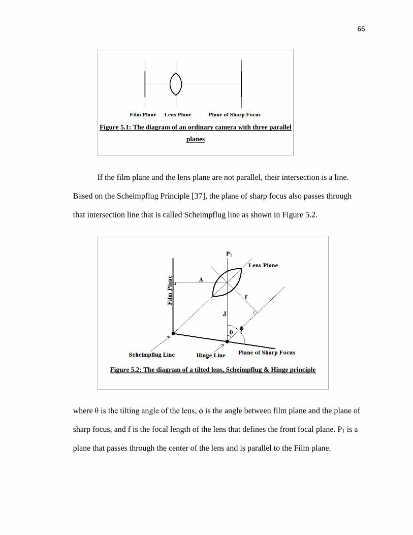
66
If the film plane and the lens plane are not parallel, their intersection is a line.
Based on the Scheimpflug Principle [37], the plane of sharp focus also passes through
that intersection line that is called Scheimpflug line as shown in Figure 5.2.
where θ is the tilting angle of the lens, ϕ is the angle between film plane and the plane of
sharp focus, and f is the focal length of the lens that defines the front focal plane. P1 is a
plane that passes through the center of the lens and is parallel to the Film plane.
Figure 5.2: The diagram of a tilted lens, Scheimpflug & Hinge principle
Figure 5.1: The diagram of an ordinary camera with three parallel
planes

67
The hinge rule states that P1, front focal plane, and the plane of sharp focus
intersect at a line called Hinge Line [37]. The Hinge rule is best understood by realizing
that the points on the Hinge line are conjugate to points in the Film plane at infinity since
they are at a distance of f from the lens. Based on the Hinge rule, knowing the film plane
and lens tilting angle, we can find the distance of the hinge line from the lens’ center (see
Fig. 5.2):
𝐽 =𝑓
sin 𝜃 (5 − 1)
The Scheimpflug principle also defines the relationship between the lens tilting
angle and the angle between film plane and the plane of sharp focus:
𝜙 = 90° + 𝑡𝑎𝑛−1 [𝑓
𝐴 sin 𝜃−
1
tan𝜃] (5 − 2)
where the distance between P1 and film plane, A, and the lens tilting angle, θ, and the lens
focal length, f, determine the angle between the plane of sharp focus and film plane, ϕ.
Combining the Hinge rule and Scheimpflug principle together, all geometrical
information about tilted lens imaging are found. Having A, f, and α; J, and ϕ can be
calculated from equation 5-1, 5-2. Knowing the film plane, J, and ϕ, the plane of sharp
focus can be defined.
To build the tilted lens function using a SLM the phase function of a tilted lens
should be known. For a spherical thin lens positioned in the x-y plane and for paraxial
rays, the phase shift introduced by the lens can be approximated by [31]:
𝜙(𝑥, 𝑦) = 𝜙0 −𝜋
𝜆𝑓[𝑥2 + 𝑦2] (5 − 3)
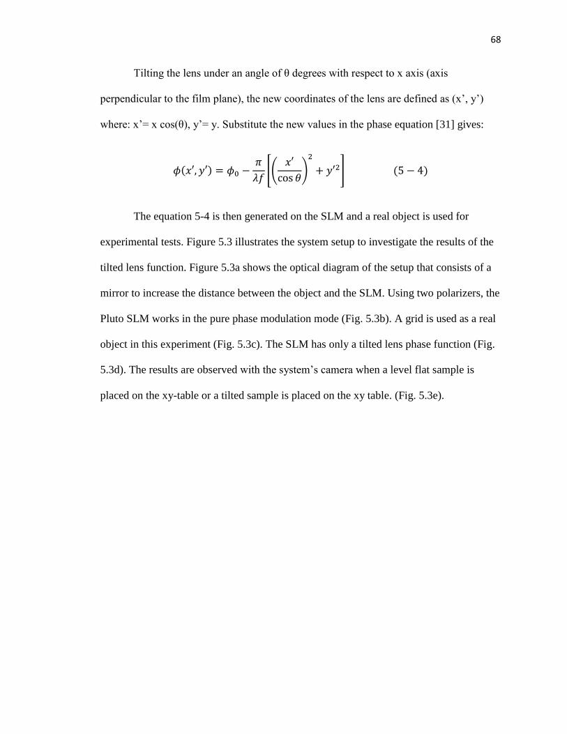
68
Tilting the lens under an angle of θ degrees with respect to x axis (axis
perpendicular to the film plane), the new coordinates of the lens are defined as (x’, y’)
where: x’= x cos(θ), y’= y. Substitute the new values in the phase equation [31] gives:
𝜙(𝑥′, 𝑦′) = 𝜙0 −𝜋
𝜆𝑓[(
𝑥′
cos 𝜃)
2
+ 𝑦′2] (5 − 4)
The equation 5-4 is then generated on the SLM and a real object is used for
experimental tests. Figure 5.3 illustrates the system setup to investigate the results of the
tilted lens function. Figure 5.3a shows the optical diagram of the setup that consists of a
mirror to increase the distance between the object and the SLM. Using two polarizers, the
Pluto SLM works in the pure phase modulation mode (Fig. 5.3b). A grid is used as a real
object in this experiment (Fig. 5.3c). The SLM has only a tilted lens phase function (Fig.
5.3d). The results are observed with the system’s camera when a level flat sample is
placed on the xy-table or a tilted sample is placed on the xy table. (Fig. 5.3e).
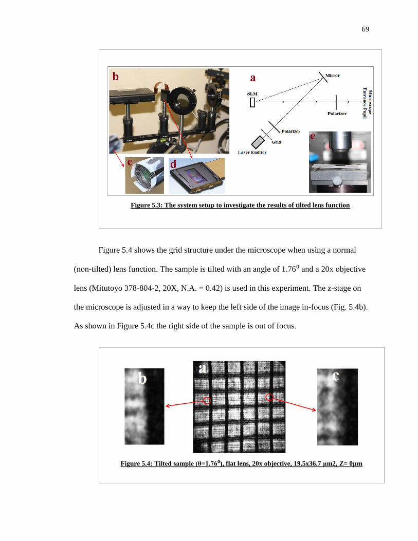
69
Figure 5.4 shows the grid structure under the microscope when using a normal
(non-tilted) lens function. The sample is tilted with an angle of 1.76⁰ and a 20x objective
lens (Mitutoyo 378-804-2, 20X, N.A. = 0.42) is used in this experiment. The z-stage on
the microscope is adjusted in a way to keep the left side of the image in-focus (Fig. 5.4b).
As shown in Figure 5.4c the right side of the sample is out of focus.
Figure 5.4: Tilted sample (θ=1.76⁰), flat lens, 20x objective, 19.5x36.7 μm2, Z= 0μm
Figure 5.3: The system setup to investigate the results of tilted lens function
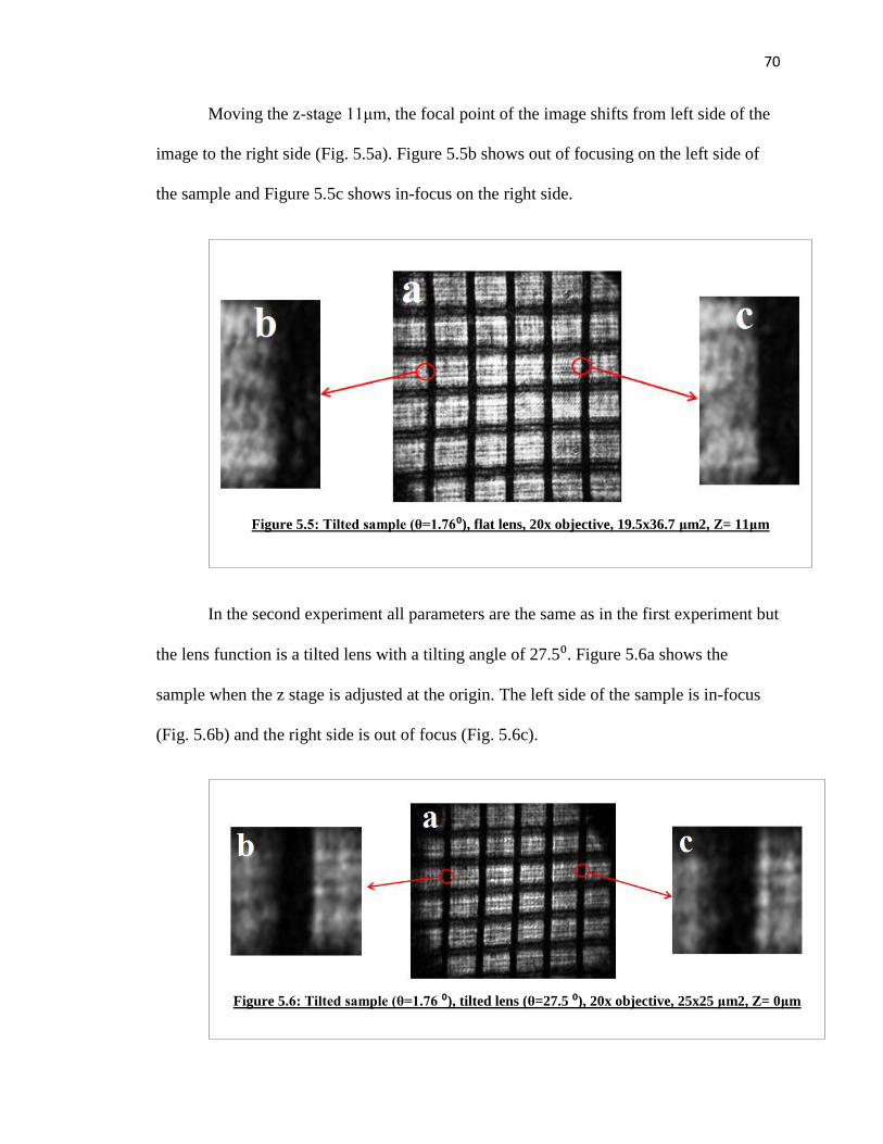
70
Moving the z-stage 11μm, the focal point of the image shifts from left side of the
image to the right side (Fig. 5.5a). Figure 5.5b shows out of focusing on the left side of
the sample and Figure 5.5c shows in-focus on the right side.
In the second experiment all parameters are the same as in the first experiment but
the lens function is a tilted lens with a tilting angle of 27.5⁰. Figure 5.6a shows the
sample when the z stage is adjusted at the origin. The left side of the sample is in-focus
(Fig. 5.6b) and the right side is out of focus (Fig. 5.6c).
Figure 5.6: Tilted sample (θ=1.76 ⁰), tilted lens (θ=27.5 ⁰), 20x objective, 25x25 μm2, Z= 0μm
Figure 5.5: Tilted sample (θ=1.76⁰), flat lens, 20x objective, 19.5x36.7 μm2, Z= 11μm
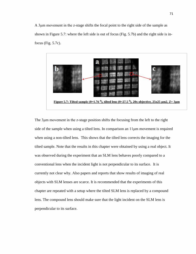
71
A 3μm movement in the z-stage shifts the focal point to the right side of the sample as
shown in Figure 5.7: where the left side is out of focus (Fig. 5.7b) and the right side is in-
focus (Fig. 5.7c).
The 3μm movement in the z-stage position shifts the focusing from the left to the right
side of the sample when using a tilted lens. In comparison an 11μm movement is required
when using a non-tilted lens. This shows that the tilted lens corrects the imaging for the
tilted sample. Note that the results in this chapter were obtained by using a real object. It
was observed during the experiment that an SLM lens behaves poorly compared to a
conventional lens when the incident light is not perpendicular to its surface. It is
currently not clear why. Also papers and reports that show results of imaging of real
objects with SLM lenses are scarce. It is recommended that the experiments of this
chapter are repeated with a setup where the tilted SLM lens is replaced by a compound
lens. The compound lens should make sure that the light incident on the SLM lens is
perpendicular to its surface.
Figure 5.7: Tilted sample (θ=1.76 ⁰), tilted lens (θ=27.5 ⁰), 20x objective, 25x25 μm2, Z= 3μm
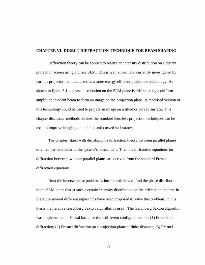
72
CHAPTER VI: DIRECT DIFFRACTION TECHNIQUE FOR BEAM SHAPING
Diffraction theory can be applied to realize an intensity distribution on a distant
projection screen using a phase SLM. This is well known and currently investigated by
various projector manufacturers as a more energy efficient projection technology. As
shown in figure 6.1, a phase distribution on the SLM plane is diffracted by a uniform
amplitude incident beam to form an image on the projection plane. A modified version of
this technology could be used to project an image on a tilted or curved surface. This
chapter discusses methods on how the standard lens-less projection techniques can be
used to improve imaging on inclined and curved susbstrates.
The chapter, starts with decribing the diffraction theory between parallel planes
oriented perpendicular to the system’s optical axis. Then the diffraction equations for
diffraction between two non-parallel planes are derived from the standard Fresnel
diffraction equations.
Next the inverse phase problem is introduced: how to find the phase distribution
in the SLM plane that creates a certain intensity distribution on the diffraction pattern. In
literature several different algorithms have been proposed to solve this problem. In this
thesis the iterative Gerchberg Saxton algorithm is used. The Gerchberg Saxton algorithm
was implemented in Visual basic for three different configurations i.e. (1) Fraunhofer
diffraction; (2) Fresnel diffraction on a projection plane at finite distance; (3) Fresnel
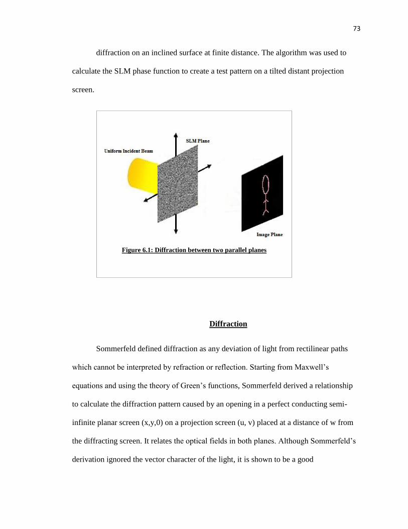
73
diffraction on an inclined surface at finite distance. The algorithm was used to
calculate the SLM phase function to create a test pattern on a tilted distant projection
screen.
Diffraction
Sommerfeld defined diffraction as any deviation of light from rectilinear paths
which cannot be interpreted by refraction or reflection. Starting from Maxwell’s
equations and using the theory of Green’s functions, Sommerfeld derived a relationship
to calculate the diffraction pattern caused by an opening in a perfect conducting semi-
infinite planar screen (x,y,0) on a projection screen (u, v) placed at a distance of w from
the diffracting screen. It relates the optical fields in both planes. Although Sommerfeld’s
derivation ignored the vector character of the light, it is shown to be a good
Figure 6.1: Diffraction between two parallel planes
74
approximation as long as the dimensions of the features on the planar diffracting screen
are much larger than the wavelength of the used light and the angles of light are small
compared to the optical axis of the system [39, 31].
Since the dimensions of a pixel of the SLM are approximately 30x larger than the
wavelength of the used light, the use of a scalar diffraction model is justified. Based on
the Rayleigh-Sommerfeld diffraction integral a distribution like E in the x-y plane is
diffracted into an electric field distribution Ed in the u-v plane (u,v) positioned at a
distance of w from the diffracting screen. If the projection screen is not perpendicular to
the optical axis of the system, w varies across the projection screen, and Ed is a function
of u, v, and w, as shown in Figure 6.2:
where:
Figure 6.2: Diffraction geometry
𝑟 = √(𝑥 − 𝑢)2 + (𝑦 − 𝑣)2 + 𝑧2
𝐸𝑑(𝑢, 𝑣, 𝑤) = 1
2𝜋∬𝐸(𝑥, 𝑦, 0) ×
𝑒−𝑖𝑘𝑟
𝑟×𝑧
𝑟× (𝑖𝑘 +
1
𝑟) 𝑑𝑥𝑑𝑦 (6 − 1)

75
This equation can be interpreted as the convolution of the impulse response of
free space with the input function E(x,y) [44]. One often considers the Rayleigh-
Sommerfeld diffraction integral to be superior over other diffraction theories such as
Huygens-Fresnel’s, and Kirchhoff’s theories. Although both are powerful and adequate
to describe the diffraction of the majority of problems these approximations are based on
incorrect assumptions about the boundary conditions for the electric and magnetic fields.
The Rayleigh-Sommerfeld integral can be simplified by making further
assumptions. In the far distance one can apply the following approximations for the
amplitude part of the expression: 𝑖𝑘 +1
𝑟≃ 𝑖𝑘 ,
𝑧
𝑟≃ 1. Furthermore the r in the phase part
of the equation can be approximated by: 𝑟 ≃ 𝑧 [1 +1
2(𝑥−𝑢
𝑧)2
+1
2(𝑦−𝑣
𝑧)2
]. Substituting
these new values in the Rayleigh-Sommerfeld integral gives:
which can be simplified to:
Substitute z→-z:
𝐸𝑑(𝑢, 𝑣, 𝑤) = 1
2𝜋∬𝐸(𝑥, 𝑦, 0) ×
𝑒−𝑖𝑘𝑧[1+
12(𝑥−𝑢𝑧)2+12(𝑦−𝑣𝑧)2]
𝑧×𝑧
𝑧× (𝑖𝑘 + 0)𝑑𝑥𝑑𝑦
𝐸𝑑(𝑢, 𝑣, 𝑤) = 𝑘𝑒𝑖𝑘𝑧
2𝑖𝜋𝑧∬𝐸(𝑥, 𝑦, 0) × 𝑒
𝑖𝜋𝜆𝑧[(𝑥−𝑢)2+(𝑦−𝑣)2]𝑑𝑥𝑑𝑦
(6 − 2)
(6 − 3)
(6 − 4)
𝐸𝑑(𝑢, 𝑣, 𝑤) = 𝑖𝑘𝑒−𝑖𝑘𝑧
2𝜋𝑧∬𝐸(𝑥, 𝑦, 0) × 𝑒
−𝑖𝑘2𝑧
[(𝑥−𝑢)2+(𝑦−𝑣)2]𝑑𝑥𝑑𝑦

76
which is presented in [31]. Expanding the exponential term inside the integral, for
diffraction between two parallel planes x-y and u-v as shown in image 6-2:
This equation is called the Fresnel diffraction integral. The inverse of equation (6-
5) is called the inverse Fresnel diffraction equation and is given by [47]:
𝐸(𝑥, 𝑦) = 𝑖𝑘𝑒−𝑖𝑘𝑧𝑒
−𝑖𝑘2𝑧(𝑥2+𝑦2)
2𝜋𝑧∬𝐸𝑑(𝑢, 𝑣)𝑒
−𝑖𝑘
2𝑧(𝑢2+𝑣2)𝑒
𝑖𝑘
2𝑧(2𝑢𝑥+2𝑣𝑦)𝑑𝑢𝑑𝑣
(6-5b)
Substituting Ed(u,v) in expression (6-5b) with expression (6-5) shows that the
integral on the right side of equation 6-5b is indeed E(x,y).
Note that the Fresnel diffraction equation, i.e. equation (6-5) contains a phase
factor in front of the integral and a phase factor under the integral. If one considers the
projection screen to be placed in infinity,
22 yxkz
and
2
22 vukz
, the
quadratic phase factors becomes small and it can be ignored. Therefore,
dxdyeyxEzi
kevuE
vyuxz
ikikz
d
222,
2,
The integral can be considered to be a scaled Fourier transform of the input
function E(x,y).
𝐸𝑑(𝑢, 𝑣) = 𝑘𝑒𝑖𝑘𝑧𝑒
𝑖𝑘2𝑧(𝑢2+𝑣2)
2𝑖𝜋𝑧∬𝐸(𝑥, 𝑦)𝑒
𝑖𝑘2𝑧(𝑥2+𝑦2)𝑒−
𝑖𝑘2𝑧(2𝑢𝑥+2𝑣𝑦)𝑑𝑥𝑑𝑦 (6 − 5)
(6 − 6)

77
Positioning a spherical lens with focal length f in front of the x-y plane as shown
in the image 6.3 and considering z=f have the same effect. The Fresnel diffraction
expression is simplified because of the phase function of the lens 𝑒−𝑖𝑘
2𝑓(𝑥2+𝑦2)
[31]:
This expression relates the optical field in the focal plane of the lens, Ed(u,v), to
the optical field in the input plane, E(x,y), of the setup. The factor in front of the integral
consists of a phase factor and constants. If one only considers the intensity of the image,
Figure 6.4: Positioning a spherical lens with focal length f in front of the x-y
plane to ignore the phase factors
Figure 6.3: Diffraction between two parallel planes
𝐸𝑑(𝑢, 𝑣)
= 𝑘𝑒𝑖𝑘𝑓𝑒
𝑖𝑘2𝑓(𝑢2+𝑣2)
2𝑖𝜋𝑓∬𝐸(𝑥, 𝑦)𝑒
−𝑖𝑘2𝑓(2𝑢𝑥+2𝑣𝑦)
𝑑𝑥𝑑𝑦 (6 − 7)

78
the phase factor is not relevant. The integral in the equation above is known as a 2-
Dimensional Fourier Transform. Therefore one often refers to the setup of Fig. 5-3 as a 1f
Fourier transform optical system. Introducing the spatial frequencies 𝑢′ = 𝑘𝑢
𝑓 , 𝑣′ = 𝑘
𝑣
𝑓
above equation can be written as:
𝐸𝑑(𝑢′, 𝑣′) = 𝑘𝑒𝑖𝑘𝑓𝑒
𝑖𝑓2𝑘(𝑢′2+𝑣′2)
2𝑖𝜋𝑓ℑ(𝐸(𝑥, 𝑦))
This is called the Fraunhofer diffraction integral.
The Fourier integral can be separated into two 1-D Fourier integrals. This
significantly speeds up the calculations. So, in discrete mode, one can take two 1-D Fast
Fourier Transform (FFT) instead of a 2-D Discrete Fourier Transform (DFT):
The input function E(x,y) of the setup can be realized by shining a parallel laser
beam on a mask or a spatial light modulator. Both the amplitude and the phase, or just the
amplitude or the phase of the input optical field can be modulated. Various SLM
𝐸𝑑(𝑢, 𝑦) = 𝑘𝑒𝑖𝑘𝑓𝑒
𝑖𝑘2𝑓𝑢2
2𝑖𝜋𝑓∫𝐸(𝑥, 𝑦)𝑒
−𝑖𝑘𝑢𝑥𝑓 𝑑𝑥
𝐸𝑑(𝑢, 𝑣) = 𝑒𝑖𝑘2𝑓𝑣2∫𝐸(𝑢, 𝑦)𝑒
−𝑖𝑘𝑣𝑦𝑓 𝑑𝑦
𝐸𝑑(𝑢, 𝑣) = 𝑘𝑒𝑖𝑘𝑓𝑒
𝑖𝑘2𝑓(𝑢2+𝑣2)
2𝑖𝜋𝑓∬𝐸(𝑥, 𝑦)𝑒
−𝑖𝑘2𝑓(2𝑢𝑥+2𝑣𝑦)
𝑑𝑥𝑑𝑦
(6 − 8)
(6 − 9)
(6 − 10)
(6 − 11)
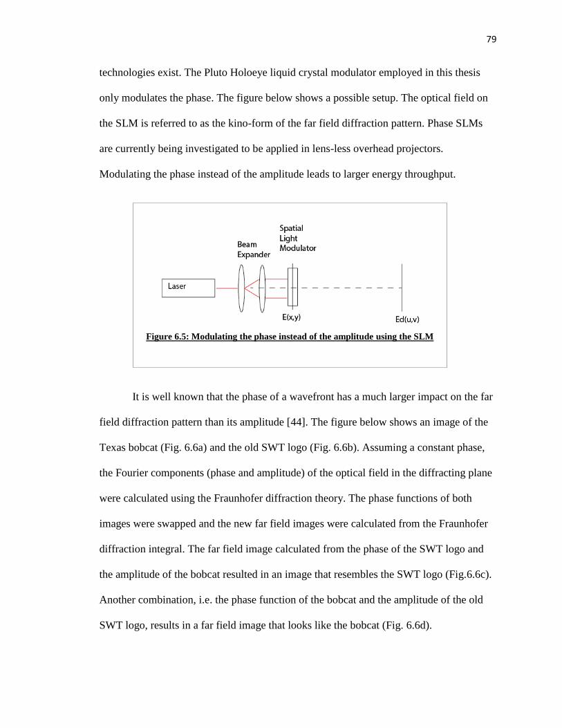
79
technologies exist. The Pluto Holoeye liquid crystal modulator employed in this thesis
only modulates the phase. The figure below shows a possible setup. The optical field on
the SLM is referred to as the kino-form of the far field diffraction pattern. Phase SLMs
are currently being investigated to be applied in lens-less overhead projectors.
Modulating the phase instead of the amplitude leads to larger energy throughput.
It is well known that the phase of a wavefront has a much larger impact on the far
field diffraction pattern than its amplitude [44]. The figure below shows an image of the
Texas bobcat (Fig. 6.6a) and the old SWT logo (Fig. 6.6b). Assuming a constant phase,
the Fourier components (phase and amplitude) of the optical field in the diffracting plane
were calculated using the Fraunhofer diffraction theory. The phase functions of both
images were swapped and the new far field images were calculated from the Fraunhofer
diffraction integral. The far field image calculated from the phase of the SWT logo and
the amplitude of the bobcat resulted in an image that resembles the SWT logo (Fig.6.6c).
Another combination, i.e. the phase function of the bobcat and the amplitude of the old
SWT logo, results in a far field image that looks like the bobcat (Fig. 6.6d).
Figure 6.5: Modulating the phase instead of the amplitude using the SLM
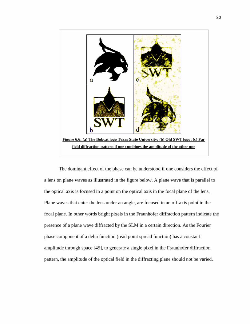
80
The dominant effect of the phase can be understood if one considers the effect of
a lens on plane waves as illustrated in the figure below. A plane wave that is parallel to
the optical axis is focused in a point on the optical axis in the focal plane of the lens.
Plane waves that enter the lens under an angle, are focused in an off-axis point in the
focal plane. In other words bright pixels in the Fraunhofer diffraction pattern indicate the
presence of a plane wave diffracted by the SLM in a certain direction. As the Fourier
phase component of a delta function (read point spread function) has a constant
amplitude through space [45], to generate a single pixel in the Fraunhofer diffraction
pattern, the amplitude of the optical field in the diffracting plane should not be varied.
Figure 6.6: (a) The Bobcat logo Texas State University; (b) Old SWT logo; (c) Far
field diffraction pattern if one combines the amplitude of the other one
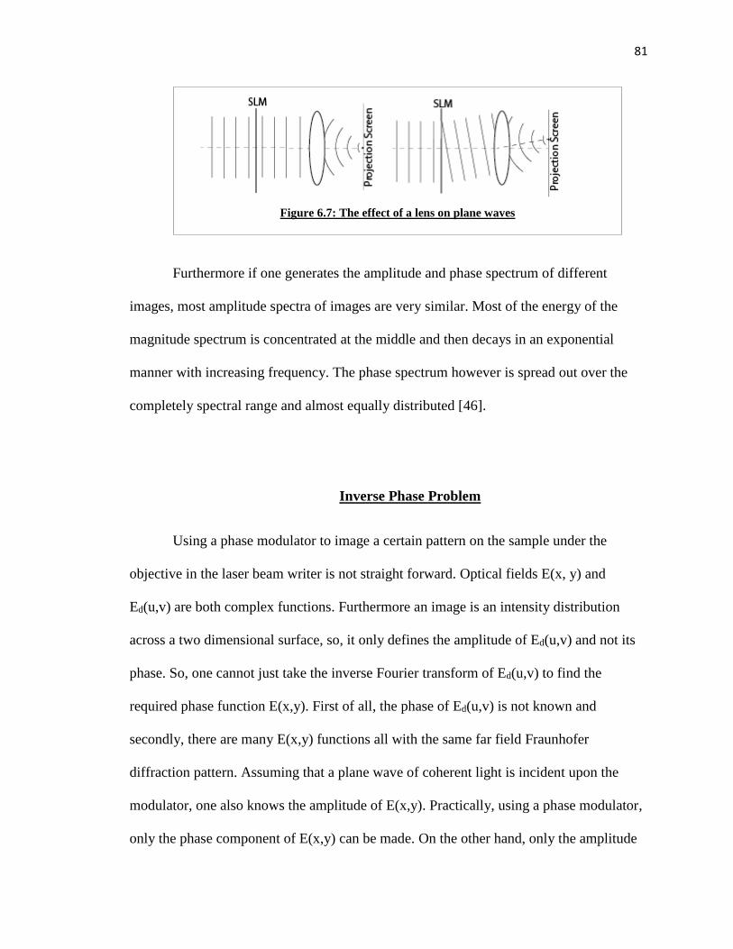
81
Furthermore if one generates the amplitude and phase spectrum of different
images, most amplitude spectra of images are very similar. Most of the energy of the
magnitude spectrum is concentrated at the middle and then decays in an exponential
manner with increasing frequency. The phase spectrum however is spread out over the
completely spectral range and almost equally distributed [46].
Inverse Phase Problem
Using a phase modulator to image a certain pattern on the sample under the
objective in the laser beam writer is not straight forward. Optical fields E(x, y) and
Ed(u,v) are both complex functions. Furthermore an image is an intensity distribution
across a two dimensional surface, so, it only defines the amplitude of Ed(u,v) and not its
phase. So, one cannot just take the inverse Fourier transform of Ed(u,v) to find the
required phase function E(x,y). First of all, the phase of Ed(u,v) is not known and
secondly, there are many E(x,y) functions all with the same far field Fraunhofer
diffraction pattern. Assuming that a plane wave of coherent light is incident upon the
modulator, one also knows the amplitude of E(x,y). Practically, using a phase modulator,
only the phase component of E(x,y) can be made. On the other hand, only the amplitude
Figure 6.7: The effect of a lens on plane waves
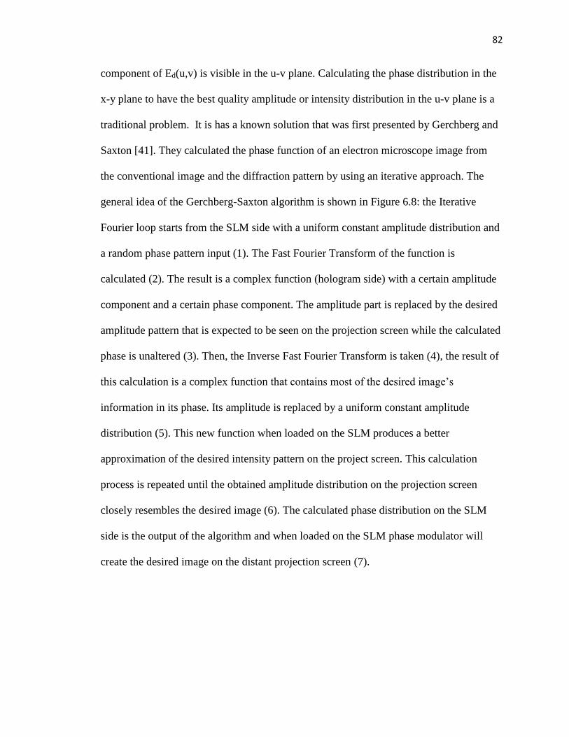
82
component of Ed(u,v) is visible in the u-v plane. Calculating the phase distribution in the
x-y plane to have the best quality amplitude or intensity distribution in the u-v plane is a
traditional problem. It is has a known solution that was first presented by Gerchberg and
Saxton [41]. They calculated the phase function of an electron microscope image from
the conventional image and the diffraction pattern by using an iterative approach. The
general idea of the Gerchberg-Saxton algorithm is shown in Figure 6.8: the Iterative
Fourier loop starts from the SLM side with a uniform constant amplitude distribution and
a random phase pattern input (1). The Fast Fourier Transform of the function is
calculated (2). The result is a complex function (hologram side) with a certain amplitude
component and a certain phase component. The amplitude part is replaced by the desired
amplitude pattern that is expected to be seen on the projection screen while the calculated
phase is unaltered (3). Then, the Inverse Fast Fourier Transform is taken (4), the result of
this calculation is a complex function that contains most of the desired image’s
information in its phase. Its amplitude is replaced by a uniform constant amplitude
distribution (5). This new function when loaded on the SLM produces a better
approximation of the desired intensity pattern on the project screen. This calculation
process is repeated until the obtained amplitude distribution on the projection screen
closely resembles the desired image (6). The calculated phase distribution on the SLM
side is the output of the algorithm and when loaded on the SLM phase modulator will
create the desired image on the distant projection screen (7).
83
It can be proved that the sum of the squared differences between the pixel’s
amplitude in the Hologram or SLM planes and the amplitudes of the perfect images
decreases after each iterative loop [43]. The algorithm converges and the estimated image
as defined in the algorithm, becomes more similar to the desired pattern. Image 6.9 shows
the simulation result of Gerchberg-Saxton algorithm performed by Visual Basic. The
calculated holograms images are shown after 2, 10, and 20 loops.
Figure 6.8: Gerchberg-Saxton algorithm diagram
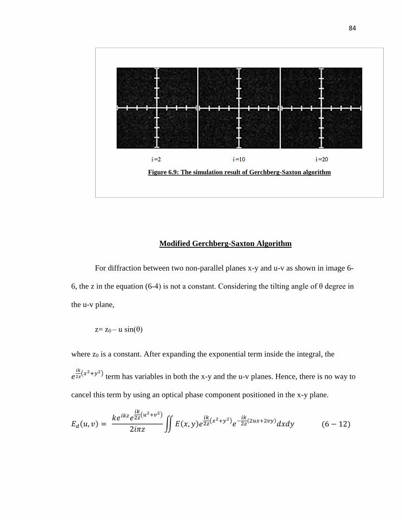
84
Modified Gerchberg-Saxton Algorithm
For diffraction between two non-parallel planes x-y and u-v as shown in image 6-
6, the z in the equation (6-4) is not a constant. Considering the tilting angle of θ degree in
the u-v plane,
z= z0 – u sin(θ)
where z0 is a constant. After expanding the exponential term inside the integral, the
𝑒𝑖𝑘
2𝑧(𝑥2+𝑦2)
term has variables in both the x-y and the u-v planes. Hence, there is no way to
cancel this term by using an optical phase component positioned in the x-y plane.
𝐸𝑑(𝑢, 𝑣) = 𝑘𝑒𝑖𝑘𝑧𝑒
𝑖𝑘2𝑧(𝑢2+𝑣2)
2𝑖𝜋𝑧∬𝐸(𝑥, 𝑦)𝑒
𝑖𝑘2𝑧(𝑥2+𝑦2)𝑒−
𝑖𝑘2𝑧(2𝑢𝑥+2𝑣𝑦)𝑑𝑥𝑑𝑦
Figure 6.9: The simulation result of Gerchberg-Saxton algorithm
(6 − 12)
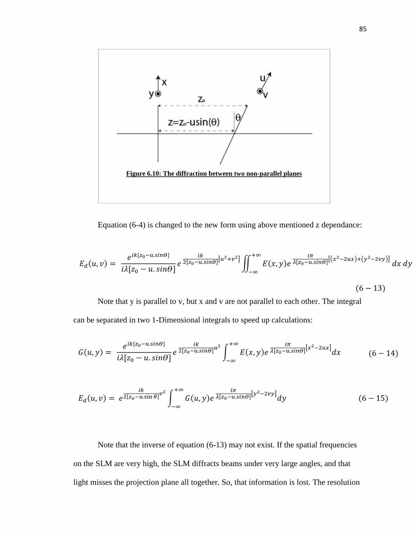
85
Equation (6-4) is changed to the new form using above mentioned z dependance:
Note that y is parallel to v, but x and v are not parallel to each other. The integral
can be separated in two 1-Dimensional integrals to speed up calculations:
Note that the inverse of equation (6-13) may not exist. If the spatial frequencies
on the SLM are very high, the SLM diffracts beams under very large angles, and that
light misses the projection plane all together. So, that information is lost. The resolution
Figure 6.10: The diffraction between two non-parallel planes
𝐺(𝑢, 𝑦) = 𝑒𝑖𝑘[𝑧0−𝑢.𝑠𝑖𝑛𝛳]
𝑖𝜆[𝑧0 − 𝑢. 𝑠𝑖𝑛𝛳]𝑒
𝑖𝑘
2[𝑧0−𝑢.𝑠𝑖𝑛𝛳]𝑢2
∫ 𝐸(𝑥, 𝑦)𝑒
𝑖𝜋𝜆[𝑧0−𝑢.𝑠𝑖𝑛𝛳]
[𝑥2−2𝑢𝑥]𝑑𝑥
+∞
−∞
𝐸𝑑(𝑢, 𝑣) = 𝑒𝑖𝑘
2[𝑧𝑜−𝑢.sin𝜃]𝑣2
∫ 𝐺(𝑢, 𝑦)𝑒
𝑖𝜋𝜆[𝑧0−𝑢.𝑠𝑖𝑛𝛳]
[𝑦2−2𝑣𝑦]𝑑𝑦
+∞
−∞
𝐸𝑑(𝑢, 𝑣) = 𝑒𝑖𝑘[𝑧0−𝑢.𝑠𝑖𝑛𝛳]
𝑖𝜆[𝑧0 − 𝑢. 𝑠𝑖𝑛𝛳]𝑒
𝑖𝑘
2[𝑧0−𝑢.𝑠𝑖𝑛𝛳][𝑢2+𝑣2]
∬ 𝐸(𝑥, 𝑦)𝑒
𝑖𝜋𝜆[𝑧0−𝑢.𝑠𝑖𝑛𝛳]
[(𝑥2−2𝑢𝑥)+(𝑦2−2𝑣𝑦)] 𝑑𝑥 𝑑𝑦
+∞
−∞
(6 − 13)
(6 − 14)
(6 − 15)
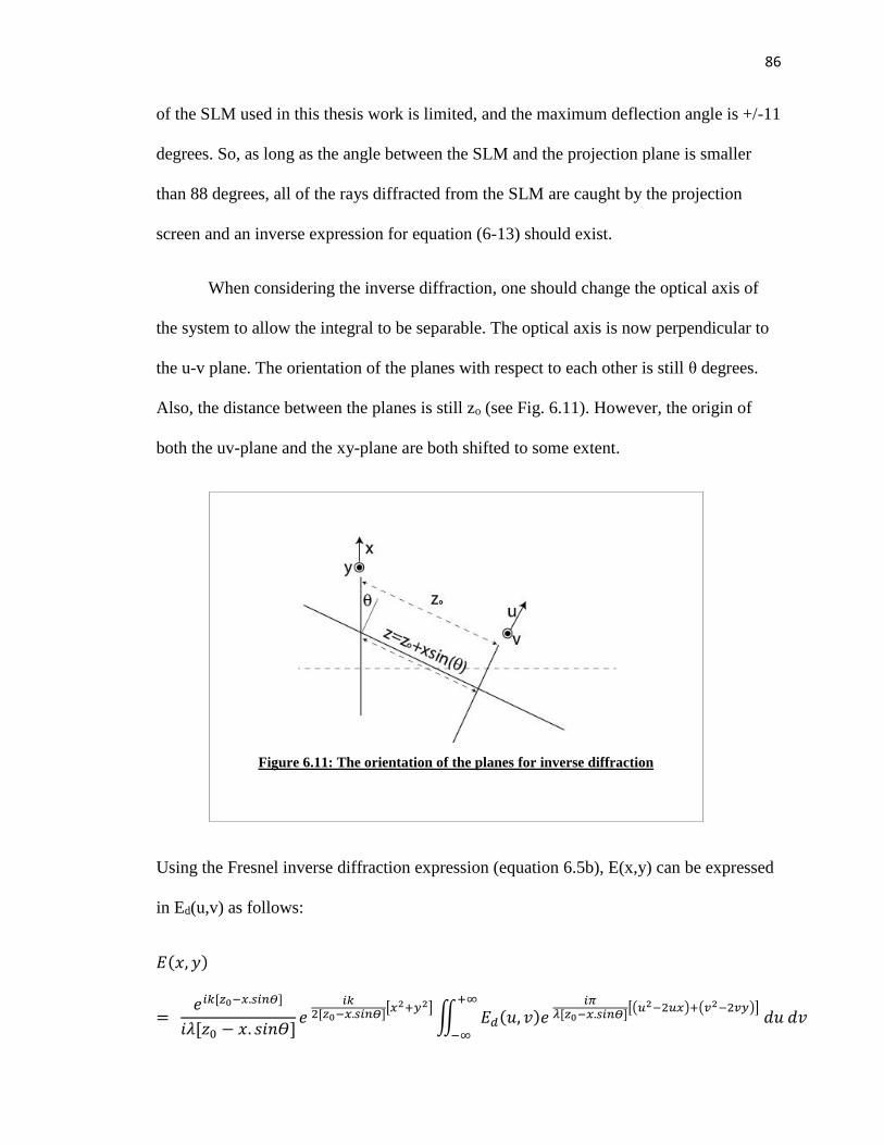
86
of the SLM used in this thesis work is limited, and the maximum deflection angle is +/-11
degrees. So, as long as the angle between the SLM and the projection plane is smaller
than 88 degrees, all of the rays diffracted from the SLM are caught by the projection
screen and an inverse expression for equation (6-13) should exist.
When considering the inverse diffraction, one should change the optical axis of
the system to allow the integral to be separable. The optical axis is now perpendicular to
the u-v plane. The orientation of the planes with respect to each other is still θ degrees.
Also, the distance between the planes is still zo (see Fig. 6.11). However, the origin of
both the uv-plane and the xy-plane are both shifted to some extent.
Using the Fresnel inverse diffraction expression (equation 6.5b), E(x,y) can be expressed
in Ed(u,v) as follows:
𝐸(𝑥, 𝑦)
= 𝑒𝑖𝑘[𝑧0−𝑥.𝑠𝑖𝑛𝛳]
𝑖𝜆[𝑧0 − 𝑥. 𝑠𝑖𝑛𝛳]𝑒
𝑖𝑘
2[𝑧0−𝑥.𝑠𝑖𝑛𝛳][𝑥2+𝑦2]
∬ 𝐸𝑑(𝑢, 𝑣)𝑒
𝑖𝜋𝜆[𝑧0−𝑥.𝑠𝑖𝑛𝛳]
[(𝑢2−2𝑢𝑥)+(𝑣2−2𝑣𝑦)] 𝑑𝑢 𝑑𝑣
+∞
−∞
Figure 6.11: The orientation of the planes for inverse diffraction

87
(6-16)
Note that this integral can also be separated in two 1-Dimensional integrals:
Note that the xy-coordinate system of equations (6-16), (6-17) and (6-18) is different
from the xy-coordinate system of equations (6-13), (6-14), and (6-15). This is also clear
from comparing figures 6.9 and 6.10. The origin of the xy-coordinate system of figure
6.10 is shifted up with respect to the origin of figure 6.9’s xy-coordinate system’s origin.
Discrete Mode Calculations
To calculate the transfer function for any distributions using a processor, all relations
should be changed into discrete mode. G (u, y) as defined in equation 6-14 has an integral
in general form of:
where a= λz0 and b= -λ sin θ are constants inside the integral, and K1 contains the terms
in front of the integral of equation (6-14). Ed (u, y) as defined on equation 6-15 has an
integral in general form of:
𝐺(𝑢, 𝑦) = 𝐾1∫ 𝐸(𝑥, 𝑦)𝑒 𝑖𝜋
𝑎+𝑏𝑢[𝑥2−2𝑢𝑥]𝑑𝑥
+∞
−∞
(6 − 19)
𝐸𝑑(𝑢, 𝑣) = 𝐾2∫ 𝐺(𝑢, 𝑦)𝑒 𝑖𝜋𝑐[𝑦2−2𝑣𝑦]𝑑𝑦
+∞
−∞
(6 − 20)
𝐺𝑑(𝑥, 𝑣) = 𝑒−𝑖𝑘[𝑧0−𝑥.𝑠𝑖𝑛𝛳]
𝑖𝜆[𝑧0 − 𝑥. 𝑠𝑖𝑛𝛳]𝑒
−𝑖𝑘
2[𝑧0−𝑥.𝑠𝑖𝑛𝛳]𝑥2
∫ 𝐸𝑑(𝑢, 𝑣)𝑒
−𝑖𝜋𝜆[𝑧0−𝑥.𝑠𝑖𝑛𝛳]
[𝑢2−2𝑢𝑥]𝑑𝑢
+∞
−∞
𝐸(𝑥, 𝑦) = 𝑒
−𝑖𝑘2[𝑧0−𝑥.𝑠𝑖𝑛𝛳]
𝑦2
∫ 𝐺𝑑(𝑥, 𝑣)𝑒
−𝑖𝜋𝜆[𝑧0−𝑥.𝑠𝑖𝑛𝛳]
[𝑣2−2𝑣𝑦]𝑑𝑣
+∞
−∞
(6 − 17)
(6 − 18)
88
where c= λ [z0-u.sin θ] is a constant inside the integral and K2 contains the terms in front
of the integral of equation (5-15). As the SLM has finite dimensions, E(x,y) is zero
outside the optical aperture of the system. So, the infinite boundaries can be replaced by
finite boundaries. Also, E(x,y) is not continuous because the SLM is a digital device. So,
E(x,y) is pixilated. Assuming that the SLM has Nx’ pixels in the x-direction and Ny’
pixels in the y-direction and assuming that the pixels size to be square equal to PS, the
pixelated version of E, E’, can be written as:
PSyyPSxxrectPSyPSxEyxEx yN
y
N
x
',' ',')','('1
0'
1
0'
' '
which shows that the pixelated version is the convolution of E with the rectangular
function, where the rectangular function is defined as:
yPSyxPSx
PSyPSxyxrect
,0 , ,0 0
0 ,0 1),(
Assuming that the effect of pixelation is negligible, the rect function can be replaced in
above equation by 1. This corresponds to assuming that each pixel is described by a delta
function.
E(x,y) is sampled Nx’ Ny’ times within the dimensions of the SLM, i.e. 𝑁𝑥′𝑃𝑆 × 𝑁𝑦′𝑃𝑆.
Note that based on Nyquist sampling theorem, 1/PS must be twice the highest spatial
frequency in E(x,y). In other words the SLM can only be used to make spatial
frequencies up to 1/(2*PS). Higher spatial frequencies (read higher diffracted beams)
cannot be created by the SLM. Rewriting equation 6.14 and 6.15, gives for the diffraction
equations:
𝐸′𝑑(𝑚, 𝑛) = 𝐾2𝑃𝑆∑ 𝐺′(𝑚, 𝑦′)𝑒 𝑖𝜋
𝑐[(𝑦′𝑃𝑆)
2−2𝑦′𝑃𝑆𝑛∆𝑣]𝑁𝑦′−1
𝑦′=0
𝑚 = 0, 1,… , (𝑁𝑢 − 1), 𝑛 = 0, 1, … , (𝑁𝑣 − 1)
(6 − 21)
(6 − 22)
𝐺′(𝑚, 𝑦′) = 𝐾1𝑃𝑆 ∑ 𝐸′(𝑥′, 𝑦′)𝑒 𝑖𝜋
𝑎+𝑏𝑚∆𝑢[(𝑥′𝑃𝑆)2−2𝑥′𝑃𝑆𝑚∆𝑢]
𝑁𝑥′−1
𝑥′=0
𝑚 = 0, 1,… , (𝑁𝑢 − 1)
(6 − 23)
(6 − 24)
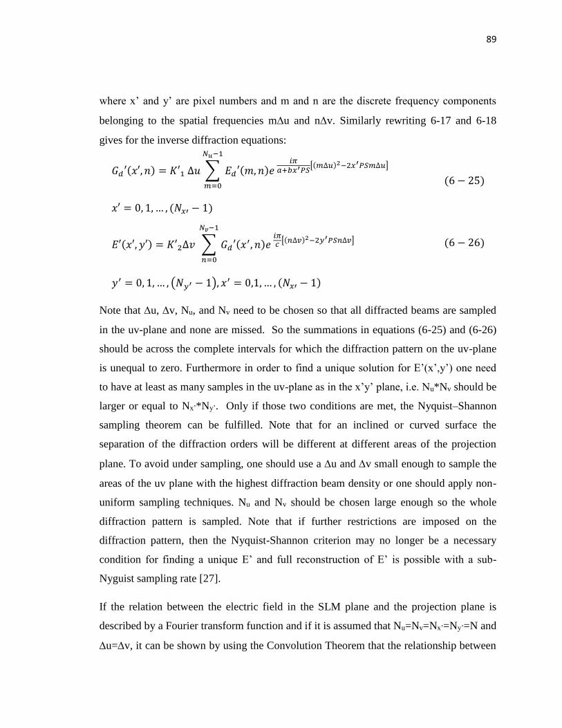
89
where x’ and y’ are pixel numbers and m and n are the discrete frequency components
belonging to the spatial frequencies mu and nv. Similarly rewriting 6-17 and 6-18
gives for the inverse diffraction equations:
Note that u, v, Nu, and Nv need to be chosen so that all diffracted beams are sampled
in the uv-plane and none are missed. So the summations in equations (6-25) and (6-26)
should be across the complete intervals for which the diffraction pattern on the uv-plane
is unequal to zero. Furthermore in order to find a unique solution for E’(x’,y’) one need
to have at least as many samples in the uv-plane as in the x’y’ plane, i.e. Nu*Nv should be
larger or equal to Nx’*Ny’. Only if those two conditions are met, the Nyquist–Shannon
sampling theorem can be fulfilled. Note that for an inclined or curved surface the
separation of the diffraction orders will be different at different areas of the projection
plane. To avoid under sampling, one should use a u and v small enough to sample the
areas of the uv plane with the highest diffraction beam density or one should apply non-
uniform sampling techniques. Nu and Nv should be chosen large enough so the whole
diffraction pattern is sampled. Note that if further restrictions are imposed on the
diffraction pattern, then the Nyquist-Shannon criterion may no longer be a necessary
condition for finding a unique E’ and full reconstruction of E’ is possible with a sub-
Nyguist sampling rate [27].
If the relation between the electric field in the SLM plane and the projection plane is
described by a Fourier transform function and if it is assumed that Nu=Nv=Nx’=Ny’=N and
u=v, it can be shown by using the Convolution Theorem that the relationship between
𝐸′(𝑥′, 𝑦′) = 𝐾′2∆𝑣 ∑ 𝐺𝑑′(𝑥′, 𝑛)𝑒
𝑖𝜋𝑐[(𝑛∆𝑣)2−2𝑦′𝑃𝑆𝑛∆𝑣]
𝑁𝑣−1
𝑛=0
𝑦′ = 0, 1, … , (𝑁𝑦′ − 1), 𝑥′ = 0,1, … , (𝑁𝑥′ − 1)
(6 − 26)
𝐺𝑑′(𝑥′, 𝑛) = 𝐾′1 ∆𝑢 ∑ 𝐸𝑑′(𝑚, 𝑛)𝑒
𝑖𝜋𝑎+𝑏𝑥′𝑃𝑆
[(𝑚∆𝑢)2−2𝑥′𝑃𝑆𝑚∆𝑢]
𝑁𝑢−1
𝑚=0
𝑥′ = 0, 1, … , (𝑁𝑥′ − 1)
(6 − 25)
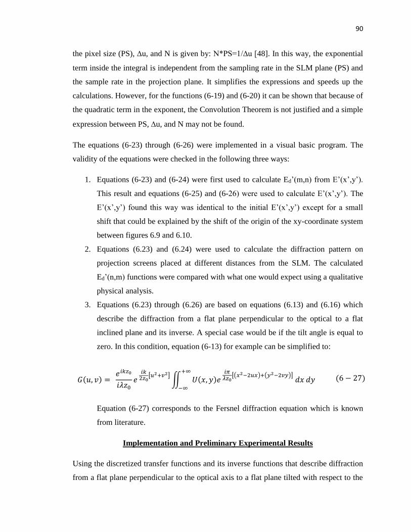
90
the pixel size (PS), u, and N is given by: N*PS=1/∆u [48]. In this way, the exponential
term inside the integral is independent from the sampling rate in the SLM plane (PS) and
the sample rate in the projection plane. It simplifies the expressions and speeds up the
calculations. However, for the functions (6-19) and (6-20) it can be shown that because of
the quadratic term in the exponent, the Convolution Theorem is not justified and a simple
expression between PS, u, and N may not be found.
The equations (6-23) through (6-26) were implemented in a visual basic program. The
validity of the equations were checked in the following three ways:
1. Equations (6-23) and (6-24) were first used to calculate Ed’(m,n) from E’(x’,y’).
This result and equations (6-25) and (6-26) were used to calculate E’(x’,y’). The
E’(x’,y’) found this way was identical to the initial E’(x’,y’) except for a small
shift that could be explained by the shift of the origin of the xy-coordinate system
between figures 6.9 and 6.10.
2. Equations (6.23) and (6.24) were used to calculate the diffraction pattern on
projection screens placed at different distances from the SLM. The calculated
Ed’(n,m) functions were compared with what one would expect using a qualitative
physical analysis.
3. Equations (6.23) through (6.26) are based on equations (6.13) and (6.16) which
describe the diffraction from a flat plane perpendicular to the optical to a flat
inclined plane and its inverse. A special case would be if the tilt angle is equal to
zero. In this condition, equation (6-13) for example can be simplified to:
Equation (6-27) corresponds to the Fersnel diffraction equation which is known
from literature.
Implementation and Preliminary Experimental Results
Using the discretized transfer functions and its inverse functions that describe diffraction
from a flat plane perpendicular to the optical axis to a flat plane tilted with respect to the
𝐺(𝑢, 𝑣) = 𝑒𝑖𝑘𝑧0
𝑖𝜆𝑧0𝑒
𝑖𝑘2𝑧0
[𝑢2+𝑣2]∬ 𝑈(𝑥, 𝑦)𝑒
𝑖𝜋𝜆𝑧0
[(𝑥2−2𝑢𝑥)+(𝑦2−2𝑣𝑦)] 𝑑𝑥 𝑑𝑦
+∞
−∞
(6 − 27)
91
optical axis (equations 6-23, 6-24, 6-25, and 6-26), the modified Gerchberg-Saxton
algorithm for diffraction on a tilted projection screen (Fig. 6.12) was implemented in a
visual basic program.
The modified Gerchberg-Saxton visual basic program was used to calculate the phase
pattern to create various test patterns on an inclined projection screen. The algorithm
appeared to be stable and converging rapidly for all patterns the algorithm was tested
with. Some preliminary results are shown in Figure 6.13 for a simple xy-coordinate
system on a black background. The images show the estimated diffraction pattern using
the optical field that was found after 2 iterations, after 10 iterations, and after 20
iterations.
Figure 6.12: The modified Gerchberg-Saxton algorithm diagram
92
The PLUTO SLM setup was used to project the calculated SLM optical field using the
modified Gerchberg Saxton algorithm on a screen tilted with the optical axis. The screen
was oriented at 41ͦ and located at 60 cm from the SLM. The images shown in Figure 6.14
are taken from the screen using a Canon DSLR camera. Figure 6.14a shows the projected
pattern on the screen when the SLM was loaded with the optical field calculated using the
normal Gerchberg Saxton algorithm. Figure 6.14c shows that the left of the image is out
of focus while Figure 6.14d shows that the right side of the image is in-focus. In the
second experiment the SLM was loaded with the optical field that was calculated using
the modified Gerchberg Saxton algorithm (θ=41ͦ). Results are shown on Figure 6.14b.
Figures 6.14e and 6.13f show that the projected image is in focus on both the left and the
right sides of the image and that a small improvement is obtained. The results of Figure
6.14 also show that if the SLM is loaded with the results of the modified Gerchberg
Saxtan algorithm, the diffraction pattern on an inclined distant screen resembles the
pattern that was used as input of the modified Gerchberg-Saxtan algorithm. So this
furthermore provides some verification of equations 6-23 through 6-26.
Figure 6.13: Simulation result of Modified Gerchberg Saxton algorithm
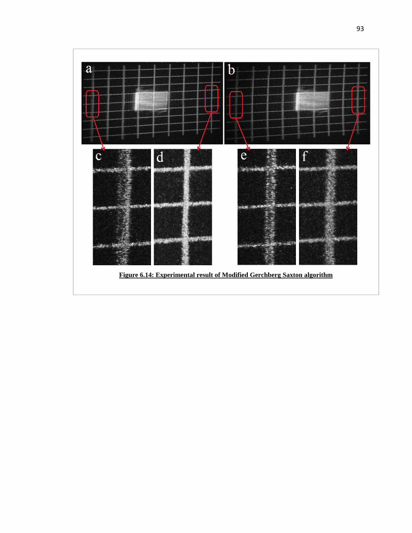
93
Figure 6.14: Experimental result of Modified Gerchberg Saxton algorithm
94
CHAPTER VII: CONCLUSION AND RECOMMENDATION FOR FURTHER
RESEARCH
Three different techniques were studied in this thesis to shape the laser beam for
lithography on curved surfaces using the Holoeye Pluto phase only modulator and the
Holoeye LC 2002 twisted nematic modulator.
Limitations on beam shaping, focusing, and imaging using SLM single lenses and
SLM multi-lens arrays were defined in terms of optical aberrations, pixel size, SLM size,
and SLM modulation depth. In addition to the classical lens aberrations, SLM lenses have
three additional contributions to the optical aberration, i.e. effects of quantization, effect
of pixelation, and effect of the curvature of the modulator. Although the effect of
pixelation can be minimized by choosing an SLM with a small pixel size, theoretically it
cannot be nullified as strictly speaking the Shannon-Nyguist sampling condition cannot
be fulfilled for a quadratic phase function. Quantization aberration has a significant
effect on the center of the lens while the effect of pixelation increases near the lens edges.
Small diameter lenses with a large focal distance implemented on the SLM have a small
pixelation aberration but they are diffraction limited. Large diameter lenses implemented
on the SLM have a negligible diffraction but a large pixelation aberration and their
performance is aberration limited. Preliminary experiments that explored the use of an
SLM multi lens array whose lenses have different focal distances to improve the depth of
focus and image quality for imaging on a curved substrate with detailed surface
95
topography is disappointing. But, for tilted substrates or for samples that are
approximated by several simple step functions, the multi lens approach provides a
qualitative improvement. More work is necessary including the introduction of a
quantitative measurement method to describe image quality on tilted and curved
substrates.
An expression for the phase function of a tilted lens was derived and implemented
on the SLM to improve the imaging quality on a tilted surface. This approach requires a
real object that is imaged by the SLM lens on the tilted plane. Experimental results show
a small improvement. The experiments also showed that the imaging capabilities of an
SLM lens are poor when light incident on the SLM is not perpendicular. It is
recommended that the tilted lens functions are repeated by designing a compound lens
consisting of a tilted SLM lens and one or more standard glass lenses. The design of the
compound lens should place the SLM in infinity space, to make sure that light on the
SLM is perpendicular to it.
An expression that describes the diffraction from a flat plane perpendicular to the
optical axis to a flat plane tilted with respect to the optical axis were derived from the
Rayleigh-Sommerfeld diffraction integrals. Also an expression for the inverse function
was derived. Both diffraction equations were digitized and could be separated into two 1
dimensional summations significantly reducing the calculation time compared to a
straight forward 2D DFT calculation. It was not possible to use FFT for the summations.
The derived expressions were used to implement the modified Gerchberg-Saxton
algorithm. Preliminary experiments using a simple test pattern show that the SLM optical
field calculated with this modified Gerchberg-Saxton does allow for projection on tilted
96
screens. The algorithm seems to converge and is stable for various test patterns. A similar
approach may be used for diffraction from a planar surface to a known curved surface.
The modified Gerchberg-Saxton algorithm is more time consuming than the classical
Fraunhofer based Gerchberg-Saxton algorithm as one cannot use the FFT algorithm for
the former. Although the derivations in chapter 6 show that it is not possible to write the
diffraction between two non-parallel planes as a single Fourier transform, it is possible to
write it as a Fourier transform (calculation of the diffracted beams), followed by a
translation (propagation of the diffracted beams through space), followed by an inverse
Fourier transform (reconstruction of the optical field on the inclined diffraction pattern).
Using such approach one should be able to use the FFT algorithm to calculate the Fourier
and the inverse Fourier transforms, and to significantly reduce the calculation time of the
modified Gerchberg-Saxton algorithm. Further investigation of this approach is highly
recommended for the future.

97
APPENDIX A: ACRONYMS AND PHYSICAL QUANTITIES
∆(x,y) Thickness Distribution of a Lens
(m,n) Coordinates in the SLM plane (samples)
(u,v) Coordinates in the Projection plane (meter)
(x,y) Coordinates in the SLM plane (meter)
(x',y') Coordinates in the SLM plane (pixels)
∆n Birefringence of the Liquid Crystal Molecules
BD Bit Depth of the SLM
C Allowable Circle of Confusion
DFT Discrete Fourier Transform
DOF Depth of Focus
dw Width of Image
E Continuous Electric Field in the SLM Plane
E' Sampled Electric Field in the SLM Plane
Ed Continuous Electric Field in the Projection Plane
Ed' Sampled Electric Field in the Projection Plane
f Focal Length of the Lens
F/# f Number
FFT Fast Fourier Transform
GRIN Lens Gradient Index Lens
GV Grayscale Pixel Value
LCD Liquid Crystal Display
MD Modulation Depth of the SLM
N.A. or NA Numerical Aperture

98
Nu Number of Samples in Diffraction Plane (in u direction)
Nv Number of Samples in Diffraction Plane (in v direction)
Nx' Size of SLM in x direction (pixels)
Ny' Size of SLM in y direction (pixels)
PS Pixel Size
R1 radii of surface curvature of the first refracting surface
R2 radii of surface curvature of the 2nd refracting surface
S0 Object Distance
SLM Spatial Light Modulator
VGA Video Graphics Array Interface(15pin D-subminiature connector)
α a constant that defines the focal length (proportional to 1/f)
β grayscale value at the center of a lens function
Δo Lens Thickness at the center
Δu Sample distance in Projection Plane (in u direction)
Δv Sample distance in Projection Plane (in v direction)
ϴ Tilting Angle
λ wavelength
φ(x,y) phase shift on a ray passing through lens position (x,y)
99
REFERENCES
[1] Zongsong Gan, Yaoyu Cao, Richard A. Evans, Min Gu, “Three-dimensional deep
sub-diffraction optical beam lithography with 9 nm feature size, Nature Communications
(2013).
[2] Hansotte, Eric J., Carignan, Edward C., Meisburger, W. Dan, High speed maskless
lithography of printed circuit boards using digital micromirrors, Proc. SPIE 7932, 2011,
doi:10.1117/12.875599.
[3] D. Gil, D.J.D. Carter, R. Menon, X. Tang, H. I. Smith, "Parallel maskless optical
lithography for prototyping, low-volume production, and research", J. Vac. Sci. Technol.
B 20(6), 2597-2601 (2002).
[4] N. Takeda, “Ball Semiconductor Technology and Its Application to MEMS”,
Proceedings of MEMS 2000, pp.23-27, Miyazaki, Japan (Jan. 2000); Takeda N, MEMS
applications of ball semiconductor technology, Stanford University, US–Asia
Technology Management Center, Spring 2001 Seminar Series.
[5] Kohei Hashimoto, Yoshihisa Kaneko, Toshiyuki Horiuchi, “Projection lithography
onto overall cylindrical surfaces”, Microelectronic Engineering 83 (2006) 1312-1315.
[6] Yigui Li, Susumu Sugiyama, “Fabrication of microgratings on PMMA plate and
curved surface by using copper mesh and X-ray lithography mask”, Micrsyst. Technol.
(2007) 13, 227-230.
100
[7] O.V. Gritskevich, N.A. Meshcheryakov, Yu V. Pod’yapol’skii, “Precission laser
processing of curve surfaces of revolution”, Quantum Electronics 26(7), 644-646.
[8] William R. Childs, Ralph Nuzzo, “Patterning of Thin-Film Microstructures on Non-
Planar, Substrate Surfaces Using Decal Transfer Technology”, Adv. Mater. 2004, 16, no
14, 1323-1327.
[9] Yung-Pin Chen, Yuet-Ping Lee, Jer-Haur Chang, Lon A. Wang, “Fabrication of
concave gratings by curved surface UV-nanoimprint lithography”, J. Vac. Sc. Technol. B
26 (5) 1008, 1690-1695.
[10] O. Lima, L. Tan, A. Goel, M. Negahban, “Creating micro- and nanostructures on
tubular and spherical surfaces”, J. Vac. Sci. Technol. B 25 (6), 2007, 2412-2418.
[11] Rebecca J. Jackman, Scott T. Brittain, Gerge M. Whitesides, “Fabrication of Three-
Dimensional Microstructures by Electrochemically Welding Structure Formed by
Microcontact Printing on Planar and Curved Substrates”, J. Microelectromechanical
Systems 7, 2, 1998, 261-266.
[12] Zhaohui Yang, James Leger, “Fabrication of large-sag aspheric miro-optics with
nanometer accuracy using electron-beam lithography on curved substrates”, Optical
Engineering 45 (4), 043401 (April 2006).
[13] Hongxin Zhang, Zhenwu Lu, Fenguou Li, “Fabrication of a curve linear grating by
using a laser direct writer system”, Optics Communications 266 (2006) 249-252.
[14] Sean Snow, Stephen Jacobsen, “Microfabrication processes on cylindrical substrates
– Part II: Lithography and connections”, Microelectronic Engineering 84 (2007) 11-20.
101
[15] Daniela Radtke, Jacques Duparre, Uwe D. Zeitner, Andreas Tunnermann, “Laser
lithographic fabrication and characterization of a spherical artificial compound eye”,
Optics Express 15, n, 2007, 3067-3077.
[16] Long-jiang Chen, Yi-yong Liang, Kai-wei Wang, Jian-bo Luo, Chun-hui Zhang,
Jing-yu Liang, Guo-guang Yang, Research on the optical field distribution and micro-
fabrication model in convex-surface laser lithography, Optics Communications, Volume
283, Issue 12, 15 June 2010, Pages 2631-2639, ISSN 0030-4018,
10.1016/j.optcom.2010.02.030.
[17] Lenny A Romero, María S Millán and Elisabet Pérez-Cabré, Optical implementation
of multifocal programmable lens with single and multiple axes, 2011 J. Phys.: Conf. Ser.
274 012050 doi:10.1088/1742-6596/274/1/012050
[18] “Sample topography measurements by a novel image processing algorithm”, Bryant
Aaron , Dan Tamir , Javad R. Gatabi , Wilhelmus Geerts , R.K. Pandey, Joint Spring
2012 Meeting of the Texas Sections of the APS and AAPT and Zone 13 of the SPS,
Volume 57, Number 2, San Angelo, Texas, 2012.
[19] “Three Dimensional Surface Topography Using LCD Pattern Transfer Method”,
Javad R. Gatabi ,Wilhelmus Geerts , Bryant Aaron , Dan Tamir , R.K. Pandey, Joint
Spring 2012 Meeting of the Texas Sections of the APS and AAPT and Zone 13 of the
SPS, Volume 57, Number 2, San Angelo, Texas, 2012.
102
[20] Geoffrey F. Miller, B.S., a Fast Fourier Transform Approach to Finding the
Thickness of Single-Layer Thin Films with Slowly Varying Indices of refraction and
Negligible Absorption Coefficients, Theses for Master of SCIENCE, 2012.
[21] Mohammadreza Riahi, Hamid Latifi, Optica Applicata, Vol. XLI, No. 3,
2011, “Fabrication of a 2D thermally tunable reflective grating for measuring a
CO2 laser beam profile”.
[22] K. Iwasaki, H. Mochizuki, H. Umezawa, M. Inoue, IEEE TRANSACTIONS
ON MAGNETICS, VOL. 44, (2008), pp. 3296-3299, “Practical Magneto-Optic
Spatial Light Modulator With Single Magnetic Domain Pixels”.
[23] Johan A. Neff, Ravindra A. Athale, Sing H. Lee, “Two dimensional Spatial
Light Modulators: A Tutorial”, Proc. Of the IEEE 78 (1990), pp. 826-855.
[24] Lazarev, G., Hermerschmidt, A., Krüger, S., Osten, S. (2012). LCOS Spatial Light
Modulators: Trends and Applications in Optical Imaging and Metrology: Advaced
Technologies. Wiley VCH Verlag GmbH&Co. KGaA.
[25] Mukohzaka N, Yoshida N, Toyoda H, Kobayashi Y, Hara T; Diffraction efficiency
analysis of a parallel-aligned nematic-liquid-crystal spatial light modulator, Appl Opt.
1994 May 10;33(14):2804-11. doi: 10.1364/AO.33.002804.
[26] Li FH, Mukohzaka N, Yoshida N, Igasaki Y, Toyoda H, Inoue T, Kobayashi Y,
Hara T; Phase modulation characteristics analysis of optically-addressed parallel-aligned
nematic liquid crystal phase-only spatial light modulator combined with a liquid crystal
display, OPTICAL REVIEW; MAY-JUN, 1998, 5 3, p174-p178, 5p.
103
[27] Yasuhiro Takaki, Hotroshi Ohzu; Liquid-crystal active lens: a reconfigurable lens
employing a phase modulator, Optics Communic. 126 (1996) 123-124.
[28] Norihiro Fukuchi, Ye Biqing, Yasunori Igasaki, Narihiro Yoshida, Yuji Kobayashi,
Tsutomu Hara; Oblique-Incidence Characteristics of a Parallel-Aligned Nematic-Liquid-
Crystal Spatial Light Modulator, Optical Review, 2005, Volume 12, Issue 5, pp 372-377.
[29] Francesco Difato, Marco Dal Maschio, Riccardo Beltramo, Axel Blau, Fabio
Benfenati, Tommaso Fellin; Spatial Light Modulators for Complex Spatiotemporal
Illumination of Neuronal Networks, Neuromethods,Volume 67, 2012, pp 61-81.
[30] Akondi Vyas, M B Roopashree, B Raghavendra Prasad, Digital long focal length
lenslet array using spatial light modulator, proceedings of the International Conference on
Optics and Photonics, Chandigarh, India, (2009), arXiv:0911.0821.
[31] Joseph Goodman, Introduction to Fourier Optics, 2004, ISBN-10: 0974707724,
ISBN-13: 978-0974707723.
[32] Xiang Shoua, Lugang Baib, Xiuyan Guoa, Single-lens equivalent systems for Grin
lenses, Optik, Volume 122, Issue 9, May 2011, Doi:10.1016/j.ijleo.2010.04.025.
[33] Xiaohong Sun, Hui Ma, Hai Ming, Zhiqiang Zheng, Jiwen Yang, Jianping Xie, The
measurement of refractive index profile and aberration of radial gradient index lens by
using imaging method, Optics & Laser Technology 36 (2004) 163 – 166,
doi:10.1016/j.optlastec.2003.07.003.
[34] Eddy C. Tam, Shaomin Zhou, Mike R. Feldman, Spatial-light-modulator-based
electro-optical imaging System, Applied Optics 31 (1992) 578-580.
104
[35] Frank L. Pedrotti, Leno S. Pedrotti, Leno M. Pedrotti, Introduction to Optics. , ISBN
0-13-149933-5, 2007.
[36] Microcope units and Objectives: (UV, NUV, VISIBLE & NIR region), Catolog NO
E4191-378, Mitutoyo)
[37] Harold M. Merklinger, The Scheimpflug Principle—Part I- Part IV, Shutterbug,
November 1992.
[38] J. C. Tung, H. C. Liang, C. H. Tsou, K. W. Su, Y. F. Chen, Flexible generation of
optical beams with quasicrystalline structures via astigmatism induced by a tilted lens,
Applied Physics B, December 2012, Volume 109, Issue 4, pp 593-597.
[39] Max Born, Emil Wolf, Principles of Optics: Electromagnetic Theory of Propagation,
Interference and Diffraction of Light, 7th edition, Cambridge University Press, 2010,
ISBN-13 978-0-521-64222-4.
[40] Nuri Delen; A new FFT based method for general scalar diffraction calculations,
ISBN 9780599742246, 0599742240, University of Colorado at Boulder, PHD
Dissertations, 2000.
[41] T Haist, M Schönleber, H.J Tiziani, Computer-generated holograms from 3D-
objects written on twisted-nematic liquid crystal displays, Optics Communications, V
140, Issues 4–6, 1997, P 299-308.
[42] R. W. Gerchberg, W. O. Saxton, A Practical Algorithm for the Determination of
Phase from Image and Diffraction Plane Pictures, OPTIK, Vol. 35 (No.2) 237-246
(1972).
105
[43] James E. Harvey, Fourier treatment of nearfield scalar diffraction theory, Am. J.
Phys. 47 (11) 1979, 974-980.
[44] A. V. Openheim, J. S. Lim, “The importance of phase in signals”, Proceedings of the
IEEE 69, 5, pp. 529-541, 1981; Nikolay Skarbnik, Yehoshua Y. Zeevi, Chen Sagiv, “The
importance of Phase in image processing”, CCIT report #773, 2010, Irwin and Joan
Jacobs Center for communication and information technologies.
[45] Roger L. Eason, Jr., Fourier Methods in Imaging, Wiley, 2010, ISBN
9780470689837.
[46] A. Torrlba, Al. Oliva, “Statisics of natural image categories”, Network, Vol 14, 3,
pp. 391-413 (2003).
[47] Okan K. Ersoy, Diffraction Fourier Optics and Imaging, Wiley Interscience, 2007,
ISBN 978-0-471-23816.
[48] Mark H. Richardson, Fundamentals of the discrete Fourier Transform, Sound &
Vibration Magazine, 1978.
[49] M.A. Davenport, M.F. Duarte, Y.C. Eldar, G. Kutyniok, "Introduction to
Compressed Sensing," in “Compressed Sensing: Theory and Applications”, Yonina C.
Eldar, Gitta Kutyniok Cambridge University Press, 2012.

VITA
Javad Rezanezhad Gatabi was born in Mashhad, Iran, on September 5, 1986, the
son of R. Rezanezhad Gatabi and Z. Esmaeilpour Ghomi. After completing his work at
National Organization for Development of Exceptional Talents (NODET) High School,
Babol, Iran, in 2003 and NODET University Preparatory School, Babol, Iran, in 2004, he
entered the Iran University of Science and Technology (IUST), Tehran, Iran, in Fall
2004. He received his Bachelor of Science in Electrical Engineering-Electronics from
IUST in 2010. In January 2011, he entered the Graduate College of Texas State
University.
Permanent email address: [email protected]
This thesis was typed by Javad Rezanezhad Gatabi.