Embed Size (px)
Citation preview
Development of an 80 Gbit/s InP-based
Mach-Zehnder Modulator
vorgelegt von M. Sc. Haitao Chen
aus Nanjing (V.R. China)
Von der Fakultät IV - Elektrotechnik und Informatik der Technischen Universität Berlin
zur Erlangung des akademischen Grades Doktor der Ingenieurwissenschaften
- Dr.-Ing. -
genehmigte Dissertation
Promotionsausschuss:
Vorsitzender: Prof. Dr. rer. nat. G. Tränkle Berichter: Prof. Dr.-Ing. K. Petermann Berichter: Prof. Dr. rer. nat. D. Jäger (Uni Duisburg-Essen)
Tag der wissenschaftlichen Aussprache: 26.10.2007
Berlin 2007
D 83

© 2007 Haitao Chen
Gedruckt mit Unterstützung des Deutschen Akademischen Austauschdienstes.

Dedication
To my parents, my wife and my daughter

ii
Acknowledgements
First of all I would like to thank Professor Klaus Petermann and Dr. Herbert
Venghaus for their supervision, inspiration, and guidance throughout all of this work.
It has certainly been satisfying and rewarding to work with the modulator
research group in Heinrich-Hertz-Institut. I offer my thanks to the members of the
group for their long-term valuable help. Special thanks to Dr. Karl-Otto Velthaus and
Dr. Detlef Hoffmann who helped me in this work. I would like to thank them also for
their valuable advices, support, encouragement and valuable comments in writing of
this dissertation and the published papers. Also, thanks to Dr. Ronald Kaiser, Holger
Klein, Giorgis G. Mekonnen, Garbriele Bader, Bärbel Reinsperger, and Martin
Gravert for their valuable help.
I would like also to acknowledge DAAD (the German Academic Exchange
Service) and CSC (the China Scholarship Council), who give me the chance and
financial support to accomplish my doctor study in Germany.
iii
Abstract
In this work, integrated InP-based electro-optical Mach-Zehnder modulators
with capacitively loaded traveling-wave electrode are developed and characterized.
The π phase shift in the upper and lower arm of the Mach-Zehnder interferometer is
generated by electro-refraction due to the Quantum Confined Stark-Effect in a 20
period InGaAsP/InP multi quantum well (MQW) layer stack, which ensures a low
driving voltage.
This thesis focuses on the microwave design and the optimization of the
modulator. The basic theory that used in design and optimization are presented at first.
Three different models are introduced and used for optimization. The significant
design parameters of a capacitively loaded traveling wave electrode Mach-Zehnder
modulator are analyzed in detail. Several optimizing strategies are given for reducing
the microwave loss and improving the velocity match.
The experimental results suggest a packaged modulator has a 3 dBeo
bandwidth of 45.6 GHz and the driving voltage of 2.6 V with -2.8 V bias. The
bandwidth achieves 57 GHz after optimizing the p-contact and decreasing the n-bulk
resistance in the modulator, as well as improving the velocity matching by inserting a
BCB buffer layer under the traveling wave electrodes. Measurements show that the
packaged modulator module has a clear open NRZ eye diagram at 80 Gbit/s data rate.

iv

v
Table of Contents
List of Tables ......................................................................................................... ix
List of Figures ......................................................................................................... x
List of Symbols ..................................................................................................... xv
List of Abbreviations ......................................................................................... xviii
Chapter 1................................................................................................................. 1
Introduction............................................................................................................. 1 1.1 Overview........................................................................................... 1 1.2 Organization of the Dissertation ....................................................... 2 1.3 Direct Modulation............................................................................. 3 1.4 External Modulators.......................................................................... 5
1.4.1 Electro-Optic Modulators ....................................................... 6 1.4.1.1 Directional coupler...................................................... 6 1.4.1.2 Mach-Zehnder Interferometer..................................... 7 1.4.1.3 Materials ..................................................................... 8
1.4.2 Electroabsorption Modulators............................................... 13 1.4.3 Comparison of Different Types of External Modulators ...... 15
1.5 Motivation for the work .................................................................. 16 References.................................................................................................... 18
Chapter 2............................................................................................................... 21
Basic Theory ......................................................................................................... 21 2.1 Coplanar Lines ................................................................................ 21 2.2 Transmission Line Theory .............................................................. 25
2.2.1 The Lumped-element Circuit Model of Transmission Line . 26 2.2.2 Propagation Parameters of the Transmission Line ............... 27 2.2.3 Analysis of the Periodically Loaded Transmission Line ...... 29
2.3 III-V Compound Material ............................................................... 31 2.4 p-i-n Diode ...................................................................................... 33
2.4.1 p-n Junction........................................................................... 33

vi
2.4.2 p-i-n junction......................................................................... 37 2.5 Metal-semiconductor Contacts ....................................................... 38
2.5.1 Ohmic Contact ...................................................................... 38 2.5.2 Extracting the Contact Resistance ........................................ 39
2.6 The Electro-optic Coefficient ......................................................... 41 2.7 Quantum Confined Stark Effect (QCSE)........................................ 44 2.8 Chirp Analysis ................................................................................ 47 References.................................................................................................... 48
Chapter 3............................................................................................................... 49
Mach-Zehnder Modulator Design......................................................................... 49 3.1 Mach-Zehnder Interferometer......................................................... 49 3.2 Electrode Consideration.................................................................. 51
3.2.1 Lumped Electrode................................................................. 51 3.2.2 Push-Pull Structure ............................................................... 53 3.2.3 Traveling-Wave Electrode .................................................... 56
3.3 Microwave Design .......................................................................... 59 3.4 Definition of Electrical and Electro-Optical Bandwidth ................ 61 3.5 Driving Voltage Vπ ......................................................................... 66 References.................................................................................................... 68
Chapter 4............................................................................................................... 69
Optimization towards Higher Speed and Lower Driving Voltage........................ 69 4.1 Electromagnetic Simulation............................................................ 69
4.1.1 Introduction of High Frequency Structure Simulator ........... 69 4.1.2 Modeling Modulator in HFSS .............................................. 73
4.1.2.1 Material Properties.................................................... 73 4.1.2.2 Geometry and Corresponding Boundary Conditions 77
4.1.3 Simulation Results ................................................................ 81 4.2 The simple Circuit Model for the Modulator.................................. 82 4.3 Determining the Parameters for the Circuit Model......................... 85
4.3.1 L0 and C0 of the CPS............................................................. 85 4.3.2 Capacitance of the p-i-n Diode Cpin ...................................... 86 4.3.3 The Inductance of the Air Bridge in the Modulator ............. 86
vii
4.3.4 Parasitic Capacitance in the Modulator ................................ 87 4.3.5 The Resistances in the Active Area of a Modulator ............. 89
4.4 Detailed Circuit model and Simulation Results.............................. 90 4.5 Bragg Frequency............................................................................. 93 4.6 Towards Velocity Match................................................................. 95
4.6.1 Optical Group Index (nopt) .................................................... 96 4.6.2 Microwave Effective Refractive Index (nμ) .......................... 97 4.6.3 The Strategy Towards Velocity Match ............................... 100 4.6.4 Co- and Counter-propagation ............................................. 102
4.7 Minimization the Microwave Loss in the Modulator ................... 104 4.7.1 The Microwave Loss in the Traveling-Wave Electrode ..... 104
4.7.1.1 The Microwave Loss in the Normal CPS ............... 104 4.7.1.2 The Microwave Loss in the CPS with Mesa........... 106
4.7.2 The Microwave Loss in the Active Area ............................ 107 4.7.2.1 Series Resistance Analysis...................................... 108 4.7.2.2 Optimizing the p-Contact Resistivity...................... 110
4.7.3 Simulation Results of Optimized Modulator ...................... 111 4.8 Optimization Towards Lower Driving Voltage............................ 113 4.9 Redesign of the Electrode Geometry ............................................ 117 References.................................................................................................. 120
Chapter 5............................................................................................................. 123
Fabrication and Packaging.................................................................................. 123 5.1 Fabrication .................................................................................... 123 5.2 Packaging...................................................................................... 125
5.2.1 Optical Input and Output .................................................... 125 5.2.2 The Module......................................................................... 126 5.2.3 Electrical Bonding and Connection .................................... 127
References.................................................................................................. 133
Chapter 6............................................................................................................. 134
Characterization of Modulators and Measurements ........................................... 134 6.1 C-V Characteristic Measurement.................................................. 134 6.2 Measurement of the p-Contact Resistance.................................... 136
viii
6.3 DC Measurements......................................................................... 138 6.4 S-Parameter Measurement ............................................................ 141 6.5 Electro-optic Measurement ........................................................... 141 6.6 System Measurements .................................................................. 144 References.................................................................................................. 147
Chapter 7............................................................................................................. 148
Measured Results and Conclusions .................................................................... 148 7.1 Measured Results of Modulator.................................................... 148
7.1.1 Measured Results of the First Generation 80 Gbit/s Modulator.................................................................................................. 148
7.1.2 Measured Results of the Second Generation 80 Gbit/s Modulator................................................................................. 153
7.2 Conclusions and Outlook.............................................................. 154 Reference ................................................................................................... 154
Appendix A The Scattering Matrix & the Transmission Matrix ................. 155
Appendix B Euler’s formula........................................................................ 157
Appendix C ......................................................................................................... 158

ix
List of Tables
Table 1.1: Comparison of several types of optical intensity modulators.....................15
Table 4.1 Important physical properties of III-V compound materials [3]..................74
Table 4.2 Calculated material properties for modulator modeling in HFSS ...............75
Table 4.3 Material properties of the p-region with different built-in p-contact
resistivity......................................................................................................................76
Table 4.4 Calculated resistances in the active area of the modulator ..........................89
Table 4.5 Comparison of parameters before and after optimizing ............................112
Table I Electron mobility, carrier concentration in n-type InP at 300K [2, 3] ..........158
x
List of Figures
Fig. 1.1 A transmitter in a 40 Gbit/s ETDM system......................................................2
Fig. 1.2 Transition function of a current modulated semiconductor laser [2] ...............4
Fig. 1.3 Direct modulation scheme ................................................................................4
Fig. 1.4 External modulation scheme ............................................................................5
Fig. 1.5 Schematic of a directional coupler ...................................................................6
Fig. 1.6 Schematic of a Mach-Zehnder interferometer with 2 Y-branches ...................7
Fig. 1.7 Measured electro-optical response of a modulator.........................................17
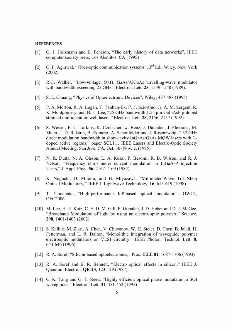
Fig. 2.1 CPW geometry and corresponding electric and magnetic field distribution [1]......................................................................................................................................21
Fig. 2.2 CPS geometry and corresponding electric and magnetic field distribution [1]......................................................................................................................................22
Fig. 2.3 Asymmetric CPS ............................................................................................22
Fig. 2.4 Calculated characteristic impedance as function of different geometry parameters of CPS using semi-isolating InP as substrate ............................................24
Fig. 2.5 Voltage and current definitions and equivalent circuit for an incremental length of transmission line ...........................................................................................26
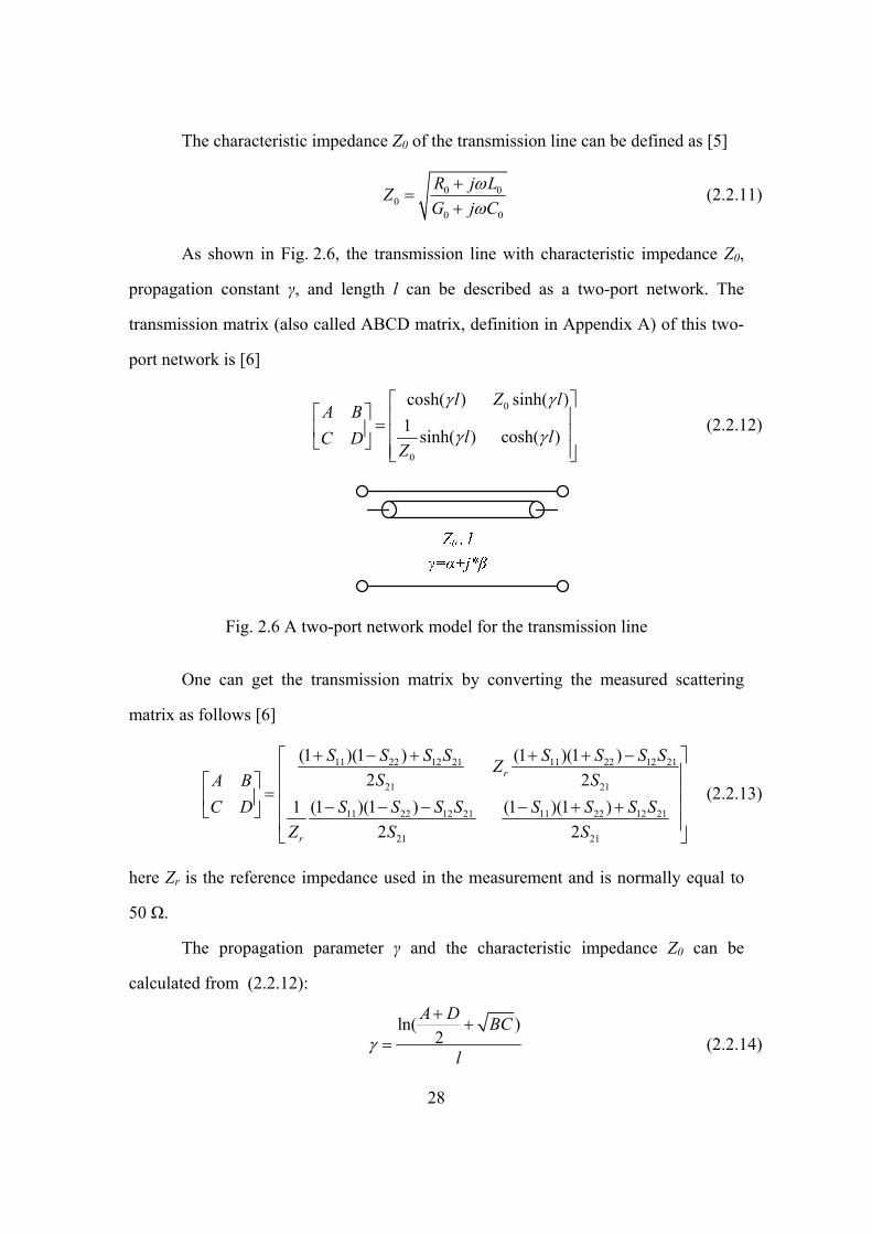
Fig. 2.6 A two-port network model for the transmission line......................................28
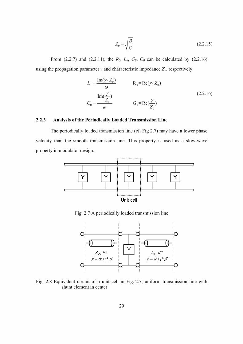
Fig. 2.7 A periodically loaded transmission line .........................................................29
Fig. 2.8 Equivalent circuit of a unit cell in Fig. 2.7, uniform transmission line with shunt element in center ................................................................................................29
Fig. 2.9 Lattice constant and bandgap energies of ternary and quaternary compounds formed by using III-V group semiconductors [10] ......................................................32
Fig. 2.10 p-n junction under (a) reverse and (b) forward bias .....................................34
Fig. 2.11 Distributed resistance model of a contact to a thin semiconductor layer .....39
Fig. 2.12 (a) A TLM test structure and (b) contact resistance versus contact spacing......................................................................................................................................40
Fig. 2.13 Illustration of index ellipsoid, the dashed ellipse is the intersection of the index ellipsoid with the plane normal to the propagation direction.............................41
Fig. 2.14 Energy levels of a QW structure without and with applied electric field [16]......................................................................................................................................44
Fig. 2.15 Simulated absorption spectra for a QW under different electric field [15] ..46
xi
Fig. 3.1 Schematic of a Mach-Zehnder Interferometer with 2 Y-branch ....................49
Fig. 3.2 Transfer curve for MZI with 2 Y-branches ....................................................50
Fig. 3.3 Transfer curve of an MZI with 2 Y-branches with optical loss, b=0.9 ..........51
Fig. 3.4 Schematic of a MZM with a lumped electrode ..............................................52
Fig. 3.5 Cross section of the optical waveguide covered with a lumped electrode .....52
Fig. 3.6 The equivalent circuit model for the MZM with a lumped electrode ............52
Fig. 3.7 Schematic of a MZM with push-pull lumped electrodes ...............................54
Fig. 3.8 The circuit model for series push-pull [4] ......................................................54
Fig. 3.9 Schematic of a MZI with one Y-branch and a 2×2 MMI and the ideal transfer matrix for each section.................................................................................................54
Fig. 3.10 Transmission character of Mach-Zehnder interferometer ............................56
Fig. 3.11 Intensity modulation using push-pull structure ............................................56
Fig. 3.12 Schematic of a MZM with capacitive loaded segmented traveling-wave electrode.......................................................................................................................58
Fig. 3.13 Cross sectional view of a MZM with DC bias and HF circuit diagram .......58
Fig. 3.14 Microwave design of the capacitively loaded TWE MZM ..........................60
Fig. 3.15 Equivalent circuit of a traveling-wave electrode modulator ........................61
Fig. 4.1 Flow chart of general design process of HFSS...............................................72
Fig. 4.2 Flow chart of the HFSS adaptive refinement process ....................................73
Fig. 4.3 Simplified p-layer in modulator modeling in HFSS.......................................76
Fig. 4.4 Carrier concentration of different layers in modulator with varied bias [7]...77
Fig. 4.5 Top-view of a whole chip modulator model with 12 sections in HFSS.........78
Fig. 4.6 (a) A section of modulator (b) An N-section segmented modulator ...........78
Fig. 4.7 An 8-cell 2-port network in Ansoft Designer .................................................79
Fig. 4.8 (a) Top-view (b) Side-view of a single-section modulator model in HFSS...80
Fig. 4.9 A 3-D view of a single-section modulator model with excitation and boundary condition ......................................................................................................80
Fig. 4.10 Comparison between measured and simulated electrical insertion loss S21 of the same modulator structure .......................................................................................81
Fig. 4.11 Microwave equivalent model for the TWE MZM........................................82
Fig. 4.12 One cell of the modulator and its transmission matrix.................................83
xii
Fig. 4.13 Transmission matrix representation of TWE MZM .....................................84
Fig. 4.14 Calculated L0 and C0 for an unloaded CPS...................................................85
Fig. 4.15 Measured bias dependent capacitance of circular p-i-n diodes ....................86
Fig. 4.16 SEM photo of inner electrodes of the modulator .........................................87
Fig. 4.17 Parasitic capacitance in the active area of a modulator ................................88
Fig. 4.18 The resistances in the active area of a modulator .........................................89
Fig. 4.19 The hierarchical model for one section of a modulator in an EDA tool ......90
Fig. 4.20 Circuit models of passive part and active part in a section of the modulator......................................................................................................................................90
Fig. 4.21 12-section TWE MZM model in ADS .........................................................91
Fig. 4.22 The simulation results using the detailed model ..........................................92
Fig. 4.23 Measured S21 parameters of two modulators (l=3 mm, η=0.4) with 250 μm and 500 μm period length, respectively .......................................................................93
Fig. 4.24 The propagation of optical and electrical signals in the modulator [14] ......95
Fig. 4.25 Measured data of a 12.2 mm long waveguide by the Fabry-Perot method ..97
Fig. 4.26 Measured S11 and converted corresponding nμ of a modulator (#45C63) ....98
Fig. 4.27 Measured phase and converted corresponding nμ of a modulator (#45C63) 99
Fig. 4.28 Microwave index and the optic index of two modulators ..........................100
Fig. 4.29 Cross-sectional view of CPS test structures ...............................................101
Fig. 4.30 Microwave indices of unloaded TWE test structures.................................101
Fig. 4.31 Electro-optical response of the modulators with and without BCB layer ..102
Fig. 4.32 The electro-optical responses of a modulation under co- and counter- propagation conditions, respectively .........................................................................103
Fig. 4.33 The CPS structures simulated in HFSS ......................................................105
Fig. 4.34 Simulated insertion loss of 1 mm CPS .......................................................105
Fig. 4.35 CPS with mesa............................................................................................106
Fig. 4.36 The impact of mesa width on the insertion loss of the CPS .......................107
Fig. 4.37 The impact of the series resistance in the active area on the insertion loss of the modulator ( for Rc=10.7 Ω, the corresponding ρc is 3×10⁻⁵ cm2·Ω )....................108
Fig. 4.38 Simulated insertion loss of modulators with different ρc using HFSS .......110
Fig. 4.39 Simulation results of optimized modulator with different fill factors ........112
xiii
Fig. 4.40 The relationship between the 3 dBeo bandwidth, the driving voltage and the fill factor of a modulator ............................................................................................114
Fig. 4.41 Measured C-V curves with two different i-region thickness......................115
Fig. 4.42 The measured Vπ before and after optimizing i-layer’s thickness..............116
Fig. 4.43 Loading capacitance as function of microwave index of the unloaded CPS....................................................................................................................................116
Fig. 4.44 Cross sectional view of the modulator (a) before and (b) after redesign ...117
Fig. 4.45 Characteristic impedance for CPS as a function of aspect ratio a/b ...........118
Fig. 4.46 Flow chart of the redesign process .............................................................119
Fig. 5.1 SEM photo of a pair of air bridges between TWE and optical waveguide in a fabricated modulator ..................................................................................................124
Fig. 5.2 SEM photo of one side of a fabricated modulator........................................124
Fig. 5.3 (a) A 3-D model of the spot size converter with field distribution for the fundamental mode in the passive and fiber port waveguide, respectively (b) Alignment tolerances measured at the input port of the modulator compared to that of the tolerances of a tapered fiber to a passive waveguide [1] .....................................125
Fig. 5.4 The CAD drawing of a packaged modulator module...................................126
Fig. 5.5 Measured electrical loss S21 of a modulator before and after packaging .....127
Fig. 5.6 A simplified 3-D model in HFSS .................................................................128
Fig. 5.7 Top-view and side-view of the 3-D model of a packaged module and simulation results .......................................................................................................129
Fig. 5.8 Bonding wires (a) two bonding wires for each connection, (b) five bonding wires for ground and three for signal .........................................................................130
Fig. 5.9 An optimized integrated CPS-CPW transition in a modulator.....................131
Fig. 5.10 Three different configurations of input and output pads (a) asymmetrical S-G configuration, (b) symmetric S-G configuration, (c) G-S-G pads, (d) measured electrical insertion losses of the three different configurations .................................131
Fig. 5.11 The module using G-S-G pads with long ground bar on the middle block 132
Fig. 5.12 The module using G-S-G pads with separated middle blocks....................133
Fig. 5.13 Simulated electrical insertion loss S21 of a modulator before and after optimized packaging ..................................................................................................133
Fig. 6.1 The circular diode test structure: top view and cross sectional view. ..........134
Fig. 6.2 Measured C-V characteristic of round diodes ..............................................135
xiv
Fig. 6.3 Intrinsic layer thickness over bias voltage deduced from C-V measurements....................................................................................................................................135
Fig. 6.4 Layout of one TLM structure (wc=100 μm) .................................................136
Fig. 6.5 Measured p-contact resistivities of two modulator wafers ...........................137
Fig. 6.6 Setup of DC matrix measurement [2]...........................................................139
Fig. 6.7 (a) Normalized optical transmission with applied voltage to I- and U-electrode. (b) The transfer curve of the corresponding operating point in (a) ........140
Fig. 6.8 The setup of electrooptic response measurement (200 MHz – 65 GHz) [3] 143
Fig. 6.9 Setup for 40 Gbit/s eye-diagram measurements of modulator .....................145
Fig. 6.10 Setup for 80 Gbit/s eye-diagram measurements of modulator ...................146
Fig. 7.1 A packaged modulator module [1] ...............................................................149
Fig. 7.2 Normalized output vs. driving voltage of the module (#45 A50) at -2.8 V bias....................................................................................................................................149
Fig. 7.3 EO response of the packaged MZI modulator (#45 A50) at -2.8 V bias [1] 150
Fig. 7.4 Measured NRZ eye diagram of the packaged MZI modulator (#45 A50) at 40 Gbit/s with 1.55 µm optical signal (PRBS word length: 231-1, 10 ps/div) [1]......150
Fig. 7.5 Measured 40 Gbit/s PRBS BER curves of the packaged modulator (#45A50)....................................................................................................................................151
Fig. 7.6 Measured NRZ eye diagram of the packaged MZI modulator (#45 A50) at 80 Gbit/s with 1.55 µm optical signal (PRBS word length: 215-1, 5ps/div) ..............152
Fig. 7.7 Electro-optical response of a modulator (on-chip) with a TWE length of 4 mm. (lE= 200 µm, Λ= 500 µm, -6 V bias)...............................................................153
Fig. A.1 An arbitrary N-port network [1] ..................................................................155
Fig. A.2 A two-port network......................................................................................156
Fig. A.3 A cascade connection of two two-port networks.........................................156

xv
List of Symbols
α Microwave attenuation constant
αc attenuation constant due to Ohmic loss
αchirp chirp parameter
αd attenuation constant due to dielectric loss
βμ complex microwave propagation constant of the signal
in the electrode
βopt complex optical propagation constant of the signal in the
optical waveguide μβopt velocity mismatch in the modulator
γ complex transmission constant
δ skin effect factor
εreff effective dielectric constant
η fill factor of a modulator
λ wavelength
λ0 wavelength in free space
Λ period length of a modulator
μe electron mobility
μh hole mobility
ρ1 input electrode structure reflection coefficient
ρ2 output electrode structure reflection coefficient
ρc contact resistivity
σ conductivity
ωm modulation frequency
φ(f) accumulated phase delay of S21
a lattice constant
b optical imbalance factor in MZI
C0 shunt capacitance per unit length

xvi
CL loading capacitance of a modulator per unit length
Cpin junction capacitance of the p-i-n diode per unit area
Cs parasitic capacitance per unit length
d distance between two optical waveguides
db diameter of the air-bridge
di thickness of intrinsic layer
dp thickness of the p-layer
dpin depletion layer width of reverse biased pin diode
ds skin depth
Eg bandgap energy
fBragg Bragg frequency
G0 shunt conductance per unit length
l traveling-wave electrode length
L0 series inductance per unit length
Lb inductance of the air-bridge
lb length of the air-bridge
lE active electrode length
leff effective modulation length
n electron density
n0 optical index of the active layer at zero applied voltage
nopt optical index
nμ microwave index
nμ’ microwave index of the loaded CPS
p hole density
Pin input optical power
Pout output optical power
r modulation reduction factor
R0 series resistance per unit length
Rc contact resistance
rij electro-optic coefficient
Rn bulk resistance of the n-layer

xvii
Rp bulk resistance of the p-layer
Rsh sheet resistance
tanδ dielectric loss tangent
TMZI optical intensity transfer function
vµ velocity of the electrical signal
Vg amplitude of the generator voltage
vgr-o group velocity of the optical signal
vopt velocity of the optical signal
vp phase velocity
Vπ driving voltage
wc width of the contact
wwg width of the optical waveguide
Z0 characteristic impedance of unloaded CPS
Zm characteristic impedance of the modulator
ZS source impedance, normally is 50 Ω
ZT terminating impedance
Δλ wavelength difference between two adjacent maximum
points
Δφ phase difference
xviii
List of Abbreviations
3-D Three dimensional
ASE Amplified spontaneous emission
BCB Benzocyclobuten
BER Bit error rate
CPS Coplanar strips
CPW Coplanar waveguides
C-V Capacitance-Voltage
CW Continuous wave
DWDM Dense wavelength division multiplexing
EA Electroabsorption
EAM Electroabsorption modulator
ECL External cavity laser
EDFA Erbium-doped fiber amplifier
EM Electromagnetic
EO Electro-optic
ETDM Electrical time division multiplexing
FEM Finite element method
GPIB General purpose interface bus
G-S Ground signal
G-S-G Ground signal ground
III-V Semiconductor based on group III and group V elements
MBE Molecular beam epitaxy
MMI Multimode interference
MOCVD Metal organic chemical vapor deposition
MQW Multi quantum wells
MZI Mach-Zehnder interferometer
MZM Mach-Zehnder modulator
NLO Nonlinear optical
NRZ Non return to zero

xix
PRBS Pseudorandom binary sequence
QCSE Quantum confined Stark effect
SEM Scanning electron microscope
S-G Signal ground
SOA Semiconductor optical amplifier
SOLT Short, open, load, thru
SSC Spot-size converter
TDM Time division multiplexing
TE Transverse electric
TEM Transverse electromagnetic
TLM Transmission line method
TM Transverse magnetic
TWE Traveling-wave electrode
WDM Wavelength division multiplexing

xx
1
Chapter 1
Introduction
1.1 OVERVIEW
The use of light for communication purposes is not new. It can date back to
antiquity if we interpret optical communications in a broad sense [1]. Most
civilizations have used mirrors, fire beacons, or smoke signals to convey a single
piece of information [2].
Development of fibers and devices for optical communication began in the
early 1960s and continues strongly today. But the real change came in the 1980s.
During this decade optical communication in public communication networks
developed from the status of a curiosity into being the dominant technology.
Transmitting signals by using light through optical fiber is the most effective way to
move large amounts of data rapidly over long distances. Nowadays, in the era of
information technology, the optical fiber transmission links form the backbone of the
communications infrastructure. Recently, the bit rates of the electrical time-domain
multiplexed (ETDM) system are improving from 2.5 Gbit/s to 10 Gbit/s and even
40 Gbit/s in deployed systems.
It is well known that the electrical signal still conquers our communication
terminals in everyday life. But to take advantage of the optical transmission system,
these electrical signals must be converted into optical ones which can be transferred in
fibers. The electro-optic modulator (cf. Fig. 1.1) is such a device that converts the
electrical signal to the optical one. For example, in a 40 Gbit/s electrical time-division
multiplexing (ETDM) transmitter, low speed signals used in communication terminals
will be hierarchically multiplexed into a high speed one (40 Gbit/s) at first, and then
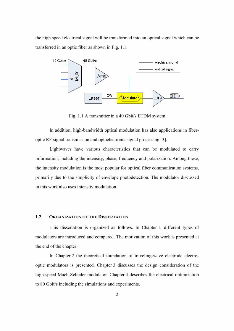
2
the high speed electrical signal will be transformed into an optical signal which can be
transferred in an optic fiber as shown in Fig. 1.1.
Fig. 1.1 A transmitter in a 40 Gbit/s ETDM system
In addition, high-bandwidth optical modulation has also applications in fiber-
optic RF signal transmission and optoelectronic signal processing [3].
Lightwaves have various characteristics that can be modulated to carry
information, including the intensity, phase, frequency and polarization. Among these,
the intensity modulation is the most popular for optical fiber communication systems,
primarily due to the simplicity of envelope photodetection. The modulator discussed
in this work also uses intensity modulation.
1.2 ORGANIZATION OF THE DISSERTATION
This dissertation is organized as follows. In Chapter 1, different types of
modulators are introduced and compared. The motivation of this work is presented at
the end of the chapter.
In Chapter 2 the theoretical foundation of traveling-wave electrode electro-
optic modulators is presented. Chapter 3 discusses the design consideration of the
high-speed Mach-Zehnder modulator. Chapter 4 describes the electrical optimization
to 80 Gbit/s including the simulations and experiments.
3
Chapter 5 explains the fabrication process and the involved packaging
technology.
Chapter 6 introduces the corresponding measurements that are used for
characterizing the modulators and test structures.
Chapter 7 shows experimental results and gives an overall summary and an
outlook of further work.
1.3 DIRECT MODULATION
There are two groups of modulation methods: one is direct modulation, the
other is external modulation. Each has its own pros and cons. They will be introduced
in this and next section in detail.
The most straightforward method for modulation is to directly modulate the
laser source. Due to the requirements of bandwidth and efficiency, only
semiconductor lasers are of practical interest for direct modulation [4].
A unique feature of semiconductor lasers is that the semiconductor laser can
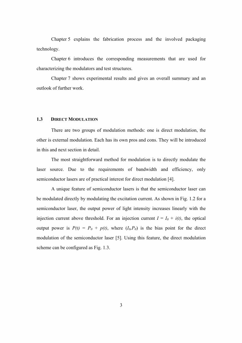
be modulated directly by modulating the excitation current. As shown in Fig. 1.2 for a
semiconductor laser, the output power of light intensity increases linearly with the
injection current above threshold. For an injection current I = I0 + i(t), the optical
output power is P(t) = P0 + p(t), where (I0,P0) is the bias point for the direct
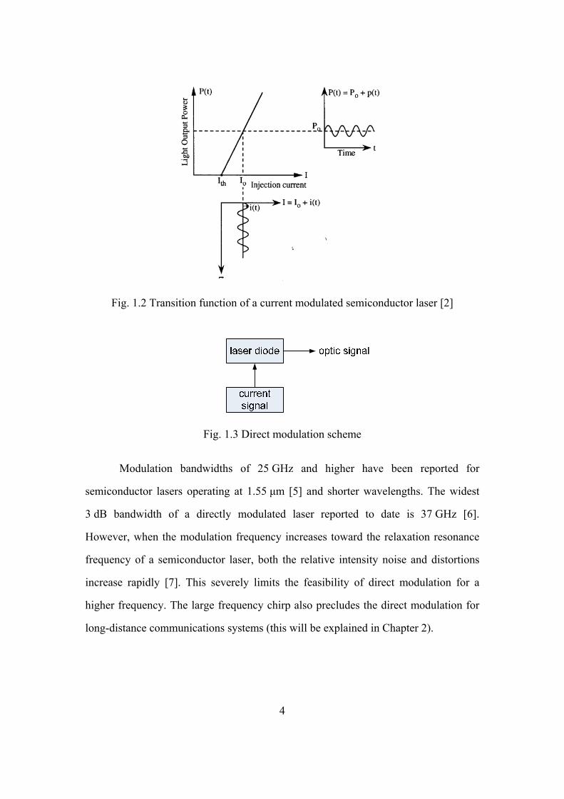
modulation of the semiconductor laser [5]. Using this feature, the direct modulation
scheme can be configured as Fig. 1.3.
4
Fig. 1.2 Transition function of a current modulated semiconductor laser [2]
Fig. 1.3 Direct modulation scheme
Modulation bandwidths of 25 GHz and higher have been reported for
semiconductor lasers operating at 1.55 μm [5] and shorter wavelengths. The widest
3 dB bandwidth of a directly modulated laser reported to date is 37 GHz [6].
However, when the modulation frequency increases toward the relaxation resonance
frequency of a semiconductor laser, both the relative intensity noise and distortions
increase rapidly [7]. This severely limits the feasibility of direct modulation for a
higher frequency. The large frequency chirp also precludes the direct modulation for
long-distance communications systems (this will be explained in Chapter 2).
5
1.4 EXTERNAL MODULATORS
At bit rates of 10 Gbit/s or higher, the frequency chirp imposed by direct
modulation becomes large enough that direct modulation of semiconductor laser is
rarely used [2].
Unlike direct modulation, external modulation has been shown to have
superior performance for wide bandwidth optical fiber communications, however with
the potential disadvantages of adding system complexity and cost.
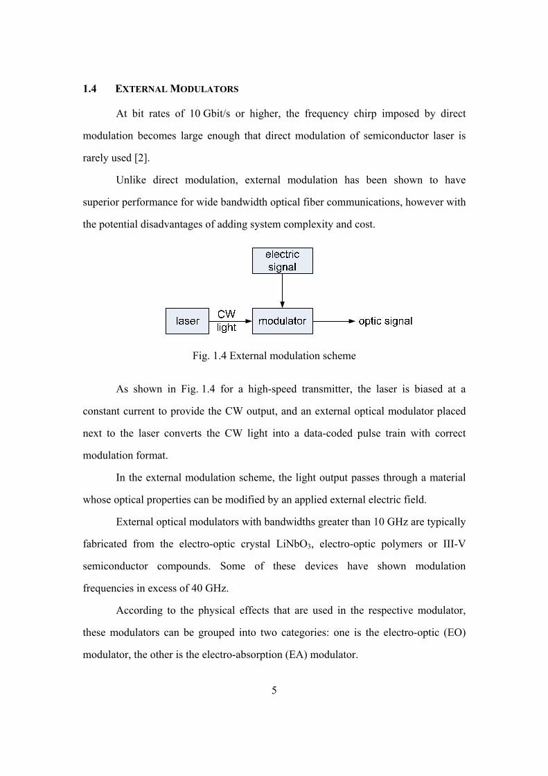
Fig. 1.4 External modulation scheme
As shown in Fig. 1.4 for a high-speed transmitter, the laser is biased at a
constant current to provide the CW output, and an external optical modulator placed
next to the laser converts the CW light into a data-coded pulse train with correct
modulation format.
In the external modulation scheme, the light output passes through a material
whose optical properties can be modified by an applied external electric field.
External optical modulators with bandwidths greater than 10 GHz are typically
fabricated from the electro-optic crystal LiNbO3, electro-optic polymers or III-V
semiconductor compounds. Some of these devices have shown modulation
frequencies in excess of 40 GHz.
According to the physical effects that are used in the respective modulator,
these modulators can be grouped into two categories: one is the electro-optic (EO)
modulator, the other is the electro-absorption (EA) modulator.
6
1.4.1 Electro-Optic Modulators
The electro-optic effect is most widely used for high speed modulation.
Electro-optic modulators can produce amplitude, frequency or phase modulation in an
optical signal by exploiting the electro-optic effect in which the optical properties of a
crystal can be altered by an electric field.
Directional coupler and Mach-Zehnder interferometer are two waveguide
structures that are often used for intensity modulation with the electro-optic effect.
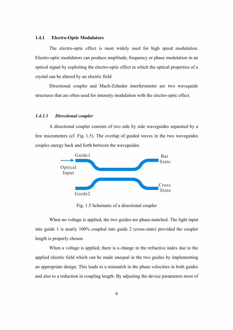
1.4.1.1 Directional coupler
A directional coupler consists of two side by side waveguides separated by a
few micrometers (cf. Fig. 1.5). The overlap of guided waves in the two waveguides
couples energy back and forth between the waveguides.
Optical Input
Guide1
Guide2
BarState
Cross State
Fig. 1.5 Schematic of a directional coupler
When no voltage is applied, the two guides are phase-matched. The light input
into guide 1 is nearly 100% coupled into guide 2 (cross-state) provided the coupler
length is properly chosen.
When a voltage is applied, there is a change in the refractive index due to the
applied electric field which can be made unequal in the two guides by implementing
an appropriate design. This leads to a mismatch in the phase velocities in both guides
and also to a reduction in coupling length. By adjusting the device parameters most of
7
the power can be transferred back to guide 1 (the bar-state) at the end of the
directional coupler.
For directional coupler devices based on bulk material, the size of the device is
fairly large since the electro-optic coefficient is not so large. Typically, the devices
require an interaction length of ~1cm or more and a bias voltage of ~5-10V. The
switching voltage of a directional coupler modulator is 3 times larger than that
required for a Mach-Zehnder modulator (see section 1.4.1.2). Due to these reasons,
for digital applications the directional coupler structure is less been used than the
Mach-Zehnder interferometer in intensity modulator design.
However, recent research shows that with multi-section design directional
coupler based modulators have high linearity which is important for analog
applications, such as RF-fiber links. Several corresponding designs have been
published [12,13].
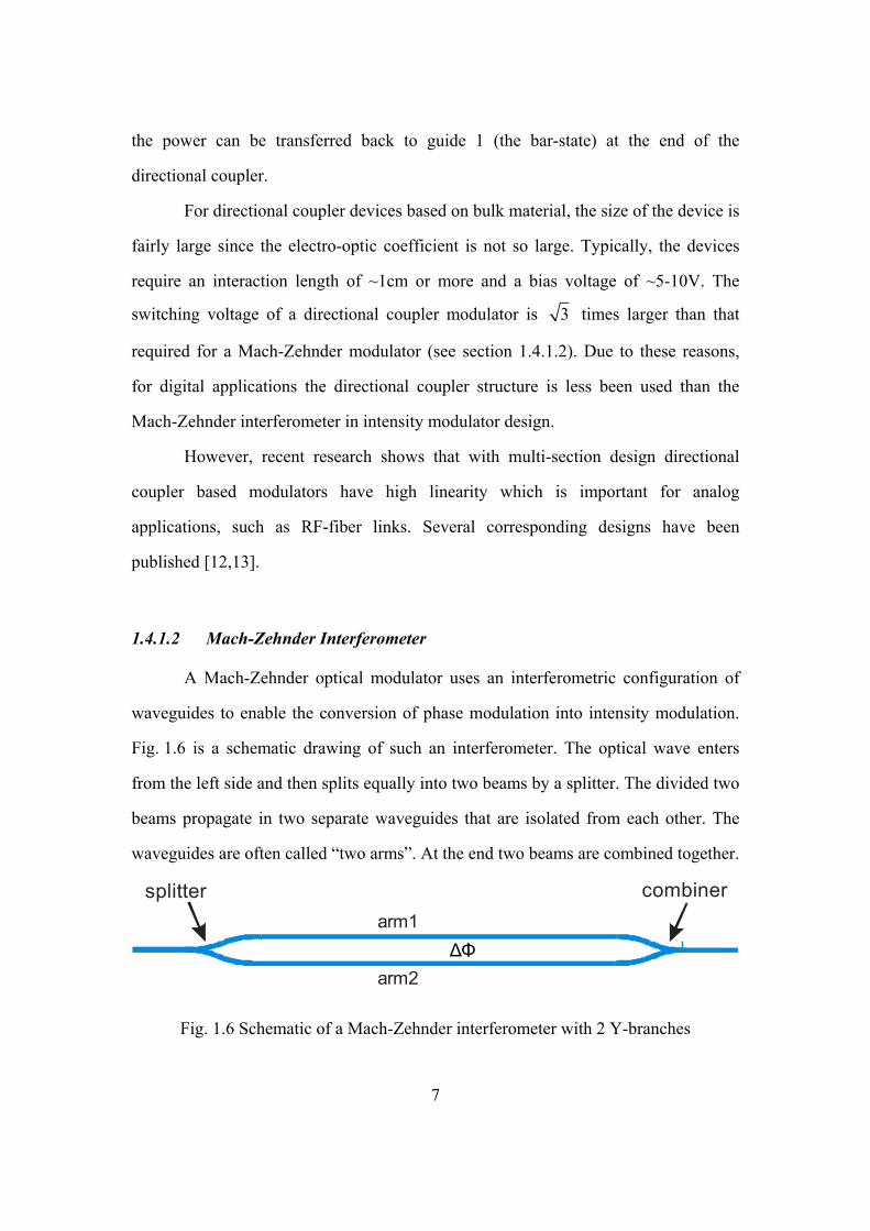
1.4.1.2 Mach-Zehnder Interferometer
A Mach-Zehnder optical modulator uses an interferometric configuration of
waveguides to enable the conversion of phase modulation into intensity modulation.
Fig. 1.6 is a schematic drawing of such an interferometer. The optical wave enters
from the left side and then splits equally into two beams by a splitter. The divided two
beams propagate in two separate waveguides that are isolated from each other. The
waveguides are often called “two arms”. At the end two beams are combined together.
arm1
arm2
combinersplitter
ΔΦ
Fig. 1.6 Schematic of a Mach-Zehnder interferometer with 2 Y-branches
8
The splitter and combiner here can be a Y-branch, a directional coupler or a
2×2 multimode interference (MMI) coupler.
A relative phase difference Δφ is introduced between two arms. When the
differential phase shift Δφ between the two arms equals π± , destructive interference
occurs, corresponding to the off-state or “0” level for the modulator. With no
differential phase shift, constructive interference occurs, corresponding to the on-state
or “1” level for the modulator.
Due to its simple structure and the potential of push-pull operation (further
discussed in Chapter 3), the Mach-Zehnder interferometer (MZI) is the most popular
device for implementing optical intensity modulation using the electro-optic effect.
The modulators in this work are also based on the concept of the MZI.
1.4.1.3 Materials
Many different materials can be used to fabricate electro-optic modulators,
including lithium niobate, III-V compounds, polymers and even silicon. In this
section, a brief introduction will be given for each material mentioned above.
Lithium Niobate (LiNbO3)
Lithium niobate (LiNbO3) is the most widely used material for the
manufacture of electro-optic devices, including phase modulators, polarization
modulators, Mach-Zehnder intensity modulators and directional-coupler intensity
modulators.
LiNbO3 is a ferroelectric anistropic crystal with 3-m crystal symmetry.
Depending on the orientation of an applied electric field, different electrooptic
coefficients are relevant.
The most popular method of fabricating optical waveguides in LiNbO3 is
accomplished by diffusing titanium (Ti) which is deposited at the desired location of
9
the waveguide [8]. The dimensions of the optical waveguide can be controlled by
properly choosing the initial Ti stripe width, film thickness and diffusion conditions.
The resulting single-mode waveguide has a very low optical propagation loss,
typically less than 0.2 dB/cm, and its mode size can be matched very well to that of a
single-mode optical fiber.
Due to its properties of enabling low-loss waveguides, high electro-optic effect
and high optical coupling efficiency with single-mode optical fiber, so far LiNbO3 has
been the material of choice for optical modulators at bit rates of 10 Gbit/s and above.
LiNbO3 travelling-wave modulators, based on a Mach-Zehnder interferometer
waveguide structure, are the most widespread modulators in deployed systems [8].
However, LiNbO3 Mach-Zehnder modulators have not only a large size, but
also a bias-drifting problem which requires an extra bias control circuit. High driving
voltage also limits their applications. In addition, the LiNbO3 modulator is difficult to
be integrated with other components
III-V Semiconductors
III-V compound semiconductors, such as GaAs, InP and their ternary and
quaternary alloys, are also candidate materials for EO modulators. There are two
types of applications: one is using bulk material, the other is based on multi-quantum-
wells (MQW).
Although their EO coefficients (defined in section 2.6) are 20 times smaller
than that of LiNbO3, efficient modulation can still be obtained with these materials.
This is because semiconductor crystal growth and fabrication techniques provide great
flexibility for waveguide geometry control, so that the optical guided mode can be
confined to a very small region (2-3 μm spot size), and thus a very large electric field
can be achieved even with a small voltage applied across the small dielectric gap.
Additionally, III-V semiconductors have large optical refractive indices, for example,
at optical wavelength of 1.3-1.6 μm, the optical index is 3.2 for InP and 3.4 for GaAs,
10
compared to 2.2 for LiNbO3. This indicates a 3-4 times improvement for the index
change in a linear electro-optic modulation application. All these factors make the
efficiency of III-V EO modulators comparable to that of LiNbO3 modulators. In
addition, III-V EO modulators can potentially be integrated with a wide range of
components such as lasers, semiconductor optical amplifiers (SOAs), photodetectors,
passive optical circuits and even electronic drivers.
One popular type of III-V semiconductor EO modulator is based on bulk
GaAs/AlGaAs waveguides grown on GaAs substrates due to the availability of large
GaAs substrates (4" diameter), and those EO modulators are typically 2-3 cm long. In
the GaAs/AlGaAs waveguide, the GaAs layer has higher optical index than the
AlGaAs layer, the latter is lattice-matched to GaAs for all values. By sandwiching the
GaAs layer between two AlGaAs layers, optical confinement in the vertical growth
direction can be achieved. The lateral optical confinement is usually obtained by
material etching. Shallow-etched rib waveguides are preferred over deep-ridge
waveguides to achieve single-mode waveguiding. The resulting optical waveguides
may have propagation loss ranging from tenths of dB/cm to a few dB/cm, depending
on the waveguide structure and the fabrication process.
Another type of modulator, which is also made of III-V compound materials,
uses the quantum confined Stark effect (QCSE) in multi-quantum-wells (MQW).
Since strong index changes can be induced by QCSE (this will be discussed in detail
in section 2.7), the relevant driving voltage for this type of device is relatively low
compared to that of LiNbO3 modulators. This is very attractive, because the lower the
driving voltage is, the lower the power consumption, cost and size of the transmitter
module become [9]. In addition, the compact size is also a notable advantage. The
modulators in this work are also of this type.
11
Polymers
Compared to LiNbO3 and III-V semiconductors, organic polymers are
relatively immature EO materials, but they also possess a great potential for more
advanced modulators. For example, a polymer modulator operating up to 150 GHz
was reported in 2002 [10].
The advantages of EO polymers mostly come from the applicability of the
spin-coating technique. This does not only make it possible to integrate polymer EO
devices with various electronic and optoelectronic components [11], but also offers
the opportunity to fabricate multiple devices stacked in the vertical direction. Metal
electrodes can be buried between different polymer layers, and this makes the
electrode design very flexible. To lower the fabrication cost, polymer EO devices can
be fabricated directly on top of optical submounts. The optical refractive index of
polymers is close to that of single-mode optical fibers. This provides a good match
between the polymer waveguide mode and the fiber mode.
Polymer modulators may have great potential in the future, but their optical
power handling capability is currently much less than that of modulators based of
other materials, and their thermal and photochemical stabilities need to be improved.
Silicon
Unlike the materials mentioned before, silicon as a ‘new’ material of optical
components has been prompted on account of the demand for low-cost solutions from
industry. There are also strong motivations for considering optics for shorter distance
interconnects, especially using silicon photonic, a platform in which one could make
electronics, waveguides, other optical components and optoelectronic devices.
Silicon is attractive from a cost standpoint because mature silicon processing
technology and manufacturing infrastructure already exist and can be used to build
cost-effective devices in large volume. In addition, silicon photonics technology
12
provides the possibility of monolithically integrating optical elements and advanced
electronics on silicon using bipolar or CMOS technology [12].
Although unstrained pure crystalline silicon exhibits no linear electro-optic
effect and the refractive index changes due to the Franz-Keldysh and Kerr effects are
also small [13], several silicon waveguide-based optical modulators have been
proposed and demonstrated [14,15] by using the free carrier plasma dispersion effect
in a forward-biased pin diode geometry.
Since the modulation speed due to the free carrier plasma dispersion effect is
determined by the rate at which carriers can be injected and removed, the long
recombination carrier lifetime in the intrinsic silicon region generally limits the
modulation frequency of these silicon-based devices.
A breakthrough was claimed by a group from Intel Corp. in 2004. They made
a Si-based electro-optical modulator that can modulate light at 1~2 GHz, which is
unprecedented in a silicon-based modulator, by introducing a metal-oxide-
semiconductor (MOS) capacitor as phase shifter into the modulator structure [16].
Because charge transport in the MOS capacitor is governed by majority carriers, the
device bandwidth is not limited by the relatively slow carrier recombination processes
of pin diode devices. This group had optimized the device for a 10 Gbit/s application,
recently [17].
Another breakthrough in silicon modulators was announced in 2005 by a team
from Stanford University. They have reported that QCSE in thin germanium
quantum-well structures grown on silicon has strengths comparable to that in III-V
materials [18]. This discovery may be promising for small, high-speed, modulator
devices fully compatible with silicon electronics manufacture.
Although there have been claimed breakthroughs in silicon-based modulator
design, currently the modulation bandwidth and the power consumption of such
devices is still not comparable with that of modulators based of other materials.
13
1.4.2 Electroabsorption Modulators
The electroabsorption (EA) effect denotes the change of the optical absorption
coefficient in materials due to the presence of an electric field. The EA effect in a
single optical waveguide directly results in optical intensity modulation. The primary
materials for fabricating EAMs working at 1.3-1.6 μm optical wavelengths are
currently III-V semiconductors, specifically, ternary and quaternary alloys (including
InGaAs, InAlAs, InAsP, InGaP, InGaAsP and InGaAlAs, etc.) grown on InP
substrate. Similar to semiconductor-based EO modulators, EAMs can also be
integrated with a variety of other devices. The most notable integrated chips include
electroabsorption modulated lasers (EML) [19], and tandem EA modulators (often
with SOA) for RZ data transmission and wavelength-division demultiplexing [20].
Another attraction of EAMs is their compact size (typically 80-300 μm long) due to
their high efficiency. This leads to small footprint for a single device and high yield
per wafer which lowers the fabrication cost.
An EA waveguide usually consists of p-i-n semiconductor layers, among
which the intrinsic layer has higher optical refractive index than the p-type and n-type
doped layers. This provides vertical optical confinement. The lateral optical
confinement is usually achieved by a deep mesa etch. The etched deep-ridge
waveguide can then be planarized using polyimide or regrown semi-insulating InP. In
a typical EA waveguide design, both the optical mode and the applied electric field
are tightly confined in a small area around the intrinsic layer, which enables highly
efficient modulation.
The optical propagation loss in EA waveguides is much larger than that in EO
waveguides, typically ranging from 15 to 20 dB/mm. This high optical propagation
loss is mainly attributed to three sources: the first is the residual absorption loss in the
active layer; the second is the interband absorption loss induced by free carriers in the
highly doped layers, primarily in p-type layers; the third is the scattering loss caused
14
by the roughness of the deep-ridge waveguide sidewalls and defects in the grown
materials. Fortunately, due to their short length the overall optical loss is tolerable.
The tight optical confinement results in a small, elliptical mode profile in EA
waveguides, typically 2-4 μm lateral and 1-2 μm vertical effective mode sizes which
can have large optical coupling loss to a single-mode optical fiber whose mode size is
typically 9 μm in diameter. To overcome this problem, either a micro ball lens is
inserted between the EA waveguide and the fiber tip, or an optical lens can be directly
fabricated on the fiber tip to produce a mode size of 3-4 μm at the focal plane that is
20 μm away from the fiber tip. Integrating a spot-size converter (SSC) at both ends of
the EA waveguide can further reduce the coupling loss. A SSC is a passive optical
waveguide with adiabatic vertical and/or lateral tapers in geometry and/or optical
refractive index. It converts the small elliptical EA waveguide mode at one end to a
near-circular expanded mode (mode size 3-4 μm) at the other end, or vice versa.
Integrating with a SSC makes the EAM longer, which makes cleaving and handling
easier and also reduces the amount of unguided light directly coupled from the input
fiber to the output fiber, resulting in an improved ON/OFF extinction ratio for digital
links. Such SSC can be also used in a MQW based EO modulator.
Compared with EO modulators, the main disadvantages of EAM are low
saturation power, large chirp, narrow optical bandwidth and need of temperature
control. Nevertheless, EAMs are very attractive due to their small chip-size, low
driving voltage and the compatibility for integration with other components. Limited
by their inherent chirp, EAMs are not suitable for long-haul systems and are normally
used in short distance transmission systems.
15
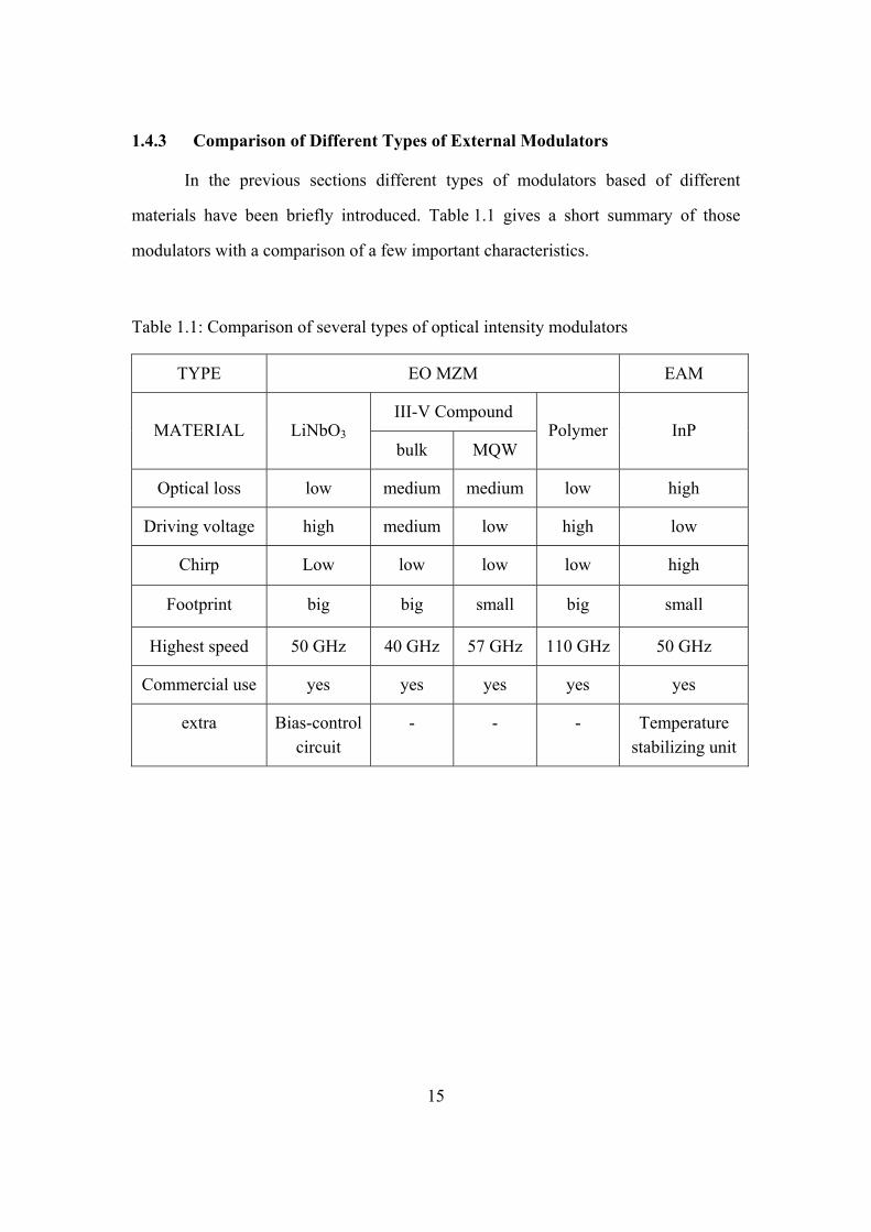
1.4.3 Comparison of Different Types of External Modulators
In the previous sections different types of modulators based of different
materials have been briefly introduced. Table 1.1 gives a short summary of those
modulators with a comparison of a few important characteristics.
Table 1.1: Comparison of several types of optical intensity modulators
TYPE EO MZM EAM
III-V Compound MATERIAL LiNbO3
bulk MQW Polymer InP
Optical loss low medium medium low high
Driving voltage high medium low high low
Chirp Low low low low high
Footprint big big small big small
Highest speed 50 GHz 40 GHz 57 GHz 110 GHz 50 GHz
Commercial use yes yes yes yes yes
extra Bias-control circuit
- - - Temperature stabilizing unit
16
1.5 MOTIVATION FOR THE WORK
The rapid growth of data traffic, caused mainly by increasing use of the
Internet including recent expanded use of multimedia services and wireless access,
has stimulated the demand for high-capacity photonic network systems. High capacity
optical networks are based on a combination of wavelength-division multiplexing
(WDM) and time-division multiplexing (TDM) for purposes ranging from long-
distance transmission between nodes to short-reach optical links such as metro/access
links. Moreover, the next generation networks (NGN) are not far away from us and
the 100 Gbit/s Ethernet is also in progress. All of these will inevitably need
transmitters which can operate above 40 Gbit/s.
The maximum direct modulation bandwidth in semiconductor lasers in limited
to a few GHz. The frequency chirp associated with high-speed direct modulation of
laser diodes above a few Gbit/s has become a clear problem and results in serious
consequences in high data rate long-distance optical-fiber transmission systems. The
electro-optical modulator is the only choice for transmitters operating at bit rates
beyond 10 Gbit/s in a long-haul transmission system.
Nowadays, electro-optical modulators have become the decisive components
in the ETDM long-haul transmission system, whose data speed exceeds 40 Gbit/s.
There is no such a product with corresponding speed in the market. Although there are
reports about 80 Gbit/s or 100 Gbit/s ETDM transmitter systems [21,22], the
modulators used in those systems are still 40 Gbit/s ones, but not 80 Gbit/s or
100 Gbit/s ones. This largely restricts the performance of the whole system. The aim
of this work is to develop an electro-optical modulator enabling operation well above
40 Gbit/s in order to improve the performance of the corresponding ETDM system.
Moreover, high speed modulation of optical waves is also of great interest for
radar, satellite links and electronic warfare systems.
17
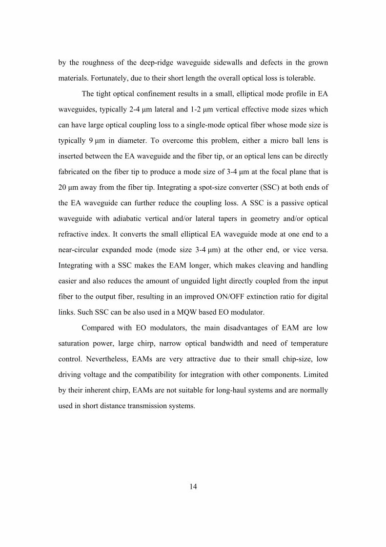
As mentioned in section 1.4, the InP-based MQW Mach-Zehnder modulator
has compact size, low driving voltage, zero or controllable chirp and the compatibility
for integration with other components. In addition, it is also suitable for advanced
modulation formats such as CS-RZ [23] and RZ-DPSK [24] for example. Its optical
insertion loss could also be reduced to a level comparable to that in LiNbO3-based
modulators. All these properties make it attractive for modulation rates well above
40 Gbit/s.
The modulator research group in the Fraunhofer-Institute for
Telecommunications Heinrich-Hertz-Institut has many years of research experience in
InP-based MQW Mach-Zehnder modulators. The electro-optical response of a
modulator of a preliminary version had achieved 20 GHz (cf. Fig. 1.7) and served as a
basis for further development. This work focuses on optimizing the electrical design
of the developed modulators and making them work up to 80 Gbit/s.
0 10 20 30 40 50
-9
-6
-3
0
e.o.
S21
[dB
]
Frequency [GHz]
S21 (#36B9)
20GHz
Fig. 1.7 Measured electro-optical response of a modulator
18
REFERENCES
[1] G. J. Holzmann and B. Pehrson, “The early history of data networks”, IEEE computer society press, Los Alsmitos, CA (1995)
[2] G. P. Agrawal, “Fiber-optic communication systems”, 3rd Ed., Wiley, New York (2002)
[3] R.G. Walker, “Low-voltage, 50 Ω, GaAs/AlGaAs travelling-wave modulator with bandwidth exceeding 25 GHz”, Electron. Lett. 25, 1549-1550 (1989).
[4] S. L. Chuang, “Physics of Optoelectronic Devices”, Wiley, 487-488 (1995)
[5] P. A. Morton, R. A. Logan, T. Tanbun-Ek, P. F. Sciortino, Jr, A. M. Sergent, R. K. Montgomery, and B. T. Lee, “25 GHz bandwidth 1.55 μm GaInAsP p-doped strained multiquantum well lasers,” Electron. Lett. 28, 2156–2157 (1992).
[6] S. Weiser, E. C. Larkins, K. Czotscher, w. Benz, J. Daleiden, J. Fleissner, M. Maier, J. D. Ralston, B. Romero, A. Schonfelder and J. Rosenzweig, “ 37 GHz direct modulation bandwidth in short-cavity InGaAs/GaAs MQW lasers with C-doped active regions,” paper SCL1.1, IEEE Lasers and Electro-Optic Society Annual Meeting, San Jose, CA, Oct. 30- Nov. 2, (1995)
[7] N. K. Dutta, N. A. Olsson, L. A. Koszi, P. Besomi, R. B. Wilson, and R. J. Nelson, “Frequency chirp under current modulation in InGaAsP injection lasers,” J. Appl. Phys. 56, 2167-2169 (1984).
[8] K. Noguchi, O. Mitomi, and H. Miyazawa, “Millimeter-Wave Ti:LiNbO3 Optical Modulators, ” IEEE J. Lightwave Technology, 16, 615-619 (1998)
[9] T. Yamannka, “High-performance InP-based optical modulators”, OWC1, OFC2006
[10] M. Lee, H. E. Katz, C. E. D. M. Gill, P. Gopalan, J. D. Heber and D. J. McGee, “Broadband Modulation of light by using an electro-optic polymer,” Science, 298, 1401-1403 (2002)
[11] S. Kalluri, M. Ziari, A. Chen, V. Chuyanov, W. H. Steier, D. Chen, B. Jalali, H. Fetterman, and L. R. Dalton, “Monolithic integration of waveguide polymer electrooptic modulators on VLSI circuitry,” IEEE Photon. Technol. Lett. 8, 644-646 (1996)
[12] R. A. Soref, “Silicon-based optoelectronics,” Proc. IEEE 81, 1687-1706 (1993)
[13] R. A. Soref and B. R. Bennett, “Electro optical effects in silicon,” IEEE J. Quantum Electron, QE-23, 123-129 (1987)
[14] C. K. Tang and G. T. Reed, “Highly efficient optical phase modulator in SOI waveguides,” Electron. Lett. 31, 451-452 (1995)
19
[15] P. Dainesi, “CMOS compatible fully integrated Mach-Zehnder interferometer in SOI technology,” IEEE Photon. Technol. Lett. 12, 660-662 (2000)
[16] A. Liu, R. Jones, L. Liao, D. Samara-Rubio, D. Rubin, O. Cohen, R. Nicolaescu, and M. Paniccia, “A high-speed silicon optical modulator based on a metal-oxide-semiconductor capacitor,” Nature 427, 615-618 (2004)
[17] L. Liao, “High-speed silicon Mach-Zehnder modulator,” Opt. Express 13, 3129 (2005)
[18] Y. Kuo, Y. Lee, Y. Ge, S. Ren, J. E. Roth, T. I. Kamins, D. A. B. Miller, and J. S. Harris, “Strong quantum-confined Stark effect in germanium quantum-well structures on silicon,” Nature 437, 1334-1336 (2005)
[19] K. Wakita, I. Kotaka, H. Asai, M. Okamoto, Y. Kondo, and M. Naganuma, “High-speed and low-drive voltage monolithic multiple quantum-well modulator/DFB laser light source,” IEEE Photon. Technol. Lett. 4, 16-18, (1992)
[20] N. Souli, A. Ramdane, F. Devaux, A. Ougazzaden, and S. Slempkes, “Tandem of electroabsorption modulators integrated with distributed feedback laser and optical amplifier for 20-Gbit/s pulse generation and coding at 1.5 μm,” in Proc. OFC’97 Tech. Dig. (Optical Fiber Communication), 6, paper WG6, 141-142 (1997)
[21] K. Schuh, “85.4Gbit/s ETDM transmission over 401 km SSMF applying UFEC”, ECOC2005 Th4.1.4, (2005)
[22] Peter J. Winzer, “107Gb/s optical ETDM transmitter for 100 G Ethernet transport”, ECOC2005 Th4.1.1, (2005)
[23] Y. Miyamoto, “320 Gbit/s (8x40 Gbit/s) WDM transmission over 367 km with 120 km repeater spacing using carrier-suppressed return-to-zero format,” Electronics Lett. 35, 2041-2042 (1999)
[24] A. H. Gnauck, “2.5 Tb/s (64x42.7 Gbit/s) transmission over 40x100 km NZDSF using RZ-DPSK format and all-Raman-amplified spans,” in Technical Digest of Optical Fiber Communication Conference (OFC2002) , Post-deadline paper, FC2 (2002).

20
21
Chapter 2
Basic Theory
The traveling-wave electrode Mach-Zehnder modulator is an electro-optic
device. To design and optimize such a device, it involves the knowledge of
semiconductor, high frequency microwave, and electro-optical effects. All of these
will be introduced briefly in this chapter.
2.1 COPLANAR LINES
The term coplanar lines is used for those transmission lines where all the
conductors are in the same plane, namely on the top of the dielectric substrate.
Coplanar waveguide (CPW) (cf. Fig. 2.1a) and coplanar strips (CPS) (cf. Fig. 2.2a) are
coplanar lines [1]. A distinct advantage of these two types of transmission line lies in
the fact that mounting lumped components in shunt or series configuration is much
easier. Drilling holes or slots through the substrates is not needed.
(a) CPW geometry (b) Electric and magnetic field distribution
Fig. 2.1 CPW geometry and corresponding electric and magnetic field distribution [1]
As shown in Fig. 2.1(a), CPW consists of two slots each of width w printed on
a dielectric substrate. The spacing between the slots is denoted by s. The electric and
magnetic field configurations for quasi-static approximation are shown in Fig. 2.1(b).
22
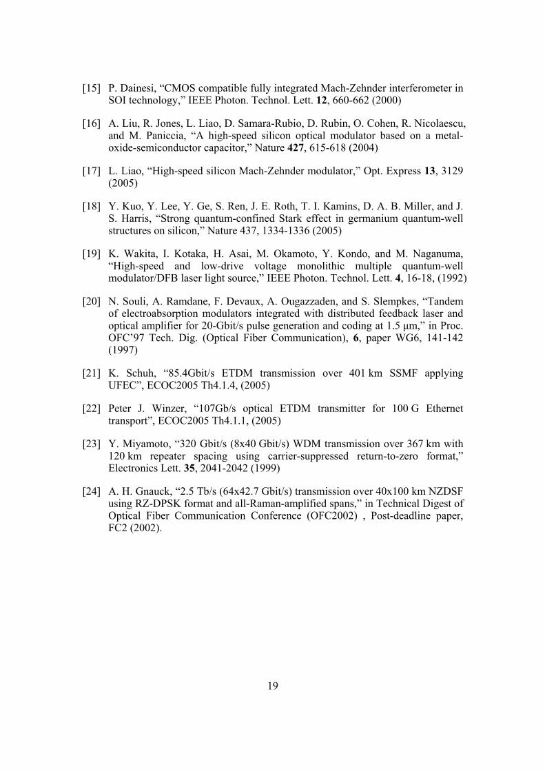
The configuration of CPS, which is complementary to the CPW, is shown in
Fig. 2.2(a). CPS consists of two strips, generally of equal width w on a dielectric
substrate. The spacing between the strips is denoted by s. The electric and magnetic
field configurations are shown in Fig. 2.2(b).
(a) CPS geometry (b) Electric and magnetic field distribution
Fig. 2.2 CPS geometry and corresponding electric and magnetic field distribution [1]
Sometimes, it is also desirable to use an asymmetric CPS (cf. Fig. 2.3) to adjust
the characteristic impedance by changing the width of one of the strips while keeping
the width of the other strip and the slot width fixed.
Fig. 2.3 Asymmetric CPS
CPW and CPS support quasi-TEM modes and have been analysed using quasi-
static as well as full-wave methods. Expressions for characteristic impedance Z0 and
effective dielectric constant εreff of CPW, CPS and asymmetric CPS are given in
table 2.1.
23
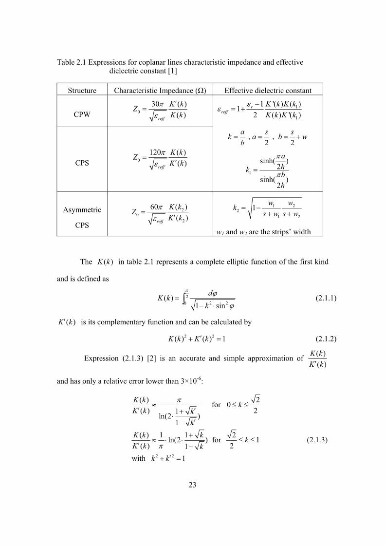
Table 2.1 Expressions for coplanar lines characteristic impedance and effective dielectric constant [1]
Structure Characteristic Impedance (Ω) Effective dielectric constant
CPW 030 ( )
( )reff
K kZK k
πε
′=
CPS 0120 ( )
( )reff
K kZK k
πε
=′
1
1
1 '( ) ( )12 ( ) '( )
rreff
K k K kK k K k
εε −= +
, , 2 2
a s sk a b wb
= = = +
1
sinh( )2
sinh( )2
ahk bh
π
π=
Asymmetric
CPS
20
2
( )60( )reff
K kZK k
πε
=′
1 22
1 2
1 w wks w s w
= −+ +
w1 and w2 are the strips’ width
The )(kK in table 2.1 represents a complete elliptic function of the first kind
and is defined as
22 20
( )1 sin
dK kk
π ϕϕ
=− ⋅
∫ (2.1.1)
( )K k′ is its complementary function and can be calculated by
2 2( ) ( ) 1K k K k′+ = (2.1.2)
Expression (2.1.3) [2] is an accurate and simple approximation of ( )( )
K kK k′
and has only a relative error lower than 3×10⁻⁶:
2 2
( ) 2 for 0( ) 21ln(2 )
1( ) 1 1 2ln(2 ) for 1 ( ) 21
with 1
K k kK k k
kK k k kK k k
k k
π
π
≈ ≤ ≤′ ′+
⋅′−
+≈ ⋅ ⋅ ≤ ≤
′ −′+ =
(2.1.3)
24
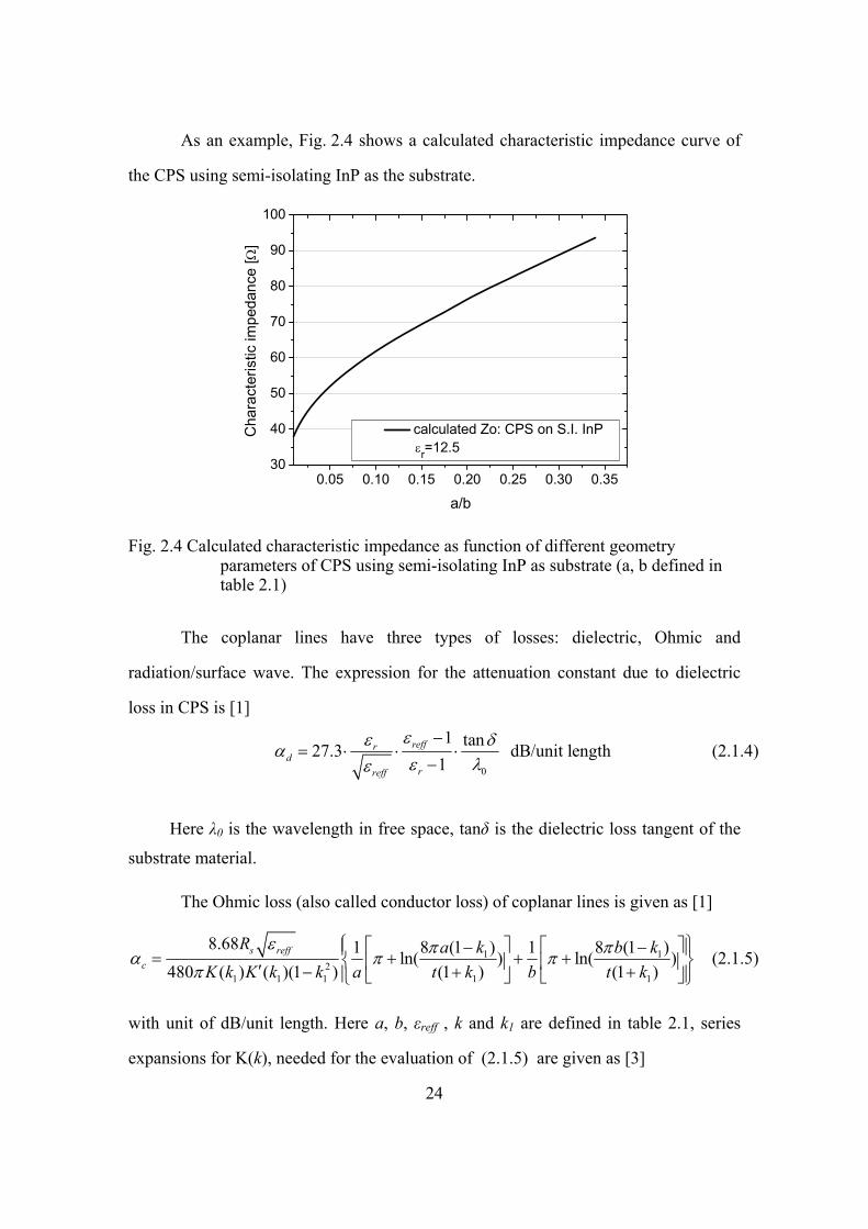
As an example, Fig. 2.4 shows a calculated characteristic impedance curve of
the CPS using semi-isolating InP as the substrate.
0.05 0.10 0.15 0.20 0.25 0.30 0.3530
40
50
60
70
80
90
100
Cha
ract
eris
tic im
peda
nce
[Ω]
a/b
calculated Zo: CPS on S.I. InP εr=12.5
Fig. 2.4 Calculated characteristic impedance as function of different geometry parameters of CPS using semi-isolating InP as substrate (a, b defined in table 2.1)
The coplanar lines have three types of losses: dielectric, Ohmic and
radiation/surface wave. The expression for the attenuation constant due to dielectric
loss in CPS is [1]
0
1 tan27.3 dB/unit length1
reffrd
rreff
εε δαε λε
−= ⋅ ⋅ ⋅
− (2.1.4)
Here λ0 is the wavelength in free space, tanδ is the dielectric loss tangent of the
substrate material.
The Ohmic loss (also called conductor loss) of coplanar lines is given as [1]
1 12
1 1 1 1 1
8.68 8 (1 ) 8 (1 )1 1ln( ) ln( ) 480 ( ) ( )(1 ) (1 ) (1 )
s reffc
R a k b kK k K k k a t k b t k
ε π πα π ππ
⎧ ⎫⎡ ⎤ ⎡ ⎤− −⎪ ⎪= + + +⎨ ⎬⎢ ⎥ ⎢ ⎥′ − + +⎪ ⎪⎣ ⎦ ⎣ ⎦⎩ ⎭ (2.1.5)
with unit of dB/unit length. Here a, b, εreff , k and k1 are defined in table 2.1, series
expansions for K(k), needed for the evaluation of (2.1.5) are given as [3]
25
( )
2 3 42 2 2 2
2 4 6
for 0 0.707
( ) 1 2 9 50 306.25 ...2 8 8 8 8
for 0.707 1
9 7 25 37( ) 1 ...2 4 6 2 4 30 2
4where ln
k
k k k kK k
k
k k kK k p p p p
pk
π
≤ ≤
⎧ ⎫⎛ ⎞ ⎛ ⎞ ⎛ ⎞ ⎛ ⎞⎪ ⎪= + + + + +⎨ ⎬⎜ ⎟ ⎜ ⎟ ⎜ ⎟ ⎜ ⎟⎝ ⎠ ⎝ ⎠ ⎝ ⎠ ⎝ ⎠⎪ ⎪⎩ ⎭
≤ ≤
′ ′ ′⎛ ⎞ ⎛ ⎞⎛ ⎞ ⎛ ⎞⎛ ⎞= + − + − + − +⎜ ⎟ ⎜ ⎟⎜ ⎟ ⎜ ⎟⎜ ⎟⎝ ⎠ ⎝ ⎠⎝ ⎠ ⎝ ⎠⎝ ⎠
⎛ ⎞= ⎜ ′⎝⎟⎠
(2.1.6)
In addition to the dielectric and Ohmic losses, coupling of power to surface
waves and radiation from unwanted (parasitic) modes also contribute to the total loss
of coplanar lines. Coplanar lines with finite thickness substrate can also be leaky.
However, if the substrate thickness h according to [4]
00.12
r
h λε⋅
< (2.1.7)
power leakage can be avoided since the cutoff frequency of the surface modes is
pushed above the operating frequency. That is, for InP substrate and work frequency of
40 GHz, the substrate thickness h should be smaller than 255 μm.
2.2 TRANSMISSION LINE THEORY
At frequencies where the wavelength is several orders of magnitude larger than
the greatest dimensions of the circuit or system being examined, conventional circuit
elements such as capacitors, inductors, resistors and transistors are the basic building
blocks for the circuits or systems. The description or analysis of such circuits may be
adequately carried out in terms of loop currents and node voltages without
consideration of propagation effects. However, as the frequency is raised to a point
where the wavelength is no longer large compared to the circuit dimensions,
propagation effects can no longer be ignored [5]. This problem can be solved by using
26
transmission line theory. On the other hand, coplanar lines are also transmission lines.
Hence, the transmission line theory is the basis for analyzing the high-speed traveling-
wave modulator.
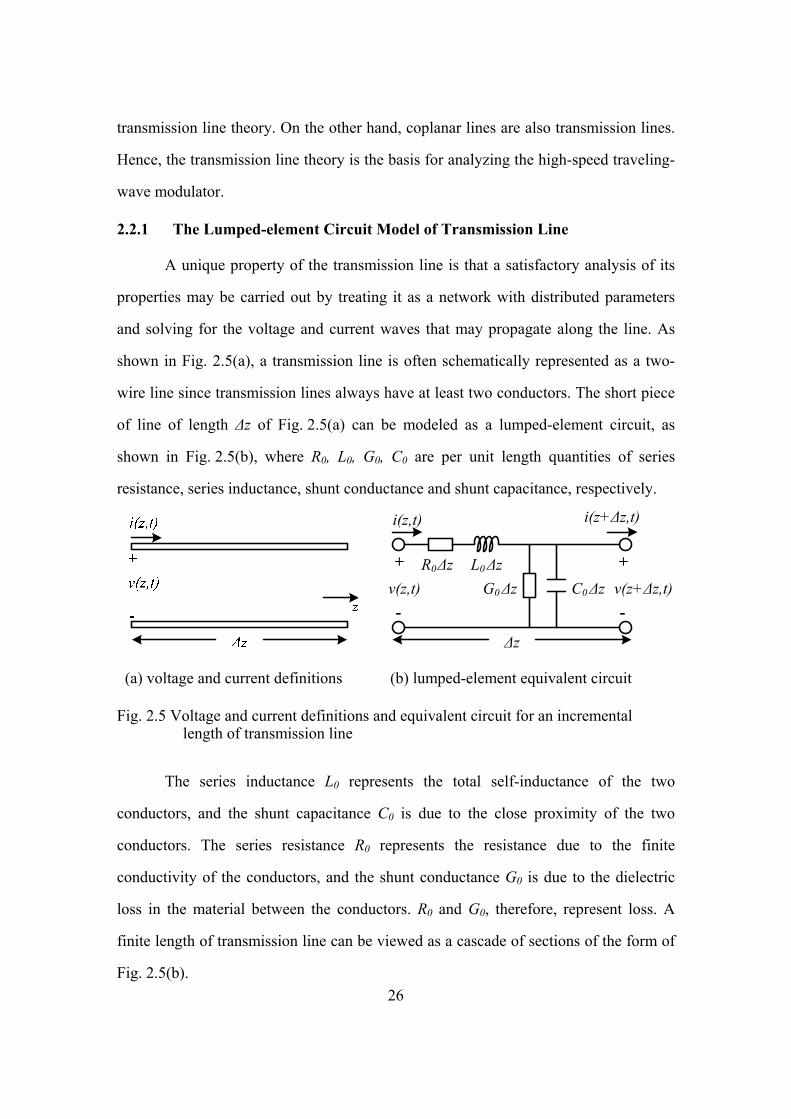
2.2.1 The Lumped-element Circuit Model of Transmission Line
A unique property of the transmission line is that a satisfactory analysis of its
properties may be carried out by treating it as a network with distributed parameters
and solving for the voltage and current waves that may propagate along the line. As
shown in Fig. 2.5(a), a transmission line is often schematically represented as a two-
wire line since transmission lines always have at least two conductors. The short piece
of line of length Δz of Fig. 2.5(a) can be modeled as a lumped-element circuit, as
shown in Fig. 2.5(b), where R0, L0, G0, C0 are per unit length quantities of series
resistance, series inductance, shunt conductance and shunt capacitance, respectively.
Δz
+
-v(z,t)
i(z,t)
L0ΔzG0Δz
R0ΔzC0Δz
+
-v(z+Δz,t)
i(z+Δz,t)
(a) voltage and current definitions (b) lumped-element equivalent circuit
Fig. 2.5 Voltage and current definitions and equivalent circuit for an incremental length of transmission line
The series inductance L0 represents the total self-inductance of the two
conductors, and the shunt capacitance C0 is due to the close proximity of the two
conductors. The series resistance R0 represents the resistance due to the finite
conductivity of the conductors, and the shunt conductance G0 is due to the dielectric
loss in the material between the conductors. R0 and G0, therefore, represent loss. A
finite length of transmission line can be viewed as a cascade of sections of the form of
Fig. 2.5(b).
27
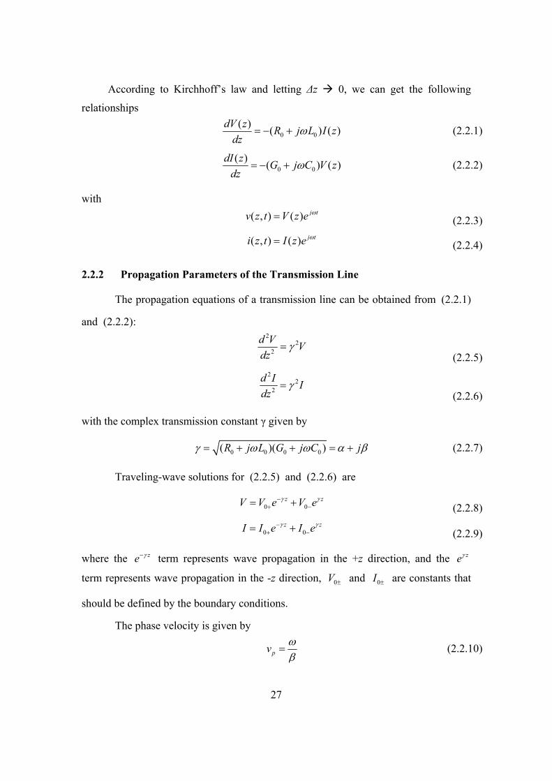
According to Kirchhoff’s law and letting Δz 0, we can get the following
relationships
0 0( ) ( ) ( )dV z R j L I z
dzω= − + (2.2.1)
0 0( ) ( ) ( )dI z G j C V z
dzω= − + (2.2.2)
with
( , ) ( ) j tv z t V z e ω= (2.2.3)
( , ) ( ) j ti z t I z e ω= (2.2.4)
2.2.2 Propagation Parameters of the Transmission Line
The propagation equations of a transmission line can be obtained from (2.2.1)
and (2.2.2):
22
2
d V Vdz
γ= (2.2.5)
22
2
d I Idz
γ= (2.2.6)
with the complex transmission constant γ given by
0 0 0 0( )( )R j L G j C jγ ω ω α β= + + = + (2.2.7)
Traveling-wave solutions for (2.2.5) and (2.2.6) are
0 0z zV V e V eγ γ−
+ −= + (2.2.8)
0 0z zI I e I eγ γ−
+ −= + (2.2.9)
where the ze γ− term represents wave propagation in the +z direction, and the zeγ
term represents wave propagation in the -z direction, 0V ± and 0I ± are constants that
should be defined by the boundary conditions.
The phase velocity is given by
pv ωβ
= (2.2.10)
28
The characteristic impedance Z0 of the transmission line can be defined as [5]
0 00
0 0
R j LZG j C
ωω
+=
+ (2.2.11)
As shown in Fig. 2.6, the transmission line with characteristic impedance Z0,
propagation constant γ, and length l can be described as a two-port network. The
transmission matrix (also called ABCD matrix, definition in Appendix A) of this two-
port network is [6]
0
0
cosh( ) sinh( )1 sinh( ) cosh( )
l Z lA B
l lC DZ
γ γ
γ γ
⎡ ⎤⎡ ⎤ ⎢ ⎥=⎢ ⎥ ⎢ ⎥⎣ ⎦ ⎢ ⎥⎣ ⎦
(2.2.12)
Fig. 2.6 A two-port network model for the transmission line
One can get the transmission matrix by converting the measured scattering
matrix as follows [6]
11 22 12 21 11 22 12 21
21 21
11 22 12 21 11 22 12 21
21 21
(1 )(1 ) (1 )(1 )2 2
(1 )(1 ) (1 )(1 )12 2
r
r
S S S S S S S SZS SA B
C D S S S S S S S SZ S S
+ − + + + −⎡ ⎤⎢ ⎥⎡ ⎤ ⎢ ⎥=⎢ ⎥ − − − − + +⎢ ⎥⎣ ⎦⎢ ⎥⎣ ⎦
(2.2.13)
here Zr is the reference impedance used in the measurement and is normally equal to
50 Ω.
The propagation parameter γ and the characteristic impedance Z0 can be
calculated from (2.2.12):
ln( )
2A D BC
lγ
++
= (2.2.14)
29
0BZC
= (2.2.15)
From (2.2.7) and (2.2.11), the R0, L0, G0, C0 can be calculated by (2.2.16)
using the propagation parameter γ and characteristic impedance Z0, respectively.
00 0 0
00 0
0
Im( ) R = Re( )
Im( ) G = Re( )
γ γωγ
γω
⋅= ⋅
=
ZL Z
ZCZ
(2.2.16)
2.2.3 Analysis of the Periodically Loaded Transmission Line
The periodically loaded transmission line (cf. Fig 2.7) may have a lower phase
velocity than the smooth transmission line. This property is used as a slow-wave
property in modulator design.
Fig. 2.7 A periodically loaded transmission line
Fig. 2.8 Equivalent circuit of a unit cell in Fig. 2.7, uniform transmission line with shunt element in center
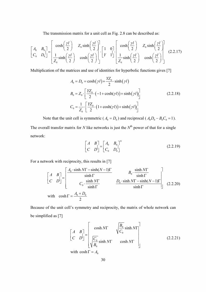
30
The transmission matrix for a unit cell as Fig. 2.8 can be described as:
0 00 0
0 0
0 0
cosh sinh cosh sinh1 02 2 2 2
11 1sinh cosh sinh cosh2 2 2 2
l l l lZ ZA BC D Yl l l l
Z Z
γ γ γ γ
γ γ γ γ
⎡ ⎤ ⎡ ⎤⎛ ⎞ ⎛ ⎞ ⎛ ⎞ ⎛ ⎞⎜ ⎟ ⎜ ⎟ ⎜ ⎟ ⎜ ⎟⎢ ⎥ ⎢ ⎥⎡ ⎤ ⎡ ⎤⎝ ⎠ ⎝ ⎠ ⎝ ⎠ ⎝ ⎠⎢ ⎥ ⎢ ⎥= ⋅ ⋅⎢ ⎥ ⎢ ⎥⎢ ⎥ ⎢ ⎥⎛ ⎞ ⎛ ⎞ ⎛ ⎞ ⎛ ⎞⎣ ⎦⎣ ⎦
⎢ ⎥ ⎢ ⎥⎜ ⎟ ⎜ ⎟ ⎜ ⎟ ⎜ ⎟⎝ ⎠ ⎝ ⎠ ⎝ ⎠ ⎝ ⎠⎣ ⎦ ⎣ ⎦
(2.2.17)
Multiplication of the matrices and use of identities for hyperbolic functions gives [7]
( ) ( )
( ) ( )
( ) ( )
00 0
00 0
00
0
cosh sinh2
1 cosh( ) sinh2
1 1 cosh( ) sinh2
YZA D l l
YZB Z l l
YZC l lZ
γ γ
γ γ
γ γ
= = + ⋅
⎡ ⎤= ⋅ ⋅ − + +⎢ ⎥⎣ ⎦
⎡ ⎤= ⋅ ⋅ + +⎢ ⎥⎣ ⎦
(2.2.18)
Note that the unit cell is symmetric ( 0 0A D= ) and reciprocal ( 0 0 0 0 1A D B C− = ).
The overall transfer matrix for N like networks is just the Nth power of that for a single
network:
0 0
0 0
NA BA BC DC D
⎡ ⎤⎡ ⎤= ⎢ ⎥⎢ ⎥
⎣ ⎦ ⎣ ⎦ (2.2.19)
For a network with reciprocity, this results in [7]
00
00
0 0
sinh sinh( 1) sinhsinh sinh
sinh sinh( 1)sinhsinh sinh
with cosh2
A N N NBA BC D D N NNC
A D
⋅ Γ − − Γ Γ⎡ ⎤⋅⎢ ⎥⎡ ⎤ Γ Γ= ⎢ ⎥⎢ ⎥ ⋅ Γ − − ΓΓ⎣ ⎦ ⎢ ⎥⋅⎢ ⎥Γ Γ⎣ ⎦
+Γ =
(2.2.20)
Because of the unit cell’s symmetry and reciprocity, the matrix of whole network can
be simplified as [7]
0
0
0
0
0
cosh sinh
sinh cosh
with cosh
BN NCA B
C D C N NB
A
⎡ ⎤Γ Γ⎢ ⎥
⎡ ⎤ ⎢ ⎥=⎢ ⎥ ⎢ ⎥⎣ ⎦ ⎢ ⎥Γ Γ⎢ ⎥⎣ ⎦Γ =
(2.2.21)
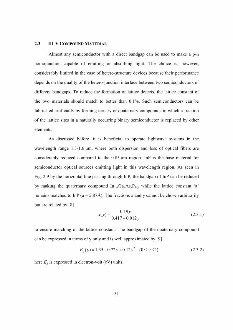
31
2.3 III-V COMPOUND MATERIAL
Almost any semiconductor with a direct bandgap can be used to make a p-n
homojunction capable of emitting or absorbing light. The choice is, however,
considerably limited in the case of hetero-structure devices because their performance
depends on the quality of the hetero-junction interface between two semiconductors of
different bandgaps. To reduce the formation of lattice defects, the lattice constant of
the two materials should match to better than 0.1%. Such semiconductors can be
fabricated artificially by forming ternary or quaternary compounds in which a fraction
of the lattice sites in a naturally occurring binary semiconductor is replaced by other
elements.
As discussed before, it is beneficial to operate lightwave systems in the
wavelength range 1.3-1.6 μm, where both dispersion and loss of optical fibers are
considerably reduced compared to the 0.85 μm region. InP is the base material for
semiconductor optical sources emitting light in this wavelength region. As seen in
Fig. 2.9 by the horizontal line passing through InP, the bandgap of InP can be reduced
by making the quaternary compound In1-xGaxAsyP1-y while the lattice constant ‘a’
remains matched to InP (a = 5.87Å). The fractions x and y cannot be chosen arbitrarily
but are related by [8]
0.19( )0.417 0.012
yx yy
=−
(2.3.1)
to ensure matching of the lattice constant. The bandgap of the quaternary compound
can be expressed in terms of y only and is well approximated by [9]
2( ) 1.35 0.72 0.12 (0 1)gE y y y y= − + ≤ ≤ (2.3.2)
here Eg is expressed in electron-volt (eV) units.
32
Fig. 2.9 Lattice constant and bandgap energies of ternary and quaternary compounds formed by using III-V group semiconductors [10]
The wavelength of the emitted light is determined by the bandgap since the
photon energy is approximately equal to the bandgap energy. The corresponding light
wavelength, λ, can be obtained using [10]
ghcE hνλ
≈ = (2.3.3)
where h is the Planck constant, ν is the frequency of the photon and c is the speed of
light in free space. If Eg is expressed in eV, the light wavelength in microns (μm) is
given by [10]
1.24
gEλ = (2.3.4)
The smallest bandgap of In1-xGaxAsyP1-y occurs for y=1. The corresponding
ternary compound In0.54Ga0.46 As emits light near 1.65 μm (Eg=0.75eV). By a suitable
choice of the mixing fractions x and y, In1-xGaxAsyP1-y sources can be designed to
operate in the wide wavelength range 1.0-1.65 μm that includes the region 1.3-1.6μm,
which is important for optical communication systems.
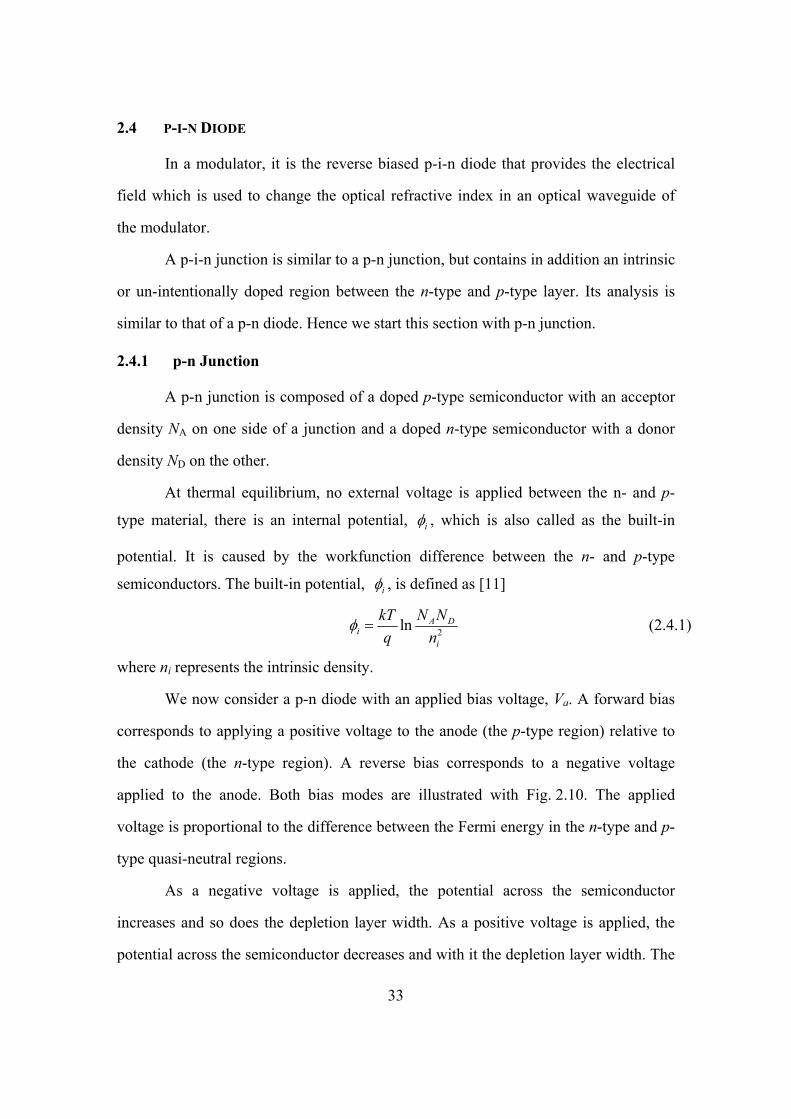
33
2.4 P-I-N DIODE
In a modulator, it is the reverse biased p-i-n diode that provides the electrical
field which is used to change the optical refractive index in an optical waveguide of
the modulator.
A p-i-n junction is similar to a p-n junction, but contains in addition an intrinsic
or un-intentionally doped region between the n-type and p-type layer. Its analysis is
similar to that of a p-n diode. Hence we start this section with p-n junction.
2.4.1 p-n Junction
A p-n junction is composed of a doped p-type semiconductor with an acceptor
density NA on one side of a junction and a doped n-type semiconductor with a donor
density ND on the other.
At thermal equilibrium, no external voltage is applied between the n- and p-
type material, there is an internal potential, iφ , which is also called as the built-in
potential. It is caused by the workfunction difference between the n- and p-type
semiconductors. The built-in potential, iφ , is defined as [11]
2ln A Di
i
N NkTq n
φ = (2.4.1)
where ni represents the intrinsic density.
We now consider a p-n diode with an applied bias voltage, Va. A forward bias
corresponds to applying a positive voltage to the anode (the p-type region) relative to
the cathode (the n-type region). A reverse bias corresponds to a negative voltage
applied to the anode. Both bias modes are illustrated with Fig. 2.10. The applied
voltage is proportional to the difference between the Fermi energy in the n-type and p-
type quasi-neutral regions.
As a negative voltage is applied, the potential across the semiconductor
increases and so does the depletion layer width. As a positive voltage is applied, the
potential across the semiconductor decreases and with it the depletion layer width. The
34
total potential across the semiconductor equals the built-in potential minus the applied
voltage, or:
i aVφ φ= − (2.4.2)
Fig. 2.10 p-n junction under (a) reverse and (b) forward bias
The full-depletion approximation assumes that the depletion region around the
junction has well-defined edges. It also assumes that the transition between the
depleted and the quasi-neutral region is abrupt. We define the quasi-neutral region as
the region adjacent to the depletion region where the electric field is small and the free
carrier density is close to the net doping density.
We will therefore start the electrostatic analysis using an abrupt charge density
profile, while introducing two unknowns, namely the depletion layer width in the p-
type region, xp, and the depletion region width in the n-type region, xn. The sum of the
two depletion layer widths in each region is the total depletion layer width xd, or:
d n px x x= + (2.4.3)
Since in thermal equilibrium the electric field in the neutral regions of the
semiconductor must be zero, the total negative charge per unit area in the p side must
be precisely equal to the total positive charge per unit area in the n side. This provides
the first relationship between the two unknowns, xp and xn, namely [11]:
D n A pN x N x= (2.4.4)
35
We can then combine (2.4.3) with (2.4.4) for the total depletion-layer width,
xd, yielding:
An d
A D
Nx xN N
=+
(2.4.5)
and Dp d
A D
Nx xN N
=+
(2.4.6)
The total potential across the semiconductor must equal the difference between
the built-in potential and the applied voltage, which provides a second relation
between xp and xn, namely [11]:
22
2 2A pD n
i as s
qN xqN xVφε ε
− = + (2.4.7)
here εs is the permittivity of the semiconductor.
The depletion layer width is obtained by substituting the expressions for xp and
xn, (2.4.5) and (2.4.6), into the expression for the potential across the depletion
region, yielding [11]:
2 1 1( )( )sd i a
A D
x Vq N Nε φ= + − (2.4.8)
from which the solutions for the individual depletion layer widths, xp and xn are
obtained:
2 1 ( )s An i a
D A D
Nx Vq N N Nε φ= −
+ (2.4.9)
2 1 ( )s Dp i a
A A D
Nx Vq N N Nε φ= −
+ (2.4.10)
Any variation of the charge within a p-n diode with an applied voltage
variation yields a capacitance, which must be added to the circuit model of a p-n diode.
This capacitance related to the depletion layer charge in a p-n diode is called the
junction capacitance.
36
The capacitance versus applied voltage is by definition the change in charge for
a change in applied voltage, or:
( )( ) aa
a
dQ VC VdV
= (2.4.11)
The absolute value sign is added in the definition so that either the positive or
the negative charge can be used in the calculation, as they are equal in magnitude.
Using n D nQ qN x= and (2.4.9) one obtains [11]:
2( )
s A Dj
i a A D
q N NCV N N
εφ
=− +
(2.4.12)
A comparison with (2.4.8), which provides the depletion layer width, xd, as a
function of voltage, reveals that the expression for the junction capacitance (per unit
surface area), Cj, seems to be identical to that of a parallel plate capacitor, namely:
sj
d
Cxε
= (2.4.13)
The difference, however, is that the depletion layer width and hence the
capacitance is voltage dependent. The parallel plate expression still applies since
charge is only added at the edge of the depletion regions. The distance between the
added negative and positive charge equals the depletion layer width, xd.
The capacitance of a p-n diode is frequently expressed as a function of the zero
bias capacitance, Cj0 [11] :
2
1 2 ( )A Di a
j s A D
N N VC q N N
φε
+= − (2.4.14)
where
2
1( ) 2jC A D
a s A D
d N NdV q N Nε
+= − (2.4.15)
A capacitance versus voltage measurement (C-V measurement) can be used to
obtain the built-in voltage and the doping density of a one-sided p-n diode. When
plotting the inverse of the capacitance squared, one expects a linear dependence as
expressed by:
37
2
12 1 , if ( )
j
D A Ds C
a
N N NdqdV
ε= − (2.4.16)
The built-in voltage is obtained at the intersection of the 1/C2 curve and the
horizontal axis, while the doping density is obtained from the slope of the curve.
2.4.2 p-i-n junction
A p-i-n junction is similar to a p-n junction, but contains in addition an intrinsic
or un-intentionally doped region with thickness, di, between the n-type and p-type
layer. Such structure is typically used if one wants to increase the width of the
depletion region. In the modulator a wide depletion region is required for a large
overlap of the optical wave with the controlling electrical field.
The analysis is also similar to that of a p-n diode, although the potential across
the undoped region, φu, must be included in the analysis. (2.4.7) then becomes [11]:
n p u i aVφ φ φ φ+ + = − (2.4.17)
22
, , and 2 2
A p A p iD nn p u
s s s
qN x qN x dqN xφ φ φε ε ε
= = = (2.4.18)
while the charge in the n-type region still equals that in the p-type region, so that
(2.4.4) still holds: D n A pqN x qN x= (2.4.19)
From xn and xp, all other parameters of the p-i-n junction can be obtained. The
total depletion layer width, xd, is obtained from [11]:
2 2 ( )s A Dd n p i i i a
A D
N Nx x x d d Vq N Nε φ+
= + + = + − (2.4.20)
The capacitance of a p-i-n diode equals the series connection of the
capacitances of each region, simply by adding both depletion layer widths and the
width of the undoped region, and similar to p-n junction, the capacitance is voltage
dependent.
38
2.5 METAL-SEMICONDUCTOR CONTACTS
Metal-semiconductor contacts are an obvious component of any semiconductor
device. At the same time, such contacts cannot be assumed to have a resistance as low
as that of two connected metals. In particular, a large mismatch between the Fermi
energy of the metal and semiconductor can result a high-resistance rectifying contact.
A proper choice of materials can provide a low resistance Ohmic contact.
In the modulator, the contact between the gold and p-doped InP is an Ohmic
contact. Hence, we focus on Ohmic contact in this section.
2.5.1 Ohmic Contact
A metal-semiconductor junction results in an Ohmic contact (i.e. a contact with
voltage independent resistance) if the Schottky barrier height is zero or negative. In
such case, the carriers are free to flow in or out of the semiconductor so that there is a
minimal resistance across the contact. For an n-type semiconductor, this means that the
workfunction of the metal must be close to or smaller than the electron affinity of the
semiconductor. For a p-type semiconductor, it requires that the workfunction of the
metal must be close to or larger than the sum of the electron affinity and the bandgap
energy.
For an Ohmic contact, the contact resistivity, ρc, is given by [12]
20 cm
BKN
c c eφ
ρ ρ= ⋅ Ω⋅ (2.5.1)
where K and ρc0 are constants dependent upon metal and the semiconductor. ρc,
primarily depends upon the metal-semiconductor work function, ΦB, and doping
density, N, in the semiconductor.
Since the workfunction of most metals is less than 5 eV and a typical electron
affinity is about 4 eV, it can be problematic to find a metal that provides an Ohmic
contact to p-type semiconductors with a large bandgap. An alternate and more
practical contact is a tunnel contact. Such contacts do have a positive barrier at the
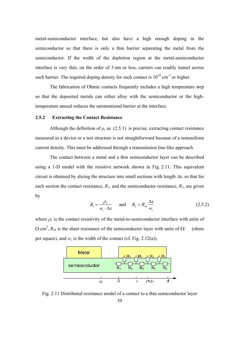
39
metal-semiconductor interface, but also have a high enough doping in the
semiconductor so that there is only a thin barrier separating the metal from the
semiconductor. If the width of the depletion region at the metal-semiconductor
interface is very thin, on the order of 3 nm or less, carriers can readily tunnel across
such barrier. The required doping density for such contact is 1019 cm-3 or higher.
The fabrication of Ohmic contacts frequently includes a high temperature step
so that the deposited metals can either alloy with the semiconductor or the high-
temperature anneal reduces the unintentional barrier at the interface.
2.5.2 Extracting the Contact Resistance
Although the definition of ρc as (2.5.1) is precise, extracting contact resistance
measured in a device or a test structure is not straightforward because of a nonuniform
current density. This must be addressed through a transmission line-like approach.
The contact between a metal and a thin semiconductor layer can be described
using a 1-D model with the resistive network shown in Fig. 2.11. This equivalent
circuit is obtained by slicing the structure into small sections with length Δx, so that for
each section the contact resistance, R1, and the semiconductor resistance, R2, are given
by
1 2 and csh
c c
xR R Rw x w
ρ Δ= =
⋅Δ (2.5.2)
where ρc is the contact resistivity of the metal-to-semiconductor interface with units of
Ω·cm2, Rsh is the sheet resistance of the semiconductor layer with units of Ω/ (ohms
per square), and wc is the width of the contact (cf. Fig. 2.12(a)).
Fig. 2.11 Distributed resistance model of a contact to a thin semiconductor layer
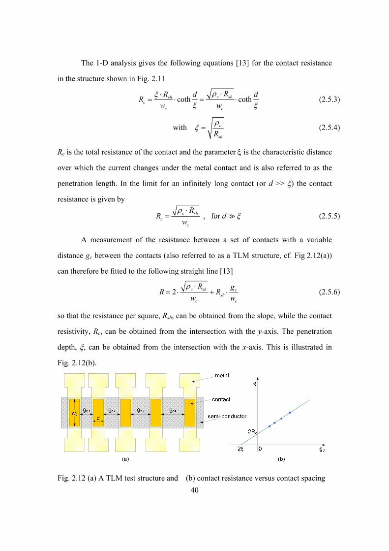
40
The 1-D analysis gives the following equations [13] for the contact resistance
in the structure shown in Fig. 2.11
coth cothc shshc
c c
RR d dRw w
ρξξ ξ
⋅⋅= ⋅ = ⋅ (2.5.3)
with c
shRρξ = (2.5.4)
Rc is the total resistance of the contact and the parameter ξ is the characteristic distance
over which the current changes under the metal contact and is also referred to as the
penetration length. In the limit for an infinitely long contact (or d >> ξ) the contact
resistance is given by
, for c shc
c
RR d
wρ
ξ⋅
= (2.5.5)
A measurement of the resistance between a set of contacts with a variable
distance gc between the contacts (also referred to as a TLM structure, cf. Fig 2.12(a))
can therefore be fitted to the following straight line [13]
2 c sh csh
c c
R gR Rw w
ρ ⋅= ⋅ + ⋅ (2.5.6)
so that the resistance per square, Rsh, can be obtained from the slope, while the contact
resistivity, Rc, can be obtained from the intersection with the y-axis. The penetration
depth, ξ, can be obtained from the intersection with the x-axis. This is illustrated in
Fig. 2.12(b).
Fig. 2.12 (a) A TLM test structure and (b) contact resistance versus contact spacing
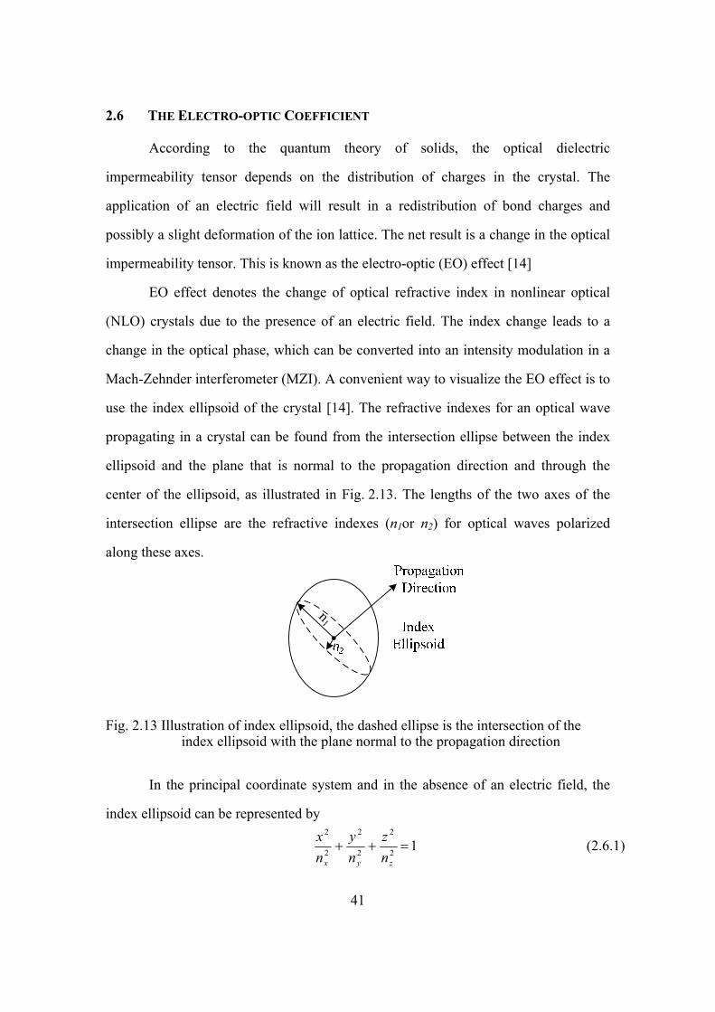
41
2.6 THE ELECTRO-OPTIC COEFFICIENT
According to the quantum theory of solids, the optical dielectric
impermeability tensor depends on the distribution of charges in the crystal. The
application of an electric field will result in a redistribution of bond charges and
possibly a slight deformation of the ion lattice. The net result is a change in the optical
impermeability tensor. This is known as the electro-optic (EO) effect [14]
EO effect denotes the change of optical refractive index in nonlinear optical
(NLO) crystals due to the presence of an electric field. The index change leads to a
change in the optical phase, which can be converted into an intensity modulation in a
Mach-Zehnder interferometer (MZI). A convenient way to visualize the EO effect is to
use the index ellipsoid of the crystal [14]. The refractive indexes for an optical wave
propagating in a crystal can be found from the intersection ellipse between the index
ellipsoid and the plane that is normal to the propagation direction and through the
center of the ellipsoid, as illustrated in Fig. 2.13. The lengths of the two axes of the
intersection ellipse are the refractive indexes (n1or n2) for optical waves polarized
along these axes.
n1
Fig. 2.13 Illustration of index ellipsoid, the dashed ellipse is the intersection of the index ellipsoid with the plane normal to the propagation direction
In the principal coordinate system and in the absence of an electric field, the
index ellipsoid can be represented by
12
2
2
2
2
2
=++zyx n
zny
nx (2.6.1)
42
where the directions of x, y and z are the principal dielectric axes with the
corresponding refractive indexes nx, ny and nz. After the electric field is applied, both
the size and the orientation of the index ellipsoid are changed. The equation of the
index ellipsoid is generally modified to [14]
2 2 22 2 2 2 2 21 2 3 4 5 6
1 1 1 1 1 12 2 2 1x y z yz zx xyn n n n n n
+ + + + + = (2.6.2)
Comparing (2.6.2) and (2.6.1), it is apparent that, without an applied electric field
2 2 2 2 2 2 2 2 21 2 3 4 5 6
1 1 1 1 1 1 1 1 1 , , , =0 x y zn n n n n n n n n
= = = = = (2.6.3)
After an electric field is applied, the above six terms may be changed. When
only the linear EO effect is considered, the change induced by the electric field ( , , )x y zE E E E= can be expressed as [14]
21
22
23
24
25
26
1
11 12 131
21 22 231
31 32 331
41 42 43
1 51 52 53
61 62 631
n
n
xn
yn
z
n
n
r r rr r r
Er r r
Er r r
Er r rr r r
Δ⎡ ⎤⎢ ⎥ ⎡ ⎤Δ⎢ ⎥ ⎢ ⎥
⎢ ⎥ ⎢ ⎥ ⎡ ⎤Δ⎢ ⎥ ⎢ ⎥ ⎢ ⎥=⎢ ⎥ ⎢ ⎥ ⎢ ⎥Δ⎢ ⎥ ⎢ ⎥ ⎢ ⎥⎣ ⎦⎢ ⎥ ⎢ ⎥Δ⎢ ⎥ ⎢ ⎥⎢ ⎥⎢ ⎥ ⎣ ⎦Δ⎢ ⎥⎣ ⎦
(2.6.4)
where the 6×3 matrix [rij] is called the electro-optic tensor, and its elements are called
electro-optic coefficients.
The values of index terms in (2.6.2) are now the sum of the original values in
(2.6.3) plus the corresponding changes in (2.6.4). For various crystals, due to the
crystal symmetry, some of the EO coefficients may be zero, and some of them may be
equal in value (or opposite in sign) [14]. With the EO tensor determined, the modified
index ellipsoid due to an arbitrary electric field can be found through (2.6.2)-(2.6.4),
and the refractive indexes for an arbitrary optical wave can be determined using the
index ellipsoid.
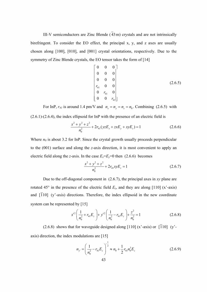
43
III-V semiconductors are Zinc Blende ( 43m) crystals and are not intrinsically
birefringent. To consider the EO effect, the principal x, y, and z axes are usually
chosen along [100], [010], and [001] crystal orientations, respectively. Due to the
symmetry of Zinc Blende crystals, the EO tensor takes the form of [14]
41
41
41
0 0 00 0 00 0 0
0 00 00 0
rr
r
⎡ ⎤⎢ ⎥⎢ ⎥⎢ ⎥⎢ ⎥⎢ ⎥⎢ ⎥⎢ ⎥⎢ ⎥⎣ ⎦
(2.6.5)
For InP, r41 is around 1.4 pm/V and 0x y zn n n n= = = . Combining (2.6.5) with
(2.6.1)-(2.6.4), the index ellipsoid for InP with the presence of an electric field is
2 2 2
4120
2 ( ) 1x y zx y z r yzE zxE xyE
n+ +
+ + + = (2.6.6)
Where n0 is about 3.2 for InP. Since the crystal growth usually proceeds perpendicular
to the (001) surface and along the z-axis direction, it is most convenient to apply an
electric field along the z-axis. In the case Ex=Ey=0 then (2.6.6) becomes
2 2 2
4120
2 1zx y z r xyE
n+ +
+ = (2.6.7)
Due to the off-diagonal component in (2.6.7), the principal axes in xy plane are
rotated 45° in the presence of the electric field Ez, and they are along [110] (x’-axis)
and [110] (y’-axis) directions. Therefore, the index ellipsoid in the new coordinate
system can be represented by [15]
2
2 241 412 2 2
0 0 0
1 1 1z zzx r E y r E
n n n⎛ ⎞ ⎛ ⎞
′ ′+ + − + =⎜ ⎟ ⎜ ⎟⎝ ⎠ ⎝ ⎠
(2.6.8)
(2.6.8) shows that for waveguide designed along [110] (x’-axis) or [110] (y’-
axis) direction, the index modulations are [15]
12
341 0 41 02
0
1 12y z zn r E n r n E
n
−
′
⎛ ⎞= − ≈ +⎜ ⎟
⎝ ⎠ (2.6.9)
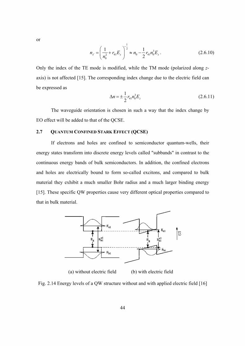
44
or
12
341 0 41 02
0
1 12x z zn r E n r n E
n
−
′
⎛ ⎞= + ≈ −⎜ ⎟
⎝ ⎠. (2.6.10)
Only the index of the TE mode is modified, while the TM mode (polarized along z-
axis) is not affected [15]. The corresponding index change due to the electric field can
be expressed as
341 0
12 zn r n EΔ = ± (2.6.11)
The waveguide orientation is chosen in such a way that the index change by
EO effect will be added to that of the QCSE.
2.7 QUANTUM CONFINED STARK EFFECT (QCSE)
If electrons and holes are confined to semiconductor quantum-wells, their
energy states transform into discrete energy levels called "subbands" in contrast to the
continuous energy bands of bulk semiconductors. In addition, the confined electrons
and holes are electrically bound to form so-called excitons, and compared to bulk
material they exhibit a much smaller Bohr radius and a much larger binding energy
[15]. These specific QW properties cause very different optical properties compared to
that in bulk material.
(a) without electric field (b) with electric field
Fig. 2.14 Energy levels of a QW structure without and with applied electric field [16]
45
Fig. 2.14 shows energy levels of a QW structure without and with applied
electric field which is perpendicular to the wells, i.e. along the direction of quantum-
well layer growth. Ee1 lines represent the 1st electron energy level, Eh1 lines represent
the 1st hole energy level. For the sake of simplicity, we will neglect the degeneracy of
the valence band as encountered in III-V semiconductors such as GaAs or InP for
example, and we will also neglect the effect of strain although QWs are frequently
grown under strain. Even under these simplifying assumptions the main arguments will
still remain valid.
Curves in the well represent the envelope wavefunctions for electrons and
holes. As illustrated in Fig. 2.14, two main changes occur when an electric field is
applied across a QW. First, the energy levels of the electrons Ee and those of the holes
Eh are lowered, and as a consequence the exciton absorption peak shifts to lower
energies (longer wavelengths). Second, due to the tilted band diagram the electrons
and the holes get spatially separated which reduces the overlap of the electron and hole
wavefunctions. This reduced overlap lowers the exciton binding energy which tends to
introduce a blue-shift of the exciton absorption, however, this effect is significantly
less pronounced than the red-shift due to the field-induced change of the energy levels
(subbands). Furthermore, the exciton linewidth is also broadened due to the presence
of the electric field. Altogether, an applied electric field causes a significant shift of the
optical absorption to longer wavelengths (compared to the case without applied
electric field), and this effect is known as the QCSE.
Due to the strong exciton resonance, QCSE induced absorption change is much
larger than that of the Franz-Keldysh effect (FKE).
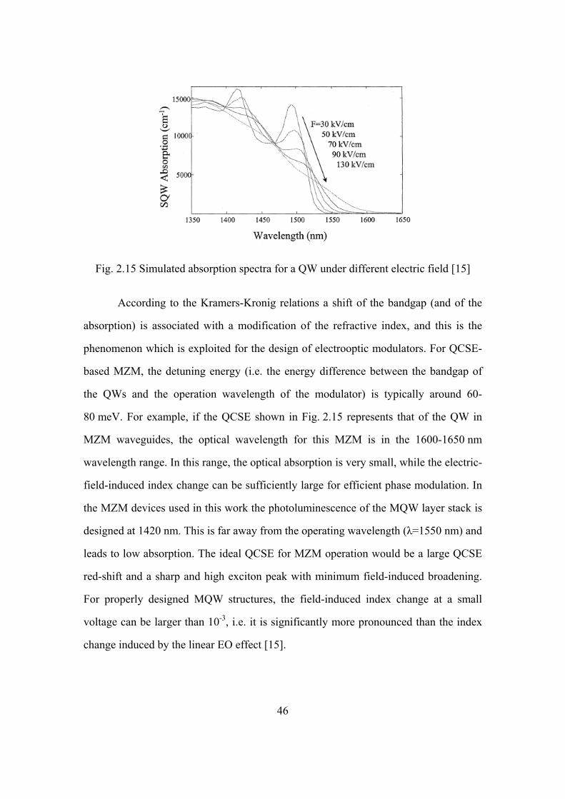
46
Fig. 2.15 Simulated absorption spectra for a QW under different electric field [15]
According to the Kramers-Kronig relations a shift of the bandgap (and of the
absorption) is associated with a modification of the refractive index, and this is the
phenomenon which is exploited for the design of electrooptic modulators. For QCSE-
based MZM, the detuning energy (i.e. the energy difference between the bandgap of
the QWs and the operation wavelength of the modulator) is typically around 60-
80 meV. For example, if the QCSE shown in Fig. 2.15 represents that of the QW in
MZM waveguides, the optical wavelength for this MZM is in the 1600-1650 nm
wavelength range. In this range, the optical absorption is very small, while the electric-
field-induced index change can be sufficiently large for efficient phase modulation. In
the MZM devices used in this work the photoluminescence of the MQW layer stack is
designed at 1420 nm. This is far away from the operating wavelength (λ=1550 nm) and
leads to low absorption. The ideal QCSE for MZM operation would be a large QCSE
red-shift and a sharp and high exciton peak with minimum field-induced broadening.
For properly designed MQW structures, the field-induced index change at a small
voltage can be larger than 10-3, i.e. it is significantly more pronounced than the index
change induced by the linear EO effect [15].
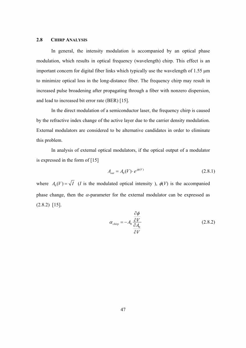
47
2.8 CHIRP ANALYSIS
In general, the intensity modulation is accompanied by an optical phase
modulation, which results in optical frequency (wavelength) chirp. This effect is an
important concern for digital fiber links which typically use the wavelength of 1.55 μm
to minimize optical loss in the long-distance fiber. The frequency chirp may result in
increased pulse broadening after propagating through a fiber with nonzero dispersion,
and lead to increased bit error rate (BER) [15].
In the direct modulation of a semiconductor laser, the frequency chirp is caused
by the refractive index change of the active layer due to the carrier density modulation.
External modulators are considered to be alternative candidates in order to eliminate
this problem.
In analysis of external optical modulators, if the optical output of a modulator
is expressed in the form of [15]
( )0 ( ) j V
outA A V e φ= ⋅ (2.8.1)
where 0 ( )A V I= (I is the modulated optical intensity ), φ(V) is the accompanied
phase change, then the α-parameter for the external modulator can be expressed as
(2.8.2) [15].
00
chirpVA AV
φ
α
∂∂= −∂∂
(2.8.2)
48
REFERENCES
[1] K. C. Gupta, “Microstrip lines and slotlines”, 2nd Ed., Artech House: Boston,
London (1996)
[2] W. Hilberg, “From approximations to exact relations for characteristic
impedances”, IEEE Trans. MTT 17, 259-265 (1969)
[3] E. Jahnke, F. Emde, and F. Lösch, “Tables of higher functions”, McGraw-Hill,
New York (1960)
[4] M. Riaziat, “Propagation modes and dispersion characteristics of coplanar
waveguides”, IEEE Trans. MTT 38, 245-251 (1990)
[5] R. E. Collin, “Foundations for microwave engineering”, 2nd Ed., McGraw-Hill
[6] David M. Pozar, “Microwave engineering”, 3rd Ed., Wiley (2005)
[7] S. Ramo, J. R. Whinnery and T. Duzer, “Fields and waves in communication
electronics”, 3rd Ed., Wiley, New York (1994)
[8] S. Adachi, “Physical properties of III-V semiconductor compounds: InP, InAs,
GaAs, GaP, InGaAs, and InGaAsP”, Wiley (1992)
[9] G. P. Agrawal and N. K. Dutta, “Semiconductor Lasers”, 2nd Ed., Van Nostrand
Reinhold, New York, (1993)
[10] B. Saleh and M. Teich, “Fundamental of photonics”, Wiley, New York (1991)
[11] S. M. Sze, “Semiconductor devices”, Wiley, New York (1985)
[12] S. M. Sze, “Physics of semiconductor devices”, 2nd Ed., Wiley, New York (1981)
[13] D. K. Schroder, “Semiconductor material and device characterization”, 3rd Ed.,
Wiley (2006)
[14] A. Yariv, “Optical electronics in modern communications”, 5th Ed. Oxford
university press, New York, Oxford (1997)
[15] K. Chang, “Handbook of optical components and engineering”, Wiley, Hoboken,
NJ (2003)
[16] S. L. Chuang, “Physics of optoelectronic devices”, Wiley, New York (1995)
[17] F. Koyama and K. IGA, “Frequency chirping in external modulators”, IEEE J.
Lightwave Technol. 6, 87-93 (1988)
49
Chapter 3
Mach-Zehnder Modulator Design
3.1 MACH-ZEHNDER INTERFEROMETER
The Mach-Zehnder interferometer (MZI) is the most popular device for
implementing optical intensity modulation using the EO effect. Modulators in this
work are also based on the concept of the MZI. Fig. 3.1 is a schematic drawing of such
an interferometer.
arm1
arm2
combinersplitter
Fig. 3.1 Schematic of a Mach-Zehnder Interferometer with 2 Y-branch
The operation of a Mach-Zehnder modulator is quite straightforward. An
incoming optical wave is split and then fed into two arms. The optical wave in each
arm can be phase modulated. The phase of the optical signal in each arm can be
manipulated independently. When the two optical signals are combined at the output,
constructive interference will occur if the relative phase between the two arms is 0°
and the output intensity will ideally be the same as that at the input. Conversely, if the
relative phase between the two arms is 180°, destructive interference will occur and the
light at the output will be completely extinguished.
Between these two extremes, the output intensity will vary in accordance with
the difference in phase between two arms.
The optical field amplitude at the output of the MZI can be generally
represented by [1]
( )1 21 2
22
j joutA A e A eφ φ= + (3.1.1)
50
where A1 and A2 represent the optical amplitudes in the two arms, and φ1 and φ2
represent the optical phase delays. The input optical power is
2 21 2inP A A= + (3.1.2)
And the output optical power is [1]
( )2 2 21 2 1 2 1 2
1 2 cos2out outP A A A A A φ φ⎡ ⎤= = + + −⎣ ⎦ (3.1.3)
The phase difference φ1 -φ2 consists of two parts: one is the phase difference φ0 at zero
applied voltage; the other is the phase difference Δφ due to the applied voltage.
Dividing Pout by the input optical power Pin, the optical intensity transfer function of
the MZI can be written in the form of [1]
( )0
1 22 2
1 2
1 1 cos2
2with
outMZI
in
PT bP
A AbA A
φ φ⎡ ⎤= = + Δ +⎣ ⎦
=+
(3.1.4)
where b is an optical imbalance factor between two arms. For an ideally balanced
symmetric design, which means 1 2A A= , 1b = and φ0=0 (3.1.4) can be simplified
as (3.1.5). The corresponding transfer curve is shown in Fig. 3.2.
[ ] 21 1 cos( ) cos2 2
φφ Δ⎛ ⎞= + Δ = ⎜ ⎟⎝ ⎠
MZIT (3.1.5)
Fig. 3.2 Transfer curve for MZI with 2 Y-branches
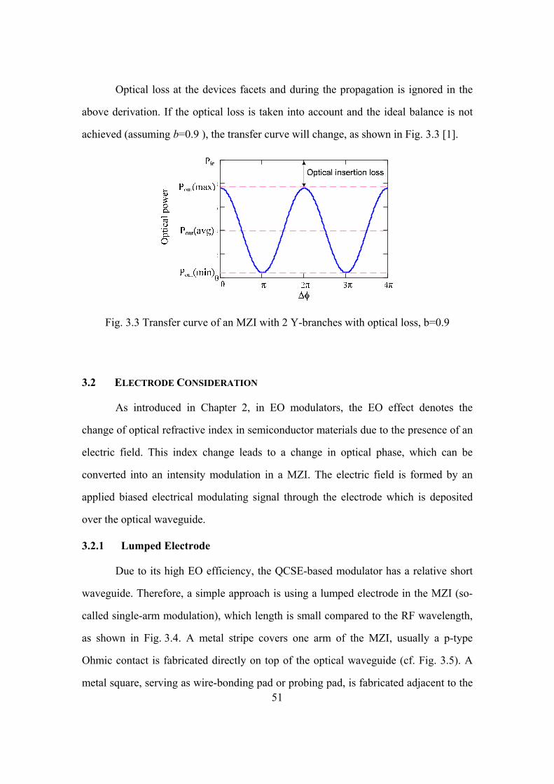
51
Optical loss at the devices facets and during the propagation is ignored in the
above derivation. If the optical loss is taken into account and the ideal balance is not
achieved (assuming b=0.9 ), the transfer curve will change, as shown in Fig. 3.3 [1].
0
2
4
6
8
Fig. 3.3 Transfer curve of an MZI with 2 Y-branches with optical loss, b=0.9
3.2 ELECTRODE CONSIDERATION
As introduced in Chapter 2, in EO modulators, the EO effect denotes the
change of optical refractive index in semiconductor materials due to the presence of an
electric field. This index change leads to a change in optical phase, which can be
converted into an intensity modulation in a MZI. The electric field is formed by an
applied biased electrical modulating signal through the electrode which is deposited
over the optical waveguide.
3.2.1 Lumped Electrode
Due to its high EO efficiency, the QCSE-based modulator has a relative short
waveguide. Therefore, a simple approach is using a lumped electrode in the MZI (so-
called single-arm modulation), which length is small compared to the RF wavelength,
as shown in Fig. 3.4. A metal stripe covers one arm of the MZI, usually a p-type
Ohmic contact is fabricated directly on top of the optical waveguide (cf. Fig. 3.5). A
metal square, serving as wire-bonding pad or probing pad, is fabricated adjacent to the
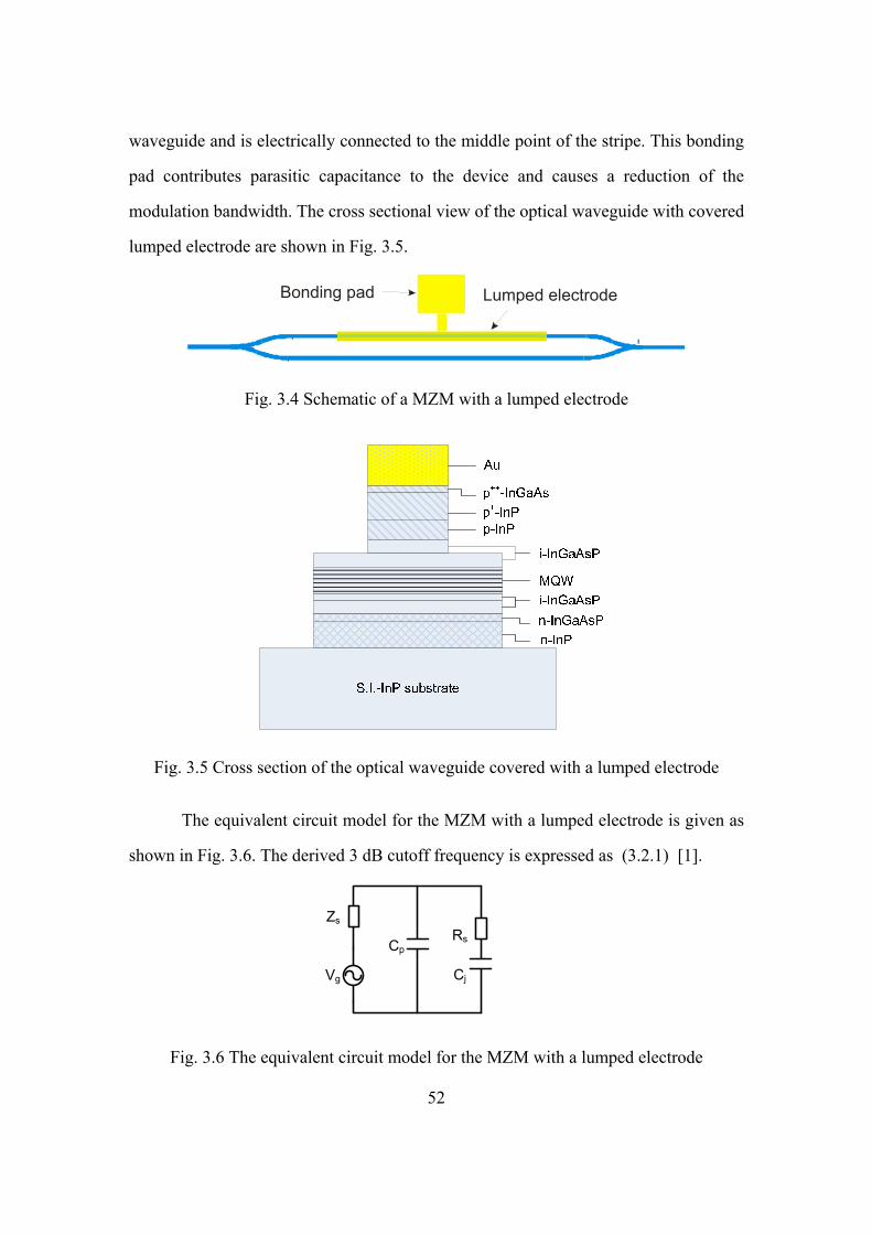
52
waveguide and is electrically connected to the middle point of the stripe. This bonding
pad contributes parasitic capacitance to the device and causes a reduction of the
modulation bandwidth. The cross sectional view of the optical waveguide with covered
lumped electrode are shown in Fig. 3.5.
Lumped electrodeBonding pad
Fig. 3.4 Schematic of a MZM with a lumped electrode
Fig. 3.5 Cross section of the optical waveguide covered with a lumped electrode
The equivalent circuit model for the MZM with a lumped electrode is given as
shown in Fig. 3.6. The derived 3 dB cutoff frequency is expressed as (3.2.1) [1].
Vg
Zs
Rs
Cj
Cp
Fig. 3.6 The equivalent circuit model for the MZM with a lumped electrode
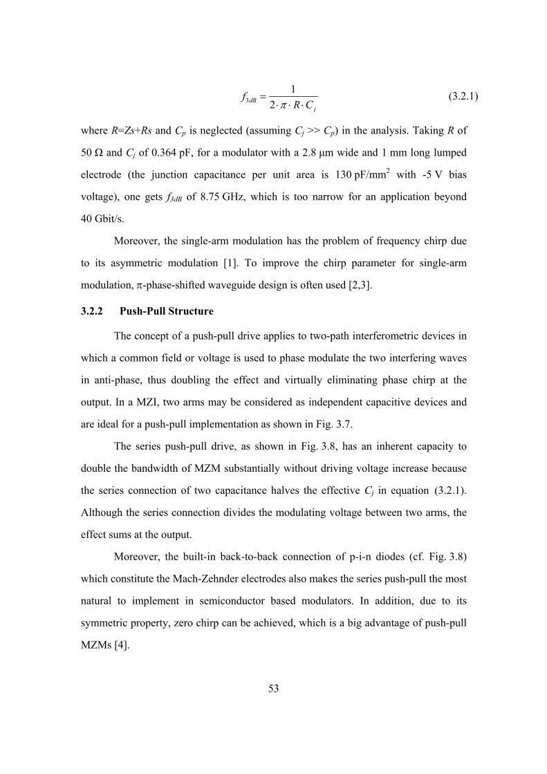
53
31
2dBj
fR Cπ
=⋅ ⋅ ⋅
(3.2.1)
where R=Zs+Rs and Cp is neglected (assuming Cj >> Cp) in the analysis. Taking R of
50 Ω and Cj of 0.364 pF, for a modulator with a 2.8 μm wide and 1 mm long lumped
electrode (the junction capacitance per unit area is 130 pF/mm2 with -5 V bias
voltage), one gets f3dB of 8.75 GHz, which is too narrow for an application beyond
40 Gbit/s.
Moreover, the single-arm modulation has the problem of frequency chirp due
to its asymmetric modulation [1]. To improve the chirp parameter for single-arm
modulation, π-phase-shifted waveguide design is often used [2,3].
3.2.2 Push-Pull Structure
The concept of a push-pull drive applies to two-path interferometric devices in
which a common field or voltage is used to phase modulate the two interfering waves
in anti-phase, thus doubling the effect and virtually eliminating phase chirp at the
output. In a MZI, two arms may be considered as independent capacitive devices and
are ideal for a push-pull implementation as shown in Fig. 3.7.
The series push-pull drive, as shown in Fig. 3.8, has an inherent capacity to
double the bandwidth of MZM substantially without driving voltage increase because
the series connection of two capacitance halves the effective Cj in equation (3.2.1).
Although the series connection divides the modulating voltage between two arms, the
effect sums at the output.
Moreover, the built-in back-to-back connection of p-i-n diodes (cf. Fig. 3.8)
which constitute the Mach-Zehnder electrodes also makes the series push-pull the most
natural to implement in semiconductor based modulators. In addition, due to its
symmetric property, zero chirp can be achieved, which is a big advantage of push-pull
MZMs [4].
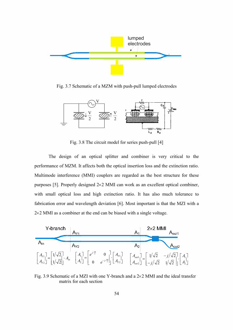
54
lumped electrodes
Fig. 3.7 Schematic of a MZM with push-pull lumped electrodes
V2
↓V2
↑
V
Fig. 3.8 The circuit model for series push-pull [4]
The design of an optical splitter and combiner is very critical to the
performance of MZM. It affects both the optical insertion loss and the extinction ratio.
Multimode interference (MMI) couplers are regarded as the best structure for these
purposes [5]. Properly designed 2×2 MMI can work as an excellent optical combiner,
with small optical loss and high extinction ratio. It has also much tolerance to
fabrication error and wavelength deviation [6]. Most important is that the MZI with a
2×2 MMI as a combiner at the end can be biased with a single voltage.
1
2
1 2
1 2Y
inY
AA
A⎡ ⎤⎡ ⎤
= ⋅⎢ ⎥⎢ ⎥⎣ ⎦ ⎢ ⎥⎣ ⎦
2
2
1 1
2 2
0
0
jY
jY
A AeA Ae
φ
φ
Δ
Δ
⋅
− ⋅
⎡ ⎤⎡ ⎤ ⎡ ⎤⎢ ⎥= ⋅⎢ ⎥ ⎢ ⎥⎢ ⎥⎣ ⎦ ⎣ ⎦⎣ ⎦
1 1
2 2
1 2 2
2 1 2out
out
A AjA Aj
⎡ ⎤−⎡ ⎤ ⎡ ⎤= ⋅⎢ ⎥⎢ ⎥ ⎢ ⎥
− ⎣ ⎦⎣ ⎦ ⎢ ⎥⎣ ⎦
Fig. 3.9 Schematic of a MZI with one Y-branch and a 2×2 MMI and the ideal transfer matrix for each section
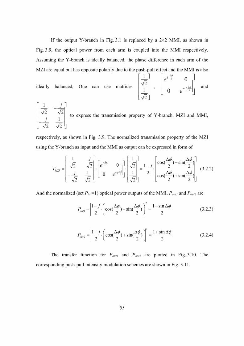
55
If the output Y-branch in Fig. 3.1 is replaced by a 2×2 MMI, as shown in
Fig. 3.9, the optical power from each arm is coupled into the MMI respectively.
Assuming the Y-branch is ideally balanced, the phase difference in each arm of the
MZI are equal but has opposite polarity due to the push-pull effect and the MMI is also
ideally balanced, One can use matrices
12
12
⎡ ⎤⎢ ⎥⎢ ⎥⎢ ⎥⎢ ⎥⎣ ⎦
,
2
2
0
0
j
j
e
e
φ
φ
Δ
Δ
⋅
− ⋅
⎡ ⎤⎢ ⎥⎢ ⎥⎣ ⎦
and
12 2
12 2
j
j
⎡ ⎤−⎢ ⎥⎢ ⎥⎢ ⎥−⎢ ⎥⎣ ⎦
to express the transmission property of Y-branch, MZI and MMI,
respectively, as shown in Fig. 3.9. The normalized transmission property of the MZI
using the Y-branch as input and the MMI as output can be expressed in form of
2
2
1 1cos( ) sin( )0 12 2 2 2 2
1 1 20 cos( ) sin( )2 22 2 2
j
MZI j
je jT
j e
φ
φ
φ φ
φ φ
Δ
Δ
⋅
− ⋅
⎡ ⎤ ⎡ ⎤ Δ Δ⎡ ⎤− −⎢ ⎥ ⎢ ⎥⎡ ⎤ ⎢ ⎥−⎢ ⎥ ⎢ ⎥⎢ ⎥= ⋅ ⋅ = ⋅ ⎢ ⎥Δ Δ⎢ ⎥ ⎢ ⎥⎢ ⎥ ⎢ ⎥⎣ ⎦− +⎢ ⎥ ⎢ ⎥ ⎢ ⎥⎣ ⎦⎣ ⎦ ⎣ ⎦
(3.2.2)
And the normalized (set Pin =1) optical power outputs of the MMI, Pout1 and Pout2 are
2
11 1 sincos( ) sin( )
2 2 2 2outjP φ φ φ− Δ Δ − Δ⎛ ⎞= ⋅ − =⎜ ⎟
⎝ ⎠ (3.2.3)
2
21 1 sincos( ) sin( )
2 2 2 2outjP φ φ φ− Δ Δ + Δ⎛ ⎞= ⋅ + =⎜ ⎟
⎝ ⎠ (3.2.4)
The transfer function for Pout1 and Pout2 are plotted in Fig. 3.10. The
corresponding push-pull intensity modulation schemes are shown in Fig. 3.11.
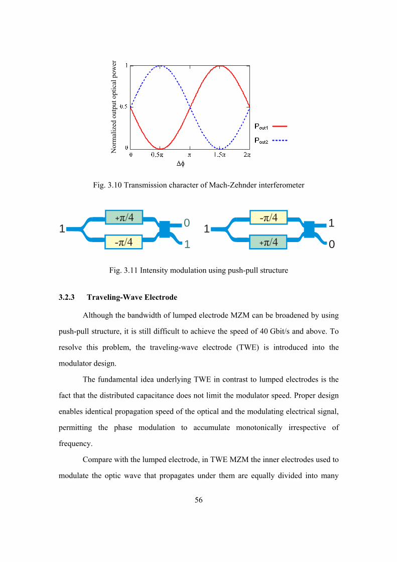
56
Nor
mal
ized
out
put o
ptic
al p
ower
Fig. 3.10 Transmission character of Mach-Zehnder interferometer
+π/4
- /4π1 0
1
- /4π
+π/41 1
0
Fig. 3.11 Intensity modulation using push-pull structure
3.2.3 Traveling-Wave Electrode
Although the bandwidth of lumped electrode MZM can be broadened by using
push-pull structure, it is still difficult to achieve the speed of 40 Gbit/s and above. To
resolve this problem, the traveling-wave electrode (TWE) is introduced into the
modulator design.
The fundamental idea underlying TWE in contrast to lumped electrodes is the
fact that the distributed capacitance does not limit the modulator speed. Proper design
enables identical propagation speed of the optical and the modulating electrical signal,
permitting the phase modulation to accumulate monotonically irrespective of
frequency.
Compare with the lumped electrode, in TWE MZM the inner electrodes used to
modulate the optic wave that propagates under them are equally divided into many
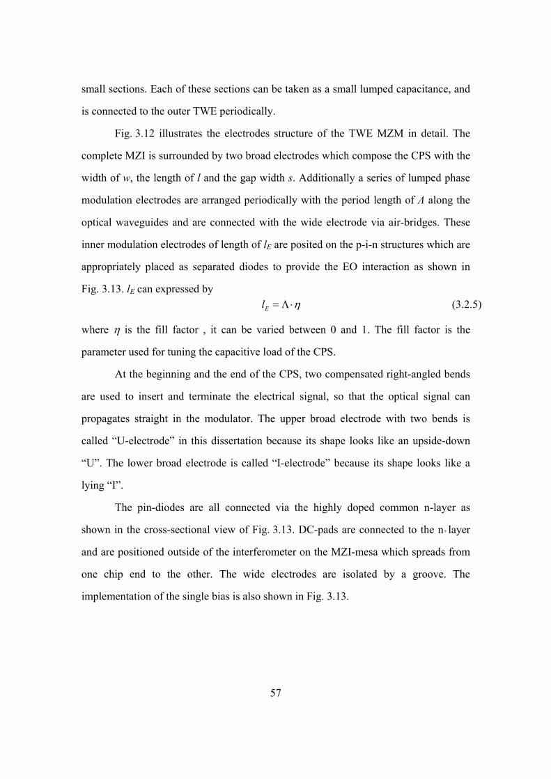
57
small sections. Each of these sections can be taken as a small lumped capacitance, and
is connected to the outer TWE periodically.
Fig. 3.12 illustrates the electrodes structure of the TWE MZM in detail. The
complete MZI is surrounded by two broad electrodes which compose the CPS with the
width of w, the length of l and the gap width s. Additionally a series of lumped phase
modulation electrodes are arranged periodically with the period length of Λ along the
optical waveguides and are connected with the wide electrode via air-bridges. These
inner modulation electrodes of length of lE are posited on the p-i-n structures which are
appropriately placed as separated diodes to provide the EO interaction as shown in
Fig. 3.13. lE can expressed by El η= Λ ⋅ (3.2.5)
where η is the fill factor , it can be varied between 0 and 1. The fill factor is the
parameter used for tuning the capacitive load of the CPS.
At the beginning and the end of the CPS, two compensated right-angled bends
are used to insert and terminate the electrical signal, so that the optical signal can
propagates straight in the modulator. The upper broad electrode with two bends is
called “U-electrode” in this dissertation because its shape looks like an upside-down
“U”. The lower broad electrode is called “I-electrode” because its shape looks like a
lying “I”.
The pin-diodes are all connected via the highly doped common n-layer as
shown in the cross-sectional view of Fig. 3.13. DC-pads are connected to the n+ layer
and are positioned outside of the interferometer on the MZI-mesa which spreads from
one chip end to the other. The wide electrodes are isolated by a groove. The
implementation of the single bias is also shown in Fig. 3.13.
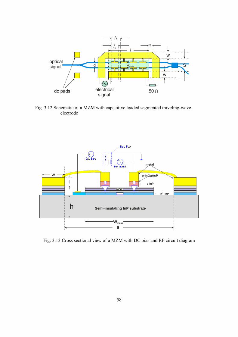
58
Λ
lE
w
w
s
s’
wmesad
l
50 Ωelectrical signal
dc pads
optical signal
Fig. 3.12 Schematic of a MZM with capacitive loaded segmented traveling-wave electrode
n+-InP
metal
MQW
p-InGaAsPw
wmesa
s
Semi-insulating InP substrate
t
h
p-InP
Fig. 3.13 Cross sectional view of a MZM with DC bias and RF circuit diagram
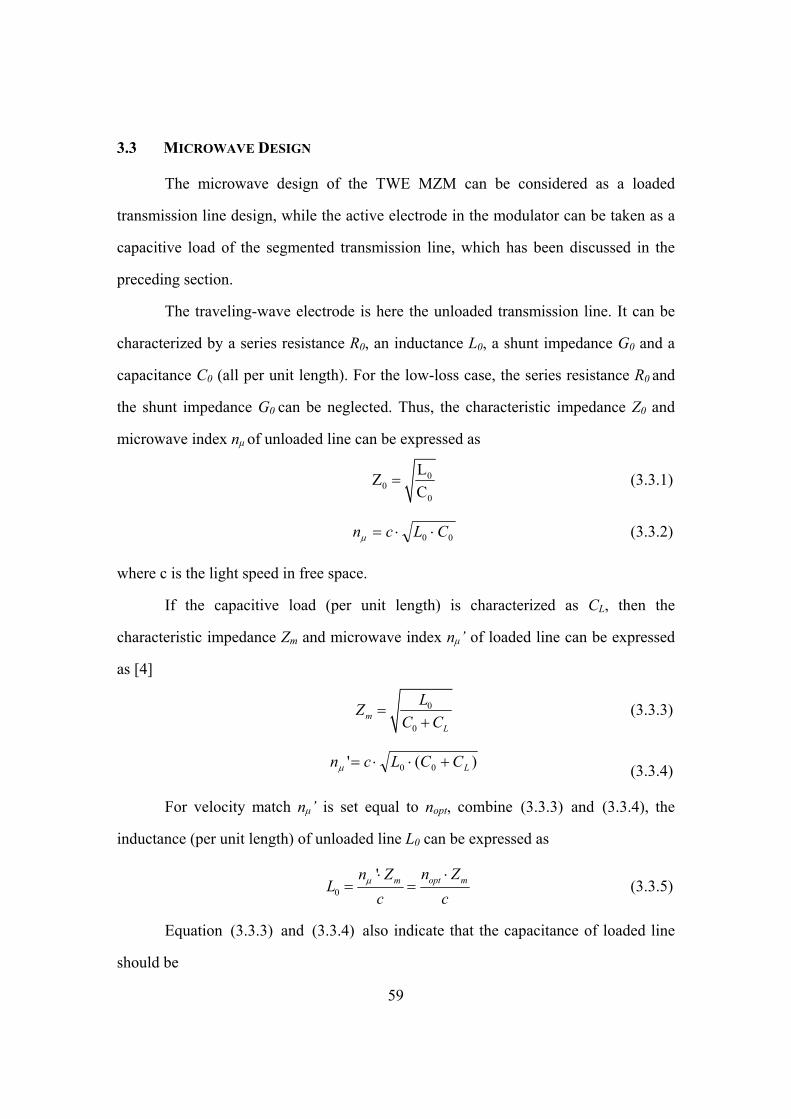
59
3.3 MICROWAVE DESIGN
The microwave design of the TWE MZM can be considered as a loaded
transmission line design, while the active electrode in the modulator can be taken as a
capacitive load of the segmented transmission line, which has been discussed in the
preceding section.
The traveling-wave electrode is here the unloaded transmission line. It can be
characterized by a series resistance R0, an inductance L0, a shunt impedance G0 and a
capacitance C0 (all per unit length). For the low-loss case, the series resistance R0 and
the shunt impedance G0 can be neglected. Thus, the characteristic impedance Z0 and
microwave index nμ of unloaded line can be expressed as
00
0
LZC
= (3.3.1)
00 CLcn ⋅⋅=μ (3.3.2)
where c is the light speed in free space.
If the capacitive load (per unit length) is characterized as CL, then the
characteristic impedance Zm and microwave index nμ’ of loaded line can be expressed
as [4]
0
0
=+m
L
LZC C
(3.3.3)
)(' 00 LCCLcn +⋅⋅=μ (3.3.4)
For velocity match nμ’ is set equal to nopt, combine (3.3.3) and (3.3.4), the
inductance (per unit length) of unloaded line L0 can be expressed as
0
'μ ⋅⋅= = opt mm n Zn Z
Lc c
(3.3.5)
Equation (3.3.3) and (3.3.4) also indicate that the capacitance of loaded line
should be
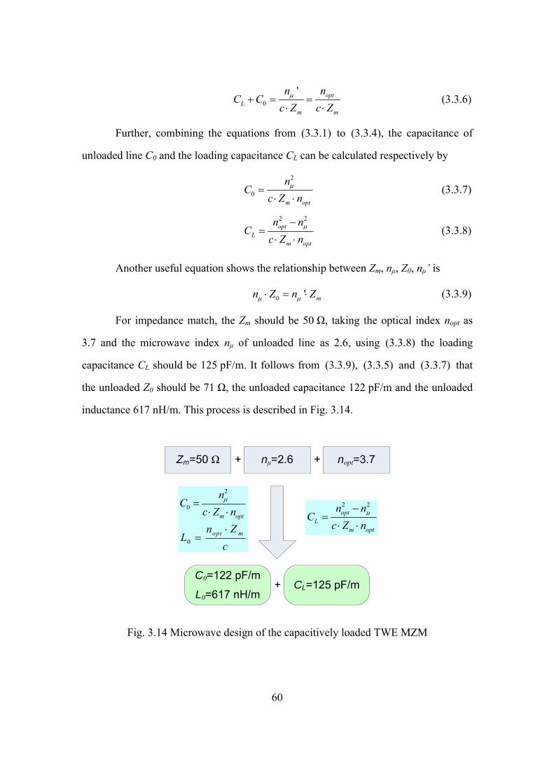
60
0
'μ+ = =⋅ ⋅
optL
m m
nnC C
c Z c Z (3.3.6)
Further, combining the equations from (3.3.1) to (3.3.4), the capacitance of
unloaded line C0 and the loading capacitance CL can be calculated respectively by
2
0μ=
⋅ ⋅m opt
nC
c Z n (3.3.7)
2 2
μ−=
⋅ ⋅opt
Lm opt
n nC
c Z n (3.3.8)
Another useful equation shows the relationship between Zm, nμ, Z0, nμ’ is
0 'μ μ⋅ = ⋅ mn Z n Z (3.3.9)
For impedance match, the Zm should be 50 Ω, taking the optical index nopt as
3.7 and the microwave index nμ of unloaded line as 2.6, using (3.3.8) the loading
capacitance CL should be 125 pF/m. It follows from (3.3.9), (3.3.5) and (3.3.7) that
the unloaded Z0 should be 71 Ω, the unloaded capacitance 122 pF/m and the unloaded
inductance 617 nH/m. This process is described in Fig. 3.14.
Zm=50 Ω nμ=2.6 nopt=3.7+ +
C0=122 pF/m
L0=617 nH/mCL=125 pF/m+
2
0μ=
⋅ ⋅m opt
nC
c Z n2 2
μ−=
⋅ ⋅opt
Lm opt
n nC
c Z n0
⋅= opt mn Z
Lc
Fig. 3.14 Microwave design of the capacitively loaded TWE MZM
61
3.4 DEFINITION OF ELECTRICAL AND ELECTRO-OPTICAL BANDWIDTH
Bandwidth is one of those important factors which characterize the quality of a
modulator.
The electro-optic bandwidth of a TWE MZM is defined as the frequency, for
which the optical intensity modulation depth has fallen to 70.7% of the reference level,
causing a 3 dB reduction in the received signal [4].
In electro-optic modulators, the amount of phase shift experienced by a photon
from entering to exiting the waveguide is directly proportional to the voltage applied
across the waveguide with the constant of proportionality containing parameters such
as the waveguide dimensions, optical wavelength, index of refraction, overlap between
the optical wave and the microwave, and the electro-optic coefficient. Since the
applied voltage is of traveling-wave nature, the total amount of phase shift attained by
a photon is cumulative of all phase shifts induced by the instantaneous voltage seen by
the photon at a particular position on the line.
Fig. 3.15 shows a simplified equivalent circuit for a traveling-wave electrode
modulator. In this model, the whole modulator is treated electrically as a transmission
line.
Fig. 3.15 Equivalent circuit of a traveling-wave electrode modulator
In this model, the modulating voltage at position x is given as [7,8]
( ) ( )
21
1 2
( , ) (1 )2
opt optopt
j x j xj lg
m l l
V e eV x ee e
γ β γ ββ
γ γ
ρω ρρ ρ
− ⋅ − − ⋅⋅ ⋅
⋅ − ⋅
+ ⋅= ⋅ + ⋅ ⋅
+ ⋅ ⋅ (3.4.1)
62
where
sm
sm
ZZZZ
+−
=1ρ (3.4.1a)
mT
mT
ZZZZ
+−
=2ρ (3.4.1b)
optm
opt nc
⋅=ω
β (3.4.1c)
j μγ α β= + (3.4.1d)
m ncμ μ
ωβ = ⋅ (3.4.1e)
The physical meaning of the variables in (3.4.1) is defined as follow Vg is the amplitude of the driving voltage, ωm is the modulation frequency, l is the traveling-wave electrode length, ρ1 is the input electrode structure reflection coefficient, ρ2 is the output electrode structure reflection coefficient, Zm is the characteristic impedance of the modulator, ZS is the source impedance, normally is 50 Ω, ZT is the terminating impedance , γ is the complex microwave transmission constant, α is the microwave attenuation constant, βμ is the microwave propagation constant of the signal in the electrode, βopt is the optical propagation constant of the signal in the optical waveguide, nμ is the microwave refractive index, nopt is the optical refractive index, c is the velocity of light in vacuum.
While under small signal modulation, the modulation depth is proportional to
the modulating voltage, the modulation reduction factor r(x,ωm) can be defined as
)0,(
),(),(lV
xVxr mm
ωω = (3.4.2)
As defined earlier, the electro-optic bandwidth of TWE MZM is the frequency, for
which the optical intensity modulation reduction factor has fallen to 70.7% of the
reference level. This can be expressed as
63
2
1)( =mr ω (3.4.3)
To simplify the analysis, the average voltage Vavg(ωm) can be used instead of
V(x, ωm), the modulation reduction factor can be simplified as [9]
)0()(
)(avg
mavgm V
Vr
ωω = (3.4.4)
here Vavg(ωm) is the average voltage along a length of l. It can be expressed as [7,8]:
1
201 2
(1 )1( ) ( , ) ( )2 ( )
optj ll g
avg m m l l
V eV V x dx V V
l e e
β
γ γ
ρω ω ρ
ρ ρ
⋅ ⋅
+ −⋅ − ⋅
⋅ + ⋅= ⋅ = ⋅ + ⋅
⋅ + ⋅ ⋅∫ (3.4.5)
where
±
±⋅±± ⋅= ±
φφφ sinjeV (3.4.5a)
( )2
optj lγ βφ±
− ⋅ ⋅=
∓ (3.4.5b)
V+ is the single pass average voltage experienced by a photon due to the forward traveling sinusoidal voltage, V- is the single pass average voltage experienced by a photon due to the reverse traveling sinusoidal voltage,
+φ is the complex phase differential between the microwave and optical signals for a forward traveling sinusoidal voltage after propagating the length of the electrode
−φ is the complex phase differential between the microwave and optical signals for a reverse traveling sinusoidal voltage after propagating the length of the electrode.
Inserting (3.4.5) into (3.4.4), we get
1 2 2
2 1 2
1( )1m l l
V Vre eγ γ
ρ ρ ρωρ ρ ρ
+ −⋅ − ⋅
− ⋅ + ⋅= ⋅
+ − ⋅ ⋅ (3.4.6)
Note that, in this equation, the impedance mismatch, microwave loss and the
velocity mismatch are all taken into consideration.

64
Perfect impedance match
For a perfectly matched line, that is Zm = ZS = ZT = 50 Ω, ρ1 and ρ2 are zero,
which reduce (3.4.6) to the familiar expression of
+
+⋅−
⋅=φ
φωα sin)( 2
l
m er (3.4.7)
( ) ( )( )
2 2 2opt m optm
opt
j l f l n nl ln n j jc c
μμ
γ β πω αφ α+
− ⋅ − ⋅ ⋅ ⋅ ⋅ − ⋅⎡ ⎤= = ⋅ − − ⋅ = − ⋅⎢ ⎥⎣ ⎦ (3.4.7a)
Perfect impedance match + lossless
Further, if there is no microwave loss, that is α=0, we get from (3.4.7)
Δ
Δ==
+
+ sinsin)(φ
φωmr (3.4.8)
c
nnlf optm )( −⋅⋅⋅=Δ μπ
(3.4.8a)
Inserting (3.4.8) into (3.4.3), we get the electro-optic bandwidth
31.39( )eodB
opt
cfl n nμπ
⋅=
⋅ ⋅ − (3.4.9)
This equation is well known as expressing the relationship between the
bandwidth and the velocity mismatch. It is notable that this relationship is based on the
premise that the device has a characteristic impedance of 50 Ω and the microwave loss
of the whole device is neglected.
Perfect impedance match + Perfect velocity match
If the velocities of microwave and optical wave have been perfectly matched, that is μnnopt = , we get from (3.4.7)
2
)2
sin()( 2
lj
lj
erl
m ⋅⋅−
⋅⋅−
⋅=⋅−
α
α
ωα
(3.4.10)
65
Using Euler’s formula (see details in appendix B), (3.4.10) can be rewritten as
l
erl
m ⋅−
=⋅−
αω
α1)( (3.4.11)
Inserting (3.4.11) into (3.4.3), we get that at the frequency, for which the
optical intensity modulation depth has fallen to 70.7% of the reference level
7384.0=⋅ lα (3.4.12) And under this condition the electrical loss is [10]
0.738420 log 20 log( ) 20 log( ) 6.4 dBl le e eγ α− ⋅ − ⋅ −⋅ = ⋅ = ⋅ = − (3.4.13)
Under the condition that the velocity and the impedance are perfectly matched,
we can determine the electro-optic 3 dB bandwidth by measuring the electrical loss,
i.e. S21. The frequency, for which the electrical loss of the whole modulator has fallen
to -6.4 dB, can be taken as the 3 dB cut-off frequency of the electro-optical response.
Velocity mismatch + Partly impedance match+ Microwave loss
Actually in a modulator the microwave loss and the velocity mismatch can be
optimised but cannot be completely avoided. Consequently, it is necessary to analyse
the frequency response of the modulator with both microwave loss and velocity
mismatch. Another interesting thing in (3.4.6) is that, if ρ1 and ρ2 cannot
simultaneously equal to zero, but if we can make ρ2 equal to zero, that is Zm = ZT ,
(3.4.7) is still valid. This condition is not so strict as the perfect impedance match, it
can be done by terminating the modulator with a proper impedance, which is called
“partly impedance match”.
The (3.4.7) can be used here, further analysis shows that [10]
22
2
2)(
22
)()(
1)cos(2)(
1sinsin)(ll
leee
ljeeer
opt
optlll
j
opt
ljll
m
optopt
⋅+⋅
+⋅⋅⋅−=⋅
⋅⋅+−
=⋅=⋅=⋅−⋅⋅−⋅
⋅⋅⋅+−
+
+⋅−
+
+⋅−
μ
μααβ
μ
βααα
βα
ββαφ
φφ
φωμμ
(3.4.14)
with )( optm
opt nnc
−= μμ ωβ (3.4.14a)
66
From (3.4.14), one can see that, to determine r(ωm), α⋅l and lopt ⋅μβ should be
known. As defined in (3.4.1), l is the TWE length; α is the microwave attenuation
constant, this parameter characterizes the microwave loss of the whole device and is a
function of frequency; μβopt is defined in (3.4.14a), it characterizes the velocity
mismatch in the modulator. The calculation of nμ and nopt will be introduced in detail in
Chapter 4.
In a TWE MZM, one can take the whole electrodes including outer electrodes
and periodic capacitive loading with reverse bias voltage as a transmission line. Using
the transmission line model, which has been explained in Chapter 2, the microwave
loss coefficient of a modulator, α, is the attenuation constant of the transmission line,
consequently, combined with the scattering matrix of transmission line, α can be
expressed as
21)exp( Sl =⋅−α (3.4.15)
Inserting (3.4.15) into (3.4.14), it can be rewritten as
22
21
212
21
)()(ln
1)cos(2)(
lS
lSSr
opt
optm
⋅+
+⋅⋅⋅−=
μ
μ
β
βω (3.4.16)
Since the scattering matrix can be obtained either in an EM simulation tool or
by direct measurement using a network analyser, (3.4.16) is very useful both in
design and in measurement to predict the electro-optic bandwidth of the TWE MZM.
3.5 DRIVING VOLTAGE VΠ
The driving voltage, Vπ , also called the half wave voltage or the switching
voltage, is a very important parameter for an MZM. It is the voltage value at which the
voltage-induced phase difference reaches π (or 180°) in an MZM.
67
The phase difference φ1-φ2 in a MZM consists of two parts: one is the phase
difference Φ0 at zero applied voltage and the other is the phase difference Δφ due to the
applied voltage. If only one arm is modulated, the phase difference is [1]
2( ) ( ) effV n V lπφ γλ
Δ = ⋅Δ ⋅ ⋅ (3.5.1)
where Δn(V) is the optical index change in the waveguide active layer; γ is the optical
confinement factor, defined as the portion of optical mode that is confined in the active
layer, leff is the effective modulation length and is defined by
effl l η= ⋅ (3.5.2)
If the modulation is based on the LEO effect, Δn(V) can be described as [1]
30 41
1( )2 pin
Vn V n rd
Δ = ⋅ ⋅ ⋅ (3.5.3)
where n0 is the optical index of the active layer at zero applied voltage; r41 is the
relevant InP EO coefficient, V is the voltage applied vertically across the optical
waveguide, dpin is the depletion layer width of a reverse biased p-i-n junction.
Combining (3.5.1) and (3.5.3), one gets
30( ) eff
ijpin
lV n r V
dγπφ
λ⋅
Δ = ⋅ ⋅ ⋅ ⋅ (3.5.4)
and
30
pin
ij eff
dV
n r lπλ
γ= ⋅
⋅ ⋅ (3.5.5)
For MZMs using the QCSE, the relationship between Δn and V is nonlinear,
but Δn is proportional to V, therefore (3.5.5) can be rewritten as
30
pin
ij eff
dV
n r lπλ
γ∝ ⋅
⋅ ⋅ (3.5.6)
68
REFERENCES
[1] K. Chang, “Handbook of optical components and engineering”, Wiley, Hoboken, NJ (2003)
[2] J. Yu, C. Rolland, D. Yevick, A. Somani, and S. Bradshaw, “A novel method for improving the performance of InP/InGaAsP multiple-quantum-well Mach–Zehnder modulators by phase shift engineering”, Proc. IPRM’96 (Int. Conf. InP and Related Materials), paper 1TuG4-1, 376-379 (1996)
[3] D. Penninckx and Ph. Delansay, “Comparison of the propagation performance over standard dispersive fiber between InP-based π-phase-shifted and symmetrical Mach-Zehnder modulators,” IEEE Photon. Technol. Lett., 9, 1250-1252 (1997)
[4] R. G. Walker: “High-Speed III-V Semiconductor Intensity Modulators,” IEEE J. Quantum Electron. 27, 654-667 (1991)
[5] L. B. Soldano and E. C. M. Pennings, “Optical multi-mode interference devices based on self-imaging: principles and applications”, J. Lightwave Technol., 13, 615-627 (1995)
[6] C. Rolland, R. S. Moore, F. Shepherd, and G. Hillier, “10 Gbit/s, 1.56 μm multiquantum well InP/InGaAsP Mach-Zehnder optical modulator,” Electron. Lett. 29, 471-472 (1993)
[7] S. H. Lin and S. Y. Wang, “High throughput GaAs p-i-n electrooptic modulator with a 3dB bandwidth of 9.6 GHz at 1.3 μm,” Appl. Opt. 26, 1696-1700 (1987)
[8] S. Y. Wang and S. H. Lin, “High speed III-V electrooptic waveguide modulators at λ=1.3 μm,” IEEE J. Lightwave Technol. 6, 758-771 (1988)
[9] I. Kim, M. R. T. Tan and S. Y.Wang, “Analysis of a new microwave low-loss and velocity-matched III-V transmission line for traveling-wave electrooptic modulators,” IEEE J. Lightwave Technol. 8 ,728-738 (1990)
[10] E. Voges and K. Petermann, “Optische kommunikationstechnik”, Springer, Berlin (2002)
69
Chapter 4
Optimization towards Higher Speed and Lower Driving Voltage
The driving voltage and the 3 dBeo bandwidth are two important parameters for
external modulators. It is difficult to achieve both parameters to their optimum. There
is some trade-off during the optimization. For example, the 3 dBeo bandwidth and the
driving voltage are inversely proportional to the effective modulation length and
proportional to the i-region thickness when the device speed is limited by sample
capacitance. In this Chapter, the simulation methods, tools and three different models
as well as optimization strategies towards a low driving voltage 80 Gbit/s modulator
will be discussed concretely.
4.1 ELECTROMAGNETIC SIMULATION
The electromagnetic simulation plays an important role in modulator electrode
design. Highly accurate design data are necessary for these devices because of the long
and costly fabrication process. Hence a rigorous model is needed that includes the
main limiting factors: the velocity mismatch between the optical wave and the
microwave as well as the microwave loss.
4.1.1 Introduction of High Frequency Structure Simulator
The high frequency structure simulator (HFSS) from Ansoft®, as an industry-
standard software for S-parameter and full-wave SPICE extraction and for the
electromagnetic simulation of high-frequency and high-speed components, is a high-
performance full-wave electromagnetic (EM) field simulator for arbitrary three
dimensional (3-D) volumetric passive device modeling. It integrates simulation,
visualization, solid modeling, and automation in an environment where solutions to the
3-D EM problems are accurately obtained. All of the EM simulations involved in this
work were carried out in HFSS (either in HFSS version9 or in HFSS version10).
70
HFSS employs the finite element method (FEM) and adaptive meshing to give
an insight to the 3-D EM problems. The FEM originated as a method for modeling
stress in structural mechanics applications, but was adapted to electromagnetics in the
1970s. Today, the FEM as a numerical method is well known in the electromagnetics
and microwaves community, it can solve electromagnetic fields in structures with
arbitrary boundary shape.
The FEM involves subdividing a large problem into individually simple
constituent units which are each solvable via direct analytical methods, then
reassembling the solution for the entire problem space as a matrix of simultaneous
equations. In HFSS, the finite subsection (finite elements) over which they are defined,
are contiguous and of the simplest possible shape. For an arbitrary 3-D problem they
are tetrahedral volume elements. In HFSS, the mesh is the mapping of tetrahedral
elements to the 3-D geometry for which a solution is desired.
Fig. 4.1 [1] shows the flow chart of the general design process of HFSS. The
complete arbitrary 3-D geometry with material properties should be defined as the
input for an EM simulation. In addition, boundary conditions specify the field behavior
at the edges of the problem region and object interfaces.
To ensure an accurate simulation result as well as an acceptable calculation
time, the solution criteria should be defined carefully. The more rigorous the criteria
are, the more accurate results will be calculated. However, a considerable quantity of
matrices will also be generated to fulfill the criteria due to the sharp increasing number
of tetrahedra. This will directly lead to enormous calculations and an unacceptable
calculating time, sometimes the relevant calculation can even exceed the capability of
the calculating computer.
A normal simulation starts from generating the initial meshing data with
respect to the electrical solution wavelength, the so-called lambda refinement results in
tetrahedra of about λ/4 in free space as the starting value. HFSS solves field equations
derived from Maxwell’s equations on the existing mesh. However, for many field
71
behaviors this may not be sufficient mesh density to properly solve for rapid
fluctuations or extremely localized effects. Hence an adaptive refinement is followed.
HFSS estimates the error in each element in the mesh, and refines those elements
having the highest errors till the stopping criteria are met (cf. Fig. 4.2). The maximum
delta-S is a frequently used convergence criterion. The delta-S is the magnitude of the
change of the S-parameters between two consecutive passes. The value set for
maximum delta-S is a stopping criterion for the adaptive solution. If the magnitude of
the change of all S-parameters is less than this value from one iteration to the next, the
adaptive analysis stops. Otherwise, it continues until the requested number of passes is
completed. Here, the number of passes is a useful criterion to prevent the size of
matrix used for the calculation exceeding the hardware limit. These two criteria are
always used together in HFSS.
After the adaptive refinement, HFSS will use the established mesh data to solve
the problem for the whole frequency range that has been defined by the designer. The
frequency sweeping method used in the simulation can be chosen from one of three
types, namely, discrete sweep, fast sweep or interpolating sweep.
Finally, the simulation results including EM fields and S-parameters as well as
Y-matrices and Z-matrices could be plotted or expressed in tables or curves.
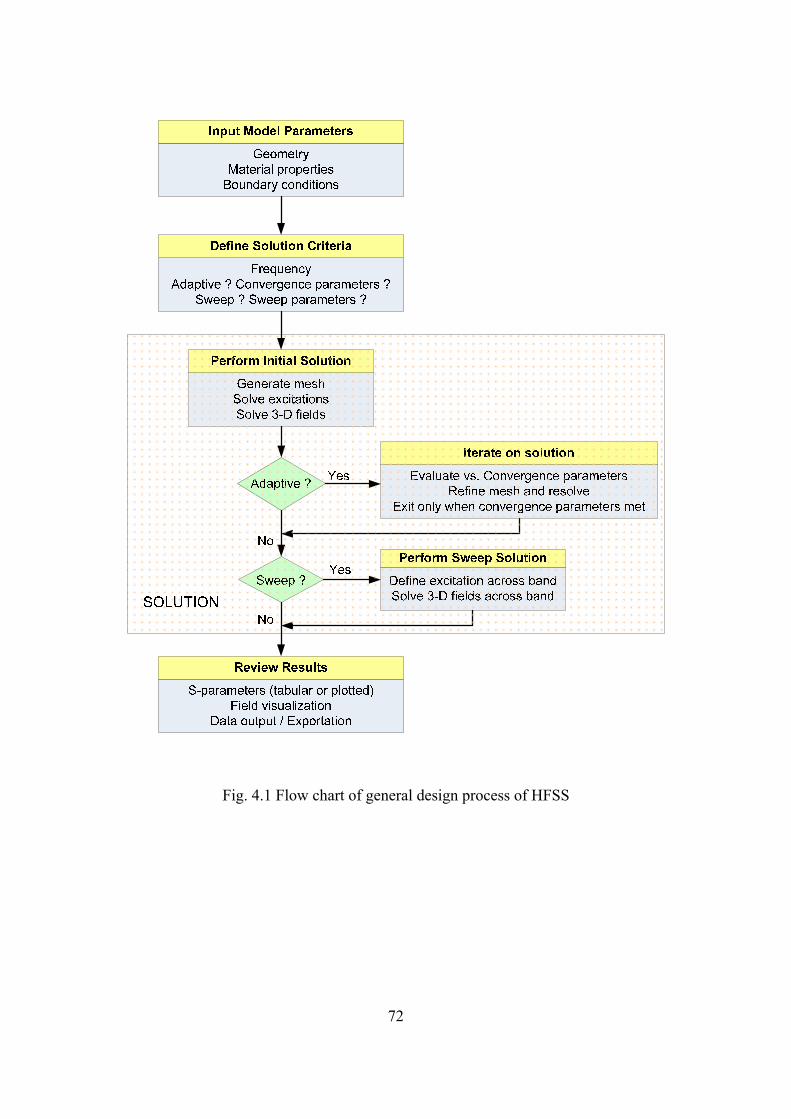
72
Fig. 4.1 Flow chart of general design process of HFSS
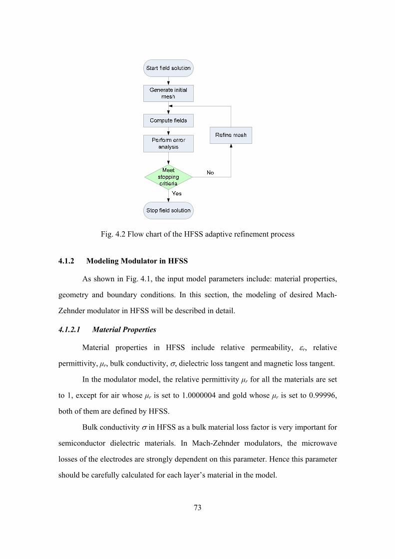
73
Fig. 4.2 Flow chart of the HFSS adaptive refinement process
4.1.2 Modeling Modulator in HFSS
As shown in Fig. 4.1, the input model parameters include: material properties,
geometry and boundary conditions. In this section, the modeling of desired Mach-
Zehnder modulator in HFSS will be described in detail.
4.1.2.1 Material Properties
Material properties in HFSS include relative permeability, εr, relative
permittivity, μr, bulk conductivity, σ, dielectric loss tangent and magnetic loss tangent.
In the modulator model, the relative permittivity μr for all the materials are set
to 1, except for air whose μr is set to 1.0000004 and gold whose μr is set to 0.99996,
both of them are defined by HFSS.
Bulk conductivity σ in HFSS as a bulk material loss factor is very important for
semiconductor dielectric materials. In Mach-Zehnder modulators, the microwave
losses of the electrodes are strongly dependent on this parameter. Hence this parameter
should be carefully calculated for each layer’s material in the model.
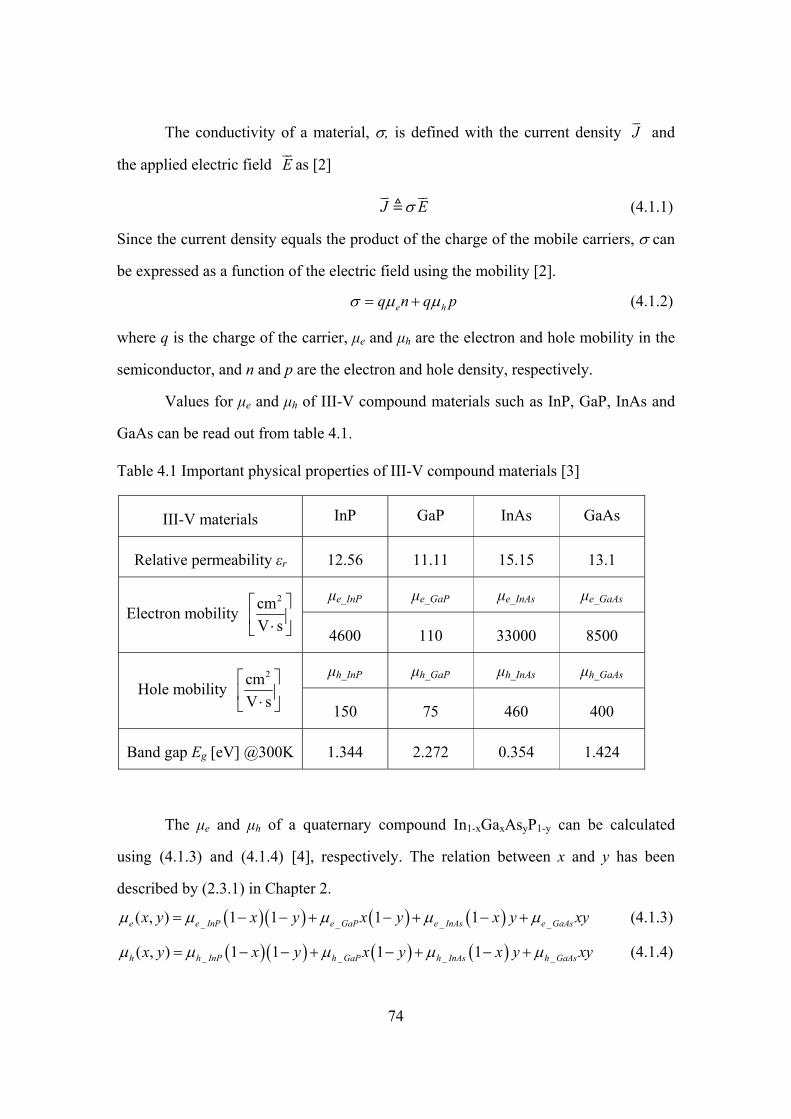
74
The conductivity of a material, σ, is defined with the current density J and
the applied electric field E as [2]
J Eσ (4.1.1)
Since the current density equals the product of the charge of the mobile carriers, σ can
be expressed as a function of the electric field using the mobility [2].
e hq n q pσ μ μ= + (4.1.2)
where q is the charge of the carrier, μe and μh are the electron and hole mobility in the
semiconductor, and n and p are the electron and hole density, respectively.
Values for μe and μh of III-V compound materials such as InP, GaP, InAs and
GaAs can be read out from table 4.1.
Table 4.1 Important physical properties of III-V compound materials [3]
III-V materials InP GaP InAs GaAs
Relative permeability εr 12.56 11.11 15.15 13.1
μe_InP μe_GaP μe_InAs μe_GaAs Electron mobility
2cmV s
⎡ ⎤⎢ ⎥⋅⎣ ⎦
4600 110 33000 8500
μh_InP μh_GaP μh_InAs μh_GaAs Hole mobility
2cmV s
⎡ ⎤⎢ ⎥⋅⎣ ⎦
150 75 460 400
Band gap Eg [eV] @300K 1.344 2.272 0.354 1.424
The μe and μh of a quaternary compound In1-xGaxAsyP1-y can be calculated
using (4.1.3) and (4.1.4) [4], respectively. The relation between x and y has been
described by (2.3.1) in Chapter 2.
( )( ) ( ) ( )_ _ _ _( , ) 1 1 1 1e e InP e GaP e InAs e GaAsx y x y x y x y xyμ μ μ μ μ= − − + − + − + (4.1.3)
( )( ) ( ) ( )_ _ _ _( , ) 1 1 1 1h h InP h GaP h InAs h GaAsx y x y x y x y xyμ μ μ μ μ= − − + − + − + (4.1.4)
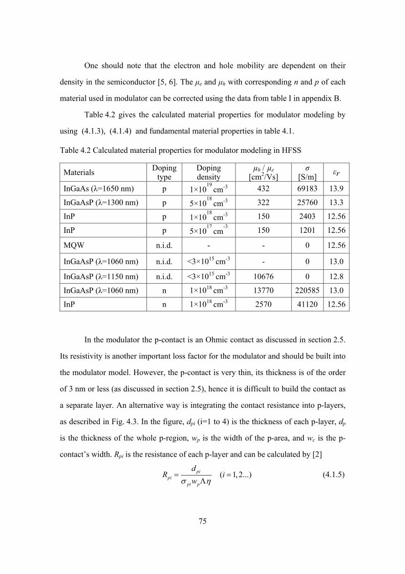
75
One should note that the electron and hole mobility are dependent on their
density in the semiconductor [5, 6]. The μe and μh with corresponding n and p of each
material used in modulator can be corrected using the data from table I in appendix B.
Table 4.2 gives the calculated material properties for modulator modeling by
using (4.1.3), (4.1.4) and fundamental material properties in table 4.1.
Table 4.2 Calculated material properties for modulator modeling in HFSS
Materials Doping type
Doping density
µh / µe [cm2/Vs]
σ [S/m] εr
InGaAs (λ=1650 nm) p 1×10¹⁹
cm-3 432 69183 13.9
InGaAsP (λ=1300 nm) p 5×10¹⁸
cm-3 322 25760 13.3
InP p 1×10¹⁸
cm-3 150 2403 12.56
InP p 5×10¹⁷
cm-3
150 1201 12.56
MQW n.i.d. - - 0 12.56
InGaAsP (λ=1060 nm) n.i.d. <3×1015 cm-3 - 0 13.0
InGaAsP (λ=1150 nm) n.i.d. <3×1015 cm-3 10676 0 12.8
InGaAsP (λ=1060 nm) n 1×1018 cm-3 13770 220585 13.0
InP n 1×1018 cm-3 2570 41120 12.56
In the modulator the p-contact is an Ohmic contact as discussed in section 2.5.
Its resistivity is another important loss factor for the modulator and should be built into
the modulator model. However, the p-contact is very thin, its thickness is of the order
of 3 nm or less (as discussed in section 2.5), hence it is difficult to build the contact as
a separate layer. An alternative way is integrating the contact resistance into p-layers,
as described in Fig. 4.3. In the figure, dpi (i=1 to 4) is the thickness of each p-layer, dp
is the thickness of the whole p-region, wp is the width of the p-area, and wc is the p-
contact’s width. Rpi is the resistance of each p-layer and can be calculated by [2]
( 1, 2...)pipi
pi p
dR i
wσ η= =
Λ (4.1.5)
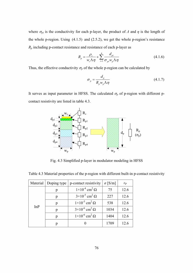
76
where σpi is the conductivity for each p-layer, the product of Λ and η is the length of
the whole p-region. Using (4.1.5) and (2.5.2), we get the whole p-region’s resistance
Rp including p-contact resistance and resistance of each p-layer as
4
1
picp
ic pi p
dR
w wρ
η σ η=
= +Λ Λ∑ (4.1.6)
Thus, the effective conductivity σp of the whole p-region can be calculated by
pp
p p
dR w
ση
=Λ
(4.1.7)
It serves as input parameter in HFSS. The calculated σp of p-region with different p-
contact resistivity are listed in table 4.3.
Rc
Rp1
Rp2
Rp3
Rp4
Rp (σp)
dp4
dp3
dp2
dp1
dp
wpwp
wc
Fig. 4.3 Simplified p-layer in modulator modeling in HFSS
Table 4.3 Material properties of the p-region with different built-in p-contact resistivity
Material Doping type p-contact resistivity σ [S/m] εr
p 1×10⁻⁴ cm2·Ω 75 12.6
p 3×10⁻⁵ cm2·Ω 227 12.6
p 1×10⁻⁵ cm2·Ω 538 12.6
p 3×10⁻⁶ cm2·Ω 1034 12.6
p 1×10⁻⁶ cm2·Ω 1404 12.6
InP
p 0 1709 12.6
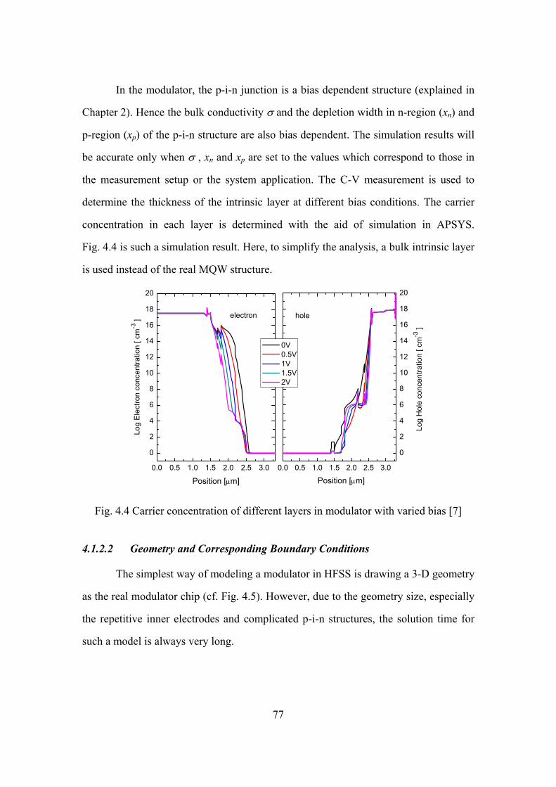
77
In the modulator, the p-i-n junction is a bias dependent structure (explained in
Chapter 2). Hence the bulk conductivity σ and the depletion width in n-region (xn) and
p-region (xp) of the p-i-n structure are also bias dependent. The simulation results will
be accurate only when σ , xn and xp are set to the values which correspond to those in
the measurement setup or the system application. The C-V measurement is used to
determine the thickness of the intrinsic layer at different bias conditions. The carrier
concentration in each layer is determined with the aid of simulation in APSYS.
Fig. 4.4 is such a simulation result. Here, to simplify the analysis, a bulk intrinsic layer
is used instead of the real MQW structure.
0.0 0.5 1.0 1.5 2.0 2.5 3.0
0
2
4
6
8
10
12
14
16
18
20
0.0 0.5 1.0 1.5 2.0 2.5 3.0
0
2
4
6
8
10
12
14
16
18
20
Position [μm]
Log
Hol
e co
ncen
tratio
n [ c
m-3
]
Log
Ele
ctro
n co
ncen
tratio
n [ c
m-3
]
Position [μm]
0V 0.5V 1V 1.5V 2V
electron
hole
Fig. 4.4 Carrier concentration of different layers in modulator with varied bias [7]
4.1.2.2 Geometry and Corresponding Boundary Conditions
The simplest way of modeling a modulator in HFSS is drawing a 3-D geometry
as the real modulator chip (cf. Fig. 4.5). However, due to the geometry size, especially
the repetitive inner electrodes and complicated p-i-n structures, the solution time for
such a model is always very long.
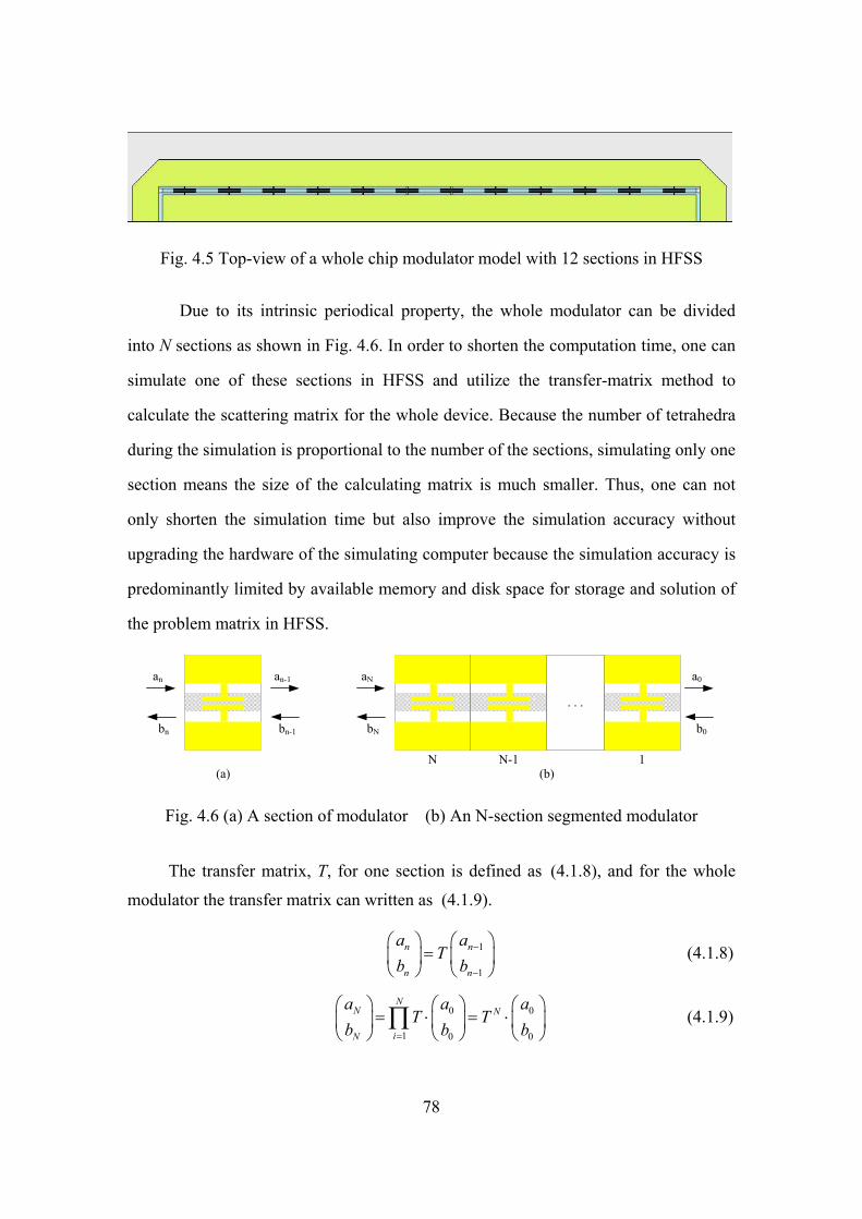
78
Fig. 4.5 Top-view of a whole chip modulator model with 12 sections in HFSS
Due to its intrinsic periodical property, the whole modulator can be divided
into N sections as shown in Fig. 4.6. In order to shorten the computation time, one can
simulate one of these sections in HFSS and utilize the transfer-matrix method to
calculate the scattering matrix for the whole device. Because the number of tetrahedra
during the simulation is proportional to the number of the sections, simulating only one
section means the size of the calculating matrix is much smaller. Thus, one can not
only shorten the simulation time but also improve the simulation accuracy without
upgrading the hardware of the simulating computer because the simulation accuracy is
predominantly limited by available memory and disk space for storage and solution of
the problem matrix in HFSS.
a0
b0
aN
bN
. . .
N N-1 1
an-1
bn-1
an
bn
(a) (b)
Fig. 4.6 (a) A section of modulator (b) An N-section segmented modulator
The transfer matrix, T, for one section is defined as (4.1.8), and for the whole
modulator the transfer matrix can written as (4.1.9).
1
1
n n
n n
a aT
b b−
−
⎛ ⎞ ⎛ ⎞=⎜ ⎟ ⎜ ⎟
⎝ ⎠ ⎝ ⎠ (4.1.8)
0 0
1 0 0
NN N
iN
a a aT T
b b b=
⎛ ⎞ ⎛ ⎞ ⎛ ⎞= ⋅ = ⋅⎜ ⎟ ⎜ ⎟ ⎜ ⎟
⎝ ⎠ ⎝ ⎠ ⎝ ⎠∏ (4.1.9)
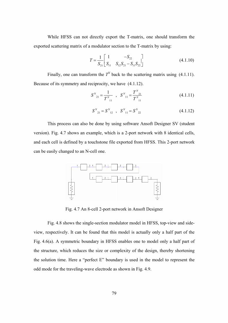
79
While HFSS can not directly export the T-matrix, one should transform the
exported scattering matrix of a modulator section to the T-matrix by using:
22
11 12 21 11 2221
11 ST
S S S S SS−⎡ ⎤
= ⎢ ⎥−⎣ ⎦ (4.1.10)
Finally, one can transform the TN back to the scattering matrix using (4.1.11).
Because of its symmetry and reciprocity, we have (4.1.12).
2121 11
11 11
1 , N
N NN N
TS ST T
= = (4.1.11)
21 12 11 22 , N N N NS S S S= = (4.1.12)
This process can also be done by using software Ansoft Designer SV (student
version). Fig. 4.7 shows an example, which is a 2-port network with 8 identical cells,
and each cell is defined by a touchstone file exported from HFSS. This 2-port network
can be easily changed to an N-cell one.
Fig. 4.7 An 8-cell 2-port network in Ansoft Designer
Fig. 4.8 shows the single-section modulator model in HFSS, top-view and side-
view, respectively. It can be found that this model is actually only a half part of the
Fig. 4.6(a). A symmetric boundary in HFSS enables one to model only a half part of
the structure, which reduces the size or complexity of the design, thereby shortening
the solution time. Here a “perfect E” boundary is used in the model to represent the
odd mode for the traveling-wave electrode as shown in Fig. 4.9.
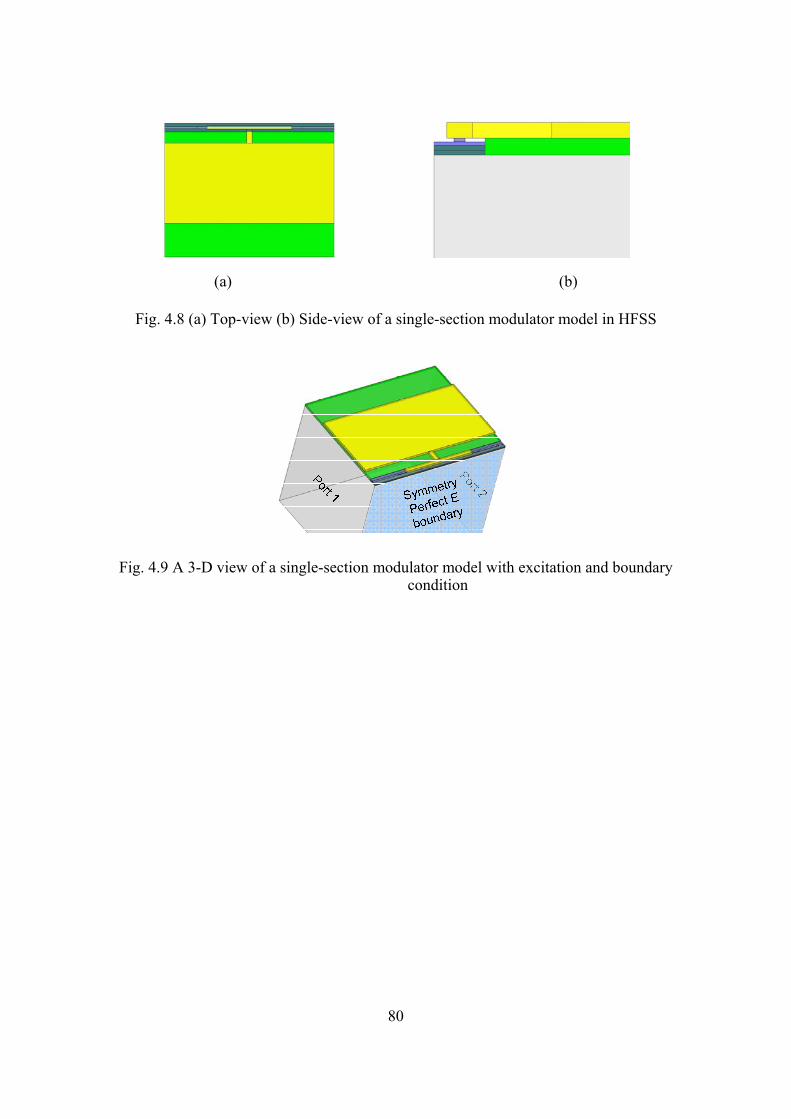
80
(a) (b)
Fig. 4.8 (a) Top-view (b) Side-view of a single-section modulator model in HFSS
Fig. 4.9 A 3-D view of a single-section modulator model with excitation and boundary condition
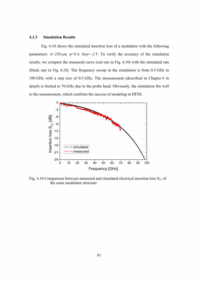
81
4.1.3 Simulation Results
Fig. 4.10 shows the simulated insertion loss of a modulator with the following
parameters: Λ=250 μm, η=0.4, bias=-2 V. To verify the accuracy of the simulation
results, we compare the measured curve (red one in Fig. 4.10) with the simulated one
(black one in Fig. 4.10). The frequency sweep in the simulation is from 0.5 GHz to
100 GHz with a step size of 0.5 GHz. The measurement (described in Chapter 6 in
detail) is limited to 70 GHz due to the probe head. Obviously, the simulation fits well
to the measurement, which confirms the success of modeling in HFSS.
0 10 20 30 40 50 60 70 80 90 100-24
-21
-18
-15
-12
-9
-6
-3
0
Inse
rtion
loss
S21
[dB
]
Frequency [GHz]
simulated measured
Fig. 4.10 Comparison between measured and simulated electrical insertion loss S21 of the same modulator structure
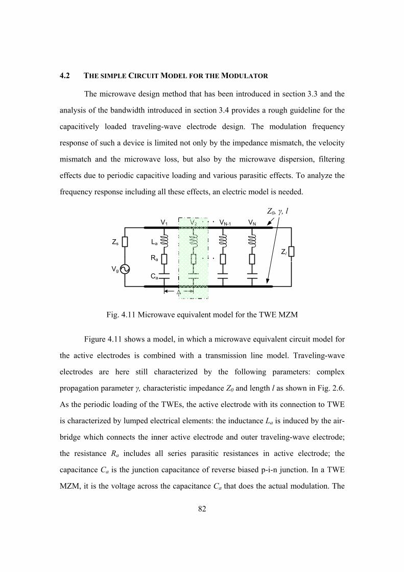
82
4.2 THE SIMPLE CIRCUIT MODEL FOR THE MODULATOR
The microwave design method that has been introduced in section 3.3 and the
analysis of the bandwidth introduced in section 3.4 provides a rough guideline for the
capacitively loaded traveling-wave electrode design. The modulation frequency
response of such a device is limited not only by the impedance mismatch, the velocity
mismatch and the microwave loss, but also by the microwave dispersion, filtering
effects due to periodic capacitive loading and various parasitic effects. To analyze the
frequency response including all these effects, an electric model is needed.
La
Vg
Zs
Zl
Λ
. . .
V1 V2 VNVN-1. . .
Ra
Ca
Z0, γ, l
Fig. 4.11 Microwave equivalent model for the TWE MZM
Figure 4.11 shows a model, in which a microwave equivalent circuit model for
the active electrodes is combined with a transmission line model. Traveling-wave
electrodes are here still characterized by the following parameters: complex
propagation parameter γ, characteristic impedance Z0 and length l as shown in Fig. 2.6.
As the periodic loading of the TWEs, the active electrode with its connection to TWE
is characterized by lumped electrical elements: the inductance La is induced by the air-
bridge which connects the inner active electrode and outer traveling-wave electrode;
the resistance Ra includes all series parasitic resistances in active electrode; the
capacitance Ca is the junction capacitance of reverse biased p-i-n junction. In a TWE
MZM, it is the voltage across the capacitance Ca that does the actual modulation. The
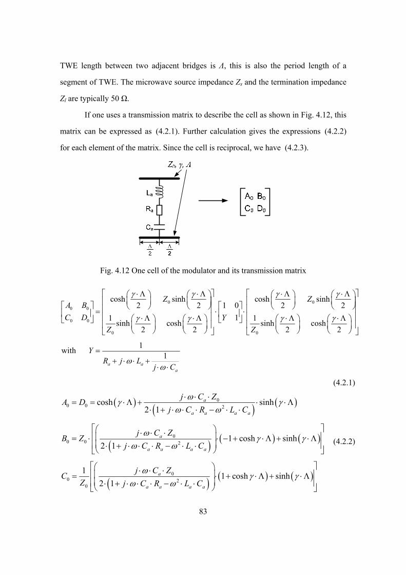
83
TWE length between two adjacent bridges is Λ, this is also the period length of a
segment of TWE. The microwave source impedance Zs and the termination impedance
Zl are typically 50 Ω.
If one uses a transmission matrix to describe the cell as shown in Fig. 4.12, this
matrix can be expressed as (4.2.1). Further calculation gives the expressions (4.2.2)
for each element of the matrix. Since the cell is reciprocal, we have (4.2.3).
Fig. 4.12 One cell of the modulator and its transmission matrix
0 00 0
0 0
0 0
cosh sinh cosh sinh1 02 2 2 2
11 1sinh cosh sinh cosh2 2 2 2
1with 1a a
Z ZA BC D Y
Z Z
YR j L
j
γ γ γ γ
γ γ γ γ
ωω
⎡ ⎤ ⎡ ⎤⋅Λ ⋅Λ ⋅Λ ⋅Λ⎛ ⎞ ⎛ ⎞ ⎛ ⎞ ⎛ ⎞⎜ ⎟ ⎜ ⎟ ⎜ ⎟ ⎜ ⎟⎢ ⎥ ⎢ ⎥⎡ ⎤ ⎡ ⎤⎝ ⎠ ⎝ ⎠ ⎝ ⎠ ⎝ ⎠⎢ ⎥ ⎢ ⎥= ⋅ ⋅⎢ ⎥ ⎢ ⎥⎢ ⎥ ⎢ ⎥⋅Λ ⋅Λ ⋅Λ ⋅Λ⎛ ⎞ ⎛ ⎞ ⎛ ⎞ ⎛ ⎞⎣ ⎦⎣ ⎦
⎢ ⎥ ⎢ ⎥⎜ ⎟ ⎜ ⎟ ⎜ ⎟ ⎜ ⎟⎝ ⎠ ⎝ ⎠ ⎝ ⎠ ⎝ ⎠⎣ ⎦ ⎣ ⎦
=+ ⋅ ⋅ +
⋅ aC⋅
(4.2.1)
( ) ( ) ( )
( ) ( ) ( )
( ) ( ) ( )
00 0 2
00 0 2
00 2
0
cosh sinh2 1
1 cosh sinh2 1
1 1 cosh sinh2 1
a
a a a a
a
a a a a
a
a a a a
j C ZA Dj C R L C
j C ZB Zj C R L C
j C ZCZ j C R L C
ωγ γω ω
ω γ γω ω
ω γ γω ω
⋅ ⋅ ⋅= = ⋅Λ + ⋅ ⋅ Λ
⋅ + ⋅ ⋅ ⋅ − ⋅ ⋅
⎡ ⎤⎛ ⎞⋅ ⋅ ⋅⎢ ⎥⎜ ⎟= ⋅ ⋅ − + ⋅ Λ + ⋅Λ⎜ ⎟⎢ ⎥⋅ + ⋅ ⋅ ⋅ − ⋅ ⋅⎝ ⎠⎣ ⎦
⎡ ⎤⎛ ⎞⋅ ⋅ ⋅⎢ ⎥⎜ ⎟= ⋅ + ⋅ Λ + ⋅ Λ⎜ ⎟⎢ ⎥⋅ + ⋅ ⋅ ⋅ − ⋅ ⋅⎝ ⎠⎣ ⎦
(4.2.2)
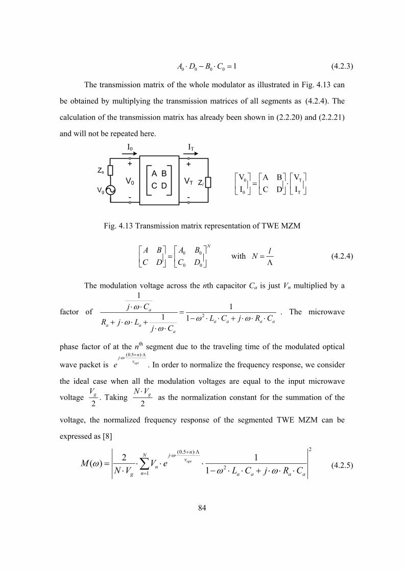
84
0 0 0 0 1A D B C⋅ − ⋅ = (4.2.3)
The transmission matrix of the whole modulator as illustrated in Fig. 4.13 can
be obtained by multiplying the transmission matrices of all segments as (4.2.4). The
calculation of the transmission matrix has already been shown in (2.2.20) and (2.2.21)
and will not be repeated here.
Vg
Zs
Zl
A BC D
+ +
--
V0 VT
I0 IT
0 T
0 T
V VA BI IC D
⎡ ⎤ ⎡ ⎤⎡ ⎤= ⋅⎢ ⎥ ⎢ ⎥⎢ ⎥
⎣ ⎦ ⎣ ⎦⎣ ⎦
Fig. 4.13 Transmission matrix representation of TWE MZM
0 0
0 0
with NA BA B lN
C DC D⎡ ⎤⎡ ⎤
= =⎢ ⎥⎢ ⎥ Λ⎣ ⎦ ⎣ ⎦ (4.2.4)
The modulation voltage across the nth capacitor Ca is just Vn multiplied by a
factor of 2
11
1 1a
a a a aa a
a
j CL C j R CR j L
j C
ωω ωω
ω
⋅ ⋅=
− ⋅ ⋅ + ⋅ ⋅ ⋅+ ⋅ ⋅ +⋅ ⋅
. The microwave
phase factor of at the nth segment due to the traveling time of the modulated optical
wave packet is (0.5 )
opt
njve
ω + ⋅Λ⋅ ⋅
. In order to normalize the frequency response, we consider
the ideal case when all the modulation voltages are equal to the input microwave
voltage 2gV
. Taking 2
gN V⋅ as the normalization constant for the summation of the
voltage, the normalized frequency response of the segmented TWE MZM can be
expressed as [8] 2(0.5 )
21
2 1( )1
opt
nN jv
nng a a a a
M V eN V L C j R C
ω
ωω ω
+ ⋅Λ⋅ ⋅
=
= ⋅ ⋅ ⋅⋅ − ⋅ ⋅ + ⋅ ⋅ ⋅∑ (4.2.5)
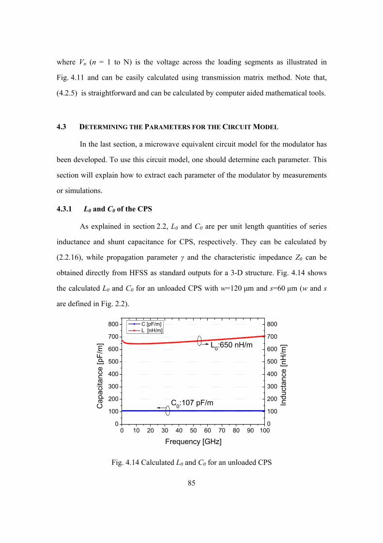
85
where Vn (n = 1 to N) is the voltage across the loading segments as illustrated in
Fig. 4.11 and can be easily calculated using transmission matrix method. Note that,
(4.2.5) is straightforward and can be calculated by computer aided mathematical tools.
4.3 DETERMINING THE PARAMETERS FOR THE CIRCUIT MODEL
In the last section, a microwave equivalent circuit model for the modulator has
been developed. To use this circuit model, one should determine each parameter. This
section will explain how to extract each parameter of the modulator by measurements
or simulations.
4.3.1 L0 and C0 of the CPS
As explained in section 2.2, L0 and C0 are per unit length quantities of series
inductance and shunt capacitance for CPS, respectively. They can be calculated by
(2.2.16), while propagation parameter γ and the characteristic impedance Z0 can be
obtained directly from HFSS as standard outputs for a 3-D structure. Fig. 4.14 shows
the calculated L0 and C0 for an unloaded CPS with w=120 μm and s=60 μm (w and s
are defined in Fig. 2.2).
0 10 20 30 40 50 60 70 80 90 1000
100
200
300
400
500
600
700
800
0
100
200
300
400
500
600
700
800
C0:107 pF/m Indu
ctan
ce [n
H/m
]
Cap
acita
nce
[pF/
m]
Frequency [GHz]
C [pF/m] L [nH/m]
L0:650 nH/m
Fig. 4.14 Calculated L0 and C0 for an unloaded CPS
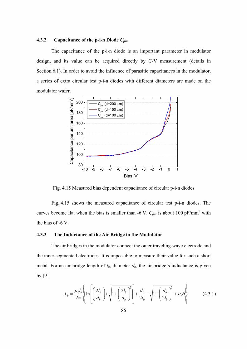
86
4.3.2 Capacitance of the p-i-n Diode Cpin
The capacitance of the p-i-n diode is an important parameter in modulator
design, and its value can be acquired directly by C-V measurement (details in
Section 6.1). In order to avoid the influence of parasitic capacitances in the modulator,
a series of extra circular test p-i-n diodes with different diameters are made on the
modulator wafer.
-10 -9 -8 -7 -6 -5 -4 -3 -2 -1 0 180
100
120
140
160
180
200
Cap
acita
nce
per u
nit a
rea
[pF/
mm
2 ]
Bias [V]
Cpin (d=200 μm) Cpin (d=150 μm) Cpin (d=100 μm)
Fig. 4.15 Measured bias dependent capacitance of circular p-i-n diodes
Fig. 4.15 shows the measured capacitance of circular test p-i-n diodes. The
curves become flat when the bias is smaller than -6 V. Cpin is about 100 pF/mm2 with
the bias of -6 V.
4.3.3 The Inductance of the Air Bridge in the Modulator
The air bridges in the modulator connect the outer traveling-wave electrode and
the inner segmented electrodes. It is impossible to measure their value for such a short
metal. For an air-bridge length of lb, diameter db, the air-bridge’s inductance is given
by [9]
2 2
0 2 2ln 1 12 2 2
b b b b bb r
b b b b
l l l d dLd d l l
μ μ δπ
⎧ ⎫⎡ ⎤⎛ ⎞ ⎛ ⎞ ⎛ ⎞⎪ ⎪⎢ ⎥= + + + − + +⎨ ⎬⎜ ⎟ ⎜ ⎟ ⎜ ⎟⎢ ⎥⎝ ⎠ ⎝ ⎠ ⎝ ⎠⎪ ⎪⎣ ⎦⎩ ⎭
(4.3.1)
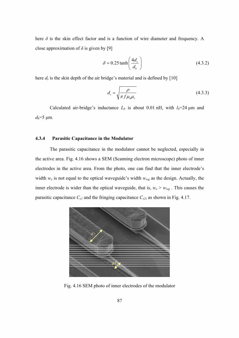
87
here δ is the skin effect factor and is a function of wire diameter and frequency. A
close approximation of δ is given by [9]
40.25 tanh s
b
dd
δ⎛ ⎞
= ⎜ ⎟⎝ ⎠
(4.3.2)
here ds is the skin depth of the air bridge’s material and is defined by [10]
0
sr
df
ρπ μ μ
= (4.3.3)
Calculated air-bridge’s inductance Lb is about 0.01 nH, with lb=24 μm and
db=5 μm.
4.3.4 Parasitic Capacitance in the Modulator
The parasitic capacitance in the modulator cannot be neglected, especially in
the active area. Fig. 4.16 shows a SEM (Scanning electron microscope) photo of inner
electrodes in the active area. From the photo, one can find that the inner electrode’s
width we is not equal to the optical waveguide’s width wwg as the design. Actually, the
inner electrode is wider than the optical waveguide, that is, we > wwg . This causes the
parasitic capacitance Cs1 and the fringing capacitance Cs2, as shown in Fig. 4.17.
Fig. 4.16 SEM photo of inner electrodes of the modulator
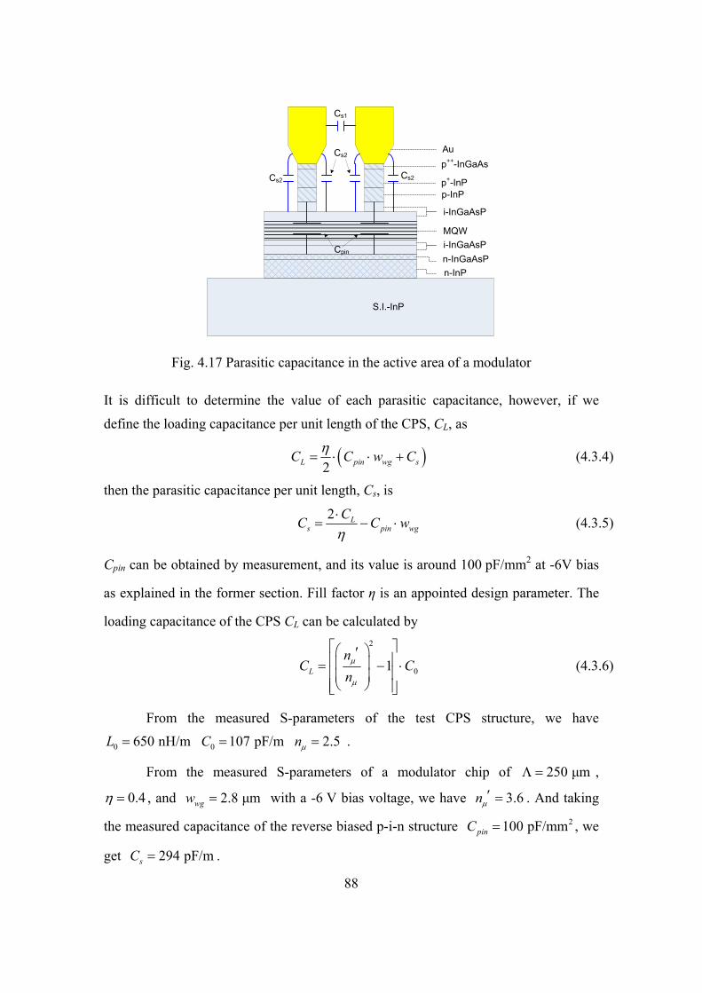
88
n-InPn-InGaAsP
p+-InP
p++-InGaAs
MQW
p-InP
i-InGaAsP
i-InGaAsP
Au
S.I.-InP
Cs2
Cs1
Cs2
Cpin
Cs2
Fig. 4.17 Parasitic capacitance in the active area of a modulator
It is difficult to determine the value of each parasitic capacitance, however, if we
define the loading capacitance per unit length of the CPS, CL, as
( )2L pin wg sC C w Cη= ⋅ ⋅ + (4.3.4)
then the parasitic capacitance per unit length, Cs, is
2 Ls pin wg
CC C wη⋅
= − ⋅ (4.3.5)
Cpin can be obtained by measurement, and its value is around 100 pF/mm2 at -6V bias
as explained in the former section. Fill factor η is an appointed design parameter. The
loading capacitance of the CPS CL can be calculated by
2
01L
nC C
nμ
μ
⎡ ⎤⎛ ⎞′⎢ ⎥⎜ ⎟= − ⋅⎢ ⎥⎜ ⎟⎝ ⎠⎢ ⎥⎣ ⎦
(4.3.6)
From the measured S-parameters of the test CPS structure, we have
0 0650 nH/m 107 pF/m 2.5 L C nμ= = = .
From the measured S-parameters of a modulator chip of 250 μmΛ = ,
0.4η = , and 2.8 μmwgw = with a -6 V bias voltage, we have 3.6nμ′ = . And taking
the measured capacitance of the reverse biased p-i-n structure 2100 pF/mmpinC = , we
get 294 pF/msC = .
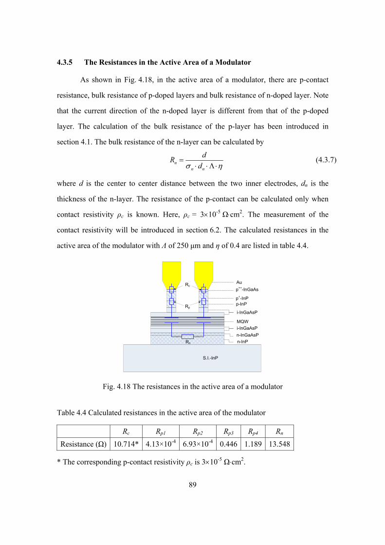
89
4.3.5 The Resistances in the Active Area of a Modulator
As shown in Fig. 4.18, in the active area of a modulator, there are p-contact
resistance, bulk resistance of p-doped layers and bulk resistance of n-doped layer. Note
that the current direction of the n-doped layer is different from that of the p-doped
layer. The calculation of the bulk resistance of the p-layer has been introduced in
section 4.1. The bulk resistance of the n-layer can be calculated by
nn n
dRdσ η
=⋅ ⋅Λ ⋅
(4.3.7)
where d is the center to center distance between the two inner electrodes, dn is the
thickness of the n-layer. The resistance of the p-contact can be calculated only when
contact resistivity ρc is known. Here, ρc = 3×10⁻⁵ Ω⋅cm2. The measurement of the
contact resistivity will be introduced in section 6.2. The calculated resistances in the
active area of the modulator with Λ of 250 μm and η of 0.4 are listed in table 4.4.
n-InPn-InGaAsP
p+-InP
p++-InGaAs
MQW
p-InP
i-InGaAsP
i-InGaAsP
Au
S.I.-InP
Rc
Rp
Rn
Fig. 4.18 The resistances in the active area of a modulator
Table 4.4 Calculated resistances in the active area of the modulator
Rc Rp1 Rp2 Rp3 Rp4 Rn
Resistance (Ω) 10.714* 4.13×10-4 6.93×10⁻⁴ 0.446 1.189 13.548
* The corresponding p-contact resistivity ρc is 3×10⁻⁵ Ω⋅cm2.
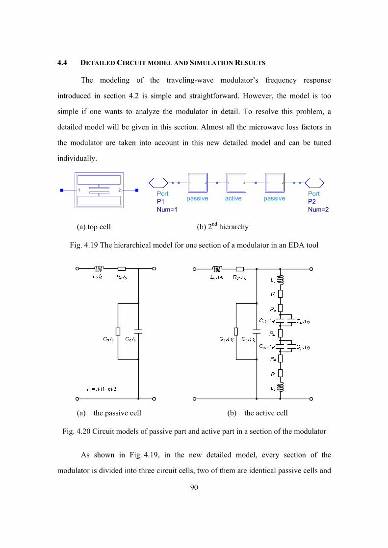
90
4.4 DETAILED CIRCUIT MODEL AND SIMULATION RESULTS
The modeling of the traveling-wave modulator’s frequency response
introduced in section 4.2 is simple and straightforward. However, the model is too
simple if one wants to analyze the modulator in detail. To resolve this problem, a
detailed model will be given in this section. Almost all the microwave loss factors in
the modulator are taken into account in this new detailed model and can be tuned
individually.
21
PortP2Num=2
passiveX2
21
activeX3
21
PortP1Num=1
passiveX1
21
(a) top cell (b) 2nd hierarchy
Fig. 4.19 The hierarchical model for one section of a modulator in an EDA tool
(a) the passive cell (b) the active cell
Fig. 4.20 Circuit models of passive part and active part in a section of the modulator
As shown in Fig. 4.19, in the new detailed model, every section of the
modulator is divided into three circuit cells, two of them are identical passive cells and
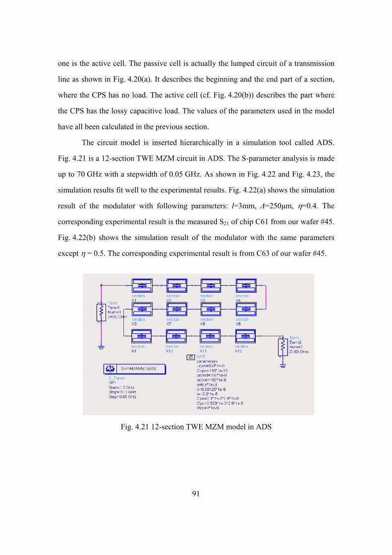
91
one is the active cell. The passive cell is actually the lumped circuit of a transmission
line as shown in Fig. 4.20(a). It describes the beginning and the end part of a section,
where the CPS has no load. The active cell (cf. Fig. 4.20(b)) describes the part where
the CPS has the lossy capacitive load. The values of the parameters used in the model
have all been calculated in the previous section.
The circuit model is inserted hierarchically in a simulation tool called ADS.
Fig. 4.21 is a 12-section TWE MZM circuit in ADS. The S-parameter analysis is made
up to 70 GHz with a stepwidth of 0.05 GHz. As shown in Fig. 4.22 and Fig. 4.23, the
simulation results fit well to the experimental results. Fig. 4.22(a) shows the simulation
result of the modulator with following parameters: l=3mm, Λ=250μm, η=0.4. The
corresponding experimental result is the measured S21 of chip C61 from our wafer #45.
Fig. 4.22(b) shows the simulation result of the modulator with the same parameters
except η = 0.5. The corresponding experimental result is from C63 of our wafer #45.
Fig. 4.21 12-section TWE MZM model in ADS
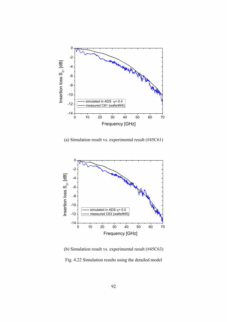
92
0 10 20 30 40 50 60 70-14
-12
-10
-8
-6
-4
-2
0
Inse
rtion
loss
S21
[dB
]
Frequency [GHz]
simulated in ADS η= 0.4 measured C61 (wafer#45)
(a) Simulation result vs. experimental result (#45C61)
0 10 20 30 40 50 60 70-14
-12
-10
-8
-6
-4
-2
0
Inse
rtion
loss
S21
[dB
]
Frequency [GHz]
simulated in ADS η= 0.5 measured C63 (wafer#45)
(b) Simulation result vs. experimental result (#45C63)
Fig. 4.22 Simulation results using the detailed model
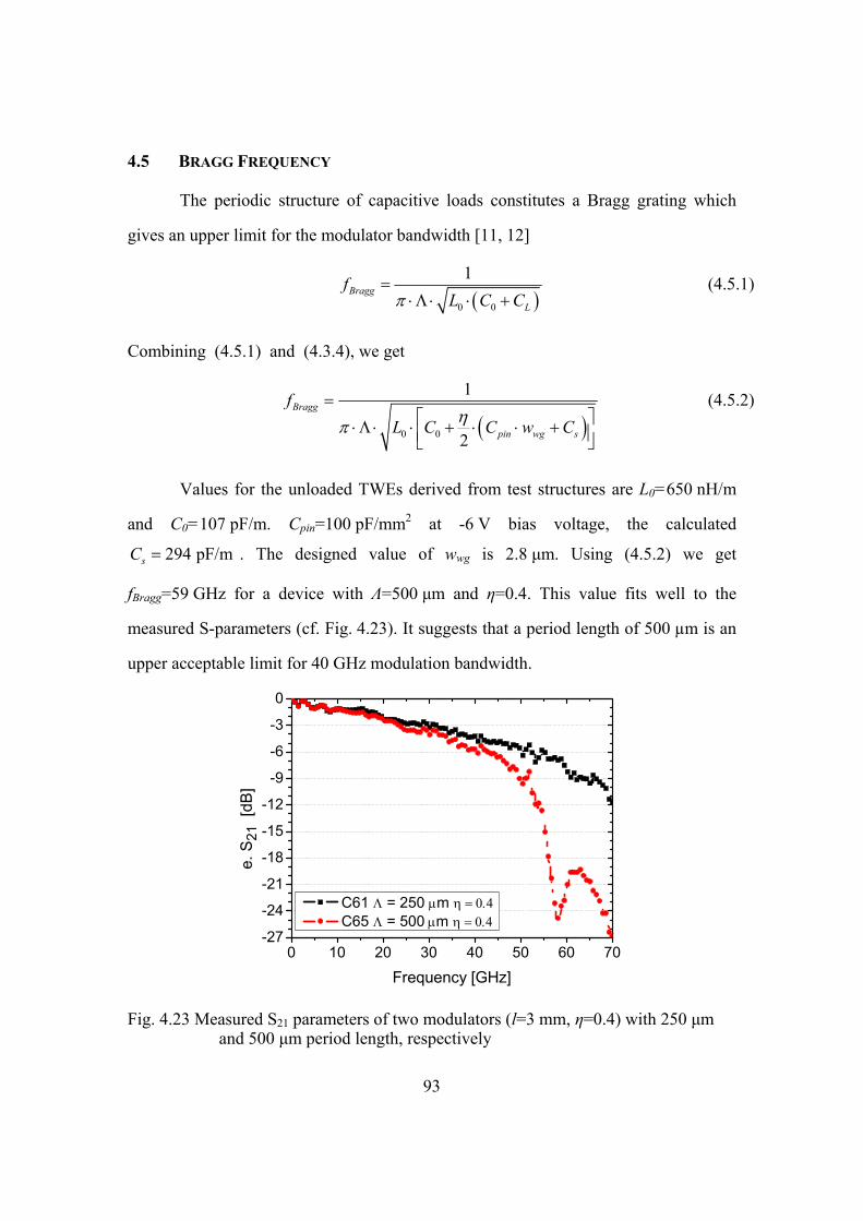
93
4.5 BRAGG FREQUENCY
The periodic structure of capacitive loads constitutes a Bragg grating which
gives an upper limit for the modulator bandwidth [11, 12]
( )0 0
1Bragg
L
fL C Cπ
=⋅ Λ ⋅ ⋅ +
(4.5.1)
Combining (4.5.1) and (4.3.4), we get
( )0 0
1
2
Bragg
pin wg s
fL C C w Cηπ
=⎡ ⎤⋅ Λ ⋅ ⋅ + ⋅ ⋅ +⎢ ⎥⎣ ⎦
(4.5.2)
Values for the unloaded TWEs derived from test structures are L0=650 nH/m
and C0=107 pF/m. Cpin=100 pF/mm2 at -6 V bias voltage, the calculated
294 pF/msC = . The designed value of wwg is 2.8 μm. Using (4.5.2) we get
fBragg=59 GHz for a device with Λ=500 μm and η=0.4. This value fits well to the
measured S-parameters (cf. Fig. 4.23). It suggests that a period length of 500 µm is an
upper acceptable limit for 40 GHz modulation bandwidth.
0 10 20 30 40 50 60 70-27
-24
-21
-18
-15
-12
-9
-6
-3
0
e. S
21 [
dB]
Frequency [GHz]
C61 Λ = 250 μm η = 0.4 C65 Λ = 500 μm η = 0.4
Fig. 4.23 Measured S21 parameters of two modulators (l=3 mm, η=0.4) with 250 μm and 500 μm period length, respectively
94
Taking (3.3.4) into (4.5.1), we get
'Bragg
cfnμπ
=⋅ Λ ⋅
(4.5.3)
This means the Bragg frequency can be calculated with the following parameters: the
period length and the microwave index of the modulator. As the design target, the
microwave index should equal the optical index in a modulator. So, we can calculate
the maximum period length using (4.5.4) under the condition that the Bragg
frequency should be kept far away from the modulation frequency range, or in other
words, the operation speed of the modulator should not be limited by the Bragg
frequency in the frequency range of interest.
opt
cf nπ
Λ ≤⋅ ⋅
(4.5.4)
Taking nopt = 3.7, we get Λ ≤ 323 μm and Λ ≤ 252 μm for f = 80 GHz and f =
100 GHz, respectively. Hence, we choose 250 µm as well as 125 µm as period length
for the modulators which are designed to work up to 80 Gbit/s or a higher speed.
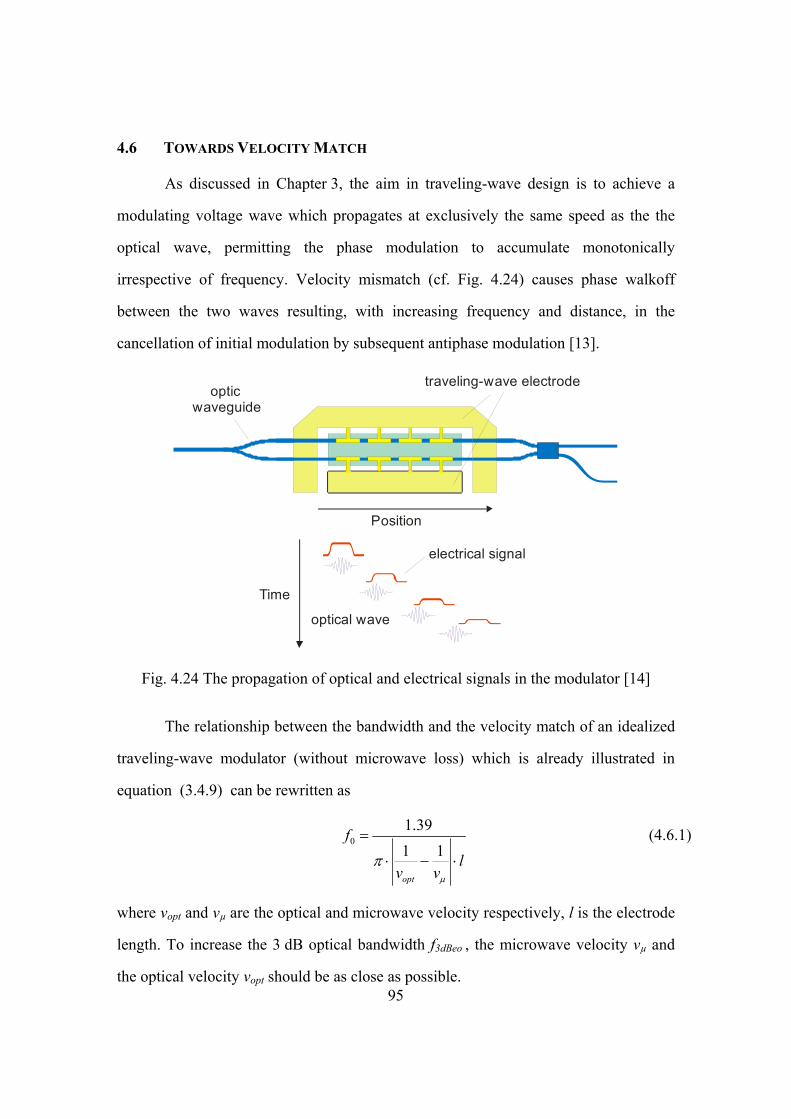
95
4.6 TOWARDS VELOCITY MATCH
As discussed in Chapter 3, the aim in traveling-wave design is to achieve a
modulating voltage wave which propagates at exclusively the same speed as the the
optical wave, permitting the phase modulation to accumulate monotonically
irrespective of frequency. Velocity mismatch (cf. Fig. 4.24) causes phase walkoff
between the two waves resulting, with increasing frequency and distance, in the
cancellation of initial modulation by subsequent antiphase modulation [13].
optical wave
Time
Position
optic waveguide
traveling-wave electrode
electrical signal
Fig. 4.24 The propagation of optical and electrical signals in the modulator [14]
The relationship between the bandwidth and the velocity match of an idealized
traveling-wave modulator (without microwave loss) which is already illustrated in
equation (3.4.9) can be rewritten as
01.391 1
opt
fl
v vμ
π=
⋅ − ⋅
(4.6.1)
where vopt and vµ are the optical and microwave velocity respectively, l is the electrode
length. To increase the 3 dB optical bandwidth f3dBeo , the microwave velocity vµ and
the optical velocity vopt should be as close as possible.
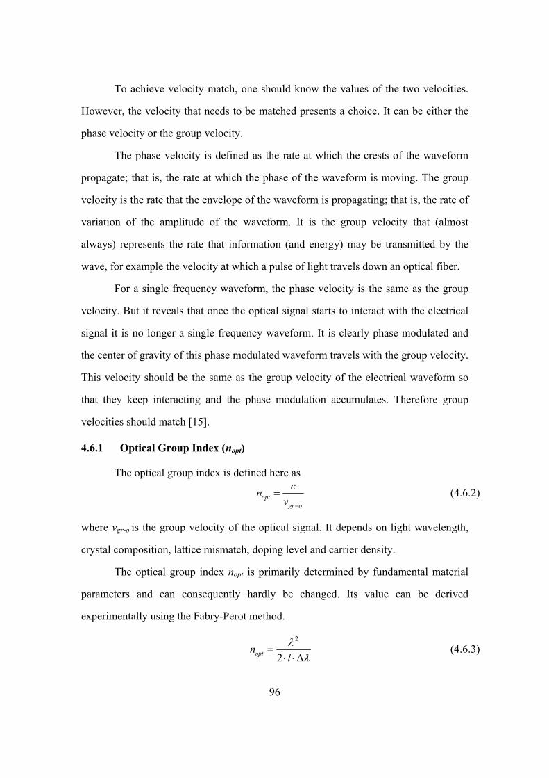
96
To achieve velocity match, one should know the values of the two velocities.
However, the velocity that needs to be matched presents a choice. It can be either the
phase velocity or the group velocity.
The phase velocity is defined as the rate at which the crests of the waveform
propagate; that is, the rate at which the phase of the waveform is moving. The group
velocity is the rate that the envelope of the waveform is propagating; that is, the rate of
variation of the amplitude of the waveform. It is the group velocity that (almost
always) represents the rate that information (and energy) may be transmitted by the
wave, for example the velocity at which a pulse of light travels down an optical fiber.
For a single frequency waveform, the phase velocity is the same as the group
velocity. But it reveals that once the optical signal starts to interact with the electrical
signal it is no longer a single frequency waveform. It is clearly phase modulated and
the center of gravity of this phase modulated waveform travels with the group velocity.
This velocity should be the same as the group velocity of the electrical waveform so
that they keep interacting and the phase modulation accumulates. Therefore group
velocities should match [15].
4.6.1 Optical Group Index (nopt)
The optical group index is defined here as
optgr o
cnv −
= (4.6.2)
where vgr-o is the group velocity of the optical signal. It depends on light wavelength,
crystal composition, lattice mismatch, doping level and carrier density.
The optical group index nopt is primarily determined by fundamental material
parameters and can consequently hardly be changed. Its value can be derived
experimentally using the Fabry-Perot method.
2
2optnlλ
λ=
⋅ ⋅Δ (4.6.3)
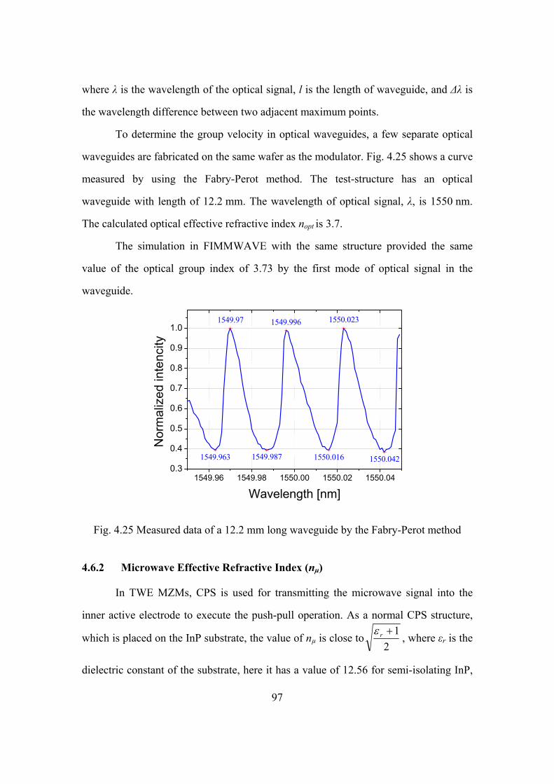
97
where λ is the wavelength of the optical signal, l is the length of waveguide, and Δλ is
the wavelength difference between two adjacent maximum points.
To determine the group velocity in optical waveguides, a few separate optical
waveguides are fabricated on the same wafer as the modulator. Fig. 4.25 shows a curve
measured by using the Fabry-Perot method. The test-structure has an optical
waveguide with length of 12.2 mm. The wavelength of optical signal, λ, is 1550 nm.
The calculated optical effective refractive index nopt is 3.7.
The simulation in FIMMWAVE with the same structure provided the same
value of the optical group index of 3.73 by the first mode of optical signal in the
waveguide.
1549.96 1549.98 1550.00 1550.02 1550.040.3
0.4
0.5
0.6
0.7
0.8
0.9
1.01549.97 1549.996 1550.023
1549.963 1549.987 1550.016 1550.042
Nor
mal
ized
inte
ncity
Wavelength [nm]
Fig. 4.25 Measured data of a 12.2 mm long waveguide by the Fabry-Perot method
4.6.2 Microwave Effective Refractive Index (nμ)
In TWE MZMs, CPS is used for transmitting the microwave signal into the
inner active electrode to execute the push-pull operation. As a normal CPS structure,
which is placed on the InP substrate, the value of nµ is close to2
1+rε , where εr is the
dielectric constant of the substrate, here it has a value of 12.56 for semi-isolating InP,
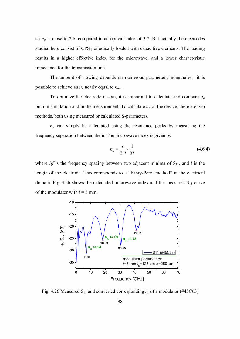
98
so nµ is close to 2.6, compared to an optical index of 3.7. But actually the electrodes
studied here consist of CPS periodically loaded with capacitive elements. The loading
results in a higher effective index for the microwave, and a lower characteristic
impedance for the transmission line.
The amount of slowing depends on numerous parameters; nonetheless, it is
possible to achieve an nµ nearly equal to nopt.
To optimize the electrode design, it is important to calculate and compare nµ
both in simulation and in the measurement. To calculate nµ of the device, there are two
methods, both using measured or calculated S-parameters.
nµ can simply be calculated using the resonance peaks by measuring the
frequency separation between them. The microwave index is given by
12cn
l fμ = ⋅⋅ Δ
(4.6.4)
where Δf is the frequency spacing between two adjacent minima of S11, and l is the
length of the electrode. This corresponds to a “Fabry-Perot method” in the electrical
domain. Fig. 4.26 shows the calculated microwave index and the measured S11 curve
of the modulator with l = 3 mm.
0 10 20 30 40 50 60 70
-35
-30
-25
-20
-15
-10
6.81
18.3330.55
41.02
modulator parameters:l=3 mm lE=125 μm Λ=250 μm
nμ3=4.78nμ2=4.09
e. S
11 [d
B]
Frequency [GHz]
S11 (#45C63)nμ1=4.34
Fig. 4.26 Measured S11 and converted corresponding nμ of a modulator (#45C63)
99
However, nµ is not a constant for the whole frequency range (cf. Fig. 4.27b).
The method introduced above cannot express the difference of nµ in different
frequency areas and the calculated nµ is also influenced strongly by Δf, which is
limited by the inaccuracy of measurement (cf. Fig. 4.26). It can be seen that the
calculated nµ in Fig. 4.26 changes between 4.09 and 4.78.
The microwave effective refractive index nμ can also be derived using the
phase part of S21 parameters according to
lf
cffn⋅⋅⋅
⋅=
πφ
μ 2)()( (4.6.5)
where φ(f) is converted accumulated phase delay of S21 in rad. Using this method one
can get a precise curve describing nµ as a function of frequency.
To compare the difference of the two methods, the same modulator’s measured
data are used for the calculation again. Fig. 4.27(a) shows the phase part of the
measured S21 of the modulator. These phases are converted into accumulated phase
delay as its zero point is set by frequency of 0. In Fig. 4.27(b) the blue curve represents
the phase delay in unit of radian, the black one is the corresponding curve of the
calculated microwave index using (4.6.5). The calculated microwave index is
ascending as the frequency increases, because the parasitic capacitance in the active
area of a modulator is increasing as the working frequency ascends.
0 10 20 30 40 50 60 70
-180
-120
-60
0
60
120
180
θ 21
Frequency [GHz] 0 10 20 30 40 50 60 70
3.0
3.3
3.6
3.9
4.2
4.5
4.8
microwave effective refractive index accumulated phase delay of S21
Frequency [GHz]
n μ (f)
-21
-18
-15
-12
-9
-6
-3
0
φ(f) [rad]
(a) Measured phase of S21 (b) Converted accumulated phase delay of S21 and nμ
Fig. 4.27 Measured phase and converted corresponding nμ of a modulator (#45C63)
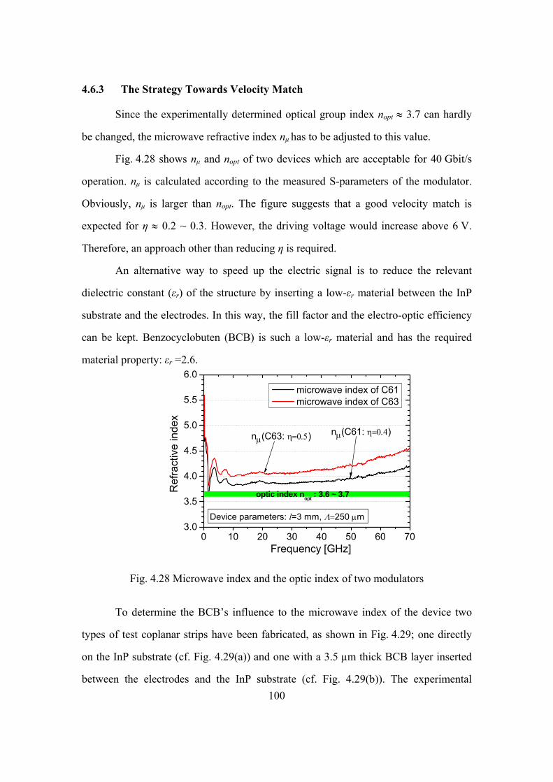
100
4.6.3 The Strategy Towards Velocity Match
Since the experimentally determined optical group index nopt ≈ 3.7 can hardly
be changed, the microwave refractive index nμ has to be adjusted to this value.
Fig. 4.28 shows nμ and nopt of two devices which are acceptable for 40 Gbit/s
operation. nμ is calculated according to the measured S-parameters of the modulator.
Obviously, nμ is larger than nopt. The figure suggests that a good velocity match is
expected for η ≈ 0.2 ~ 0.3. However, the driving voltage would increase above 6 V.
Therefore, an approach other than reducing η is required.
An alternative way to speed up the electric signal is to reduce the relevant
dielectric constant (εr) of the structure by inserting a low-εr material between the InP
substrate and the electrodes. In this way, the fill factor and the electro-optic efficiency
can be kept. Benzocyclobuten (BCB) is such a low-εr material and has the required
material property: εr =2.6.
0 10 20 30 40 50 60 703.0
3.5
4.0
4.5
5.0
5.5
6.0
nμ(C61: η=0.4)
Ref
ract
ive
inde
x
Frequency [GHz]
microwave index of C61 microwave index of C63
optic index nopt : 3.6 ~ 3.7
Device parameters: l=3 mm, Λ=250 μm
nμ(C63: η=0.5)
Fig. 4.28 Microwave index and the optic index of two modulators
To determine the BCB’s influence to the microwave index of the device two
types of test coplanar strips have been fabricated, as shown in Fig. 4.29; one directly
on the InP substrate (cf. Fig. 4.29(a)) and one with a 3.5 µm thick BCB layer inserted
between the electrodes and the InP substrate (cf. Fig. 4.29(b)). The experimental
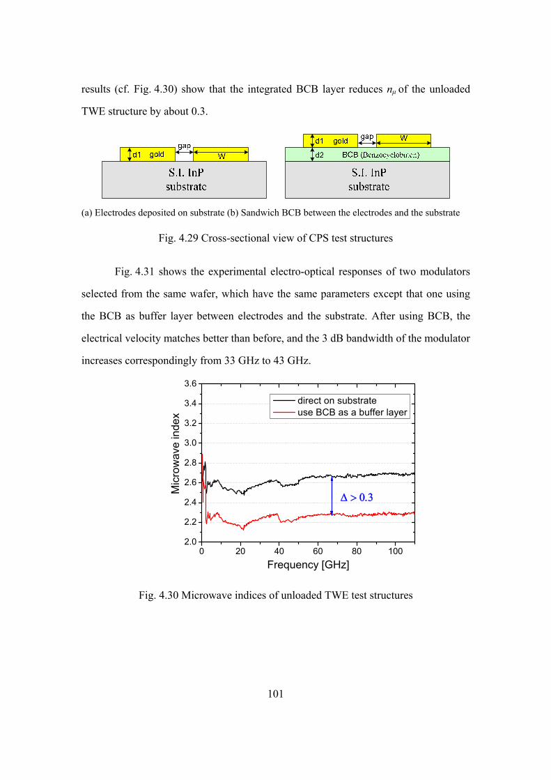
101
results (cf. Fig. 4.30) show that the integrated BCB layer reduces nμ of the unloaded
TWE structure by about 0.3.
(a) Electrodes deposited on substrate (b) Sandwich BCB between the electrodes and the substrate
Fig. 4.29 Cross-sectional view of CPS test structures
Fig. 4.31 shows the experimental electro-optical responses of two modulators
selected from the same wafer, which have the same parameters except that one using
the BCB as buffer layer between electrodes and the substrate. After using BCB, the
electrical velocity matches better than before, and the 3 dB bandwidth of the modulator
increases correspondingly from 33 GHz to 43 GHz.
0 20 40 60 80 1002.0
2.2
2.4
2.6
2.8
3.0
3.2
3.4
3.6
Mic
row
ave
inde
x
Frequency [GHz]
direct on substrate use BCB as a buffer layer
Δ > 0.3
Fig. 4.30 Microwave indices of unloaded TWE test structures
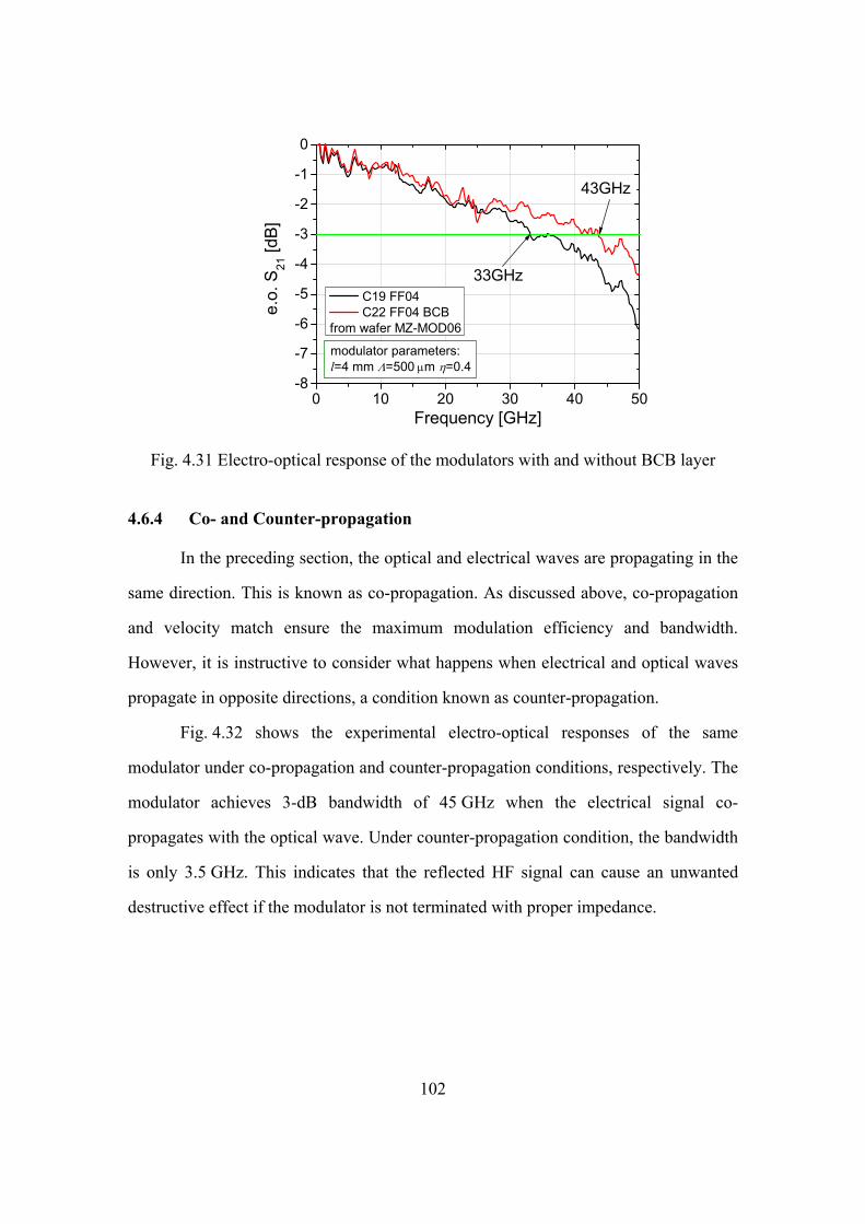
102
0 10 20 30 40 50-8
-7
-6
-5
-4
-3
-2
-1
0
e.o.
S21
[dB]
Frequency [GHz]
C19 FF04 C22 FF04 BCB
from wafer MZ-MOD06
33GHz
43GHz
modulator parameters:l=4 mm Λ=500 μm η=0.4
Fig. 4.31 Electro-optical response of the modulators with and without BCB layer
4.6.4 Co- and Counter-propagation
In the preceding section, the optical and electrical waves are propagating in the
same direction. This is known as co-propagation. As discussed above, co-propagation
and velocity match ensure the maximum modulation efficiency and bandwidth.
However, it is instructive to consider what happens when electrical and optical waves
propagate in opposite directions, a condition known as counter-propagation.
Fig. 4.32 shows the experimental electro-optical responses of the same
modulator under co-propagation and counter-propagation conditions, respectively. The
modulator achieves 3-dB bandwidth of 45 GHz when the electrical signal co-
propagates with the optical wave. Under counter-propagation condition, the bandwidth
is only 3.5 GHz. This indicates that the reflected HF signal can cause an unwanted
destructive effect if the modulator is not terminated with proper impedance.
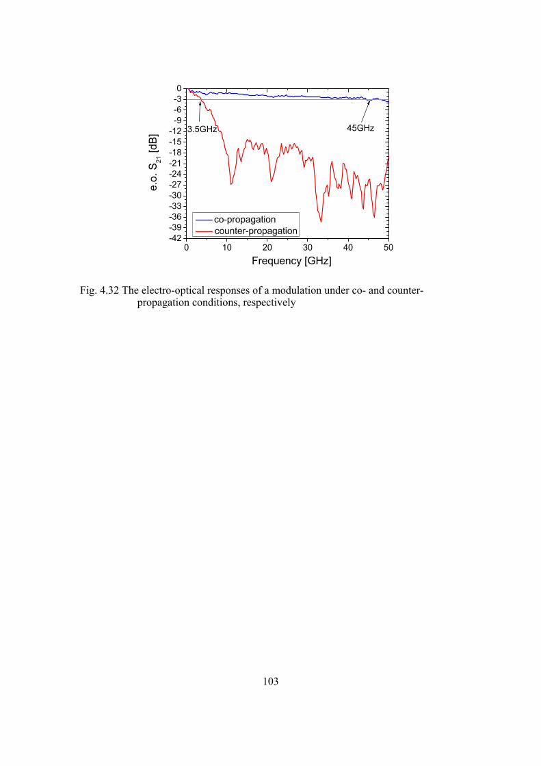
103
0 10 20 30 40 50-42-39-36-33-30-27-24-21-18-15-12-9-6-30
e.o.
S21
[dB
]
Frequency [GHz]
co-propagation counter-propagation
3.5GHz 45GHz
Fig. 4.32 The electro-optical responses of a modulation under co- and counter- propagation conditions, respectively
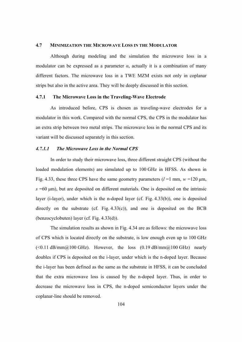
104
4.7 MINIMIZATION THE MICROWAVE LOSS IN THE MODULATOR
Although during modeling and the simulation the microwave loss in a
modulator can be expressed as a parameter α, actually it is a combination of many
different factors. The microwave loss in a TWE MZM exists not only in coplanar
strips but also in the active area. They will be deeply discussed in this section.
4.7.1 The Microwave Loss in the Traveling-Wave Electrode
As introduced before, CPS is chosen as traveling-wave electrodes for a
modulator in this work. Compared with the normal CPS, the CPS in the modulator has
an extra strip between two metal strips. The microwave loss in the normal CPS and its
variant will be discussed separately in this section.
4.7.1.1 The Microwave Loss in the Normal CPS
In order to study their microwave loss, three different straight CPS (without the
loaded modulation elements) are simulated up to 100 GHz in HFSS. As shown in
Fig. 4.33, these three CPS have the same geometry parameters (l =1 mm, w =120 μm,
s =60 μm), but are deposited on different materials. One is deposited on the intrinsic
layer (i-layer), under which is the n-doped layer (cf. Fig. 4.33(b)), one is deposited
directly on the substrate (cf. Fig. 4.33(c)), and one is deposited on the BCB
(benzocyclobuten) layer (cf. Fig. 4.33(d)).
The simulation results as shown in Fig. 4.34 are as follows: the microwave loss
of CPS which is located directly on the substrate, is low enough even up to 100 GHz
(<0.11 dB/mm@100 GHz). However, the loss (0.19 dB/mm@100 GHz) nearly
doubles if CPS is deposited on the i-layer, under which is the n-doped layer. Because
the i-layer has been defined as the same as the substrate in HFSS, it can be concluded
that the extra microwave loss is caused by the n-doped layer. Thus, in order to
decrease the microwave loss in CPS, the n-doped semiconductor layers under the
coplanar-line should be removed.
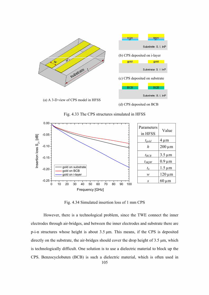
105
(b) CPS deposited on i-layer
(c) CPS deposited on substrate
(a) A 3-D view of CPS model in HFSS (d) CPS deposited on BCB
Fig. 4.33 The CPS structures simulated in HFSS
0 10 20 30 40 50 60 70 80 90 100-0.25
-0.20
-0.15
-0.10
-0.05
0.00
Inse
rtion
loss
S21
[dB
]
Frequency [GHz]
gold on substrate gold on BCB gold on i-layer
Parameters in HFSS
Value
tgold 4 μm h 200 μm
tBCB 3.5 μm tMQW 0.9 μm
tn 1.5 μm w 120 μms 60 μm
Fig. 4.34 Simulated insertion loss of 1 mm CPS
However, there is a technological problem, since the TWE connect the inner
electrodes through air-bridges, and between the inner electrodes and substrate there are
p-i-n structures whose height is about 3.5 μm. This means, if the CPS is deposited
directly on the substrate, the air-bridges should cover the drop height of 3.5 μm, which
is technologically difficult. One solution is to use a dielectric material to block up the
CPS. Benzocyclobuten (BCB) is such a dielectric material, which is often used in
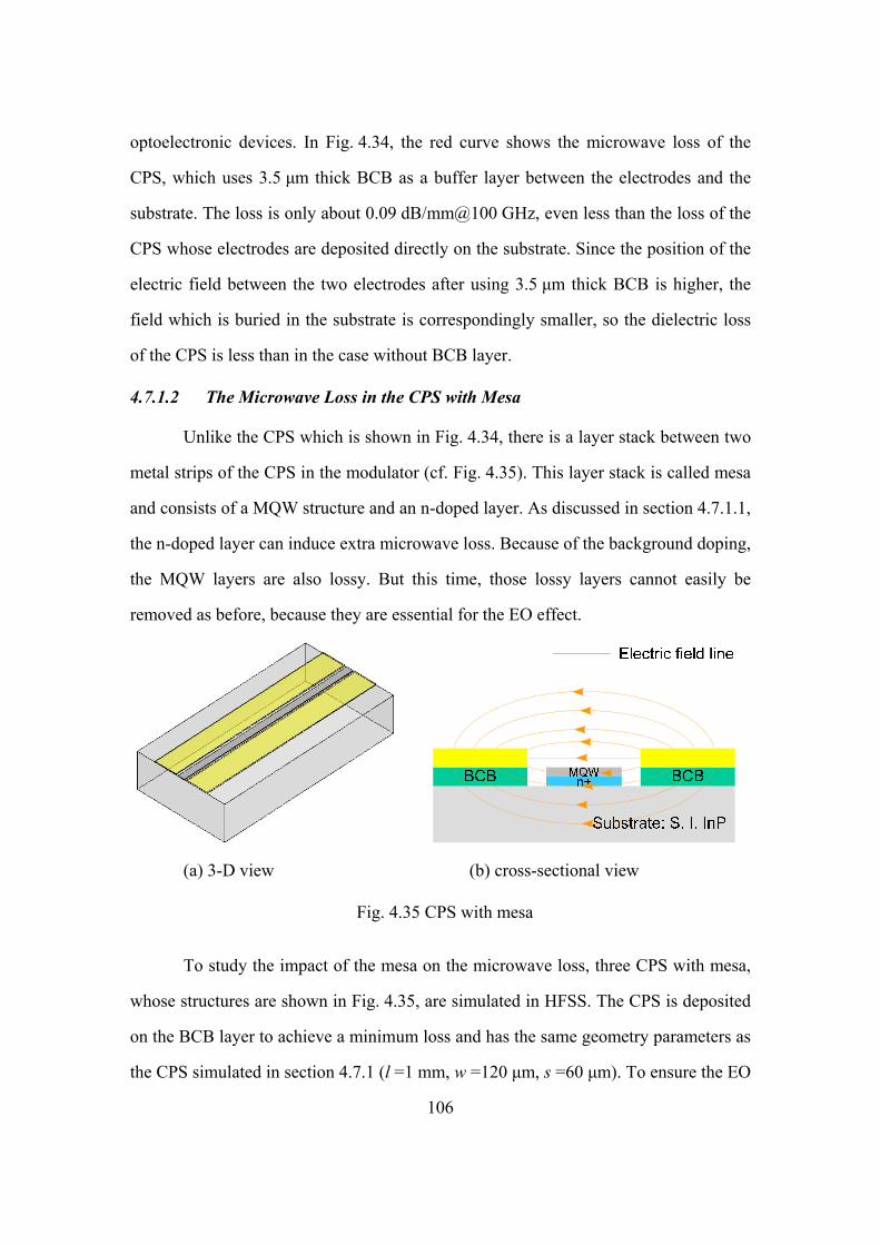
106
optoelectronic devices. In Fig. 4.34, the red curve shows the microwave loss of the
CPS, which uses 3.5 μm thick BCB as a buffer layer between the electrodes and the
substrate. The loss is only about 0.09 dB/mm@100 GHz, even less than the loss of the
CPS whose electrodes are deposited directly on the substrate. Since the position of the
electric field between the two electrodes after using 3.5 μm thick BCB is higher, the
field which is buried in the substrate is correspondingly smaller, so the dielectric loss
of the CPS is less than in the case without BCB layer.
4.7.1.2 The Microwave Loss in the CPS with Mesa
Unlike the CPS which is shown in Fig. 4.34, there is a layer stack between two
metal strips of the CPS in the modulator (cf. Fig. 4.35). This layer stack is called mesa
and consists of a MQW structure and an n-doped layer. As discussed in section 4.7.1.1,
the n-doped layer can induce extra microwave loss. Because of the background doping,
the MQW layers are also lossy. But this time, those lossy layers cannot easily be
removed as before, because they are essential for the EO effect.
(a) 3-D view (b) cross-sectional view
Fig. 4.35 CPS with mesa
To study the impact of the mesa on the microwave loss, three CPS with mesa,
whose structures are shown in Fig. 4.35, are simulated in HFSS. The CPS is deposited
on the BCB layer to achieve a minimum loss and has the same geometry parameters as
the CPS simulated in section 4.7.1 (l =1 mm, w =120 μm, s =60 μm). To ensure the EO
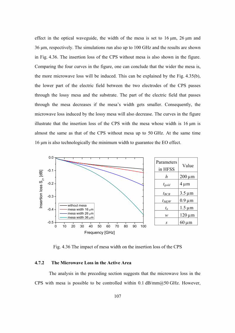
107
effect in the optical waveguide, the width of the mesa is set to 16 μm, 26 μm and
36 μm, respectively. The simulations run also up to 100 GHz and the results are shown
in Fig. 4.36. The insertion loss of the CPS without mesa is also shown in the figure.
Comparing the four curves in the figure, one can conclude that the wider the mesa is,
the more microwave loss will be induced. This can be explained by the Fig. 4.35(b),
the lower part of the electric field between the two electrodes of the CPS passes
through the lossy mesa and the substrate. The part of the electric field that passes
through the mesa decreases if the mesa’s width gets smaller. Consequently, the
microwave loss induced by the lossy mesa will also decrease. The curves in the figure
illustrate that the insertion loss of the CPS with the mesa whose width is 16 μm is
almost the same as that of the CPS without mesa up to 50 GHz. At the same time
16 μm is also technologically the minimum width to guarantee the EO effect.
0 10 20 30 40 50 60 70 80 90 100-0.5
-0.4
-0.3
-0.2
-0.1
0.0
Inse
rtion
loss
S21
[dB]
Frequency [GHz]
without mesa mesa width 16 μm mesa width 26 μm mesa width 36 μm
Parameters in HFSS
Value
h 200 μmtgold 4 μm
tBCB 3.5 μm tMQW 0.9 μm
tn 1.5 μm w 120 μms 60 μm
Fig. 4.36 The impact of mesa width on the insertion loss of the CPS
4.7.2 The Microwave Loss in the Active Area
The analysis in the preceding section suggests that the microwave loss in the
CPS with mesa is possible to be controlled within 0.1 dB/mm@50 GHz. However,
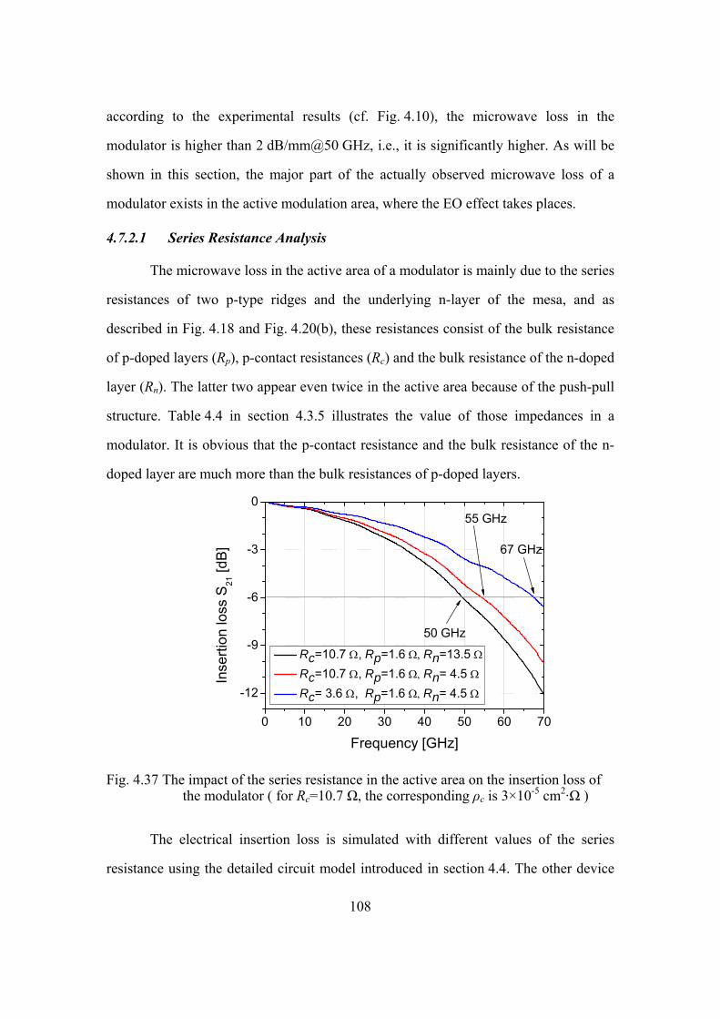
108
according to the experimental results (cf. Fig. 4.10), the microwave loss in the
modulator is higher than 2 dB/mm@50 GHz, i.e., it is significantly higher. As will be
shown in this section, the major part of the actually observed microwave loss of a
modulator exists in the active modulation area, where the EO effect takes places.
4.7.2.1 Series Resistance Analysis
The microwave loss in the active area of a modulator is mainly due to the series
resistances of two p-type ridges and the underlying n-layer of the mesa, and as
described in Fig. 4.18 and Fig. 4.20(b), these resistances consist of the bulk resistance
of p-doped layers (Rp), p-contact resistances (Rc) and the bulk resistance of the n-doped
layer (Rn). The latter two appear even twice in the active area because of the push-pull
structure. Table 4.4 in section 4.3.5 illustrates the value of those impedances in a
modulator. It is obvious that the p-contact resistance and the bulk resistance of the n-
doped layer are much more than the bulk resistances of p-doped layers.
0 10 20 30 40 50 60 70
-12
-9
-6
-3
055 GHz
67 GHz
Inse
rtion
loss
S21
[dB
]
Frequency [GHz]
Rc=10.7 Ω, Rp=1.6 Ω, Rn=13.5 Ω Rc=10.7 Ω, Rp=1.6 Ω, Rn= 4.5 Ω Rc= 3.6 Ω, Rp=1.6 Ω, Rn= 4.5 Ω
50 GHz
Fig. 4.37 The impact of the series resistance in the active area on the insertion loss of the modulator ( for Rc=10.7 Ω, the corresponding ρc is 3×10⁻⁵ cm2·Ω )
The electrical insertion loss is simulated with different values of the series
resistance using the detailed circuit model introduced in section 4.4. The other device
109
parameters are the same as the modulator simulated in Fig. 4.22(a), i.e. l=3 mm,
Λ=250 μm, η= 0.4. The simulation results are shown in Fig. 4.37. The figure shows:
when Rn decreases to one third of its initial value, the electrical bandwidth expands
from 50 GHz to 55 GHz; on this condition, if Rc decreases also to one third of its initial
value, the bandwidth will expand further to 67 GHz. Therefore, it can be concluded
these series resistances are the dominant factor of the microwave loss in a modulator.
On the premise that the EO effect in the modulator is guaranteed, minimizing these
impedance is the most efficient way to expand the working bandwidth of the
modulator.
After analyzing each parameter in the expression (4.3.7), we find it is possible
to decrease Rn to one third. Mathematically, to decrease Rn, one can either decrease d
or increase σn, η, Λ or dn. However, changing one or some of these parameters can
cause other problems. The center to center distance between the two inner electrodes,
d, is also the distance between two optical waveguides, which is an important
parameter for the Y-branch and MMI design. The Y-branch and MMI need redesign if
d changes. The value of the conductivity of the n-layer, σp, is proportional to the
doping density of the n-layer which involves the EO effect. Bigger σn means higher
doping density, which is technologically difficult to achieve. The fill factor η involves
the driving voltage and velocity match and is consequently fixed for the best velocity
match. The period length Λ is tunable, but its maximum is limited by the Bragg
frequency. However it indicates the period length should be designed as long as
possible to achieve a possible small Rn. The thickness of the n-layer dn, is also a
tunable parameter. There is no foreseeable destructive effect after increasing its value
if BCB layer is used as buffer layer instead of n-layer and i-layer for the CPS.
Therefore we increase dn from 0.5 μm to 1.5 μm to decrease Rn to one third.
The p-contact resistance, Rc, can also be reduced and will be discussed
separately in the next section.
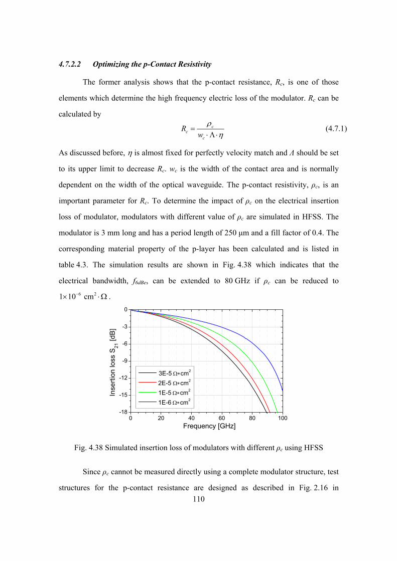
110
4.7.2.2 Optimizing the p-Contact Resistivity
The former analysis shows that the p-contact resistance, Rc, is one of those
elements which determine the high frequency electric loss of the modulator. Rc can be
calculated by
cc
c
Rw
ρη
=⋅Λ ⋅
(4.7.1)
As discussed before, η is almost fixed for perfectly velocity match and Λ should be set
to its upper limit to decrease Rc. wc is the width of the contact area and is normally
dependent on the width of the optical waveguide. The p-contact resistivity, ρc, is an
important parameter for Rc. To determine the impact of ρc on the electrical insertion
loss of modulator, modulators with different value of ρc are simulated in HFSS. The
modulator is 3 mm long and has a period length of 250 μm and a fill factor of 0.4. The
corresponding material property of the p-layer has been calculated and is listed in
table 4.3. The simulation results are shown in Fig. 4.38 which indicates that the
electrical bandwidth, f6dBe, can be extended to 80 GHz if ρc can be reduced to 6 21 10 cm−× ⋅Ω .
0 20 40 60 80 100-18
-15
-12
-9
-6
-3
0
Inse
rtion
loss
S21
[dB]
Frequency [GHz]
3E-5 Ω∗cm2
2E-5 Ω∗cm2
1E-5 Ω∗cm2
1E-6 Ω∗cm2
Fig. 4.38 Simulated insertion loss of modulators with different ρc using HFSS
Since ρc cannot be measured directly using a complete modulator structure, test
structures for the p-contact resistance are designed as described in Fig. 2.16 in
111
section 2.5 and fabricated on the same wafer with modulators to monitor the p-contact
resistivity in the device.
To achieve a small ρc , the top p-layer in the modulator has been heavily doped,
the doping density is 1×1019cm-3. The Ti-Pt-Au alloy has also been used to decrease ρc.
Nevertheless, the measurement shows the p-contact resistivity is around 3×10⁻⁵ Ω·cm2
in the modulator.
The study indicates one can improve ρc by using the post-doping process, by
which the doping density of the top p-layer can be further increased. Our measured
data show that ρc can be improved to 5×10⁻⁶ cm2·Ω in the test structure.
4.7.3 Simulation Results of Optimized Modulator
As discussed above, to minimize the microwave loss in the modulator, the CPS
electrodes should be deposited on the BCB layer, the width of the mesa should shrink,
post Zn-doping process should be used for achieving a smaller p-contact resistivity, the
n-doped layer should be designed thicker and the center-to-center distance between
two ridges should be as short as possible.
To study the effect of those parameters on the electro-optical response, three
groups of modulators are simulated in HFSS. All of those modulators use the BCB
layer as a buffer layer between the CPS electrodes and the substrate. The TWE length
of all modulators is 3 mm. For each group of modulator, the fill factor increases from
0.2 to 0.7 linearly. All of the simulated electrical insertion loss are further converted
into electro-optical response using (3.4.16). The nopt used in the calculation is set as
3.7. The modulators of group one have the p-contact resistivity (ρc) of 2×10⁻⁵ Ω·cm2,
the mesa width (wmesa)of 26 μm, the center-to-center distance between two ridges (d)
of 13 μm, the ridge width (wwg) of 2.8 μm (These parameters are shown in Fig. 3.13).
The modulators of group two have the same parameters as the group one except a
better p-contact resistivity (ρc) of 5×10⁻⁶ Ω·cm2. The modulators of group three have
also a better p-contact resistivity of 5×10⁻⁶ Ω·cm2, the same as that of type two, but the
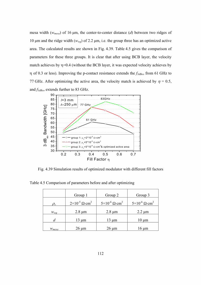
112
mesa width (wmesa) of 16 μm, the center-to-center distance (d) between two ridges of
10 μm and the ridge width (wwg) of 2.2 μm, i.e. the group three has an optimized active
area. The calculated results are shown in Fig. 4.39. Table 4.5 gives the comparison of
parameters for these three groups. It is clear that after using BCB layer, the velocity
match achieves by η=0.4 (without the BCB layer, it was expected velocity achieves by
η of 0.3 or less). Improving the p-contact resistance extends the f3dBeo from 61 GHz to
77 GHz. After optimizing the active area, the velocity match is achieved by η = 0.5,
and f3dBeo extends further to 83 GHz.
0.2 0.3 0.4 0.5 0.6 0.730354045505560657075808590
group 1: ρc=2*10-5 Ω -cm2
group 2: ρc=5*10-6 Ω -cm2
group 3: ρc=5*10-6 Ω -cm2& optimized active area
83GHz
Fill Factor η
3 dB
eo B
andw
idth
[GH
z]
l=3 mm Λ=250 μm 77 GHz
61 GHz
Fig. 4.39 Simulation results of optimized modulator with different fill factors
Table 4.5 Comparison of parameters before and after optimizing
Group 1 Group 2 Group 3
ρc 2×10⁻⁵ Ω·cm2 5×10⁻⁶ Ω·cm2 5×10⁻⁶ Ω·cm2
wwg 2.8 μm 2.8 μm 2.2 μm
d 13 μm 13 μm 10 μm
wmesa 26 μm 26 μm 16 μm
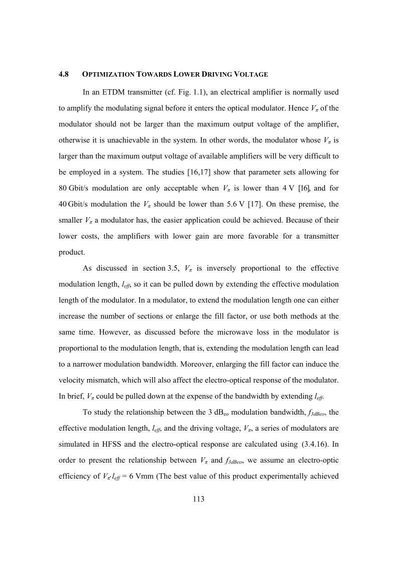
113
4.8 OPTIMIZATION TOWARDS LOWER DRIVING VOLTAGE
In an ETDM transmitter (cf. Fig. 1.1), an electrical amplifier is normally used
to amplify the modulating signal before it enters the optical modulator. Hence Vπ of the
modulator should not be larger than the maximum output voltage of the amplifier,
otherwise it is unachievable in the system. In other words, the modulator whose Vπ is
larger than the maximum output voltage of available amplifiers will be very difficult to
be employed in a system. The studies [16,17] show that parameter sets allowing for
80 Gbit/s modulation are only acceptable when Vπ is lower than 4 V [16], and for
40 Gbit/s modulation the Vπ should be lower than 5.6 V [17]. On these premise, the
smaller Vπ a modulator has, the easier application could be achieved. Because of their
lower costs, the amplifiers with lower gain are more favorable for a transmitter
product.
As discussed in section 3.5, Vπ is inversely proportional to the effective
modulation length, leff, so it can be pulled down by extending the effective modulation
length of the modulator. In a modulator, to extend the modulation length one can either
increase the number of sections or enlarge the fill factor, or use both methods at the
same time. However, as discussed before the microwave loss in the modulator is
proportional to the modulation length, that is, extending the modulation length can lead
to a narrower modulation bandwidth. Moreover, enlarging the fill factor can induce the
velocity mismatch, which will also affect the electro-optical response of the modulator.
In brief, Vπ could be pulled down at the expense of the bandwidth by extending leff.
To study the relationship between the 3 dBeo modulation bandwidth, f3dBeo, the
effective modulation length, leff, and the driving voltage, Vπ, a series of modulators are
simulated in HFSS and the electro-optical response are calculated using (3.4.16). In
order to present the relationship between Vπ and f3dBeo, we assume an electro-optic
efficiency of Vπ⋅leff = 6 Vmm (The best value of this product experimentally achieved
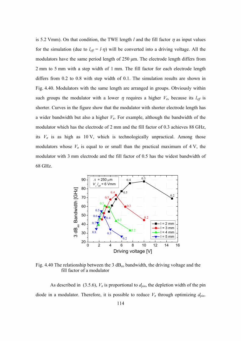
114
is 5.2 Vmm). On that condition, the TWE length l and the fill factor η as input values
for the simulation (due to leff = l⋅η) will be converted into a driving voltage. All the
modulators have the same period length of 250 μm. The electrode length differs from
2 mm to 5 mm with a step width of 1 mm. The fill factor for each electrode length
differs from 0.2 to 0.8 with step width of 0.1. The simulation results are shown in
Fig. 4.40. Modulators with the same length are arranged in groups. Obviously within
such groups the modulator with a lower η requires a higher Vπ, because its leff is
shorter. Curves in the figure show that the modulator with shorter electrode length has
a wider bandwidth but also a higher Vπ. For example, although the bandwidth of the
modulator which has the electrode of 2 mm and the fill factor of 0.3 achieves 88 GHz,
its Vπ is as high as 10 V, which is technologically unpractical. Among those
modulators whose Vπ is equal to or small than the practical maximum of 4 V, the
modulator with 3 mm electrode and the fill factor of 0.5 has the widest bandwidth of
68 GHz.
0 2 4 6 8 10 12 14 1620
30
40
50
60
70
80
90
0.5
0.5
0.4
0.4
0.3
0.3
0.2
0.2
0.3
0.5
0.6
0.7
0.5
0.4 0.3
0.2
0.8
l = 2 mm l = 3 mm l = 4 mm l = 5 mm3
dBeo
Ban
dwid
th [G
Hz]
Driving voltage [V]
Λ = 250 μm V
π l
eff = 6 Vmm
0.2
Fig. 4.40 The relationship between the 3 dBeo bandwidth, the driving voltage and the fill factor of a modulator
As described in (3.5.6), Vπ is proportional to dpin, the depletion width of the pin
diode in a modulator. Therefore, it is possible to reduce Vπ through optimizing dpin.
115
The analysis in section 2.4.2 shows that dpin is the sum of the depletion layer width of
p-type region, xp, the depletion layer width of n-type region, xn, and the thickness of
the i-region, di. Among them, di gives the major contribution. Therefore, if di can be
reduced, Vπ will decrease correspondingly. After analyzing the process of epitaxy, we
find that the thickness cladding layer could be reduced.
Fig 4.41 shows the measured C-V curves of circular pin diodes (will be
discussed in Chapter 6) from wafer MZ-MOD03 and wafer MZ-MOD06. The layer
stack of the wafer MZ-MOD06 has been optimized and the thickness of the i-layer is
250 nm less than that of the wafer MZ-MOD03. The experimental results show that
Cpin of optimized wafer is 25% more than before and the calculated (using (2.4.13))
dpin is 250 nm less than before. Fig 4.42 shows the measured Vπ of the same modulator
structure ( l=3 mm, Λ=0.4 ) from two wafers. The measured Vπ decreases from 7 V to
5.6 V.
-10 -9 -8 -7 -6 -5 -4 -3 -2 -1 0 180
100120140160180200220240260280300
MZ-MOD03
MZ-MOD06
Cap
acita
nce
per u
nit a
rea
[pF/
mm
2 ]
Bias [V] -10 -9 -8 -7 -6 -5 -4 -3 -2 -1 0 1
0.3
0.4
0.5
0.6
0.7
0.8
0.9
1.0
1.1
1.2MZ-MOD03
Wid
th o
f the
dep
letio
n re
gion
dpi
n [μm
]
Bias [V]
MZ-MOD06
Fig. 4.41 Measured C-V curves with two different i-region thickness
Fig. 4.41 illustrates that Cpin increases 25% after optimization. This will result
in a bigger CL as described in (4.3.4) and a higher nμ’ as described in (3.3.4), which
will finally lead to the velocity mismatch. However, the above introduced sandwiched
BCB layer can compensate the increased nμ’. As shown in Fig 4.29, the microwave
index of the unloaded CPS decreases from 2.6 to 2.3 after using the BCB buffer layer.
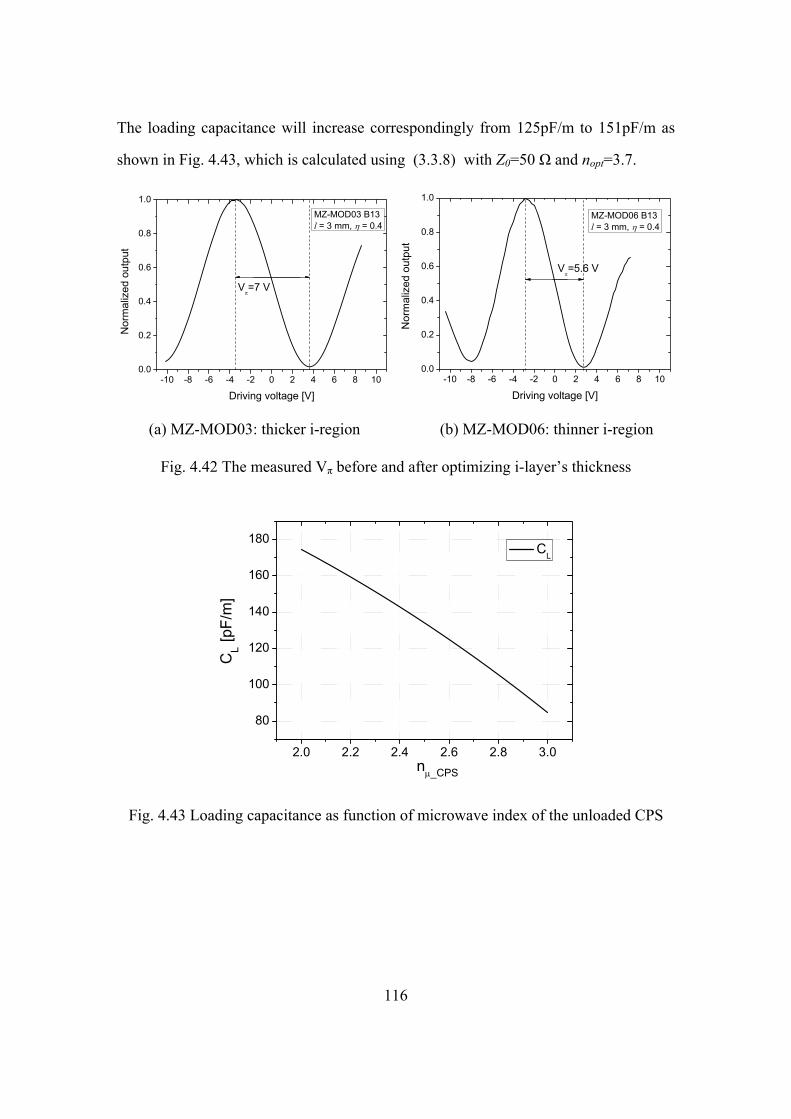
116
The loading capacitance will increase correspondingly from 125pF/m to 151pF/m as
shown in Fig. 4.43, which is calculated using (3.3.8) with Z0=50 Ω and nopt=3.7.
-10 -8 -6 -4 -2 0 2 4 6 8 100.0
0.2
0.4
0.6
0.8
1.0MZ-MOD03 B13l = 3 mm, η = 0.4
Nor
mal
ized
out
put
Driving voltage [V]
Vπ=7 V
-10 -8 -6 -4 -2 0 2 4 6 8 10
0.0
0.2
0.4
0.6
0.8
1.0
Vπ=5.6 V
Nor
mal
ized
out
put
Driving voltage [V]
MZ-MOD06 B13l = 3 mm, η = 0.4
(a) MZ-MOD03: thicker i-region (b) MZ-MOD06: thinner i-region
Fig. 4.42 The measured Vπ before and after optimizing i-layer’s thickness
2.0 2.2 2.4 2.6 2.8 3.0
80
100
120
140
160
180
CL [p
F/m
]
nμ_CPS
CL
Fig. 4.43 Loading capacitance as function of microwave index of the unloaded CPS
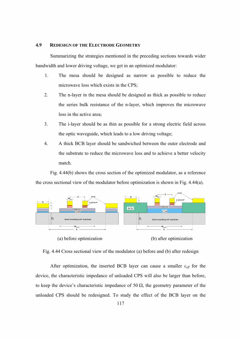
117
4.9 REDESIGN OF THE ELECTRODE GEOMETRY
Summarizing the strategies mentioned in the preceding sections towards wider
bandwidth and lower driving voltage, we get in an optimized modulator:
1. The mesa should be designed as narrow as possible to reduce the
microwave loss which exists in the CPS;
2. The n-layer in the mesa should be designed as thick as possible to reduce
the series bulk resistance of the n-layer, which improves the microwave
loss in the active area;
3. The i-layer should be as thin as possible for a strong electric field across
the optic waveguide, which leads to a low driving voltage;
4. A thick BCB layer should be sandwiched between the outer electrode and
the substrate to reduce the microwave loss and to achieve a better velocity
match.
Fig. 4.44(b) shows the cross section of the optimized modulator, as a reference
the cross sectional view of the modulator before optimization is shown in Fig. 4.44(a).
n+-InP
metal
MQW stack
p-InGaAsP
wwg
w
wmesa
s
Semi-insulating InP substrate
t
h
d
p-InP
n+-InP
metal
MQW stack
p-InGaAsP
wwgw
wmesa
s
Semi-insulating InP substrate
t
h
d
p-InP
BCB
(a) before optimization (b) after optimization
Fig. 4.44 Cross sectional view of the modulator (a) before and (b) after redesign
After optimization, the inserted BCB layer can cause a smaller εeff for the
device, the characteristic impedance of unloaded CPS will also be larger than before,
to keep the device’s characteristic impedance of 50 Ω, the geometry parameter of the
unloaded CPS should be redesigned. To study the effect of the BCB layer on the
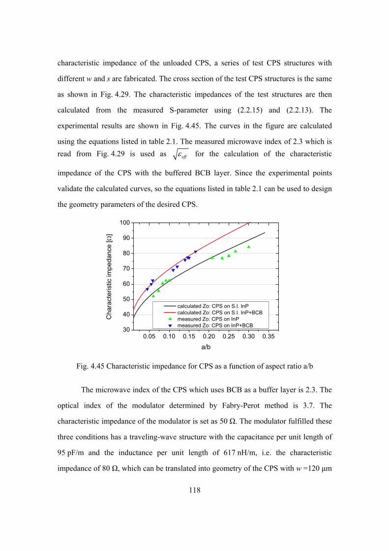
118
characteristic impedance of the unloaded CPS, a series of test CPS structures with
different w and s are fabricated. The cross section of the test CPS structures is the same
as shown in Fig. 4.29. The characteristic impedances of the test structures are then
calculated from the measured S-parameter using (2.2.15) and (2.2.13). The
experimental results are shown in Fig. 4.45. The curves in the figure are calculated
using the equations listed in table 2.1. The measured microwave index of 2.3 which is read from Fig. 4.29 is used as effε for the calculation of the characteristic
impedance of the CPS with the buffered BCB layer. Since the experimental points
validate the calculated curves, so the equations listed in table 2.1 can be used to design
the geometry parameters of the desired CPS.
0.05 0.10 0.15 0.20 0.25 0.30 0.3530
40
50
60
70
80
90
100
Cha
ract
eris
tic im
peda
nce
[Ω]
a/b
calculated Zo: CPS on S.I. InP calculated Zo: CPS on S.I. InP+BCB measured Zo: CPS on InP measured Zo: CPS on InP+BCB
Fig. 4.45 Characteristic impedance for CPS as a function of aspect ratio a/b
The microwave index of the CPS which uses BCB as a buffer layer is 2.3. The
optical index of the modulator determined by Fabry-Perot method is 3.7. The
characteristic impedance of the modulator is set as 50 Ω. The modulator fulfilled these
three conditions has a traveling-wave structure with the capacitance per unit length of
95 pF/m and the inductance per unit length of 617 nH/m, i.e. the characteristic
impedance of 80 Ω, which can be translated into geometry of the CPS with w =120 μm
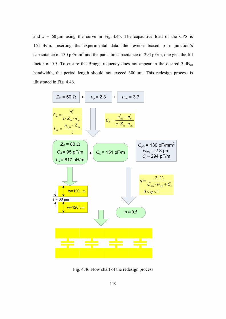
119
and s = 60 μm using the curve in Fig. 4.45. The capacitive load of the CPS is
151 pF/m. Inserting the experimental data: the reverse biased p-i-n junction’s
capacitance of 130 pF/mm2 and the parasitic capacitance of 294 pF/m, one gets the fill
factor of 0.5. To ensure the Bragg frequency does not appear in the desired 3 dBeo
bandwidth, the period length should not exceed 300 μm. This redesign process is
illustrated in Fig. 4.46.
Zm = 50 Ω nμ = 2.3 nopt = 3.7+ +
Z0 = 80 Ω
C0 = 95 pF/m
L0 = 617 nH/m
CL = 151 pF/m+
2
0μ=
⋅ ⋅m opt
nC
c Z n2 2
μ−=
⋅ ⋅opt
Lm opt
n nC
c Z n0
⋅= opt mn Z
Lc
2
0 1
L
pin wg s
CC w C
η
η
⋅=
⋅ +
< <
s = 60 μm
w=120 μm
w=120 μm
Cpin = 130 pF/mm2
wwg = 2.8 μmCs = 294 pF/m
0.5η ≈
Fig. 4.46 Flow chart of the redesign process
120
REFERENCES
[1] “User’s guide of HFSS v9”, Ansoft
[2] S. M. Sze, “Semiconductor devices: physics and technology”, Wiley, New York (1985)
[3] S. L. Chuang, “Physics of optoelectronic devices”, Wiley, (1995)
[4] S. Adachi, “Physical properties of III-V semiconductor compounds: InP, InAs, GaAs, GaP, InGaAs, and InGaAsP”, Wiley (1992)
[5] W. Walukiewicz, “Electron mobility and free-carrier absorption in InP; determination of the compensation ratio”, J. Appl. Phys. 51(5), (1980)
[6] W. Walukiewicz, “Electron mobility and free-carrier absorption in GaAs: determination of the compensation ratio”, J. Appl. Phys. 50(2), (1979)
[7] H. Klein, “Vergleichende Analyse elektrooptischer Effekte in Multi-Quantenfilm- und Bulk-Schichten zur Realisierung von InP-Mach-Zehnder-Modulatoren für 40 Gbit/s”, Diplomarbeit, TU-Berlin (2004)
[8] K. Chang, “Handbook of optical components and engineering”, Wiley, Hoboken, NJ (2003)
[9] S. L. March, “Simple equations characterize bond wires”, Microwave & RF, Nov., 105-110 (1991)
[10] David M. Pozar, “Microwave engineering”, 3rd Ed., Wiley (2005)
[11] M. J. W. Rodwell, S. T. Allen, R. Y. Yu, M.G. Case, U. Bhattacharya, M. Reddy, E. Carman, M Kamegawa, Y. Konishi, J. Pusl and R. Pullela: “Active and nonlinear wave propagation devices in ultrafast electronics and optoelectronics,” Proc. IEEE 82, 1037-1059 (1994)
[12] H. Chen, H. N. Klein, D. Hoffmann, K.-O. Velthaus and H. Venghaus, “Improvement strategy towards 80 Gbit/s low drive voltage InP based Mach-Zehnder modulator”, Proceed. 4th joint symposium on opto- and microelectronic devices and circuits, SODC2006 85-89 (2006)
[13] R. G. Walker: “High-Speed III-V Semiconductor Intensity Modulators,” IEEE J. Quantum Electron. 27, 654-667 (1991)
[14] E. Voges and K. Petermann, “Optische Kommunikationstechnik”, Springer, Berlin (2002)
[15] R. Spickermann, S. R. Sakamoto and N. Dagli, “In traveling wave modulators which velocity to match?”, Lasers and Electro-Optics Society Annual Meeting, 1996. LEOS 96., IEEE 2, 97-98 (1996)
121
[16] W. S. Lee: “80+ Gbit/s ETDM system implementation: an overview of current technologies,” Opt. Fiber Commun. Conf. OFC2006, paper OTuB3
[17] Datasheet of SHF product, 803P, Rev. 3.0, (2004)

122
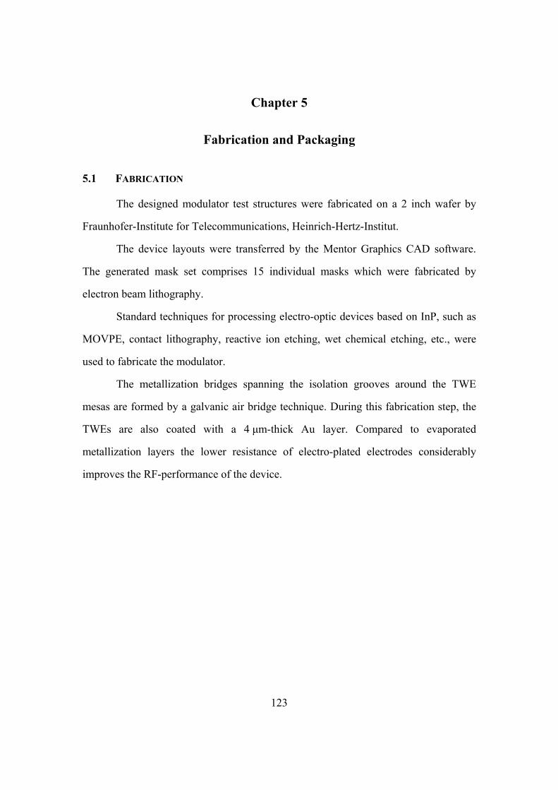
123
Chapter 5
Fabrication and Packaging
5.1 FABRICATION
The designed modulator test structures were fabricated on a 2 inch wafer by
Fraunhofer-Institute for Telecommunications, Heinrich-Hertz-Institut.
The device layouts were transferred by the Mentor Graphics CAD software.
The generated mask set comprises 15 individual masks which were fabricated by
electron beam lithography.
Standard techniques for processing electro-optic devices based on InP, such as
MOVPE, contact lithography, reactive ion etching, wet chemical etching, etc., were
used to fabricate the modulator.
The metallization bridges spanning the isolation grooves around the TWE
mesas are formed by a galvanic air bridge technique. During this fabrication step, the
TWEs are also coated with a 4 μm-thick Au layer. Compared to evaporated
metallization layers the lower resistance of electro-plated electrodes considerably
improves the RF-performance of the device.
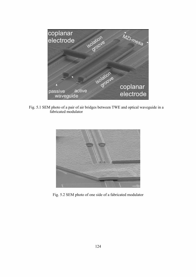
124
MZI-mesa
isolation
groove
isolation
groove
coplanarelectrodewaveguide
activepassive
coplanarelectrode
Fig. 5.1 SEM photo of a pair of air bridges between TWE and optical waveguide in a fabricated modulator
Fig. 5.2 SEM photo of one side of a fabricated modulator
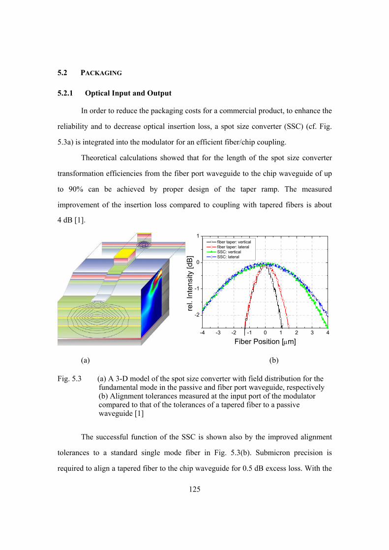
125
5.2 PACKAGING
5.2.1 Optical Input and Output
In order to reduce the packaging costs for a commercial product, to enhance the
reliability and to decrease optical insertion loss, a spot size converter (SSC) (cf. Fig.
5.3a) is integrated into the modulator for an efficient fiber/chip coupling.
Theoretical calculations showed that for the length of the spot size converter
transformation efficiencies from the fiber port waveguide to the chip waveguide of up
to 90% can be achieved by proper design of the taper ramp. The measured
improvement of the insertion loss compared to coupling with tapered fibers is about
4 dB [1].
-4 -3 -2 -1 0 1 2 3 4
-2
-1
0
1 fiber taper: vertical fiber taper: lateral SSC: vertical SSC: lateral
rel.
Inte
nsity
[dB]
Fiber Position [μm]
(a) (b)
Fig. 5.3 (a) A 3-D model of the spot size converter with field distribution for the fundamental mode in the passive and fiber port waveguide, respectively (b) Alignment tolerances measured at the input port of the modulator compared to that of the tolerances of a tapered fiber to a passive waveguide [1]
The successful function of the SSC is shown also by the improved alignment
tolerances to a standard single mode fiber in Fig. 5.3(b). Submicron precision is
required to align a tapered fiber to the chip waveguide for 0.5 dB excess loss. With the
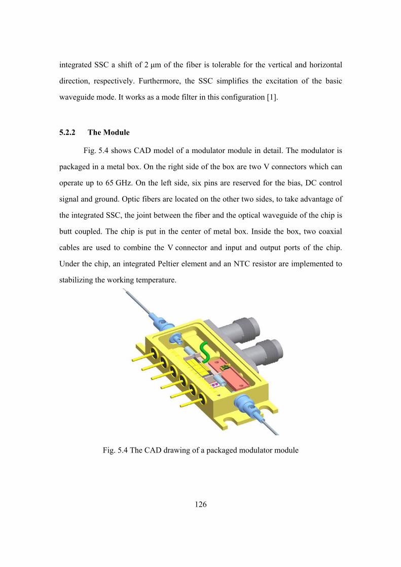
126
integrated SSC a shift of 2 μm of the fiber is tolerable for the vertical and horizontal
direction, respectively. Furthermore, the SSC simplifies the excitation of the basic
waveguide mode. It works as a mode filter in this configuration [1].
5.2.2 The Module
Fig. 5.4 shows CAD model of a modulator module in detail. The modulator is
packaged in a metal box. On the right side of the box are two V connectors which can
operate up to 65 GHz. On the left side, six pins are reserved for the bias, DC control
signal and ground. Optic fibers are located on the other two sides, to take advantage of
the integrated SSC, the joint between the fiber and the optical waveguide of the chip is
butt coupled. The chip is put in the center of metal box. Inside the box, two coaxial
cables are used to combine the V connector and input and output ports of the chip.
Under the chip, an integrated Peltier element and an NTC resistor are implemented to
stabilizing the working temperature.
Fig. 5.4 The CAD drawing of a packaged modulator module
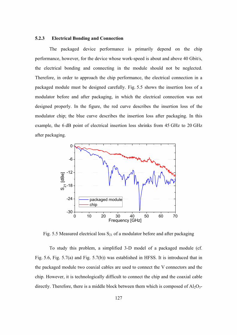
127
5.2.3 Electrical Bonding and Connection
The packaged device performance is primarily depend on the chip
performance, however, for the device whose work-speed is about and above 40 Gbit/s,
the electrical bonding and connecting in the module should not be neglected.
Therefore, in order to approach the chip performance, the electrical connection in a
packaged module must be designed carefully. Fig. 5.5 shows the insertion loss of a
modulator before and after packaging, in which the electrical connection was not
designed properly. In the figure, the red curve describes the insertion loss of the
modulator chip; the blue curve describes the insertion loss after packaging. In this
example, the 6 dB point of electrical insertion loss shrinks from 45 GHz to 20 GHz
after packaging.
0 10 20 30 40 50 60 70-30
-24
-18
-12
-6
0
S 21 [d
Be]
Frequency [GHz]
packaged module chip
Fig. 5.5 Measured electrical loss S21 of a modulator before and after packaging
To study this problem, a simplified 3-D model of a packaged module (cf.
Fig. 5.6, Fig. 5.7(a) and Fig. 5.7(b)) was established in HFSS. It is introduced that in
the packaged module two coaxial cables are used to connect the V connectors and the
chip. However, it is technologically difficult to connect the chip and the coaxial cable
directly. Therefore, there is a middle block between them which is composed of Al2O3-
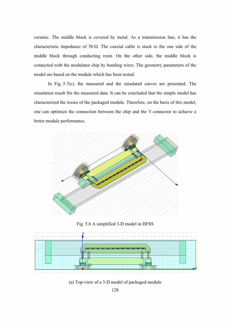
128
ceramic. The middle block is covered by metal. As a transmission line, it has the
characteristic impedance of 50 Ω. The coaxial cable is stuck to the one side of the
middle block through conducting resin. On the other side, the middle block is
connected with the modulator chip by bonding wires. The geometry parameters of the
model are based on the module which has been tested.
In Fig. 5.7(c), the measured and the simulated curves are presented. The
simulation result fits the measured data. It can be concluded that the simple model has
characterized the losses of the packaged module. Therefore, on the basis of this model,
one can optimize the connection between the chip and the V connector to achieve a
better module performance.
Fig. 5.6 A simplified 3-D model in HFSS
(a) Top-view of a 3-D model of packaged module
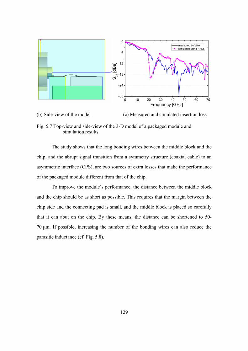
129
0 10 20 30 40 50 60 70-30
-24
-18
-12
-6
0
S21
[dB
e]
Frequency [GHz]
measured by VNA simulated using HFSS
(b) Side-view of the model (c) Measured and simulated insertion loss
Fig. 5.7 Top-view and side-view of the 3-D model of a packaged module and simulation results
The study shows that the long bonding wires between the middle block and the
chip, and the abrupt signal transition from a symmetry structure (coaxial cable) to an
asymmetric interface (CPS), are two sources of extra losses that make the performance
of the packaged module different from that of the chip.
To improve the module’s performance, the distance between the middle block
and the chip should be as short as possible. This requires that the margin between the
chip side and the connecting pad is small, and the middle block is placed so carefully
that it can abut on the chip. By these means, the distance can be shortened to 50-
70 μm. If possible, increasing the number of the bonding wires can also reduce the
parasitic inductance (cf. Fig. 5.8).
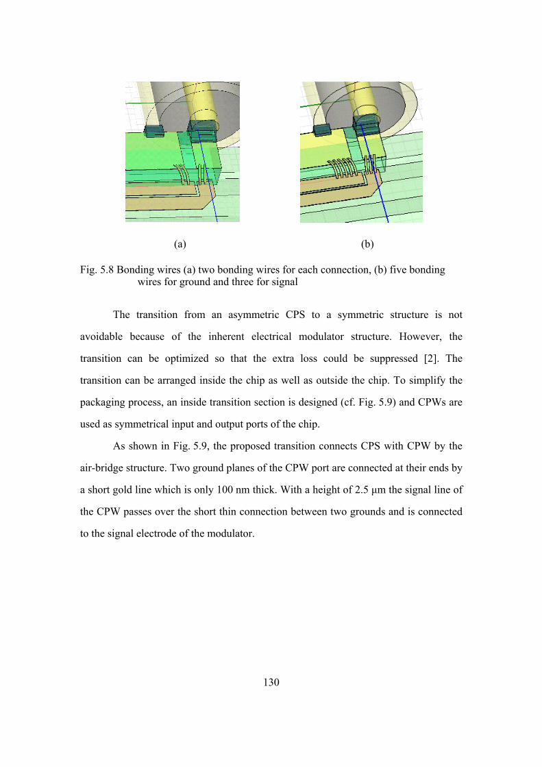
130
(a) (b)
Fig. 5.8 Bonding wires (a) two bonding wires for each connection, (b) five bonding wires for ground and three for signal
The transition from an asymmetric CPS to a symmetric structure is not
avoidable because of the inherent electrical modulator structure. However, the
transition can be optimized so that the extra loss could be suppressed [2]. The
transition can be arranged inside the chip as well as outside the chip. To simplify the
packaging process, an inside transition section is designed (cf. Fig. 5.9) and CPWs are
used as symmetrical input and output ports of the chip.
As shown in Fig. 5.9, the proposed transition connects CPS with CPW by the
air-bridge structure. Two ground planes of the CPW port are connected at their ends by
a short gold line which is only 100 nm thick. With a height of 2.5 μm the signal line of
the CPW passes over the short thin connection between two grounds and is connected
to the signal electrode of the modulator.
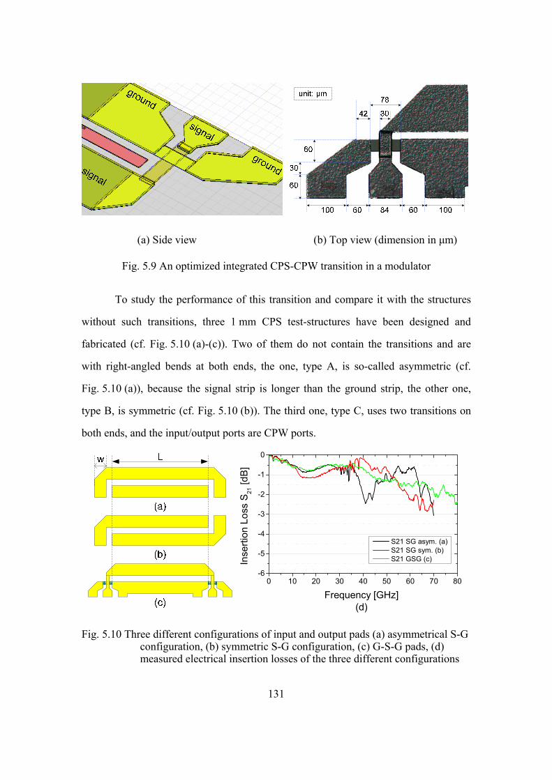
131
(a) Side view (b) Top view (dimension in μm)
Fig. 5.9 An optimized integrated CPS-CPW transition in a modulator
To study the performance of this transition and compare it with the structures
without such transitions, three 1 mm CPS test-structures have been designed and
fabricated (cf. Fig. 5.10 (a)-(c)). Two of them do not contain the transitions and are
with right-angled bends at both ends, the one, type A, is so-called asymmetric (cf.
Fig. 5.10 (a)), because the signal strip is longer than the ground strip, the other one,
type B, is symmetric (cf. Fig. 5.10 (b)). The third one, type C, uses two transitions on
both ends, and the input/output ports are CPW ports.
0 10 20 30 40 50 60 70 80-6
-5
-4
-3
-2
-1
0
Inse
rtion
Los
s S
21 [d
B]
Frequency [GHz](d)
S21 SG asym. (a) S21 SG sym. (b) S21 GSG (c)
Fig. 5.10 Three different configurations of input and output pads (a) asymmetrical S-G configuration, (b) symmetric S-G configuration, (c) G-S-G pads, (d) measured electrical insertion losses of the three different configurations
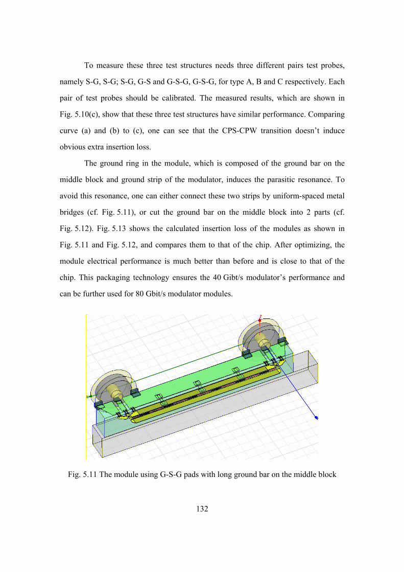
132
To measure these three test structures needs three different pairs test probes,
namely S-G, S-G; S-G, G-S and G-S-G, G-S-G, for type A, B and C respectively. Each
pair of test probes should be calibrated. The measured results, which are shown in
Fig. 5.10(c), show that these three test structures have similar performance. Comparing
curve (a) and (b) to (c), one can see that the CPS-CPW transition doesn’t induce
obvious extra insertion loss.
The ground ring in the module, which is composed of the ground bar on the
middle block and ground strip of the modulator, induces the parasitic resonance. To
avoid this resonance, one can either connect these two strips by uniform-spaced metal
bridges (cf. Fig. 5.11), or cut the ground bar on the middle block into 2 parts (cf.
Fig. 5.12). Fig. 5.13 shows the calculated insertion loss of the modules as shown in
Fig. 5.11 and Fig. 5.12, and compares them to that of the chip. After optimizing, the
module electrical performance is much better than before and is close to that of the
chip. This packaging technology ensures the 40 Gibt/s modulator’s performance and
can be further used for 80 Gbit/s modulator modules.
Fig. 5.11 The module using G-S-G pads with long ground bar on the middle block
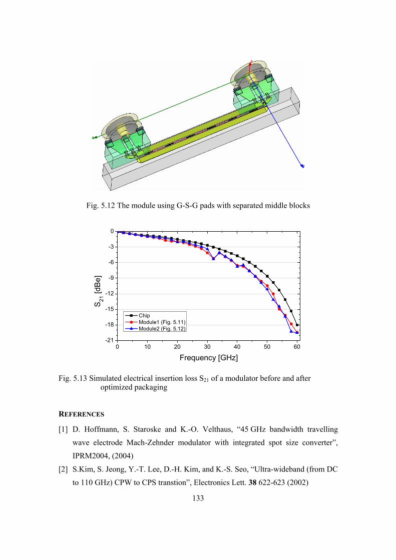
133
Fig. 5.12 The module using G-S-G pads with separated middle blocks
0 10 20 30 40 50 60-21
-18
-15
-12
-9
-6
-3
0
S 21 [d
Be]
Frequency [GHz]
Chip Module1 (Fig. 5.11) Module2 (Fig. 5.12)
Fig. 5.13 Simulated electrical insertion loss S21 of a modulator before and after optimized packaging
REFERENCES
[1] D. Hoffmann, S. Staroske and K.-O. Velthaus, “45 GHz bandwidth travelling
wave electrode Mach-Zehnder modulator with integrated spot size converter”,
IPRM2004, (2004)
[2] S.Kim, S. Jeong, Y.-T. Lee, D.-H. Kim, and K.-S. Seo, “Ultra-wideband (from DC
to 110 GHz) CPW to CPS transtion”, Electronics Lett. 38 622-623 (2002)
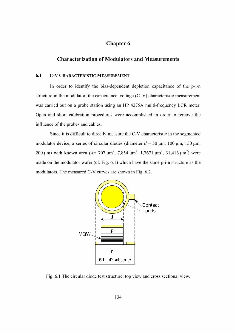
134
Chapter 6
Characterization of Modulators and Measurements
6.1 C-V CHARACTERISTIC MEASUREMENT
In order to identify the bias-dependent depletion capacitance of the p-i-n
structure in the modulator, the capacitance–voltage (C–V) characteristic measurement
was carried out on a probe station using an HP 4275A multi-frequency LCR meter.
Open and short calibration procedures were accomplished in order to remove the
influence of the probes and cables.
Since it is difficult to directly measure the C-V characteristic in the segmented
modulator device, a series of circular diodes (diameter d = 50 μm, 100 μm, 150 μm,
200 μm) with known area (A= 707 μm2, 7,854 μm2, 1,7671 μm2, 31,416 μm2) were
made on the modulator wafer (cf. Fig. 6.1) which have the same p-i-n structure as the
modulators. The measured C-V curves are shown in Fig. 6.2.
Fig. 6.1 The circular diode test structure: top view and cross sectional view.
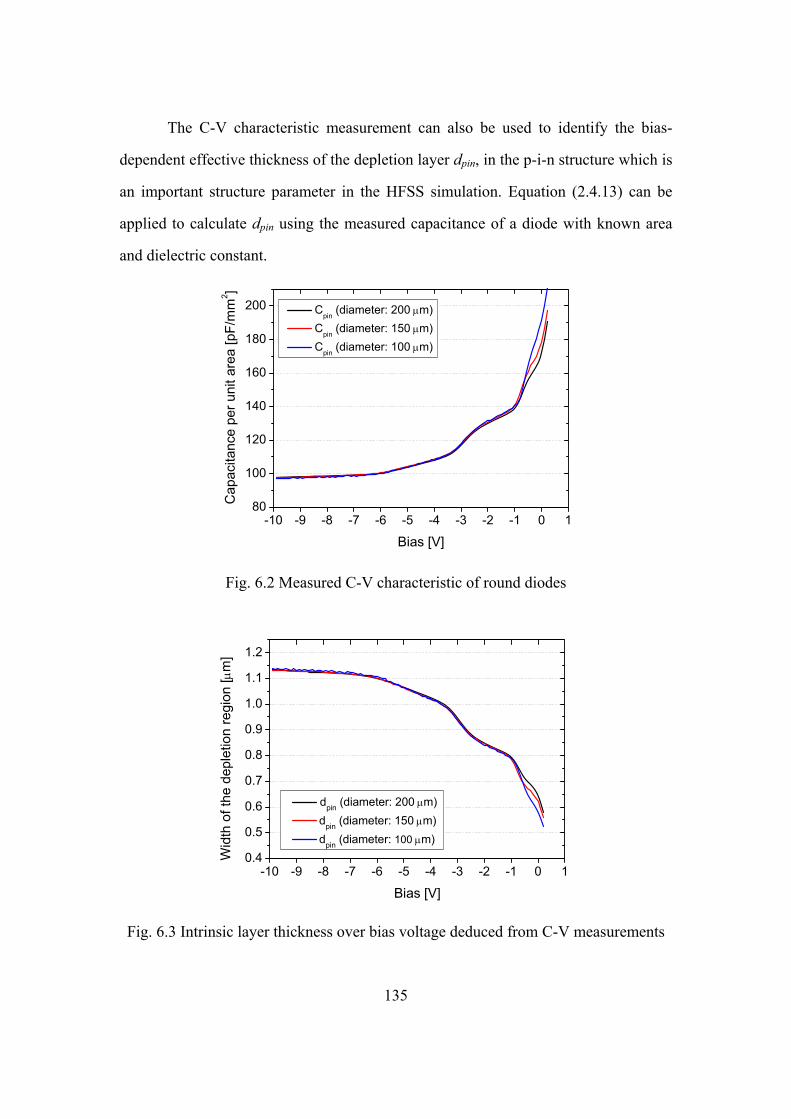
135
The C-V characteristic measurement can also be used to identify the bias-
dependent effective thickness of the depletion layer dpin, in the p-i-n structure which is
an important structure parameter in the HFSS simulation. Equation (2.4.13) can be
applied to calculate dpin using the measured capacitance of a diode with known area
and dielectric constant.
-10 -9 -8 -7 -6 -5 -4 -3 -2 -1 0 180
100
120
140
160
180
200
Cap
acita
nce
per u
nit a
rea
[pF/
mm
2 ]
Bias [V]
Cpin
(diameter: 200 μm) Cpin (diameter: 150 μm) Cpin (diameter: 100 μm)
Fig. 6.2 Measured C-V characteristic of round diodes
-10 -9 -8 -7 -6 -5 -4 -3 -2 -1 0 10.4
0.5
0.6
0.7
0.8
0.9
1.0
1.1
1.2
Wid
th o
f the
dep
letio
n re
gion
[μm
]
Bias [V]
dpin (diameter: 200 μm) dpin (diameter: 150 μm) dpin (diameter: 100 μm)
Fig. 6.3 Intrinsic layer thickness over bias voltage deduced from C-V measurements
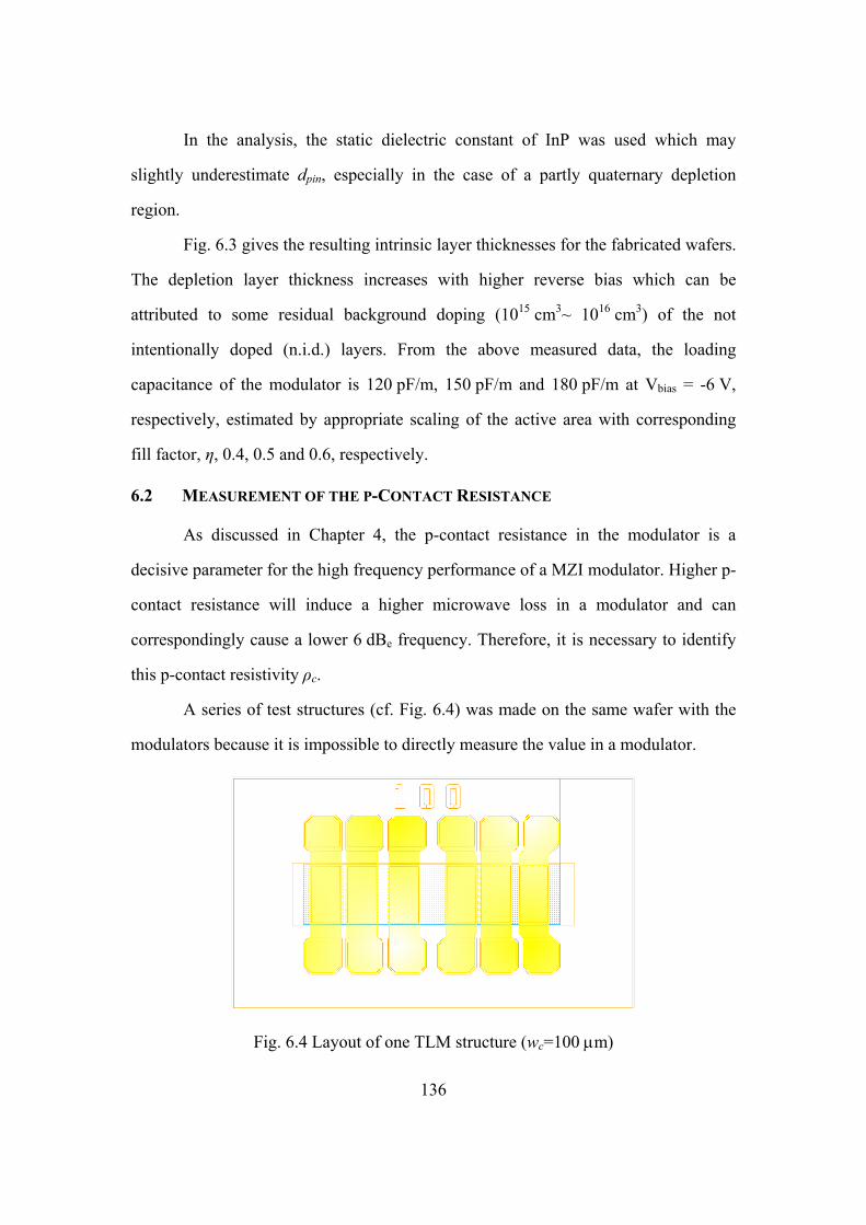
136
In the analysis, the static dielectric constant of InP was used which may
slightly underestimate dpin, especially in the case of a partly quaternary depletion
region.
Fig. 6.3 gives the resulting intrinsic layer thicknesses for the fabricated wafers.
The depletion layer thickness increases with higher reverse bias which can be
attributed to some residual background doping (1015 cm3~ 1016 cm3) of the not
intentionally doped (n.i.d.) layers. From the above measured data, the loading
capacitance of the modulator is 120 pF/m, 150 pF/m and 180 pF/m at Vbias = -6 V,
respectively, estimated by appropriate scaling of the active area with corresponding
fill factor, η, 0.4, 0.5 and 0.6, respectively.
6.2 MEASUREMENT OF THE P-CONTACT RESISTANCE
As discussed in Chapter 4, the p-contact resistance in the modulator is a
decisive parameter for the high frequency performance of a MZI modulator. Higher p-
contact resistance will induce a higher microwave loss in a modulator and can
correspondingly cause a lower 6 dBe frequency. Therefore, it is necessary to identify
this p-contact resistivity ρc.
A series of test structures (cf. Fig. 6.4) was made on the same wafer with the
modulators because it is impossible to directly measure the value in a modulator.
Fig. 6.4 Layout of one TLM structure (wc=100 μm)
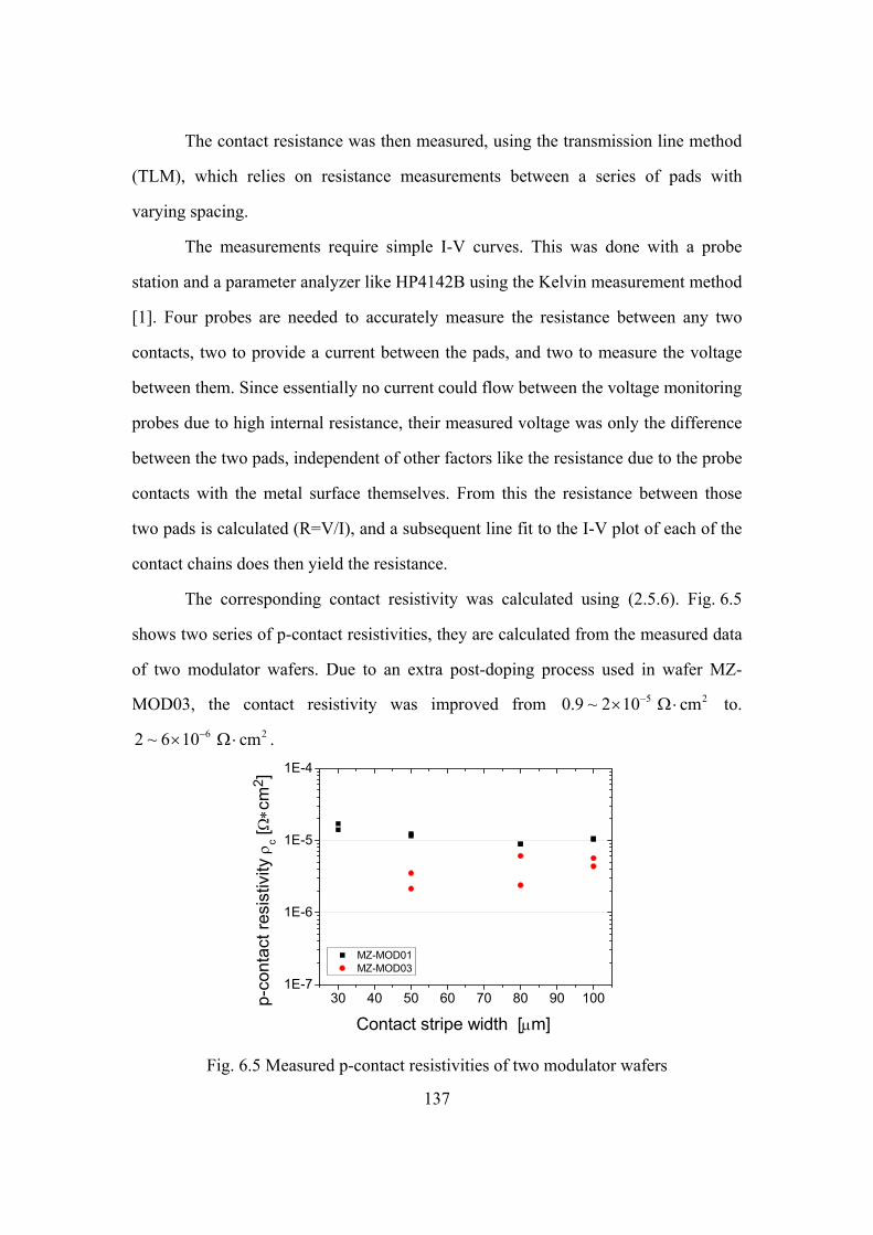
137
The contact resistance was then measured, using the transmission line method
(TLM), which relies on resistance measurements between a series of pads with
varying spacing.
The measurements require simple I-V curves. This was done with a probe
station and a parameter analyzer like HP4142B using the Kelvin measurement method
[1]. Four probes are needed to accurately measure the resistance between any two
contacts, two to provide a current between the pads, and two to measure the voltage
between them. Since essentially no current could flow between the voltage monitoring
probes due to high internal resistance, their measured voltage was only the difference
between the two pads, independent of other factors like the resistance due to the probe
contacts with the metal surface themselves. From this the resistance between those
two pads is calculated (R=V/I), and a subsequent line fit to the I-V plot of each of the
contact chains does then yield the resistance.
The corresponding contact resistivity was calculated using (2.5.6). Fig. 6.5
shows two series of p-contact resistivities, they are calculated from the measured data
of two modulator wafers. Due to an extra post-doping process used in wafer MZ-
MOD03, the contact resistivity was improved from 5 20.9 ~ 2 10 cm−× Ω⋅ to. 6 22 ~ 6 10 cm−× Ω⋅ .
30 40 50 60 70 80 90 1001E-7
1E-6
1E-5
1E-4
MZ-MOD01 MZ-MOD03
p-co
ntac
t res
istiv
ity ρ
c [Ω∗c
m2 ]
Contact stripe width [μm]
Fig. 6.5 Measured p-contact resistivities of two modulator wafers
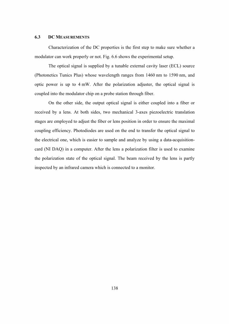
138
6.3 DC MEASUREMENTS
Characterization of the DC properties is the first step to make sure whether a
modulator can work properly or not. Fig. 6.6 shows the experimental setup.
The optical signal is supplied by a tunable external cavity laser (ECL) source
(Photonetics Tunics Plus) whose wavelength ranges from 1460 nm to 1590 nm, and
optic power is up to 4 mW. After the polarization adjuster, the optical signal is
coupled into the modulator chip on a probe station through fiber.
On the other side, the output optical signal is either coupled into a fiber or
received by a lens. At both sides, two mechanical 3-axes piezoelectric translation
stages are employed to adjust the fiber or lens position in order to ensure the maximal
coupling efficiency. Photodiodes are used on the end to transfer the optical signal to
the electrical one, which is easier to sample and analyze by using a data-acquisition-
card (NI DAQ) in a computer. After the lens a polarization filter is used to examine
the polarization state of the optical signal. The beam received by the lens is partly
inspected by an infrared camera which is connected to a monitor.
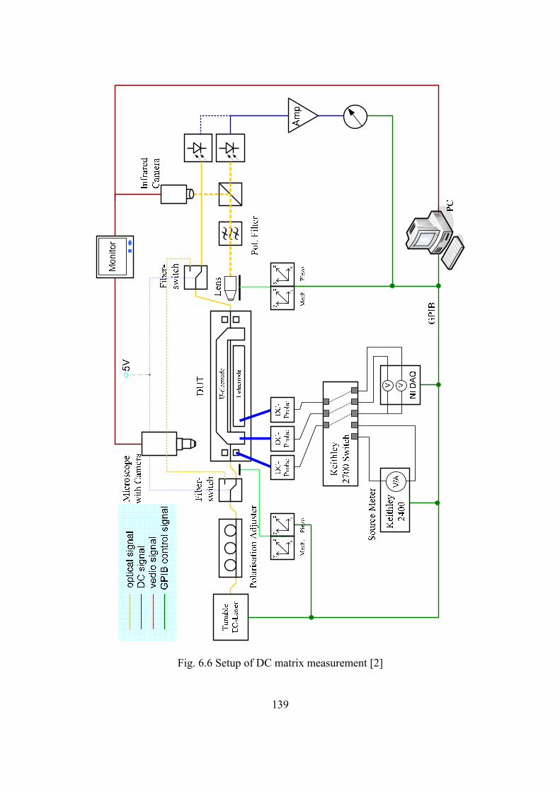
139
Fig. 6.6 Setup of DC matrix measurement [2]
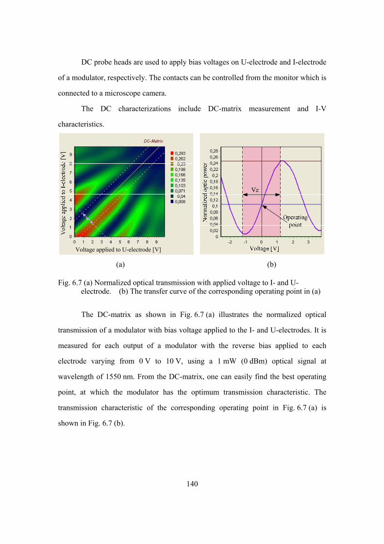
140
DC probe heads are used to apply bias voltages on U-electrode and I-electrode
of a modulator, respectively. The contacts can be controlled from the monitor which is
connected to a microscope camera.
The DC characterizations include DC-matrix measurement and I-V
characteristics.
Voltage applied to U-electrode [V] (a) (b)
Fig. 6.7 (a) Normalized optical transmission with applied voltage to I- and U-electrode. (b) The transfer curve of the corresponding operating point in (a)
The DC-matrix as shown in Fig. 6.7 (a) illustrates the normalized optical
transmission of a modulator with bias voltage applied to the I- and U-electrodes. It is
measured for each output of a modulator with the reverse bias applied to each
electrode varying from 0 V to 10 V, using a 1 mW (0 dBm) optical signal at
wavelength of 1550 nm. From the DC-matrix, one can easily find the best operating
point, at which the modulator has the optimum transmission characteristic. The
transmission characteristic of the corresponding operating point in Fig. 6.7 (a) is
shown in Fig. 6.7 (b).
141
6.4 S-PARAMETER MEASUREMENT
The transmission line properties of the travelling wave electrode Mach-
Zehnder modulator were analyzed on-wafer in the frequency range from 45 MHz to
70 GHz with a vector network analyzer (VNA) HP 8510XF. S-G probe heads were
used for contact at the input and output ports. The SOLT (Short, Open, Load, Thru)
calibration method was used in on-wafer calibration.
The VNA HP 8510XF operates up to 110 GHz, but the frequency range of our
measurement was limited to 70 GHz by the S-G probe heads. As discussed in
Chapter 5, if the new G-S-G pads were integrated in the modulator, the S-parameter
measurement could be extended to 110 GHz, which should be enough for the
characterisation of a 100 Gbit/s modulator.
6.5 ELECTRO-OPTIC MEASUREMENT
Fig. 6.8 shows the experimental setup of the electro-optical small signal
response measurement. The laser signal is provided by an ECL. A polarization
controller is used after ECL in order to ensure the incident light to be TE polarized.
At the input side, the laser signal is coupled into the modulator through a butt
joint. The fiber position is carefully adjusted to transfer maximum light into the
modulator which is placed on a probe station. The electrical modulating signal comes
from an RF signal generator (Agilent E8257D 0-65GHz) and is applied onto the
modulator through an S-G probe. The modulating signal’s power is kept constant at a
level of -7 dBm.
At the output side, the modulated optical signal is coupled into a fiber again
through a butt joint and is amplified by an erbium doped fiber amplifier (EDFA). To
minimize the ASE (amplified spontaneous emission) noise, the EDFA is followed by
a tunable optical bandpass filter. An integrated power meter is used to read out the
optical power. Finally, the modulated optical signal is injected into a photodiode, the
142
output of the photodiode is introduced into an electrical spectrum analyzer (Agilent
E8565EC, frequency ranges from 200 MHz to 50 GHz). Since the frequency range is
limited to 50 GHz by the electrical spectrum analyzer, an external Preselected
Millimeter Mixer (Agilent 11974V, from 50 GHz to 65 GHz) is used to extend the
upper frequency from 50 GHz to 65 GHz which is necessary for the measurement of
an 80 Gbit/s modulator.
Two source meters (Keithley 2400) are employed to provide asymmetric bias
voltages to the modulator. The modulator is electrically terminated with a 50 Ω
resistor.
The test instruments are all controlled by a computer through connected
general purpose interface bus (GPIB) cables. The complicated electro-optical small
signal response measurement is partly automated by a special test program.
143
Fig. 6.8 The setup of electrooptic response measurement (200 MHz – 65 GHz) [3]
144
6.6 SYSTEM MEASUREMENTS
As shown in Fig. 6.9, the 40 Gbit/s eye diagram is measured using an Agilent
86100B oscilloscope with a precision time base (Agilent 86107A) and a dual
70+ GHz electrical remote head (Agilent 86118A). To generate the 231-1 PRBS
(pseudorandom binary sequence) pattern with bit rates of 40 Gbit/s as the input signal
for the module, a pattern generator (SHF BPG 4×11) and a multiplexer (SHF 5005A
4×1) are used together with an electrical amplifier (SHF 804EA).
An optical amplifier (EDFA) at the output of the modulator ensured a constant
optical power level of +7 dBm at 1.55 µm on the high speed photodiode (u2t,
XPDV2020R) when the optical input power on the modulator varies. An optical filter
is used to reduce EDFA-ASE noise.
To measure 80 Gbit/s eye diagrams, an 80 Gbit/s 2:1 multiplexer is inserted
between the 4:1 multiplexer and the electrical amplifier as shown in Fig. 6.10. The
data and data outputs of the 4:1 multiplexer are used as two input data signals for
the 2:1 multiplexer. A 40 GHz clock source is used instead of the 20 GHz one in
40 Gbit/s system measurements.
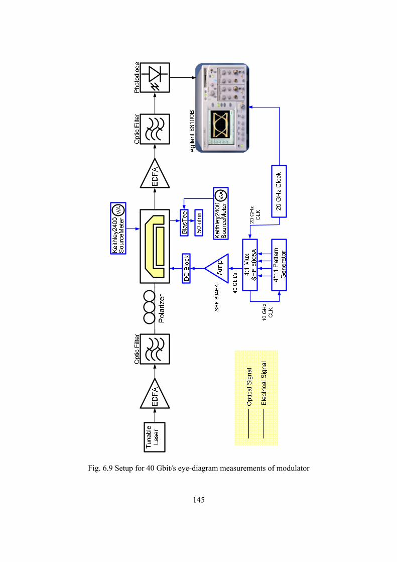
145
Fig. 6.9 Setup for 40 Gbit/s eye-diagram measurements of modulator
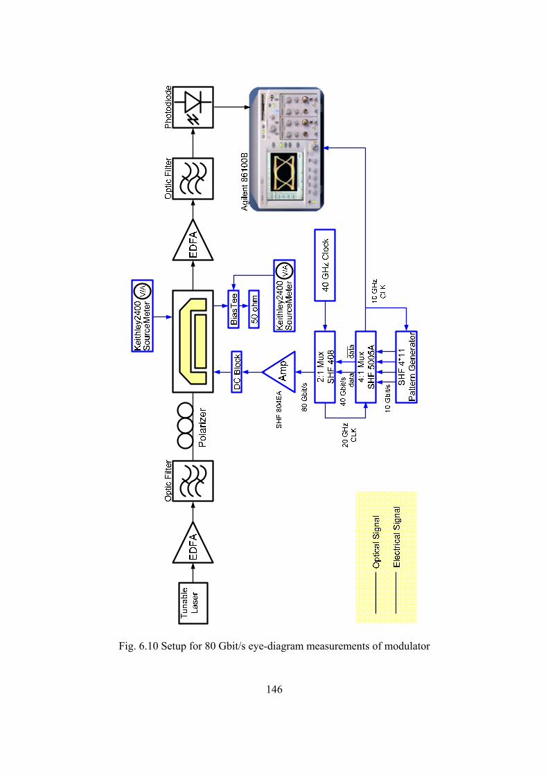
146
Fig. 6.10 Setup for 80 Gbit/s eye-diagram measurements of modulator
147
REFERENCES
[1] D. K. Schroder, “Semiconductor material and device characterization”, 3rd Ed.,
Wiley (2006)
[2] Klein Holger, “Vergleichende Analyse elektrooptischer Effekte in Multi-
Quantenfilm- und Bulk-Schichten zur Realisierung von InP-Mach-Zehnder-
Modulatoren für 40 Gbit/s”, Diplomarbeit, TU-Berlin (2004)
[3] Daniel Kunowski, “Erweiterung und Klassifizierung eines
Hochfrequenzmessplatzes für Mach-Zehnder-Modulatoren bis 65 GHz”,
Diplomarbeit, TFH-Berlin, (2006)
148
Chapter 7
Measured Results and Conclusions
In this chapter, the experimental results of a packaged InP-based MQW TWE
MZM and an InP-based MQW TWE MZM chip are presented. These results show
that the designed InP-based MZI modulators can work properly in 40 Gbit/s optic
communication systems as well as in 80 Gbit/s ones.
7.1 MEASURED RESULTS OF MODULATOR
Due to the continuing optimization work for the high-speed modulator, we
have a few modulators from different wafers which achieved 80 Gbit/s. Some of them
have been packaged, and the newly produced modulators which have exhibited a
better performance will be packaged later.
7.1.1 Measured Results of the First Generation 80 Gbit/s Modulator
A 10 mm long InP based MZI modulator chip (#45 A50) with a TWE
electrode length of 4 mm was packaged into a fiber pigtailed module (cf. Fig. 7.1).
The period length Λ of the modulator is 125 µm, and the active electrode length lE per
period is 62.5 µm. The chip is fixed on a ceramic submount and connected to V-type
RF connectors via semi-rigid coaxial cables. The RF power is fed into the left V-type
RF connector. The right output connector is used for an external 50 Ω terminator. An
integrated Peltier element and an NTC resistor were additionally implemented for
temperature stabilization.
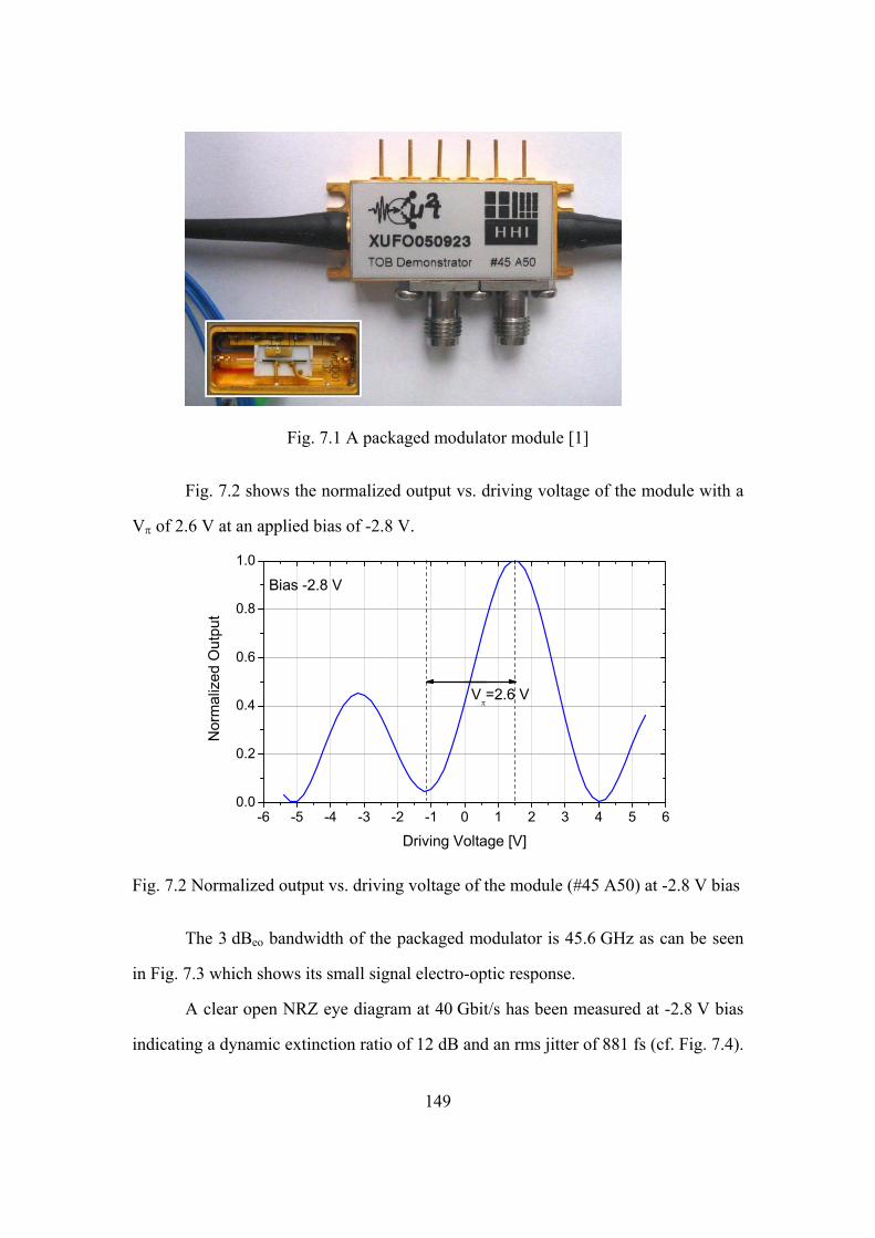
149
Fig. 7.1 A packaged modulator module [1]
Fig. 7.2 shows the normalized output vs. driving voltage of the module with a
Vπ of 2.6 V at an applied bias of -2.8 V.
-6 -5 -4 -3 -2 -1 0 1 2 3 4 5 60.0
0.2
0.4
0.6
0.8
1.0
Nor
mal
ized
Out
put
Driving Voltage [V]
Vπ=2.6 V
Bias -2.8 V
Fig. 7.2 Normalized output vs. driving voltage of the module (#45 A50) at -2.8 V bias
The 3 dBeo bandwidth of the packaged modulator is 45.6 GHz as can be seen
in Fig. 7.3 which shows its small signal electro-optic response.
A clear open NRZ eye diagram at 40 Gbit/s has been measured at -2.8 V bias
indicating a dynamic extinction ratio of 12 dB and an rms jitter of 881 fs (cf. Fig. 7.4).
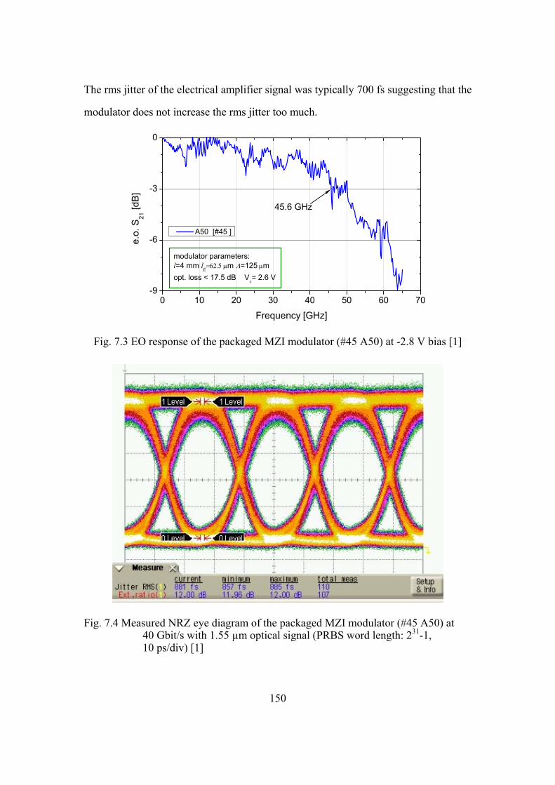
150
The rms jitter of the electrical amplifier signal was typically 700 fs suggesting that the
modulator does not increase the rms jitter too much.
0 10 20 30 40 50 60 70-9
-6
-3
0e.
o. S
21 [d
B]
Frequency [GHz]
A50 [#45 ]
modulator parameters:l=4 mm lE=62.5 μm Λ=125 μmopt. loss < 17.5 dB V
π= 2.6 V
45.6 GHz
Fig. 7.3 EO response of the packaged MZI modulator (#45 A50) at -2.8 V bias [1]
Fig. 7.4 Measured NRZ eye diagram of the packaged MZI modulator (#45 A50) at 40 Gbit/s with 1.55 µm optical signal (PRBS word length: 231-1, 10 ps/div) [1]
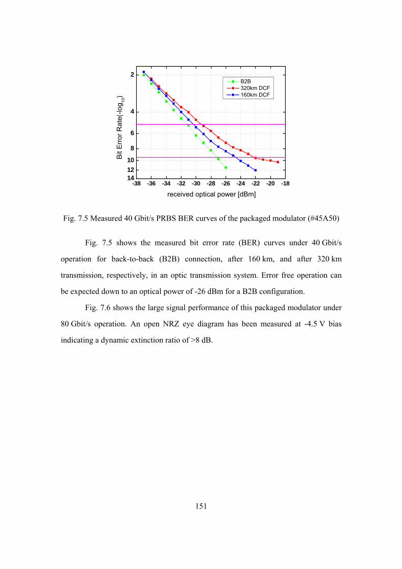
151
2
4
6
8
101214
-38 -36 -34 -32 -30 -28 -26 -24 -22 -20 -18
received optical power [dBm]
Bit
Err
or R
ate(
-log 10
)
B2B 320km DCF 160km DCF
Fig. 7.5 Measured 40 Gbit/s PRBS BER curves of the packaged modulator (#45A50)
Fig. 7.5 shows the measured bit error rate (BER) curves under 40 Gbit/s
operation for back-to-back (B2B) connection, after 160 km, and after 320 km
transmission, respectively, in an optic transmission system. Error free operation can
be expected down to an optical power of -26 dBm for a B2B configuration.
Fig. 7.6 shows the large signal performance of this packaged modulator under
80 Gbit/s operation. An open NRZ eye diagram has been measured at -4.5 V bias
indicating a dynamic extinction ratio of >8 dB.
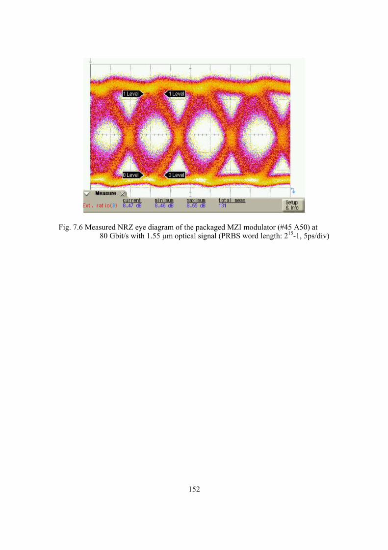
152
Fig. 7.6 Measured NRZ eye diagram of the packaged MZI modulator (#45 A50) at 80 Gbit/s with 1.55 µm optical signal (PRBS word length: 215-1, 5ps/div)
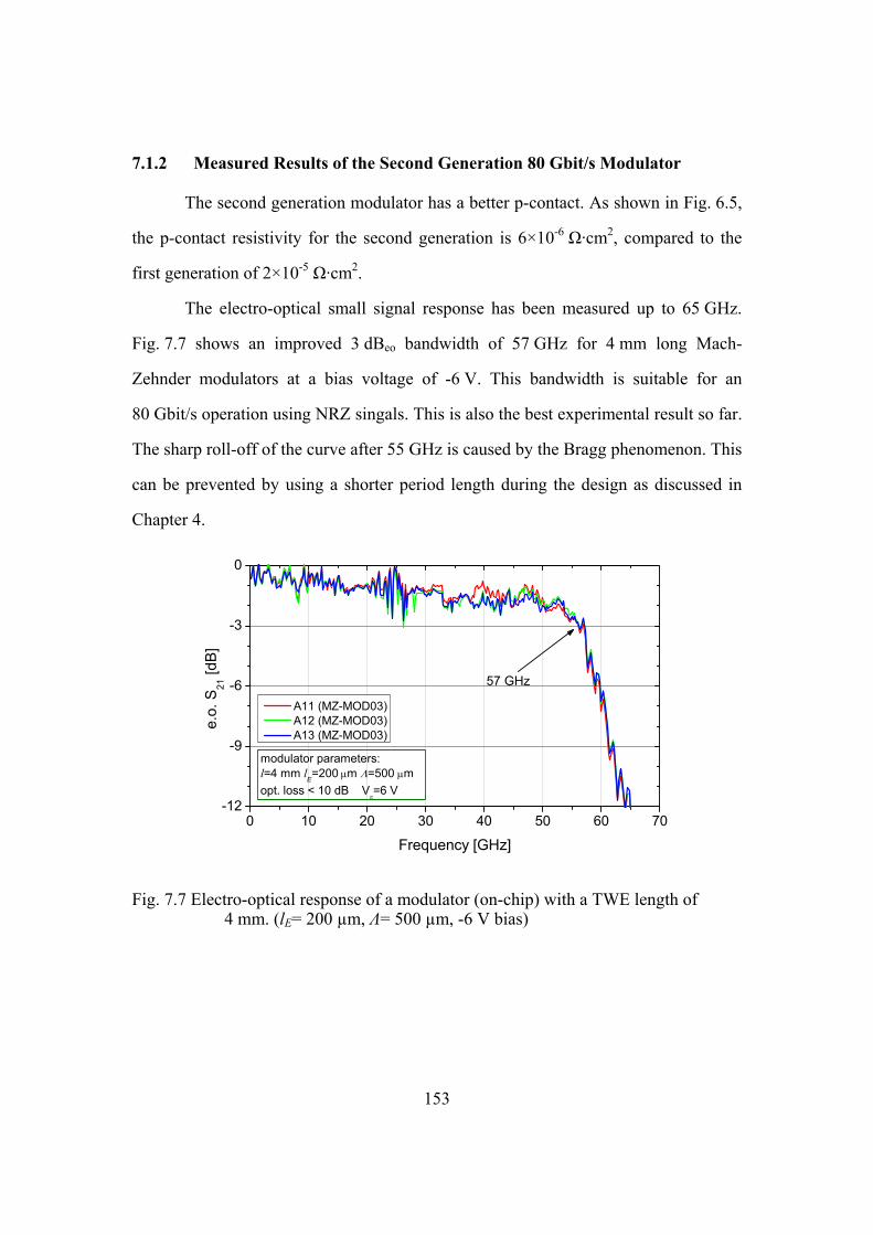
153
7.1.2 Measured Results of the Second Generation 80 Gbit/s Modulator
The second generation modulator has a better p-contact. As shown in Fig. 6.5,
the p-contact resistivity for the second generation is 6×10⁻⁶ Ω·cm2, compared to the
first generation of 2×10⁻⁵ Ω·cm2.
The electro-optical small signal response has been measured up to 65 GHz.
Fig. 7.7 shows an improved 3 dBeo bandwidth of 57 GHz for 4 mm long Mach-
Zehnder modulators at a bias voltage of -6 V. This bandwidth is suitable for an
80 Gbit/s operation using NRZ singals. This is also the best experimental result so far.
The sharp roll-off of the curve after 55 GHz is caused by the Bragg phenomenon. This
can be prevented by using a shorter period length during the design as discussed in
Chapter 4.
0 10 20 30 40 50 60 70-12
-9
-6
-3
0
e.o.
S21
[dB]
Frequency [GHz]
A11 (MZ-MOD03) A12 (MZ-MOD03) A13 (MZ-MOD03)
57 GHz
modulator parameters:l=4 mm lE=200 μm Λ=500 μmopt. loss < 10 dB V
π=6 V
Fig. 7.7 Electro-optical response of a modulator (on-chip) with a TWE length of 4 mm. (lE= 200 µm, Λ= 500 µm, -6 V bias)
154
7.2 CONCLUSIONS AND OUTLOOK
A packaged InP based Mach-Zehnder Modulator with 4 mm long traveling-
wave electrodes and a Vπ of 2.6 V at -2.8 V bias has been realized. It has a clear open
eye diagram with a dynamic extinction ratio of 12 dB and an rms jitter of 881 fs under
40 Gbit/s NRZ operation. An eye diagram with a dynamic extinction ratio of 8.5 dB
under 80 Gbit/s NRZ operation has also been shown. To the best of our knowledge,
this is the first time that 80 Gbit/s data transmission is reported for an ETDM fiber
optical transmitter with NRZ signal from a packaged InP-based MZI modulator.
The second generation modulators with a traveling-wave electrode length of
4 mm show 57 GHz electro-optical bandwidth which should be suitable for the
80 Gbit/s NRZ signal modulation . The optical insertion loss has also been controlled
to less than 10 dB. Due to the missing 80 Gbit/s multiplexer and demultiplexer, the
corresponding 80 Gbit/s system test could not be included in the work presented here.
An analysis of the recently produced modulators indicates that further
optimization of the modulator may be possible in order to approach expected future
standard system bit rates of 100 Gbit/s, such as the developing 100 G Ethernet.
REFERENCE
[1] H. N. Klein, H. Chen, D. Hoffmann S. Staroske, A. G. Steffan, and K.-O.
Velthaus, “1.55 μm Mach-Zehnder Modulators on InP for optical 40/80 Gbit/s
transmission networks”, Proceed. 18th Int. Conf. InP and Related Materials,
IPRM2006 171-173 (2006)
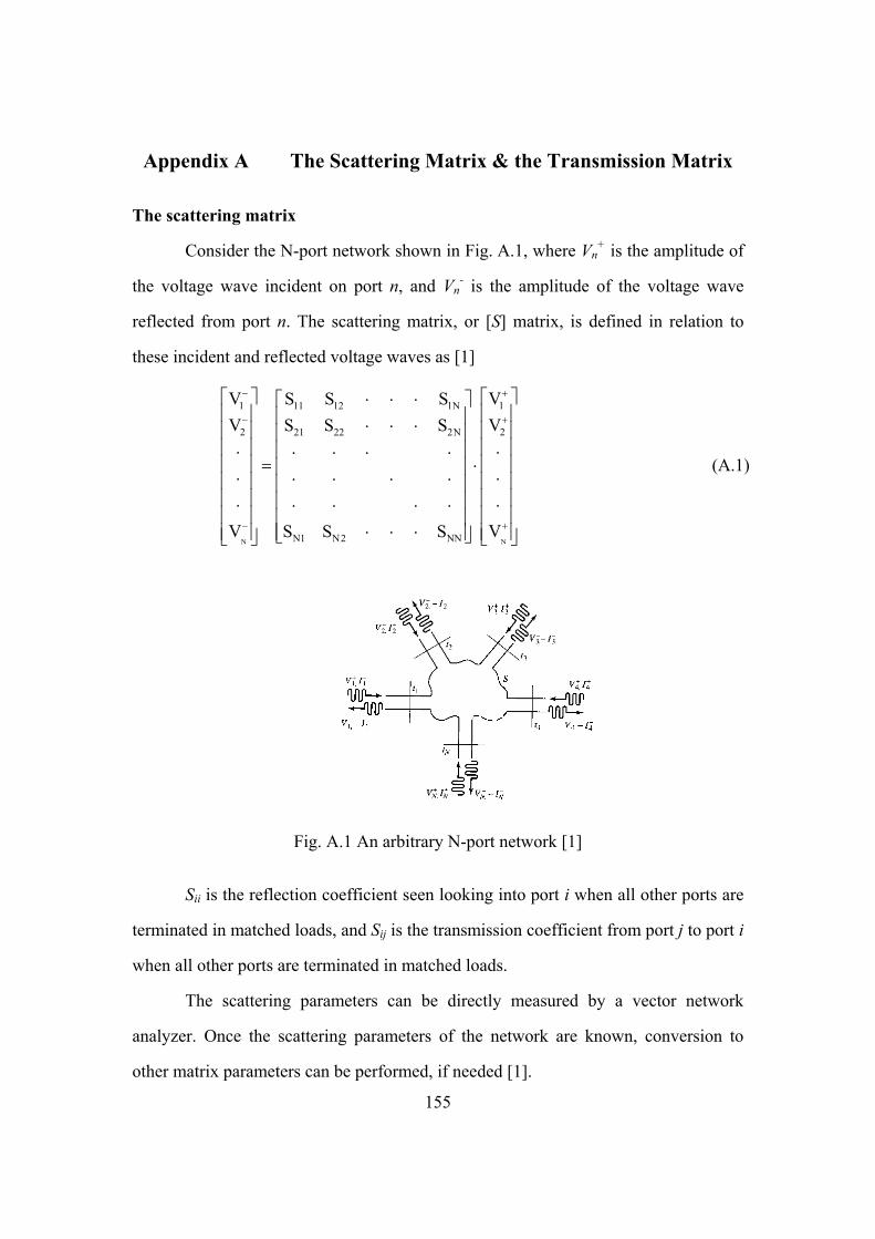
155
Appendix A The Scattering Matrix & the Transmission Matrix
The scattering matrix
Consider the N-port network shown in Fig. A.1, where Vn+ is the amplitude of
the voltage wave incident on port n, and Vn- is the amplitude of the voltage wave
reflected from port n. The scattering matrix, or [S] matrix, is defined in relation to
these incident and reflected voltage waves as [1]
N N
1 111 12 1N
2 221 22 2N
N1 N2 NN
V VS S SV VS S S
V VS S S
− +
− +
− +
⎡ ⎤ ⎡ ⎤⋅ ⋅ ⋅⎡ ⎤⎢ ⎥ ⎢ ⎥⎢ ⎥⋅ ⋅ ⋅⎢ ⎥ ⎢ ⎥⎢ ⎥⎢ ⎥ ⎢ ⎥⎢ ⎥⋅ ⋅⋅ ⋅ ⋅ ⋅
= ⋅⎢ ⎥ ⎢ ⎥⎢ ⎥⋅ ⋅⋅ ⋅ ⋅ ⋅⎢ ⎥ ⎢ ⎥⎢ ⎥⎢ ⎥ ⎢ ⎥⎢ ⎥⋅ ⋅⋅ ⋅ ⋅ ⋅⎢ ⎥ ⎢ ⎥⎢ ⎥
⋅ ⋅ ⋅⎢ ⎥ ⎢ ⎥ ⎢ ⎥⎣ ⎦⎣ ⎦ ⎣ ⎦
(A.1)
Fig. A.1 An arbitrary N-port network [1]
Sii is the reflection coefficient seen looking into port i when all other ports are
terminated in matched loads, and Sij is the transmission coefficient from port j to port i
when all other ports are terminated in matched loads.
The scattering parameters can be directly measured by a vector network
analyzer. Once the scattering parameters of the network are known, conversion to
other matrix parameters can be performed, if needed [1].
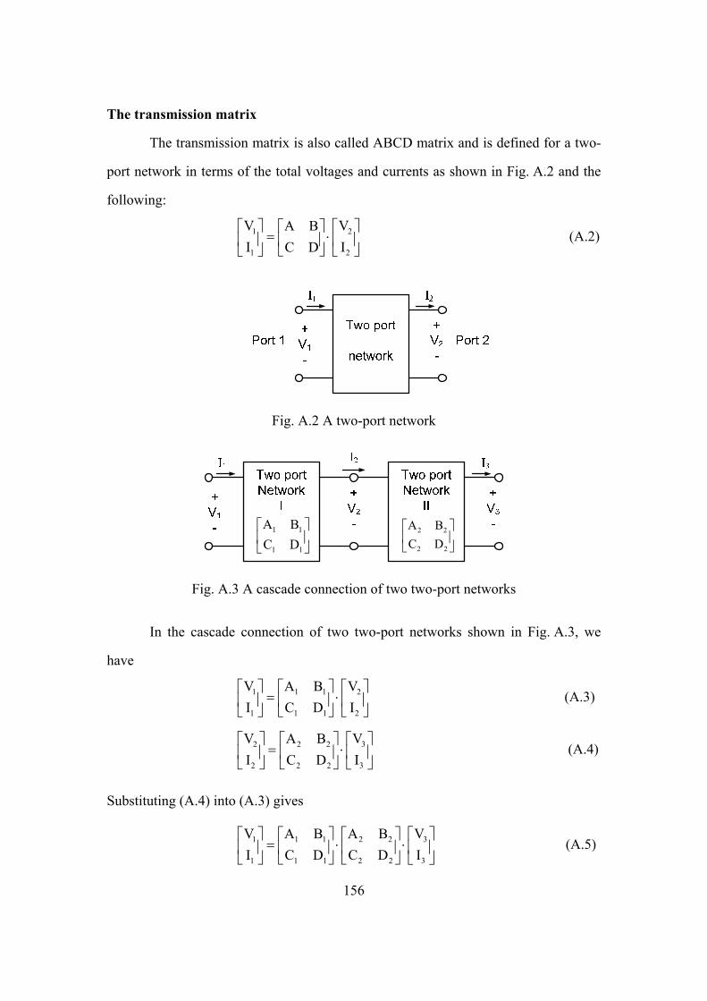
156
The transmission matrix
The transmission matrix is also called ABCD matrix and is defined for a two-
port network in terms of the total voltages and currents as shown in Fig. A.2 and the
following:
1 2
1 2
V VA BI IC D
⎡ ⎤ ⎡ ⎤⎡ ⎤= ⋅⎢ ⎥ ⎢ ⎥⎢ ⎥
⎣ ⎦⎣ ⎦ ⎣ ⎦ (A.2)
Fig. A.2 A two-port network
1 1
1 1
A BC D
⎡ ⎤⎢ ⎥⎣ ⎦
2 2
2 2
A BC D
⎡ ⎤⎢ ⎥⎣ ⎦
Fig. A.3 A cascade connection of two two-port networks
In the cascade connection of two two-port networks shown in Fig. A.3, we
have
1 1 1 2
1 1 1 2
V A B VI C D I
⎡ ⎤ ⎡ ⎤ ⎡ ⎤= ⋅⎢ ⎥ ⎢ ⎥ ⎢ ⎥
⎣ ⎦ ⎣ ⎦ ⎣ ⎦ (A.3)
32 2 2
32 2 2
VV A BII C D
⎡ ⎤⎡ ⎤ ⎡ ⎤= ⋅ ⎢ ⎥⎢ ⎥ ⎢ ⎥
⎣ ⎦ ⎣ ⎦ ⎣ ⎦ (A.4)
Substituting (A.4) into (A.3) gives
31 1 1 2 2
31 1 1 2 2
VV A B A BII C D C D
⎡ ⎤⎡ ⎤ ⎡ ⎤ ⎡ ⎤= ⋅ ⋅ ⎢ ⎥⎢ ⎥ ⎢ ⎥ ⎢ ⎥
⎣ ⎦ ⎣ ⎦ ⎣ ⎦ ⎣ ⎦ (A.5)
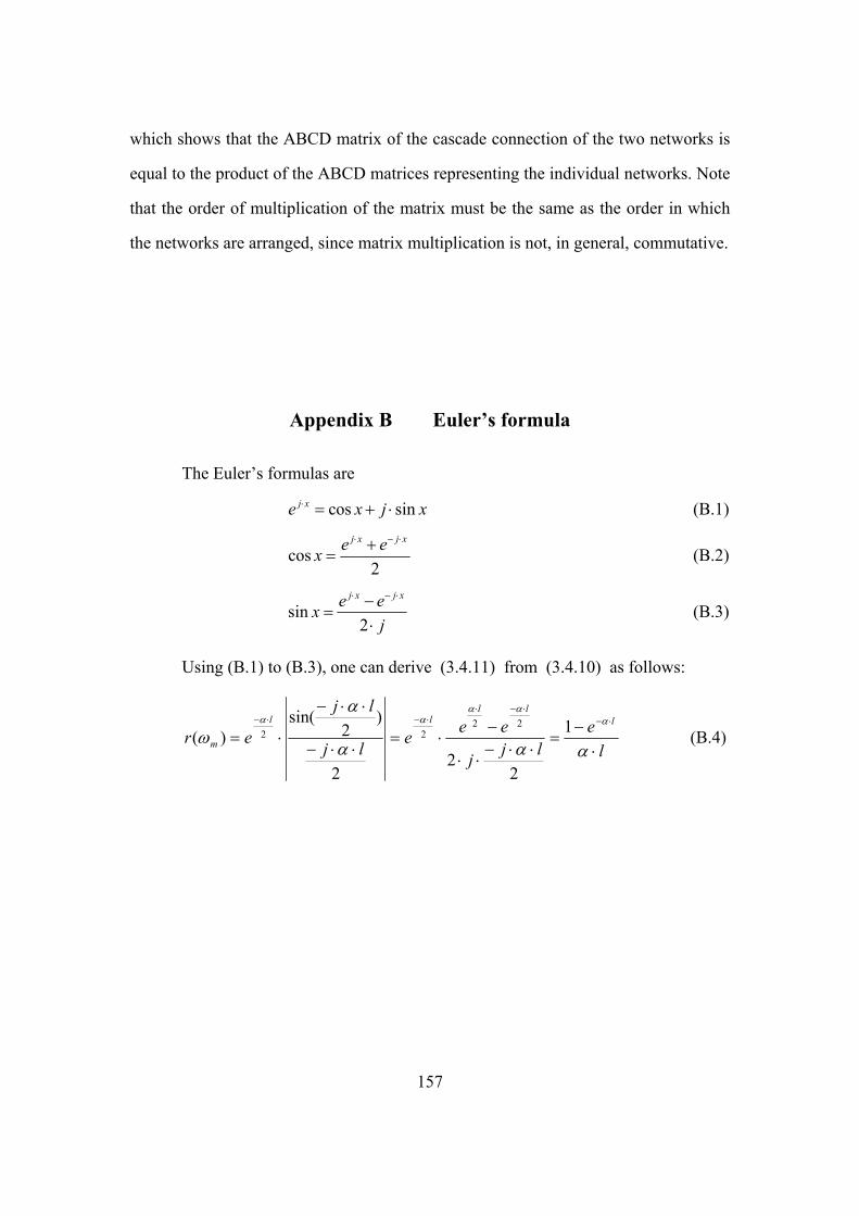
157
which shows that the ABCD matrix of the cascade connection of the two networks is
equal to the product of the ABCD matrices representing the individual networks. Note
that the order of multiplication of the matrix must be the same as the order in which
the networks are arranged, since matrix multiplication is not, in general, commutative.
Appendix B Euler’s formula
The Euler’s formulas are
cos sinj xe x j x⋅ = + ⋅ (B.1)
cos2
j x j xe ex⋅ − ⋅+
= (B.2)
sin2
j x j xe exj
⋅ − ⋅−=
⋅ (B.3)
Using (B.1) to (B.3), one can derive (3.4.11) from (3.4.10) as follows:
le
ljj
eeelj
lj
erl
llll
m ⋅−
=⋅⋅−
⋅⋅
−⋅=
⋅⋅−
⋅⋅−
⋅=⋅−
⋅−⋅⋅−⋅−
ααα
α
ωα
αααα 1
22
2
)2
sin()(
2222 (B.4)
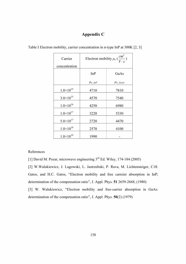
158
Appendix C
Table I Electron mobility, carrier concentration in n-type InP at 300K [2, 3]
Carrier
concentration
Electron mobility μe (2cm
V s⋅)
InP
μe_InP
GaAs
μe_GaAs
1.0×10¹⁵ 4710 7810
3.0×10¹⁵ 4570 7540
1.0×10¹⁶ 4250 6980
1.0×10¹⁷ 3220 5330
5.0×10¹⁷ 2720 4470
1.0×10¹⁸ 2570 4100
1.0×10¹⁹ 1990 -
References
[1] David M. Pozar, microwave engineering 3rd Ed. Wiley, 174-184 (2005)
[2] W.Walukiewicz, J. Lagowski, L. Jastrzebski, P. Rava, M. Lichtensteiger, C:H:
Gatos, and H.C. Gatos, “Electron mobility and free carreier absorption in InP;
determination of the compensation ratio”, J. Appl. Phys. 51 2659-2668, (1980)
[3] W. Walukiewicz, “Electron mobility and free-carrier absorption in GaAs:
determination of the compensation ratio”, J. Appl. Phys. 50(2) (1979)