Embed Size (px)
Citation preview
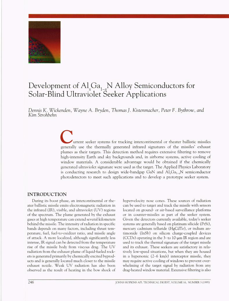
Development of Alx Ga1_xN Alloy Semiconductors for Solar-Blind Ultraviolet Seeker Applications
Dennis K. Wickenden, Wayne A. Bryden, Thomas J. Kistenmacher, Peter F. By throw, and Kim S trohbehn
C urrent seeker systems for tracking intercontinental or theater ballistic missiles generally use the thermally generated infrared signatures of the missiles' exhaust plumes as their targets. This detection method requires extensive filtering to remove high-intensity Earth and sky backgrounds and, in airborne systems, active cooling of window materials. A considerable advantage would be obtained if the chemically generated ultraviolet signature were used as the target. The Applied Physics Laboratory is conducting research to design wide-bandgap GaN and AtGa1_xN semiconductor photodetectors to meet such applications and to develop a prototype seeker system.
INTRODUCTION During its boost phase, an intercontinental or the
ater ballistic missile emits electromagnetic radiation in the infrared (IR), visible, and ultraviolet (UV) regions of the spectrum. The plume generated by the exhaust gases at high temperature can extend several kilometers behind the missile. The intensity of radiation in specific bands depends on many factors, including thrust temperature, fuel, fuel-to-oxidizer ratio, and missile angle of attack. A more localized, although significantly less intense, IR signal can be detected from the temperature rise of the missile body from viscous drag. The UV radiation from the exhaust plume of liquid-fueled rockets is generated primarily by chemically excited byproducts and is generally located much closer to the missile exhaust nozzle. Weak UV radiation has also been observed as the result of heating in the bow shock of
hypervelocity nose cones. These sources of radiation can be used to target and track the missile with sensors located on ground- or air-based surveillance platforms or in counter-missiles as part of the seeker system. Given the detectors currently available, today's seeker systems are generally based on platinum silicide (PtSi), mercury cadmium telluride (HgCdTe), or indium antimonide (InSb) on silicon charge-coupled devices (CCDs) operating in the 3- to lO-jLm IR region and are used to track the thermal signature of the target missile and its exhaust. These seekers are satisfactory in relatively low-speed situations, but when they are housed in a hypersonic (2-6 km/s) interceptor missile, they may require active cooling of windows to prevent overwhelming of the target signal by radiation from any drag-heated window material. Extensive filtering is also
246 JOHNS HOPKINS APL TEC HNICAL DIGEST, VOLUME 16, NUMBER 3 (1995)

required to prevent the high-intensity solar radiation of the Earth or sky background from reaching the active detector. Weight and system complexity problems could be obviated by shifting the sensor to the near UV and using the chemical signature of the missile exhaust as the target. One possible problem in moving to the ultraviolet is the attenuation of such radiation by atmospheric ozone. For example, Fig. 1 shows the Earth's albedo in the wavelength range of interest. 1 The ozone absorption causes a decrease in the observed radiance at a rate of 2 decades per 12 nm in the neighborhood of 305 nm. System requirements such as sensitivity and operating wavelength will thus depend on target ranges, signal-to-background ratios, altitudes, and so on. Finally, moving the detection wavelength to below 300 nm would make the system intrinsically solar blind, effectively eliminating the background signals and removing the need for the extensive filtering of the background solar radiation. It is worth noting that one version of the shoulder-launched ground-to-air Stinger missile system uses a dual-mode IR and UV tracker, although details of system performance are unknown at this time.
Current UV sensors are either intensified photocathodes with silicon CCD detectors or the even older tube intensifier and photomultiplier tube (PMT) devices. The latter are generally more efficient in the UV and have performance advantages that often compensate for the disadvantages of their bulk, fragility, and high operating voltage requirement. However, these disadvantages preclude their use in missile-borne seeker systems. Silicon CCDs, or other narrow bandgap semiconductors such as gallium arsenide (GaAs) or indium phosphide (InP) CCDs, and photodiodes suffer from a short penetration depth in the UV. As a result, the photons often fail to reach the charge-generation and storage elements of a CCD or the collection electrodes
100~------~------~--------~-------.
§ 10-1
~
.~ -e 10-2 ~ Q) u c (1j 10- 3 '6 ~ 0 "0 Q) 10-4 .0
<l:
10-5~------~------~--------~------~ 250 275 300 325 350
Wavelength (nm)
Figure 1. The albedo of the Earth in the wavelength range 250-350 nm, as measured by the Nimbus-4 Backscatter Ultraviolet Instrument.
of a photodiode. Furthermore, these materials are not intrinsically solar blind and require extensive and elaborate optical filtering to make them so, which adds complexity and decreases optical throughput.
These deficiencies could be overcome by developing semiconductor sensors based on materials with suitably wide bandgaps. Candidate material systems include silicon carbide (SiC), the Group II-VI semiconductors zinc sulfide (ZnS) and zinc selenide (ZnSe), and the Group IlIA nitrides. The hexagonal polytypes of SiC, although considered excellent candidates for blue lightemitting diodes (LEDs) and for high-temperature and high-power electronic devices, are not suitable for solar-blind UV detector applications because of their indirect and comparatively low bandgaps (bandgap energy Eg ~ 3.2 eV). Recent progress in developing blue-green LEDs and lasers in the ZnSxSel_x alloy system2 has been restricted to high-selenium alloys with bandgaps < 2.8 e V. Higher-bandgap alloys continue to be plagued by autocompensation effects that preclude well regulated conductivity control. Thus, the Group IliA nitrides are the preferred candidates for wavelength-selectable optical detectors operating in the solar-blind regions of the UV spectrum. Gallium nitride (GaN) and aluminum nitride (AIN) have direct bandgaps of 3.4 and 6.2 e V, respectively, with corresponding cutoff wavelengths of 365 and 200 nm. Since they are miscible with each other and form a complete series of aluminum gallium nitride (AlxGa1_xN) alloys, it should, in principle, be possible to develop UV detectors with wavelength cutoffs anywhere in this range.
This article describes the work being undertaken within the APL's Independent Research and Development Photonics/Electro-optics thrust area to develop GaN and AlxGa1_xN semiconductors suitable for such solar-blind UV detectors and to produce a prototype seeker system based on a conceptually simple "quad cell array" of four independent photoconductive detectors fabricated on the four quadrants of a single chip.
DEVELOPMENT OF GaN AND AlxGal_xN SEMICONDUCTORS
Background
The Group IlIA nitrides, particularly GaN, have been under investigation for several years owing to their enormous potential as detectors and uses in other opto-electronic applications. The major technological barrier to be overcome is the lack of bulk materials for use as substrates to sustain homoepitaxial growth. The inability to prepare bulk single crystals from the melt is a consequence of the extremely high vapor pressure of nitrogen in equilibrium with the compounds at elevated temperatures. For example, the vapor pressure of nitrogen over GaN is in excess of 1000 atm at
JOHNS HOPKINS APL TECHNICAL DIGEST, VOLUME 16, NUMBER 3 (1995) 247

D. K. WICKE DE ET AL.
1200°C, a temperature well below GaN's predicted melting point.3 The lack of bulk crystals results in problems associated with heteroepitaxial growth on a substrate of different chemical and physical characteristics. The room-temperature a lattice parameters of A1N and GaN are 0.311 and 0.319 nm, respectively. Possible hexagonal substrates that have a reasonable lattice match to the nitrides are a-SiC and zinc oxide (ZnO), with a lattice parameters of 0.308 and 0.325 nm, respectively. The former is produced commercially in single crystal boules up to 40 mm in diameter,4 but costs are prohibitive. The latter is chemically unstable at high temperatures in the presence of ammonia, which is used in the growth of the nitrides. The most commonly used substrate is (00.1) oriented sapphire
(a) (e)
(b) (f)
(c) (g)
(d) (h)
(a-Alz0 3), which has an a hexagonal cell constant of 0.4 7 58 nm. When deposited epitaxially on such substrates, the (00.1) plane of the GaN layer lines up parallel to that of the sapphire, but the nitride's lattice rotates 30° about the [00.1] axis such that (l0.10)GaN is parallel to (l1.0)sapphire.5 This rotation reduces the lattice mismatch between GaN and sapphire to only 16%, which is still considered inadequate for goodquality heteroepitaxial growth. As a result, growth proceeds by the three-dimensional mechanism illustrated in Figs. 2a- c. Growth commences by the nucleation of GaN at dispersed random sites on the sapphire surface (Fig. 2a). Growth then proceeds selectively on these initial nuclei, and individual islands develop (Fig. 2b), with each one being epitaxial to the substrate.
Finally, a single layer is formed by the coalescence of the islands (Fig. 2c). Facets, arising from the anisotropic growth rate of GaN, result in a surface with pronounced hexagonal features, 6 as illustrated in Fig. 2d. Similarly, the large difference in thermal expansion coefficients causes a buildup of stress during cooling that is often relieved by cracking in the sapphire and epitaxial layers near the interface,? as is also evident in Fig. 2d.
It has been shown that thin buffer layers of either A1N8,9 or GaNlO,ll
Figure 2. Effect of nucleation layer on growth morphology of GaN on (00.1) sapphire. (a) Random nucleation of GaN on bare a-AI20 3; (b) selective growth of these nuclei; (c) eventual coalescence to form a continuous layer. (d) The resultant GaN layer has a faceted surface. (e) The use of a lowtemperature buffer layer leads to a (f) much higher density of nucleation sites and (g) subsequent pseudo-two-dimensionallayer growth. (h) The resultant GaN layer has a virtually featureless surface.
predeposited at low temperatures, particularly on (00.1) oriented sapphire, greatly improve the crystallographic, electrical, and optical properties of GaN . We have previously determined1z by extensive optical and X-ray measurements that GaN nucleation layers deposited at 540°C have a measurable crystalline component, although the X-ray data and the lack of absorbance features near the direct bandgap of GaN suggest that the crystallites are very small
248 JOHNS HOPKINS APL TECHNIC AL DIGEST, VOLUME 16, NUMBER 3 (1995)

and are most probably embedded in an amorphous-like matrix. Upon annealing to higher temperatures, the crystallite size increases and the crystal perfection improves markedly, until at temperatures near those empirically determined to be optimum for growth of an epitaxial overlayer, the perfection approaches that of good quality single-crystal material. These buffer layers serve to provide a high density of nucleation sites for the growth of the overlayers, as illustrated schematically in Figs. 2e and 2f. Such a high density of nucleation sites means that the overlayer needs to grow only a few nanometers before it coalesces and forms a continuous layer. This layer proceeds to grow by a pseudo-twodimensionallayer-by-layer mechanism, as illustrated in Fig. 2g. A photograph of such a self-nucleated overlayer is shown in Fig. 2h (with the same magnification as Fig. 2d), and it is distinguished by the lack of surface structure.
The improvements in the growth and characteristics of GaN have resulted in significant inroads in device technology. 13 For example, high-efficiency blueemitting metal-insulator-semiconductor LEDs14 have been fabricated, and with the advent of Mg-doped p-type material, violet emitting pn-junction LEDs15,16 have been developed. Prototype GaN metal semiconductor field-effect transistors have also been reported. 17 In addition, high-quality, low-aluminum-content GaN/ AtGal_xN heterostructures have been produced that exhibit quantum confinement effects by photoluminescence,18 stimulated emission under photon pumping,19,20 and electron mobility enhancement.21 Finally, violet-emitting indium gallium nitride (Inl_xGaxN)/ GaN LEDs with external quantum efficiencies of 0.22 % have been developed, 22,23 and double-heterostructure blue- and green-emitting Inl_xGaxN/AlyGal_yN LEDs with external quantum efficiencies as high as 2.7% have recently been reported.24,25
These results demonstrate that GaN and its alloys can no longer be regarded as "semiconductors of the future," particularly since some Inl_xGaxN/AlyGal_yN devices are currently moving to full-scale production. However, it should be noted that the ternary alloy systems have been characterized much less than GaN. Although solid solutions in the Al- Ga- N system were first reported in 197326 and epitaxial layers of AlxGal_xN on sapphire were reported in 1978,27 few comprehensive studies have been undertaken on the growth and characterization of these materials, and some controversy on their physical, optical, and electrical properties remains.
Experimental R esults
Growth
We have studied the growth of self-nucleated AtGal_xN films on (00.1) oriented sapphire substrates using a vertical spinning disc metallo-organic chemical
ALLOY SEMICONDUCTORS FOR SEEKER APPLICATIONS
vapor deposition (MOCVD) reactor operating at 70 torr. 28 Trimethylgallium (TMG), trimethylaluminum (TMA), and ammonia (NH3) in a nitrogen (N2) carrier gas were used as starting reagents. Before being loaded, the substrates were given an ultrasonic rinse in mild detergent and washed in 5: 1: 1 mixtures of hot H20:HN03:H20 2 and H 20:HC[:H20 Z' rinsed in deionized H20, and dried with filtered N 2 gas. In addition, the substrates were heated in situ at 850°C for 5 min. The self-nucleation layers were deposited for periods ranging from 120 to 360 s at 540°C (as measured with an optical pyrometer) using a combined TMA and TMG gas flow in the range of 67 to 87 j.tmole/min, an NH3 gas flow of 22 X 10-3 mole/min, and an N 2 gas flow of 4.0 standard L/min. The deposition rate of the nucleation layer varied with the TMA/TMG ratio in the gas phase such that the layer's thickness was estimated to be in the range of 20 to 50 nm. The overlayers were grown at 1025°C using the same TMA and TMG flows. The growth rate of the overlayer was approximately independent of alloy composition at 1.2 j.tm/h, and total thickness was in the range of 0.8 to 1.8 j.tm.
All films were smooth and specular, and any growth features followed only from nonoptimized buffer layers. 29 There was also no indication that any other properties were influenced significantly by the variation in buffer layer thickness or other deposition parameters.
Composition and Structure
Alloy compositions x as determined by X-ray energy dispersive spectroscopy and by X-ray diffraction measurement of the lattice constants agreed to within ±0.02, confirming that Vegard's law is obeyed for these self-nucleated AtGal_xN films. This finding is in accord with Koide et al.,30 who prepared AtGal_xN alloys on both (00.1) sapphire and (111) silicon substrates using atmospheric pressure MOCVD, and it contradicts the results of Yoshida, Misawa, and Gonda,3l who studied films prepared by reactive molecular beam epitaxy and concluded that the lattice constant was not a linear function of alloy composition. The high-crystalline quality of our AtGa l-xN alloy films is evidenced by the ()/2() X-ray diffractometer scans shown in Fig. 3 for a selection of alloy compositions in the range 0 ~ x ~ OA. As for GaN itself, the (00.1) plane of the AtGal_xN layer parallels that of the sapphire substrate, and the clear separation in the Kal/Ka2 doublets for the lowangle (00.2) reflection shows that the structural coherence parallel to the growth direction is excellent. The full-width at half maximum (FWHM) from a Lorentzian fit to the Kal component is depicted as a function of alloy composition in Fig. 4. It should be noted that from the characteristics (CuKal; 2() =
41.71°; FWHM = 2.9 arc-min) of the (00.6) reflection from the sapphire substrate, the minimum FWHM for
JOHNS HOPKINS APL TECHNICAL DIGEST, VOLUME 16, NUMBER 3 (1995) 249

D. K. WICKENDEN ET AL.
1.0
0.8 x= 0.06
Ul x = 0.18 C :J 0 0.6 u "0 Q)
.~ cti 0.4 E 0 z
0.2
0 34.0 34.5 35.0 35.5 36.0
Diffraction angle (deg)
Figure 3. Normalized X-ray diffraction intensity profiles (0120 scan) of self-nucleated AlxGa1-x N layers with x < 0.4.
the CuKa1 line from the (00.2) GaN reflection is estimated at 3.0 arc-min. It can be seen that the FWHM increases mildly with increasing alloy composition, implying minimal increases in physical and chemical inhomogeneity on alloying. Using the X-ray precession method,32 the quality of the in-plane heteroepitaxy
has also been assessed as a function of alloy composition. In line with the trend in the c-axis length with x, the a-axis length varies linearly with composition, with a gradient correlating with the different c/a ratios of GaN and AIN. Furthermore, the in-plane azimuthal coherence (mosaic spread) deteriorates slightly across the series, presumably in parallel with the weakly degraded structural coherence seen in the film growth direction.
To assess the misorientation of the mosaic of AtGal_xN islands relative to the growth direction (polar dispersion) more fully, X-ray rocking curves through the (00.2) reciprocal lattice vector were recorded. These rocking curves are shown in Fig. 5, and three features of the scattering profiles are immediately discernible: (1) there is a shift to higher () with increasing x that reflects the decreasing c lattice constant; (2) the peak widths are of the order of tenths of a degree and are much larger than that [0.005°] for the comparable (00.6) reflection from the sapphire substrate; and (3) there is a systematic broadening of the FWHM for the X-ray rocking with increasing x (shown in Fig. 4), signaling a decrease in orientational coherence. A point to be emphasized is that this increase in out-ofplane mosaic spread with increasing x is unlikely to result from a significant increase in inhomogeneous strain, as the calculated lattice mismatch actually improves (ultimately by about a percent) with increasing Al content.
The in-plane mosaic morphology of the films was further confirmed by scanning tunneling microscopy
10 100
8 80 C ~ .~
6 60 Ei= 2 2 ~ ~ ~ 4 40 ~ I I ~ ~ LL
2 20 LL
0 0 0 0.1 0.2 0.3 0.4 0.5
Alloy composition (x)
Figure 4. Full width at half maximum (FWHM) of X-ray diffractometer 0120 scans and X-ray rocking curve 0 scans as functions of alloy composition x. The solid lines are guides to the eye.
1.2
1.0
Ul 0.8 C :J 0 U
"0 0.6 Q)
. ~ cti E 0.4 0 z
0.2
17.0 17.5 18.0 18.5
() (deg)
Figure 5. Normalized X-ray rocking curves (0 scan) through the (00.2) reflection for self-nucleated AlxGa1-xN layers with alloy composition x < 0.4.
(STM), which showed that all films consisted of a dense mosaic of highly oriented grains, with disk-like features yielding surface height modulations of 1-2 nm and average island diameters on the order of a few tenths of a micrometer. It was further apparent that island size significantly decreased with increasing x. In fact, as in the case of the FWHM of the X-ray rocking curve, the decrease in island size was also linearly correlated with film composition.
A similar reduction in grain size with increasing x has been noted by Koide et al.33 for AlxGa1_xN thin films grown on AIN-buffered (00.1) sapphire. There the grain size decreased markedly from about 400 nm for a GaN film to 60 nm for a film with x = 0.1 as estimated from a combination of () and ()/2() X-ray scans. In contrast, we found that, for a more extended series of self-nucleated films, the feature size, as determined by the real-space STM scans and inferred from X-ray () scans, diminishes much less rapidly. The common decrease in grain size in each set of films implies a
250 JOHNS HOPKINS APL TECHNICAL DIGEST, VOLUME 16, NUMBER 3 (1995)

parallel reduction in a growth factor influenced by increasing Al content. Across the set of AIN -nucleated films ofKoide et al., there is a common nucleation layer whose lattice mismatch with the overlayer decreases with increasing Al content. It might be anticipated in that case that the grain size could in fact increase with increasing x (in contrast to our experiment). In the films we studied, the nucleation layer composition nominally matches that of the overlayer and could lead to the naive speculation that the grain size might remain constant (again in contrast to experiment). These conflicting results suggest, in fact, that lattice-matching the nucleation layer and overlayer is not a predominant factor in modifying the growth mode, although the reduction in grain size with increasing x is considerably less pronounced for the self-nucleated films. The comparison of results demonstrates that a reduction in surface mobility or nucleation site density with increasing Al content dominates the growth process for the AlxGal_xN overlayers.
Optical Properties
We assessed the optical quality of the films from the optical absorption in the bandgap region. Figure 6 shows a plot of the square of the absorption coefficient a as a function of photon energy hll. The solid lines are drawn from the point of maximum gradient in the absorption curves, and their extrapolated intercepts are used to calculate the optical direct bandgap energies Eg of these AlxGa l-xN alloys. The absorption curves do not exhibit the large low-energy tails observed in other studies,27,34 indicating again that macroscopic nonuniformities in the samples are minimal. In fact, probing the films with a 1-mm-diameter beam aperture showed a variation of less than ±0.02 e V in the derived Eg,
corresponding to a variation in x of less than 0.01. The high optical quality of these alloys has also been confirmed by studies of their nonlinear optical characteristics.
A plot of the optical bandgap energy Eg as a function of the alloy composition x is given in Fig. 7 and shows a nominally linear dependence of Eg on x with a bowing parameter b"", 0 e V. Here, the bowing parameter is defined by the experimentally determined equation of the variation in Eg of a ternary alloy AxB1-xC on the alloy x:
Eg(x) = XEg,AC + (l-X)Eg,BC - bx(l-x) .
This is in agreement with the results of Khan et al. ,35 although it would seem from the presented data that the bandgap of those authors' material was consistently higher than expected. It does not agree with the results of Yoshida, Misawa, and Gonda,31 who concluded that there was a small negative bowing parameter, which they estimated to be -0.8 e V. Neither does it agree with the results from the Nagoya group, who studied both unnucleated34 and nucleated36 samples and determined
ALLOY SEMICONDUCTORS FOR SEEKER APPLlCA TIONS
a positive bowing parameter of 0.98 eV. The magnitude of these discrepancies is illustrated in Fig. 7 by the lines representing the reported range of b values.
It is difficult to resolve these differences fully, although it is noted that both the lattice constant and energy gap of a particular AlxGal_xN film are functions of any residual strain present. Moreover, since absorption coefficients are greater than 104 cm- 1 near the band edge, the optical gaps are in practice determined using samples thinner than "",3 f.Lm. It is further noted that GaN films grown on AIN -nucleated sapphire substrates either by MOCVD or by hydride vapor phase epitaxy have significant residual strain owing to a combination of lattice and thermal expansion coefficient mismatch.37 This residual strain gradually decreases in those films at thicknesses greater than 4 f.Lm,
and the films become completely relaxed by "",100 f.Lm.
In contrast, we have previously shown that GaN nucleation layers deposited on (00.1) sapphire substrates become fully relaxed by the time that they have been
40
x= 0 .00
0.06 30
N 0.18
0.20 I E u
co 0 20
2S C\J ~
10
0 3.2 4.6
Photon energy (eV)
Figure 6. Absorption coefficient squared (ci) as a function of photon energy hv for AlxGa1-xN alloys with x < 0.4.
5.00,-----,------r-------,---,----::;;>'1
> ~
uY' 4.50 >. 0')
Q) c Q)
Q. 4 .00 co 0') '0 C co .0 ~ 3.50 u li o
3.00 L-__ ----'---_ __ -'--__ ---'--___ -'---_ _ ---"
o 0.1 0.2 0.3 0.4 0.5
Alloy composition (x)
Figure 7. Optical bandgap energy of AlxGa1-xN layers as a function of alloy composition x. The black line represents bowing parameter b = 0; the other lines represent the range of b values reported in the literature.
JOHNS HOPKINS APL TECHNICAL DIGEST , VOLUME 16, NUMBER 3 (1 995) 251

D. K. WICKENDE ET AL.
ramped from their deposition temperature to the growth temperature of the GaN overlayer,38 a result that is independent of film thickness. We speculate at this time then that the widely different results for the trends in optical bandgaps in AlxGa1_xN alloys are attributed to an equal variance in the residual strain in various samples. Further work is in progress to fully clarify this point.
Electrical Properties
As is the case with APL-grown GaN, the AlxGa1_xN layers are electrically insulating when no intentional dopant is present in the gas stream. To fabricate useful semiconductor junction devices, it is necessary to be able to produce both n- and p-type material with controlled transport characteristics. Initial studies have been undertaken on the growth and characterization of silicon-doped n-type AtGa1_xN alloys obtained by adding silane to the growth stream during the deposition of the overlayer, as had been previously demonstrated with GaN.39
Figure 8 shows the carrier concentration as a function of alloy composition x for selected ratios of silane (SiH4) to Group III metallo-organic compound in the vapor phase. It can be seen that, for each ratio studied, there is a monotonic decrease in observed carrier concentration with increasing x. Studies are in progress to determine whether this decrease is correlated with either a change in silicon incorporation efficiency with increasing x or with a change in dopant activation. The mobility as a function of carrier concentration for the range of AlxGa1_xN alloy compositions studied here is shown in Fig. 9. Mobility decreases dramatically with increasing values of x. Similar drops in either or both carrier concentration and mobility with increasing x in undoped AtGa 1-xN alloys have been observed by other workers,30,3 1,35 ,40 who have generally found that sam-ples with x ~ 0.4 become insulating.
Photoluminescence studies on undoped samples have provided no evidence that the sharp change in resistivity arises from an increase in depth of a native donor defect with increasing aluminum composition of the alloy.4l This finding is in accord with theoretical predictions of the location of energy levels associated with native defects in the Group IlIA nitrides,42 leaving either compensation by an increasing number of deep acceptors (which 'could be responsible for the observed drop in carrier concentration with increasing x) or the appearance of another carrier scattering mechanism (which could be responsible for the drop in mobility with increasing x) as the major cause of the results. Possible scattering mechanisms include straightforward alloy scattering resulting from local compositional fluctuations on the atomic scale or some form of "grain boundary" scattering caused by the decrease in feature size with increasing Al content of the alloy.
7' E ~ c o
~ C Q) u c
1019
8 1018 m ·c ~ ()
o 0.10 0.20 0.30 0.40
Alloy composition (x)
Figure 8. Carrier concentration of AlxGa1-xN layers as a function of alloy composition for various ratios of SiH4 to Group III metalloorganic compound in the vapor phase.
200
5- 150 E ~
~ 100 :0 o ~
50
Carrier concentration (cm- 3)
Figure 9. Mobility of AlxGa1 _x N layers as a function of carrier concentration for various alloy compositions.
More detailed studies are necessary to fully understand these results and their implications for devices containing high x value AlxGa 1-xN alloys.
DEVELOPMENT OF PROTOTYPE UV SEEKER SYSTEM
GaN and AlxGal_xN Photodetectors
The results outlined previously demonstrate an MOCVD growth technology capable of yielding semiinsulating GaN and AlxGa1_xN alloys of high optical and structural quality. This technology is based on the use of self-nucleation layers and a firm understanding of how these layers influence subsequent growth of the epitaxial layer to yield semi-insulating GaN under standard continuous growth conditions. This material is suitable for processing into photoconductive detectors, and prototype GaN devices have been fabricated in
252 JOHNS HOPKINS APL TECHNICAL DIGEST, VOLUME 16, NUMBER 3 (1995)

collaboration with the Naval Research Laboratory. The devices are composed of a set of interdigitated electrodes with finger separations of approximately 35 and 3 /lm. The response of the 35 -/lm devices was more than an order of magnitude lower than the 3-/lm devices, most probably because of the high surface recombination velocity of photogenerated carriers observed in direct gap semiconductors. The performance of a representative sample of the 3-/lm devices under an illuminated power density of approximately 40 m W/cm2 at 300 nm is shown in Fig. 10. It can be seen that the device exhibits an extremely low dark current, that the photocurrent saturates quickly, and that the current recovers relatively rapidly after the illumination is switched off, indicating that few deep traps are present in the material. Gains as high as 600 are observed. This performance is comparable to that of GaN photoconductive devices reported by other workers.43 The dark current is not affected by illumination with belowbandgap light of 400 nm. There are no previous reports in the literature of photodetector devices being developed from AlxGal_xN alloys. Moreover, it is expected that the quality of the material described earlier will be suitable for the development of a laboratory prototype seeker system. Photoconductive devices will be made from various alloy compositions, including x ~ 0.28, which inspection of Fig. 7 shows will have cutoff wavelengths of 300 nm (4.13 e V) and below. These devices will be developed in collaboration with researchers at NASA, Goddard.
Prototype System
T o serve as a detector head in seeker systems, the photodetector device needs to be operated as a positionsensitive detector. The simplest practical way to achieve this is in a quadrant geometry in which four independent photodetectors are fabricated on a single chip with the minimum of dead space between them, a so-called quad cell array. The optical system is designed such that the size of the image, when centered on the quad cell array, overlaps all four elements, thus giving equal output signals to the control electronics, as detailed in Fig. 11. As the image deviates from center, these output signals change, and the relative changes are used to compute the movement of the target. It is a comparatively simple task to program any servo-controlled guidance system to maintain the image at the center of the array.
A block diagram of the prototype system is shown in Fig. 12. A simple F/6 telescope focuses a UV spot, generated in the first instance from a small pen-ray lamp, onto the GaN or AlxGal_xN quad cell. A preamplifier conditions the quad cell output, and a 68HC11 single-chip microcontroller digitizes the four preamplifier outputs and computes position error signals in software. This approach allows the system to be easily changed
ALLOY SEMICONDUCTORS FOR SEEKER APPLICATIONS
10--4
10-5
10--6
~ 10- 7 C ~ 10-8 ~ U
10-9
10- 10
I'-...... 10- 11
o
Light on
50 I
Light off
t
100
Time (s)
I
150 200
Figure 10. Characteristics under illumination of prototype GaN photoconductive detector. The illumination (40 mW/cm2) at 300 nm is turned on at :::50 s and turned off at :::112 s.
Common
x=
Y=
(fB+/d-(IA+iO)
IA + IB + Ie + 10
(Ie + 10 ) - (fA + IB)
IA+/B+Ie+io
Y
Lx
Figure 11. Schematic diagram of prototype AlxGa1-xN photoconductive quad cell. The position coordinates are x and y and the currents from the separate quadrants are IA . lB . Ie . and 10.
to accommodate the various characteristics to be expected from different batches of devices. The design is also capable of balancing out nonuniformities in individual quad cell arrays. The telescope position is controlled by radio control servo positioners that produce a shaft position proportional to a pulse width between 1 and 3 ms. The pulse-width-modulated elevation and azimuth signals are generated by the microcontroller to position the telescope in such a manner as to nullify the quad cell position error signals. The electronics are battery powered, since the prototype system is intended to be portable.
Photographs of the front and side views of the prototype seeker assembly, mounted on a base plate about
JOHNS HOPKINS APL TECHNICAL DIGEST, VOLUME 16, NUMBER 3 (1 995) 253

D. K. WIC KE DE ET AL.
the size of a standard sheet of paper, are shown in Fig. 13. A small box (not shown) contains the electronics and batteries. The telescope is mounted on an azimuth pedestal so that the range of travel is -30 to +900 in azimuth. The entire assembly can be packed in an instrument case for ease of transport.
SUMMARY Moving the target of an inter
continental or theater ballistic missile seeker system from the thermally generated infrared signature of the exhaust plume to the chemically generated ultraviolet signature could result in significant savings in system weight and complexity. Such a move would require the development of suitable UVsensitive solid-state detectors. We have demonstrated that AlxGal_xN alloy semiconductors, which have direct bandgaps in the range from 3.4 to 6.2 e V, are ideally suited for such applications. Moreover, APL has developed an M OCVD growth technology capable of producing high-quality alloys with 0 ~ x ::; 0.4. The maximum alloy composition in this range, with a bandgap of 4.4 e V, corresponding to a wavelength cutoff of 280 nm, is useful for fabricating intrinSically solar-blind detectors. Unintentionally doped material is semi-insulating, having characterlStlCS suitable for good-quality photoconductive devices. Such devices are being used to develop a prototype bench-top tracking system based on a position-sensitive detector using a simple photoconductive quad cell. N-type doping has been achieved by adding SiH4 to the gas stream. Preliminary indications are that the electrical characteristics degrade with increasing aluminum composition, although the reasons for this degradation are unknown at this time. If it proves possible to produce p-type AlxGal_xN alloys, the development of more complex photovoltaic diodes and arrays will be feasible.
254
25mm FI6
Figure 12. Block diagram of prototype UV seeker.
(a)
(b)
Figure 13. Photographs of prototype UV seeker. The electronics box is not shown. (a) Side view. (b) Front view.
JOHNS HOPKINS APl TECH ICAl DIGEST, VOLUME 16, NUMBER 3 (1995)

REFERENCES
IHeath, D. F., Krueger, A. ] ., Roeder, H. A., and Henderson, B. D., "The Solar Backscatter and Total Ozone Mapping Spectrometer (SBUV(TOMS) for
IMBUS G," Opt. Eng. 14,323-33 1 (1975). 2Gunshor, R. L. and Nurmikko, A. V., "The First Compact Blue/Green Diode
La ers-Wide-Bandgap II-VI Semiconductors Come of Age," Proc. IEEE 82, 1503-1 513 (1994).
3Thurmond, C. D., and Logan, R. A., "The Equilibrium Pressure of 2 over GaN," J. Electrochem. Soc. 119,622-626 (1 972) .
4Davis, R. F., Kelner, G., Shur, M. Palmour, ]. W., and Edmond, ]. A., 'Thin Film Deposition and Microelectronic and Optoelectronic Device Fabrication and Characterization in Monocrystalline Alpha and Beta Silicon Carb ine,"
,Proc. IEEE 79, 677-7017 (1991). JWickenden, D. K., Faulkner, K. R. , Brander, R. W., and Isherwood, B. ].,
"Growth of Epitaxial Layers of Gallium itride on ilicon Carbide and Corundum Substrates," J. Cryst. Growth 9 , 158-164 (1 97 1).
6Sasaki , T , and Zembutsu, S., "Substrate-Orientation Dependence of Ga Single-Crystal Films Grown by Metalorganic Vapor-Phase-Epitaxy," J. Appl. Phys. 61 , 2533- 2540 (1987).
7Itoh, N., Rhee, ]., Kawabata, T, and Koike, S., "Study of Cracking Mechanism in Ga /a-AI203 Structure," J. Appl. Phys. 58, 1828-1837 (1985).
8Yoshida, S., Misawa, S., and Gonda, A., "Improvements on the Electrical and Luminescent Properties of Reactive Molecular Beam Epitaxially Grown GaN Films by Using AIN-Coated Sapphire Substrates," Appl. Phys. Lett. 42,427-429 (1983).
9 Amano, H., Sawaki, ., Akasaki, I. , and Toyoda, Y., "Metalorganic Vapor Phase Epitaxial Growth of a High Quality Ga Film Using an AIN Buffer Layer," Appl. Phys. Lett. 48, 353-355 (1986).
lOWickenden, D. K., Kistenmacher, T. ] ., Bryden, W. A., Morgan, ] . S., and Wickenden, A. E., "The Effect of Self ucleation Layers on the MOCVD Growth of Gallium itride on Sapphire," Mater . Res. Soc. Symp. Proc. 221 , 167-172 (1991).
IINakamura, S., "GaN Growth Using GaN Buffer Layer," Jpn. J. Appl. Phys. 30, Ll705-1707 (1991).
12Wickenden, A. E., Wickenden, D. K., and Kistenmacher, T ]. , "The Effect of Thermal Annealing on Ga ucleation Layers Deposited on (0001) Sapphire by Metalorganic Chemical Vapor Deposition," J. Appl. Phys. 75 , 5367-5371 (1994) .
13Strite, S., and Morko~, H., "Ga ,AIN, and InN: A Review," J. Vac. Sci. Technol. B 10, 1237-1266 (1992).
14Akasaki, I., Amano, H., Hiramatsu, K., and Sawaki, ., "High Efficiency Blue LED Utilizing Ga Film with AIN Buffer Layer Grown by MOVPE," Inst. Phys. Conf. Ser. 91 , 633-636 (1988).
15 Amano, H., Kito, H. , Hiramat u, K., and Akasaki I. , "P-Type Conduction in Mg-Doped GaN Treated with Low-Energy Electron Beam Irradiation (LEEB!)," Jpn. J. Appl. Phys . 28, L2112-2114 (1989).
16Nakamura, S., Mukai, T ., and Senoh, M., "High-Power Ga p-n Junction Blue-light-Emitting-Diodes," Jpn. ]. Appl. Phys. 30, Ll 998-2001 (1991).
17Khan, M. A. , Kuznia,]. ., Bhattarai, A. R., and Olson, D. T , "Metal Semiconductor Field Effect Transi tor Based on Single Crystal Ga ," Appl. Phys. Lett. 62,1786-1787 (1993).
18Itoh, K., Kawamoto, T , Amano, H., Hiramatsu, K. , and Akasaki, I., "Metalorganic Vapor Phase Epitaxial Growth and Propert ies of GaN/ AIO.IGaO.9N Layered Structures," Jpn. J. Appl. Phys. 30, 1924-1927 (1991).
19 Amano, H., Asahi, T, Kito, M., and Akasaki, I., "Stimulated Emission in MOVPE-Grown Ga Film," J. Lumin. 48 & 49, 889-892 (1991).
20Khan, M. A., Olson, D. T., Van Hove, ]. M., and Kuznia, ]. N., "VerticalCavity, Room-Temperatu re Stimulated Emission from Photopumped Ga Films Deposited over Sapphire Substrates Using Low-Pressure Metalorganic Chemical Vapor Deposition," Appl. Phys. Lett . 58, 1515-1517 (1991).
21Khan, M. A. , Van Hove, ]. M., Kuznia, ]. N., and Olson, D. T, "High Electron Mobility GaN/AlxGal_x Heterostructures Grown by Low-Pressure Metalorganic Chemical Vapor Deposition," Appl. Phys. Lett. 58, 2408-2410 (1991).
22Nakamura, S., Senoh, M., and Mukai, T, "High-Power InGaN/GaN DoubleHeterostructure Violet Light Emitting Diodes," Appl. Phys. Lett. 62 , 2390-2392 (1993) .
23 akamura, S., Senoh, M., and Mukai, T, "p-GaN/n-InGaN/n-Ga DoubleHeterostructure Blue-light-Emitting Diodes," Jpn . J. Appl. Phys. 32, L8-11 (1993).
ALLOY SEMICONDUCTORS FOR SEEKER APPLICATIONS
24Nakamura, S., Mukai, T , and Senoh, M., "Candela-Class High-Brightness InGaN/AlGaN Double-Heterostructure Blue-Light-Emitting Diodes." Appl. Phys. Lett. 64, 1687-1689 (1994).
25Nakamura, S., Mukai, T., and Senoh, M., "High-Brightness InGaN/AlGaN Double-Heterostrucure Blue-Green-Light-Emitting Diodes," J. Appl. Phys. 76,8189-8191 (1994).
26Lyutaya, M. D., and Bartnitskaya, T S., "Thennal Stability of Complex Nitrides of Subgroup IIIB," Inorg. Mater. (Engl. Tran I.) 9 , 1052-1055 (1973) .
27Hagen, ] ., Metcalfe, R. D., Wickenden, D. K., and Clark, W., "Growth and Properties of AlxGal_xN compounds," J. Phys. C: Solid State Phys. 11 , Ll43-146 (1978).
28Wickenden, D. K., Bargeron, C. B. , Bryden, W. A., Miragliotta, ]., and Kistenmacher, T ] ., "High Quality Self-Nucleated AlxGal-x Layers on (00.1) Sapphire by Low-Pressure Metalorganic Chemical Vapor Deposition," Appl. Phys. Lett. 65 , 2024-2026 (1994).
29Wickenden, D. K., Miragliotta, ]. A., Bryden, W. A., and Kistenmacher, T ]., "Thermally Annealed GaN ucleation Layers and the Device-Quality Metalorganic Chemical Vapor Deposition Growth of Si-Doped Ga Films on (00.1) Sapphire," J. Appl. Phys. 75 , 7585-7590 (1994).
30Koide, Y., ltoh, H. , Sawaki, N., Akasaki, I., and Hashimoto, M., "Epitaxial Growth and Properties of AlxGal-x by MOVPE," ]. ElectTochem. Soc. 133, 1956-1960 (1986).
31Yoshida, S., Misawa, S., and Gonda, S., "Properties of AlxGal-xN Films Prepared by Reactive Molecular Beam Epitaxy," J. Appl. Phys. 53,6844-6848 (1 982).
32Kistenmacher, T ]. , Bryden, W. A., Wickenden, D. K., and Ecelberger, S. A., "Substrate Dependent Texture and Heteroepitaxy for Group IlIA Nitride Films by the X-ray Precession Method," Mater. Res. Soc. Symp. Proc. 208, 357- 362 (1991).
33Koide, Y., ltoh, ., Itoh, K., Sawaki, ., and Akasaki, I. , "Effect of AlN Buffer Layer on AIGaN/a-AI203 Heteroepitax ial Growth by Metalorganic Vapor Phase Epitaxy," Jpn . J. Appl. Phys. 27 , 1156-1161 (1988) .
34Koide, N., ltoh, H., Khan, M. R. H. , Hiramatsu, K., Sawaki, N., and Akasaki, I., "Energy Band-Gap Bowing Parameter in an AlxGal_xN alloy," J. Appl.
3, Phys. 6 1,4540-4543 (1987). JKhan, M. A., Skogman, R. A., Schulze, R. G., and Gershenzon, M.,
"Properties and Ion Implantat ion of AlxGal-x Epitaxial Single Crystal Films Prepared by Low Pressure Metalorganic Chemical Vapor Deposition," Appl. Phys. Lett. 43 , 492-494 (1983).
36Itoh, K. , Amano, H., Hiramatsu, K., and Akasaki, I., "Cathodoluminescence Properties of Undoped and Zn-Doped AlxGal_xN Grown by Metalorganic Vapor Phase Epitaxy," Jpn . J. Appl. Phys. 30, 1604-1608 (1991) .
37Hiramatsu, K., Detchprohm, T, and Akasaki, I. , "Relaxation Mechanism of Thermal Stre es in the Heterostructure of Ga Grown on Sapphire by Vapor Phase Epitaxy," Jpn . J. Appl. Phys. 32, 1528-1533 (1993).
38Wickenden, A. E., Wickenden, D. K., and Kistenmacher, T ]., "The Effect of Thermal Annealing on GaN ucleation Layers Deposited on (0001) Sapphire by Metalorganic Chemical Vapor Deposition," J. Appl. Phys. 75 , 5367- 5371 (1994).
39Wickenden, D. K., and Bryden, W. A., "The Growth and Characterization of Silicon-Doped GaN," Inst. Phys. Conf. SeT. 137,381-384 (1994).
40Baranov, B., Daweritz, L. , Gutan, V. B. , ]ungk, G., Neumann, H., and Raidt, H., "Growth and Properties of AlxGal-x Epitaxial Layers," Phys . Stat. Sol. (a) 49, 629-636 (1978).
41Lee, H. G., Gershenzon, M., and Goldenberg, B., "Ultrav iolet Photoluminescence from Undoped and Zn Doped AlxGal_x with x between 0 and 0.75," ]. Electron. Mat. 20,621- 625 (1991).
42]enkins, D. W., and Dow, ]. D. , "Electronic Structures and Doping of InN , InxGal_xN, and InxAll _xN," Phys. Rev. B 39, 33 17- 3329 (1989).
43Khan, M. A., Kuznia, ]. N., Olson, D. T., Van Hove, ] . M., Blasingame, M., and Reitz, L. F. , "High-Responsivity Photoconductive U ltraviolet Sensors Based on Insulating Single-Crystal GaN Epilayers," Appl. Phys. Lett. 60 , 2917-2919 (1992).
ACKNOWLEDGMENTS: The authors gratefully acknowledge the assistance of Brent Bargeron of APL's Sensor Science Group for the energy-disper ive pectroscopy results, Marilyn Hawley (Los Alamos ational Laboratory) for the scanning tunneling microscopy studies, Rich Leav itt (Army Research Laboratory, Adelphi) for X-ray diffraction studies, and Steve Binari (Naval Research Laboratory) for fabrication and te ting of the GaN photoconductive devices. They would also like to thank Bernie Kluga of APL's Combat Systems Development Group for the detailed mechanical de ign and fabrication of the prototype system.
JOHNS HOPKINS APL TECHNICAL DIGEST, VOLUME 16, NUMBER 3 (1995) 255

D. K. WICKENDEN ET AL.
THE AUTHORS
256
DENNIS K. WICKENDEN received his B.Sc. and Ph.D. degrees from the Imperial College of Science and Technology (University of London) in 1962 and 1965, respectively. After a post-doctoral fellowship at the University of Notre Dame, he worked at the GEC Hirst Research Centre in England on the growth, characterization, and application of a variety of compound semiconductors, including gallium nitride and gallium arsenide. In 1985 he moved to Portland, Oregon, to serve as senior scientist at Crystal Specialties, developing epitaxial growth equipment for the semiconductor industry. Since coming to APL in 1987, he has been a member of the Senior Staff in the Milton S. Eisenhower Research Center, studying the MOCVD growth of gallium nitride and related alloys. His interests also include the development of microelectromechanical sensors. His email address is Dennis.Wickenden@jhuap!'edu.
WAYNE A. BRYDEN is a chemist in the Sensor Science Group of the APL Research Center. He obtained a B.S. degree in chemistry from Frostburg State University in 1977, and M.S. and Ph.D. degrees in physical chemistry from The Johns Hopkins University in 1982 and 1983, respectively. He conducted graduate research at APL from 1978 to 1982 and was employed as an APL postdoctoral fellow in 1982. In 1983, he joined APL as a Senior Staff Chemist. His current research interests include materials physics, mass spectrometry, magnetic resonance, miniaturized sensor technology, and chemical and biological detection. He is a member of the American Chemical Society, the American Physical Society, the American Vacuum Society, the Materials Research Society, and Sigma Xi. Dr. Bryden is listed in American Men and Women of Science and is the author of over (jJ scientific publications. His e-mail address is Wayne.Bryden@jhuapLedu.
THOMAS J. KISTENMACHER is a Principal Professional Staff chemist in the APL Research Center. He obtained a B.S. degree in chemistry from Iowa State University and M.s. and Ph.D. degrees, also in chemistry, from the University of Illinois. During 1969-71, he was a junior fellow in the A. A. Noyes Laboratory for Chemical Physics at the California Institute of Technology. From 1971 to 1982, he served on the faculties of The Johns Hopkins University, Homewood, and the California Institute of Technology. Dr. Kistenmacher joined APL in 1982 as a member of the Microwave Physics Group. He subsequently served in the Materials Science Group and currently is a member of the Sensors Science Group. His principal research interests include the fabrication and analysis of thin films for a variety of structural, electronic, and optical applications, X-ray diffraction, and crystalline structure and structure-property relationships in a variety of electronic and magnetic materials. His e-mail address i Thomas.Kistenmach@jhuapLedu.
PETER F. BYTHROW i a Principal Staff physicist in APL's Space Department and is the Coordinator for Air Force Programs. He received a B.S. in physics from Lowell Technological Institute in 1970 and, after serving as a pilot in the U.S. Air Force Strategic Air Command from 1970 to 1975, he received an M.S. and Ph.D. in space physics from the University of Texas at Dallas in 1978 and 1980, re pectively. Dr. By throw joined the Space Physics Group in 1981, where he has studied magnetospheric plasmas and electrodynamics. He was coinvestigator for the HILA T and Polar BEAR spacecraft and coinvestigator and program manager for the magnetic field experiment on NASA's UARS mission. Dr. By throw was also program scientist for SOlO's Delta 183 mission. He is currently engaged in developing and exploiting new sensor technologies for Earth and space surveillance and for missile detection and tracking. His e-mail addres is Pete. Bythrow@jhuapLedu.
JOHNS HOPKINS APL TECHNICAL DIGEST, VOLUME 16, NUMBER 3 (1995)

ALLOY SEMICONDUCTORS FOR SEEKER APPLICATIONS
KIM STROHBEHN received B.S., M.S., and Ph.D. degrees in electrical engineering from Iowa State University in 1975, 1976, and 1979, respectively. Dr. Strohbehn is a Senior Engineer and member of the Computer Science and Technology Group in the APL Space Department. He also teaches the Analog VLSI course with Dr. Andreou in The Johns Hopkins University G.W.c. Whiting School of Engineering Graduate Program. His interests include the application of analog VLSI to astronomical instrumentation. His e-mail address is [email protected].
JOHNS HOPKINS APL TECHNICAL DIGEST, VOLUME 16, NUMBER 3 (1995) 257


![CASE REVIEWS - wiro.nsw.gov.au · Kim Singh t.as Krambach Service Station v Wickenden [2014] NSWWCCPD 13 (Wickenden). He also noted that in Wickenden, the fact that the worker was](https://img.pdfslide.us/doc/110x75/5fe52de101224e0e233c562d/case-reviews-wironswgovau-kim-singh-tas-krambach-service-station-v-wickenden.jpg)