Embed Size (px)
Citation preview
Introduction to Radiation Detectors and Electronics Copyright 1998 byHelmuth SpielerIX. Development of a Tracker Concept
Development of a Tracker Concept
Tracking detector for the LHC
Builds on work begun in 1983 for the SSC
LHC: Colliding proton beams7 TeV on 7 TeV (14 TeV center of mass)
Luminosity: 1034 cm-2s-1
Bunch crossing frequency: 40 MHz
Interactions per bunch crossing: 23
Charged particles per unit of rapidity: 150
⇒ hit rate
where r⊥= distance from beam axis
If the detector subtends ±2.5 units of rapidity,the total hit rate in the detector is 3.1010 s-1
Overall detector to include
1. Vertexing for B-tagging
2. Precision tracking in 2T magnetic field
3. Calorimetry (EM + hadronic)
4. Muon detection
[ ]1-2-2
9
scm 102
'⊥
⋅=r
n

Introduction to Radiation Detectors and Electronics Copyright 1998 byHelmuth SpielerIX. Development of a Tracker Concept
“Typical Event”
H → ZZ* → µ+µ-e+e- (mH= 130 GeV)
Azimuthal projection (along beam axis)

Introduction to Radiation Detectors and Electronics Copyright 1998 byHelmuth SpielerIX. Development of a Tracker Concept
Radiation Damage
Two sources of particles
a) beam collisions
b) neutron albedo from calorimeter
Fluences per year (equivalent 1 MeV neutrons)
r ~ 10 cm typ. 5.1013 cm-2
r ~ 30 cm typ. 2.1013 cm-2
Ionizing Dose per year
r ~ 10 cm 30 kGy (3 Mrad)
r ~ 30 cm 4 kGy (400 krad)
In reality, complex maps are required of the radiation flux, which isdependent on local material distribution.

Introduction to Radiation Detectors and Electronics Copyright 1998 byHelmuth SpielerIX. Development of a Tracker Concept
Impact parameter resolution
⇒ a) the ratio of outer to inner radius should be large
b) the resolution of the inner layer σ1 sets a lower bound on the overall resolution
c) the acceptable resolution of the outer layer scales with r2 /r1.
If the layers have equal resolution σ1= σ2 = σ
The geometrical impact parameter resolution is determined by theratio of the outer to inner radius.
The obtainable impact parameter resolution decreases rapidly from
σb /σ = 7.8 at r2 /r1 =1.2 to
σb /σ = 2.2 at r2 /r1= 2 and
σb /σ < 1.3 at r2 /r1 > 5.
For σ = 10 µm and r2 /r1 ≈ 2: σb ≈ 20 µm.
Similar conclusions apply for the momentum resolution.
The inner radius is limited by the beam pipe, typically r= 5 cm.
At the high luminosity of the LHC radiation damage is a seriousconcern, which tends to drive the inner layer to greater radii.
2
12
2
2
21
1
2
12
12
2
12
212
1//1
−
+
−
=
−
+
−
≈rrrrrr
r
rr
rb
σσσσσ
2
12
2
21
2
1/1
/11
−
+
−
≈
rrrrb
σσ

Introduction to Radiation Detectors and Electronics Copyright 1998 byHelmuth SpielerIX. Development of a Tracker Concept
Amount of material and its distribution is critical:
Small angle scattering
Assume a Be beam pipe of x= 1 mm thickness and R= 5 cm radius.
The radiation length of Be is X0= 35.3 cm, so that x/X0= 2.8.10-3 andat p⊥= 1 GeV/c the scattering angle Θrms= 0.56 mrad.
This corresponds to σb = RΘrms= 28 µm, which exceeds the impactparameter resolution.
Scattering originating at small radii is more serious, so it is importantto limit material especially at small radii.
For comparison: 300 µm of Si → 0.3% X0
[ ]
⋅+=Θ
⊥ 00
ln038.01 / 0136.0
X
x
X
x
p
cGeVrms

Introduction to Radiation Detectors and Electronics Copyright 1998 byHelmuth SpielerIX. Development of a Tracker Concept
How to cope with ...
• High total event rate
a) fast electronicshigh power required for both noise and speed
b) segmentationreduce rate per detector element
for example, at r= 30 cm the hit rate in anarea of 5.10-2 cm2 is about 105 s-1, corresponding to an average time between hits of 10 µs.
⇒ longer shaping time allowable
⇒ lower power for given noise level
• Large number of events per crossing
a) fast electronics (high power)
b) segmentationif a detector element is sufficiently small, the probability of two tracks passing through is negligible
c) single-bunch timingreduce confusion by assigning hits to specific crossing times
⇒ Segmentation is an efficient tool to cope with high rates.
With careful design, power requirements don’t increase.
⇒ Fine segmentation feasible with semiconductor detectors
• “µm-scale” patterning of detectors
• monolithically integrated electronics mounted locally
Large number of front-end channels requires simple circuitrySingle bunch timing ⇒ collection times <25 ns

Introduction to Radiation Detectors and Electronics Copyright 1998 byHelmuth SpielerIX. Development of a Tracker Concept
Radiation damage is a critical problem in semiconductor detectors:
a) detector leakage current
⇒ shot noise
⇒ self-heating of detector
reduce current by cooling
reduce shaping time
reduce area of detector element
b) Increase in depletion voltage
⇒ thin detector
⇒ allow for operation below full depletion
⇒ less signal
Requires lower noise to maintain minimum S/N
⇒ decrease area of detector element (capacitance)
Note: gas-proportional chambers are also subject to radiationdamage
plasma-assisted polymerization in avalanche region⇒ deposits on electrodes
Use of a highly-developed technology, i.e. Si rather than “exotic”materials, provides performance reserves and design flexibility tocope with radiation damage.
AdII RR Φ+= α0
SiReni TFIqQ 22 =
TkER
BeTTI 2/2)( −∝

Introduction to Radiation Detectors and Electronics Copyright 1998 byHelmuth SpielerIX. Development of a Tracker Concept
Arrangement of ATLAS Tracker
Coverage provided by
a) barrel in central region
b) disks in forward regions
Example: Pixel Subsystem

Introduction to Radiation Detectors and Electronics Copyright 1998 byHelmuth SpielerIX. Development of a Tracker Concept
Pixels at small radii (4, 11, 14 cm) to cope with• high event rate (2D non-projective structure)• radiation damage
small capacitance ~ 100 fF ⇒ low noise Qn≈ 100 el
Strips at larger radii (30, 37, 45, 52 cm) - minimize material, cost
Pixels and strips provide primary pattern recognition capability
Straw drift chambers at outer radius (56 – 107 cm)~70 layers yield 40 space points at large R and augment patternrecognition by continuous tracking (least expensive solution)

Introduction to Radiation Detectors and Electronics Copyright 1998 byHelmuth SpielerIX. Development of a Tracker Concept
← 7 m →
Strip modules use back-to-back single-sided detectors with small-angle stereo (40 mr) to provide z-resolution with negligible “ghosting”.
Resolution provided by 3 detector types in barrel
Rφ z
Pixels 12 µm 66 µm
Strips 16 µm 580 µm
Straws 170 µm

Introduction to Radiation Detectors and Electronics Copyright 1998 byHelmuth SpielerIX. Development of a Tracker Concept

Introduction to Radiation Detectors and Electronics Copyright 1998 byHelmuth SpielerIX. Development of a Tracker Concept
Isometric View of Barrel Region
Introduction to Radiation Detectors and Electronics Copyright 1998 byHelmuth SpielerIX. Development of a Tracker Concept
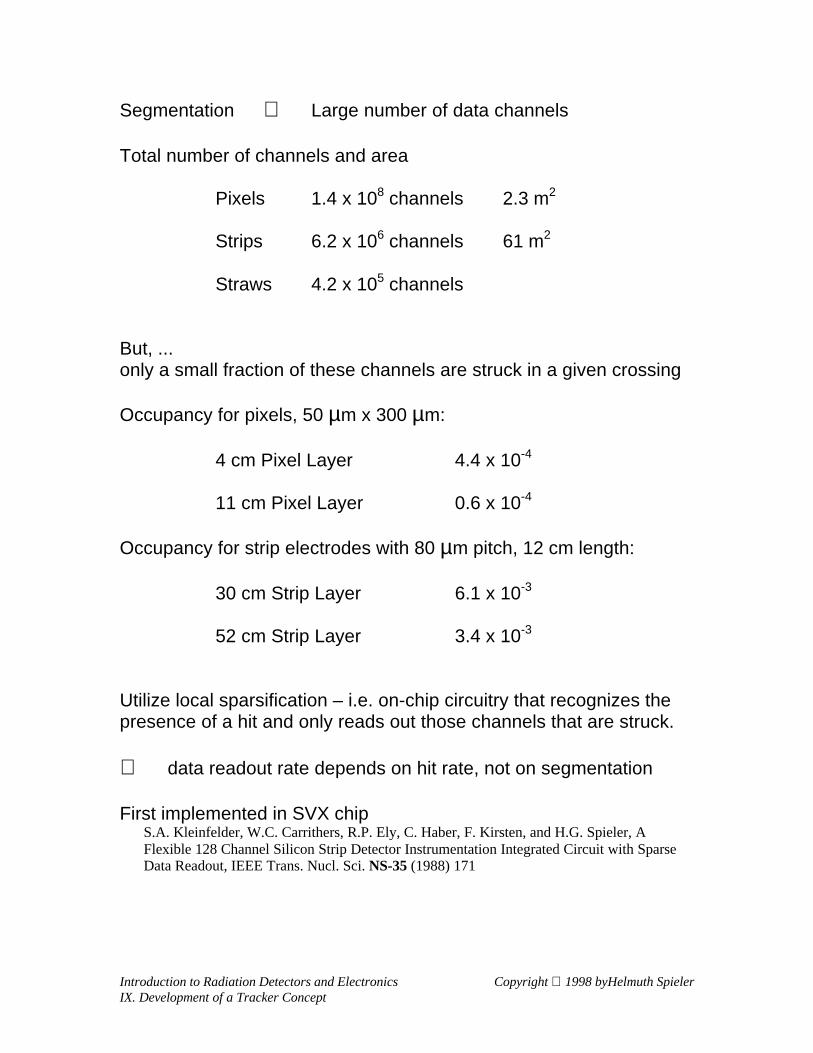
Segmentation ⇒ Large number of data channels
Total number of channels and area
Pixels 1.4 x 10⁸ channels 2.3 m2
Strips 6.2 x 10⁶ channels 61 m2
Straws 4.2 x 10⁵ channels
But, ...only a small fraction of these channels are struck in a given crossing
Occupancy for pixels, 50 µm x 300 µm:
4 cm Pixel Layer 4.4 x 10⁻⁴
11 cm Pixel Layer 0.6 x 10⁻⁴
Occupancy for strip electrodes with 80 µm pitch, 12 cm length:
30 cm Strip Layer 6.1 x 10⁻³
52 cm Strip Layer 3.4 x 10⁻³
Utilize local sparsification – i.e. on-chip circuitry that recognizes thepresence of a hit and only reads out those channels that are struck.
⇒ data readout rate depends on hit rate, not on segmentation
First implemented in SVX chipS.A. Kleinfelder, W.C. Carrithers, R.P. Ely, C. Haber, F. Kirsten, and H.G. Spieler, AFlexible 128 Channel Silicon Strip Detector Instrumentation Integrated Circuit with SparseData Readout, IEEE Trans. Nucl. Sci. NS-35 (1988) 171
Introduction to Radiation Detectors and Electronics Copyright 1998 byHelmuth SpielerIX. Development of a Tracker Concept
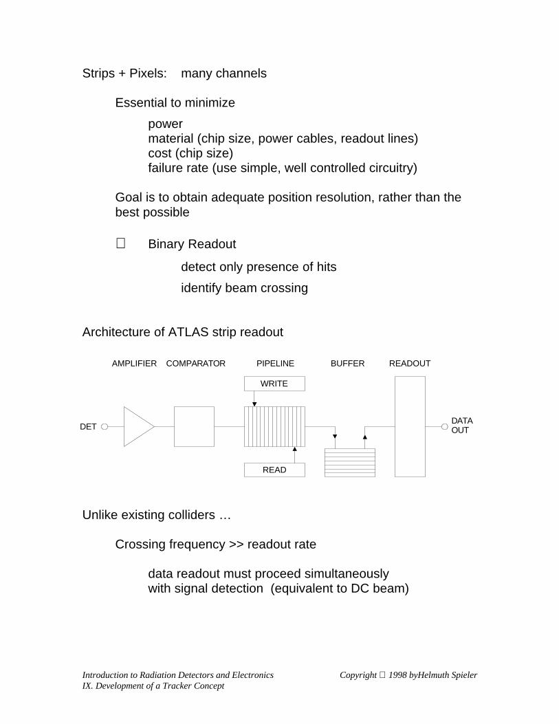
Strips + Pixels: many channels
Essential to minimize
powermaterial (chip size, power cables, readout lines)cost (chip size)failure rate (use simple, well controlled circuitry)
Goal is to obtain adequate position resolution, rather than the best possible
⇒ Binary Readout
detect only presence of hits
identify beam crossing
Architecture of ATLAS strip readout
Unlike existing colliders …
Crossing frequency >> readout rate
data readout must proceed simultaneouslywith signal detection (equivalent to DC beam)
READ
WRITE
DETDATAOUT
AMPLIFIER COMPARATOR PIPELINE BUFFER READOUT
Introduction to Radiation Detectors and Electronics Copyright 1998 byHelmuth SpielerIX. Development of a Tracker Concept
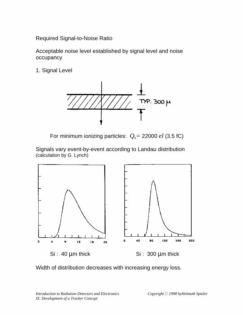
Required Signal-to-Noise Ratio
Acceptable noise level established by signal level and noiseoccupancy
1. Signal Level
For minimum ionizing particles: Qs= 22000 el (3.5 fC)
Signals vary event-by-event according to Landau distribution(calculation by G. Lynch)
Si : 40 µm thick Si : 300 µm thick
Width of distribution decreases with increasing energy loss.

Introduction to Radiation Detectors and Electronics Copyright 1998 byHelmuth SpielerIX. Development of a Tracker Concept
Measured Landau distribution in a 300 µm thick Si detector(Wood et al., Univ. Oklahoma)
The Landau distribution peaks at the most probable energy loss Q0
and extends down to about 0.5 Q0 for 99% efficiency.
Assume that the minimum energy is fLQ0.
Tracks passing between two strips will deposit charge on both strips.If the fraction of the signal to be detected is fsh, the circuit must besensitive signal as low as
0min QffQ Lsh=
Introduction to Radiation Detectors and Electronics Copyright 1998 byHelmuth SpielerIX. Development of a Tracker Concept
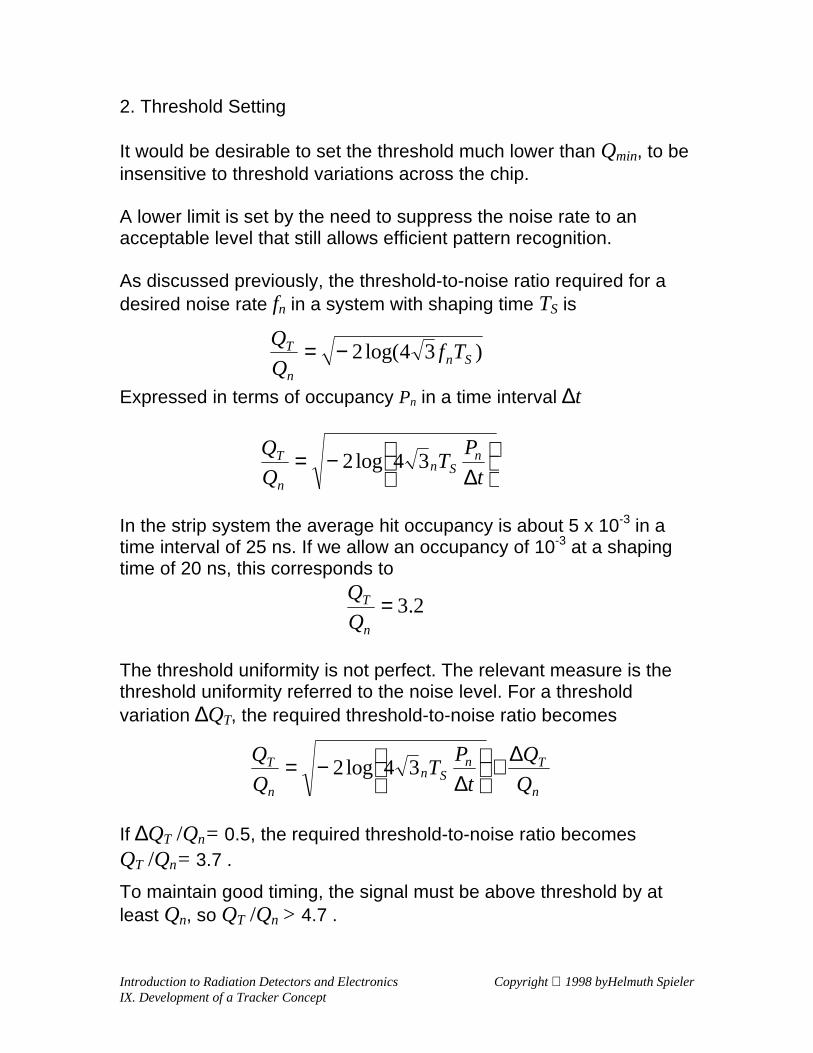
2. Threshold Setting
It would be desirable to set the threshold much lower than Qmin, to beinsensitive to threshold variations across the chip.
A lower limit is set by the need to suppress the noise rate to anacceptable level that still allows efficient pattern recognition.
As discussed previously, the threshold-to-noise ratio required for adesired noise rate fn in a system with shaping time TS is
Expressed in terms of occupancy Pn in a time interval ∆t
In the strip system the average hit occupancy is about 5 x 10⁻³ in atime interval of 25 ns. If we allow an occupancy of 10-3 at a shapingtime of 20 ns, this corresponds to
The threshold uniformity is not perfect. The relevant measure is thethreshold uniformity referred to the noise level. For a thresholdvariation ∆QT, the required threshold-to-noise ratio becomes
If ∆QT /Qn= 0.5, the required threshold-to-noise ratio becomesQT /Qn= 3.7 .
To maintain good timing, the signal must be above threshold by atleast Qn, so QT /Qn > 4.7 .
)34log(2 Snn
T TfQ
Q −=
∆−=
t
PT
Q
Q nSn
n
T 34log2
2.3=n
T
Q
Q
n
TnSn
n
T
Q
Q
t
PT
Q
Q ∆+
∆−= 34log2

Introduction to Radiation Detectors and Electronics Copyright 1998 byHelmuth SpielerIX. Development of a Tracker Concept
Combining the conditions for the threshold
and signal
yields the required noise level
If charge sharing is negligible fsh = 1, so with fL = 0.5, Q0 = 3.5 fC and(QT /Qn )min= 4.7
Qn ≤ 0.37 fC or Qn ≤ 2300 el
If the system is to operate with optimum position resolution, i.e. equalprobability of 1- and 2-hit clusters, then fsh = 0.5 and
Qn ≤ 0.19 fC or Qn ≤ 1150 el
ATLAS requires Qn ≤ 1500 el.
0min QffQ Lsh=
min
0
)/( nT
Lshn QQ
QffQ ≤
min
min
QQQ
Qn
n
T ≤

Introduction to Radiation Detectors and Electronics Copyright 1998 byHelmuth SpielerIX. Development of a Tracker Concept
What type of front-end transistor will provide this noise level atminimum power, bipolar transistor or MOSFET?
Applying the scaling rules outlined previously yields the followingtables (actual noise levels will be ~20% higher):
Total Power of CMOS Front-EndsI(det) ≈ 10-7 A/cm
Qn [el] Power [mW] vs. Strip Length
6cm 8cm 12cm 15cm 18cm1050 2.0 4.01100 1.7 3.31200 1.3 2.6 7.81300 1.1 1.9 5.2 12.01400 1.0 1.5 4.0 7.4 17.2
Total Power of BJT Front-EndsΦ = 1014 cm-2
I(det) ≈ 10-7 A/cm; B=100Qn [el] Preamplifier Current [µA]
vs. Strip LengthPower per Channel [mW]
vs. Strip Length6cm 12cm 15cm 18cm 6cm 12cm 15cm 18cm
1100 20 122 0.61 0.961200 16 75 181 0.59 0.80 1.171300 13 56 101 0.58 0.73 0.891400 11 45 76 126 0.57 0.69 0.80 0.981500 10 37 61 95 0.57 0.66 0.75 0.871600 8 31 50 76 0.56 0.64 0.71 0.80
I(det) ≈ 10-7 A/cm; B=30Qn [el] Preamplifier Current [µA]
vs. Strip LengthPower per Channel [mW]
vs. Strip Length6cm 12cm 15cm 18cm 6cm 12cm 15cm 18cm
1100 24 0.621200 18 0.601300 14 0.581400 12 58 0.58 0.741500 10 43 95 0.57 0.69 0.871600 8.3 34 61 0.56 0.65 0.751700 7.3 29 48 82 0.56 0.64 0.70 0.82
BJT front-ends with a strip length of 12 cm were chosen.

Introduction to Radiation Detectors and Electronics Copyright 1998 byHelmuth SpielerIX. Development of a Tracker Concept
Module Configuration
Two 6 x 6 cm2 detectors are butted edge-to-edge and connected bywire bonds to form a 6 x 12 cm2 detector.
Two of these assemblies are glued back-to-back to form a double-sided detector with 40 mr small-angle stereo.
The strips are on an 80 µm pitch, so each side has 768 channels.
Integrated circuits with 128 ch each are mounted on a ceramic hybrid.
The hybrid is mounted on the detector, to facilitate mounting modulesend-to-end in a row.
The amplifiers are connected to the middle of the detectors to reducethe noise contribution from the resistance of the strip electrodes.
Power and signal connections are made through low-mass Kaptoncables.

Introduction to Radiation Detectors and Electronics Copyright 1998 byHelmuth SpielerIX. Development of a Tracker Concept
Modules will be “shingled” to provide full coverage and overlap tofacilitate relative position calibration.

Introduction to Radiation Detectors and Electronics Copyright 1998 byHelmuth SpielerIX. Development of a Tracker Concept
Some Experimental Results using the CAFE Chip
CAFE Noise Before and After Irradiation
Measured on full-size modules (12 cm strips)
ATT7 and ATT8 use ATLAS baseline detector configuration:
n-strip on n-bulk, AC coupled (fab. by Hamamatsu)
ATT7 detector uniformly irradiated to 1014 cm-2 (MIP equiv)CAFEs irradiated to 1014 cm-2 (MIP equiv)
ATT8 CAFEs from run 2non-irradiated reference module
Noise measured on complete modules (ATT7 at about -10 °C)
Electronic calibration (~ 10% absolute accuracy)
measurement site ATT7chip 0
ATT7chip 1
ATT8chip 0
ATT8chip1
LBNL, 28-Jun-96 1440 el 1380 el 1375 el 1435 el
H8 beam line, 15-Jul-96 1470 el 1380 el 1350 el 1410 el
H8 beam line, 7-Aug-96 1400 el 1375 el 1400 el 1375 el

Introduction to Radiation Detectors and Electronics Copyright 1998 byHelmuth SpielerIX. Development of a Tracker Concept
CAFE Timing Performance
1. Chips from run 1 measured on test boards
• irradiated to 1014 cm-2 (MIP equiv)
Time Walk 16 ns (1.25 - 10 fC) at 1 fC threshold1.25 - 4 fC: 12 ns4 fC - 10 fC: 4 ns
Jitter at 1.25 fC ≈ 4 ns FWHM
Total time diistribution (99% efficiency)confined within about 18 ns.
2. Chips from Run 2 measured on test boards (pre-rad)
Cload= 15 pF, 1 fC threshold, jitter as above
0 2 4 6 8 10 12Input Charge [fC]
0
2
4
6
8
10
12
14
16
Tim
e W
alk
[ns]

Introduction to Radiation Detectors and Electronics Copyright 1998 byHelmuth SpielerIX. Development of a Tracker Concept
Test Beam Data
Tracking Efficiency vs. Occupancy for Full-LengthModules
non-irradiated module
irradiated module (Φ = 1014 cm-2)

Introduction to Radiation Detectors and Electronics Copyright 1998 byHelmuth SpielerIX. Development of a Tracker Concept
Tracking Efficiency and Pulse Height vs. DetectorBias (irradiated, ATT7, and non-irradiated, ATT8)