Embed Size (px)
Citation preview

Development of a FPGA-based True Random Number Generator
for Space Applications
Master thesis in Electronics Systems
at Linköping Institute of Technology
by
Prassanna Shanmuga Sundaram
LiTH - ISY - EX -- 10 / 4398 -- SE
Linköping 2010


Development of a FPGA-based True Random Number Generator forSpace Applications
Master thesis in Electronics Systemsat Linköping Institute of Technology
by Prassanna Shanmuga SundaramLiTH - ISY - EX -- 10 / 4398 -- SE
Supervisor: Dr. László Hinsenkamp
DSI Informationstechnik, Bremen, Germany
Examiner: Dr. Kent PalmkvistISY, Linköpings Universitet
Linköping, 26 February 2010


Division, Department and InstitutionDivision of Electronics SystemsDepartment of Electrical EngineeringLinköpings universitetSE-581 83 Linköping, Sweden
Date : 2010 - 02 - 26
Language
Swedish English
Type of Publication
Licentiate thesis Degree thesis Thesis C level Thesis D level Report
ISBN -ISRNLITH-ISY-EX--10/4398--SE
Series Title and Series number ISSN
Title of series, numbering -URL for Electronic Versionhttp://www.ep.liu.se/
Publication TitleDevelopment of a FPGA-based True Random Number Generator for Space Applications
AuthorPrassanna Shanmuga Sundaram
Abstract
Random numbers are required for cryptographic applications such as IT security products, smart cards etc. Hardware
based random number generators are widely employed. Cryptographic algorithms are implemented on Field
Programmable Gate Arrays (FPGAs). In this work a True Random Number Generator (TRNG) employed for space
application was designed, investigated and evaluated. Several cryptographic requirements has to be satisfied for the
random numbers. Two different noise sources was designed and implemented on the FPGA. The first design was
based on ring oscillators as a noise source. The second design was based on astable oscillators developed on a separate
hardware board and interfaced with the FPGA as another noise source. The main aim of the project was to analyse the
important requirement of independent noise source on a physical level. Jitter from the oscillators being the source for
the randomness, was analysed on both the noise sources. The generated random sequences was finally subjected to
statistical tests.
Keywords
True random number generator, cryptography, random jitter, FPGA, VHDL, ring oscillator, astable oscillator,statistical tests

vi

Abstract
Random numbers are required for cryptographic applications such as IT security products, smart
cards etc. Hardware based random number generators are widely employed. Cryptographic
algorithms are implemented on Field Programmable Gate Arrays (FPGAs). In this work a True
Random Number Generator (TRNG) employed for space application was designed, investigated
and evaluated. Several cryptographic requirements has to be satisfied for the random numbers. Two
different noise sources was designed and implemented on the FPGA. The first design was based on
ring oscillators as a noise source. The second design was based on astable oscillators developed on
a separate hardware board and interfaced with the FPGA as another noise source. The main aim of
the project was to analyse the important requirement of independent noise source on a physical
level. Jitter from the oscillators being the source for the randomness, was analysed on both the noise
sources. The generated random sequences was finally subjected to statistical tests.
vii

viii

Acknowledgements
This work was carried out at DSI Informationstechnik GmbH, Bremen, Germany. I am deeply
indebted to my supervisor Dr. László Hinsenkamp for giving me permission to commence this
thesis work at their organization. I would like to thank him for his support, guidance,
encouragement and stimulating suggestions that has helped me a lot throughout this project. Many
thanks to all the employees at DSI for their support and always keen to help me whenever needed. I
would like to thank Tiby and Alex for their support in this project. I would also like to thank
Sebastian, Stefan and Olaf for their suggestions when I designed the PCB.
My sincere gratitude to my examiner Dr. Kent Palmkvist at Linköping University who has
supported me on this thesis work. I am grateful and indebted to my parents for their constant
support and prayers. Thanks to my friends and gratitude to everyone in completing this thesis.
ix

x
Table of Contents
1. Introduction.....................................................................................................................................1 1.1 Problem Description.................................................................................................................1 1.2 Project Goals ............................................................................................................................2 1.3 Redundancy for Space Applications.........................................................................................3 1.4 Radiation effects.......................................................................................................................4 1.5 Thesis Outline...........................................................................................................................5
2. RNG Basics and Construction.........................................................................................................7 2.1 Classification of Random Number Generators.........................................................................7 2.2 Architecture for a TRNG..........................................................................................................8
2.2.1 Noise Source..................................................................................................................10 2.2.2 Sampler..........................................................................................................................10 2.2.3 Post Processing..............................................................................................................10 2.2.4 Statistical Tests..............................................................................................................11
2.3 Types of TRNG Designs ........................................................................................................11 2.3.1 Baggini and Bucci ..........................................................................................................11 2.3.2 The Intel TRNG Design..................................................................................................12 2.3.3 The Tkacik TRNG Design .............................................................................................13 2.3.4 The Epstein et al. TRNG design ....................................................................................13 2.3.5 Fischer Drutarovsky Design ...........................................................................................14 2.3.6 The Golic FIGARO Design ...........................................................................................15 2.3.7 Kohlbrenner Gaj Design ................................................................................................15 2.3.8 The Rings Design............................................................................................................16 2.3.9 The Dichtl and Golic Design..........................................................................................17
3. TRNG Ring Design and Interaction .............................................................................................19 3.1 Tools and Hardware ...............................................................................................................19
3.1.1 Spartan 3-E Evaluation Board.........................................................................................19 3.1.2 Oscilloscope and Probes.................................................................................................20
3.2 FPGA and Cryptography........................................................................................................20 3.3 Ring Design............................................................................................................................21
3.3.1 Simple Ring Oscillator....................................................................................................21 3.3.2 Two Rings ......................................................................................................................21 3.3.3 Design with Multiple Rings............................................................................................22
3.4 Test for Independence with Correlation of the signals ..........................................................24 3.4.1 Long Oscillator Interaction.............................................................................................24 3.4.2 Design Implementation Mapping Place& Route............................................................25 3.4.3 Auto Placement of Rings................................................................................................26 3.4.4 Manual Placement of Rings............................................................................................28
3.5 Data Analysis - Correlation ..................................................................................................31 4. Jitter Analysis................................................................................................................................37
4.3 Jitter Measurements.................................................................................................................384.4 Jitter in Ring Oscillators .........................................................................................................38
4.4.1 Incremental Jitter Accumulation Model..........................................................................39 5. Sampling Techniques and Interface..............................................................................................43
5.1 Sampling ................................................................................................................................43 5.2 Restart Techniques..................................................................................................................44
xi

5.3 Post Processing ......................................................................................................................46 5.3.1 XOR corrector and Von Neumann Corrector.................................................................47 5.3.2 Resilient Functions..........................................................................................................47
5.4 Interface..................................................................................................................................48 6.Oscillator Board Design ................................................................................................................51
6.1 Astable Oscillator ..................................................................................................................52 6.2 Circuit Design ........................................................................................................................54
6.2.1 Different Oscillating Frequencies...................................................................................55 6.3 Schematic design ...................................................................................................................56 6.4 PCB Layout.............................................................................................................................57 6.5 Correlation and Jitter Analysis...............................................................................................59 6.6 PCB Evaluation Board Interface.............................................................................................61
7. Statistical Tests and Analysis .......................................................................................................63 7.1 NIST Test Suite......................................................................................................................63
7.1.1 Frequency Test (Mono Bits Test)...................................................................................64 7.1.2 Frequency Test within a Block.......................................................................................64 7.1.3 Runs Test.........................................................................................................................64 7.1.4 Test for the Longest Run of Ones in a Block..................................................................64 7.1.5 Serial Test.......................................................................................................................64
7.2 BSI Test Suite.........................................................................................................................65 7.2.1 Functionality classes of AIS 31......................................................................................65 7.2.2 Class P1 ..........................................................................................................................66 7.2.3 Class P2...........................................................................................................................67
7.3 Statistical Tests on TRNGs.....................................................................................................68 8. Conclusion ....................................................................................................................................71A. Appendix : A.1 AIS 31-BSI Statistical Tests .............................................................73A.2 Measurements .............................................................................................................................75A.3 FPGA Editor Routed Design.......................................................................................................77A.4 PCB Schematic............................................................................................................................78A.5 PCB Picture.................................................................................................................................79 9.Bibliography...................................................................................................................................80Abbreviations.....................................................................................................................................82
xii
1. Introduction
1. Introduction
Cryptography is a set of techniques for hiding information. It is employed in several fields as part of
security protocols to secure classified information and data. Communication, being an integral part
of life, including the internet and other means of communication has given rise to security threats.
Cryptography thus provides the necessary protection from the threats by protecting the data, i.e.
providing different means and methods of converting data into an unreadable form. The basic aim
of cryptography is that the data should not be accessed by an unauthorized user. The content of the
data frames should be hidden. Another application is to ensure that the data must always be
acknowledged by the originator of the message.
Cryptographic applications require random numbers to operate. There are many random number
generation schemes, and Random Number Generators (RNGs) are actively used as IT security
products. The random numbers generated should be truly random, else they can significantly
weaken the security system. They must not be predictable. They must be uniformly distributed on a
given range and independent of each other. Thus there is a need for an ideal RNG that satisfies all
these constraints, although its development involves more mathematical analysis [1].
Space applications must employ highly sophisticated security elements. Random number generators
are employed in satellite systems both at the base station as well as on the satellites. Highly secured
encryption and decryption is employed in all the communications with the satellite from the base
station. The cryptographic key is generated and, once it is used, the generated key should be
destroyed to ensure it is not used any more.
Random number generators can be developed using Field Programmable Gate Arrays (FPGAs).
The ported designs on the FPGAs can be employed as a part of the space applications. There are
several requirements that have to be considered when the device is to be placed in space. These are
radiation effects, as well as the life cycle of the system in order to have a redundant system which
improves the reliability of the entire device.
1.1 Problem Description
The Random number generator has to be designed with a good cryptographic quality and it must
also be considered that it is being developed for a space application. Cryptographic quality is
achieved by random numbers that satisfy the requirements of cryptographic algorithms.
1

1. Introduction
An FPGA-based design has to be implemented. The noise source which is the basic random source
for any key generator is to be implemented in the FPGA and a secondary design using a separate
hardware board. The most important quality of statistical independence should also be checked
while implementing the design. There are different types of random number generators such as true,
deterministic etc. We have selected a True Random Number Generator, TRNG. A TRNG is a
physical device that ensures unbiased bits and statistical independence. It will harvest the
randomness in the underlying physical source and the generator will have no internal state kept.
Such a design also ensures high throughput to area ratio [4]. It also produces a reliable bit rate [5].
Once the random sequence is generated, it is subjected to statistical tests to test its quality.
1.2 Project Goals
The project aims to satisfy two different constraints.
• Cryptographic Quality
• Space Quality
Cryptographic QualityA cryptographically strong random sequence has to be generated. In order to achieve this the quality
of the random numbers should satisfy two requirements
• Random numbers must not be predictable i.e. statistically independent.
• Statistical homogeneity.
The knowledge of subsequences of random numbers shall not enable the computation of
predecessors or successors or to guess them with non-negligible probability. The random numbers
should have all possible values with equal probability and should also be independent from
predecessors and successors [1].
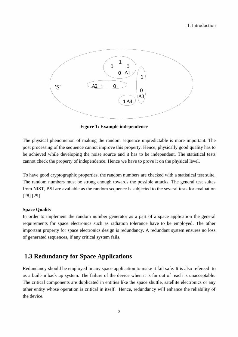
IndependenceIndependence occurs when knowing an event that does not change the probability of another event.
[15]. The definition of independent probability is given by
P(A1, A2, …An) = P(A1)P(A2) …P(An)
where the joint probability of all of the events occurring equals the product of the individual
probabilities.
Consider the example as shown in figure 1, the sample space 'S' has several points, bits which has a
probability among each other. The events A1,A2,A3,A4 are defined by individual sets. Thus it can
be verified that A1 and A2 are independent by P(A1 ∩ A2) = P(f) = P(A1) P(A2)., where P(f) is the
probability function. Similarly A1 and A3 are independent, A2 and A4 are independent and so on.
2
1. Introduction
Figure 1: Example independence
The physical phenomenon of making the random sequence unpredictable is more important. The
post processing of the sequence cannot improve this property. Hence, physically good quality has to
be achieved while developing the noise source and it has to be independent. The statistical tests
cannot check the property of independence. Hence we have to prove it on the physical level.
To have good cryptographic properties, the random numbers are checked with a statistical test suite.
The random numbers must be strong enough towards the possible attacks. The general test suites
from NIST, BSI are available as the random sequence is subjected to the several tests for evaluation
[28] [29].
Space QualityIn order to implement the random number generator as a part of a space application the general
requirements for space electronics such as radiation tolerance have to be employed. The other
important property for space electronics design is redundancy. A redundant system ensures no loss
of generated sequences, if any critical system fails.
1.3 Redundancy for Space Applications
Redundancy should be employed in any space application to make it fail safe. It is also refereed to
as a built-in back up system. The failure of the device when it is far out of reach is unacceptable.
The critical components are duplicated in entities like the space shuttle, satellite electronics or any
other entity whose operation is critical in itself. Hence, redundancy will enhance the reliability of
the device.
3
000
1
01
1
0
1A1
A3
A2
A4
'S'

1. Introduction
Usually, the redundancy is implemented with more operating elements or functional paths as it
becomes difficult to maintain the system functionality of the device. It is achieved by the
combination of hardware and software elements [2].
Regarding the hardware aspects, adding redundancy implies that the space, weight, complexity and
power consumption increases. It is one of the solutions for complex electronic systems for Space
applications [2]. Finally we have to assess the advantages and disadvantages of redundancy before
its implementation. Different application oriented approaches are available to improve the reliability
with a redundant design. There are in general two types of redundancy.
1. Active Redundancy, does not require an external component if any part of the device fails.
2. Standby redundancy, requires an external component to detect, make a decision, and then to
switch to another element or a different path in order to serve as a replacement for the failed
element.
1.4 Radiation effects
Radiation effects in space have to be considered for any electronic component to be placed on a
satellite. Radiation is a term that describes energy or matter moving through space. Sunlight is a
form of electromagnetic radiation, ultraviolet, gamma and infrared are some of the common types
of radiation [3],[30]. Cosmic rays produce cosmic radiation which are described as fast moving
particles of matter. The cosmic rays travel at nearly the speed of light. They are nuclei of atoms
such as hydrogen, helium, iron and other forms which travel through space at hundreds of
thousands of kilometres per second. Another form of radiation which is not formed of light or
matter, is neutrino radiation. Neutrinos are particles that travel at the speed of light, same as that of
an electromagnetic radiation, yet they are not made of matter and also are not produced from
electric or magnetic fields. All our electronic components have to survive in severe conditions and
hence the design of such electronics is a huge area to explore and is done with the utmost care.
Radiation tolerant FPGAs are widely employed in satellites and aerospace applications. These offer
the designers with features from high performance to low power consumption and wide array of
choices for space electronics without sacrificing radiation tolerance and reliability [34].
4

1. Introduction
1.5 Thesis Outline
Chapter 2 introduces True Random Number Generator basics, construction and the different types.
Chapter 3 gives the rings design for the TRNG, the experiments for ring design and statistical
independence analysis. Chapter 4 discusses more about the independence of the rings and describes
the analysis with MATLAB as well as the random jitter with timing issues for the constructed
sources of the TRNG. Chapter 5 gives the sampling techniques method for restarting the rings.
Chapter 6 discusses the Astable Multivibrator oscillator that was designed with descriptions of
construction, simulation and PCB manufacture. Chapter 7 discusses more about the statistical tests
and the tests performed for the designs. Chapter 8 gives the conclusion and future scope of this
project.
5

6

2. RNG Basics and Construction
2. RNG Basics and Construction
A random number generator (RNG) has to be developed by employing an appropriate design and
then implementing it suitably. The second task is more difficult since it has to be assured that the
implemented design is secure.
2.1 Classification of Random Number Generators
The RNGs are classified as deterministic and true or non-deterministic types. Deterministic types
are termed as Deterministic Random Number Generators (DRNGs) which generate pseudo random
numbers algorithmically. The second type are termed as True Random Number Generators
(TRNGs) [1]. Figure 2 shows a classification method for RNGs [1].
RNG
Deterministic True, Non-Deterministic
Pure Hybrid
Physical Non- Physical
Pure Hybrid Pure Hybrid
Figure 2: RNG classification
7

2. RNG Basics and Construction
True random number generators are further classified into physical (PTRNGs) and non-physical
(NPTRNGs). The physical ones use non-deterministic effects such as electronic noise from diodes,
thermal noise, and free running oscillators as the source of randomness. They may also derive noise
from physical experiments such as time of emissions from radioactive decay, quantum random
process etc. The NPTRNGs derive noise from deterministic effects such as system time, hard disk
seek time, RAM content, user interaction etc. The next classification is that of hybrid RNGs which
would have the qualities of both DRNGs and TRNGs. Hence the TRNGs will have the security
reliability based on unpredictability of their output, while that of the DRNGs will depend on the
computational complexity of possible attacks [1]. Hybrid RNGs will have design elements from
both DRNGs and TRNGs while the pure RNGs exhibit physical, non-physical and deterministic
properties respectively. The security of the hybrid RNGs are based upon deterministic and non-
deterministic parts respectively.
TRNGs that are classified as physical and non-physical can be formed as hardware-based and
software-based generators respectively. An important fundamental property of the TRNG is its
entropy source. Entropy is a measure of the uncertainty that is associated with a random variable.
Hence, for a software based generator, the entropy source is based on random events in a computer
system that can be captured using software procedures. These include mouse movements and clicks,
keystrokes, the system clock, the content of input and output buffers, operating system values such
as system load and network statistics [4]. Usually, the entropy is high for the hardware-based
generators while the statistical property requirements of the generator would also be satisfied.
2.2 Architecture for a TRNG
The general architecture of a TRNG consists of three parts; the noise source constituting analog
part, the post-processing and external interface makes up the digital part. The later is used to send
the generated bits to the desired application such as smart cards, etc. Figure 3 and 4 illustrates the
generic design and the architecture of a TRNG. The noise source generates the time continuous
analog signals that are digitized to binary values. The digitized analog signal (DAS) represents the
random numbers. The DAS is then algorithmically post-processed to yield internal random numbers
to reduce the potential weakness by digital correction. The data compression techniques would
lower the output rate of the RNG so the post processing has to be done carefully without losing the
necessary bits [5]. In some cases when there is a strong noise source, the post processing is not
necessary as the noise source produces non-predictable sequences [4]. The common modes of
correction schemes are XOR corrector or Von Neumann Corrector [23]. Once the correction is
done, the bits are sent to the desired storage using the external interface for further analysis and
statistical tests.
8

2. RNG Basics and Construction
Analog Digital External Interface
digitized analog signal internal external
DAS - random number random no. random no.
Figure 3: Generic design of a TRNG
Analog
Digital
External
Random Bits
DAS - random no internal
random no
Figure 4 : Architecture of a TRNG
9
Noise Source Algorithmic Postprocessing
Noise Source Sampler Postprocessing
(Digital Correction)
Buffer
Output Interface
StatisticalTests
2. RNG Basics and Construction
2.2.1 Noise Source
There are several types of noise sources employed in TRNGs. The entropy source for the TRNG
has the physical source of randomness [5].
• Electronic noise is the thermal noise or Johnson noise that is generated by the thermal
agitation of the electrons in a conductor. The thermal noise can be observed from the
resistors.
• Quantum mechanical properties from the nuclear decay of radioactive elements can also be
used as a form of noise source.
• Shot noise is generated from the voltage difference or alternatively, the potential barrier,
from the travelling electron holes. Examples of such noises are from zener diodes or
avalanche diodes that produce the breakdown voltages.
• Metastability is another property which is achieved when the flip flops setup and hold
conditions change. The gates are cross-connected which leads to unpredictable operation
and different oscillations, producing unpredictable logic highs and lows.
• Jitter can also be used as a noise source, when the timing edges raise and fall times of a
signal are irregular. Jitter can be categorised into deterministic and non-deterministic types.
Peak to peak jitter, sinusoidal jitter, data-dependent jitter and uncorrelated jitter are a few
other types.
2.2.2 Sampler
The sampler performs the necessary sampling of the noise signal and can be called the harvesting
mechanism for the physical noise source. It produces the digitized form of the analog signal.
Usually a D-type flip-flop is used as the sampler. Voltage controlled oscillator (VCO) is also used
for some types of noise sources.
2.2.3 Post Processing
Post-processing is usually performed to increase the randomness of the signal. The values of the
signal which has been post-processed, would have a uniform distribution when compared to the raw
random bits. The entropy per DAS random number will be increased. Depending upon the post-
processing algorithm, the security of the generator is increased [4]. The different types of post-
processing algorithm that are implemented are XOR correction, Von Neumann correction, extractor
function, hash function, resilient functions, etc. [5] [6].
10
2. RNG Basics and Construction
• Cryptographic Hash Functions: The most popular and robust post-processing technique,
implemented by running the output of the TRNG design through a cryptographically strong
hash function such as SHA-1 or MD5. The Intel RNG used SHA-1 [6].
• Von Neumann Corrector: The oldest and simplest method of post-processing. It eliminates
the localized biases of the bit stream. The bit rate is reduced by 1/4 of the input bit rate [23].
• Extractor Functions: These were proposed to make TRNG designs more robust against
changing environmental conditions. The extractor functions are powerful stateless functions
with quantifiable properties.
• Resilient Functions: Filters away the deterministic bits. The deterministic bits that are
affected can be used to study the tolerance property of the resilient functions. Higher
resiliency degree of the resilient function and the number of deterministic bits expected in a
sampling window quantifies the tolerance of the TRNG to active adversaries [7].
2.2.4 Statistical Tests
The statistical tests were performed to check the sequence of random bits that were generated. The
two most important standards for the test units are from NIST, National Institute of Standards and
technology from the U.S.A. and BSI, Bundesamt für Sicherheit in der Informationstechnik from
Germany. The random bit sequence has to successfully pass the desired test to verify that the
developed TRNG is secure.
2.3 Types of TRNG Designs
In this section few TRNG designs are discussed. Though there are many more designs which are
patented and are typically used for commercial purposes.
2.3.1 Baggini and Bucci
This design introduced by Baggini and Bucci includes a combination of analog and digital
components as shown in figure 5 below.
11

2. RNG Basics and Construction
Figure 5 : Baggini and Bucci TRNG design
The design is resistant to variations in operating conditions and component behavior. It is more an
analytical model of the TRNG which captures the relationship between the maximum bit correlation
to the output bit rate [8].
2.3.2 The Intel TRNG Design
The Intel TRNG design is shown in Figure 6. The design is made up of two resistors as a noise
source, which drives the Voltage controlled oscillator. These resistors are provided with the
differential configuration to make the design more robust against power supply and environmental
variations. The drift in the low and high oscillation frequencies, results in the random binary digits.
The VCO is sampled by another oscillator and the resulting signal is post processed by the Von
Neumann corrector. It is also corrected using the hash function SHA-1. The design passes the NIST
FIPS 140-1 tests and also produces a strong sequence [6].
Figure 6: Intel random number generator
12
VCO
OSC
Latch Corrector
Thermal Noise
Amplifier
High SpeedOscillator
Voltage Controlled Oscillator
Low frequency oscillation
High frequency oscillation
/N
DFF/2
Clk
Pulse generator
Comparator /w hysterisis
Holding Capacitance
Sampling Switch
Low pass filter
Noise Source
Sampler
2. RNG Basics and Construction
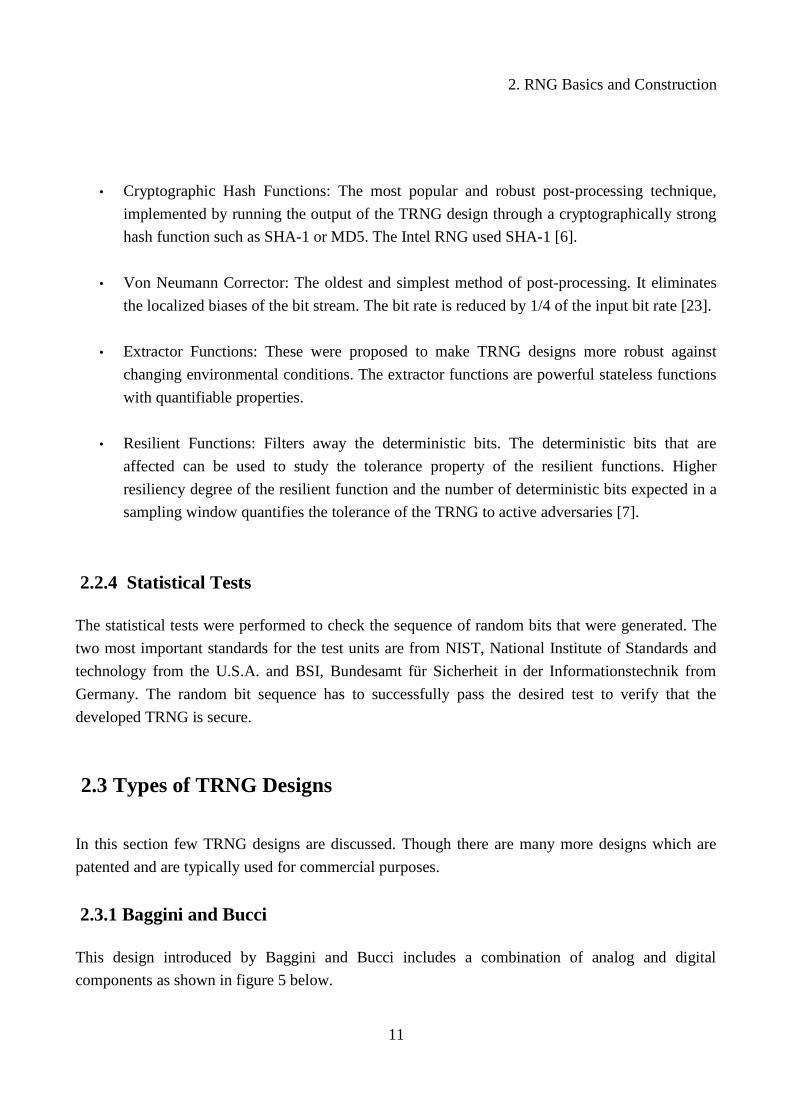
2.3.3 The Tkacik TRNG Design
The Tkacik design randomly samples the XOR of bits chosen from a Linear Feedback Shift
Register (LFSR). This TRNG outputs 32 bits at a time. The jitter from the oscillator circuits forms
the source of randomness [9]. The output sequence was verified by using NIST 140-1 and Crypt X
test suites. It is claimed to have good statistical behavior [9]. However, the source of entropy is
limited as only two oscillators are used. It is also said that if the output rate was lowered or a non
linear component was included, it would make the design more robust. However, it has been
criticized by Dichtl [10] for potential weaknesses. This design uses an LFSR as a source and an
attacker could build a linear model to solve it.
Figure 7 : Tkacik design
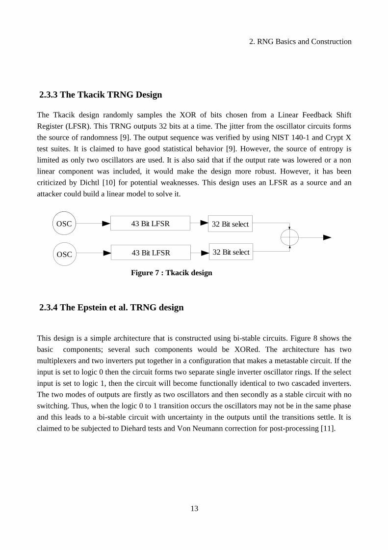
2.3.4 The Epstein et al. TRNG design
This design is a simple architecture that is constructed using bi-stable circuits. Figure 8 shows the
basic components; several such components would be XORed. The architecture has two
multiplexers and two inverters put together in a configuration that makes a metastable circuit. If the
input is set to logic 0 then the circuit forms two separate single inverter oscillator rings. If the select
input is set to logic 1, then the circuit will become functionally identical to two cascaded inverters.
The two modes of outputs are firstly as two oscillators and then secondly as a stable circuit with no
switching. Thus, when the logic 0 to 1 transition occurs the oscillators may not be in the same phase
and this leads to a bi-stable circuit with uncertainty in the outputs until the transitions settle. It is
claimed to be subjected to Diehard tests and Von Neumann correction for post-processing [11].
13
OSC
OSC
43 Bit LFSR
43 Bit LFSR
32 Bit select
32 Bit select
OSC

2. RNG Basics and Construction
Figure 8: Bi-stable memory Epstein TRNG design
2.3.5 Fischer Drutarovsky Design
The design samples the jitter in a phase locked loop (PLL) on a specialized reconfigurable platform.
The speciality of this design is that it was the first such random number generator design targeted
mainly for FPGAs [12]. It was implemented using the built-in PLL of an Altera FPGA. The PLL
was then sampled using delay cascaded samplers.
Figure 9 : Fischer Drutarovsky model
There are multiple samplers for this design and they are able to sample near the transition zone that
is influenced by the jitter. They are then XORed and then again the output is downsampled using a
decimator. They claim an output bit rate of about 70 Kbits/s [12]. The output sequence was tested
using the NIST test suite.
14
VCO1/n 1/k
1/v1/mClock Shift Circuitry
FIN m/(n*k)
FIN m/(n*v)
FIN
Phase comparator
.
Out In1
In2
sel
Out In1
In2
sel
Select
.
Oscillator Output

2. RNG Basics and Construction
2.3.6 The Golic FIGARO Design
The fibonacci oscillator, as it is named, has a structure that resembles the LFSR except for the delay
elements being replaced by inverters. There are switches in between the feedback positions as
denoted by 'fi'. If f i = 1 then the switch is closed else it is open. The switching values are
represented by a feedback polynomial [10].
f x =∑i=0
r
f i x i where fo= fr=1 ( 1 )
Figure 10 : Fibonacci oscillator architecture
2.3.7 Kohlbrenner Gaj Design
This design uses the jitter in the ring oscillators as the entropy source [4]. It was designed as a
perfect match to the configurable logic blocks (CLB) architecture of a Xilinx Virtex II FPGA. The
output of the two latches is routed externally from the CLB outputs back to their inputs as two
feedbacks. The oscillator frequency is determined by the delay elements in the oscillator path. The
path is through two look up tables, four multiplexers and two memory cells. It is claimed to be
stable up to 130 Mhz [4]. Figure 11 shows the oscillator CLB structure of the Kohlbrenner Gaj
design.
15
...
f 1 f 2 f r-1
Oscillator Output

2. RNG Basics and Construction
Figure 11: CLB structure - Kohlbrenner Gaj design
2.3.8 The Rings Design
The rings design was proposed by Sunar, Martin and Stinson [5]. It is a simple design, which has
free running oscillators being combined by an XOR and then sampled. There is a detailed
mathematical model for the proposed design [5]. The design was developed on a Xilinx Virtex II
FPGA. It produces a 2.5 Mbps bit rate and a sampling frequency of around 40 MHz. The design
consists of 110 rings with over 13 inverters each. In order to reduce the number of rings, resilient
functions should be used for post-processing of the TRNG. The resilient functions are developed
from linear cyclic code. The Diehard and NIST tests were performed on the generated sequence.
The major criticism of this design is the statistical independence assumption of the ring oscillators
by the publication from Dichtl and Golic [10]. Another characteristic of the design is the careful
placement of the rings for interaction analysis. The phase interlock of the designs contributing to
reduce the fill rate are analysed in detail in [10] [18]. Figure 12 illustrates the design.
16
Oscillator Output
A4A3A2A1
A4A3A2A1
LUT1
LUT2
D
DD
D
Q
QG
G
R
R
Feedback 1
Feedback 0
Enable
Reset
2. RNG Basics and Construction
Figure 12. Rings oscillator design
2.3.9 The Dichtl and Golic Design
The Ditchtl and Golic design is the same as the Fibonacci and Galois ring oscillator as described in
section 2.3.6. It is mainly derived by using a restart technique. The oscillators are restarted from the
initial condition. The time that it takes to observe a random bit after it is restarted, is the sampling
rate and throughput of the generator. It produces a throughput of about 6.25 Mbps. It is also claimed
to produce high entropy rates and is often employed in embedded systems [23].
The different RNG designs was presented along with the basics of the architecture and construction
of TRNGs.
17
...
...
...
D Q
fs
Ψ 2
Ψ 1
Ψ r
Ψ

18

3. TRNG Ring Design and Interaction
3. TRNG Ring Design and Interaction
The TRNG construction starts with the noise source design. The noise source for our
implementation was developed using ring oscillators. The design and different experiments which
were carried out as part of the rings design is presented.
3.1 Tools and Hardware
The design was developed using Xilinx ISE Foundation 10.1 and was coded in VHDL. The Xilinx
ISE Foundation developed by Xilinx Inc. facilitates a full implementation chain from establishing
the system design to programming it with blocks or schematic entry, synthesizing the design,
translating, mapping, placing and routing and finally implementing the design on the desired FPGA
board. The simulation of the design was carried out using the ModelSim simulator integrated into
the ISE tool. It allows us to create a hierarchical level design entry with the highest level on the top
and the secondary design level entries as blocks interconnected using buses.
3.1.1 Spartan 3-E Evaluation Board
The design was implemented on one of the Spartan series FPGA boards from Xilinx, the Spartan
3-E Evaluation board incorporating a XC3S500E-5fg320 device. The Spartan 3-E series FPGAs are
regarded as being high volume cost sensitive application targets. Though the FPGAs that are used
for space applications are expensive to use, this work mainly focuses on development on the
Spartan 3E board in order to investigate the designs and run tests on their behaviour.
Some of the key features of the Spartan 3-E board are [13] :
• multi-standard I/O pins and differential I/O.
• System gates numbering about 500K
• DDR SDRAM support up to 333 Mb/s
• Densities up to 10,476 logic cells, including optional shift register or distributed RAM
support.
• A number of distributed RAM 73K bits.
• 4 Digital Clock Managers (DCMs) and a high frequency range (5 to 300 Mhz).
• 360K bits Block ram.
• 20 Multipliers.
19

3. TRNG Ring Design and Interaction
• IEEE 1149.1/1532 JTAG programming/debug port.
• 232 User I/O pins and 92 Maximum differential I/O pins.
The general components that are available on the evaluation board are [14].
• Slide switches, Push buttons, Rotary knob for necessary tests.
• On-board 50 Mhz clock.
• Character LCD screen.
• VGA, RS232, PS/2 ports.
• DAC and ADC.
• Expansion connectors, etc.
3.1.2 Oscilloscope and Probes
The measurement of the signals from the design were carried out using the Tektronix DPO4104
digital oscilloscope. Some of the key features of this oscilloscope are up to 1 GHz bandwidth
measurement, sampling up to 5 GS/s, record length of up to 10 M points and 4 channels of
operation.
The probes that were used to measure the signals were Tektronix Active probes with up to 1.5 GHz
probe bandwidth and Tek passive voltage probes of up to 500 MHz bandwidth.
3.2 FPGA and Cryptography
FPGAs as a reconfigurable devices have been employed for implementing cryptographic algorithms
for quite a long time [4]. FPGAs are flexible in terms of programming and implementation of
several algorithms and functions. They are widely used in research of crypto applications. FPGAs
provide performance flexibility and benefits compared to application specific integrated circuit
(ASICs). Traditionally, ASICs was used more for the cryptographic implementations [12]. Later,
due to greater flexibility and reprogrammability, it have become easier to modify algorithms and
program them on FPGAs. The development of an algorithm is faster and allows for a shorter time to
market on an FPGA.
20

3. TRNG Ring Design and Interaction
FPGAs consist of CLBs that includs flip-flops and lookup tables that are used to implement the
arbitrary functions. The netlist is implemented by the lookup tables and flipflops, multipliers,
blocks of RAM, PLL, DLL and several IP cores and processor cores. The interconnection of the
elements is defined by hardware programming languages such as VHDL or Verilog. The ISE tool
would convert the description into a bitstream which is then sent to the FPGA. The size of the
configuration bitstream ranges from Kbits to Mbits depending upon the size of the design on the
FPGA.
3.3 Ring Design
The noise source, as discussed earlier, is designed in the form of a ring oscillator. A ring oscillator
is usually designed by connecting an odd number of inverters (NOT gates) together. The output of
the last inverter is connected back to the input as a feedback. The output will oscillate between two
voltage levels representing the true and false logic states.
3.3.1 Simple Ring Oscillator
Figure 13 illustrates a simple 3 stage ring oscillator. The odd number of counts results in a self
oscillating mode.
Figure 13: Simple ring oscillator
3.3.2 Two Rings
Two three-inverter oscillators are connected together and their output XORed and generating an
output sequence as illustrated in figure 14. The ring oscillators are used in the development random
number generators as they are simple to design [12].
21

3. TRNG Ring Design and Interaction
Figure 14: Two rings XOR'ed
Similar to the two rings, several rings with different ring lengths, namely 7-11, 11-13, 13-17 etc.,
can be used as the noise source of the TRNG.
3.3.3 Design with Multiple Rings
A multiple ring-based design was developed with several ring oscillators with different ring lengths.
The rings were designed with the lengths of 7,11,13,17,19 inverters each. Each ring was replicated
40 times amounting to a total of 200 rings. The 200 rings are XORed together to generate the output
signal. The rings are asynchronous to each other, and thus they are not clocked in this part of the
design. Figure 15 shows the multiple ring design. Symbol 'I' represents the length of the ring
according to the number of inverters and 'k' represents the number of rings in total. The period
usually depends on the number of inverters used and the delay of each inverter. The jitter generated
by each oscillator accounts for the randomness of the signal. The output from the XOR would be an
analog signal. It should be sampled, clocked to convert it to a digital signal. The output signal
consists of the periodic transitions of all the included 200 rings. The XOR output will oscillate in
the range of 150 to 200 MHz. The design was coded in VHDL and implemented on the Spartan 3-E
FPGA evaluation board. The output was driven through the I/O pins on the evaluation board and
measured on a Tektronix Oscilloscope.
22
Output Sequence

3. TRNG Ring Design and Interaction
Figure 15 : Multiple ring design - ring 200
23
k=41
k=81 k=120
...
Output 200 Parallel Rings group
k=1 k=40
k=80
k=121 k=160
k=161 k=200
I=7 I=11 I=13 I=17 I=19
...
...
...
...
40 rings each – 7,11,13,17,19 Inverters

3. TRNG Ring Design and Interaction
3.4 Test for Independence with Correlation of the signals
The correlation of the signals from ring 200 and a new ring with 27 inverters was investigated. The
test for independence was performed at the output from the noise source before it is sampled, refer
to figure 4. The signal outputs from the noise source of two separate rings was analysed. Two
events are said to be statistically independent if
P(A1 ∩ A2) = P(A1)P(A2) ( 2 )
where P(A) is the probability of event A occurring. Events are said to be independent if joint
probability is equal to the product of their individual probabilities. The left side of the above
equation represents the AND operation and the right hand side of the equation represents algebric
multiplication. In our analysis the physical level independency is analysed and not the events as
show in equation 2.
In the design that is implemented, the transitions of the signal after XORing them should be
checked for independence. It has to be seen if it is independently distributed over a period of time.
Ring oscillators placed on the same FPGA chip would have interactions between each other which
have to be tested.
3.4.1 Long Oscillator Interaction
To test the design, a separate noise source with a relatively long ring oscillator was implemented.
This noise source has to be realized along with the present design of 200 rings on the FPGA. Once
the two sets of rings were developed, they were implemented on the FPGA and tested for
interactions by observing the signals on the oscilloscope. Figure 16 illustrates a 27-inverter ring
oscillator which is a new source.
Figure 16 : Ring 27 oscillator
24

3. TRNG Ring Design and Interaction
3.4.2 Design Implementation Mapping Place& Route
Once the design was coded in VHDL, steps in synthesizing the design, translating, mapping,
placing & routing and finally programming it to the FPGA was carried out. Before the design is
implemented, we can constrain the design by certain timing requirements. We can specify the
mapping, block placement and timing specifications. Mapping can specify a particular block of
logic to be implemented as a CLB.
Once the design is entered, simulation is performed before implementation. A functional simulation
tests the logic in the design to determine the properties of the design. When all the simulations are
performed, the netlist translation is done by the ISE tool the Xilinx netlist file.
When the design is mapped to a specific architecture, the placement and routing program (Xilinx
P&R) reads the file and automatically performs the optimal placement and routing of the CLBs and
IOBs on the FPGA. This P&R can run in the timing driven mode so as to execute placement
according to timing constraints that can be specified. The timing specifications can also be set for
the different paths in the design. The specifications can be set to achieve optimal performance when
placing and routing the design.
User Constraints File The UCF file is an ASCII file that specifies the constraints of the logical design. This file is edited
in a constraint editor in Xilinx ISE. The file is used to specify the constraints during design entry
and as the design progresses.
The area constraints are specified for the design. Note that this is only used for specific design
purposes and when it is required that the design follows a pattern or given area constraint. Similar to
the I/O pins definition in the user constraints file, the block placement is also carried out the same
way.
Once the design has been routed, bitstream generation is performed to generate binary data which is
used to program the physical device, the FPGA. This bit file contains the configuration information
for the internal logic and interconnections of the FPGA.
25

3. TRNG Ring Design and Interaction
3.4.3 Auto Placement of Rings
The two set of rings, namely the Ring 200 and Ring 27 designs were implemented. When the Xilinx
P&R tool was allowed to freely place and route the design, it would automatically place the design
all over the FPGA, which is an optimal placement. The design will then have a placement of blocks
and connection paths which is not directly controlled by the designer.
Figure 17 : Auto placed design
Figure 17 illustrates an auto placed design on the Spartan 3-E FPGA board. The grey shaded area is
the FPGA floor plan and the light-shaded area represents the logic that has been utilized, filled. The
two rings which were intended to be implemented are placed together on the FPGA, leading to
interactions between them. The logic utilization of the design is presented on table 1. The design
has occupied nearly 70 percent of the available logic resources. The output from the design was fed
to two separate I/O pins and the signals were measured on the oscilloscope as shown in figure 18.
26
200 Rings40 Rings each
(7,11,13,17,19)Inv's
One Ring 27 Inv's
Xilinx Spartan 3 - E
+
Logic Utilized(Filled)
FPGAFloor

3. TRNG Ring Design and Interaction
Logic Utilization Used Available Utilization
Number of 4 input LUTs 2,975 9,312 31%
Logic DistributionNumber of occupied Slices
2,922 4,656 62%
Number of Slices containingonly related logic
2,922 2,922 100%
Number of Slices containingunrelated logic
0 2,922 0%
Number of bonded IOBs 4 232 1%
Table 1 : Logic utilization
Figure 18 : Auto placed design output
27
Ring 200
Ring 27
3. TRNG Ring Design and Interaction
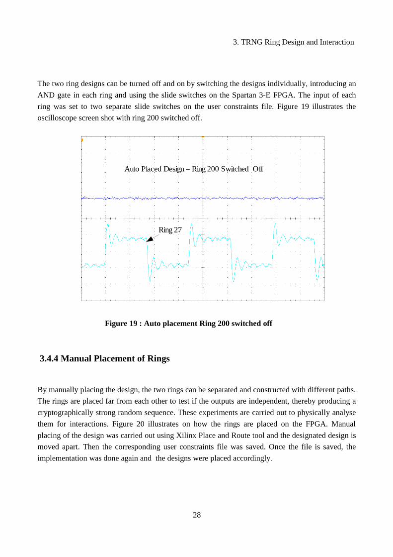
The two ring designs can be turned off and on by switching the designs individually, introducing an
AND gate in each ring and using the slide switches on the Spartan 3-E FPGA. The input of each
ring was set to two separate slide switches on the user constraints file. Figure 19 illustrates the
oscilloscope screen shot with ring 200 switched off.
Figure 19 : Auto placement Ring 200 switched off
3.4.4 Manual Placement of Rings
By manually placing the design, the two rings can be separated and constructed with different paths.
The rings are placed far from each other to test if the outputs are independent, thereby producing a
cryptographically strong random sequence. These experiments are carried out to physically analyse
them for interactions. Figure 20 illustrates on how the rings are placed on the FPGA. Manual
placing of the design was carried out using Xilinx Place and Route tool and the designated design is
moved apart. Then the corresponding user constraints file was saved. Once the file is saved, the
implementation was done again and the designs were placed accordingly.
28
Auto Placed Design – Ring 200 Switched Off
Ring 27

3. TRNG Ring Design and Interaction
Figure 20 : Manual placement
The two ring designs can be turned off and on by switching the designs by introducing an AND gate
and using the slide switches similar to the auto placement design. Figure 22 illustrates the
oscilloscope screen shot with ring 200 switched off.
Observing the two output signals from the experimented designs, the output from the Ring 200
above and Ring 27 below from the oscilloscope, the interactions are interpreted. Figure 19 and 22
shows the oscilloscope screen shots for the auto and manual placement respectively. By visually
observing the signal outputs, the two designs does not seem to be much different. However, the
designs should be subjected to data analysis for further investigation of the ring interactions. The
data from the observed output has to be saved and later analysed.
29
200 Rings40 Rings each
(7,11,13,17,19)Inv's
One Ring 27 Inv's
Xilinx Spartan 3 - E
Logic Utilized(Filled)
FPGAFloor

3. TRNG Ring Design and Interaction
Figure 21 : Manual placement output
Figure 22 : Manual placement Ring 200 turned off
30
Ring 200
Ring 27
Manually Placed Design – Ring 200 Switched Off
Ring 27
3. TRNG Ring Design and Interaction
3.5 Data Analysis - Correlation
The data analysis of the recorded signal outputs from the oscillators was performed in MATLAB.
Several sets of the recorded outputs from the Ring 200 and Ring 27 designs saved by the
oscilloscope was copied to the PC and analysed using MATLAB.
CorrelationCorrelation is a property which determines the degree of similarity between two signals. It is rather
the statistical relationship between two or more random variables. Such kind of relationships are
studied for several applications to define the correlation property amongst them [16].
Cross CorrelationThe correlation of two signals by applying the function of time lag to one of them is known as cross
correlation. It is a function that measures the dependence of values of one signal to the other.
Correlation between two discrete time signals are given below,
consider x(n) and v(n)
( 3 )
or
( 4 )
From the equations above, the correlation is the sum of the product of one signal to other shifted.
Say if the two signals are interchanged, then
( 5 )
Hence, Rxv(m) = Rvx(-m) meaning one correlation is the flipped version of the other. 'M' denoted in
all the three equations refers to the length of the data samples. M = 850 in all the correlation
analysis carried out as show in figure 23 and 24.
31
Rxv m= ∑n=−M
M
x nv n−mwhere m=0,±1,±2,. .....
Rxv m= ∑n=−M
M
x nmv nwhere m=0,±1,±2, ......
Rvx m= ∑n=−M
M
v nx n−m where m=0,±1,±2,......
3. TRNG Ring Design and Interaction
Autocorrelation Auto correlation is the function of a random signal which derives the dependence of samples at one
time period to the values of samples of another time period. It is the cross correlation of a signal to
itself. The auto correlation of a signal x(n) is given below,
( 6 )
or
( 7 )
The autocorrelation is maximum when m=0, the signal is then superimposed within itself. The
autocorrelation property decreases when the value of m increases in both directions. Thus we can
derive it as an even symmetric function, Rxx (m) = Rxx(-m). 'M' denoted in the equations refers to
the length of the data samples. M = 850 in auto-correlation analysis carried out as show in figure 24.
Cross Correlation of Ring 200 Vs. Ring 27
The cross correlation of the two signals from Ring 200 and Ring 27 was performed. The data
samples were collected from the oscilloscope by saving the data points of the signal at a particular
time instant. Using the single shot option which is available on tektronix oscilloscopes, the signal
was saved for every signal high from Ring 27. This looks like a square wave form and its
corresponding signal part of the Ring 200 was saved. Similarly, every signal low and its
corresponding Ring 200 signal part was saved. Finally they were copied together and saved as two
sets of datas for Auto and Manual place and route designs. Please refer appendix 2 for detailed
screen shots on measuring the signal outputs by fixing the cursors on the oscilloscope. The steps
followed while deriving the correlation was,
• Normalize the signal ring 200 and ring 27 separately to make the crossing at zero amplitude.
• Generate a math rand signal with the length of ring 200. 'Rand' is a function from MATLAB
that generates uniformly distributed random numbers.
• Normalize the newly generated math rand signal with the sum of the signal and ring 27.
• Finally cross correlate the signals ring 200 vs. ring 27 and math rand generated signal. The
MATLAB function Xcorr was used for correlation from the signal processing tool box.
32
Rxx m=∑n=−∞
∞
x n x n−m
Rxx m=∑n=−∞
∞
x nmx n

3. TRNG Ring Design and Interaction
Figure 23 illustrates the cross correlation of the auto and manual designs for peak signal values. The
blue waveform accounts for the manual place and routed design, while the red waveform accounts
for auto place and route design. The inner green and black waveforms accounts for ring 27 vs. math
rand for manual and auto designs respectively.
Figure 23 : Cross correlation - auto and manual P&R signal high
Figure 24 : Cross correlation - auto and manual P&R signal low
33
0 100 200 300 400 500 600 700 800 900-150
-100
-50
0
50
100
150
length
data
Correlation LOW - Auto & Manual P&R
0 100 200 300 400 500 600 700 800 900-150
-100
-50
0
50
100
150
length
data
Correlation PEAK - Auto & Manual P&R
3. TRNG Ring Design and Interaction
The idea behind separating the two rings, placing them far from each other, was to observe the
effects of the level of interaction between them. Thus from the above MATLAB plots, we can
observe that the manual placed design, the blue waveform, is higher than that of the auto placed red
waveform. Thus from the above experiments, we observe that there are strong interactions between
the rings and while separating them there are not much difference in their independence. Thus, even
though they are separated, the independence between the signal outputs does not seem to improve.
Autocorrelation of Ring 200
The autocorrelation is the correlation a signal with itself. Ring 200 was autocorrelated, by extracting
the data points of the signal from the oscilloscope as described above in cross correlation. The
MATLAB function Xcorr was used to autocorrelate the signal from ring 200. Math rand, the
random function from MATLAB, was generated with the length of ring 200 and autocorrelated. The
autocorrelation of two signals were later plotted together.
Figure 25 : Autocorrelation - Ring 200
34
0 100 200 300 400 500 600 700 800 900-400
-200
0
200
400
600
800
1000
1200
1400
length
data
Auto-Correlation - Ring 200
3. TRNG Ring Design and Interaction
Figure 25 shows the plot of auto correlation of the ring 200 shown by colour magenta and the green
waveform account for the math rand signal along with the length of ring 200.
Cross Correlation - Two Separate FPGA Boards
In order to test the design further, the ring 200 was implemented on two separate Spartan FPGA
boards. Then the data points were recorded and finally cross correlated in MATLAB. It was
performed in order to show separate designs from different interface boards and recording them in
an oscilloscope at the same time. Same configuration file was ported to two separate evaluation
boards with similar Spartan 3 E model FPGAs.
Figure 26 : Cross correlation Ring 200 from different evaluation boards.
Figure 26 shows the cross correlation of two separate designs which by no means can have
interacted with each other.
35
0 200 400 600 800 1000 1200 1400 1600 1800 2000-500
-400
-300
-200
-100
0
100
200
300
400
500
length
data
Correlation Two 200 Rings Two Boards

36

4. Jitter Analysis
4. Jitter Analysis
4.1 Jitter Classification
Jitter from electronic devices, meaning the short variations relative to the ideal positions of a digital
signal forms the source of randomness [17]. Although jitter is an undesired factor for many
applications, for a random number generator, having more jitter serves the purpose of randomness.
Figure 27 presents a classification of types of jitter [17].
Figure 27 : Jitter classification
Figure 28 illustrates a jittering trace model where the dotted lines indicate the ideal edges of a
measured signal. Both the rising time and falling time edges of a signal are affected by the jitter.
Usually, jitter is classified as deterministic jitter and non-deterministic jitter. Deterministic jitter is
further subdivided into the types periodic jitter, duty cycle jitter and data-dependent jitter [17]. Non-
deterministic jitter is responsible for true random number generation, and is also known as random
jitter. Deterministic jitter is caused by cross talk and switching between the interface signals and
outputs. The spikes from the current caused by switching the output pins also causes jitter. Random
jitter on the other hand is derived from the crystal oscillations, thermal vibrations and several such
kinds of sources. It is a timing noise which is not predictable due to its pattern. A normal Gaussian
distribution is set as a model for the random jitter. The duty cycle type of jitter is used in our
analysis.
37
Jitter distribution(Total Jitter)
Random Jitter
Deterministic Jitter
Periodic Jitter
Data dependent Jitter
Duty Cycle Jitter

4. Jitter Analysis
4.2 Phase Metrics
An example of the phase difference between the measured output and the advance of the clock fromthe ideal clock is shown in Figure 28. Jitter is the deviation of the timing edges from the ideallocations. Duty cycle jitter is the deviation from the ideal value of the duty cycle.
Figure 28 : Clock jitter model
4.3 Jitter Measurements
There are several types of test equipment using different approaches to measure jitter [21]. These
are oscilloscopes, spectrum analysers, automatic test equipment and special jitter measurement
devices. In our analysis an oscilloscope was used to measure the signal and the recorded signal data
was transferred to the PC to analyse the jitter using MATLAB.
4.4 Jitter in Ring Oscillators
Jitter in Ring oscillators, which is the noise source for the TRNG, can be further analysed. For this
purpose the raw oscillating signal from the oscillator was recorded on the Tektronix DPO4104
oscilloscope. For the experimental purpose a ring oscillator with 51 inverters producing a frequency
of 27 MHz was designed and its output was measured. Two rings with 51 inverters were placed
close to each other manually on the FPGA and the outputs were recorded. Similarly next, only one
ring with 51 inverters was placed in the same place, constrained to a particular area on the FPGA.
The outputs were driven through the I/O pins and Tek 1.5 Ghz active probes were used to measure
the signals. The data points recorded were taken as two sets of 50,000 samples at 5 GSamples/sec.
Figure 29 shows how the rings were placed on the FPGA. To analyse the jitter the signal data was
recorded and sent to the PC and the duty cycle jitter was extracted, then the analysis was carried out
to detect dependency between the rings. The physical interactions contribute to several factors that
are involved in the FPGA on a hardware level such as electromagnetic interactions, crosstalk,
ground bounce etc., which form the non-linear effects on jitter [18].
38
Ideal edges Measured Output
T1 T2
C0 C1 C2

4. Jitter Analysis
Figure 29 : Ring 51 placement
The samples recorded from the oscilloscope would oscillate between VDD and GND, and so the
signal was normalized to make the crossing occurring at zero amplitude. The exact locations of
ideal edges were determined. For each of the rising edge, the time displacement with respect to the
ideal edge location is the jitter value. This jitter model is defined by the incremental jitter in [18] as
shown in Figure 28.
4.4.1 Incremental Jitter Accumulation Model
The incremental jitter or momentary jitter accumulation was calculated from the recorded data
signal by extracting the duty cycle jitter of the ring oscillator signal. The incremental jitter
calculation was performed in accordance with reference [18].
The incremental jitter accumulation model as shown in Figure 27 is defined by
( 8 )
Incremental jitter accumulation here is described as a linear jitter accumulation.
The distribution of the incremental jitter is modelled as a random variable Xi.
T is the average period. 'i' denotes for Ti = T1,T2,T3,........ the time durations as shown in Figure 27,
where each element is representative of the period of the 'i'th clock cycle [18].
39
Close Rings Single Ring
Xilinx Spartan 3-E FPGAFloor
Xilinx Spartan 3-E FPGAFloor
Ring 51Ring 51
.....I = 1 I = 51
Ring Oscillator 51 Inverters
X i=T i−T

4. Jitter Analysis
Once the recorded data was ported to MATLAB, the momentary period of the signal has to be
calculated. The ideal rise time was calculated between two values when the signal rises from a
negative to a positive value. This is done by linear approximation of the preceding and following
values. When the ideal edges are found, the momentary period can be calculated, as 'C0-C1,...'. The
difference on ideal edges is the period for each clock cycle,'T1,...'. The average of T is calculated as
'Ti'. Finally, the incremental jitter is calculated from the difference between individual periods and
the average period.
( 9 )
In general ( 10 )
( 11 )
In general ( 12 )
Thus the incremental jitter was derived and the values were plotted in MATLAB. However these
outputs are measured before the post processing and they are raw signal outputs from the
oscillators. Observing the signals, the jitter plot can be seen as a periodic pattern in figure 30 and
31.
Figure 30 : Incremental jitter accumulation plot for a 51 inverter ring, two rings together
40
T 1=C0−C1 ,T 2=C1−C2 , T 3=C 2−C3 ......
X 1=T 1−T , X 2=T 2−T , X 3=T 3−T .......
X i=T i−T
T i=C i1−C i
0 50 100 150 200 250
-2
-1
0
1
2
3x 10
-11 PERIOD Jitter - Two Rings
length(time)
Incre
menta
l jit
ter,
Xi in
seconds

4. Jitter Analysis
Figure 31 : Incremental jitter accumulation plot for a 51 inverter ring, single ring
The incremental jitter plots from Figures 30 and 31 show the outputs when the two rings are placed
on the FPGA close to each other and when only one ring was placed respectively. The two figures
show relatively similar periodic patterns. The periodic nature from both the designs, as illustrated in
figure 30 and 31, are due to the phase interlock between the inverters of each ring oscillator. This is
compared later in Chapter 6 when the same incremental jitter is calculated for astable oscillators.
Chapter 6 discuss the development of a separate piece of hardware with astable oscillators and the
calculation of incremental jitter for these oscillators.
41
0 50 100 150 200 250
-2
-1
0
1
2
3x 10
-11 PERIOD Jitter - Separate
length(time)
Incre
menta
l jit
ter,
Xi in
seconds

42

5. Sampling Techniques and Interface
5. Sampling Techniques and Interface
Until now the noise source and the development of ring oscillators has been discussed in Chapter 2
and Chapter 3. Once the noise source was developed, the output from the XOR of several oscillators
has to be sampled. The goal of the TRNG is to harvest the entropy source by sampling. The
deterministic part is not changed, while sampling the uncertain transition zones. The sampling
extracts the random jitter from the ring oscillators [19].
5.1 Sampling
The sampling is usually done by several approaches. The XORed output can be sampled by using
the output of another ring oscillator, for example a coupled oscillator. Or the signals of few ring
oscillators are combined. Using a D type flip flop corresponds to one such form of implementation.
Sampling of the signals have to be carried out from lower or similar frequencies. This can cause
more metastability effects in the D flip flop which reduces the mutual coupling effects. The ring
lengths for several ring oscillators were chosen in the range of relatively prime [4].
Figure 32 : Sampled design
The ring oscillator output once XORed is sampled using the D flipflop as shown in figure 32. The
output from sampled output is now called a 'DAS' signal as discussed in the introduction part of the
TRNG. The output later has to be subjected to post processing.
43
....
....
....
....
....
D-type FlipFlop
Clock freq,fs
I = 1 I = 7
I = 1
I = 1
I = 1
I = 1
I = 11
I = 13
I = 17
I = 19
Output200 Rings
......
......
K = 200
K = 1
5. Sampling Techniques and Interface
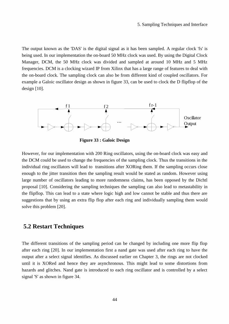
The output known as the 'DAS' is the digital signal as it has been sampled. A regular clock 'fs' is
being used. In our implementation the on-board 50 MHz clock was used. By using the Digital Clock
Manager, DCM, the 50 MHz clock was divided and sampled at around 10 MHz and 5 MHz
frequencies. DCM is a clocking wizard IP from Xilinx that has a large range of features to deal with
the on-board clock. The sampling clock can also be from different kind of coupled oscillators. For
example a Galoic oscillator design as shown in figure 33, can be used to clock the D flipflop of the
design [10].
Figure 33 : Galoic Design
However, for our implementation with 200 Ring oscillators, using the on-board clock was easy and
the DCM could be used to change the frequencies of the sampling clock. Thus the transitions in the
individual ring oscillators will lead to transitions after XORing them. If the sampling occurs close
enough to the jitter transition then the sampling result would be stated as random. However using
large number of oscillators leading to more randomness claims, has been opposed by the Dichtl
proposal [10]. Considering the sampling techniques the sampling can also lead to metastability in
the flipflop. This can lead to a state where logic high and low cannot be stable and thus there are
suggestions that by using an extra flip flop after each ring and individually sampling them would
solve this problem [20].
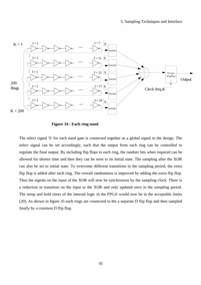
5.2 Restart Techniques
The different transitions of the sampling period can be changed by including one more flip flop
after each ring [20]. In our implementation first a nand gate was used after each ring to have the
output after a select signal identifies. As discussed earlier on Chapter 3, the rings are not clocked
until it is XORed and hence they are asynchronous. This might lead to some distortions from
hazards and glitches. Nand gate is introduced to each ring oscillator and is controlled by a select
signal 'S' as shown in figure 34.
44
...
f 1 f 2 f r-1
Oscillator Output
5. Sampling Techniques and Interface
Figure 34 : Each ring nand
The select signal 'S' for each nand gate is connected together as a global signal in the design. The
select signal can be set accordingly, such that the output from each ring can be controlled to
regulate the final output. By including flip flops to each ring, the random bits when required can be
allowed for shorter time and then they can be reset to its initial state. The sampling after the XOR
can also be set to initial state. To overcome different transitions in the sampling period, the extra
flip flop is added after each ring. The overall randomness is improved by adding the extra flip flop.
Thus the signals on the input of the XOR will now be synchronous by the sampling clock. There is
a reduction in transition on the input to the XOR and only updated once in the sampling period.
The setup and hold times of the internal logic in the FPGA would now be in the acceptable limits
[20]. As shown in figure 35 each rings are connected to the a separate D flip flop and then sampled
finally by a common D flip flop.
45
....
....
....
....
....
D-type FlipFlop
Clock freq,fs
I = 1 I = 7
I = 1
I = 1
I = 1
I = 1
I = 11
I = 13
I = 17
I = 19
Output200 Rings
......
...
...
K = 200
K = 1
NAND
S
NAND
NAND
S
NAND
S
NAND
NAND
S
NAND
S

5. Sampling Techniques and Interface
Figure 35 : Each ring D-FF
The 'fsi' is the same sampling frequency for all the DFF of each rings as seen from the figure 35.
The ring oscillator outputs are connected to each separate flip flops before the whole outputs are
sampled again.
5.3 Post Processing
The next step on the design of the TRNG is post-processing the sequence from the sampled output.
Post-processing improves the statistical homogeneity of the generator. The compressing function is
applied to the sequence. The entropy is distilled from the sequence resulting in increase of the
randomness [5]. The sequence is uniformly distributed. There are several types of post-processing
algorithms available such as XOR correction, Von Neumann correction, extractor function, hash
function and resilient functions [22]. In our implementation Von Neumann corrector have been
used. Many imperfections of the entropy source is being corrected by processing them by any such
kind of correction schemes. The bits from the raw data of the entropy source includes abnormalities
and bias would not exist any more once post-processed .
The evaluation of a random number generator is performed by the statistical tests such NIST and
BSI. When an improvement is required on the statistical properties of the random bit sequence, the
post-processing is performed before they are subjected for such statistical tests.
46
....
....
....
....
....
D-type FlipFlop
Clock freq,fs
I = 1 I = 7
I = 1
I = 1
I = 1
I = 1
I = 11
I = 13
I = 17
I = 19
Output200 Rings
......
......
K = 200
K = 1D
Flipflop
D Flipflop
D Flipflop
D Flipflop
D Flipflop
fsi
fsi
fsi
fsi
fsi
fsi
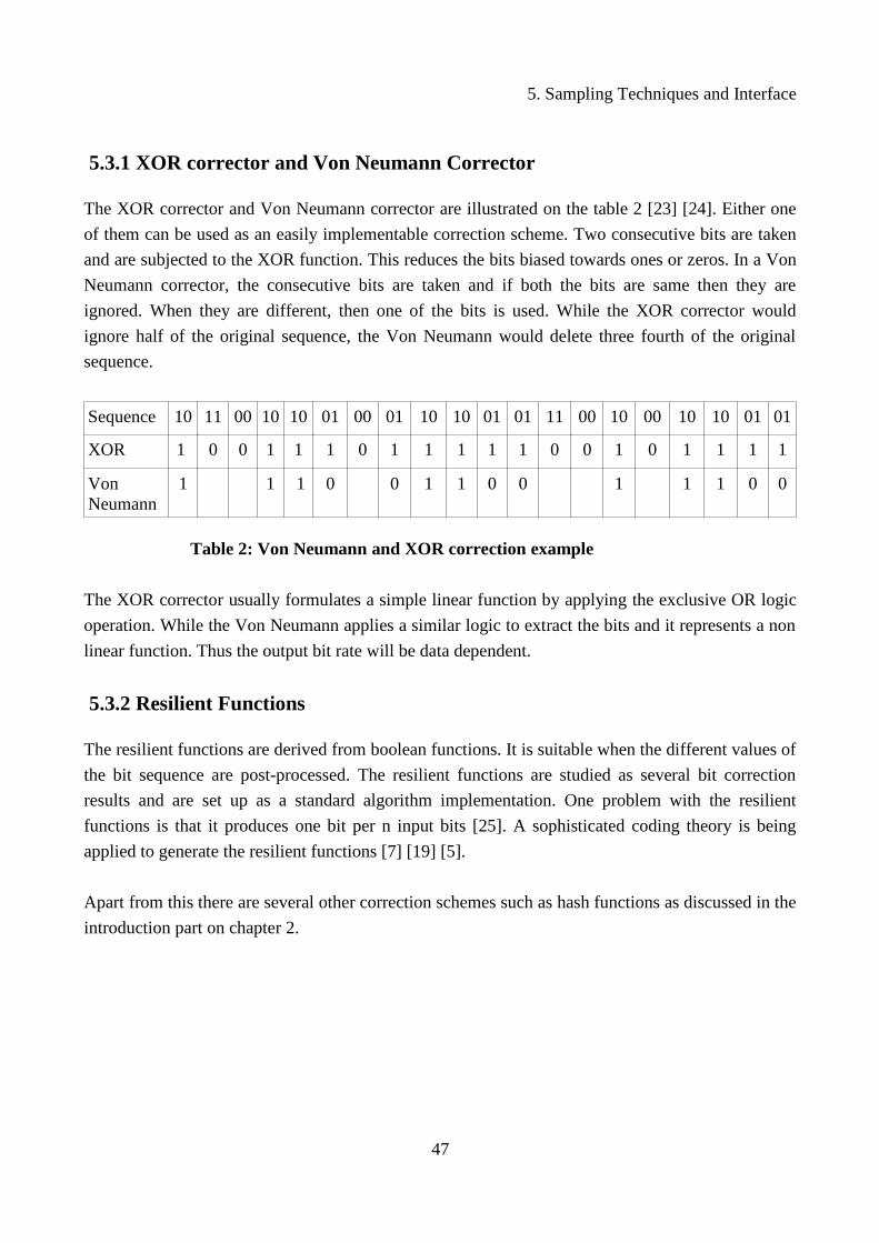
5. Sampling Techniques and Interface
5.3.1 XOR corrector and Von Neumann Corrector
The XOR corrector and Von Neumann corrector are illustrated on the table 2 [23] [24]. Either one
of them can be used as an easily implementable correction scheme. Two consecutive bits are taken
and are subjected to the XOR function. This reduces the bits biased towards ones or zeros. In a Von
Neumann corrector, the consecutive bits are taken and if both the bits are same then they are
ignored. When they are different, then one of the bits is used. While the XOR corrector would
ignore half of the original sequence, the Von Neumann would delete three fourth of the original
sequence.
Sequence 10 11 00 10 10 01 00 01 10 10 01 01 11 00 10 00 10 10 01 01
XOR 1 0 0 1 1 1 0 1 1 1 1 1 0 0 1 0 1 1 1 1
VonNeumann
1 1 1 0 0 1 1 0 0 1 1 1 0 0
Table 2: Von Neumann and XOR correction example
The XOR corrector usually formulates a simple linear function by applying the exclusive OR logic
operation. While the Von Neumann applies a similar logic to extract the bits and it represents a non
linear function. Thus the output bit rate will be data dependent.
5.3.2 Resilient Functions
The resilient functions are derived from boolean functions. It is suitable when the different values of
the bit sequence are post-processed. The resilient functions are studied as several bit correction
results and are set up as a standard algorithm implementation. One problem with the resilient
functions is that it produces one bit per n input bits [25]. A sophisticated coding theory is being
applied to generate the resilient functions [7] [19] [5].
Apart from this there are several other correction schemes such as hash functions as discussed in the
introduction part on chapter 2.
47

5. Sampling Techniques and Interface
5.4 Interface
The interface circuitry required to transmit the bit sequence from the FPGA board to the PC was
carried out through the RS 232 port of the Spartan 3-E evaluation board. Figure 36 illustrates the
block level view of how the bits are generated from the ring oscillators, then corrected by the digital
post processing, and finally transmitted by the interface block to the PC via the RS 232 serial port.
Figure 36 : Block outline, interface
The interface block was implemented by a FIFO-UART (Universal Asynchronous Receive
Transmit) combination and transmitted via the serial port. The signal from the von neumann
correction would be shifted to decrease to an 8 bit vector. The FIFO, UART combination used in
this system has a width of 8 bits. The sequence after sampling and digital correction is measured as
an 8 bit width signal, collected in a FIFO. The FIFO-copy block was used as a control block, the
data is sent to the UART block without loss of any bits. There are enough functionalities to check
the FIFO block with fill and empty signals respectively. The FIFO copy forms the intermediate
block between the UART and the fifo block. Once the FIFO copy receives the data, the UART
transmit is synced with the data signal and the 8 bit signal is received at the UART data-in. The
UART then communicates with a fixed baud rate to transmit and receive data from the PC.
However, only the transmit block was used in this implementation as the generated sequence was
transmitted to the PC.
Figure 37 : Interface block
48
Noise Source200 RO Xored,
Sampled
Von Neumann Corrector
Interface Block&
RS-232 SerialTo PC
Serial Tx.Signal
Control Signals
Shift Register
Sampled, Corrected Signal
FifoBlock
FIFO
Copy
UARTBlock
8
8

5. Sampling Techniques and Interface
TeraTerm, a serial port connection communication program was used to receive the bits on the PC
and stored as a bit file.
FIFO Block
An 8 bit FIFO is shown in figure 38. The write data is the 8 bit data signal which is fed as the input
data to the FIFO. There is an internal reset for the whole interface block. The data is written to the
FIFO on the rising edge of the clock. The write and read enable signals controls the data writing
procedures. The flag of the empty signal is set high and is connected to the FIFO copy block.
Figure 38 : FIFO block
FIFO Copy Block
The FIFO copy is an intermediate block between the FIFO and the UART. The read enable signal is
connected to the FIFO block to control the data signal. The full control signal from FIFO copy is
connected to the Txd_Busy signal of the transmitter section of the UART, while the write enable
signal connects the sending request to the transmitter of the UART.
Figure 39 : FIFO copy
49
FIFOBlock
8Write_data
Clk
Rst_n
w_enabler_enable
R_data8
empty
FifoCopy
empty r_en
w_enablefull
Clk
Rst_n
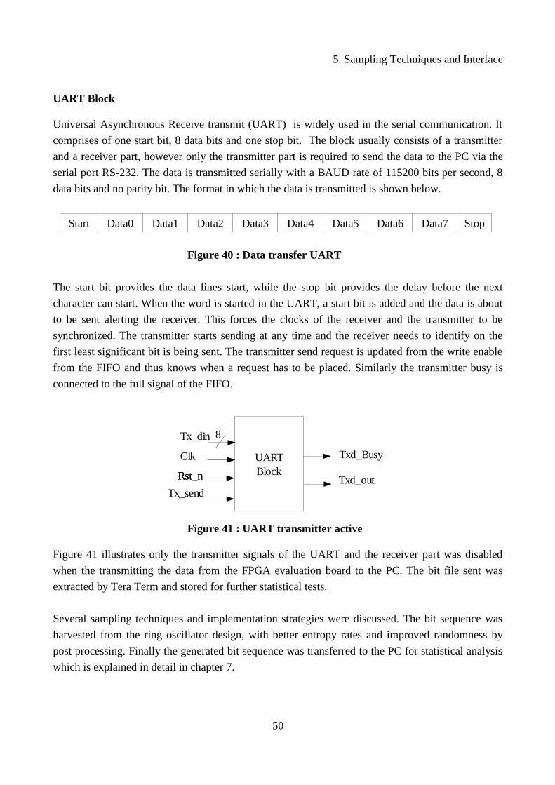
5. Sampling Techniques and Interface
UART Block
Universal Asynchronous Receive transmit (UART) is widely used in the serial communication. It
comprises of one start bit, 8 data bits and one stop bit. The block usually consists of a transmitter
and a receiver part, however only the transmitter part is required to send the data to the PC via the
serial port RS-232. The data is transmitted serially with a BAUD rate of 115200 bits per second, 8
data bits and no parity bit. The format in which the data is transmitted is shown below.
Start Data0 Data1 Data2 Data3 Data4 Data5 Data6 Data7 Stop
Figure 40 : Data transfer UART
The start bit provides the data lines start, while the stop bit provides the delay before the next
character can start. When the word is started in the UART, a start bit is added and the data is about
to be sent alerting the receiver. This forces the clocks of the receiver and the transmitter to be
synchronized. The transmitter starts sending at any time and the receiver needs to identify on the
first least significant bit is being sent. The transmitter send request is updated from the write enable
from the FIFO and thus knows when a request has to be placed. Similarly the transmitter busy is
connected to the full signal of the FIFO.
Figure 41 : UART transmitter active
Figure 41 illustrates only the transmitter signals of the UART and the receiver part was disabled
when the transmitting the data from the FPGA evaluation board to the PC. The bit file sent was
extracted by Tera Term and stored for further statistical tests.
Several sampling techniques and implementation strategies were discussed. The bit sequence was
harvested from the ring oscillator design, with better entropy rates and improved randomness by
post processing. Finally the generated bit sequence was transferred to the PC for statistical analysis
which is explained in detail in chapter 7.
50
Clk
Rst_n
UARTBlock
Tx_din 8
Rst_n
Tx_send
Txd_Busy
Txd_out

6.Oscillator Board Design
6.Oscillator Board Design
A new set of oscillators apart from the ring oscillator as a noise source was developed. The
oscillators would be developed on a separate PCB and then attached to the FPGA evaluation board
externally as a new noise source. Astable oscillators, consisting of a simple circuitry that would
oscillate in a frequency of a few hundred KHz was chosen. The oscillators would operate at
different frequencies and 10 oscillators each oscillating in individual frequencies was designed. The
idea of developing the different oscillators as a separate source was the possibility to have lesser
influence or interactions from each other when compared to that of the ring oscillators inside the
FPGA. After the whole PCB design was developed, the electronic components were placed on the
PCB and finally connected to the FPGA through the I/O pins. Finally, the oscillating signals were
XORed and sampled inside the FPGA and subjected to the statistical tests for evaluation.
A detailed analysis of the jitter from the oscillators similar to that of the ring oscillators were
performed. The jitter comparison from the ring oscillators implemented in the FPGA could be
analysed and checked for variations compared to independent oscillators. In the astable oscillators
the period of the oscillations were constrained towards prime number lengths.
In practice there are several oscillators used such as crystal oscillator, voltage controlled oscillator,
opto electronic oscillators, RLC oscillator etc. The oscillators are in general divided into harmonic
oscillators and relaxation oscillators. The harmonic oscillators produces the sinusoidal output while
the relaxation oscillator produces a non-sinusoidal waveform like square wave. Both the ring
oscillators and the astable oscillators are a form of relaxation oscillator. The astable oscillators are
two state circuits that are quite simple in design. The design of the transistor based multivibrator
would effect the jitter from the period which shall form as the source of randomness in the design. It
was used for experimental purpose and analysis.
A step by step procedure towards a hardware development was carried out. An oscillator design was
developed followed by simulations for different values considering the component tolerances using
LT SPICE from Linear Technology.
51
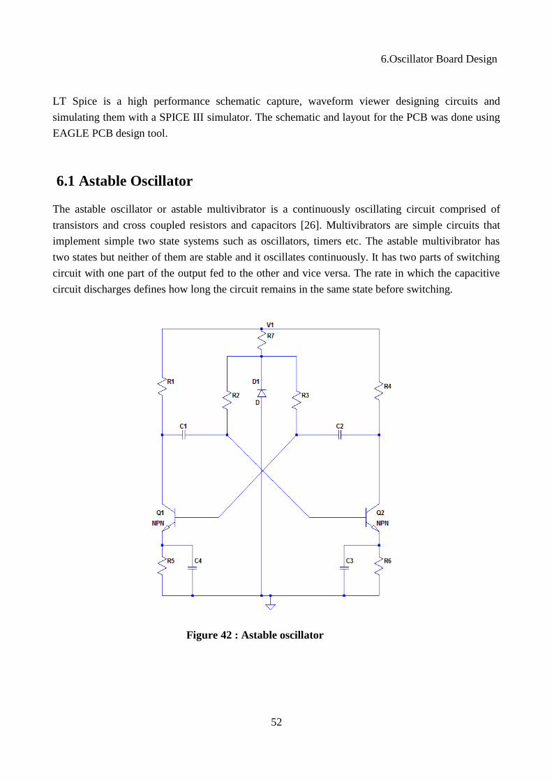
6.Oscillator Board Design
LT Spice is a high performance schematic capture, waveform viewer designing circuits and
simulating them with a SPICE III simulator. The schematic and layout for the PCB was done using
EAGLE PCB design tool.
6.1 Astable Oscillator
The astable oscillator or astable multivibrator is a continuously oscillating circuit comprised of
transistors and cross coupled resistors and capacitors [26]. Multivibrators are simple circuits that
implement simple two state systems such as oscillators, timers etc. The astable multivibrator has
two states but neither of them are stable and it oscillates continuously. It has two parts of switching
circuit with one part of the output fed to the other and vice versa. The rate in which the capacitive
circuit discharges defines how long the circuit remains in the same state before switching.
Figure 42 : Astable oscillator
52

6.Oscillator Board Design
Figure 42 shows a simple astable oscillator design with identical sets of components on each side
that oscillates and the output is driven from the collector or emitter terminal of the transistor.
The first state is when Q1 is switched on allowing a base current to flow. Thus, its is in the
saturation mode allowing the current to flow through the collector. At this instant the collector
voltage of Q1 is low and also the capacitor C1 is discharged. The transistor Q2 is off as the base
voltage would be low and not enough to start switching. When Q1 charges the capacitor C1, the
base voltage of Q2 increases until it is enough to switch on Q2. At this instant, the current flows
through the collector and that drops the collector voltage. Since the capacitor C2 voltage is not
completely changed, the base voltage of Q1 will decrease so that the transistor Q1 will be switched
off. Similarly, the second half cycle is generated when the current flows through Q2 and continues
until Q1 is turned on. Thus the whole cycle is generated and it continues to oscillate in this manner
[27].
The two capacitor C4 and C3 are mostly used as a RC combination along with the two resistors
connected to the emitter of the two transistors. These capacitors would contribute to extend the rise
time of the oscillator output though the emitter terminals of the transistors.
Q2's collector potential tends to the voltage V1 as C2 charges rapidly with time constant of
( 13 )
A simple equation to derive the approximate value of the period of the multi-vibrator is given by
( 14 )
While the frequency of the oscillator is given by, where the clock cycle is proportional to the
expression (R2*C1+R3*C2).
( 15 )
The resistor R7 is used in connecting with the breakdown voltage of the zener diode D1 as a
protecting element and sets the desired generating voltage levels. It protects the circuit from the
reverse breakdown when the supply voltage goes high.
53
T 2=R3∗C2
T=R2∗C1R3∗C2
f =1/T =1/R2∗C1R3∗C2

6.Oscillator Board Design
6.2 Circuit Design
The astable oscillator was designed for several frequencies. The frequencies are achieved by the RC
combination of R2 C1 and R3 C2.
Figure 43 : Astable oscillator approx. freq = 66 KHz
Figure 43 shows the astable oscillator that has been designed to oscillate at 66 KHz. The operating
voltage for the circuit is 10 V. It is evident that the components of the left side are a mirror of the
right side. The zener diode used here has a 4.7 V breakdown voltage to protect and drive the circuit.
54
Output Output

6.Oscillator Board Design
To simulate the oscillator, a transient analysis was run. The simulator takes small time steps
simulating the circuit state at each step. Figure 44 illustrates the simulation output of the above
constructed oscillator. It was measured at the emitter terminal of the transistor and operates at
around 66 KHz frequency.
Figure 44 : Simulation output (LT spice)
Another important factor that has to be taken care of while designing the oscillators is the operating
emitter voltage as shown in the figure 44, which should be between "2.2 V to 3 V". This is the
voltage level for a logic 1 with a maximum of 3V and logic 0 with a minimum of 2 V for the FPGA
I/O pins. Hence care was taken to design the circuit in the desired voltage levels by repeated
simulations.
6.2.1 Different Oscillating Frequencies
The same procedure was followed to design 10 oscillators operating at different frequencies. The
components required for the design was chosen and the tolerance levels had to be as small as
possible so that the final output from the board would be close to the simulations. The simulations
were carried out for all the oscillators including the tolerance percentages. The resistors, capacitors,
zener diode and the operating voltages of the transistors were all taken into consideration while they
were simulated. The oscillating frequencies were chosen as relative prime widths. Initially there was
difficulties in running the oscillators at the exact frequencies compared to simulation and real time
operation after the components were placed on the PCB.
The different frequencies achieved with 10 oscillators are : 92 Khz, 156 Khz, 94 Khz, 195 Khz,
83Khz, 84 Khz, 73 Khz, 160 Khz, 66 Khz, 65 Khz.
55
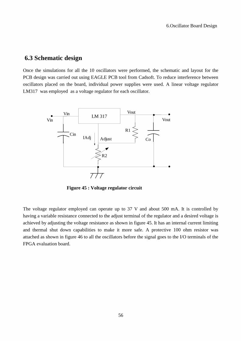
6.Oscillator Board Design
6.3 Schematic design
Once the simulations for all the 10 oscillators were performed, the schematic and layout for the
PCB design was carried out using EAGLE PCB tool from Cadsoft. To reduce interference between
oscillators placed on the board, individual power supplies were used. A linear voltage regulator
LM317 was employed as a voltage regulator for each oscillator.
Figure 45 : Voltage regulator circuit
The voltage regulator employed can operate up to 37 V and about 500 mA. It is controlled by
having a variable resistance connected to the adjust terminal of the regulator and a desired voltage is
achieved by adjusting the voltage resistance as shown in figure 45. It has an internal current limiting
and thermal shut down capabilities to make it more safe. A protective 100 ohm resistor was
attached as shown in figure 46 to all the oscillators before the signal goes to the I/O terminals of the
FPGA evaluation board.
56
..
LM 317
..
CinAdjustIAdj
R2
R1
Co
Vout
.
Vin
Vin Vout .

6.Oscillator Board Design
Figure 46: Image eagle schematic entry
Figure 46 shows a part of the Eagle schematic entry of the circuit. Please refer to the appendix for
the whole schematic of the board designed. A half Euro card size of (100 x 80) mm was used for the
design. Two such boards were implemented with five oscillators in one board and the remaining
five oscillators on the second board. A majority of components used were SMD type voltage
regulators, resistors and capacitors with package types 0805 and 0603. The transistors, diodes and
the variable resistor are through hole components. Hence, the components can be placed within the
provided dimension space of the PCB. To measure, make connections to the evaluation board and
power supply, several pins were used. After the entire schematic entry was finished, the Electrical
Rule Check (ERC) was run to check different constraints regarding the connections.
6.4 PCB Layout
The PCB layout from the entered schematic entry was created. A top and bottom layer design was
made and separate rails for the VCC connection were used. The ground polygon was drawn on the
entire board on both the top and bottom layers and was placed with vias at the necessary regions
where the ground connections are needed. This helps in proper ground for the components and the
board.
57

6.Oscillator Board Design
Figure 47 : Image eagle layout
Figure 47 shows an image from the eagle layout editor where an oscillator components placed and
the connections are drawn.
The design was sent for manufacturing of the PCB boards, and soldering of the components were
performed. Two identical boards were manufactured as the component foot prints for both the
boards would be similar and only the component values will differ from the two boards. Please refer
the picture of the PCB boards in the appendix.
The boards were powered up and the transistors started to oscillate after gradually increasing the
voltage levels. The frequency achieved from the circuit are pretty low and such kind of oscillators
operates in the range of few hundred kilo hertz. Even though the desired frequency can be achieved
while simulating the circuit, in real time it was quite different. When the board was powered up it
was observed that the capacitances used in the range of few pico farads used initially were
responsible for the oscillators from not working. These low capacitances could be same or smaller
than the PCB tracks which would be one of the reasons. When increasing the capacitance values,
the oscillators seem to work fine, but at the cost of the frequency. Hence, about few hundred kilo
hertz is the range that could be achieved from such a circuit in practice. It is employed for
experimental purpose only and a range of frequencies as described in section 6.2.1 was achieved.
58

6.Oscillator Board Design
6.5 Correlation and Jitter Analysis
The output from oscillators were measured on the oscilloscope and the correlation and jitter analysis
for the oscillators was carried out. This is similar to the schemes that was used for the ring
oscillators implemented on the FPGA as described in chapter 3.
Figure 48 : An oscillator output from the new oscillator board
The data from the oscillators were recorded from the oscilloscope and was later saved to the PC for
analysis. Figure 48 shows the oscillator output from a 73 KHz oscillator.
To cross correlate and run the jitter analysis, two sets of 5000 points sampled at over 250 MS/s
were recorded. For cross correlation the signal is first normalized for a zero average. Then it is cross
correlated with the math rand random generation function from MATLAB. The length of the math
rand function is extended to that of the length of the oscillator signal and sum before it is cross
correlated by the MATLAB function Xcorr. Figure 49 shows the cross correlation of the signal on a
blue waveform and the autocorrelation by a red waveform. The autocorrelation is calculated by
normalizing the signal and cross-correlating with itself. The same Xcorr function is used for cross-
correlation.
59

6.Oscillator Board Design
While calculating the jitter from the signal, the same procedure of jitter analysis from ring
oscillators was followed. The incremental jitter, 'Xi' calculation is described in detail in chapter 4.
First the ideal periods are calculated. Then the difference in the period and their lengths where
derived and the incremental jitter was calculated. The entire process was carried out in MATLAB
and plotted. Figure 50 shows the jitter curve for an oscillator of 73 KHz oscillating frequency. The
jitter curve is not periodic when compared to one of the ring oscillators as discussed in chapter 4.
Figure 49 : Crosscorrelation(blue), Autocorrelation(red)
The jitter plot from the astable oscillators are not periodic in nature. The oscillators designed would
have less interactions from each other. In other words, even though they were placed on the same
board the influence is less from each other.
60
0 1000 2000 3000 4000 5000 6000 7000 8000 9000 10000-20
0
20
40
60
80
100
120
140
160
length
data
Auto-Corr Oscillator 150Khz(Red),X Corr Osc Vs. Rand(Blue)

6.Oscillator Board Design
Figure 50 : Astable oscillator jitter plot (Please refer figure 29 and 30 to compare with the ring oscillator jitter plot )
6.6 PCB Evaluation Board Interface
A laboratory DC power supply was used to power-up the PCB boards. Crimp contacts and short
wires were used to connect the oscillator boards to the I/O pins of the evaluation board. Figure 51
shows how the PCB's were connected to the evaluation board. The oscillating outputs were XORed,
sampled and subjected to the statistical tests. The sampling was done by designing a long ring
oscillator with 21 inverters. It was sampled at over 50 Hz frequency from the frequency divided 21
inverter ring oscillator.
61
0 50 100 150 200 250
-3
-2
-1
0
1
2
3
x 10-8
length(time)
Incr
emen
tal j
itter
, X
i in
nano
seco
nds

6.Oscillator Board Design
Figure 51 : Oscillator boards interface
The bit sequence has to be corrected to increase the randomness. Digital correction was performed
by the Von Neumann corrector. Finally, the bits were transmitted to the PC through the serial port
by the FIFO-UART combination. Figure 52 shows how the oscillator signals are fed to the FPGA
and the whole cycle of the random number generation was carried out.
Figure 52 : Oscillator design to FPGA
The external noise source was successfully designed and connected to the FPGA. Analysis of the
oscillator signals, extraction of jitter was performed. The bits generated has to fulfil several
statistical tests of evaluation. The statistical tests are explained in detail in Chapter 7.
62
Osc10
Osc3
Osc2
Osc1
...
SamplerD-FF To PC
InterfaceBlock
Corrector
Ring Osc
FPGA
Oscillator Boards
Clock freq,fs
Oscillator Board 1(5Osc)
Evaluation Board
Spartan 3-EFPGA
I/O Pins
I/O Pins
Oscillator Board 2(5Osc)
GND
GND
GND
GND
Oscillator Signals
DC(0 - 15)V
GNDVCC
GNDVCC
7. Statistical Tests and Analysis
7. Statistical Tests and Analysis
The quality of the random numbers can be ensured by subjecting them to several statistical tests.
The random number generator can be regarded as secure after successfully passing a these tests.
The general statistical test suites employed to test the random sequence are from NIST, National
Institute of standards and technology and BSI, Bundesamt für Sicherheit in der Informationstechnik
[28] [29]. The test suite from BSI has proposed functionality classes and evaluation methodology to
test the random sequences, while the NIST has proposed few group of tests; FIPS 140-1 and FIPS
140-2. These tests presents enhanced statistical analysis and evaluates the security levels of the
random number generators. The random sequence generated from the random number generators
should be unpredictable. Each element from the random sequence should be from independent
random events.
To run the tests, there are a few applications that embed the known test suites. Cryptool is one such
tool that analyses cryptographic algorithms using several statistical tests. The random sequence
from the TRNG was tested for the FIPS 140-1 group using the cryptool. Implemented with all the
BSI test cases, an in-house developed tool from DSI Informationstechnik GmbH was also used.
Apart from cryptool which is an open source tool, there are several other tools available to run tests
based on NIST and BSI suites. There are also many university developed educational tools
available to run the test for evaluation.
7.1 NIST Test Suite
The NIST from the government of U.S has developed test suites and standards to protect and
improve security for communication, IT and related fields. The FIPS 140-1 and FIPS 140-2 are
collections of tests for evaluation of RNGs. The random number evaluation for pseudo and physical
generators are employed. The 800-22 is the latest test suite from NIST after several revisions [28].
It comprises of 15 tests, where cryptool presents some of those basic tests, the FIPS 140-1.
• Frequency Test
• Runs Test
• Serial Test
• Long Run Test
• Mono Bit Test
63

7. Statistical Tests and Analysis
7.1.1 Frequency Test (Mono Bits Test)
The frequency test checks if the number of zeros and ones in the sequence are approximately same.
The recommended bit length for the frequency test is a minimum of 100 bits.
7.1.2 Frequency Test within a Block
The frequency test within a block is to test the proportion of ones and zeros in a secured block. For
example in an M bit block for a true random sequence, the estimation for a fraction to M/2. The
recommended bit length for the test is a minimum of 100 bits (n >=100). The M block size shall be
selected such that M>=20, M>0.01n and M<100.
7.1.3 Runs Test
The runs test is running a section of uninterrupted bit stream to determine the total number of runs.
The run length k consists of exactly k identical bits. Each run is bound by a bit of opposite value
both before and after. The test determines if the number of runs for ones and zeros of different
lengths is expected for the true bit stream. It estimates the speed of oscillations between the ones
and zeros. Again the recommended bit length for the runs test is a minimum of 100 bits.
7.1.4 Test for the Longest Run of Ones in a Block
The test determines if the length of the longest run of ones in an M bit block of the bit stream. It
estimates if the ones expected in a random sequence is consistent with the length of the longest run.
Thus it is only tested for the number of ones. The recommended length for minimum number of
bits and their corresponding block size are 128 bits - 8 block, 6272 bits - 128 block, 750000 bits -
10000 block respectively.
7.1.5 Serial Test
Serial test checks the frequency of all the possible overlapping m-bit patterns within the subjected
random bit sequence. It tests the estimation of occurrences of 2n m-bits overlapping patterns with
the bit stream.
64

7. Statistical Tests and Analysis
The level of uniformity follows the sequence. When m is set to one then the test becomes identical
to the mono bit test. The input bit length required for the test is m < [log2n]- 2 for every values of m
and n.
There are more tests available from the NIST suite even though only the above explained basic tests
was tested for the bit sequences. The rest of the test are given below. For a more detailed
understanding of all the tests from the NIST test suite please refer to "A Statistical Test Suite for
Random and Pseudorandom Number Generators for Cryptographic Applications"[28].
• The Binary matrix rank test
• The Discrete fourier transform (spectral) test
• The Non-overlapping template matching test
• The Overlapping template matching test
• Maurers Universal statistical test
• The Linear complexity test
• The Approximate entropy test
• The Cumulative sums test
• The Random excursions test
• The Random excursions variant test
7.2 BSI Test Suite
BSI , the Federal Office of Information Security is a communication security group for the German
government. BSI is responsible for security in communication, internet security, cryptography and
other certification and security products. It has developed evaluation methodologies for the random
number generators. The AIS 20 and AIS 31 are evaluation proposals for PRNG and TRNGs
respectively. The AIS 31 proposes tests for TRNG of a physical entropy source and verifies the
minimum entropy requirement [29]. It is claimed to be a uniform evaluation for true (physical)
random number generators.
7.2.1 Functionality classes of AIS 31
The random sequence from the random number generator is subjected to several tests for
evaluation. While the random sequence in general has to be digitally post processed, for a good
physical noise source the post processing is not necessary.
65

7. Statistical Tests and Analysis
In such cases the generated sequence can be directly transmitted to the output where the internal
random numbers corresponds to the digitised noise source. However, considering several attacks on
the TRNGs and different requirements of the random number evaluation, two functionality classes
were proposed for AIS 31. The key feature from AIS 31 is the online test. The online test can be
applied to the digitized noise signal while the RNG is in operation. If the system fails completely,
the online tests can protect it temporarily. Such a condition is known to be a total failure.
• Class P1 - The first class of evaluation specifies statistical tests for the random bit sequence
of the TRNG, after post processing.
• Class P2 - The second class of evaluation specifies statistical tests for the noise.
Based on the two functionality classes the different statistical tests include,
• T0 - Disjointness Test
• T1 - Monobit Test
• T2 - Poker Test
• T3 - Run Test
• T4 - Long Run Test
• T5 - Auto Correlation Test
• T6 - Uniform Distribution Test
• T7 - Multinominal Distribution Test
• T8 - Entropy Test
The statistical tests T1 - T4 are from the FIPS 140-1.
7.2.2 Class P1
The requirement of class P1 is that the internal random number should be statistically
inconspicuous. It protects from correlation and replay attacks on the cryptographic protocols based
on external random numbers. During evaluation of the random numbers, if the strength of the
functionality are medium or high, then the total failure of the noise source has to be detected. If the
strength of the functionality is high, the internal random numbers should not be influenced by the
external conditions like weather and life time degradation etc [29].
66
7. Statistical Tests and Analysis
Requirements of the P1 evaluation class :
1. It should pass the T0 disjointness test from the internal random number sequence.
2. The individual bits of a binary string of the internal random number sequences, for example
r1,r2,.... should pass the statistical tests.
3. When a total failure occurs, it has to be detected and the external random numbers should
not be output.
4. When the total failure occurs, the internal random sequence should be generated before the
failure.
5. If the strength of the functionality of the generated random sequence are high, then same
procedure from step 1 to 2 has to be performed with the same external conditions.
6. The TRNG should be under operation even when the strength of functionality of the
generated random sequence are high or medium. The quality of the internal random numbers
must be checked by online tests when triggered externally.
7.2.3 Class P2
The class P2 is required to guarantee that the sequence is practically impossible to predict even if
the predecessors or successors are known. The capability of guessing the external random numbers
even when their sub sequences are known , must be negligibly higher than if it had been generated
by an ideal RNG. The total failure in a TRNG is detected when it is switched on or when it is
under operation. If the strength of the functionality are high or medium, the TRNG's noise source
should be tested when it is switched on. If the strength is high, the total error test must
independently trigger the online tests.
Requirements of P2 evaluation class :
1. The noise source should pass the T8 Entropy test. It should pass the statistical tests that is
intended to rule out the multistep dependencies.
2. The average entropy per bit should not be reduced when there is a mathematical post
processing.
3. When the strength of the functionality of generated random sequence are high or medium,
minimum statistical properties should be verified. The sequence should not be output before
the tests are completed.
4. When a total failure occurs, the internal random sequence should be generated only after the
failure.
67
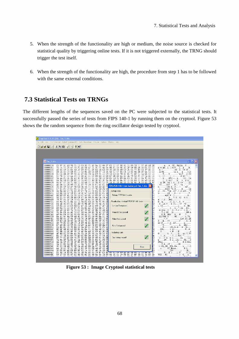
7. Statistical Tests and Analysis
5. When the strength of the functionality are high or medium, the noise source is checked for
statistical quality by triggering online tests. If it is not triggered externally, the TRNG should
trigger the test itself.
6. When the strength of the functionality are high, the procedure from step 1 has to be followed
with the same external conditions.
7.3 Statistical Tests on TRNGs
The different lengths of the sequences saved on the PC were subjected to the statistical tests. It
successfully passed the series of tests from FIPS 140-1 by running them on the cryptool. Figure 53
shows the the random sequence from the ring oscillator design tested by cryptool.
Figure 53 : Image Cryptool statistical tests
68

7. Statistical Tests and Analysis
Tests Max Test value Test Value
Frequency Test 3.841000 0.21235
Poker Test 14.070000 -24325465.679434
Run Test 9.488000 3.536385
Long Run Test 34 26
Serial Test 5.991000 0.191724
Table 3 : Test results FIPS with Ring oscillator design
Figure 54 : Image BSI statistical tests
Figure 54 shows the BSI statistical tests. To begin with the appropriate evaluation class has to be
selected. Then the random sequence file should be loaded and the 8 statistical tests were run
switching the appropriate evaluation classes. It successfully passed all the BSI tests. The random
sequence from the new noise source, the oscillator board was also tested. The sequence was
subjected to the tests FIPS 140-1 and BSI tests and it successfully passed these tests.
69

7. Statistical Tests and Analysis
Tests Max Test value Test Value
Frequency Test 3.841000 0.84321
Poker Test 14.070000 -1003931.024783
Run Test 9.488000 4.690381
Long Run Test 34 25
Serial Test 5.991000 0.440604 Table 4 : Test results FIPS with astable oscillator design
Table 4 shows the results from the FIPS 140-1 tests run on cryptool after digital post processing.
The post processing of the bit stream improved the randomness as observed from the tests. Though
many tests actually failed when the test were run for the sequence without the digital correction.
Hence several tests were run to evaluate the TRNG.
70

8. Conclusion
8. Conclusion
A true random number generator with various noise sources was designed. The random noise
source from the ring oscillator design inside the FPGA and the astable oscillators outside the FPGA
were the sources of randomness for the TRNG. The noise source was sampled, digitally post-
processed and the generated random sequence was transmitted to the PC through the interface
circuitry. The random bit sequence passes the general statistical tests from NIST and BSI.
The aim of our experiments was to test the generation of independent random bits on a hardware
level by manually moving and placing the ring oscillator design on the FPGA. Test for influence of
individual designs when placed on the same FPGA was analysed. From the observations and
experiments, there are definitely a lot of interactions among the ring oscillator placed in the design.
The cross correlation of the two independently placed ring oscillator designs with 200 rings and a
single ring with 27 inverter was tested. But there are a lot of factors that influence the physical
interactions on a hardware level such as electromagnetic interactions, crosstalk etc. The
measurement strategies from the FPGA board also has it own losses. The I/O pins from the FPGAs
and the long measurement probes contribute to the loss of the signal data from the FPGA. Lossless
and accurate measurements is necessary. Direct measurements on the FPGA chip is necessary for
accurate signal measurements, which are quite expensive to carry out. However the jitter analysis
from the ring oscillator designs shows that the jitter curve is periodical in nature showing that they
contribute to interactions in each ring from the inverters when implemented in the FPGA. On the
other hand the jitter plot from the astable oscillator design are non periodical. The non periodicity
from the individual oscillators contributes to independent designs, which is an interesting aspect
considering the ring oscillators.
Future Work
Random number generator design is an exciting field, every year new requirements and designs are
derived and is opposed for flaws and faults in several conferences. It is quite challenging as the
design has to be secure from attacks and should be fault proof. A detailed analysis on the ring
oscillator design can be made with more accurate measurements. More analysis in required on a
physical level with different implementation strategies. To employ for space applications, the
thermal analysis and implementing the design on radiation hard devices has to be carried out.
Redundancy has to be included on the design along with the other systems.
71

8. Conclusion
72

A. Appendix : A.1 AIS 31-BSI Statistical Tests
A. Appendix : A.1 AIS 31-BSI Statistical Tests
(From the Functionality class and evaluation methodology for true (physical) random number
generators – BSI [29])
The statistical test T0 - T5 belongs to the functionality class P1. For example, if the sequence of w1,
w2, w3, ......,w2^16 and b1, b2, b3, ......,b20000 are generated then the rejection probabilities for the tests
are T0 = 2^-1/7 and T1 - T5 = 10^-6. The statistical test T6 - T8 belongs to functionality class P2. For
example, if the sequence of w1, w2, w3,.......,wn and b1, b2, b3, .....,b(Q+K)L are generated then the
rejection probabilities for the tests are negligible for assumed evaluator parameters [29].
T0 Disjointness Test Consider a sequence w1, w2,......,w2^16 ∈ {0,1} 48 will pass the disjointness test if the members of the
sequence are different pairwise.
T1 Monobit TestIt is defined by
consider the sequence b1, b2, b3, ......,b20000 will pass the monobit test if 9654 <X<10346.
T2 Poker TestConsider j = 1,..... 5000 and cj = 8 b4j-3 + 4 b4j-2 + 2b4j-1 + b4j and f[i] := | {j: cj=i}|
The function is defined by
The sequence b1, b2, b3, ......,b20000 will pass the poker test if 1.03<Y<57.4 with 15 degrees of
freedom.
T3 Run TestThe run test as already discussed on the NIST section, is the maximum number of consecutive zeros
and ones of a sequence.
consider the sequence b1, b2, b3, ......,b20000 will pass the run test if the run lengths lies within the
allowed intervals.
Run Length (1) has a permitted interval (2267-2733)
Run Length (2) has a permitted interval (1079-1421)
73
Y =16/5000∑i=0
15
f [i ]²−5000
X =∑j=1
20000
b j

A. Appendix : A.1 AIS 31-BSI Statistical Tests
Run Length (3) has a permitted interval (502-748)
Run Length (4) has a permitted interval (233-402)
Run Length (5) has a permitted interval (90-223)
Run Length (>=6) has a permitted interval (90-233)
T4 Long Run TestThe sequence b1, b2, b3, ......,b20000 will pass the long run test when there is no long run. If a run of
length is above 34, then it is a long run.
T5 Auto Correlation TestConsider τ ∈{1,2,....5000} and
The sequence b1, b2, b3, ......,b20000 will pass the auto correlation test when 2326<Z τ<2674.
T6 Uniform Distribution TestConsider the sequence w1, w2,......,w2^16 ∈ {0,1} k will pass the uniform distribution test if
1n[ jn] [w j=x ]∈ 2−k
−a ,2−ka for all x ∈ {0,1} k
T7 Comparative Test for multinomial distributions Consider the sample wil,... wi,n ∈ for every i {1,...h} assuming the values from the set {0,1,...s-1}.
From null hypothesis, individual samples are identical for multinomial distribution.
For t ∈ {0,1,...s-1} let fi[t]:=|{j: w ij=t}| and pt:=(f1[t]+....fh[t])/(hn) are relative frequency for t of all
samples. By null hypothesis,
∑i=1....h
∑t=0....s−1
f i[ t ]−npt2/np t
It is distributed with (h-1)(s-1) degrees of freedom.
T8 Entropy TestConsider the sequence b1, b2, b3, .....,b(Q+K)L is segmented into non overlapping output words w1, w2,
w3, .....,w(Q+K) of length L. Then An will be the distance from predecessor wn .
An = n if no i<n exist with wn = wn-i
min {i |i>1, wn = wn-i}
It is derived as per Coron test.
74
Zτ=∑
j=1
5000
b jb jτ

A.2 Measurements
A.2 Measurements
Figure A.1 : Ring 27 High,Low and corresponding Ring 200 Measurements(Auto)
75

A.2 Measurements
Figure A.2 : Ring 27 High,Low and corresponding Ring 200 Measurements(Manual)
76

A.3 FPGA Editor Routed Design
A.3 FPGA Editor Routed Design
Figure A.3 : Xilinx FPGA Editor logic resources used, manually placed Ring 200, Ring 27.
77
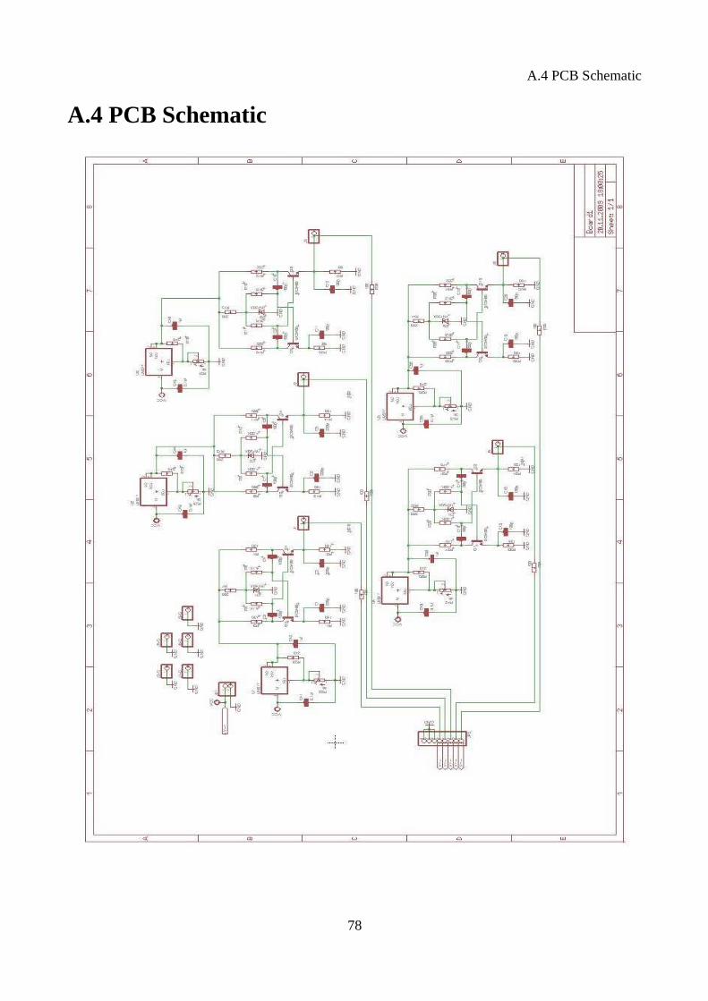
A.4 PCB Schematic
A.4 PCB Schematic
78
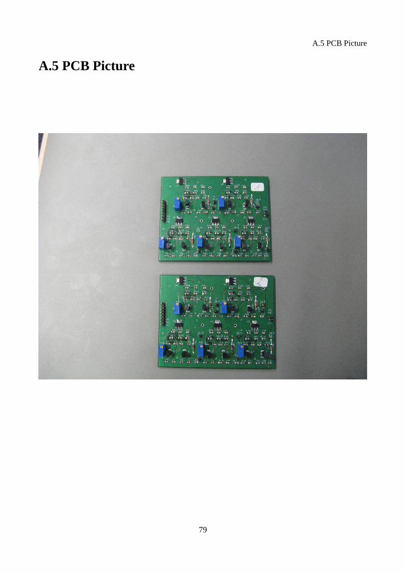
A.5 PCB Picture
A.5 PCB Picture
79

9.Bibliography
9.Bibliography
[1] Cetin Kaya Koc, “Cryptographic Engineering”, Springer, 2008, ISBN : 978-0-387-71816-3.
[2] Eugene R. Hnatek, Practical reliability of electronic equipment and products, Marcel Dekker
Inc, 2003.
[3] Radiation Effects and Analysis, NASA http://radhome.gsfc.nasa.gov/ [Checked : 19 Feb 2010]
[4] Kohlbrenner W.Paul, “The Design and Analysis of a True Random Number Generator in a Field
Programmable Gate Array”, Proc. of International Symposium on FPGAs, 2004.
[5] B. Sunar, W.J. Martin, D.R. Stinson, “A Provably Secure True Random Number Generator
with Built-in Tolerance to Active Attacks”, Proc. of IEEE Transactions on Computers, 2007.
[6] B. Jun and P. Kocher, “The Intel Random Number Generator”, Cryptography research, Inc.
white paper for Intel Corporation, 1999.
[7] B. Chor, O. Goldreich, J. Hastad, “The Bit Extraction Problem or T-Resilient Functions”,
Proc. of FOCS, 1985.
[8] V.Bagini and M.Bucci, “A Design of a Reliable TRNG for Cryptographic Applications”,
Proc. of Cryptographic Hardware and Embedded Systems (CHES) 1999.
[9] T.E.Tkacik, “A Hardware Random Number Generator”, Proc. of CHES 2002.
[10] M. Dichtl and J.Dj. Golic, “High-Speed True Random Number Generation with Logic Gates
Only”, Proc. of CHES 2007.
[11] J.von Neumann, “Various techniques for use in connection with random digits”, Applied
Mathematics Series, 1951.
[12] Fischer and Drutavrovsky, “True random number generator embedded in reconfigurable
hardware”, Proc. of CHES 2002.
[13] Xilinx Inc : “Spartan-3E FPGA Family complete data sheet”, DS312 (v3.7), 2008.
[14] Xilinx Inc : “Spartan-3E Starter kit board user guide”, UG230 (v1.1), 2008.
[15] J. Walrand, “Probability theory and random process” at University of California, 2004
http://walrandpc.eecs.berkeley.edu/126notes.pdf [Checked : 19 Feb 2010]
[16] R.H. Williams, “Electrical Engineering probability”,West Pub., c1991, ISBN : 031479980X.
[17] Tektronix Inc : Application notes, “A guide to understanding and characterizing Timing Jitter”,
2008.
[18] S.K. Yoo, D. Karakoyunlu, B. Birand, B. Sunar, “Improving the Robustness of Ring Oscillator
80

9.Bibliography
TRNGs”, http://ece.wpi.edu/~sunar/preprints/rings.pdf, 2008. [Checked : 19 Feb 2010]
[19] D. Schellekens, B. Preneel, I. Verbauwhede, “FPGA vendor agnostic True Random Number
Generator”, Proc. of Field Programmable Logic and Applications, 2006.
[20] K. Wold and C. H. Tan, “Analysis and enhancement of Random Number Generator in FPGA
Based on Oscillator Rings”, Proc. of Reconfigurable Computing and FPGAs, 2008.
[21] M.S. McClure “Digital Jitter Measurement and Separation”, Thesis work at Texas Technical
University, 2005.
[22] B. Barak, R. Shaltiel, E. Tromer, “True Random Number Generators Secure in a Changing
Environment”, Proc. of CHES 2003.
[23] C. Wright, “So You Need a Random Number Generator”, Oregon State University, 2004.
[24] R. Davies, “Hardware random number generators”, http://www.robertnz.net/hwrng.htm
[Checked : 19 Feb 2010]
[25] V. Fischer, A. Aubert, F. Bernard, B. Valtchanov, J.L. Danger, N. Bochard, “True Random
Number Generators”, Proc. of Configurable Logic Devices, 2009.
[26] Wikimedia Foundation Inc : http://en.wikipedia.org/wiki/Multivibrator [Checked : 19 Feb
2010]
[27] Astable Multivibrator Operation, http://www.falstad.com/circuit/e-multivib-a.html [Checked :
19 Feb 2010]
[28] A.Rukhin et al., “A Statistical Test Suite for Random and Pseudorandom Number Generators
for Cryptographic Applications”, National Institute of Standards and technology, 2001.
[29] W. Killmann, W. Schindler, “A proposal for : Functionality Classes and evaluation
methodology for true (physical) random number generators”, Bundesamt für Sicherheit in
der Informationstechnik, Ver 3.1, 2001.
[30] NASA Office of Logic Design, http://www.klabs.org/index_klabs_dot_org.htm [Checked : 19
Feb 2010]
[31] S. Habinc, “Suitability of reprogrammable FPGAs in space applications”, Gaisler Research
Feasibility Report, 2002.
[32] C. Carmichael, “Triple Module Redundancy Design Techniques for Virtex FPGAs”, Xilinx
Gaisler Research Feasibility Report, 2002.
[33] J.Horst, “Radiation tolerant implementation of a LEON processor for space applications,
University of Stellenbosch, Literature Study, 2005.
[34] Actel Corporation : “Radiation Hardened FPGAs datasheet RH1020, RH1280”, (v3.1) 2005.
81
Abbreviations
Abbreviations
BSI - Bundesamt für Sicherheit in der Informationstechnik
CLB - Configurable Logic Blocks
CRC - Cyclic Redundancy Check
DAS - Digitized Analog Signal
DCM - Digital Clock Manager
DRNG - Deterministic Random Number Generator
DRC - Design Rule Check
EDIF - Electronic Data Interchange Format File
ERC - Electric Rule Check
FIFO - First In First Out
FPGA - Field Programmable Gate Array
HSTL - High Speed Transistor Logic
LVDS - Low Voltage Differential Signaling
LUT - Look up Table
NIST - National Institute of Standards and Technology
NPTRNG - Non-Physical True Random Number Generator
PCB - Printed Circuit Board
PTRNG - Physical True Random Number Generator
RNG - Random Number Generator
RSDS - Reduced Swing Differential Signal
SEU - Single Event Upset
SET - Single Event Transient
SSTL - Stub Series Terminated Logic
TRNG - True Random Number Generator
UART - Universal Asynchronous Receive Transmit
UCF - User Constraints File
VHDL - Very High Speed Integrated Circuit Hardware Description Language
XCorr - Cross Correlation
82

På svenska
Detta dokument hålls tillgängligt på Internet – eller dess framtida ersättare – under en längre tid från
publiceringsdatum under förutsättning att inga extra-ordinära omständigheter uppstår.
Tillgång till dokumentet innebär tillstånd för var och en att läsa, ladda ner, skriva ut enstaka
kopior för enskilt bruk och att använda det oförändrat för ickekommersiell forskning och för
undervisning. Överföring av upphovsrätten vid en senare tidpunkt kan inte upphäva detta tillstånd.
All annan användning av dokumentet kräver upphovsmannens medgivande. För att garantera
äktheten, säkerheten och tillgängligheten finns det lösningar av teknisk och administrativ art.
Upphovsmannens ideella rätt innefattar rätt att bli nämnd som upphovsman I den omfattning
som god sed kräver vid användning av dokumentet på ovan beskrivna sätt samt skydd mot att
dokumentet ändras eller presenteras i sådan form eller i sådant sammanhang som är kränkande för
upphovsmannens litterära eller konstnärliga anseende eller egenart.
För ytterligare information om Linköping University Electronic Press se förlagets hemsida
http://www.ep.liu.se/
In English
The publishers will keep this document online on the Internet - or its possible replacement - for a
considerable time from the date of publication barring exceptional circumstances.
The online availability of the document implies a permanent permission for anyone to read,
to download, to print out single copies for your own use and to use it unchanged for any non-
commercial research and educational purpose. Subsequent transfers of copyright cannot revoke this
permission. All other uses of the document are conditional on the consent of the copyright owner.
The publisher has taken technical and administrative measures to assure authenticity, security and
accessibility.
According to intellectual property law the author has the right to be mentioned when his/her
work is accessed as described above and to be protected against infringement.
For additional information about the Linköping University Electronic Press and its procedures for
publication and for assurance of document integrity, please refer to its WWW home page:
http://www.ep.liu.se/
© Prassanna Shanmuga Sundaram