Embed Size (px)
Citation preview
Copyright ⓒ The Korean Society for Aeronautical & Space SciencesReceived: December 21, 2011 Accepted: April 26, 2012
260 http://ijass.org pISSN: 2093-274x eISSN: 2093-2480
Technical PaperInt’l J. of Aeronautical & Space Sci. 13(2), 260–265 (2012)DOI:10.5139/IJASS.2012.13.2.260
Development of a Fine Digital Sun Sensor for STSAT-2
Sung-Ho Rhee* and Joon Lyou** Satellite Technology Research Center, KAIST, Daejeon 305-701, Korea
Department of Electronics Engineering, Chungnam National University, Daejeon 305-764, Korea
Abstract
Satellite devices for fine attitude control of the Science & Technology Satellite-2 (STSAT-2). Based on the mission requirements
of STSAT-2, the conventional analog-type sun sensors were found to be inadequate, motivating the development of a compact,
fast and fine digital sun sensor (FDSS). The FDSS uses a CMOS image sensor and has an accuracy of less than 0.03degrees, an
update rate of 5Hz and a weight of less than 800g. A pinhole-type aperture is substituted for the optical lens to minimize its
weight. The target process speed is obtained by utilizing the Field Programmable Gate Array (FPGA), which acquires images
from the CMOS sensor, and stores and processes the image data. The sensor accuracy is maintained by a rigorous centroid
algorithm. This paper describes the FDSS designs, realizations, tests and calibration results.
Key words: STSAT-2, FDSS, CMOS-image sensor(CIS), Pinhole-type aperture, Centroid algorithm
1. Introduction
An attitude determination system for satellites is developed
by using the data measured by attitude sensors, such as the
sun sensor (SS), earth horizon sensor (EHS), magnetometer
(MAG), fiber optic gyro (FOG) and star tracker (ST). Among
these sensors, the sun sensors especially have been used
widely to determine coarse and fine attitudes. Analog-type sun
sensors have been developed for Korea Institute Technology
Satellite (KITSAT)-1, 2, 3 and Science & Technology Satellite-1
(STSAT-1) over the past decade. These analog sun sensors
have an accuracy of less than 1 degree.
Based on the mission requirements of STSAT-2, the
conventional analog- type sun sensors were found to be
inadequate, motivating the development of a compact, fast
and fine digital sun sensor (FDSS) [1,2]. The main objective
of the FDSS is precise attitude determination of STSAT-2 for
precision sun pointing missions and new major technology
development projects. The target process speed is obtained
by utilizing the Field Programmable Gate Array (FPGA),
which acquires images from the CMOS sensor, and stores and
processes the image data. The Field Of View (FOV) is 20×20
degrees for each axis. The sensor accuracy is maintained by
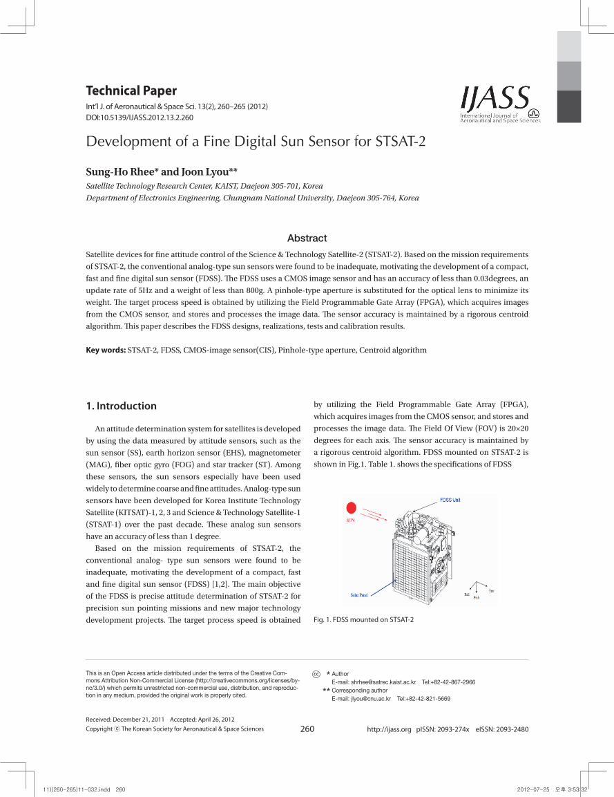
a rigorous centroid algorithm. FDSS mounted on STSAT-2 is
shown in Fig.1. Table 1. shows the specifications of FDSS
Fig. 1. FDSS mounted on STSAT-2
Table 1. Specifications of FDSS
2. Optical Design of FDSS
2.1 Basic principles of FDSS
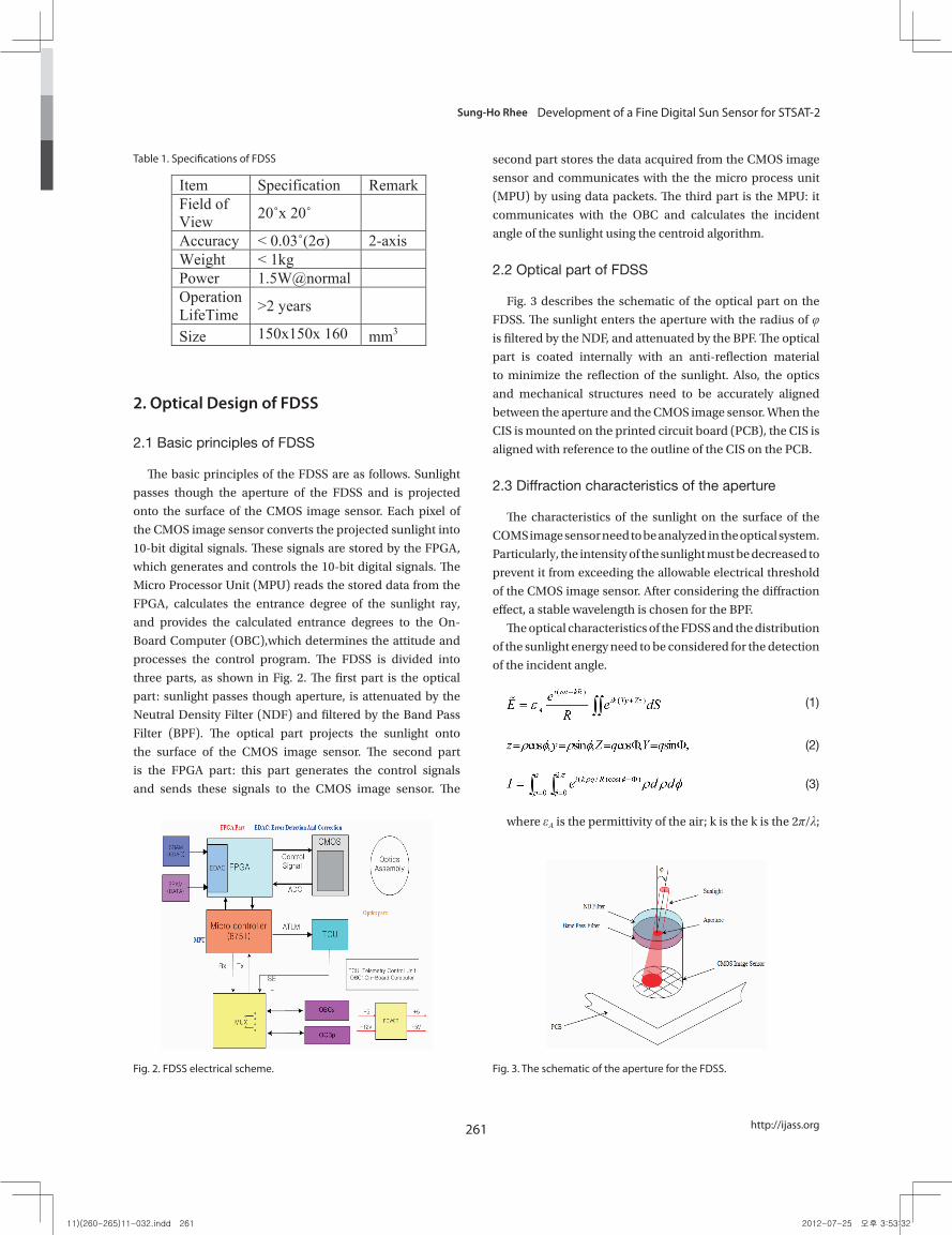
The basic principles of the FDSS are as follows. Sunlight passes though the aperture of the FDSS and is projected onto the surface of the CMOS image sensor. Each pixel of the CMOS image sensor converts the projected sunlight into 10-bit digital signals. These signals are stored by the FPGA, which generates and controls the 10-bit digital signals. The Micro Processor Unit (MPU) reads the stored data from the FPGA, calculates the entrance degree of the sunlight ray, and provides the calculated entrance degrees to the On-Board Computer (OBC),which determines the attitude and processes the control program. The FDSS is divided into three parts, as shown in Fig. 2. The first part is the optical part: sunlight passes though aperture, is attenuated by
the Neutral Density Filter (NDF) and
filtered by the Band Pass Filter (BPF). The optical part projects the sunlight onto the surface of the CMOS image sensor. The second part is the FPGA part: this part generates the control signals and sends these signals to the CMOS image sensor. The second part stores the data acquired from the CMOS image sensor and communicates with the the micro process unit (MPU) by using data packets. The third part is the MPU: it communicates with the OBC and calculates the incident angle of the sunlight using the centroid algorithm.
Fig. 2. FDSS electrical scheme.
Fig. 3. The schematic of the aperture for
the FDSS.
Item Specification Remark Field of View 20x 20 Accuracy < 0.03(2σ) 2-axis Weight < 1kg Power 1.5W@normal Operation LifeTime >2 years Size 150x150x 160 mm3
Fig. 1. FDSS mounted on STSAT-2
This is an Open Access article distributed under the terms of the Creative Com-mons Attribution Non-Commercial License (http://creativecommons.org/licenses/by-nc/3.0/) which permits unrestricted non-commercial use, distribution, and reproduc-tion in any medium, provided the original work is properly cited.
** Author ** E-mail: [email protected] Tel:+82-42-867-2966 ** Corresponding author ** E-mail: [email protected] Tel:+82-42-821-5669
11)(260-265)11-032.indd 260 2012-07-25 오후 3:53:32
261
Sung-Ho Rhee Development of a Fine Digital Sun Sensor for STSAT-2
http://ijass.org
2. Optical Design of FDSS
2.1 Basic principles of FDSS
The basic principles of the FDSS are as follows. Sunlight
passes though the aperture of the FDSS and is projected
onto the surface of the CMOS image sensor. Each pixel of
the CMOS image sensor converts the projected sunlight into
10-bit digital signals. These signals are stored by the FPGA,
which generates and controls the 10-bit digital signals. The
Micro Processor Unit (MPU) reads the stored data from the
FPGA, calculates the entrance degree of the sunlight ray,
and provides the calculated entrance degrees to the On-
Board Computer (OBC),which determines the attitude and
processes the control program. The FDSS is divided into
three parts, as shown in Fig. 2. The first part is the optical
part: sunlight passes though aperture, is attenuated by the
Neutral Density Filter (NDF) and filtered by the Band Pass
Filter (BPF). The optical part projects the sunlight onto
the surface of the CMOS image sensor. The second part
is the FPGA part: this part generates the control signals
and sends these signals to the CMOS image sensor. The
second part stores the data acquired from the CMOS image
sensor and communicates with the the micro process unit
(MPU) by using data packets. The third part is the MPU: it
communicates with the OBC and calculates the incident
angle of the sunlight using the centroid algorithm.
2.2 Optical part of FDSS
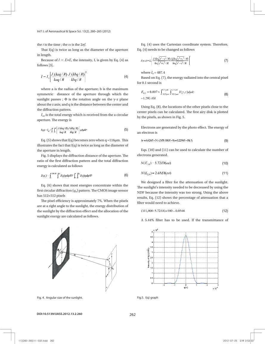
Fig. 3 describes the schematic of the optical part on the
FDSS. The sunlight enters the aperture with the radius of φ
is filtered by the NDF, and attenuated by the BPF. The optical
part is coated internally with an anti-reflection material
to minimize the reflection of the sunlight. Also, the optics
and mechanical structures need to be accurately aligned
between the aperture and the CMOS image sensor. When the
CIS is mounted on the printed circuit board (PCB), the CIS is
aligned with reference to the outline of the CIS on the PCB.
2.3 Diffraction characteristics of the aperture
The characteristics of the sunlight on the surface of the
COMS image sensor need to be analyzed in the optical system.
Particularly, the intensity of the sunlight must be decreased to
prevent it from exceeding the allowable electrical threshold
of the CMOS image sensor. After considering the diffraction
effect, a stable wavelength is chosen for the BPF.
The optical characteristics of the FDSS and the distribution
of the sunlight energy need to be considered for the detection
of the incident angle.
(1)
(2)
(3)
where εA is the permittivity of the air; k is the k is the 2π/λ;
Table 1. Specifications of FDSS
Fig. 1. FDSS mounted on STSAT-2
Table 1. Specifications of FDSS
2. Optical Design of FDSS
2.1 Basic principles of FDSS
The basic principles of the FDSS are as follows. Sunlight passes though the aperture of the FDSS and is projected onto the surface of the CMOS image sensor. Each pixel of the CMOS image sensor converts the projected sunlight into 10-bit digital signals. These signals are stored by the FPGA, which generates and controls the 10-bit digital signals. The Micro Processor Unit (MPU) reads the stored data from the FPGA, calculates the entrance degree of the sunlight ray, and provides the calculated entrance degrees to the On-Board Computer (OBC),which determines the attitude and processes the control program. The FDSS is divided into three parts, as shown in Fig. 2. The first part is the optical part: sunlight passes though aperture, is attenuated by
the Neutral Density Filter (NDF) and
filtered by the Band Pass Filter (BPF). The optical part projects the sunlight onto the surface of the CMOS image sensor. The second part is the FPGA part: this part generates the control signals and sends these signals to the CMOS image sensor. The second part stores the data acquired from the CMOS image sensor and communicates with the the micro process unit (MPU) by using data packets. The third part is the MPU: it communicates with the OBC and calculates the incident angle of the sunlight using the centroid algorithm.
Fig. 2. FDSS electrical scheme.
Fig. 3. The schematic of the aperture for
the FDSS.
Item Specification Remark Field of View 20x 20 Accuracy < 0.03(2σ) 2-axis Weight < 1kg Power 1.5W@normal Operation LifeTime >2 years Size 150x150x 160 mm3
Fig. 1. FDSS mounted on STSAT-2
Table 1. Specifications of FDSS
2. Optical Design of FDSS
2.1 Basic principles of FDSS
The basic principles of the FDSS are as follows. Sunlight passes though the aperture of the FDSS and is projected onto the surface of the CMOS image sensor. Each pixel of the CMOS image sensor converts the projected sunlight into 10-bit digital signals. These signals are stored by the FPGA, which generates and controls the 10-bit digital signals. The Micro Processor Unit (MPU) reads the stored data from the FPGA, calculates the entrance degree of the sunlight ray, and provides the calculated entrance degrees to the On-Board Computer (OBC),which determines the attitude and processes the control program. The FDSS is divided into three parts, as shown in Fig. 2. The first part is the optical part: sunlight passes though aperture, is attenuated by
the Neutral Density Filter (NDF) and
filtered by the Band Pass Filter (BPF). The optical part projects the sunlight onto the surface of the CMOS image sensor. The second part is the FPGA part: this part generates the control signals and sends these signals to the CMOS image sensor. The second part stores the data acquired from the CMOS image sensor and communicates with the the micro process unit (MPU) by using data packets. The third part is the MPU: it communicates with the OBC and calculates the incident angle of the sunlight using the centroid algorithm.
Fig. 2. FDSS electrical scheme.
Fig. 3. The schematic of the aperture for
the FDSS.
Item Specification Remark Field of View 20x 20 Accuracy < 0.03(2σ) 2-axis Weight < 1kg Power 1.5W@normal Operation LifeTime >2 years Size 150x150x 160 mm3
Fig. 2. FDSS electrical scheme.
Fig. 1. FDSS mounted on STSAT-2
Table 1. Specifications of FDSS
2. Optical Design of FDSS
2.1 Basic principles of FDSS
The basic principles of the FDSS are as follows. Sunlight passes though the aperture of the FDSS and is projected onto the surface of the CMOS image sensor. Each pixel of the CMOS image sensor converts the projected sunlight into 10-bit digital signals. These signals are stored by the FPGA, which generates and controls the 10-bit digital signals. The Micro Processor Unit (MPU) reads the stored data from the FPGA, calculates the entrance degree of the sunlight ray, and provides the calculated entrance degrees to the On-Board Computer (OBC),which determines the attitude and processes the control program. The FDSS is divided into three parts, as shown in Fig. 2. The first part is the optical part: sunlight passes though aperture, is attenuated by
the Neutral Density Filter (NDF) and
filtered by the Band Pass Filter (BPF). The optical part projects the sunlight onto the surface of the CMOS image sensor. The second part is the FPGA part: this part generates the control signals and sends these signals to the CMOS image sensor. The second part stores the data acquired from the CMOS image sensor and communicates with the the micro process unit (MPU) by using data packets. The third part is the MPU: it communicates with the OBC and calculates the incident angle of the sunlight using the centroid algorithm.
Fig. 2. FDSS electrical scheme.
Fig. 3. The schematic of the aperture for
the FDSS.
Item Specification Remark Field of View 20x 20 Accuracy < 0.03(2σ) 2-axis Weight < 1kg Power 1.5W@normal Operation LifeTime >2 years Size 150x150x 160 mm3
Fig. 3. The schematic of the aperture for the FDSS.
11)(260-265)11-032.indd 261 2012-07-25 오후 3:53:32
DOI:10.5139/IJASS.2012.13.2.260 262
Int’l J. of Aeronautical & Space Sci. 13(2), 260–265 (2012)
the t is the time ; the ω is the 2πf.That I(q) is twice as long as the diameter of the aperture
in length.
Because of I ∝ E*E, the intensity, I, is given by Eq. (4) as
follows [3].
(4)
where a is the radius of the aperture; b is the maximum
symmetric distance of the aperture through which the
sunlight passes ; Φ is the rotation angle on the y-z plane
about the z axis; and q is the distance between the center and
the diffraction pattern.
Itot is the total energy which is received from the a circular
aperture. The energy is
(5)
Eq. (5) shows that I(q) becomes zero when q =116µm. This
illustrates the fact that I(q) is twice as long as the diameter of
the aperture in length.
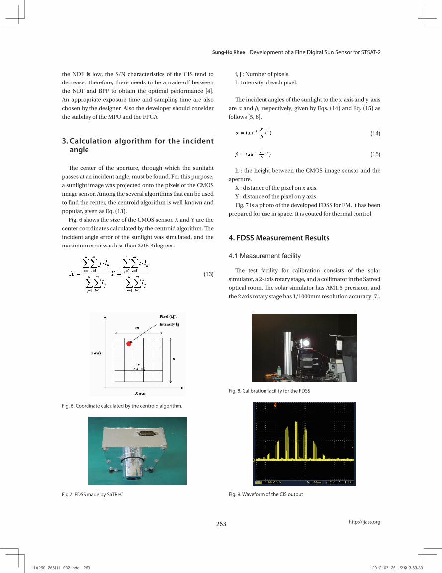
Fig. 5 displays the diffraction distance of the aperture. The
ratio of the first diffraction pattern and the total diffraction
energy is calculated as follows
(6)
Eq. (6) shows that most energies concentrate within the
first circular diffraction (q0) pattern. The CMOS image sensor
has 512×512 pixels
The pixel efficiency is approximately 7%. When the pixels
are at a right angle to the sunlight, the energy distribution of
the sunlight by the diffraction effect and the allocation of the
sunlight energy are calculated as follows.
Eq. (4) uses the Cartesian coordinate system. Therefore,
Eq. (4) needs to be changed as follows
(7)
where I0 = 487.4
Based on Eq. (7), the energy radiated into the central pixel
for 0.1 second is
(8)
Using Eq. (8), the locations of the other pixels close to the
center pixels can be calculated. The first airy disk is plotted
by the pixels, as shown in Fig. 5.
Electrons are generated by the photo effect. The energy of
an electron is
(9)
Eqs. (10) and (11) can be used to calculate the number of
electrons generated.
(10)
(11)
We designed a filter for the attenuation of the sunlight.
The sunlight’s intensity needed to be decreased by using the
NDF because the intensity was too strong. Using the above
results, Eq. (12) shows the percentage of attenuation that a
filter would need to achieve.
(12)
A 5.44% filter has to be used. If the transmittance of
2.2 Optical part of FDSS
Fig. 3 describes the schematic of the optical part on the FDSS. The sunlight enters the aperture with the radius of φ is filtered by the NDF, and attenuated by the BPF. The optical part is coated internally with an anti-reflection material to minimize the reflection of the sunlight. Also, the optics and mechanical structures need to be accurately aligned between the aperture and the CMOS image sensor. When the CIS is mounted on the printed circuit board (PCB), the CIS is aligned with reference to the outline of the CIS on the PCB.
2.3 Diffraction characteristics of the aperture
The characteristics of the sunlight on the surface of the COMS image sensor need to be analyzed in the optical system. Particularly, the intensity of the sunlight must be decreased to prevent it from exceeding the allowable electrical threshold of the CMOS image sensor. After considering the diffraction effect, a stable wavelength is chosen for the BPF.
The optical characteristics of the FDSS and the distribution of the sunlight energy need to be considered for the detection of the incident angle.
( )( )
i t kRik Yy Zz
AeE e dS
R
ω
ε−
+= ∫∫% (1)
cos , sin , cos , sinz y Z q Y qρ φ ρ φ= = = Φ = Φ, (2)
2 ( / )cos( )
0 0
a i k q RI e d dπ ρ φ
ρ φρ ρ φ−Φ
= == ∫ ∫ (3)
where Aε is the permittivity of the air; k is the k is the 2π λ ; the t is the time ; the ω is the 2 fπ .
That I(q) is twice as long as the diameter of the aperture in length.
Fig. 4. Angular size of the sunlight.
Because of I E E∝ ∗ , the intensity, I, is given by Eq. (4) as follows [3].
2
1 10
( / ) ( / )/ /
J kaq R J kbq RI Ikaq R kbq R
= (4)
where a is the radius of the aperture; b
is the maximum symmetric distance of the aperture through which the sunlight passes ; Φ is the rotation angle on the y-z plane about the z axis; and q is the distance between the center and the diffraction pattern.
totI is the total energy which is received from the a circular aperture. The energy is
22
1 10 0
( / ) ( / )( ) // /tot
J kaq R J kbq RI q I qdqdkaq R kbq R
πθ
∞ ⎡ ⎤= ⎢ ⎥
⎣ ⎦∫ ∫ , (5)
Eq. (5) shows that I(q) becomes zero
when q =116µm. This illustrates the fact that I(q) is twice as long as the diameter of the aperture in length.
Fig. 4. Angular size of the sunlight.
Fig.5. I(q) graph Fig. 5 displays the diffraction distance
of the aperture. The ratio of the first diffraction pattern and the total diffraction energy is calculated as follows
0.000116 2 2
0 0 0 0 0( ) ( ) / ( )I q I q qdqd I q qdqd
π πθ θ
∞=∫ ∫ ∫ ∫ (6)
Eq. (6) shows that most energies
concentrate within the first circular diffraction 0( )q pattern. The CMOS image
sensor has 512 512× pixels The pixel efficiency is approximately
7%. When the pixels are at a right angle to the sunlight, the energy distribution of the sunlight by the diffraction effect and the allocation of the sunlight energy are calculated as follows.
Eq. (4) uses the Cartesian coordinate system. Therefore, Eq. (4) needs to be changed as follows
22 2 2 2
1 10 2 2 2 2
( / ) ( / )( , )
/ /
J ka y z R J ka y z RI y z I
ka y z R ka y z R
⎡ ⎤+ += ⎢ ⎥
⎢ + + ⎥⎣ ⎦
(7)
where 0 487.4I =
Based on Eq. (7), the energy radiated into the central pixel for 0.1 second is
12.5 12.5
0,0 12.5 12.50.007 ( , )
m m
m mE I y z dydz
μ μ
μ μ− −= × ∫ ∫
1.29E-10J= (8)
Using Eq. (8), the locations of the other pixels close to the center pixels can be calculated. The first airy disk is plotted by the pixels, as shown in Fig. 5.
Electrons are generated by the photo effect. The energy of an electron is
(9)
Eqs. (10) and (11) can be used to calculate the number of electrons generated.
0,0( ) 5.72 8( )N E E ea= (10)
2,0( ) 2.65 8( )N E E ea= (11)
We designed a filter for the attenuation of the sunlight. The sunlight’s intensity needed to be decreased by using the NDF because the intensity was too strong. Using the above results, Eq. (12) shows the percentage of attenuation that a filter would need to achieve. (311,000 / 5.72 8) 100 0.0544E × = (12)
A 5.44% filter has to be used. If the transmittance of the NDF is low, the S/N characteristics of the CIS tend to decrease. Therefore, there needs to be a trade-off between the NDF and BPF to obtain the optimal performance [4]. An appropriate exposure time and sampling time are also chosen by the designer. Also the developer should consider the stability of the MPU and the FPGA
6.626 34 (3 8/880 9) 0.2259 18( )h E E E E Jν = − × − = −
Fig.5. I(q) graph
11)(260-265)11-032.indd 262 2012-07-25 오후 3:53:33
263
Sung-Ho Rhee Development of a Fine Digital Sun Sensor for STSAT-2
http://ijass.org
the NDF is low, the S/N characteristics of the CIS tend to
decrease. Therefore, there needs to be a trade-off between
the NDF and BPF to obtain the optimal performance [4].
An appropriate exposure time and sampling time are also
chosen by the designer. Also the developer should consider
the stability of the MPU and the FPGA
3. Calculation algorithm for the incident angle
The center of the aperture, through which the sunlight
passes at an incident angle, must be found. For this purpose,
a sunlight image was projected onto the pixels of the CMOS
image sensor. Among the several algorithms that can be used
to find the center, the centroid algorithm is well-known and
popular, given as Eq. (13).
Fig. 6 shows the size of the CMOS sensor. X and Y are the
center coordinates calculated by the centroid algorithm. The
incident angle error of the sunlight was simulated, and the
maximum error was less than 2.0E-4degrees.
(13)
i, j : Number of pixels.
l : Intensity of each pixel.
The incident angles of the sunlight to the x-axis and y-axis
are α and β, respectively, given by Eqs. (14) and Eq. (15) as
follows [5, 6].
(14)
(15)
h : the height between the CMOS image sensor and the
aperture.
X : distance of the pixel on x axis.
Y : distance of the pixel on y axis.
Fig. 7 is a photo of the developed FDSS for FM. It has been
prepared for use in space. It is coated for thermal control.
4. FDSS Measurement Results
4.1 Measurement facility
The test facility for calibration consists of the solar
simulator, a 2-axis rotary stage, and a collimator in the Satreci
optical room. The solar simulator has AM1.5 precision, and
the 2 axis rotary stage has 1/1000mm resolution accuracy [7].
3. Calculation algorithm for the incident angle
The center of the aperture, through which the sunlight passes at an incident angle, must be found. For this purpose, a sunlight image was projected onto the pixels of the CMOS image sensor. Among the several algorithms that can be used to find the center, the centroid algorithm is well-known and popular, given as Eq. (13).
Fig. 6. Coordinate calculated by the centroid algorithm.
Fig. 6 shows the size of the CMOS
sensor. X and Y are the center coordinates calculated by the centroid algorithm. The incident angle error of the sunlight was simulated, and the maximum error was less than 2.0E-4degrees.
1 1 1 1
1 1 1 1
n m n m
ij ijj i j i
n m n m
ij ijj i j i
j l i lX Y
l l
= = = =
= = = =
⋅ ⋅= =∑∑ ∑∑
∑∑ ∑∑ (13)
i, j : Number of pixels. l : Intensity of each pixel. The incident angles of the sunlight to
the x-axis and y-axis are α and β, respectively, given by Eqs. (14) and Eq. (15) as follows [5, 6].
1tan ( )Xh
α −= o (14)
1ta n ( )Yh
β −= o (15)
h : the height between the CMOS image sensor and the aperture.
X : distance of the pixel on x axis. Y : distance of the pixel on y axis.
Fig.7. FDSS made by SaTReC Fig. 7 is a photo of the developed
FDSS for FM. It has been prepared for use in space. It is coated for thermal control.
4. FDSS Measurement Results
4.1 Measurement facility
The test facility for calibration consists of the solar simulator, a 2-axis rotary stage, and a collimator in the Satreci optical room. The solar simulator has AM1.5 precision, and the 2 axis rotary stage has 1/1000mm resolution accuracy [7]. Fig. 8 shows the calibration facility of SI (SaTReC Initiative) for the FDSS.
Fig. 8. Calibration facility for the FDSS
Fig. 6. Coordinate calculated by the centroid algorithm.
3. Calculation algorithm for the incident angle
The center of the aperture, through which the sunlight passes at an incident angle, must be found. For this purpose, a sunlight image was projected onto the pixels of the CMOS image sensor. Among the several algorithms that can be used to find the center, the centroid algorithm is well-known and popular, given as Eq. (13).
Fig. 6. Coordinate calculated by the centroid algorithm.
Fig. 6 shows the size of the CMOS
sensor. X and Y are the center coordinates calculated by the centroid algorithm. The incident angle error of the sunlight was simulated, and the maximum error was less than 2.0E-4degrees.
1 1 1 1
1 1 1 1
n m n m
ij ijj i j i
n m n m
ij ijj i j i
j l i lX Y
l l
= = = =
= = = =
⋅ ⋅= =∑∑ ∑∑
∑∑ ∑∑ (13)
i, j : Number of pixels. l : Intensity of each pixel. The incident angles of the sunlight to
the x-axis and y-axis are α and β, respectively, given by Eqs. (14) and Eq. (15) as follows [5, 6].
1tan ( )Xh
α −= o (14)
1ta n ( )Yh
β −= o (15)
h : the height between the CMOS image sensor and the aperture.
X : distance of the pixel on x axis. Y : distance of the pixel on y axis.
Fig.7. FDSS made by SaTReC Fig. 7 is a photo of the developed
FDSS for FM. It has been prepared for use in space. It is coated for thermal control.
4. FDSS Measurement Results
4.1 Measurement facility
The test facility for calibration consists of the solar simulator, a 2-axis rotary stage, and a collimator in the Satreci optical room. The solar simulator has AM1.5 precision, and the 2 axis rotary stage has 1/1000mm resolution accuracy [7]. Fig. 8 shows the calibration facility of SI (SaTReC Initiative) for the FDSS.
Fig. 8. Calibration facility for the FDSS Fig. 8. Calibration facility for the FDSS
3. Calculation algorithm for the incident angle
The center of the aperture, through which the sunlight passes at an incident angle, must be found. For this purpose, a sunlight image was projected onto the pixels of the CMOS image sensor. Among the several algorithms that can be used to find the center, the centroid algorithm is well-known and popular, given as Eq. (13).
Fig. 6. Coordinate calculated by the centroid algorithm.
Fig. 6 shows the size of the CMOS
sensor. X and Y are the center coordinates calculated by the centroid algorithm. The incident angle error of the sunlight was simulated, and the maximum error was less than 2.0E-4degrees.
1 1 1 1
1 1 1 1
n m n m
ij ijj i j i
n m n m
ij ijj i j i
j l i lX Y
l l
= = = =
= = = =
⋅ ⋅= =∑∑ ∑∑
∑∑ ∑∑ (13)
i, j : Number of pixels. l : Intensity of each pixel. The incident angles of the sunlight to
the x-axis and y-axis are α and β, respectively, given by Eqs. (14) and Eq. (15) as follows [5, 6].
1tan ( )Xh
α −= o (14)
1ta n ( )Yh
β −= o (15)
h : the height between the CMOS image sensor and the aperture.
X : distance of the pixel on x axis. Y : distance of the pixel on y axis.
Fig.7. FDSS made by SaTReC Fig. 7 is a photo of the developed
FDSS for FM. It has been prepared for use in space. It is coated for thermal control.
4. FDSS Measurement Results
4.1 Measurement facility
The test facility for calibration consists of the solar simulator, a 2-axis rotary stage, and a collimator in the Satreci optical room. The solar simulator has AM1.5 precision, and the 2 axis rotary stage has 1/1000mm resolution accuracy [7]. Fig. 8 shows the calibration facility of SI (SaTReC Initiative) for the FDSS.
Fig. 8. Calibration facility for the FDSS
Fig.7. FDSS made by SaTReC
4.2 Signal of the CIS outpu
Fig. 9. Waveform of the CIS output
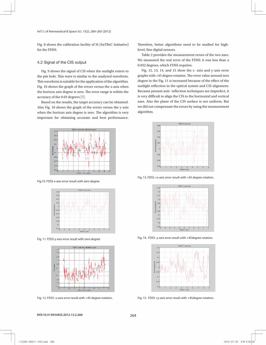
Fig. 9 shows the signal of CIS when the sunlight enters to the pin hole. This wave is similar to the analyzed waveform. This waveform is suitable for the application of the algorithm. Fig. 10 shows the graph of the errors versus the x-axis when the horizon axis degree is zero. The error range is within the accuracy of the 0.03 degrees [7].
Fig.10. FDSS x-axis error result with zero degree
Based on the results, the target
accuracy can be obtained. Also Fig. 10 shows the graph of the errors versus the y-axis when the horizon axis degree is zero. The algorithm is very important for obtaining accurate and best performance. Therefore, better algorithms need to be studied for high-level, fine digital sensors.
Fig. 11. FDSS y-axis error result with zero degree
Fig. 12. FDSS -x-axis error result with +45 degree rotation.
Table 2 provides the measurement errors of the two axes. We measured the real error of the FDSS; it was less than a 0.032 degrees, which FDSS requires.
0 1 2 3 4 5 6 7 8 9-0.06
-0.04
-0.02
0
0.02
0.04
0.06
0.08 FDSS X -axis error
FDSS X -axis
Err
or=
ang-
poly
val
Fig. 13. FDSS +x-axis error result with +45 degree rotation.
-10 -9 -8 -7 -6 -5 -4 -3 -2 -1 0-0.12
-0.1
-0.08
-0.06
-0.04
-0.02
0
0.02
0.04
0.06
0.08 FDSS X -axis error
FDSS X -axis
Err
or=
ang-
poly
val
Fig. 9. Waveform of the CIS output
11)(260-265)11-032.indd 263 2012-07-25 오후 3:53:33
DOI:10.5139/IJASS.2012.13.2.260 264
Int’l J. of Aeronautical & Space Sci. 13(2), 260–265 (2012)
Fig. 8 shows the calibration facility of SI (SaTReC Initiative)
for the FDSS.
4.2 Signal of the CIS output
Fig. 9 shows the signal of CIS when the sunlight enters to
the pin hole. This wave is similar to the analyzed waveform.
This waveform is suitable for the application of the algorithm.
Fig. 10 shows the graph of the errors versus the x-axis when
the horizon axis degree is zero. The error range is within the
accuracy of the 0.03 degrees [7].
Based on the results, the target accuracy can be obtained.
Also Fig. 10 shows the graph of the errors versus the y-axis
when the horizon axis degree is zero. The algorithm is very
important for obtaining accurate and best performance.
Therefore, better algorithms need to be studied for high-
level, fine digital sensors.
Table 2 provides the measurement errors of the two axes.
We measured the real error of the FDSS; it was less than a
0.032 degrees, which FDSS requires.
Fig. 12, 13, 14, and 15 show the x -axis and y-axis error
graphs with +45 degree rotation. The error value around zero
degree in the Fig. 11 is increased because of the effect of the
sunlight reflection in the optical system and CIS alignment.
Because present anti- reflection techniques are imperfect, it
is very difficult to align the CIS to the horizontal and vertical
axes. Also the plane of the CIS surface is not uniform. But
we did not compensate the errors by using the measurement
algorithm.
4.2 Signal of the CIS outpu
Fig. 9. Waveform of the CIS output
Fig. 9 shows the signal of CIS when the sunlight enters to the pin hole. This wave is similar to the analyzed waveform. This waveform is suitable for the application of the algorithm. Fig. 10 shows the graph of the errors versus the x-axis when the horizon axis degree is zero. The error range is within the accuracy of the 0.03 degrees [7].
Fig.10. FDSS x-axis error result with zero degree
Based on the results, the target
accuracy can be obtained. Also Fig. 10 shows the graph of the errors versus the y-axis when the horizon axis degree is zero. The algorithm is very important for obtaining accurate and best performance. Therefore, better algorithms need to be studied for high-level, fine digital sensors.
Fig. 11. FDSS y-axis error result with zero degree
Fig. 12. FDSS -x-axis error result with +45 degree rotation.
Table 2 provides the measurement errors of the two axes. We measured the real error of the FDSS; it was less than a 0.032 degrees, which FDSS requires.
0 1 2 3 4 5 6 7 8 9-0.06
-0.04
-0.02
0
0.02
0.04
0.06
0.08 FDSS X -axis error
FDSS X -axis
Err
or=
ang-
poly
val
Fig. 13. FDSS +x-axis error result with +45 degree rotation.
-10 -9 -8 -7 -6 -5 -4 -3 -2 -1 0-0.12
-0.1
-0.08
-0.06
-0.04
-0.02
0
0.02
0.04
0.06
0.08 FDSS X -axis error
FDSS X -axis
Err
or=
ang-
poly
val
Fig.10. FDSS x-axis error result with zero degree
4.2 Signal of the CIS outpu
Fig. 9. Waveform of the CIS output
Fig. 9 shows the signal of CIS when the sunlight enters to the pin hole. This wave is similar to the analyzed waveform. This waveform is suitable for the application of the algorithm. Fig. 10 shows the graph of the errors versus the x-axis when the horizon axis degree is zero. The error range is within the accuracy of the 0.03 degrees [7].
Fig.10. FDSS x-axis error result with zero degree
Based on the results, the target
accuracy can be obtained. Also Fig. 10 shows the graph of the errors versus the y-axis when the horizon axis degree is zero. The algorithm is very important for obtaining accurate and best performance. Therefore, better algorithms need to be studied for high-level, fine digital sensors.
Fig. 11. FDSS y-axis error result with zero degree
Fig. 12. FDSS -x-axis error result with +45 degree rotation.
Table 2 provides the measurement errors of the two axes. We measured the real error of the FDSS; it was less than a 0.032 degrees, which FDSS requires.
0 1 2 3 4 5 6 7 8 9-0.06
-0.04
-0.02
0
0.02
0.04
0.06
0.08 FDSS X -axis error
FDSS X -axis
Err
or=
ang-
poly
val
Fig. 13. FDSS +x-axis error result with +45 degree rotation.
-10 -9 -8 -7 -6 -5 -4 -3 -2 -1 0-0.12
-0.1
-0.08
-0.06
-0.04
-0.02
0
0.02
0.04
0.06
0.08 FDSS X -axis error
FDSS X -axis
Err
or=
ang-
poly
val
Fig. 12. FDSS -x-axis error result with +45 degree rotation.
-10 -9 -8 -7 -6 -5 -4 -3 -2 -1 0-0.25
-0.2
-0.15
-0.1
-0.05
0
0.05
0.1
0.15
0.2
0.25 FDSS Y -axis error
FDSS Y -axis
Err
or=a
ng-p
olyv
al
Fig. 14. FDSS -y-axis error result with +45degree rotation.
Fig. 15. FDSS +y-axis error result with +45degree rotation.
Fig. 12, 13, 14, and 15 show the x -axis and y-axis error graphs with +45 degree rotation. The error value around zero degree in the Fig. 11 is increased because of the effect of the sunlight reflection in the optical system and CIS alignment. Because present anti- reflection techniques are imperfect, it is very difficult to align the CIS to the horizontal and vertical axes. Also the plane of the CIS surface is not uniform. But we did not compensate the errors by using the measurement algorithm. 5. Conclusion
The incident characteristics of sunlight for the FDSS have been analyzed. After considering the results of the analysis and
simulation, we designed, manufactured, tested, and calibrated the FDSS successfully.
The feasibility of the developed FDSS was verified by now. But the errors, which are affected by factors such as temperature, power characteristics and the Fixed Pattern Noise (FPN) of the CIS, and real measurement algorithm, were considered.
Especially, error compensations ac-cording to a certain range of angles were considered. Also the performance test of FDSS needs to be verified by an orbit test of the STSAT-2. On orbit the test can be tested by the star sensor which has with the accuracy less than 0.016degree.
Unfortunately, the performance mission of this FDSS could not be tested in orbit because of the two times launch failures of KSLV-1 (Korea Space Launch Vehicle-I).
Acknowledgement
This work was supported by the STSAT-2 development project. The author also thanks the Power and Sensor team, the Attitude Determination and Control System team, and SI.
References
[[1] Ok, G., Sun sensor manufacturing for Satellite on study, M.S. thesis, KAIST, Daejeon, South Korea, 1993, pp. 1-30. [2] Hales, J. H., and Pedersen, M., “Two-axes MOEMS Sun Sensor for Pico Satellites”, Proc. of the 16th Annual AIAAA/USU Conference on Small Satellites, Logan, USA, 2002.
0 1 2 3 4 5 6 7 8 9-0.2
-0.15
-0.1
-0.05
0
0.05
0.1
0.15
0.2 FDSS Y -axis error
FDSS Y -axis
Err
or=a
ng-p
olyv
al
Fig. 15. FDSS +y-axis error result with +45degree rotation.
4.2 Signal of the CIS outpu
Fig. 9. Waveform of the CIS output
Fig. 9 shows the signal of CIS when the sunlight enters to the pin hole. This wave is similar to the analyzed waveform. This waveform is suitable for the application of the algorithm. Fig. 10 shows the graph of the errors versus the x-axis when the horizon axis degree is zero. The error range is within the accuracy of the 0.03 degrees [7].
Fig.10. FDSS x-axis error result with zero degree
Based on the results, the target
accuracy can be obtained. Also Fig. 10 shows the graph of the errors versus the y-axis when the horizon axis degree is zero. The algorithm is very important for obtaining accurate and best performance. Therefore, better algorithms need to be studied for high-level, fine digital sensors.
Fig. 11. FDSS y-axis error result with zero degree
Fig. 12. FDSS -x-axis error result with +45 degree rotation.
Table 2 provides the measurement errors of the two axes. We measured the real error of the FDSS; it was less than a 0.032 degrees, which FDSS requires.
0 1 2 3 4 5 6 7 8 9-0.06
-0.04
-0.02
0
0.02
0.04
0.06
0.08 FDSS X -axis error
FDSS X -axis
Err
or=
ang-
poly
val
Fig. 13. FDSS +x-axis error result with +45 degree rotation.
-10 -9 -8 -7 -6 -5 -4 -3 -2 -1 0-0.12
-0.1
-0.08
-0.06
-0.04
-0.02
0
0.02
0.04
0.06
0.08 FDSS X -axis error
FDSS X -axis
Err
or=
ang-
poly
val
Fig. 11. FDSS y-axis error result with zero degree
-10 -9 -8 -7 -6 -5 -4 -3 -2 -1 0-0.25
-0.2
-0.15
-0.1
-0.05
0
0.05
0.1
0.15
0.2
0.25 FDSS Y -axis error
FDSS Y -axis
Err
or=a
ng-p
olyv
al
Fig. 14. FDSS -y-axis error result with +45degree rotation.
Fig. 15. FDSS +y-axis error result with +45degree rotation.
Fig. 12, 13, 14, and 15 show the x -axis and y-axis error graphs with +45 degree rotation. The error value around zero degree in the Fig. 11 is increased because of the effect of the sunlight reflection in the optical system and CIS alignment. Because present anti- reflection techniques are imperfect, it is very difficult to align the CIS to the horizontal and vertical axes. Also the plane of the CIS surface is not uniform. But we did not compensate the errors by using the measurement algorithm. 5. Conclusion
The incident characteristics of sunlight for the FDSS have been analyzed. After considering the results of the analysis and
simulation, we designed, manufactured, tested, and calibrated the FDSS successfully.
The feasibility of the developed FDSS was verified by now. But the errors, which are affected by factors such as temperature, power characteristics and the Fixed Pattern Noise (FPN) of the CIS, and real measurement algorithm, were considered.
Especially, error compensations ac-cording to a certain range of angles were considered. Also the performance test of FDSS needs to be verified by an orbit test of the STSAT-2. On orbit the test can be tested by the star sensor which has with the accuracy less than 0.016degree.
Unfortunately, the performance mission of this FDSS could not be tested in orbit because of the two times launch failures of KSLV-1 (Korea Space Launch Vehicle-I).
Acknowledgement
This work was supported by the STSAT-2 development project. The author also thanks the Power and Sensor team, the Attitude Determination and Control System team, and SI.
References
[[1] Ok, G., Sun sensor manufacturing for Satellite on study, M.S. thesis, KAIST, Daejeon, South Korea, 1993, pp. 1-30. [2] Hales, J. H., and Pedersen, M., “Two-axes MOEMS Sun Sensor for Pico Satellites”, Proc. of the 16th Annual AIAAA/USU Conference on Small Satellites, Logan, USA, 2002.
0 1 2 3 4 5 6 7 8 9-0.2
-0.15
-0.1
-0.05
0
0.05
0.1
0.15
0.2 FDSS Y -axis error
FDSS Y -axis
Err
or=a
ng-p
olyv
al
Fig. 14. FDSS -y-axis error result with +45degree rotation.
4.2 Signal of the CIS outpu
Fig. 9. Waveform of the CIS output
Fig. 9 shows the signal of CIS when the sunlight enters to the pin hole. This wave is similar to the analyzed waveform. This waveform is suitable for the application of the algorithm. Fig. 10 shows the graph of the errors versus the x-axis when the horizon axis degree is zero. The error range is within the accuracy of the 0.03 degrees [7].
Fig.10. FDSS x-axis error result with zero degree
Based on the results, the target
accuracy can be obtained. Also Fig. 10 shows the graph of the errors versus the y-axis when the horizon axis degree is zero. The algorithm is very important for obtaining accurate and best performance. Therefore, better algorithms need to be studied for high-level, fine digital sensors.
Fig. 11. FDSS y-axis error result with zero degree
Fig. 12. FDSS -x-axis error result with +45 degree rotation.
Table 2 provides the measurement errors of the two axes. We measured the real error of the FDSS; it was less than a 0.032 degrees, which FDSS requires.
0 1 2 3 4 5 6 7 8 9-0.06
-0.04
-0.02
0
0.02
0.04
0.06
0.08 FDSS X -axis error
FDSS X -axis
Err
or=
ang-
poly
val
Fig. 13. FDSS +x-axis error result with +45 degree rotation.
-10 -9 -8 -7 -6 -5 -4 -3 -2 -1 0-0.12
-0.1
-0.08
-0.06
-0.04
-0.02
0
0.02
0.04
0.06
0.08 FDSS X -axis error
FDSS X -axis
Err
or=
ang-
poly
val
Fig. 13. FDSS +x-axis error result with +45 degree rotation.
11)(260-265)11-032.indd 264 2012-07-25 오후 3:53:34
265
Sung-Ho Rhee Development of a Fine Digital Sun Sensor for STSAT-2
http://ijass.org
5. Conclusion
The incident characteristics of sunlight for the FDSS have
been analyzed. After considering the results of the analysis
and simulation, we designed, manufactured, tested, and
calibrated the FDSS successfully.
The feasibility of the developed FDSS was verified by
now. But the errors, which are affected by factors such as
temperature, power characteristics and the Fixed Pattern
Noise (FPN) of the CIS, and real measurement algorithm,
were considered.
Especially, error compensations according to a certain
range of angles were considered. Also the performance test
of FDSS needs to be verified by an orbit test of the STSAT-2.
On orbit the test can be tested by the star sensor which has
with the accuracy less than 0.016degree.
Unfortunately, the performance mission of this FDSS
could not be tested in orbit because of the two times launch
failures of KSLV-1 (Korea Space Launch Vehicle-I).
Acknowledgement
This work was supported by the STSAT-2 development
project. The author also thanks the Power and Sensor team,
the Attitude Determination and Control System team, and
SI.
References
[1] Ok, G., Sun sensor manufacturing for Satellite on study,
M.S. thesis, KAIST, Daejeon, South Korea, 1993, pp. 1-30.
[2] Hales, J. H., and Pedersen, M., “Two-axes MOEMS Sun
Sensor for Pico Satellites”, Proc. of the 16th Annual AIAAA/
USU Conference on Small Satellites, Logan, USA, 2002.
[3] Hecht, Eugene, Hecht Optics, Addison-Wesley, New
York, USA, 2000, pp. 585-615.
[4] Yadid-Pecht, O., Pain B., Staller C., Clark C., and Fossum
E., “CMOS Active Pixel Sensor Star Tracker with Regional
Electronic Shutter”, IEEE Journal of Solid State Circuits, Vol.
32, No. 2, 1997, pp. 285-288.
[5] Wertz, J. R., Spacecraft Attitude Determination and
Control, Kluwer Academic Publishers, Dordrecht, London,
UK, 1988, pp. 221-230.
[6] Clarke, T. A., Cooper, M. A. R., and Fryer, J. G., “An
estimator for the random error in subpixel target location and
its use in the bundle adjustment”, Optical 3D measurements
techniques II, Wichman, Karlsruhe, 1993, pp. 161-168.
[7] Lason, W. J., and Wertz, J. R., Space mission analysis
and design 2nd edition, , London, UK, 1992, pp. 360-363.
11)(260-265)11-032.indd 265 2012-07-25 오후 3:53:34


![a arXiv:1709.08920v1 [cs.DC] 26 Sep 2017 · on the data driven model part. 2. Real-world Fraud Detection Systems Real world Fraud-Detection Systems (FDSs) for credit card transactions](https://img.pdfslide.us/doc/110x75/5cd3658a88c9933e788ddae4/a-arxiv170908920v1-csdc-26-sep-2017-on-the-data-driven-model-part-2-real-world.jpg)