Embed Size (px)
Citation preview

Development of a Digital Laser Offset Lock System
A thesis submitted in partial fulfillment of requirements for the degree of Bachelor of
Science in Physics from the College of William and Mary in Virginia.
by
Lauren Snowden White
Advisor: Seth Aubin
Senior Research Coordinator: Henry Krakauer
Williamsburg, Virginia
7 May 2012

-2-
Abstract
This thesis describes the development of a laser locking system used to stabilize the optical frequency of an
unstable laser relative to a second, stable control laser. Directing these two lasers onto a photodetector
produces a difference in the two optical laser frequencies called a beat note. The laser lock electronics
analyze the beat note frequency and use feedback to the slaver laser to stabilize it relative to the master
laser. When the laser lock system is completed, it will be used to tune a titanium- sapphire laser in the
College of William and Mary’s Ultra-cold Atomic, Molecular and Optical (AMO) physics laboratory. The
digital optical frequency offset lock can also be used to lock lasers for experiments exploring two-level and
three-level atomic systems.
1 Introduction This thesis describes a project to design an optoelectronic system that can lock the
frequency of the electric field oscillations of the light field of one laser to another. At
high optical frequency differences, specifically in the range of GHz, there exists a need
for an inexpensive electronic system to stabilize relative laser frequencies. This system
can be useful in many experiments involving light and matter interactions [1]. For this
project, the system, called an optical frequency lock loop (OFLL), will be used in the
Ultra-cold AMO physics laboratory at the College of William and Mary to lock a
titanium-sapphire laser’s frequency to a stable diode laser’s frequency. Both of these
lasers have an approximate frequency of 3.85 x 10¹⁴ Hz, but the titanium-sapphire laser’s
frequency is fluctuating in the MHz range and drifting in the 0-100 MHz range. While an
analog laser lock system has already been built for the Ultra-cold AMO physics
laboratory, a higher quality lock on the frequency difference between the titanium-
sapphire laser and diode laser is needed.

-3-
A digital laser lock may be used in many different systems where having a fixed
optical frequency difference is integral to its function. The addition of a frequency locked
titanium-sapphire laser to the Magneto Optical Trap (MOT) in the AMO physics
laboratory will increase the number of trapped ultracold atoms. The added laser must
have the same frequency of electric field oscillations of the light field as the lasers
already in place. The OFLL will be used to lock these lasers. Some experiments require a
high magnetic field, which causes the energy separation between the ground and first
optically excited states of trapped atoms to increase due to the Zeeman shift. In these
experiments, an additional laser with the ability to target these atoms is necessary [2]. A
digital laser lock has the flexibility to lock an additional laser to the appropriate optical
frequency required for operation at high magnetic field.
In three-level systems, atoms in one ground level g1 can be transferred coherently
to another ground level g2 through Stimulated RAMAN Adiabatic Passage (STIRAP) by
applying two laser fields that connect the two grounds levels with a common excited state
[3]. A high quality laser lock system is required to stabilize the frequency difference
between to the two lasers. Furthermore, when two frequency offset locked lasers are
tuned to interact with the excited and two ground states in a specific way, destructive
interference occurs, transforming a previously impenetrable atomic medium into a
transparent one. While a single laser with frequency ω1 would be absorbed by the
medium, the addition of a second laser with frequency ω2 cancels the absorption of ω1 in
a phenomenon referred to as electromagnetically induced transparency (EIT) [4]. Without
the lasers’ frequencies being precisely locked, this phenomenon would not occur. Four-
wave mixing, the use of two lasers incident on a medium to produce a third laser of

-4-
different frequency through a nonlinear optical process, also requires the system’s lasers
to be precisely locked [5].
Figure 1: Basic schematic for the digital laser lock system including an unstable (slave) laser, a stable
(master), an optical detector (photodetector) where the incident optical signal is transformed to an
electrical signal, and a loop filter within the digital laser lock system which adjusts the optical signal.
The OFLL basic design shown in Figure 1 includes two lasers, an unstable laser
and a stable laser, referred to as the slave and master lasers respectively, an optical
detector to transform the optical signal into an electrical signal, and a loop filter which
analyzes and gradually corrects the slave laser’s optical frequency. While the laser lock
system has many important parts, the photodetector is the integral step between optics
and electronics. It detects the power of the incident beam, which is given by
( ) ( ) ( ) ( )]coscos2cos[cos21
2211222
1122
0 φωφωφωφωε ++++++= ttttEcI , (1)
where E is electric field amplitude assumed to be identical for both lasers, ε0 is the
permittivity of free space, t is time, ω 1 is the frequency of the slave laser that is being
tuned, φ 1 is its phase, ω 2 is the frequency of the master laser that is being used as a
control, φ 2 is its phase, and c is the speed of light. The frequencies of the two lasers,
Slave Laser
Master Laser
To other experiment
Barrier
To other experiment
Digital Laser Lock System
Photodetector

-5-
described in part by the )(cos 112 φω +t and )(cos 22
2 φω +t terms, are each too fast for
existing electronics to recognize, as they are optical frequencies oscillating in the range of
1014 Hz. For this reason, both terms average to ½, and equation (1) is simplified to
( ) ( ) ( ) ( )]coscos22121[21
22112
0 φωφωε ++++= ttEcI , (2)
Using the trigonometric identity )]cos()[cos(21
)cos()cos( yxyxyx ++−= to expand the
second term and consolidating the first two terms, equation (2) becomes
])cos[(])cos[(121
212121212
0 φφωωφφωωε ++++−+−+= ttEcI (3)
With the knowledge that ])cos[( 2121 φφωω +++ t averages to zero because ω 1 andω 2 are
optical frequencies oscillating too quickly for existing electronics, equation (3) reduces to
])cos[(121
21212
0 φφωωε −+−+= tEcI , (4)
where the cosine term defines the beat note oscillations at up to ~10 GHz that the
photodetector in this laser lock system measures [7]. The aim of the laser lock system is
to lock ∆ω = 21 ωω − equal to a constant frequency difference. ∆ω is called the beat
note and typically oscillates in the GHz range.
2 Design and Implementation The design in Figure 2 shows the schematic for the digital laser lock system being
built for this project [6]. In addition to the master and slave laser and photodetector
described above and shown in Figure 1, the detailed diagram of the loop filter, or digital
laser lock system, provides a more clear sense of its specific function. The system
includes a limiting amplifier, high frequency divider, low-noise amplifier, and another

-6-
amplifier that all increase the signal for analysis by a field-programmable gate array
(FPGA). The FPGA produces a digital error signal that is converted back to an analog
signal in order to modulate the slave laser’s optical frequency.
Figure 2: Schematic for digital laser lock system. The optical signal from the slave and master lasers enter
the laser lock through an optical fiber and onto the Receiver Optical Sub-Assembly (ROSA) photodetector
which produces an electrical signal that is amplified into a square wave by the limiting amplifier. This
frequency is reduced by a factor of 8, 16, 32, or 64 by the divider. The signal is then amplified by two
amplifiers, shifted to oscillate above zero by the Bias T, and counted, analyzed, and modified by the FPGA-
Digital clock combination. The digital error signal is converted back to an analog signal by the digital-to-
analog converter (DAC), and tuned by the proportional–integral–derivative (PID) feedback controller.
This feedback process is repeated until ∆ω is fixed.
One of the primary tasks of electrical circuit construction is testing. While
installing components into the aluminum enclosure may prove to be a spatial challenge, it
is most important to test each component of the circuit as each part is installed, or else the
challenge of finding the source of a problem later may prove quite trying. Each of the
components that have been installed into the aluminum enclosure thus far (see Figure 3)
Slave Laser
Master Laser
To other experiment
Barrier
To other experiment
Limiting Amplifier
ROSA
Divider
Low-NoiseAmplifier
FPGADigital clock50MHz
PID Feedback Controller
error signalAmplifier
error signalDAC
Bias T

-7-
have been tested for general operation as well as for the specific function required for the
laser lock circuit.
When creating a circuit, especially one with high frequency components, the
enclosure in which the circuit is being constructed as well as those working on
construction of the circuit must be grounded. This is to avoid any damage to the circuit
due to static electricity. In the laser lock system, each part that is added to the aluminum
enclosure must be securely attached so as not to move, while leaving enough room to
attach and detach wires, and must also be insulated so no metal components are in contact
with the metal box. This would essentially ground the entire circuit to the enclosure.
Figure 3: Image of laser lock system thus far in aluminum enclosure. 1. Power supply; 2. Optical detection
system including ROSA (not yet present); 3. Limiting Amplifier and cooling fan; 4. Divider; 5. Low Noise
Amplifier; 6. Amplifier and Bias T (not yet present); 7. FPGA with 50MHz Digital Clock (not yet installed);
8. DAC and PID Feedback Controller (not yet present).
4
3
5
1
2
6
8
7

-8-
2.a Power Supply
Each element of the system has a required voltage with which it must be powered.
Regulators are used to produce a series of power supply voltages, shown in the table of
Figure 4, from one main 18V source. These voltages are then connected with a common
ground to each element of the system. The power supply board, which is indicated with a
1 in Figure 3, was the first part of the system built. Each of the main circuit parts requires
a different power supply voltage. Stranded wire was used to connect the power supply
board to each of the circuit parts. Each of the wires carrying voltage is twisted with a
ground wire to reduce the electromagnetic interference present when using high
frequency signals [8].
Figure 4: Required voltage for the basic elements of the OFLL within the enclosure.
2.b Optical Detection System
The OFLL begins with the slave laser and master laser. Using optical lenses to
focus the two laser beams into a parallel path, the beams are directed onto an optical
receiving lens. The incident intensity on the optical receiving lens is transmitted through
an optical fiber to the Receiver Optical Sub-Assembly (ROSA) where the beat note is
converted to an electronic signal. This electronic signal will be used in the digital laser
lock system to slightly alter the optical frequency of the slave laser with each iteration of
the optical frequency-locked-loop (OFLL) until the beat note is held fixed [1].
Circuit Part ROSA Limiting Amplifier
(HMC750LP4) Divider
(ADF4007) Amplifier
(ZFL-500LN) Amplifier (ZFL-500) FPGA
Voltage Required +3.3 +5.0 +15.0 +15.0 +15.0 +9.0

-9-
The ROSA will be mounted in the enclosure in the space indicated with a 2 in
Figure 3 after testing. A distinctly secure mount has been created for the optical receiving
lens, and the optical fiber has been attached to the optical receiving lens. The electronic
signal will travel from the ROSA to the limiting amplifier in a short SMA cable.
2.c Limiting Amplifier
From the ROSA the signal travels to the limiting amplifier (Hittite Microwave
Corporation HMC750LP4). Here the signal is significantly amplified and converted to a
digital square wave. From this point in the OFLL, the system will operate with a square
wave signal. The limiting amplifier, indicated with a number 3 in Figure 3, was installed
vertically in the aluminum enclosure using an aluminum mount covered in insulating tape
and a zip-tie with double-sided tape to secure it to the mount. Four place-holding 0Ω
resistors that were surface mounted to the limiting amplifier were causing significant
temperature increase that could damage the limiting amplifier. To amend this, these four
resistors were removed and replaced with four 0.1µF surface mount capacitors to AC-
couple the signal to the limiting amplifier. The main chip in the limiting amplifier circuit
was still reaching a borderline worrisome temperature, so a fan was mounted in the
enclosure to cool the chip, which resolved the heating problem.
Because the limiting amplifier was one of the more recently installed pieces of the
circuit, many variables came into play when testing it. When compared to the data plots
previously collected when testing the high frequency divider and the two amplifiers, the
limiting amplifier amplifies the signal ~5x as well as clearly tuning the shape to more of a
square wave, as can be seen in Figure 5. It was found that a higher division by the high

-10-
frequency divider and a higher input frequency into the limiting amplifier produced
higher output amplitudes at smaller power levels, as can be seen in Figure 6.
Figure 5: Data plots of input frequency (1000MHz) into a) high frequency divider (divide-by-8) and two
amplifiers b) limiting amplifier, high frequency divider (divide-by-8), and two amplifiers at -37.2 dBm.
Signal shaped more closely to a square wave and amplified ~5x with the limiting amplifier.
Figure 6: Test results of input frequency (MHz) into limiting amplifier and output frequency after traveling
through high frequency divider and two amplifiers. Higher divisions produce higher output voltages as well
as larger power levels.
٪ Frequency (MHz) Limit of signal 8 500 -34.4 dBm @ 2000 MHz 8 1000 -37.2 dBm @ 2250 MHz 8 1500 -37.5 dBm @ 2000 MHz 8 2000 -38.9 dBm @ 2000 MHz 16 500 -34.4 dBm @ 2500 MHz 16 1000 -37.2 dBm @ 2000 MHz 16 1500 -37.4 dBm @ 2250 MHz 16 2000 -39.2 dBm @ 2250 MHz 32 500 -34.2 dBm @ 2500 MHz 32 1000 -37.4 dBm @ 2500 MHz 32 1500 -37.6 dBm @ 2250 MHz 32 2000 -39.3 dBm @ 2250 MHz 64 500 -33.9 dBm @ 2500 MHz 64 1000 -37.1 dBm @ 2500 MHz 64 1500 -37.6 dBm @ 2500 MHz 64 2000 -39.6 dBm @ 2500 MHz
Add new picture
Volts (100 mV/ div)
Time (20 ns/div)
Volts (500 mV/ div)
Time (10 ns/div)
a) b)
-11-
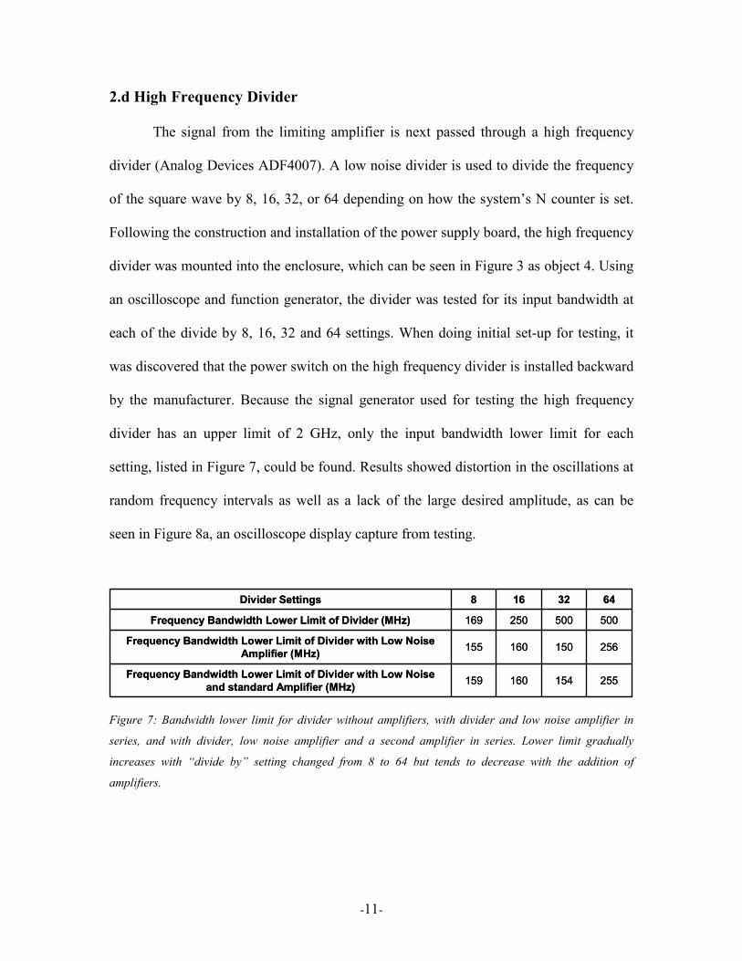
2.d High Frequency Divider
The signal from the limiting amplifier is next passed through a high frequency
divider (Analog Devices ADF4007). A low noise divider is used to divide the frequency
of the square wave by 8, 16, 32, or 64 depending on how the system’s N counter is set.
Following the construction and installation of the power supply board, the high frequency
divider was mounted into the enclosure, which can be seen in Figure 3 as object 4. Using
an oscilloscope and function generator, the divider was tested for its input bandwidth at
each of the divide by 8, 16, 32 and 64 settings. When doing initial set-up for testing, it
was discovered that the power switch on the high frequency divider is installed backward
by the manufacturer. Because the signal generator used for testing the high frequency
divider has an upper limit of 2 GHz, only the input bandwidth lower limit for each
setting, listed in Figure 7, could be found. Results showed distortion in the oscillations at
random frequency intervals as well as a lack of the large desired amplitude, as can be
seen in Figure 8a, an oscilloscope display capture from testing.
Figure 7: Bandwidth lower limit for divider without amplifiers, with divider and low noise amplifier in
series, and with divider, low noise amplifier and a second amplifier in series. Lower limit gradually
increases with “divide by” setting changed from 8 to 64 but tends to decrease with the addition of
amplifiers.
255154160159Frequency Bandwidth Lower Limit of Divider with Low Noise
and standard Amplifier (MHz)
256150160155Frequency Bandwidth Lower Limit of Divider with Low Noise Amplifier (MHz)
500500250169Frequency Bandwidth Lower Limit of Divider (MHz)
6432168Divider Settings
255154160159Frequency Bandwidth Lower Limit of Divider with Low Noise
and standard Amplifier (MHz)
256150160155Frequency Bandwidth Lower Limit of Divider with Low Noise Amplifier (MHz)
500500250169Frequency Bandwidth Lower Limit of Divider (MHz)
6432168Divider Settings

-12-
Figure 8: a) Oscilloscope display capture from testing divider alone at frequency of 800MHz with
+4.5dBm input signal power and divide by 32 setting on high frequency divider. Shows distortion in the
oscillations as well as a lack of the large amplitude desired. b) Oscilloscope display capture from testing
divider with low noise amplifier at frequency of 800MHz with +4.5dBm input signal power and divide by
32 setting on high frequency divider. Shows fixed distortion in oscillations and some enlargement of
amplitude.
2.e Amplifiers and Bias T
To decrease distortion in the signal as well as increase the amplitude of
oscillation, the divided signal then travels through a low noise amplifier (Mini-Circuits
ZFL-500LN), as can be seen in Figure 3 as object 5. Again using an oscilloscope and
signal generator, the low noise amplifier was tested for its bandwidth at each of the divide
by 8, 16, 32 and 64 settings. As before, only the bandwidth lower limit could be found, as
seen in Figure 7. The output signal was between ~5x and ~20x the size of the input
signal coming from the divider and shows significantly less distortion, as is seen in
Figure 8b.
Because adding one amplifier worked so well, the next step was to add a second
amplifier (Mini-Circuits ZFL-500) following the low noise amplifier in series to amplify
the signal sufficiently for use with the Field-Programmable Gate Array (FPGA). The
first amplifier’s low noise characteristic limits its ability to amplify the signal. The
second amplifier may have associated noise, but it produces a robust signal that is well
Time (20 ns/div)
Volts (10 mV/ div)
Volts (100 mV/ div)
Time (20 ns/div)
a) b)

-13-
matched with the voltage levels at the FPGA. Using an oscilloscope and function
generator, the second amplifier was tested for its lower bandwidth limit at each of the
divide by 8, 16, 32, and 64 settings, as seen in Figure 7.
The output signal from the second amplifier is likely to oscillate around zero. For
the FPGA to properly detect the signal, the oscillations must all be positive. In the case
that the output signal from the second amplifier does oscillate around zero, a Bias T will
be installed after the second amplifier to shift the signal into the positive region for
further analysis.
2.f FPGA and 50MHz Digital Clock
From the second amplifier, the signal goes to an FPGA-based digital counter,
which will be installed in the enclosure in the space denoted with a 7 in Figure 3. A
Terasic DE0 development board is equipped with an Altera Cyclone III EP3C16F484
FPGA that is programmed (Verilog) to compare a beat note frequency counter with a
control counter using a 50MHz internal digital clock as a controlled timer. As the clock
runs, it counts the specific number of oscillations expected if the two lasers are locked to
a beat note ∆ω during an allotted amount of time.
When determining what this number would be for this OFLL, length of count
time and accuracy had to be balanced. The longer the count time, the more accurate the
loop filter would be, but it would also take so long it would be inefficient at correcting
transients. Taking these two factors into account and assuming an input signal of ~7 GHz
using the high frequency divider’s divide-by-64 function, a target error signal of 1 MHz
or less was chosen. The ratio between the input signal and error signal was taken to
determine that the “stop count” number should be ~104 or higher, more specifically a

-14-
number of 214 or higher, as a lower “stop count” number would increase the error. The
period would be 20ns for a 50 MHz clock, which, when multiplied by the “stop count”
number 214, translates to a count time of ~328µs. Because this is not a very long count
time, it was decided to increase the value by adding an extra bit to the binary count
number to account for error. This produced a “stop count” number of 216-1 with a
corresponding count time of ~1.3ms to the increase efficiency of correcting transients.
Figure 9: Basic schematic for FPGA program written in Verilog to count beat note frequency and time it
relative to a reference frequency provided by an internal 50 MHz Clock. The difference between the beat
note frequency and an inputted count target number is the output error signal.
Each time the reference counter reaches 216, it is triggered to stop counting and to
make the control counter stop counting as well. Both counters reset to zero to begin
counting again and the beat note counter total is compared to a count target number. The
count target number will be set to expect a specific number of oscillations per unit time.
If more oscillations are incident on the beat note counter than the reference counter in the
allotted time, the frequency is too high. If fewer oscillations are incident on the beat note
Beat Note Counter
Reference Counter
“stop count”number
50 MHz ClockCount Target Number
Beat Note Frequency
stop count (reset)
reset to zero
A
BA-B
A-B
beat note count total
Digital error signal is α ∆ω−reference frequency

-15-
counter than the reference counter in the allotted time, the frequency is too low. This
process will ultimately output the difference between the count target number and the
beat note counter total as the error signal. This basic set-up can be seen in Figure 9 (see
Appendix for full source code).
2.g DAC and Feedback Controller
The digital error signal from the FPGA must be converted back to an analog
signal using a Digital-to-Analog Converter (DAC). This analog error signal is sent to the
Proportional-Integral-Derivative (PID) feedback controller. This is where the signal will
be stabilized and fine tuned to be transmitted to the slave laser. The signal will continue
to travel this optical frequency-locked-loop (OFLL) and be corrected until ∆ω, the beat
note, is constant [1]. The DAC and PID feedback controller will be installed into the
aluminum enclosure in the area marked 8 in Figure 3. Once these pieces have been
constructed and installed, the remainder of the construction process will consist of fine
tuning the system for optimal performance.
3 Conclusions While the College of William and Mary’s Ultra-cold AMO physics laboratory
already has an analog laser lock system, the digital laser lock system has some
advantages. Analog devices tend to work more quickly and with a lower noise level than
digital devices; however the output range of analog phase frequency difference detector is
limited. A digital system allows the user to tailor the gain of the feedback over a wide
range of feedback rates whereas the feedback of an analog lock system is fixed [7].

-16-
Because this design for a digital laser lock system is a combination of analog and digital
systems, the circuit will work more quickly while producing less noise than would an all-
digital system.
While this digital laser offset lock system has many components, the majority of
the loop filter’s work is done within the FPGA. The core program presently in use is
relatively basic. When this system is next upgraded, a feature may be added such that
when a count target number is provided in binary through setting external switches high
and low, that number will be inserted into the core FPGA program. Another option
would be adding a target count number calculator that will compute and update the
desired target count number based on information provided through external switches and
the first iteration of the loop filter. Adding multiple loop filters with different count times
to the core code would be an upgrade that would make the system more accurate as it
would accommodate the benefits of both the increased accuracy of longer count times
and the efficiency of shorter count times.
The ROSA and its associated circuit have been assembled by Megan Ivory,
however its functionality must still be tested. Once the ROSA is confirmed to work, it
will be installed in the aluminum enclosure in the area marked with a 2 in Figure 3. The
DAC and PID feedback controller need to be assembled and installed along with the
FPGA, which has already been tested independently. Testing of the fully assembled
system will determine if a Bias T is necessary. The laser lock will then be applied to the
unstable titanium-sapphire laser or an unlocked diode laser with a stable diode master
laser as a control in the Ultra-cold AMO laboratory.

Appendix Listing 1: Quartus code for FPGA counter used to stabilize slave laser relative to master laser.
///////////////////////////////////////////////////////////////////////////////// // Fix the electronic beat note between 50MHz clock and input electronic signal. // Last modified by Lauren Snowden White 7 May 2012. ///////////////////////////////////////////////////////////////////////////////// module counter101(input1,input2,output1,output1_display); input input1; // reference clock input to reference counter
// 50 MHz internal clock input input2; // beat note frequency input to beat note counter output output1; // reference clock output; used for coding output [15:0] output1_display; // beat note counter output, 16 bits binary reg [15:0] counttime_test_in;
// beat note input counter, gives number of counts/1.3ms, 16 bits binary reg [15:0] counttime_test_out; // beat note output counter, 16 bits binary
// gives number of counts/1.3ms counted by counttime_test_in reg [15:0] counttime_ref;
// reference clock counter gives number of counts/1.3ms, 16 bits binary reg ref_count_complete; // reference clock counter has completed count to 1.3ms, 1 bit binary
// (2^(16)-1 = 65,535 oscillations) initial begin counttime_test_in = 16'b0000000000000000;
// set beat note clock input counter to zero counttime_test_out = 16'b0000000000000000;
// set beat note clock output counter to zero counttime_ref = 16' b0000000000000000;
// set reference 50 MHz clock count time to zero ref_count_complete = 1'b0;
// indicate that reference clock counter should count normally end assign output1_display [15:0] = counttime_test_out [15:0];
// attach so beat note count total is sent to output display always@ (posedge input1) // begin at low to high transition of 50 MHz clock begin counttime_ref <= counttime_ref + 16'b0000000000000001;
// counting of reference 50 MHz clock begins ref_count_complete = 1'b0;
// reference clock counter set low so will count normally if (counttime_ref == 16'b1111111111111111)
// “stop count” # =65,535 beats of reference clock = 1111111111111111 begin counttime_test_out <= counttime_test_in;
// counttime_test_out gives the number of counts counted by // counttime_test_in in 1.3ms
counttime_ref <= 16'b0000000000000000; // reset reference count time to zero
ref_count_complete <= 1'b1; // set high to indicate temp counter is full
end end
-17-

always@ (posedge input2 or posedge ref_count_complete) // begin at low to high transition of beat note signal // or begin at low to high transition of complete reference count indicator
begin if (ref_count_complete == 1'b1) // if reference counter flag high begin counttime_test_in <= 16'b0000000000000000;
// reset input beat note counter to zero end else begin counttime_test_in <= counttime_test_in + 16'b0000000000000001; // begin counting of beat note again end end endmodule
-18-

-19-
Acknowledgements
I would like to thank Professor Aubin for his direction and dedicated support on this
project. I would also like to thank Megan Ivory, Austin Ziltz, and Alexander (Sandro)
Gvakharia for any and all suggestions and assistance given to me on this project.
References
[1] J. Appel, A. MacRae, and A.I. Lvovsky, Meas. Sci. Technol. 20, 055302 (5pp)
(2009); (10.1088/0957-0233/20/5/055302). [2] U. Ernst, A. Marte, F. Schreck, J. Schuster, and G. Rempe, Europhysics Letters
41 (1), pp. 1-6 (1998). [3] K.-K. Ni, S. Ospelkaus, M. H. G. de Miranda, A. Pe’er, B. Neyenhuis, J. J. Zirbel,
S. Kotochigova, P. S. Julienne, D. S. Jin, and J. Ye, Science 322, 231 (2008); published online 18 September 2008 (10.1126/science.1163861).
[4] L. V. Hau, S. E. Harris, Z. Dutton, and C. H. Behroozi, Nature 397, 594-598
(1998); published online 18 February 1999 (10.1038/17561). [5] R. C. Pooser, A. M. Marino, V. Boyer, K. M. Jones, and P. D. Lett, 2009,
Quantum correlated light beams from nondegenerate four-wave mixing in an atomic vapor: the D1 and D2 lines of 85Rb and 87Rb, Optical Society of America.
[6] A. M. Marino and C. R. Stroud, Jr., Rev. Sci. Instrum. 79, 013104 (2007);
published online 11 January 2008 (10.1063/1.2823330). [7] L. Cacciapuoti, M. de Angelis, M. Fattori, G. Lamporesi, T. Petelski, M.
Prevedelli, J. Stuhler, and G. M. Tino, Rev. Sci. Instrum. 76, 053111 (2005); published online 2 May 2005 (10.1063/1.1914785).
[8] R. Getz and B. Moeckel, 1996, Understanding and Eliminating EMI in
Microcontroller Applications, National Semiconductor Corporation, p.13.


![[Chinh Duc Print] Digital-Offset-Printing Brochure](https://img.pdfslide.us/doc/110x75/579054701a28ab900c909865/chinh-duc-print-digital-offset-printing-brochure.jpg)


