Embed Size (px)
Citation preview

WISMO Quik Q26 series
Development Kit Q2686 and Q2687User Guide
Revision: 003Date: February 2006

confidential © Page : 1 / 64 This document is the sole and exclusive property of WAVECOM. Not to be distributed or divulged without prior written agreement.
Ce document est la propriété exlcusive de WAVECOM. Il ne peut être communiqué ou divulgué à des tiers sans son autorisation préalable.
Quik Q26 Series
Development Kit Q2686 and Q2687 User Guide
Reference : WM_BBD_Q26_UGD_001
Revision : 003
Date : 20th February 2006

WM_BBD_Q26_UGD_001-002 20th February 2006
confidential © Page : 2 / 64 This document is the sole and exclusive property of WAVECOM. Not to be distributed or divulged without prior written agreement.
Ce document est la propriété exclusive de WAVECOM. Il ne peut être communiqué ou divulgué à des tiers sans son autorisation préalable.
Document Information
Revision Date History of the evolution 001 24 June 2005 Creation 002 08 Sept 2005 Update for the development kit Q26 version2 003 20 February
2006 Update for the development kit Q26 version3 - Add new § for the parallel bus interface (for Wireless CPU Q2687 only) - New GPIO for CHARGER LED. - New values around the AUDIO1 filters - Measure of current simplified - New schematics

WM_BBD_Q26_UGD_001-002 20th February 2006
confidential © Page : 3 / 64 This document is the sole and exclusive property of WAVECOM. Not to be distributed or divulged without prior written agreement.
Ce document est la propriété exclusive de WAVECOM. Il ne peut être communiqué ou divulgué à des tiers sans son autorisation préalable.
Contents
Document Information......................................................................... 2
Contents.............................................................................................. 3
Table of illustrations............................................................................ 6
Trademarks ......................................................................................... 7
Copyright ............................................................................................ 7
Cautions .............................................................................................. 8
Overview ............................................................................................. 9
Reference documents........................................................................ 10
List of abbreviations.......................................................................... 11
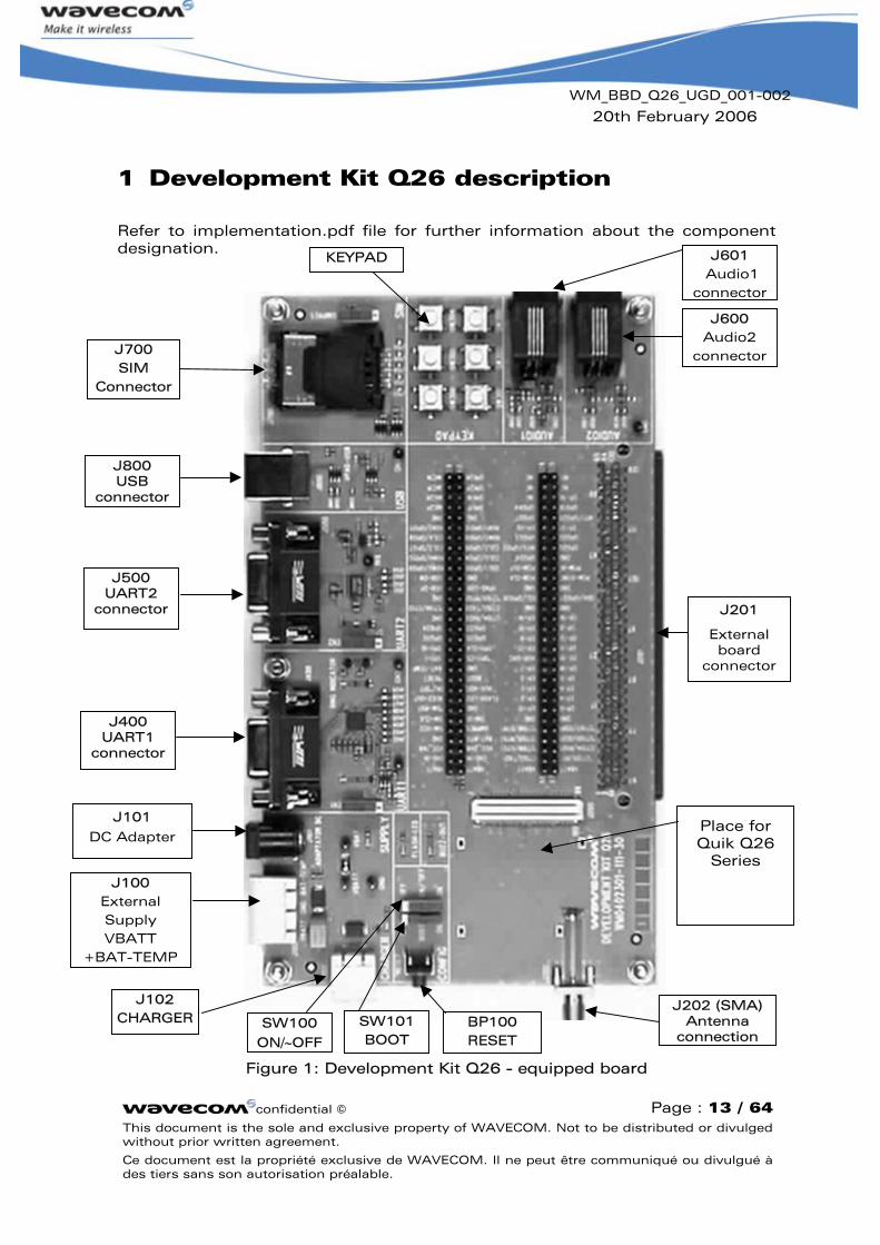
1 Development Kit Q26 description ............................................... 13
2 General description..................................................................... 14 2.1 Development Kit Q26 ............................................................................14 2.2 Special solder ........................................................................................15 2.3 RoHS compliance ..................................................................................15
3 External board connector (J201) description.............................. 16 3.1 Q2686 and Q2687 Wireless CPU signals...............................................16 3.2 External board connector (J201) ...........................................................16
4 Power supply .............................................................................. 22 4.1 LED signalization (“VBAT”)....................................................................22 4.2 External supply......................................................................................23
4.2.1 BAT-TEMP ........................................................................................24 4.3 Main supply adapter .............................................................................24
5 Charger supply & LED ................................................................. 25 5.1 Charger supply......................................................................................25 5.2 LED signalization (“CHARGER”).............................................................26
6 Flash LED (“FLASH-LED”) ............................................................ 27
7 Buzzer LED (“BUZZ-OUT”)........................................................... 27

WM_BBD_Q26_UGD_001-002 20th February 2006
confidential © Page : 4 / 64 This document is the sole and exclusive property of WAVECOM. Not to be distributed or divulged without prior written agreement.
Ce document est la propriété exclusive de WAVECOM. Il ne peut être communiqué ou divulgué à des tiers sans son autorisation préalable.
8 Control functions........................................................................ 28 8.1 ON/~OFF ...............................................................................................28 8.2 ~RESET.................................................................................................28 8.3 BOOT ....................................................................................................28
9 Keypad function.......................................................................... 29
10 UART1 function ........................................................................ 30 10.1 UART1 connector (J400) .......................................................................30 10.2 Configuration of the UART1...................................................................31 10.3 Enable UART1 (“EN1/GPIO19”)..............................................................32 10.4 LED signalization ...................................................................................32
10.4.1 LED “RING INDICATOR” ....................................................32 10.4.2 LED “EN1” .........................................................................32
11 UART2 function ........................................................................ 33 11.1 UART2 connector (J500) .......................................................................33 11.2 Configuration of the UART2...................................................................34 11.3 Enable UART2 (“EN2/GPIO1”)................................................................34 11.4 LED signalization (“EN2”) ......................................................................35
12 SIM function............................................................................. 36 12.1 SIM connector (J700)............................................................................36
13 USB function ............................................................................ 38 13.1 USB connector (J800) ...........................................................................38 13.2 LED signalization (“VPAD-USB”)............................................................39
14 AUDIO functions....................................................................... 40 14.1 AUDIO1 connector (J601)......................................................................40 14.2 AUDIO2 connector (J600)......................................................................41 14.3 Audio functions description...................................................................41
15 Parallel bus interface (with the Q2687 Wireless CPU only) ....... 43 15.1 Parallel bus configurations (with the Q2687 Wireless CPU only) ...........44
16 Antenna function...................................................................... 45 16.1 RF connectors (P200+J202) ..................................................................45
17 ESD functions........................................................................... 46
18 Measures of current ................................................................. 47

WM_BBD_Q26_UGD_001-002 20th February 2006
confidential © Page : 5 / 64 This document is the sole and exclusive property of WAVECOM. Not to be distributed or divulged without prior written agreement.
Ce document est la propriété exclusive de WAVECOM. Il ne peut être communiqué ou divulgué à des tiers sans son autorisation préalable.
19 Starting procedure ................................................................... 49 19.1 Unpacking the Development Kit Q2686 or Q2687 components .............49 19.2 Setting the accessories..........................................................................50 19.3 Power supply ........................................................................................52 19.4 Communication test ..............................................................................52
20 APPENDIXES............................................................................. 53

WM_BBD_Q26_UGD_001-002 20th February 2006
confidential © Page : 6 / 64 This document is the sole and exclusive property of WAVECOM. Not to be distributed or divulged without prior written agreement.
Ce document est la propriété exclusive de WAVECOM. Il ne peut être communiqué ou divulgué à des tiers sans son autorisation préalable.
Table of illustrations
Figure 1: Development Kit Q26 - equipped board ........................................... 13 Figure 2: Power supply voltage (J101 and J102) ........................................... 22 Figure 3: Zoom on “J103”.............................................................................. 22 Figure 4: Power supply voltage ...................................................................... 23 Figure 5: Main supply adapter........................................................................ 24 Figure 6: Charger supply ................................................................................ 25 Figure 7: Switches configuration.................................................................... 28 Figure 8: Keypad configuration....................................................................... 29 Figure 9: UART1 connector ............................................................................ 30 Figure 10: RS232 main serial link ................................................................... 31 Figure 11: Enable UART2 configuration.......................................................... 33 Figure 12: RS232 auxiliary serial link.............................................................. 34 Figure 13: SIM connector ............................................................................... 36 Figure 14: Schematic of switch “SIMPRES” ................................................... 37 Figure 15: USB connector .............................................................................. 38 Figure 16: USB electrical diagram................................................................... 39 Figure 17: AUDIO1 connectorJ601 is a RJ9 4-pin connector.......................... 40 Figure 18: AUDIO2 connector......................................................................... 41 Figure 19: RF connectors ............................................................................... 45 Figure 20: Configuration for the measure of current ....................................... 48

WM_BBD_Q26_UGD_001-002 20th February 2006
confidential © Page : 7 / 64 This document is the sole and exclusive property of WAVECOM. Not to be distributed or divulged without prior written agreement.
Ce document est la propriété exclusive de WAVECOM. Il ne peut être communiqué ou divulgué à des tiers sans son autorisation préalable.
Trademarks
®, WAVECOM®, WISMO®, Open AT® and certain other trademarks and logos appearing on this document, are filed or registered trademarks of Wavecom S.A. in France or in other countries. All other company and/or product names mentioned may be filed or registered trademarks of their respective owners.
Copyright
This manual is copyrighted by WAVECOM with all rights reserved. No part of this manual may be reproduced in any form without the prior written permission of WAVECOM.
WM_BBD_Q26_UGD_001-002 20th February 2006
confidential © Page : 8 / 64 This document is the sole and exclusive property of WAVECOM. Not to be distributed or divulged without prior written agreement.
Ce document est la propriété exclusive de WAVECOM. Il ne peut être communiqué ou divulgué à des tiers sans son autorisation préalable.
Cautions
This Development Kit Q26 series integers 2 kind of Wireless CPU transmitter. These device is to be used only for mobile and fixed applications.
There are the Q2686 and Q2687 Wireless CPU, and they are pin to pin compatible:
Q2686 Wireless CPU is a hardware GSM/GPRS class 10 capable.
Q2687 Wireless CPU is a hardware GSM/GPRS class 12 and EDGE/GPRS class 10 capable.
The antenna(s) used for this transmitter must be installed to provide a separation distance of at least 20 cm from all persons and must not be co-located or operating in conjunction with any other antenna or transmitter. The antenna(s) used for this transmitter must not exceed a gain of 3 dBi for mobile operation and 7 dBi for fixed operation.
Users and OEM integrators must be provided with antenna installation instructions and transmitter operating conditions for satisfying RF exposure compliance. OEM must also be provided with labeling instructions.
These devices contain EGSM/GPRS and EDGE functions (EDGE functions, only for Q2687 Wireless CPU) that are not operational in U.S. territories. This filing is applicable for GSM850 MHz, E-GSM900 MHz, DCS1800 MHz and PCS1900 MHz operations.
Information provided herein by Wavecom is accurate and reliable. However no responsibility is assumed for its use.
General information about Wavecom and its range of products is available at the following internet address: http://www.wavecom.com
No patent liability is assumed with respect to the use of the information contained herein.

WM_BBD_Q26_UGD_001-002 20th February 2006
confidential © Page : 9 / 64 This document is the sole and exclusive property of WAVECOM. Not to be distributed or divulged without prior written agreement.
Ce document est la propriété exclusive de WAVECOM. Il ne peut être communiqué ou divulgué à des tiers sans son autorisation préalable.
Overview
This document is a description of the Development Kit for Quik Q26 Series wireless CPU based on a mother board V3 Ref. WM0402301-111-30.
This Development Kit is an equipment which can be used to start software and hardware development based on Q2686 and Q2687 Wireless CPU.
Refer to the documentation of the Q2686 and Q2687 Wireless CPU for further information.

WM_BBD_Q26_UGD_001-002 20th February 2006
confidential © Page : 10 / 64 This document is the sole and exclusive property of WAVECOM. Not to be distributed or divulged without prior written agreement.
Ce document est la propriété exclusive de WAVECOM. Il ne peut être communiqué ou divulgué à des tiers sans son autorisation préalable.
Reference documents
[1] MOTHER BOARD Development Kit Schematics and PCB, Release 3.0 Ref.: WM0402301-110-30.
[2] WISMO Quik Q2686 Product Technical Specification Ref.: WM_PRJ_Q2686_PTS_001
[3] WISMO Quik Q2686 Customer Design Guideline Ref.: WM_PRJ_Q2686_PTS_003
[4] Title AT Commands Interface Guide for revision X60. Reference: WM_DEV_OAT_UGD_003.
[5] WISMO Quik Q2687 Product Technical Specification Ref.: WA_PRJ_Q2687_PTS_001
[6] WISMO Quik Q2687 Customer Design Guideline Ref.: WA_PRJ_Q2687_PTS_003
[7] Title AT Commands Interface Guide for revision X61. Reference: WM_DEV_OAT_UGD_014.

WM_BBD_Q26_UGD_001-002 20th February 2006
confidential © Page : 11 / 64 This document is the sole and exclusive property of WAVECOM. Not to be distributed or divulged without prior written agreement.
Ce document est la propriété exclusive de WAVECOM. Il ne peut être communiqué ou divulgué à des tiers sans son autorisation préalable.
List of abbreviations
ADC Analog to Digital Converter
AUX AUXiliary
CLK CLocK
CPU Central Process Unit
CTS Clear To Send
DAI Digital Audio Interface
DC Direct Current
DCD Data Carrier Detect
DCE Data Communication Equipment
DSR Data Set Ready
DTE Data Terminal Equipment
DTR Data Terminal Ready
ESD ElectroStatic Discharges
GND GrouND
GPI General Purpose Input
GPIO General Purpose Input Output
GPO General Purpose Output
I/O Input / Output
MIC MICrophone
PC Personal Computer
PCB Printed Circuit Board.
PCM Pulse Code Modulation
PWM Pulse Width Modulation
RF Radio Frequency
RI Ring Indicator
RTC Real Time Clock
RTS Request To Send
RXD Receive Data
SCI Smart Card Interface
SIM Subscriber Identity Module
SPI Serial Peripheral Interface
SPK SPeaKer

WM_BBD_Q26_UGD_001-002 20th February 2006
confidential © Page : 12 / 64 This document is the sole and exclusive property of WAVECOM. Not to be distributed or divulged without prior written agreement.
Ce document est la propriété exclusive de WAVECOM. Il ne peut être communiqué ou divulgué à des tiers sans son autorisation préalable.
TP Test Point
TXD Transmit Data
USB Universal Serial Bus
WM_BBD_Q26_UGD_001-002 20th February 2006
confidential © Page : 1This document is the sole and exclusive property of WAVECOM. Not to be distributed orwithout prior written agreement.
Ce document est la propriété exclusive de WAVECOM. Il ne peut être communiqué ou ddes tiers sans son autorisation préalable.
1 Development Kit Q26 description
Refer to implementation.pdf file for further information about the component designation.
Figure 1: Development Kit Q26 - equipped board
J101
DC Adapter
Acon
Aco
J700 SIM
Connector
J100 External Supply VBATT
+BAT-TEMP
BP100 RESET
SW101 BOOT O
J
con
PQu
KEYPAD
E
c
J500 UART2
connector
J400 UART1
connector
J102 CHARGER
J601 udio1
nnector
J600 udio2 nector
lace for ik Q26
Series
J201
xternal board
onnector
SW100 N/∼OFF
800 USB nector
J202 (SMA) Antenna
connection
3 / 64 divulged
ivulgué à

WM_BBD_Q26_UGD_001-002 20th February 2006
confidential © Page : 14 / 64 This document is the sole and exclusive property of WAVECOM. Not to be distributed or divulged without prior written agreement.
Ce document est la propriété exclusive de WAVECOM. Il ne peut être communiqué ou divulgué à des tiers sans son autorisation préalable.
2 General description
2.1 Development Kit Q26
All functions of the Development Kit Q26 are provided by the Q2686 or Q2687 Wireless CPU.
Interfaces on board:
- 1 external board to board connector and TP to access all signals of the Wireless CPU.
- Parallel bus (only for the Q2687 Wireless CPU)
- Main serial link RS232, UART1(*) with full signals
- Ring Indicator
- Auxiliary serial link RS232, UART2* with 4 signals
- Slave USB*, compliant USB 2.0.
- SIM* 1.8/3v with gestion of Sim presence
- 6-button Keypad
- 2 AUDIO* connectors (AUDIO 1, AUDIO 2)
- LEDs for several indications
- RESET Pushbutton
- Power supply connectors
- ON/OFF switch
- BOOT switch
- Buzzer LED
- Flash LED
- Charger LED
(*) The particularity of the Development Kit Q26 it is that each signals peripheral can be electrically removed independently via special solder. (refer to § 2.2).

WM_BBD_Q26_UGD_001-002 20th February 2006
confidential © Page : 15 / 64 This document is the sole and exclusive property of WAVECOM. Not to be distributed or divulged without prior written agreement.
Ce document est la propriété exclusive de WAVECOM. Il ne peut être communiqué ou divulgué à des tiers sans son autorisation préalable.
2.2 Special solder
The PCB print is used for the peripherals that are electrically removable.
To connect signals between the Quik Q26 series and the dedicated connector on the Development Kit Q26, solder these PCB print.
To connect signals between the Quik Q26 series and the external board connector (J201) it is recommended not to solder these PCB print. (i.e. prototyped a daughter board)
These interfaces are electrically removable via the “special solder”:
- UART1 (from J402 to J409)
- UART2 (from J501 to J504)
- AUDIO1 (from J602 to J605)
- AUDIO2 (from J606 to J609)
- SIM (from J701 to J705)
- USB (from J801 to J803,signals plus power)
- Power supply of Development Kit (from J103, all components except the Wireless CPU).
2.3 RoHS compliance
The Quik Q26 Series and the Development Kit Q26 board are now compliant with RoHS (Restriction of Hazardous Substances in Electrical and Electronic Equipment) Directive 2002/95/EC which sets limits for the use of certain restricted hazardous substances. This directive states that “from 1st July 2006, new electrical and electronic equipment put on the market does not contain lead, mercury, cadmium, hexavalent chromium, polybrominated biphenyls (PBB) or polybrominated diphenyl ethers (PBDE)”.
Wireless CPUs which are compliant with this directive are identified by the RoHS logo on their label.

WM_BBD_Q26_UGD_001-002 20th February 2006
confidential © Page : 16 / 64 This document is the sole and exclusive property of WAVECOM. Not to be distributed or divulged without prior written agreement.
Ce document est la propriété exclusive de WAVECOM. Il ne peut être communiqué ou divulgué à des tiers sans son autorisation préalable.
3 External board connector (J201) description
3.1 Q2686 and Q2687 Wireless CPU signals
All signals of the Q2686 and Q2687 Wireless CPU are connected to the external board connector (J201). and are available via TP on the center of Development Kit Q26. The pinout of J201 connector are listing below.
For further information about the Quik Q2686 Wireless CPU signals and multiplexing, refer to [2].
For further information about the Quik Q2687 Wireless CPU signals and multiplexing, refer to [5].
3.2 External board connector (J201)
Pin # Name I/O(*) I/O type Description
1 VBATT I Supply Battery Input
2 VBATT I Supply Battery Input
3 CHG-IN I Supply Current source input
4 CHG-IN I Supply Current source input
5 VCC_1V8 O Supply 1.8V digital supply output
6 VCC_2V8 O Supply 2.8V digital supply output
7 GND
8 BAT-RTC I/O Supply RTC back-up supply
9 SIM-VCC O Supply SIM card supply
10 SIMPRES/
GPIO18
I 1V8 SIM card detect
11 SIM-CLK O 1V8 / 2V9 SIM clock
12 SIM-IO I/O 1V8 / 2V9 SIM data
13 ~SIM-RST O 1V8 / 2V9 SIM reset
14 GND
15 BUZZ-OUT O Open drain PWM / Buzzer output
16 FLASH-LED O Open Drain Charging indicator
17 ON/ ~OFF I VBATT Wireless CPU Power ON
18 AUX-ADC I Analog Auxiliary ADC
19 ~RESET I/O 1V8 Wireless CPU Reset
20 BOOT I 1V8 SW download (with a Wavecom software “DWLwin”)

WM_BBD_Q26_UGD_001-002 20th February 2006
confidential © Page : 17 / 64 This document is the sole and exclusive property of WAVECOM. Not to be distributed or divulged without prior written agreement.
Ce document est la propriété exclusive de WAVECOM. Il ne peut être communiqué ou divulgué à des tiers sans son autorisation préalable.
Pin # Name I/O(*) I/O type Description 21 BAT-TEMP I Analog ADC input for battery temperature
measurement
22 GND
23 SPI1-I / GPIO30
I 2V8 SPI1 Serial input
(Multiplexed)
24 ~SPI1-CS / GPIO31
O 2V8 SPI1 Enable
(Multiplexed)
25 SPI1-IO / GPIO29
I/O 2V8 SPI1 Serial input/output (Multiplexed)
26 SPI1-CLK / GPIO28
O 2V8 SPI1 Serial Clock
(Multiplexed)
27 SPI2-CLK / GPIO32
O 2V8 SPI2 Serial Clock
(Multiplexed)
28 SPI2-CS / GPIO35
O 2V8 SPI2 Enable
(Multiplexed)
29 SPI2-I / GPIO34
I 2V8 SPI2 Serial input
(Multiplexed)
30 SPI2-IO / GPIO33
I/O 2V8 SPI2 Serial input/output (Multiplexed)
31 GND
32 CT104-RXD2 / GPIO15
O 1V8 Auxiliary RS232
Receive Serial Data
(According to PC view and Multiplexed)
33 ~CT106-CTS2 / GPIO16
O 1V8 Auxiliary RS232
Clear To Send
(According to PC view and Multiplexed)
34 CT103-TXD2 / GPIO14
I 1V8 Auxiliary RS232
Transmit Serial Data
(According to PC view and Multiplexed)
35 GND
36 ~CT105-RTS2 / GPIO17
I 1V8 Auxiliary RS232 Request To Send
(According to PC view and Multiplexed)
37 USB-DP I/O 3V3 Differential data interface positive
38 VPAD-USB I 3V3 USB power supply
39 USB-DM I/O 3V3 Differential data interface negative
40 GND

WM_BBD_Q26_UGD_001-002 20th February 2006
confidential © Page : 18 / 64 This document is the sole and exclusive property of WAVECOM. Not to be distributed or divulged without prior written agreement.
Ce document est la propriété exclusive de WAVECOM. Il ne peut être communiqué ou divulgué à des tiers sans son autorisation préalable.
Pin # Name I/O(*) I/O type Description
41 ROW0 / GPIO9
I/O 1V8 Row scan (Multiplexed)
42 COL1 / GPIO5 I/O 1V8 Column scan (Multiplexed)
43 ROW4 / GPIO13
I/O 1V8 Row scan (Multiplexed)
44 COL0 / GPIO4 I/O 1V8 Column scan (Multiplexed)
45 COL3 / GPIO7 I/O 1V8 Column scan (Multiplexed)
46 COL2 / GPIO6 I/O 1V8 Column scan (Multiplexed)
47 COL4 / GPIO8 I/O 1V8 Column scan (Multiplexed)
48 ROW3 / GPIO12
I/O 1V8 Row scan (Multiplexed)
49 ROW2 / GPIO11
I/O 1V8 Row scan (Multiplexed)
50 ROW1 / GPIO10
I/O 1V8 Row scan (Multiplexed)
51 GND
52 GND
53 MIC2P I Analog Microphone 2 positive input
54 SPK1P O Analog Speaker 1 positive output
55 MIC2N I Analog Microphone 2 negative input
56 SPK1N O Analog Speaker 1 negative output
57 MIC1P I Analog Microphone 1 positive input
58 SPK2P O Analog Speaker 2 positive output
59 MIC1N I Analog Microphone 1 negative input
60 SPK2N O Analog Speaker 2 negative output
61 NC Not connected
62 NC Not connected
63 NC Not connected
64 NC Not connected
65 NC Not connected
66 VBATT I Supply Battery Input
67 VBATT I Supply Battery Input
68 CT103-TXD1 / GPIO36
I 2V8 Main RS232 Transmit Serial Data
(According to PC view and Multiplexed)
69 ~CT125-RI1 / GPIO42
O 2V8 Main RS232 Ring indicator
(According to PC view and Multiplexed)
70 ~CT106-CTS1 / GPIO39
O 2V8 Main RS232 Clear To Send
(According to PC view and Multiplexed)

WM_BBD_Q26_UGD_001-002 20th February 2006
confidential © Page : 19 / 64 This document is the sole and exclusive property of WAVECOM. Not to be distributed or divulged without prior written agreement.
Ce document est la propriété exclusive de WAVECOM. Il ne peut être communiqué ou divulgué à des tiers sans son autorisation préalable.
Pin # Name I/O(*) I/O type Description
71 CT104-RXD1 / GPIO37
O 2V8 Main RS232 Receive Serial Data
(According to PC view and Multiplexed)
72 ~CT105-RTS1 / GPIO38
I 2V8 Main RS232 Request To Send
(According to PC view and Multiplexed)
73 ~CT109-DCD1 / GPIO43
O 2V8 Main RS232 Data Carrier Detect
(According to PC view and Multiplexed)
74 ~CT108-2-DTR1 / GPIO41
I 2V8 Main RS232 Data Terminal Ready
(According to PC view and Multiplexed)
75 ~CT107-DSR1 / GPIO40
O 2V8 Main RS232 Data Set Ready
(According to PC view and Multiplexed)
76 GND
77 GND
78 EP17 (**)Depend of the Quik Q26 series
79 EP0 (**)Depend of the Quik Q26 series
80 EP2 (**)Depend of the Quik Q26 series
81 EP4 (**)Depend of the Quik Q26 series
82 EP1 (**)Depend of the Quik Q26 series
83 EP6 (**)Depend of the Quik Q26 series 84 EP3 (**)Depend of the Quik Q26 series
85 EP5 (**)Depend of the Quik Q26 series
86 EP7 (**)Depend of the Quik Q26 series
87 EP18 (**)Depend of the Quik Q26 series
88 AUX-DAC O 2V2 DAC
89 EP15 (**)Depend of the Quik Q26 series
90 EP13 (**)Depend of the Quik Q26 series
91 EP11 (**)Depend of the Quik Q26 series
92 EP9 (**)Depend of the Quik Q26 series
93 EP12 (**)Depend of the Quik Q26 series
94 EP10 (**)Depend of the Quik Q26 series
95 EP8 (**)Depend of the Quik Q26 series
96 EP14 (**)Depend of the Quik Q26 series
97 EP16 (**)Depend of the Quik Q26 series
98 GND
99 GND

WM_BBD_Q26_UGD_001-002 20th February 2006
confidential © Page : 20 / 64 This document is the sole and exclusive property of WAVECOM. Not to be distributed or divulged without prior written agreement.
Ce document est la propriété exclusive de WAVECOM. Il ne peut être communiqué ou divulgué à des tiers sans son autorisation préalable.
Pin # Name I/O(*) I/O type Description 100 SCL / GPIO26 I/O Open drain Serial Clock / General purpose input-
output
101 SDA / GPIO27
I/O Open drain Serial Data / General purpose input-output
102 GND
103 GND
104 PCM-CLK O 1V8 Data clock
105 PCM-SYNC O 1V8 Frame synchronization 8Khz
106 PCM-OUT O 1V8 Data output
107 PCM-IN I 1V8 Data input
108 GPIO24 I/O 2V8 General purpose input / output
109 GND
110 INT0/ GPIO3 I/O 1V8 Interruption 0 / General purpose input-output
111 GPIO20 I/O 2V8 General purpose input / output
112 GPIO23 I/O 2V8 General purpose input / output
113 GPIO22 I/O 2V8 General purpose input / output
114 EP20 I/O 1V8 (**)Depend of the Quik Q26 series
115 EP21 I/O 1V8 (**)Depend of the Quik Q26 series
116 GPIO21 I/O 2V8 General purpose input / output
117 INT1/ GPIO25
I/O 2V8 Interruption 1 / General purpose input-output
118 GPIO44 I/O 2V8 General purpose input / output
119 GPIO19 I/O 2V8 General purpose input / output
120 NC Not connected
121 EP19 I/O 1V8 (**)Depend of the Quik Q26 series
122 NC Not connected
123 NC Not connected
124 NC Not connected
125 NC Not connected
126 NC Not connected
127 NC Not connected

WM_BBD_Q26_UGD_001-002 20th February 2006
confidential © Page : 21 / 64 This document is the sole and exclusive property of WAVECOM. Not to be distributed or divulged without prior written agreement.
Ce document est la propriété exclusive de WAVECOM. Il ne peut être communiqué ou divulgué à des tiers sans son autorisation préalable.
Pin # Name I/O(*) I/O type Description
128 NC Not connected
129 NC Not connected
130 NC Not connected
Table 1: Pin out of the external board connector (J201)
(*)According to Quik Q26 view.
(**) Refer to Figure 1 and Table 19. .

WM_BBD_Q26_UGD_001-002 20th February 2006
confidential © Page : 22 / 64 This document is the sole and exclusive property of WAVECOM. Not to be distributed or divulged without prior written agreement.
Ce document est la propriété exclusive de WAVECOM. Il ne peut être communiqué ou divulgué à des tiers sans son autorisation préalable.
4 Power supply
There are at choice two power supply for starting the Development Kit Q26:
• DC external supply (via J100).
• AC/DC adapter (via J101).
These power supplies are protected by a transient voltage suppressor.
Figure 2: Power supply voltage (J101 and J102)
Each of these power supply is used for BOTH the Wireless CPU and the peripherals on the Development Kit Q26.
It is possible to dissociate the power supply for the Wireless CPU (“VBATT”, measurable via the TP153) and for the peripherals (“VBAT”, measurable via the TP157).
Figure 3: Zoom on “J103”
A measure of current is possible between the VBATT and VBAT via J103 (refer to § 18).
4.1 LED signalization (“VBAT”)
“VBAT” indicator is a green LED. It signalizes the external power supply presence. In other words, peripherals and Quik Q26 Series are respectively powered via VBAT and VBATT.
So the Development Kit Q26 is operational.

WM_BBD_Q26_UGD_001-002 20th February 2006
confidential © Page : 23 / 64 This document is the sole and exclusive property of WAVECOM. Not to be distributed or divulged without prior written agreement.
Ce document est la propriété exclusive de WAVECOM. Il ne peut être communiqué ou divulgué à des tiers sans son autorisation préalable.
LED VBATT VBAT
Light ON ON ON
Light OFF Can be ON*
OFF
Table 2: LED of “VBAT”
* If the special solder, J103, is not soldered and external power supply is plugged in.
4.2 External supply
The J100 connector has three contacts:
J100:1-2: for the power supply.
J100:2-3: refer to § 4.2.1.
13 2
GND VBATTBAT-TEMP
Figure 4: Power supply voltage
VMIN VNOM VMAX
VBATT1,2 3.2v 3.6v (*)
(*) Refer to doc[2] or doc [5]
Table 3: Electrical Characteristics
(1) : This value has to be guarantied during the burst (with 2.0A Peak in GSM, GPRS mode)
(2) : Maximum operating Voltage Stationary Wave Ratio (VSWR) is 2:1.

WM_BBD_Q26_UGD_001-002 20th February 2006
confidential © Page : 24 / 64 This document is the sole and exclusive property of WAVECOM. Not to be distributed or divulged without prior written agreement.
Ce document est la propriété exclusive de WAVECOM. Il ne peut être communiqué ou divulgué à des tiers sans son autorisation préalable.
4.2.1 BAT-TEMP
This signal is an input (ADC) in the Wireless CPU.
J100:2-3 also allows simulation of the temperature level from a sensor inside the battery.
VMIN VNOM VMAX
BAT-TEMP 0 - 2v
Table 4: Electrical Characteristics
The divisor bridge with R100, R101 is not finalized (refer to [3] or [6]).
4.3 Main supply adapter
The J101 connector powers the Development Kit Q26 using the AC power supply cable.
Figure 5: Main supply adapter
The only supported reference is:
Manufacturer Reference Characteristics
SINPRO SPU12C-101 4v DC / 2.5 A.
Table 5: Main supply adapter reference

WM_BBD_Q26_UGD_001-002 20th February 2006
confidential © Page : 25 / 64 This document is the sole and exclusive property of WAVECOM. Not to be distributed or divulged without prior written agreement.
Ce document est la propriété exclusive de WAVECOM. Il ne peut être communiqué ou divulgué à des tiers sans son autorisation préalable.
5 Charger supply & LED
5.1 Charger supply
The J102 is used to simulate a charger.
This power supply is protected by a transient voltage suppressor.
When the charger is used, the battery must be connected.
12
GND(-) CHG-IN(+)
Figure 6: Charger supply
VMIN VNOM VMAX
CHG-IN Voltage
(for I=Imax)
4.6(*)v 6v
(*) To be parameterized as per battery manufacturer.
Table 6: Power supply voltage

WM_BBD_Q26_UGD_001-002 20th February 2006
confidential © Page : 26 / 64 This document is the sole and exclusive property of WAVECOM. Not to be distributed or divulged without prior written agreement.
Ce document est la propriété exclusive de WAVECOM. Il ne peut être communiqué ou divulgué à des tiers sans son autorisation préalable.
5.2 LED signalization (“CHARGER”)
The “CHARGER“ LED location is shown in the following figure:
“CHARGER” indicator is a red LED controlled by the GPIO21 provided by the Wireless CPU. This LED represents only the logic level of GPIO21.

WM_BBD_Q26_UGD_001-002 20th February 2006
confidential © Page : 27 / 64 This document is the sole and exclusive property of WAVECOM. Not to be distributed or divulged without prior written agreement.
Ce document est la propriété exclusive de WAVECOM. Il ne peut être communiqué ou divulgué à des tiers sans son autorisation préalable.
6 Flash LED (“FLASH-LED”)
The “FLASH-LED “ location is shown in the following figure:
This LED works in two modes:
• Wireless CPU is in OFF state:
“FLASH-LED” blinks in pre-charging mode (via J102 connector).
• Wireless CPU is in ON state:
“FLASH-LED” indicates the network status.
For more information (refer to [2] or [5]).
7 Buzzer LED (“BUZZ-OUT”)
The “BUZZ-OUT“ LED location is shown in the following figure:
“BUZZ-OUT” indicator is a yellow LED controlled by the signal with the same name provided by the Wireless CPU. It is drove by the PWM signal (open drain).

WM_BBD_Q26_UGD_001-002 20th February 2006
confidential © Page : 28 / 64 This document is the sole and exclusive property of WAVECOM. Not to be distributed or divulged without prior written agreement.
Ce document est la propriété exclusive de WAVECOM. Il ne peut être communiqué ou divulgué à des tiers sans son autorisation préalable.
8 Control functions
Figure 7: Switches configuration
8.1 ON/~OFF
Once the Development Kit Q26 is supplied by the external source (via J100 or J101), the ON/~OFF switch provides the VBATT to the Wireless CPU when it is “ON”.
After 1 second it can be switch off. (refer to [2] or [5] and[3] or [6]).
8.2 ~RESET
The pushbutton ~RESET starts a general reset when it is pushed.
An Operating System reset is preferred to a HW reset.
8.3 BOOT
The BOOT switch is only used for download new software to the Wireless CPU via UART1 with the Wavecom software “DWLWin”.
It must be on “OFF” position.
Mode BOOT ON/~OFF
Normal OFF ON
Backup download
With „DWLWin“
ON ON
Table 7 : BOOT configuration

WM_BBD_Q26_UGD_001-002 20th February 2006
confidential © Page : 29 / 64 This document is the sole and exclusive property of WAVECOM. Not to be distributed or divulged without prior written agreement.
Ce document est la propriété exclusive de WAVECOM. Il ne peut être communiqué ou divulgué à des tiers sans son autorisation préalable.
9 Keypad function
Only 6 keypads are connected on the Development Kit Q26.
Figure 8: Keypad configuration
The following table shows the matrix of the keyboard:
COL0 COL1 COL2 COL3 COL4
ROW0 SW300 - - - -
ROW1 - SW301 - - -
ROW2 - - SW302 - -
ROW3 - - - SW303 SW304
ROW4 - - - - SW305
Table 8: Matrix of the keyboard
Example: If the key SW300 is pressed, an electric detection will be made on ROW0 and COL0.

WM_BBD_Q26_UGD_001-002 20th February 2006
confidential © Page : 30 / 64 This document is the sole and exclusive property of WAVECOM. Not to be distributed or divulged without prior written agreement.
Ce document est la propriété exclusive de WAVECOM. Il ne peut être communiqué ou divulgué à des tiers sans son autorisation préalable.
10 UART1 function
The UART1 function is the main RS232 serial link of Wireless CPU in 3.0V on the Development Kit Q26.
This function can be electrically detached with special solder not soldered (from J402 to J409).
For example, that allows to transmit undisturbed signals via the external connector (J201).
By default, the UART1 is available on its dedicated connector J400 (J402 to J409 soldered).
10.1 UART1 connector (J400)
12345
6789
Figure 9: UART1 connector
J400 is a SUB-D 9-pin female connector. The Table bellow gives the description of the signals of this connector.
Pin Number
Signal Name
I/O I/O Type Description
1 CT109 DCD
O RS232 (V24/V28)
Data Carrier Detect
2 CT104 RXD
O RS232 (V24/V28)
Receive serial data
3 CT103 TXD
I RS232 (V24/V28)
Transmit serial data
4 CT108-2 DTR
I RS232 (V24/V28)
Data Terminal Ready
5 GND Ground

WM_BBD_Q26_UGD_001-002 20th February 2006
confidential © Page : 31 / 64 This document is the sole and exclusive property of WAVECOM. Not to be distributed or divulged without prior written agreement.
Ce document est la propriété exclusive de WAVECOM. Il ne peut être communiqué ou divulgué à des tiers sans son autorisation préalable.
Pin Number
Signal Name
I/O I/O Type Description
6 CT107 DSR
O RS232 (V24/V28)
Data Set Ready
7 CT105 RTS
I RS232 (V24/V28)
Request To Send
8 CT106 CTS
O RS232 (V24/V28)
Clear To Send
9 CT125 RI
O RS232 (V24/V28)
Ring Indicator
Table 9: Pin out of the UART1 connector
10.2 Configuration of the UART1
The Development Kit Q26 acts as a DCE and is connected to a DTE (PC or terminal) with a “straight cable”.
This is a full UART.
DTE DevelopmentKit Q26
(DCE)
CT103 / TX
CT108-2 / DTR
CT105 / RTS
CT104 / RX
CT106 / CTS
CT107 / DSR
CT109 / DCD
CT125 / RI
Figure 10: RS232 main serial link

WM_BBD_Q26_UGD_001-002 20th February 2006
confidential © Page : 32 / 64 This document is the sole and exclusive property of WAVECOM. Not to be distributed or divulged without prior written agreement.
Ce document est la propriété exclusive de WAVECOM. Il ne peut être communiqué ou divulgué à des tiers sans son autorisation préalable.
10.3 Enable UART1 (“EN1/GPIO19”)
A switch “EN1/GPIO19” can drive the shutdown mode of the RS232 transceiver.
By default the RS232 transceiver is in active mode. (switch to “EN1”). In the other case (switch to “GPIO19”) the GPIO drives the shutdown mode.
Switch “EN1/GPIO19” UART1 LED “EN1”
EN1 ON
(in hardware) LIGHTS
0L ON LIGHTS GPIO19
1L OFF EXTINCT
Table 10: Enable UART1 configuration
10.4 LED signalization
10.4.1 LED “RING INDICATOR”
“RING INDICATOR” indicator is a yellow LED controlled by the ~CT125-RI1/GPIO42 signal provided by the Wireless CPU.
It is possible to activate a « visual » mode with Command AT (AT+WRIM=0, refer to. [4] or [7]). And when there is an incoming call, this signal is low and high all 0.5sec.
So the “RING INDICATOR” LED is blinking.
10.4.2 LED “EN1”
“EN1” indicator is a green LED controlled by the EN1 or GPIO19 signals provided by the Wireless CPU.
LED “EN1” lights when the RS232 transceiver is operational (see configuration in Table 10).

WM_BBD_Q26_UGD_001-002 20th February 2006
confidential © Page : 33 / 64 This document is the sole and exclusive property of WAVECOM. Not to be distributed or divulged without prior written agreement.
Ce document est la propriété exclusive de WAVECOM. Il ne peut être communiqué ou divulgué à des tiers sans son autorisation préalable.
11 UART2 function
The UART2 function is the auxiliary RS232 serial link of the Wireless CPU in 1.8V.
This function can be electrically detached with special solder not soldered (from J501 to J504).
For example, that allows to transmit undisturbed signals via the external connector (J201).
By default, the UART2 is available on its dedicated connector J500 (J501 to J504 soldered).
11.1 UART2 connector (J500)
12345
6789
Figure 11: Enable UART2 configuration
J500 is a SUB-D 9-pin female connector. The Table bellow gives the description of the signals of this connector.
Pin Number Signal Name I/O I/O Type Description
1 Not used(*) - - -
2 CT104 RXD O RS232 (V24/V28)
Receive serial data
3 CT103 TXD I RS232 (V24/V28)
Transmit serial data
4 Not used(*) - - -
5 GND Ground
6 Not used(*) - - -

WM_BBD_Q26_UGD_001-002 20th February 2006
confidential © Page : 34 / 64 This document is the sole and exclusive property of WAVECOM. Not to be distributed or divulged without prior written agreement.
Ce document est la propriété exclusive de WAVECOM. Il ne peut être communiqué ou divulgué à des tiers sans son autorisation préalable.
Pin Number Signal Name I/O I/O Type Description
7 CT105 RTS
I RS232 (V24/V28)
Request To Send
8 CT106CTS O RS232 (V24/V28)
Clear To Send
9 Not used(*) - - -
(*)Only 4 signals are used.
Table 11: Pin out of the UART2 connector
11.2 Configuration of the UART2
The Development Kit Q26 acts as a DCE and is connected to a DTE (PC or terminal) with a “straight cable”.
There are only 4 signals on the UART2.
DTE DevelopmentKit Q26
(DCE)
CT103 / TX
CT105 / RTS
CT104 / RX
CT106 / CTS
Figure 12: RS232 auxiliary serial link
11.3 Enable UART2 (“EN2/GPIO1”)
A switch “EN2/GPIO1” can drive the shutdown mode of the RS232 transceiver.
By default the RS232 transceiver is in active mode. (switch to “EN2”). In the other case (switch to “GPIO1”) the GPIO drives the shutdown mode.
Switch “EN2/GPIO1” UART2 LED “EN2”
EN2 ON (in hardware) LIGHTS
1L ON LIGHTS GPIO1 0L OFF EXTINCT
Table 12: Enable UART2 configuration

WM_BBD_Q26_UGD_001-002 20th February 2006
confidential © Page : 35 / 64 This document is the sole and exclusive property of WAVECOM. Not to be distributed or divulged without prior written agreement.
Ce document est la propriété exclusive de WAVECOM. Il ne peut être communiqué ou divulgué à des tiers sans son autorisation préalable.
11.4 LED signalization (“EN2”)
“EN2” indicator is a green LED controlled by the EN2 or GPIO1 signals provided by the Wireless CPU.
LED “EN2” lights when the RS232 transceiver is operational (see configuration in Table 12).

WM_BBD_Q26_UGD_001-002 20th February 2006
confidential © Page : 36 / 64 This document is the sole and exclusive property of WAVECOM. Not to be distributed or divulged without prior written agreement.
Ce document est la propriété exclusive de WAVECOM. Il ne peut être communiqué ou divulgué à des tiers sans son autorisation préalable.
12 SIM function
12.1 SIM connector (J700)
J700 is a standard 1V8 or 3V SIM socket.
Figure 13: SIM connector
The Table bellow gives the description of the signals of this connector.
Pin Number
Signal Name
I/O I/O Type Description Comment
1 SIM-VCC O 1V8 or 2V9 SIM Power Supply
2 SIM-RST O 1V8 or 2V9 SIM Reset
3 SIM-CLK O 1V8 or 2V9 SIM Clock
4 SIMPRES I 1V8 max.(*) SIM Card Detect Multiplexed with GPIO18
5 GND Ground
6 VPP Not connected
7 SIM_DATA I/O 1V8 or 2V9 SIM Data
8 CC8 1V8 SIMPRES signal supply
(*) For either 1V8 or 3V SIM cards.
Table 13: Pin out of the SIM connector

WM_BBD_Q26_UGD_001-002 20th February 2006
confidential © Page : 37 / 64 This document is the sole and exclusive property of WAVECOM. Not to be distributed or divulged without prior written agreement.
Ce document est la propriété exclusive de WAVECOM. Il ne peut être communiqué ou divulgué à des tiers sans son autorisation préalable.
The SIM interface controls both the 2.9V and 1.8V SIM cards.
ESD protections are used on the 5 SIM signals
This function can be electrically detached with special solder not soldered (from J701 to J705).
For example, that allows to transmit undisturbed signals via the external connector (J201).
By default, the SIM signals are available on its dedicated connector J700 (J701 to J705 soldered).
SIMPRES presents the following options:
If the SIMPRES signal is used by the application (detection of SIM card presence by the SIM socket), the “SIMPRES” switch must move to “SIMPRES” (contact 1-2 used).
Else to simulate all the time the SIM card presence (without the SIM socket) the “SIMPRES” switch must move to other side (contact 2-3 used).
Switch
“SIMPRES”
SIM card presence
SIMPRES Depend of the real SIM presence
Other side Simulate a SIM presence
Table 14: SIMPRES configuration
SIM socket
J700
WISMO Quik Q26
Series
J200
VCC_1V8
SIM-CLK
~SIM-RST
SIM-VCCSIM- IO
SIMPRES
Figure 14: Schematic of switch “SIMPRES”

WM_BBD_Q26_UGD_001-002 20th February 2006
confidential © Page : 38 / 64 This document is the sole and exclusive property of WAVECOM. Not to be distributed or divulged without prior written agreement.
Ce document est la propriété exclusive de WAVECOM. Il ne peut être communiqué ou divulgué à des tiers sans son autorisation préalable.
13 USB function
ESD protections are used on the 2 USB signals.
This function can be electrically removed with special solder not soldered (from J801 to J803).
For example, that allows to transmit undisturbed signals via the external connector (J201).
By default, the USB signals are available on its dedicated connector J800 (J801 to J803 soldered).
13.1 USB connector (J800)
J800 is a USB Series type B receptacle.
12
3 4
Figure 15: USB connector
Pin Number
Signal Name
I/O I/O Type Description
1 VBUS I Power supply + 5 VDC
2 DM I/O Digital USB negative line
3 DP I/O Digital USB positive line
4 GND Power supply Ground
Shell Shielding
Table 15: Pin out of the USB connector

WM_BBD_Q26_UGD_001-002 20th February 2006
confidential © Page : 39 / 64 This document is the sole and exclusive property of WAVECOM. Not to be distributed or divulged without prior written agreement.
Ce document est la propriété exclusive de WAVECOM. Il ne peut être communiqué ou divulgué à des tiers sans son autorisation préalable.
13.2 LED signalization (“VPAD-USB”)
“VPAD-USB” indicator is a green LED controlled by the presence of VBUS (when the plug is in the USB connector).
The power supply for the USB interface in the Wireless CPU is providing from the USB connector.
If a USB cable is plugged the LED light and VPAD-USB (the output of a regulator (LDO)) is to 3.3v.
But the special solder (J803) must be soldered for to power the USB interface in the Wireless CPU. So by default J803 is soldered.
USB socket
J800
WISMO Quik Q26
Series
J200
USB -DM USB - DP
VPAD - USB
VBU S J803
ESD protections
J801 J802
LDO
Figure 16: USB electrical diagram

WM_BBD_Q26_UGD_001-002 20th February 2006
confidential © Page : 40 / 64 This document is the sole and exclusive property of WAVECOM. Not to be distributed or divulged without prior written agreement.
Ce document est la propriété exclusive de WAVECOM. Il ne peut être communiqué ou divulgué à des tiers sans son autorisation préalable.
14 AUDIO functions
There are 2 AUDIO interfaces in the Wireless CPU.
14.1 AUDIO1 connector (J601)
1 2 3 4
Figure 17: AUDIO1 connectorJ601 is a RJ9 4-pin connector.
The Table bellow gives the description of the signals of this connector.
Pin Number
Signal Name
I/O I/O Type Description
1 MIC1N I Analog Auxiliary microphone
negative input
2 SPK1N O Analog Auxiliary speaker negative output
3 SPK1P O Analog Auxiliary speaker positive output
4 MIC1P I Analog Auxiliary microphone
positive input
Table 16: Pin out of the AUDIO1 connector

WM_BBD_Q26_UGD_001-002 20th February 2006
confidential © Page : 41 / 64 This document is the sole and exclusive property of WAVECOM. Not to be distributed or divulged without prior written agreement.
Ce document est la propriété exclusive de WAVECOM. Il ne peut être communiqué ou divulgué à des tiers sans son autorisation préalable.
14.2 AUDIO2 connector (J600)
J600 is a RJ9 4-pin connector.
1 2 3 4
Figure 18: AUDIO2 connector
The Table bellow gives the description of the signals of this connector.
Pin Number Signal Name I/O I/O Type Description
1 MIC2N I Analog Main microphone negative input
2 SPK2N O Analog Main speaker negative output
3 SPK2P O Analog Main speaker positive output
4 MIC2P I Analog Main microphone positive input
Table 17: Pin out of the AUDIO2 connector
14.3 Audio functions description
These functions can be electrically removed with special solder not soldered (from J602 to J609).
For example, that allows to transmit undisturbed signals via the external connector (J201).
By default, AUDIO signals are available on its dedicated connector J601 (for AUDIO1), and J600 (for AUDIO2) (J602 to J609 soldered).
The microphone inputs of AUDIO2 already include the biasing for an electret microphone allowing an easy connection.
The microphone inputs of AUDIO1 need to have an external biasing if an electret micro is used.

WM_BBD_Q26_UGD_001-002 20th February 2006
confidential © Page : 42 / 64 This document is the sole and exclusive property of WAVECOM. Not to be distributed or divulged without prior written agreement.
Ce document est la propriété exclusive de WAVECOM. Il ne peut être communiqué ou divulgué à des tiers sans son autorisation préalable.
The Main Audio is named “AUDIO2”.
The Auxiliary Audio is named “AUDIO1”.
Mode Single ended Differential
AUDIO2 NO YES
AUDIO1 YES NO
Table 18: AUDIO configuration

WM_BBD_Q26_UGD_001-002 20th February 2006
confidential © Page : 43 / 64 This document is the sole and exclusive property of WAVECOM. Not to be distributed or divulged without prior written agreement.
Ce document est la propriété exclusive de WAVECOM. Il ne peut être communiqué ou divulgué à des tiers sans son autorisation préalable.
15 Parallel bus interface (with the Q2687 Wireless CPU only)
With the Q2687 Wireless CPU (but not with the Q2686 Wireless CPU), it is possible to interface applications with a 16 bits parallel bus with few addresses and chip select signals (LCD, NAND FLASH, µP…). All signals are in 1.9V.
These signals are available on the TP (with their names) and the external board connector (J201).
J201 pins Names on signals If Wireless CPU Q2686
If Wireless CPU Q2687
J201-78 EP-17 NC READ(*)
J201-79 EP-0 NC DATA_0
J201-80 EP-2 NC DATA_2
J201-81 EP-4 NC DATA_4
J201-82 EP-1 NC DATA_1
J201-83 EP-6 NC DATA_6
J201-84 EP-3 NC DATA_3
J201-85 EP-5 NC DATA_5
J201-86 EP-7 NC DATA_7
J201-87 EP-18 NC CS3(*)
J201-89 EP-15 NC DATA_15
J201-90 EP-13 NC DATA_13
J201-91 EP-11 NC DATA_11
J201-92 EP-9 NC DATA_9
J201-93 EP-12 NC DATA_12
J201-94 EP-10 NC DATA_10
J201-95 EP-8 NC DATA_8
J201-96 EP-14 NC DATA_14
J201-97 EP-16 NC WRITE(*)
J201-114 EP-20 GPIO1 Configurable signal
GPIO1/CS2(*)/A25
J201-115 EP-21 GPIO2 Configurable signal
GPIO2/A24
J201-121 EP-19 RESERVED A1
(*): Signal is active at the low level.
Table 19: Signals names according to the Wireless CPU.

WM_BBD_Q26_UGD_001-002 20th February 2006
confidential © Page : 44 / 64 This document is the sole and exclusive property of WAVECOM. Not to be distributed or divulged without prior written agreement.
Ce document est la propriété exclusive de WAVECOM. Il ne peut être communiqué ou divulgué à des tiers sans son autorisation préalable.
15.1 Parallel bus configurations (with the Q2687 Wireless CPU only)
The possible configurations with signals multiplexed are:
• CS3*, A1, GPIO1, GPIO2
• CS3*, A1, A24, GPIO1
• CS3*, CS2*, A1, GPIO2
• CS2*, CS3*, A1, A24
• CS3*, A1, A25, GPIO2
• CS3*, A1, A24, A25

WM_BBD_Q26_UGD_001-002 20th February 2006
confidential © Page : 45 / 64 This document is the sole and exclusive property of WAVECOM. Not to be distributed or divulged without prior written agreement.
Ce document est la propriété exclusive de WAVECOM. Il ne peut être communiqué ou divulgué à des tiers sans son autorisation préalable.
16 Antenna function
The antenna is connected to the board via the SMA connector.
The antenna cable is fitted with a FME connector. An SMA/FME adapter is supplied to allow the connection to the board.
16.1 RF connectors (P200+J202)
Figure 19: RF connectors
Pin Number
Signal Name
I/O I/O Type Description
1 ANT RF 50 Ω RF signal
2, 3 GND Ground
Table 20: Pin out of the RF connector
WARNING
Be careful with the IMP connector. It is only made for 20 mating and unmating.
IMP (P200) under wireless CPU
SMA (J202)

WM_BBD_Q26_UGD_001-002 20th February 2006
confidential © Page : 46 / 64 This document is the sole and exclusive property of WAVECOM. Not to be distributed or divulged without prior written agreement.
Ce document est la propriété exclusive de WAVECOM. Il ne peut être communiqué ou divulgué à des tiers sans son autorisation préalable.
17 ESD functions
External ESD protections are added on the Development Kit Q26 for the following signals:
SIM interface signals: SIMPRES, SIM-VCC, SIM-IO, SIM-CLK, SIM-RST (±15kV, air discharge).
USB interface signals: USB-DP, USB-DM (±15kV, air discharge).
The others interfaces signals are protected on chip:
UART1 signals with the ADM3307 transceiver (±15kV, air discharge).
UART2 signals with the LTC2804 transceiver (±10kV, air discharge).
AUDIO1 and AUDIO2 (±15kV, air discharge).
WARNING: The user must be protected against the ESD discharges when he uses the TP (on the center of Development Kit Q26).

WM_BBD_Q26_UGD_001-002 20th February 2006
confidential © Page : 47 / 64 This document is the sole and exclusive property of WAVECOM. Not to be distributed or divulged without prior written agreement.
Ce document est la propriété exclusive de WAVECOM. Il ne peut être communiqué ou divulgué à des tiers sans son autorisation préalable.
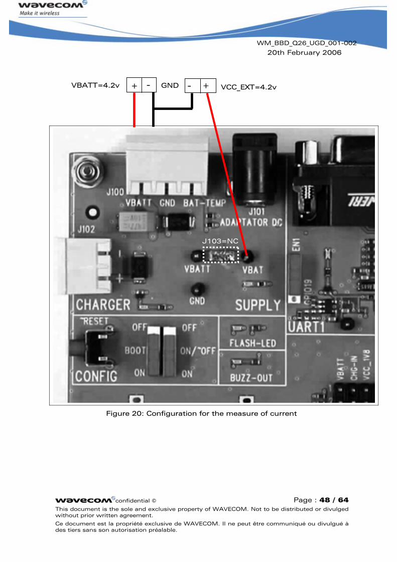
18 Measures of current
To measure the current consumed by the Wireless CPU, use the procedure shown in Figure 20:
Around UART1:
- Remove R408.
- Place R406=0Ω (like R408).
Around UART2:
- Remove R502.
- Place R506=0Ω (like R502).
Around BAT-TEMP:
- Remove R100.
- Do not solder the “special solder”, J103.
- Plug an external power supply like VCC-EXT (=VBATT) on “VBAT”(+), and (GND ) on “GND”(-).
The current consumed by VBATT is ONLY current consumed by the Wireless CPU plugged in.
(All peripherals can be used).
Attention: If the default configuration is conserved, the consumption of this part is around 35 µA.
NOTE: Ensure that the Development Kit is disconnected from the power supply during the work. Use pewter and a soldering iron (ref.WS80 from Weller or similar) to solder.
WM_BBD_Q26_UGD_001-002 20th February 2006
confidential © This document is the sole and exclusive property without prior written agreement.
Ce document est la propriété exclusive de WAVECdes tiers sans son autorisation préalable.
Figure 20: Configuration fo
VCC_EXT=4.2v
J
VBATT=4.2v + + - - G
NDPage : 48 / 64 of WAVECOM. Not to be distributed or divulged
OM. Il ne peut être communiqué ou divulgué à
r the measure of current
103=NC

WM_BBD_Q26_UGD_001-002 20th February 2006
confidential © Page : 49 / 64 This document is the sole and exclusive property of WAVECOM. Not to be distributed or divulged without prior written agreement.
Ce document est la propriété exclusive de WAVECOM. Il ne peut être communiqué ou divulgué à des tiers sans son autorisation préalable.
19 Starting procedure
19.1 Unpacking the Development Kit Q2686 or Q2687 components
There is in the Quik Q26 series box:
- 1 Development Kit Q26 board.
- 1 Wireless CPU soldered, and 1 free. (Q2686 or Q2687 Series)
- 1 SMA/FME antenna connector.
- 1 Power supply connector (3 pins).
- 1 AC/DC adapter .
- 1 RS232 cable.
- 1 USB cable.
- 1 handset.
- 1 RJ9 cable (for handset).
- 1 CDROM with all specifications inside.

WM_BBD_Q26_UGD_001-002 20th February 2006
confidential © Page : 50 / 64 This document is the sole and exclusive property of WAVECOM. Not to be distributed or divulged without prior written agreement.
Ce document est la propriété exclusive de WAVECOM. Il ne peut être communiqué ou divulgué à des tiers sans son autorisation préalable.
19.2 Setting the accessories
Follow the instructions below step by step.
Insert a SIM card into the SIM card holder, J700 (if communications are required).
Make sure that:
o The “ON/OFF” switch is on position “ON”.
o The “BOOT” switch is on position “OFF”.
• Also make sure that:
o The UART1 switch is on “EN1” position.
o The UART2 switch is on “EN2” position.
o The SIM switch is on “SIMPRES” position.
o The all specials solders are soldered.

WM_BBD_Q26_UGD_001-002 20th February 2006
confidential © Page : 51 / 64 This document is the sole and exclusive property of WAVECOM. Not to be distributed or divulged without prior written agreement.
Ce document est la propriété exclusive de WAVECOM. Il ne peut être communiqué ou divulgué à des tiers sans son autorisation préalable.
• Connect the RS232 cable, provided with the Development Kit Q26, between PC port and J400 of the board. (baud rate by default is 115.2 kbps,8N1)
• Connect the antenna to the SMA connector (J202), (if communications are required).
• Connect the handset, provided with the Development Kit Q26, to the Main Audio connector J600 (if communications are required).

WM_BBD_Q26_UGD_001-002 20th February 2006
confidential © Page : 52 / 64 This document is the sole and exclusive property of WAVECOM. Not to be distributed or divulged without prior written agreement.
Ce document est la propriété exclusive de WAVECOM. Il ne peut être communiqué ou divulgué à des tiers sans son autorisation préalable.
19.3 Power supply
• Plug the power supply (via the adapter (J101) or external power supply, 4V/2.5A (J100)).
19.4 Communication test
• Using the terminal emulator, send the following command on COM port to communicate with the Quik Q26 Series: AT↵.
• When the communication is established between the PC and the Wireless CPU, the last one sends the message “OK” as a reply. The message is displayed in the terminal emulator window.
Refer to [4] for communicate between the PC and the Q2686 Wireless CPU.
Refer to [7] for communicate between the PC and the Q2687 Wireless CPU.

WM_BBD_Q26_UGD_001-002 20th February 2006
confidential © Page : 53 / 64 This document is the sole and exclusive property of WAVECOM. Not to be distributed or divulged without prior written agreement.
Ce document est la propriété exclusive de WAVECOM. Il ne peut être communiqué ou divulgué à des tiers sans son autorisation préalable.
20 APPENDIXES


TM3.2P6.5 TM3.2P6.5
COL0/GPIO4
COL1/GPIO5
COL2/GPIO6
COL3/GPIO7
COL4/GPIO8
ROW0/GPIO9
ROW1/GPIO10
ROW2/GPIO11
ROW3/GPIO12
ROW4/GPIO13
KEYPAD
6
5
4
3
2
1
USB-DP
USB-DM
VPAD-USB
USB
SIM-CLK
SIM-IO
SIM-VCC
~SIM-RST
SIMPRES/GPIO18
SIM
MIC1N
MIC1P
MIC2N
MIC2P
SPK1P
SPK2N
SPK2P
SPK1N
AUDIO
SHD-UART1
CT104-RXD1/GPIO37
CT103-TXD1/GPIO36
~CT105-RTS1/GPIO38
~CT106-CTS1/GPIO39
~CT108-2-DTR1/GPIO41
~CT107-DSR1/GPIO40
~CT125-RI1/GPIO42
~CT109-DCD1/GPIO43
RS232 (UART1)
SHD-UART2
CT103-TXD2/GPIO14
CT104-RXD2/GPIO15
~CT105-RTS2/GPIO17
~CT106-CTS2/GPIO16
RS232 (UART2)
BAT-TEMP
BOOT
BUZZ-OUT
CHARGER-LED
CHG-IN
FLASH-LED
~RESET
POWER & APPLI
ON/~OFF
TM3.2P6.5
CONNECTORS
BAT-TEMP
BOOT
BUZZ-OUT
CHG-IN
COL0/GPIO4
COL1/GPIO5
COL2/GPIO6
COL3/GPIO7
COL4/GPIO8
FLASH-LED
MIC1N
MIC1P
MIC2N
MIC2P
ON/~OFF
ROW0/GPIO9
ROW1/GPIO10
ROW2/GPIO11
ROW3/GPIO12
ROW4/GPIO13
SIM-CLK
SIM-IO
SIM-VCC
SIMPRES/GPIO18
SPK1N
SPK1P
SPK2N
SPK2P
USB-DM
USB-DP
VPAD-USB
~RESET
~SIM-RST
GPIO19
~CT109-DCD1/GPIO43
~CT125-RI1/GPIO42
~CT107-DSR1/GPIO40
~CT108-2-DTR1/GPIO41
~CT106-CTS1/GPIO39
~CT105-RTS1/GPIO38
CT103-TXD1/GPIO36
CT104-RXD1/GPIO37
~CT106-CTS2/GPIO16
~CT105-RTS2/GPIO17
CT103-TXD2/GPIO14
CT104-RXD2/GPIO15
GPIO1
GPIO21
AUDIO
KEYPAD
USB
UART2/IO
FULL UART1
SIM
MECHANICS
TM3.2P6.5
FDL
DEVELOPMENT KIT Q26
FDL
GGI
3.0
23/01/05Date:
Version:
Sheet :
SCHEMATIC:
PROJECT:
Made-by:
Verify by:
Validate by:
HIERARCHIC
0/8
TM3.2P6.5
P6P5
PCBPCB=V3.0
P1
P7
P4P3
~CT109-DCD1/GPIO43
~CT125-RI1/GPIO42
~CT107-DSR1/GPIO40
~CT108-2-DTR1/GPIO41
~CT106-CTS1/GPIO39
~CT105-RTS1/GPIO38
CT103-TXD1/GPIO36
CT104-RXD1/GPIO37
CT104-RXD2/GPIO15
CT103-TXD2/GPIO14
~CT105-RTS2/GPIO17
~CT106-CTS2/GPIO16
CHARGER-LED
~RESET
ON/~OFF
SHD-UART2
SHD-UART1
BUZZ-OUT
P9
P2
P8
MIC2P
MIC2N
MIC1P
MIC1N
SPK2P
SPK2N
SPK1P
SPK1N
COL0/GPIO4
COL1/GPIO5
COL2/GPIO6
COL3/GPIO7
COL4/GPIO8
ROW0/GPIO9
ROW1/GPIO10
ROW2/GPIO11
ROW3/GPIO12
ROW4/GPIO13
VPAD-USB
USB-DP
USB-DM
SIM-VCC
~SIM-RST
SIM-CLK
SIM-IO
SIMPRES/GPIO18
BAT-TEMP
FLASH-LED
CHG-IN
BOOT

FDL
DEVELOPMENT KIT Q26
FDL
GGI
3.0
23/01/05Date:
Version:
Sheet :
SCHEMATIC:
PROJECT:
Made-by:
Verify by:
Validate by:
B3S-1100
B3S-1100
B3S-1100
B3S-1100
B3S-1100
B3S-1100
ROW3/GPIO12
NC_SW305-3NC_SW305-5NC_SW305-2
NC_SW304-3NC_SW304-5NC_SW304-2
NC_SW303-3NC_SW303-5NC_SW303-2
NC_SW302-3NC_SW302-5NC_SW302-2
ROW2/GPIO11
NC_SW301-3NC_SW301-5NC_SW301-2
NC_SW300-3NC_SW300-5NC_SW300-2
ROW4/GPIO13
ROW0/GPIO9
COL4/GPIO8
COL3/GPIO7
COL2/GPIO6
COL1/GPIO5
52
43
1
SW305
134
25
SW304
52
43
1
SW303
134
25
SW302
52
43
1
SW301
134
25
SW300
KEYPAD
3/8
COL0/GPIO4
ROW1/GPIO10

GND
GNDGND
GNDGNDGNDGND
MLX67068_4
SHIELD
GND
DM
DP
VBUS
FDL
DEVELOPMENT KIT Q26
FDL
GGI
3.0
23/01/05Date:
Version:
Sheet :
SCHEMATIC:
PROJECT:
Made-by:
Verify by:
Validate by:
SOT23_6
3.3V
VOUT
NCEN
GND
VIN
GREEN
5
43
2
1
U800
1
2
3 4
5
6
D800
10V
C801 C803
6.3V
C802
R802
R801
1
2D801
VBUS
USB
8/8
R803
R800
VPAD-USB
21
J803
21J802
21J801
C800
3
25
1
4
J800
NC_D200-1
VBUS
D+
D-
USB-DM
USB-DP

VCC_1V8 VCC_1V8
FDL
DEVELOPMENT KIT Q26
FDL
GGI
3.0
23/01/05Date:
Version:
Sheet :
SCHEMATIC:
PROJECT:
Made-by:
Verify by:
Validate by:
GND
GND
GND
CCM03
CC4
CLK
GND
I/O
VPP
RST
CC8
VCC
NC_D700-6
SIMPRES
21J705
4
3
5
7
1
6
2
8
J700
NC_D701-6
1 6
5
3 4
2 D701
SIM-VCC
SIMPRES/GPIO18 21J702
SIM-CLK 21J701
SIM-IO 21J703
~SIM-RST 21J704
32
1SW700
5
2
3
1
4
6
D700
SIM
7/8
R700
R701
C701C700
NC_VPP
NC_D701-4

VCC_2V8
GND
GND
GND
GND
GND
GND
GND
FDL
DEVELOPMENT KIT Q26
FDL
GGI
3.0
23/01/05Date:
Version:
Sheet :
SCHEMATIC:
PROJECT:
Made-by:
Verify by:
Validate by:
GND
GND
micn
micp
micn
micp
6/8
MAIN AUDIOSUB AUDIO
R601
R606
R607
R600
1 2
C612
10V
C601
C605
R605
R603
R604
R602
C602
21J603
C600
C604
AUDIO
MIC1N
4
3
2
1
J601
RJ9
21J609
21J608
21J607
21J606
21J605
21J604
21J602
4
3
2
1
J600
RJ9
21
L603
21
L602
21
L601
21
L600
C611
C610
C609
C608
C607
C606
C603
MIC2N
MIC2P
SPK2N
SPK2PSPK1P
SPK1N
MIC1P

VBAT
GND
VBAT
GND
GND
VBAT
GND
GND
GND
GND
GND
FDL
DEVELOPMENT KIT Q26
FDL
GGI
3.0
23/01/05Date:
Version:
Sheet :
SCHEMATIC:
PROJECT:
Made-by:
Verify by:
Validate by:
GND
SUBD8.08_9FCH
RX
DSR
CTS
DCD
RI
GND
TX
RTS
DTR
GND
VBAT
GND
VBAT
VBAT
GND
VCC_2V8
GND;22,23,13,33
C1+
C1-
R1INR1OUT
R2INR2OUT
R3INR3OUT
T1IN T1OUT
T2IN T2OUT
T3IN T3OUT
T4IN T4OUT
T5IN T5OUT
C3-
C3+
SD
C2-
C2+
V+
VCC
V-
EN
VOUT
NCEN
GND
VIN
EMT3
EMT3
NC
A
GND
VCC
Y
D
CP
GND
VCC
Q
INCOMING CALL
YELLOW
pin13 (NC) to GND
ENABLE/DISABLE
RS232
EN1
GREEN
1
2
3
5
4
U401
1
2
3
5
4
U4021
2
3
T400
3
2
1T401
5
43
2
1U403
26
32
1610
1511
1412
4 21
5 20
6 19
7 18
8 17
25
27
2
31
28
29
30
24
1
U400
R405
15KO
15KO
R404
R408
R406
R407
R400
10V
C409
C412C410 1
2
C406
10V
T_P400
V_UART
V_UART
V_UART
V_UART
R401
RI C408
RING
NC_U402-1
2
1
D400
CT103-TXD1/GPIO36
~CT108-2-DTR1/GPIO41
~CT105-RTS1/GPIO38
~CT125-RI1/GPIO42
~CT109-DCD1/GPIO43
~CT106-CTS1/GPIO39
~CT107-DSR1/GPIO40
CT104-RXD1/GPIO37
R402
C402
C401
C404
CT108-2/DTR
CT105/RTS
7
4
3
5
9
1
8
6
2
10
11
J400
21J402
SHD-UART1
RS232 (UART1)
4/8
CT125/RI
12
3
SW400
21J409
21J408
21J407
21J406
21J405
21J404
21J403
C403
C400
C405
CT103/TXD
CT109/DCD
CT106/CTS
CT107/DSR
CT104/RXD
1
2
D401
R403
C407

VBAT
GND
GNDGND
GND
GND
FDL
DEVELOPMENT KIT Q26
FDL
GGI
3.0
23/01/05Date:
Version:
Sheet :
SCHEMATIC:
PROJECT:
Made-by:
Verify by:
Validate by:
SUBD8.08_9FCH
RX
DSR
CTS
DCD
RI
GND
TX
RTS
DTR
VCC_1V8
LQH2MCN100K02L
GND
VBATVCC_2V8
SSOP16_4.9X6_E0.635
T2IN
T1IN
R2OUT
R1OUT
GND VDD
R1IN
R2IN
T1OUT
VCC
VL
SW
VEE
CAP
T2OUT
ON/OFF~
1.8V
VOUT
NCEN
GND
VIN
EN2
GREEN
5
43
2
1
U501
13
14
15
16
8 6
1
2
3
5
12
7
9
10
4
11
U500
T_P500
R506
R502
R503
10V
C505
V_UART_1V8
C501
21
L500
~CT105-RTS2/GPIO17
CT103-TXD2/GPIO14
~CT106-CTS2/GPIO16
CT104-RXD2/GPIO15
2
1
D500
V_UART_1V8R504
R505
R501
R500
NCJ500-1
NCJ500-4
NCJ500-9
7
4
3
5
9
1
8
6
2
10
11
J500
CT105/RTS2
SHD-UART2
RS232 (UART2)
5/8
C506 C508
21J504
21J501
CT106/CTS2
21J503
21J502
1
2
C507
10V
C504
C503
C502
CT104/RXD2
CT103/TXD2
32
1
SW5001
2
3
T500
V_UART_1V8
NCJ500-6

VCC_1V8
GND
GND
VBATT
GNDDC10
WLD8213SW_2
VBATT
GND
GND
VBAT
VBAT
VBAT
FDL
DEVELOPMENT KIT Q26
FDL
GGI
3.0
23/01/05Date:
Version:
Sheet :
SCHEMATIC:
PROJECT:
Made-by:
Verify by:
Validate by:
WLD8213SW_3
VBAT
DO214AA
GND GND
VCC_2V8
DO214AA
EXTERNAL SUPPLY
CONFIG
AC/DC
CHARGER INPUT
VBATT for the module
BUZZER
POWER SUPPLY
CHARGER
RED
YELLOW
GREEN
GREEN
VBAT for the peripherals
SECTOR ADAPTATOR
T_P153
NC_BP100_4
NC_BP100_3
1
2
D105
2
1
D104
2
1
D101
1
2
D100
R103
1
2D102
BUZZ-OUT
ON/~OFF
FLASH-LED
BOOT
CHG-IN
R100
1
2
D103
21J103
T_P157
1
32
J100
2
1
4
3
BP100
POWER + CTRL
1/8
CHARGER-LED
1
2
3
T100
R105
R104
R102
1
2
C100
10V
R101
BAT-TEMP
NC_J101-2
NC_SW101
NC_SW100
32
1
SW101
12
3SW100
21
J102
1
3
2
J101~RESET

GNDGNDGND
VBATT
GND
GND GND
VCC_1V8VCC_2V8
FDL
DEVELOPMENT KIT Q26
FDL
GGI
3.0
23/01/05Date:
Version:
Sheet :
SCHEMATIC:
PROJECT:
Made-by:
Verify by:
Validate by:
VCC_1V8
VCC_2V8
AXK500145J
6-5175472
OUT R107_064_920
ANTENNA
CONNECTOR
EXTERNAL BOARD CONNECTOR MODULE CONNECTOR
NC-5NC-9NC-13NC-7NC-17NC-11NC-15NC-19NC-3
NC-8NC-12NC-16NC-10NC-14NC-18NC-6NC-2GPIO1GPIO2
NC-1 EP-17EP-0EP-2
EP-19
NC-4
J200-81J200-85J200-89J200-93J200-87J200-97J200-91J200-95J200-99J200-83J200-86J200-90J200-94J200-98J200-92J200-96
J200-88J200-84J200-51J200-53J200-42
J200-100
D0D2D4D1D6D3D5D7
D15
D14
D13
D12
D11
D10
D9
D8
~WE-E
A1
~CS2/A25/GPIO1A24/GPIO2
J201-78J201-79
J201-90
J201-80J201-81J201-82J201-83J201-84J201-85J201-86J201-87J201-89
J201-91J201-92J201-93J201-94J201-95J201-96J201-97J201-114J201-115J201-121
EP-4EP-1EP-6EP-3EP-5EP-7EP-18EP-15EP-13EP-11EP-9EP-12EP-10EP-8EP-14EP-16EP-20EP-21
DETAILS OF THE PINS NAMES
ACCORDING TO THE MODULE
J201 J200 Q2686 NAMES ON BOARD
~OE-R/W
~CS3
Q2687
RESERVED
1
IMP200
T_P60
NC-2
NC-6
NC-14
NC-10NC-12
T_P203T_P200 T_P201 T_P202
T_P71
T_P66T_P1
T_P125
NC-5
RESERVED
RESERVED
VBATTVBATT
~CT107-DSR1/GPIO40~CT108-2-DTR1/GPIO41~CT109-DCD1/GPIO43~CT105-RTS1/GPIO38
CT104-RXD1/GPIO37~CT106-CTS1/GPIO39~CT125-RI1/GPIO42CT103-TXD1/GPIO36
NC-1NC-5NC-9
NC-13NC-7
NC-17NC-11
NC-19NC-3AUX-DAC
NC-4NC-8NC-12NC-16NC-10NC-14NC-18NC-6NC-2
SCL/GPIO26SDA/GPIO27
PCM-CLKPCM-SYNC
PCM-OUT
INT1/GPIO25
GPIO23GPIO20
INT0/GPIO3
GPIO24PCM-IN
GPIO21
NC_J201-126
NC_J201-129
BUZZ-OUT
AUX-ADC
SPI2-I/GPIO34
MIC2N
~CT108-2-DTR1/GPIO41
~CT105-RTS1/GPIO38
AUX-DAC
NC_J201-122
GPIO22
706968672
3
575655545352515049484746454443424140393837363534333231302928272625242322212019181716151413
4567
12111098
7172737475767778
120119
7980818283
8584
1181171161151141131121111101091081071061051041031021011009998979695949392919089888786
1
122123124
5859
61
121
60
62636465
125126127128129130
66
J201
NC-15
NC-18NC-16
NC-8
NC-4
NC-19NC-17NC-15NC-13NC-11NC-9NC-7
NC-3NC-1
~CT107-DSR1/GPIO40~CT106-CTS1/GPIO39CT104-RXD1/GPIO37
~CT109-DCD1/GPIO43CT103-TXD1/GPIO36~CT125-RI1/GPIO42
CT103-TXD2/GPIO14
CT104-RXD2/GPIO15~CT106-CTS2/GPIO16
~CT105-RTS2/GPIO17
CT103-TXD2/GPIO14CT104-RXD2/GPIO15
~CT106-CTS2/GPIO16~CT105-RTS2/GPIO17
~SPI1-CS/GPIO31
~SPI1-CS/GPIO31
ON/~OFF
ON/~OFFT_P51 ROW1/GPIO10
ROW3/GPIO12ROW2/GPIO11
NC_J201-61NC_J201-62
MIC1N
GPIO44
987
60
6
59585756555453525150
5
49484746454443424140
4
39383736353433323130
3
29282726252423222120
2
19181716151413121110
1
62646668707274767880828486889092949698100
6163656769717375777981838587899193959799
J200
FLASH-LED
~SIM-RST
AUX-ADC
NC_J201-130
SPI1-I/GPIO30
BOOTBAT-TEMP
NC_J201-128NC_J201-127
NC_J201-125NC_J201-124NC_J201-123
NC_J201-120GPIO19
GPIO2GPIO1
NC_J201-65NC_J201-64NC_J201-63
SPK2N
SPK2PMIC1PSPK1NMIC2NSPK1P
COL4/GPIO8COL2/GPIO6
COL3/GPIO7COL0/GPIO4
ROW4/GPIO13COL1/GPIO5ROW0/GPIO9
USB-DMVPAD-USB
USB-DP
SPI2-IO/GPIO33
SPI2-CS/GPIO35SPI2-CLK/GPIO32SPI1-CLK/GPIO28SPI1-IO/GPIO29
~RESET
FLASH-LED
~SIM-RSTSIM-IO
SIM-CLKSIMPRES/GPIO18
SIM-VCCBAT-RTC
CHG-INCHG-IN
VBATTVBATT
T_P88T_P87
T_P100T_P101
T_P121T_P122
T_P98
T_P103
T_P106
T_P72T_P73
T_P107
T_P74
T_P111T_P110T_P109
T_P6
T_P49T_P50
T_P45
T_P37T_P38
T_P35
T_P33T_P32
T_P28T_P27T_P26
T_P23T_P24
T_P22
T_P20T_P21
T_P19T_P18
T_P3T_P2
T_P4
T_P14
T_P41
T_P43T_P42
T_P39
T_P124T_P123
T_P120T_P119
T_P97
T_P89
T_P96
T_P90
T_P93
T_P91
T_P94
T_P92
T_P95
T_P76
T_P118
T_P116T_P117
T_P114T_P115
T_P112T_P113
T_P105T_P104
T_P102
T_P99
T_P79
T_P82
T_P80
T_P84
T_P81
T_P85
T_P83
T_P86
T_P78T_P77
T_P69T_P68
T_P70
T_P11T_P10
T_P57
T_P59
T_P55
T_P53
T_P40
T_P52
T_P47T_P46
T_P44
T_P31
T_P48
T_P15T_P16T_P17
T_P34
T_P36
T_P30T_P29
T_P54
T_P56
T_P58
T_P12T_P13
T_P9
T_P5
T_P8T_P7
SPI1-CLK/GPIO28SPI1-IO/GPIO29SPI2-IO/GPIO33SPI2-I/GPIO34
SPI1-I/GPIO30SPI2-CLK/GPIO32SPI2-CS/GPIO35
PCM-SYNCPCM-CLK
PCM-INPCM-OUT
INT0/GPIO3INT1/GPIO25
CONNECTORS
2/8
VBATT
R203
R202
BUZZ-OUT
SIM-IOSIM-VCCBAT-RTC
ROW1/GPIO10
GPIO20
J202
ROW2/GPIO11ROW4/GPIO13
COL1/GPIO5COL0/GPIO4
COL4/GPIO8
GPIO24GPIO23GPIO22
VPAD-USBUSB-DPUSB-DM
GPIO21
GPIO2GPIO1
GPIO44SDA/GPIO27SCL/GPIO26
SPK2P
MIC2PSPK1PMIC1NMIC1P
~RESET
SIMPRES/GPIO18
BAT-TEMP
BOOTSIM-CLK
VBATT
CHG-INVBATTVBATT
CHG-IN
ROW3/GPIO12
COL2/GPIO6 COL3/GPIO7
ROW0/GPIO9
SPK1N
SPK2N
GPIO19
T_P25
T_P108
T_P75
T_P67
MIC2P

FDL
DEVELOPMENT KIT Q26
FDL
GGI
3.0
23/01/05Date:
Version:
Sheet :
SCHEMATIC:
PROJECT:
Made-by:
Verify by:
Validate by:
ECR5
ECR4
ECR3
ECR2
ECR1ENT1
MECHANICS
ENT5
ENT4
ENT3
ENT2

WAVECOM S.A. - 3 esplanade du Foncet - 92442 Issy-les-Moulineaux Cedex - France - Tel: +33(0)1 46 29 08 00 - Fax: +33(0)1 46 29 08 08Wavecom, Inc. - 4810 Eastgate Mall - Second Floor - San Diego, CA 92121 - USA - Tel: +1 858 362 0101 - Fax: +1 858 558 5485WAVECOM Asia Pacific Ltd. - 4/F, Shui On Centre - 6/8 Harbour Road - Hong Kong - Tel: +852 2824 0254 - Fax: +852 2824 025


![ON GENERALIZED FIBONACCI AND LUCAS …math.colgate.edu/~integers/q26/q26.pdfn = kx2 for some integer x, then n = 1 or n = 3. We have the following lemma from [5] and [19]. Lemma 5](https://img.pdfslide.us/doc/110x75/5abdfc007f8b9ac0598c9082/on-generalized-fibonacci-and-lucas-math-integersq26q26pdfn-kx2-for-some.jpg)