Embed Size (px)
Citation preview

Research paper
−133−Synthesiology - English edition Vol.11 No.3 pp.133 –145 (Feb. 2019)
In this paper, we explain the development of a system that enables measurement of glossy and mirror surfaces using semiconductor lasers that is the core technology in the development of a laser defect inspection system. Then, we describe the course and the collaborative activities for developing and commercializing the original laser defect inspection system for specific targets including the exterior/interior surfaces of cylinders and the interior of machined holes with various diameters, starting with the surface defect inspection of high-grade steel sheets that was initiated after technological consultation from a regional company. Then, the significance of this development and prospects for the future will be addressed.
2 Course toward development of laser defect inspection system
Ever since 1980, semiconductor laser elements that irradiated at a wide range of wavelengths from ultraviolet to near-infrared light were developed successively, and industrial application of laser beams expanded rapidly. In the field of industrial measurement, in place of the conventional large gas lasers that were vulnerable to impact and vibration, there was growing demand for measurement technology using semiconductor lasers that were small, lightweight, and easy to handle. Based on this background, Okada et al. were motivated to engage in R&D for new industrial measurement technology that efficiently utilized the characteristic of semiconductor lasers.
First, to conduct stable and highly precise measurement of molds and parts that are glossy, high-grade, and with free-form surfaces, Okada engaged in the development of form
1 Introduction
To guarantee that the parts assembled in the automobiles will perform and function as designed, external inspection of the parts is essential. While there is much money spent on automating inspection in anticipation of future labor shortage, there are many areas that remain dependent on visual inspections, and there is strong demand for high-performance automatic inspection technology.[1] Visual inspections are carried out for the inner wall surfaces of machined holes with various diameters of cylinder bores, automatic transmission valve bodies, hydraulic cylinders, and others that are important safety parts of automobiles, since they have particularly strict inspection standards. As no oversight is tolerated, there is demand for high-precision and high-speed automated inspection technology that can detect minute flaws and defects of about 0.1 mm. Systems with various methods have been developed such as eddy current, camera imaging, and laser reflection, but none attained the level that could satisfy on-site demands. Okada et al. have engaged in R&D of advanced industrial measurement systems using semiconductor lasers that are small, lightweight, and easy to handle, and developed new devices that could measure glossy or mirror surfaces that were difficult to measure with conventional measurement technology. Utilizing this experience, and collaborating closely with regional companies, AIST and Sigma engaged in the development of a system to conduct high-speed and high-precision inspection for minute flaws and defects on the inner wall surfaces of machined holes with various diameters, and finally succeeded in developing and commercializing a laser defect inspection system.
An indispensable aspect of manufacturing is the external inspection of all product parts. For example, in the manufacturing of cars, autonomous inspection technology is required to detect minute f laws on glossy or mirror surfaces, which are easily overlooked by visual inspection. In this paper, we report on the history, significance, and future development of an innovative defect inspection system, “ANALYZER,” which has been developed and commercialized. This system utilizes AIST technology—optical diffraction by semiconductor laser—to realize accurate, autonomous inspection of inner wall surfaces of high quality machined holes of various sizes.
Development and commercialization of laser inspection system to detect surface flaws of machined holes
Keywords : Flaw defects inspection system, semiconductor laser, diffracted light, optical fiber, cylinder bore
[Translation from Synthesiology, Vol.11, No.3, p.137–147 (2018)]
Saburo OKADA1*, Osamu NAKAMURA1 and Yasufumi ESAKI2
1. Chugoku, AIST 3-11-32 Kagami-yama, Higashi-hiroshima 739-0046, Japan *E-mail: , 2. Sigma Corporation 9-2-28 Kegoya, Kure 737-0012, Japan
Original manuscript received May 18, 2018, Revisions received July 10, 2018, Accepted July 12, 2018
Research paper : Development and commercialization of laser inspection system to detect surface flaws of machined holes (S. OKADA et al.)
−134−
Synthesiology - English edition Vol.11 No.3 (2018)
measurement based on a coaxial linear displacement method, collaborated with Osaka University. The coaxial linear displacement method has advantages of being less likely affected by specular reflection light, relationship between displacement and output being linear, and precision being unchanging in all measurement ranges. Therefore, there was much expectation for realization, but, as shown in Fig. 1, the realization was hampered by the reduction of precision due to specklesTerm 1 that were characteristics of laser beams.[2] To solve this problem, Okada et al. used a high-density line sensor instead of an area sensor in the photoreceptor as shown in Fig. 2, and created a unique mechanism for rotating the sensor. It was demonstrated that the speckles could be reduced greatly by rotating the line sensor at 200 rpm and conducting space averaging. That is, as shown in Fig. 3, the speckles reduced due to the rotation of the line sensor and the image quality improved, and this allowed the measurement of shapes at precision within 0.1 mm in the measurement range of 150 mm. The light at the end of the tunnel for the road toward realization could be seen.[3]
Next, Okada worked on the development of a noncontact 3D measurement device for mirror surface objects that were more difficult than glossy surfaces. Since mirror objects totally ref lected laser beams and specular points could not be seen at all, it was extremely difficult to measure surface forms, and while measurement could be done for f lat surfaces, there was no measurement device that could
measure curved surfaces. Therefore, Okada devised a method for calculating the 3D coordinates of specular points based on a ray tracing method, by capturing the laser reflection light in multiple positions in 3D space by rotating several position sensitive detectors (PSD) arranged in a dome shape. Figure 4 shows the appearance of the mirror-surface object measurement device[5] that was developed and prototyped. By capturing reflected laser beams in two places of the 3D space by arranging two sets of four PSDs unevenly in a vertical direction, an equation for laser beams that pass through two points in the 3D space was determined. Then, form measurement became possible by setting the intersection point with the irradiation light as a virtual reflection point.[4] A patent was filed for this technology and was registered as intellectual property, and was selected as a notable invention by the Agency of Science and Technology in 2000 (Patent No. 317857, 1999.2).
As Okada was working on the R&D for new measurement technology to utilize semiconductor lasers in industrial measurement, Okada was consulted by a local steel sheet manufacturer about a device to inspect minute f laws and defects in rolled steel sheet surfaces with high glossiness. This launched us into the development of inspection technology using lasers. The requests from the steel sheet manufacturer were the detection of micro-defects of micron order on the surfaces of high-grade rolled steel sheets, the separation of defects and roll marks, and the distinction of detected defect types.
The newly developed laser defect inspection system[5] is shown in Fig. 5. The point of development is the structure for measuring light intensity distribution of the reflected scattered light and diffracted light using a planar photodetector placed at a focal position by gathering all the reflected light within the measurement range to a focal point, and using parabolic cylindrical mirrors in the photoreceptor system in addition to
Fig. 1 Laser beam ring image by area sensorResting state
Rotating stage
1500 3500300025002000Number of pixels of line sensor
Number of pixels of line sensor
Brightness
Threshold
Brightness
Threshold
1500 3500300025002000
Rotating photoreceptor part
Fig. 3 Effect of line sensor rotationFig. 2 Developed and prototyped measurement system

Research paper : Development and commercialization of laser inspection system to detect surface flaws of machined holes (S. OKADA et al.)
−135−Synthesiology - English edition Vol.11 No.3 (2018)
the phototransmitter system of laser beams. As shown in Fig. 6, the multi-segmentation planar photodetector is made by bundling about 3,000 optical fibers of a diameter of 0.5 mm in a semicircular form, and these are divided into four in a radial direction, and into 12 in a circumferential direction. Then light intensity entering a total of 48 blocks is photoelectrically converted using photodiodes. This detector has rougher resolution compared to camera images but is adequate in grasping the characteristics of the reflected light patterns, and also has the advantage that the measurement time per point is high speed at 1 msec or less, and the data volume can be reduced to 1/500 or less.
Of the types of defects produced in steel sheet manufacturing shown in Table 1, the most frequently found scratches and abrasions are shown as examples in Fig. 7 that shows light intensity distribution by LED that was measured by a multi-segmentation planar photodetector and camera images of their reflected scattered light. It was demonstrated that the types of defects could be identified by the multi-segmentation
planar photodetector. Here, linear light in the vertical direction is the diffracted light produced by roll marks, and this is detected on the entire surface of rolled steel sheets. However, since the roll direction is only in one direction in the steel sheet rolling process, the diffracted light of roll marks is produced only in a vertical direction, and this is discriminated from defects by removing the diffraction light that occurs in this direction from the inspection.
Table 1. Type of flaws
Moving tableJackStepping motor
Sample
Parabolic cylindrical mirror
Optical fiber
Multi-segmentation planar photodetector
Laser beam source
Parabolic cylindrical mirror
Vibrating mirror
CCD camera
Planar mirror
Planar mirror
Photoreception systemPhototransmission system
Rust, contamination, abrasionDistributed defect
Scab, sliver, scratch
Linear defect
Roll markPointlike defect
Name of flawForm of flaw
Fig. 5 Laser defect inspection system for flat sheets Fig. 6 Multi-segmentation planar photodetector
PSDPSD
PSD
PSD
PSDPSD
X
Z
r1
r2
d
Position of PSD Measurement principle
Fig. 4 Measurement system for curved mirror objects

Research paper : Development and commercialization of laser inspection system to detect surface flaws of machined holes (S. OKADA et al.)
−136−
Synthesiology - English edition Vol.11 No.3 (2018)
This technology has been filed for patent and registered as intellectual property (Patent No. 2073658, 1996.7).
3 Development of defect inspection system for inner wall surfaces of machined hole
What triggered machined hole inspection was technological consultation from an automobile parts manufacturer in Hiroshima around 1998, about the inspection of minute flaws and defects in the inner walls of automobile hydraulic master cylinders that were parts manufactured by the company. The target was a cylindrical part with an inner diameter of 25 mm, depth of 150 mm, and a mirror-polished inner wall. Since it was hard to view the inner wall by visual inspection and minute defects were often missed, Okada decided to conduct the inspection using laser beams. Since the target part was cylindrical and rotatable, the device shown in Fig. 8 was made as a prototype.[6] If there were no defects when the finely focused laser beam is irradiated onto the inspected surface, the laser beam reflects off without scattering. On the other hand, if there was a defect, the light that hit the defect scatters widely outside the specular reflection light. We realized that if optical fibers were installed in a position in which specular reflection light could be received and a position in which only scattered light could be received, the two lights could be separated. Therefore, the specular
reflection light and scattered/diffracted light were separately received with optical fiber bundles with a diameter of 0.5 mm arranged along the circumference of two concentric circles of a diameter of 5 mm and 15 mm from the center of the reflected laser beam.
Figure 9 shows the panorama images of light intensity data that are shown in a circumferential direction and sampled at 0.2 mm intervals. The image in (a) is the light intensity of the specular reflection light and (b) is the light intensity image including the scattered and diffracted light. The (a) image clearly shows spiral indentation defects caused by broken cutting bites, and (b) shows a scratch. It was shown that various defects could be detected at high sensitivity by using specular reflection light and scattered light. The black and grey holes are oil holes and are not defects.
Around the same time, President Shitanaka of Sigma Corporation, an automobile parts manufacturer in Kure City, saw the laser defect inspection system that was exhibited at a patent fair. He became interested in semiconductor lasers and requested whether this device could be used for external defect inspection for mass-produced automobile parts with cylindrical shapes. Sigma mass produced small automobile parts and was working on automating inspection with the aim of zero shipment of defective products. It was looking
(Abrasion)(Scratch)(Normal)
Fig. 7 Differences in diffraction pattern by flaw types and examples of measurement by multi-segmentation planar detector
Fig. 8 Inspection system for inner wall surfaces of machined holes
Inspection surface
Mirror
Optical fibersSpecular reflection light
Incident laser beam
Lens
Diffracted lightHydraulic master cylinderInspection probe

Research paper : Development and commercialization of laser inspection system to detect surface flaws of machined holes (S. OKADA et al.)
−137−Synthesiology - English edition Vol.11 No.3 (2018)
into introducing a laser defect inspection system that could inspect small defects.
Joint research was started in 2000, and the laser defect inspection system for external defects of cylindrical parts was jointly developed by AIST and Sigma in 2002. Figure 10 shows the device. Since the external inspection system using laser beams exceeded expectations in small defect inspection, President Shitanaka proposed to start a business to commercialize and sell the laser defect inspection system
that was not yet known in society, and to jointly develop a new laser defect inspection system for the inner surfaces of cylinder bores for automobile manufacturers.
4 Acceleration of R&D through the establishment of collaborative research unit
In 2001, research institutes under the Agency of Industrial Science and Technology, Ministry of International Trade and Industry underwent a major re-organization into the
Fig. 10 Inspection system for outer surface flaws of cylindrical automobile parts
Inspection probe
Cylindrical parts
Fig. 9 Examples of inspection images of inner wall surfaces of machined holes
Indentation flaw
Hole
Hole
Hole
Circumferential direction
Circumferential direction
Scratch
80(mm)6040200
0
20
40
60
80
(mm)
20
40
60
80
(mm)
0
Axial
direction
Axial
direction
80(mm)6040200
(b) Light intensity image of scattered light and diffracted light
(a) Light intensity image of specular reflection light

Research paper : Development and commercialization of laser inspection system to detect surface flaws of machined holes (S. OKADA et al.)
−138−
Synthesiology - English edition Vol.11 No.3 (2018)
National Institute of Advanced Industrial Science and Technology (AIST). In 2003, AIST Chugoku set a policy of placing importance on biomass research, the researchers for manufacturing were transferred to other centers, and we stood at a major crossroad of whether to continue or discontinue the R&D for laser defect inspection system right before its realization. When Okada et al. were seeking a solution, President Shitanaka of Sigma who was certain about the future of laser defect inspection strongly requested the continuation of the development, and he was also willing to provide research funds. After discussing with Director-General Yabe (at the time) of AIST Chugoku and the researchers who were transferred to Tsukuba, AIST agreed to continue the R&D based on the funds provided by the company after setting up a collaborative research unit that would be the base of R&D at the Industry Academia Government Collaboration Promotion Division, AIST Chugoku, and we applied for its establishment. There were many conditions for application: there must be requests from many companies; pure private company funds will be provided for three years to fulfill AIST’s rules; there must be a clear research goal, and impact on industry, and the project must be achievable by joint research; and there must be research capacity at AIST. The hurdles to clear were high, but the establishment of a collaborative research unit for laser application functional diagnosis was accepted for three years starting in 2004.
The research goal was set as the R&D and product realization of a laser defect inspection system for the inner wall surfaces of automobile cylinder bores, to meet the demands from the automobile manufacturers. The eddy current and optical inspection systems for cylinder bore interior that were commercially available at the time did not satisfy the on-site demands, and a higher-performance and higher-functional inspection system was desired. Figure 11 shows the inspection system of cylinder bore interior that was developed and prototyped through one-year joint research with the basic concept provided by AIST. The key of the development is the structure in which the inspection probe
rotating at 1500 rpm is lowered at a steady rate along the central axis of a hole, a semiconductor laser beam formed into a true circle of a diameter of 0.1 mm is irradiated perpendicularly onto the wall surface, the specular reflection light, reflected scattered light, and diffracted light from the wall surface are collected by optical fibers arranged in double concentric circles, light intensity is measured by an optical sensor installed at the other end of the optical fiber, and the defects are detected by light intensity change.[7][8] Since the structure of the probe tip greatly affected the performance, much time and effort were needed for repeated experiments done by changing the tip form and end face position of the optical fiber. However, through the efforts of the development personnel at Sigma, the collaborative research unit was able to find the optimal position and form. Also, the probe tip was made removable, and by employing a structure in which the tip could be slid back and forth, the device could measure a wide-range of inner diameters from 40 mm to 150 mm.
Figure 12 shows the light intensity of specular ref lection light measured by inner optical fibers, and Fig. 13 shows the image of the light intensity of scattered light measured by outer optical fibers, and the light intensity data of one rotation. The inspection target was a cylinder bore with an inner diameter of 60 mm, and the measurement was done in 0.2 mm intervals in both the circumferential direction and axial direction. The measurement points were about 4,000 points per rotation, 600 lines in the axial direction, and total data volume was 2,400,000 points (5 megabytes). A clear difference in light intensity distribution between the specular reflection light and scattered light images can be seen.
In the two figures, the figures shown at the bottom is the actual value (blue or red line) of each light intensity per rotation, the maximum and minimum of the thresholds automatically calculated using the actual values are shown in yellow and green lines, and the parts that surpass this range at the top and bottom are candidates of defects. The reason the maximum and minimum are set is because the laser beam is scattered and the light intensity is decreased below
Fig. 11 Inspection system for inner wall surfaces of machined holes
Fixed part
Fixed part
Probe structureProbe tipInspection probeAppearance of inspection device

Research paper : Development and commercialization of laser inspection system to detect surface flaws of machined holes (S. OKADA et al.)
−139−Synthesiology - English edition Vol.11 No.3 (2018)
the minimum for the specular reflection light image in most defects, while he light intensity increases and may surpass the maximum in the case of glossy defects. Similarly, even in the scattered light image, the defect candidates are the parts in which the scattered light surpasses the upper and lower limits. Here, investigation was done for the difference in response against surface contamination and color between specular ref lection light and scattered light using a white tape. In the specular ref lection light image, the reflection light intensity increased due to the white tape and was judged as a candidate of a glossy defect, but in the scattered light image, the laser beam did not scatter on the tape surface, the light intensity change was small, and it was judged to be not a defect. Also, in the case there are small holes on the surface, both specular reflection light and scattered light
decrease, and they can be judged as defects. As it can be seen, the reliability of inspection could be increased using the two inspection images, and it was extremely effective in preventing erroneous judgment.
In order to conduct the collaborative research activities smoothly and efficiently, the collaborative research unit made efforts to maintain the line of communication by holding a progress meeting which the President attended every other month, gave reports on the development status, and opinions were exchanged about the technological issues, the measures, and long- and short-term development processes. Occasionally, the President determined the policy. Also, if any problems arose, emergency meetings were held by the personnel-in-charge, to conduct quick review and changes of
Fig. 12 Light intensity detection image of specular reflection light
Fig. 13 Light intensity detection image of scattered light
20
40
60
(mm)
0
50 100 150 2000 250(mm)
Circumferential direction
Number of pixel
Axial
direction
Light intensity
White tape
50 100 150 2000 250(mm)
20
40
60
(mm)
0
Circumferential direction
Number of pixel
Axial
direction
Light intensity
Research paper : Development and commercialization of laser inspection system to detect surface flaws of machined holes (S. OKADA et al.)
−140−
Synthesiology - English edition Vol.11 No.3 (2018)
plan. In the case of this project, since the research funds were the matching funds provided by the private company and AIST, necessary items could be procured quickly without concern of the budget, and so the development progressed quickly.
5 Start of laser defect inspection system business and commercialization of ANALYZER
In 2005, Sigma newly established the Division of Laser Defect Inspection System, started sales of the laser defect inspection system, and steadily increased sales from six systems in 2006 to 11 in 2007. To strengthen the sales, Esaki assumed the position of Division Manager. However, hit suddenly by the economic recession due to the Lehman Shock of October 2008, the device did not sell well, the performance of the main business dipped greatly, and the collaborative research unit faced a major crossroad of whether to continue or to retreat from the defect inspection business.
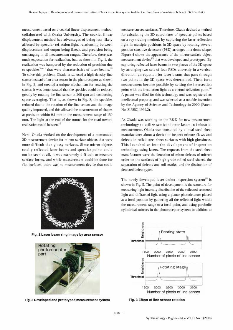
As a measure to discern the future of the project, Esaki set off to visit the companies that purchased the system as well as other machining companies to survey the potential demands for the laser defect inspection system. He found that there was large, unexpected potential demand for the inspection of small holes with inner diameters of 20 mm or less that was outside the target of this system, and that there was need to shorten the inspection time per part from the conventional 30 sec to within 10 sec in order to match the on-site cycle time, because there were many holes that had to be inspected in the small bore hole inspection for automobile parts. These points were noted, and the collaborative research unit proposed the continuation of business to the President and suggested that essential modification be made during the recession, such as reducing the size of the inspection probe and achieving high-speed inspection. These were put to immediate practice after
Fig. 14 Modification of inspection probe Fig. 15 Example of developed defect inspection system
Optical fiber
Small diameter probe (probe diameter of 6 mm)
High-speed hollow motor (15,000 rpm)
ANALYZER robotANALYZER (probe diameter 2.3 mmΦ)
ANALYZER (probe diameter
6 mmΦ)
receiving a green light from the President.
For the achievement of high-speed inspection, instead of the belt-driven method using an external motor that was the damper to high speed, we newly developed a hollow motor that enabled high-speed rotation of the probe. As a result, the rotation of the inspection probe was increased to about 10 times or 15,000 rpm, and we succeeded in shortening the inspection time to the target 10 sec or less.
Next, for decreasing the probe size, Sigma newly developed a small diameter probe based on AIST’s advice. As shown in Fig. 14, the position of the optical fiber was changed, and the tip was changed from L-shape to straight. The probe diameter was reduced to 6 mm, but to supplement the decrease of receiving light intensity accompanying the reduced number of optical f ibers, the photodiode that photoelectrically converted the received ref lection light was changed to a high-sensitivity, and high-speed element. By reducing the probe diameter, the obtainable inspection images were only scattered light images, but the level of completion of the product remarkably improved by strengthening the feature value analysis function for the planar form of the abnormal part that surpassed the threshold and by improving the algorithm, and so the defect judgment condition could be adjusted finely.[9]
By 2010, the economy was clearly recovering, and Esaki restarted sales by naming the product ANALYZER (this is a play on words in which a Japanese word, “ana,” for holes is used). The orders came in widely from not only the automobile related companies but also companies of various businesses, and the number of sales increased rapidly. Matching users’ demands, a standard type of a diameter of 6 mm, a thin type of a diameter of 2.3 mm, and an ANALYZER robot were developed and sold successively. The sales results reached over 200 systems in total.

Research paper : Development and commercialization of laser inspection system to detect surface flaws of machined holes (S. OKADA et al.)
−141−Synthesiology - English edition Vol.11 No.3 (2018)
Sigma became the top selling company of this niche market of defect inspection systems for interior of holes in Japan, but as shown in Table 2, various hole interior inspection systems with diverse methods were sold in Japan. However, there was no uniformity in performance indication, and the user companies were confused. Esaki felt the need for standardization of defect inspection systems and started activity for standardization in Japan. In 2015, a committee for drafting the proposal for standardization was established with the support of the Hiroshima Industrial Promotion Organization. Device manufacturers and user companies were asked to participate, and an application was submitted to the standardization system for the creation of new markets of the Japanese Industrial Standards Committee. The proposal was accepted, and the discussions for standardization are currently in progress.
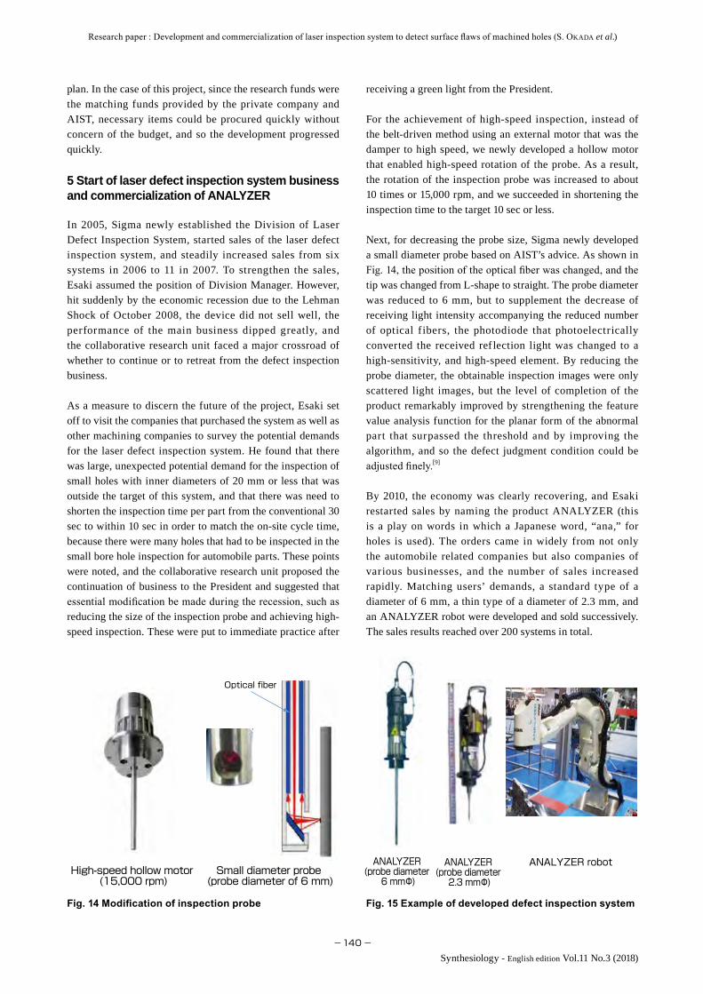
6 Scenario for road to industrial application of semiconductor lasers
Star ting with technological consultation from a local company, the collaborative research unit launched R&D for a laser defect inspection that was demanded by industry. Figure 16 shows the f low of product realization through technological development at AIST and collaboration with Sigma explained above. First, to realize defect inspection for inner walls of small and glossy cylindrical parts, we developed a high-sensitive inspection system that separated and measured the diffracted light unique to laser beams that were produced by defects. However, just before commercialization, continuation of R&D seemed difficult due to the re-structuring of AIST, but the development and
product realization of a laser defect inspection system of a probe rotating type were continued by establishing a research organization called a collaborative research unit. However, due to the Lehman Shock that occurred suddenly, Sigma faced a crisis of retreat from business, but the policy was changed to meet the demands for inspection of the interior of small holes. As a result of developing a high-speed laser defect inspection system for holes with small diameters that matched the demands of companies, business expanded rapidly. Currently, utilizing the standardization system for the creation of new markets, domestic standardization is being conducted by calling on others in the same industry, and we are also preparing for international standardization in anticipation of overseas expansion.
There were two large turning points in the development and commercialization of the laser defect inspection system. Difficulties were overcome by the ingenuity of AIST and a local company, and Sigma was able to send out the ANALYZER to the world. The device system was purchased by automobile manufacturers such as Toyota Motor Corporation, Honda Motor Company, Ltd., Mazda Motor Corporation, and others, as well as automobile parts manufacturers including Denso Corporation, Aisin Seiki Co., Ltd., Mitsubishi Heavy Industries, Ltd., and others. Sales are increasing to foreign companies such as Daimler AG.
7 Development of next-generation inspection system through collaboration crossing regional centers
AIST sets its impor tant goal as the development of
Table 2. Commercially available inspection systems for inner wall surfaces of machined holes (from HPs of respective companies)
Characteristic
Laser reflection typeCamera imaging typeCamera imaging typeLaser reflection typeEddy current typeMeasurement principle
Sigma CorpCompany DCompany CCompany BCompany AName of manufacturer
Two ND probes are arranged facing each other at 180° to detect cavities and cracks, and four air jets are arranged facing each other at 90° to measure interior diameters. It is necessary to change the probe diameter according to the work piece diameter. Applicable diameter of hole: 40 mm or more.
Laser beam is irradiated on one of the two optical fibers, the beam is focused to 50 μm using the lens at the tip and irradiated perpendicular to the interior metal surface, specular reflection light is collected with another fiber, and light intensity is measured by PD. The entire inner surface of a hole is inspected by high-speed rotation of a 45° mirror on the probe tip. The focal depth is shallow since the lens is short-focus. Applicable diameter of hole: 2 mm or more.
The characteristic is to shoot fine images inside cylinders with a high resolution area camera and light rotation mechanism in which several mirrors are rotated in synch. The structure is complex. Applicable diameter of hole: 60 mm or more.
The tip of an acrylic rod is machined into an inverted cone shape, the inner wall surface is illuminated with a ring lamp from the other end, an image of the inner wall projected on the conical surface of the tip is shot with a camera, and defects are inspected by image processing. It is compact and lightweight since there is no rotating part. Applicable diameter of hole: 6 mm ~60 mm.
Laser beams are irradiated perpendicularly to the inspection surface using a long-focus lens, part of specular reflection light is irradiated on several optical fibers that are arranged along the circumference at the probe tip, light intensity is measured by PD, and defects are determined by changes in light intensity. Since a long-focus lens has deep focal depth, there is no reduced sensitivity due to displacement. Applicable diameter of hole: 4 mm or more.
Research paper : Development and commercialization of laser inspection system to detect surface flaws of machined holes (S. OKADA et al.)
−142−
Synthesiology - English edition Vol.11 No.3 (2018)
“technology transfer research” in the 4th medium-term goal period, to clarify the mission for functioning as an institution of technology transfer to create innovation. The regional centers of AIST set the main research themes considering the characteristics of regional industrial clusters, and conduct R&D at the highest level. They also collaborate with the regional economy and industrial bureaus and public research institutions, understand the demand of the small and medium-sized companies as well as regional core companies, and aim to contribute to regional revitalization by conducting technological transfer through involvement of all of AIST.[10]
At AIST Chugoku, “ AIST Chugoku Network Club (San’yu Kai in Japanese)” consisting of small and medium-sized companies, major companies, and public research institutions of f ive prefectures in the Chugoku region and other stakeholders was set up in 2011 for collaborative activities such as network formation, and a scheme[11] to extract issues of companies in the Chugoku region by actually visiting sites
Fig. 16 History of commercialization through technological development by AIST (blue) and collaboration with Sigma (green)
Demand for inspection of inner surfaces of small diameter holes
Demand for inspection of glossy inner surfaces of hydraulic master cylinders Separation technology
for reflected/diffracted light
Industrial application of semiconductor lasers to measurement and
inspection technologies
Survey of potential demands
Lehman Shock
Organization of collaborative research unit
Re-organization of AIST
Demand for inspection of inner surfaces of cylinder bores
Demand for defect inspection of steel plates
Demand for mirror curved surface measurement
Demand for glossy curved surface measurement
Top seller in global niche market
Sales of ANALYZER; became top seller in domestic niche market
Start sales of cylinder bore
inspection system
Start joint development of cylinder bore inspection system
Introduction to company’s automobile parts inspection
Standardization
Hollow motor employment and technology for downsizing probe
diameter
High-speed rotation technology and
automatic judgment algorithm
Separation technology for reflected/diffracted light in a rotating optical system
Measurement technology for 2D light intensity distribution by reflected scattered/diffracted
light
Spatial measurement technology with two sets of PSD and four elements
Speckle noise reduction technology
was established.
AIST became estranged from Sigma after the collaborative research unit broke up as the researchers were dispatched to other places. However, in 2011, there was a top meeting between Director-General Nakamura (at the time) of AIST Chugoku and President Shitanaka in which the President requested whether AIST could solve the problem of erroneous or excessive judgment. Nakamura selected a suitable researcher at AIST Kyushu among the researchers of AIST around Japan and the development of a defect inspection system that could tell defects and contamination was started in 2012, and an improved laser defect inspection system was developed and realized with new ideas. With further collaboration with AIST Kyushu, we are working enthusiastically on the development of a next-generation inspection system that is also capable of quality control, and it is expected that we shall have a world-dominating product in not-so-distant future through collaboration that crosses regionality.
Acknowledgement
We shall take this opportunity to thank all the people who were involved in the R&D and commercialization of this laser inspection system. We do hope this paper will contribute to further promotion of future technological transfer activities.
Terminologies
Term 1. Speckle: Dot pattern that appears when coherent light like a laser beam is scattered by an object. It is often the cause of reduced precision in image measurement and is extremely difficult to remove. It is also called speckle noise.
References
[1] Chugoku Industrial Innovation Center: Monzukuri kigyo seisan genba ni okeru kensa no jidoka sokushin kanosei chosa hokokusho (Report of the survey on the possibility for promoting automated inspections at the production sites of manufacturing industries) (2016) (in Japanese).
[2] T. Miyoshi, Y. Takaya, N. Takizawa and R. Fukuzawa: Development of non-contact profile sensor for 3-D free-form surfaces (3rd Report): Optical ring image 3-D profile sensor, Journal of Japan Society for Precision Engineering, 61 (2), 258–262 (1995) (in Japanese).
[3] S. Okada, M. Imade, H. Miyauchi, T. Miyoshi, T. Sumimoto, and H. Yamamoto: Noncontact 3D shape inspection based on optical ring imaging system, Proceedings of SPIE, 2909, 58–65 (1997).
[4] S. Okada, M. Imade and H. Miyauchi: Kyomen buttai no hyomen-keijo to hosen vector no doji keisoku system no kaihatsu (Development of the simultaneous measurement system for normal vector and surface form of mirror-surface

Research paper : Development and commercialization of laser inspection system to detect surface flaws of machined holes (S. OKADA et al.)
−143−Synthesiology - English edition Vol.11 No.3 (2018)
history of R&D at AIST and the development and realization of the laser defect inspection system.
Osamu NAKAMURACompleted the master’s course at the Graduate School of Agriculture, Kyushu University in 1979. Assistant professor, Department of Oral Biochemistry, Dental School, Kagoshima University in 1979; Visit ing Researcher, Case Wester n Reser ve Un iversi t y i n 1989 –1991; Research Fel low, Ky ushu Nat ional Industrial Research Institute, Agency of Industrial Science and Technology, Ministry of International Trade and Industry in 1997; Director, Bioresource Division and Director General, Biotechnology and Food Research Institute, Fukuoka Industrial Technology Center in 2001; Director, Technology Evaluation and Research Division, Ministry of Economy, Trade and Industry in 2005; Deputy Director, Evaluation Department, AIST in 2007; Director, Science and Technology Promotion Division, Nagasaki Prefectural Government in 2009; Director-General, AIST Chugoku in 2011; and Supervisory Innovation Coordinator, AIST from 2014. Doctor of Dentistry (Osaka University). In this paper, he was in charge of the structure of this paper and writing about the collaboration between regional centers and companies.
Yasufumi ESAKIGraduated from Tsuru University in 1988. Joined a company formed as a result of merger of a major communication company and foreign company in 1988; and worked in sales at a city bank. Joined Sigma Corporation in 2002; Manager of President’s Office and Deputy Manager of Secur ity Business Division; and currently, Chief Operating Officer, Sigma LIS Company. As the person-in-charge for promoting the development of mass production and business at the company side, has found important customers among automobile manufacturers and parts manufacturers, and was involved in the sales of over 200 inspection systems. In this paper, he was in charge of writing about needs and wants of companies, collaboration with AIST, and results of commercialization.Authors
Saburo OKADAComple ted t he mas te r’s cou r se a t the Graduate School of Engineering, Hiroshima University in 1974. Joined G ove r n m e n t I nd u s t r i a l Re s e a r ch Institute, Chugoku, Agency of Industrial Science and Technology, Ministry of International Trade and Industry in 1974. Engaged in R&D for various hydraulic measurement devices pertaining to the Seto Inland Sea Hydraulic Model. Since 1995, engaged in R&D for measurement devices using semiconductor laser. Coordinator, Industry Academia Government Collaboration Promotion Division, AIST (in charge of metrology standard) in 2005; retired in 2008; coordinator at a public incorporated foundation; and currently working as industry-academia-government collaboration staff at AIST Chugoku from 2014. Doctor of Information Engineering (Kyushu Institute of Technology). In this paper, he was in charge of writing the
object), Proceedings of the 3rd Symposium on Sensing via Image Information, 319–322 (1997) (in Japanese).
[5] S. Okada, M. Imade, H. Miyauchi, T. Sumimoto and H. Yamamoto: A Combined Image Inspection System with Discrimination of Various Kinds of Surface Defects, The Transactions of the Institute of Electrical Engineers of Japan, C, A publication of Electronics, Information and System Society, 115 (3), 452–459 (1995) (in Japanese).
[6] S. Okada, M. Imade and H. Miyauchi: Laser-ko kaisekiho ni yoru yuatsu cylinder naiheki kyokumenjo no bisho-kizu kensa sochi no kaihatsu (Development of the micro-defect inspection system for the curved inner wall surface of hydraulic cylinder by laser beam diffraction method), Proceedings of Intelligent Mechatronics Workshop, 6, 151–156 (2001) (in Japanese).
[7] S. Okada: Kaisetsu laser-ko kaisekiho ni yoru bisho-kizu kensa system (Explanation of micro-defect inspection system using the laser beam diffraction method), Kensa Gijutsu (Inspection Engineering), 9 (3), 8–13 (2004) (in Japanese).
[8] S. Okada: Laser-ko kaisekiho ni yoru cho-koseido bisho-kizu kekkan kenshutsu sochi (Ultra-high-precision micro flaw and defect detection system by laser beam diffraction method), Jidosha Gijutsu (Journal of Society of Automotive Engineers), 56 (4), 84–85 (2002) (in Japanese).
[9] Y. Esaki: Handotai laser o shiyo shita kizu kensa sochi no inline katsuyo (Inline utilization of the flaw inspection system using semiconductor laser), Kensa Gijutsu (Inspection Engineering), 12, 64–67 (2011) (in Japanese).
[10] O. Nakamura: Chiiki-hatsu innovation soshutsu no PDCA: Sansoken chiiki center no torikumi o jirei ni shite (PDCA for region-initiated innovation creation: Case studies of efforts by AIST regional centers), Proceedings of the Annual Conference of the Japan Society for Research Policy and Innovation Management, 31, 349–352 (2016) (in Japanese).
[11] AIST: Chiiki center no renkei de jitsugen shita sekai top class no technology: Global shijo de tatakaeru koseido na laser kizu kensa sochi “ANALYZER” (World top class technology realized through the collaboration of regional centers: ANALYZER, the high-precision laser defect inspection system that can challenge the global market), LINK, 4, 10–15 (2016) (in Japanese).
Discussions with Reviewers
1 OverallComment (Keiichi Ikegami, AIST)
This paper discusses the course of development and commercialization of a device system that conducts automatic and high-precision f law and defect inspection of glossy and mirror surfaces, which are optically difficult to inspect, of inner walls of holes with various diameters. The “points of development” are clearly stated for each stage leading to the final commercialization, and the technical progress is described comprehensibly. In addition to technological hurdles, the ways in which unexpected hurdles such as the re-organization of the research institute and the Lehman Shock were surmounted are described, which makes this paper very thought-provoking.Comment (Ken’ichi Fujii, AIST)
This research is very valuable on the point that automated
Research paper : Development and commercialization of laser inspection system to detect surface flaws of machined holes (S. OKADA et al.)
−144−
Synthesiology - English edition Vol.11 No.3 (2018)
inspection technology for glossy and mirror surfaces was developed, because flaws and defects were often missed in visual inspections of inner surfaces of holes with various diameters of industrial parts used in automobiles and others. This is a detailed report to show the process and the significance of using AIST’s technological potential applying semiconductor laser diffraction, in order to develop an innovative defect inspection system, and to succeed in its commercialization. Particularly, this paper mentions that with overcoming crises such as re-organization of AIST and Lehman Shock, it was very effective to conduct product development matching demands of customers. This paper is an excellent paper that thoroughly discusses the scenario for successful product realization.
2 Demand for automated inspection technologyQuestion (Ken’ichi Fujii)
In Chapter 1, you write, “Visual inspection is done for the inner wall surfaces of machined holes with various diameters that are drilled in cylinder bores, automatic transmission valve bodies, hydraulic cylinders, and others that are important safety parts in automobile industry, since they have particularly strict inspection standards. As no oversight is tolerated, there is demand for high-precision and high-speed automated inspection technology that detects minute flaws and defects of about 0.1 mm.” Please provide an easy-to-understand scale that shows the degree of effect of cost reduction through this automation, as well as the amount invested as cost to this type of inspection system by the automobile industry.Answer (Yasufumi Esaki)
The cost of the system to realize automated inspection for valve bodies (transmission parts) is 15 million to 20 million yen/system. This system automates valve body hole inspection. In fact, about 60 % of the total items of inspection of valve bodies have become automated with this technology.
On the other hand, the normal cost of inspection personnel is about 10 million yen/person/year. Normally, hole inspection of valve bodies is conducted by four people/set, so automation will generate cost reduction of 40 million yen (10 million yen x 4) per year. Of course, improvement of quality was realized at the same time.
3 Development of defect inspection system for inner wall surfaces of machined holesQuestion (Ken’ichi Fujii)
In Chapter 3, you write that you developed the technology for inspecting the inner wall surfaces of machined holes with excellent ideas such as installing optical fibers in the position in which specular reflection light can be received and the position in which only scattered light can be received, as shown in Fig. 8. What were the background and process that led to such ideas?Answer (Saburo Okada)
When the authors were engaging in the research aiming to develop a noncontact shape measurement device as a new industrial measurement system utilizing characteristics of semiconductor lasers at the time, we got a request from a local steel sheet manufacturer on whether it was possible to realize a method and technology that could detect micro-defects of micron order on the surface of high-grade rolled steel sheets, and could also identify the difference between defects and roll marks. Therefore, we decided to develop an inspection system using laser beams. The issue at the beginning was the development of a sensor that allowed quick and efficient measurement of two-dimensional distribution of laser ref lection light. At the time, it was difficult to obtain a special sensor that used concentric photodiodes developed in the USA. Instead, we devised an
inexpensive sensor that we made ourselves. It was a multi-split planar detector made by bundling optical fibers, as shown in Fig. 6, and the objective was fulfilled.
During the same period, an automobile parts company requested the development of an inspection system for parts with mirror treatment on the interior of cylinders with a diameter of 25 mm and a depth of 150 mm. Using the reflection light image of Fig. 7 as a hint, we came up with a device shown in Fig. 8. Moreover, by increasing the focus depth by focusing the light gradually by long-focus lens after putting 200 mm or more of distance between the laser source and the flaw surface, and by optimizing the thickness, number, and tip position of the optical fibers, and after much trial-and-error, we were able to efficiently separate specular reflection light, scattered light, and diffracted light, and were able to greatly improve inspection performance.Comment (Keiichi Ikegami)
The principle of this device has been mostly covered in Chapter 3, but I think the technological highlight of this paper is presented in Figs. 12 and 13. I think it will be more useful to the readers if you provide more detailed explanation featuring these figures.Answer (Saburo Okada)
I added detailed explanations to Figs. 12 and 13.Question (Keiichi Ikegami)
It seems that by reducing the diameter of the probe, the geometric condition for separating specular reflection light and diffracted (scattered) light became stricter. How did you work around this? If you could explain to the extent you are allowed, I think it will be easier to understand.Answer (Yasufumi Esaki)
As a countermeasure against the reduction of data types, we made it possible to finely set the judgment conditions by adding algorithms. Every year, we improve the percentage of correct answers by adding 25 to 30 functions. At the same time, we also worked on the improvement of reception efficiency of laser irradiation and ref lection light, to improve the quality of the obtained data.
4 Key to overcoming crisesQuestion (Ken’ichi Fujii)
You write that the collaborative research unit was established due to the re-organization of AIST in 2003, and that the potential demand survey was conducted during the recession period after the Lehman Shock to gain understanding of the potential demands such as for hole diameters of 20 nm or less and further time reduction, and these were greatly useful in the later product realization. You succeeded in downsizing the probe by developing a hollow motor as new transfer technology during the time, and this led to good sales performance after 2010 by increasing the degree of completion of the product. I imagine that there was much difficulty in starting new development during the economic recession. What were the way of thinking and policy that became the key?Answer (Yasufumi Esaki)
During recession, the most important thing, I think, is how to prepare for the time when the economy improves. There was plenty of time due to slow business during recession, and we already knew the business potential of this inspection system due to our own surveys and projections. Therefore, I was thinking about how to push the business forward in the minimum time possible. First, we narrowed down the target, and set aim on the critical parts and important safety parts of automobiles. That is because we expected that the car companies would spend a lot of budget on automated inspection for parts subject to 100 % inspection in which there was no tolerance for oversight.

Research paper : Development and commercialization of laser inspection system to detect surface flaws of machined holes (S. OKADA et al.)
−145−Synthesiology - English edition Vol.11 No.3 (2018)
Next, since there was a limit to the manpower at the venture division of small and medium-sized companies, we conducted benchmark tests against competitive products, considered in which part we could differentiate ourselves in the parts inspection mentioned above, and set priorities to development topics that had high impact and high possibility of realization.
That is, we believed that if we narrowed down the target work that was most applicable to this inspection system, and if we could create a system that surpassed anything that the competitors had, we would be able to push the business forward when the economy improved.


![[Bob flaws] the_tao_of_healthy_eating_dietary](https://img.pdfslide.us/doc/110x75/55926e371a28ab9f5a8b46ab/bob-flaws-thetaoofhealthyeatingdietary.jpg)