Embed Size (px)
Citation preview
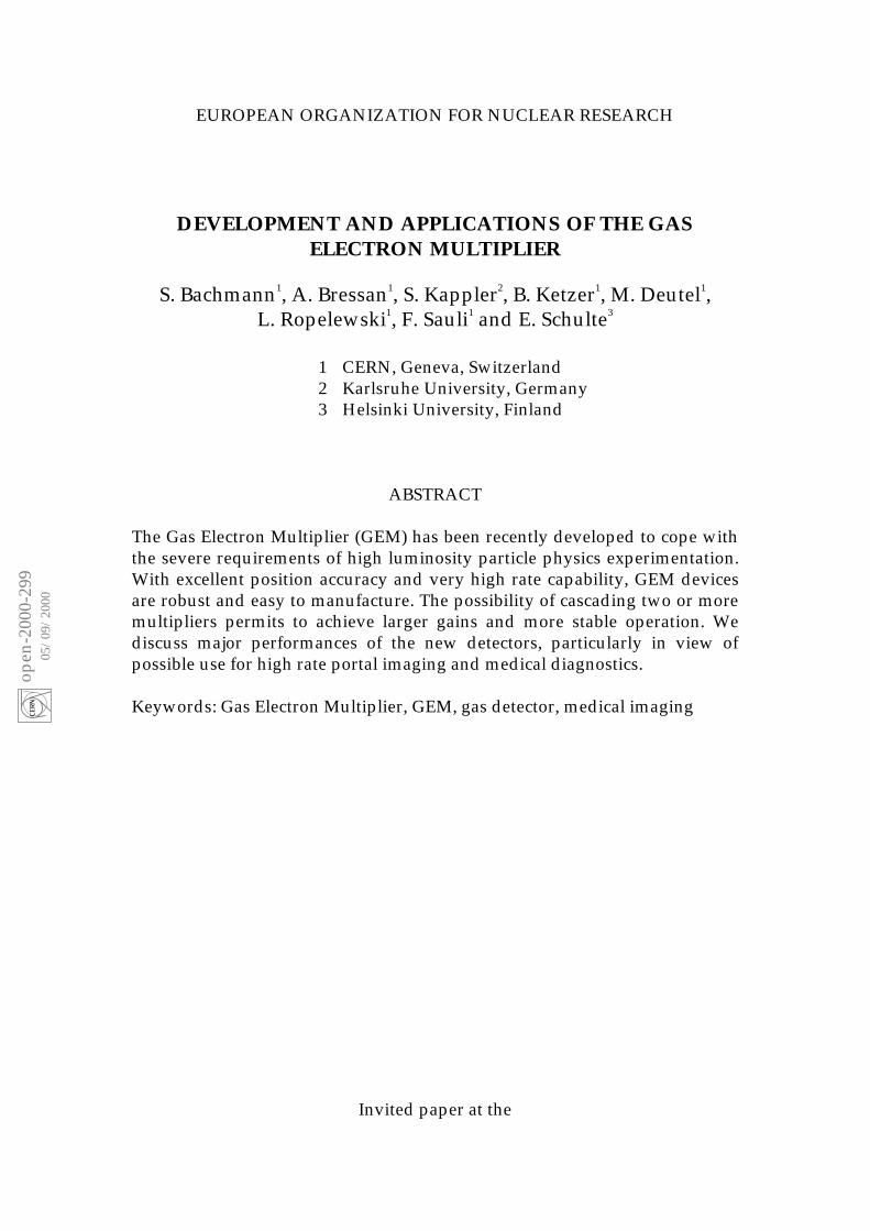
EUROPEAN ORGANIZATION FOR NUCLEAR RESEARCH
DEVELOPMENT AND APPLICATIONS OF THE GASELECTRON MULTIPLIER
S. Bachmann1, A. Bressan1, S. Kappler2, B. Ketzer1, M. Deutel1,L. Ropelewski1, F. Sauli1 and E. Schulte3
1 CERN, Geneva, Switzerland2 Karlsruhe University, Germany3 Helsinki University, Finland
ABSTRACT
The Gas Electron Multiplier (GEM) has been recently developed to cope withthe severe requirements of high luminosity particle physics experimentation.With excellent position accuracy and very high rate capability, GEM devicesare robust and easy to manufacture. The possibility of cascading two or moremultipliers permits to achieve larger gains and more stable operation. Wediscuss major performances of the new detectors, particularly in view ofpossible use for high rate portal imaging and medical diagnostics.
Keywords: Gas Electron Multiplier, GEM, gas detector, medical imaging
Invited paper at the
open
-200
0-29
905
/09
/20
00

Imaging 2000 conferenceStockholm, Sweden, June 28-July 1, 2000
Corresponding author: [email protected]
1
1. Introduction
Following the innovative invention of the micro-strip gas chamber (MSGC[1]), a variety of performing gaseous devices, collectively named micro-pattern detectors (MPD), has been developed in the recent years [2].Providing good detection efficiency and localization accuracy at high rates,they are successfully used in high energy physics experiments and otherapplied fields. Recent experience has shown however that MPDs have atendency to discharge when exposed to high rates or to highly ionizingparticles [3-5]. The appearance of discharges is attributed to the avalanchesize exceeding a critical value, in the range 107-108, the so-called Raether limit.At this point, a transition from proportional avalanche to streamer may occur,often followed by a rupture of the gas dielectric rigidity. With the exception ofthe MSGC, the new MPD devices are generally sturdy enough to withstanddischarges without damages. This may not be the case however for thesensitive readout electronics; moreover, the recovery time after a breakdowncan seriously affects the detector efficiency.
2. The gas electron multiplier
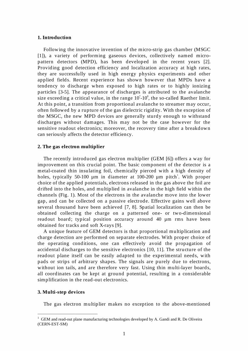
The recently introduced gas electron multiplier (GEM [6]) offers a way forimprovement on this crucial point. The basic component of the detector is ametal-coated thin insulating foil, chemically pierced with a high density ofholes, typically 50-100 µm in diameter at 100-200 µm pitch1. With properchoice of the applied potentials, electrons released in the gas above the foil aredrifted into the holes, and multiplied in avalanche in the high field within thechannels (Fig. 1). Most of the electrons in the avalanche move into the lowergap, and can be collected on a passive electrode. Effective gains well aboveseveral thousand have been achieved [7, 8]. Spatial localization can then beobtained collecting the charge on a patterned one- or two-dimensionalreadout board; typical position accuracy around 40 µm rms have beenobtained for tracks and soft X-rays [9].
A unique feature of GEM detectors is that proportional multiplication andcharge detection are performed on separate electrodes. With proper choice ofthe operating conditions, one can effectively avoid the propagation ofaccidental discharges to the sensitive electronics [10, 11]. The structure of thereadout plane itself can be easily adapted to the experimental needs, withpads or strips of arbitrary shapes. The signals are purely due to electrons,without ion tails, and are therefore very fast. Using thin multi-layer boards,all coordinates can be kept at ground potential, resulting in a considerablesimplification in the read-out electronics.
3. Multi-step devices
The gas electron multiplier makes no exception to the above-mentioned
1 GEM and read-out plane manufacturing technologies developed by A. Gandi and R. De Oliveira(CERN-EST-SM)
2
appearance of discharges at high rates or in presence of heavily ionizingtacks. A solution to this fundamental problem has been found however, bycascading several multiplying elements, an approach developed long ago inthe so-called multi-step chamber [12]. This can be easily achieved with aGEM, used as pre-amplifier in combination with another MPD. The exactreasons for the improvement are not completely clear. It is suspected that,since in cascaded system the same overall gain is obtained with each elementoperated at reduced voltage, the amount of charge required for the transitionis larger. In other words, the Raether limit might be voltage dependent.Alternatively, one can invoke the larger avalanche spread in multiplestructures to reduce the charge density [4]. A two-stage detector made with aGEM in front of a MSGC permits to reach an order of magnitude higher gainsbefore discharges [7, 13]. This is the solution adopted for the tracker of HERA-B experiment, originally based on the MSGC technology and has led to thefirst large production of GEM electrodes. More than two hundred foils, 27x25cm2 each, have been manufactured and are being integrated in theexperimental set-up at DESY [14].
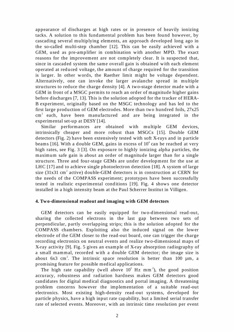
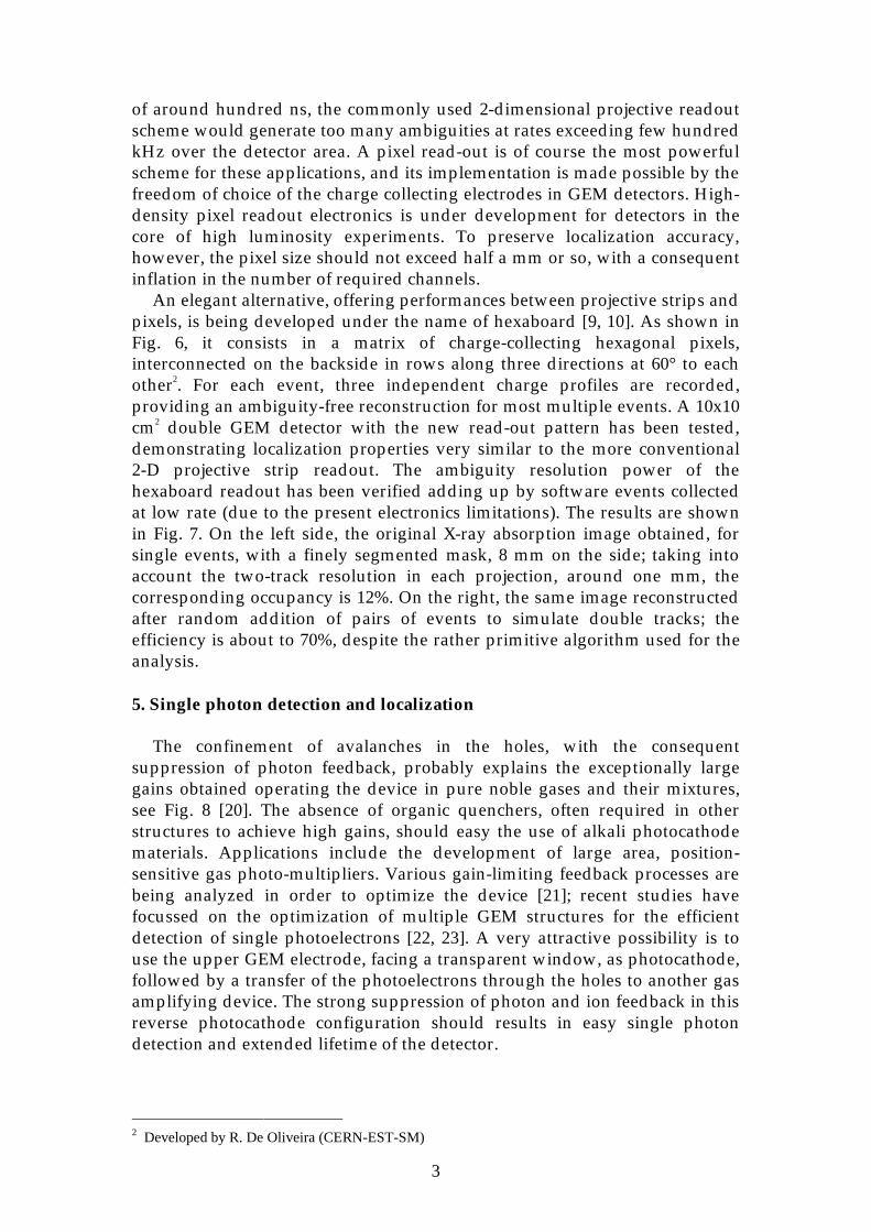
Similar performances are obtained with multiple GEM devices,intrinsically cheaper and more robust than MSGCs [15]. Double GEMdetectors (Fig. 2) have been extensively tested with soft X-rays and in particlebeams [16]. With a double GEM, gains in excess of 104 can be reached at veryhigh rates, see Fig. 3 [3]. On exposure to highly ionizing alpha particles, themaximum safe gain is about an order of magnitude larger than for a singlestructure. Three and four-stage GEMs are under development for the use atLHC [17] and to achieve single photoelectron detection [18]. A system of largesize (31x31 cm2 active) double-GEM detectors is in construction at CERN forthe needs of the COMPASS experiment; prototypes have been successfullytested in realistic experimental conditions [19]. Fig. 4 shows one detectorinstalled in a high intensity beam at the Paul Scherrer Institut in Villigen.
4. Two-dimensional readout and imaging with GEM detectors
GEM detectors can be easily equipped for two-dimensional read-out,sharing the collected electrons in the last gap between two sets ofperpendicular, partly overlapping strips; this is the solution adopted for theCOMPASS chambers. Exploiting also the induced signal on the lowerelectrode of the GEM closer to the read-out board, one can trigger the chargerecording electronics on neutral events and realize two-dimensional maps ofX-ray activity [9]. Fig. 5 gives an example of X-ray absorption radiography ofa small mammal, recorded with a double GEM detector; the image size isabout 6x3 cm2. The intrinsic space resolution is better than 100 µm, apromising feature for possible medical applications.
The high rate capability (well above 105 Hz mm-2), the good positionaccuracy, robustness and radiation hardness makes GEM detectors goodcandidates for digital medical diagnostics and portal imaging. A threateningproblem concerns however the implementation of a suitable read-outelectronics. Most existing high-density read-out systems, developed forparticle physics, have a high input rate capability, but a limited serial transferrate of selected events. Moreover, with an intrinsic time resolution per event
3
of around hundred ns, the commonly used 2-dimensional projective readoutscheme would generate too many ambiguities at rates exceeding few hundredkHz over the detector area. A pixel read-out is of course the most powerfulscheme for these applications, and its implementation is made possible by thefreedom of choice of the charge collecting electrodes in GEM detectors. High-density pixel readout electronics is under development for detectors in thecore of high luminosity experiments. To preserve localization accuracy,however, the pixel size should not exceed half a mm or so, with a consequentinflation in the number of required channels.
An elegant alternative, offering performances between projective strips andpixels, is being developed under the name of hexaboard [9, 10]. As shown inFig. 6, it consists in a matrix of charge-collecting hexagonal pixels,interconnected on the backside in rows along three directions at 60° to eachother2. For each event, three independent charge profiles are recorded,providing an ambiguity-free reconstruction for most multiple events. A 10x10cm2 double GEM detector with the new read-out pattern has been tested,demonstrating localization properties very similar to the more conventional2-D projective strip readout. The ambiguity resolution power of thehexaboard readout has been verified adding up by software events collectedat low rate (due to the present electronics limitations). The results are shownin Fig. 7. On the left side, the original X-ray absorption image obtained, forsingle events, with a finely segmented mask, 8 mm on the side; taking intoaccount the two-track resolution in each projection, around one mm, thecorresponding occupancy is 12%. On the right, the same image reconstructedafter random addition of pairs of events to simulate double tracks; theefficiency is about to 70%, despite the rather primitive algorithm used for theanalysis.
5. Single photon detection and localization
The confinement of avalanches in the holes, with the consequentsuppression of photon feedback, probably explains the exceptionally largegains obtained operating the device in pure noble gases and their mixtures,see Fig. 8 [20]. The absence of organic quenchers, often required in otherstructures to achieve high gains, should easy the use of alkali photocathodematerials. Applications include the development of large area, position-sensitive gas photo-multipliers. Various gain-limiting feedback processes arebeing analyzed in order to optimize the device [21]; recent studies havefocussed on the optimization of multiple GEM structures for the efficientdetection of single photoelectrons [22, 23]. A very attractive possibility is touse the upper GEM electrode, facing a transparent window, as photocathode,followed by a transfer of the photoelectrons through the holes to another gasamplifying device. The strong suppression of photon and ion feedback in thisreverse photocathode configuration should results in easy single photondetection and extended lifetime of the detector.
2 Developed by R. De Oliveira (CERN-EST-SM)

4
The part of this work describing the imaging performances of GEM hasgreatly profited from continuing support and interest of the group led byProf. T. Müller (Inst. Experimentelle Kernphysik, Universität Karlsruhe).
5
REFERENCES
[1] A. Oed, Nucl. Instrum. and Meth. A263 (1988) 351.[2] F. Sauli and A. Sharma, Ann. Rev. Nucl. Part. Sci. 49 (1999) 341.[3] A. Bressan, M. Hoch, P. Pagano, L. Ropelewski, F. Sauli, S. Biagi, A.
Buzulutskov, M. Gruwé, A. Sharma, D. Moermann, G. De Lentdecker,Nucl. Instrum. and Meth. A424 (1998) 321.
[4] V. Peskov, B.D. Ramsey, P. Fonte, IEEE Trans. Nucl. Sci. NS-45 (1998) 244.[5] P. Fonte, V. Peskov, B.D. Ramsey, Nucl. Instrum. and Meth. A 419 (1998)
405.[6] F. Sauli, Nucl. Instrum. and Meth. A386 (1997) 531.[7] R. Bouclier, W. Dominik, M. Hoch, J.C. Labbé, G. Million, L. Ropelewski,
F. Sauli, A. Sharma, G. Manzin, Nucl. Instrum. and Meth. A396 (1997) 50.[8] J. Benlloch, A. Bressan, M. Capeáns, M. Gruwé, M. Hoch, J.C. Labbé, A.
Placci, L. Ropelewski, F. Sauli, Nucl. Instrum. and Meth. A 419 (1998) 410.[9] A. Bressan, L. Ropelewski, F. Sauli, D. Mörmann, T. Müller, H.J. Simonis,
Nucl. Instrum. and Meth. A425 (1999) 254.[10]F. Sauli, Gas detectors: achievements and trends, 8th Pisa Meeting on
Advanced Detectors (Isola d'Elba, Italy, 21-27 May 2000). CERN-EP/2000-080. Subm. Nucl. Instrum. Methods (2000).
[11]S. Bachmann, A. Bressan, M. Deutel, S. Kappler, B. Ketzer, A. Polouektov,L. Ropelewski, F. Sauli, E. Schulte, L. Shekhtman, A. Sokolov, Dischargemechanisms and prevention in the gas electron multiplier, Subm. Nucl.Instrum. Methods (2000).
[12]G. Charpak and F. Sauli, Phys. Letters 78 B (1978) 523.[13]Y. Benhammou, R. Blaes, J.M. Brom, F. Drouhin, J.C. Fontaine, D. Huss, F.
Jeanneau, V. Mack, I. Ripp-Baudot, B. Schwaller, A. Zghiche, Nucl.Instrum. Methods A441 (2000) 452.
[14]T. Zeuner, Nucl. Instrum. Methods A 446 (2000) 324.[15]C. Büttner, M. Capeáns, W. Dominik, M. Hoch, J.C. Labbé, G. Manzin, G.
Million, L. Ropelewski, F. Sauli, A. Sharma, Nucl. Instrum. and Meth. A409 (1998) 79.
[16]A. Bressan, J.C. Labbé, P. Pagano, L. Ropelewski, F. Sauli, Nucl. Instrum.and Meth. A425 (1999) 262.
[17]M. Ziegler, P. Cwetanski, U. Straumann, A triple GEM detector for LHCb,LHCb TRAC 99-024 (1999).
[18]G. Garty, R. Chechik, A. Breskin, E. Shefer, Nucl. Instrum. and Meth.A433 (1999) 476.
[19]S. Bachmann, A. Bressan, A. Placci, L. Ropelewski, F. Sauli, IEEE Trans.Nucl. Sci. NS-47 (2000) .
[20]A. Buzulutskov, A. Breskin, R. Chechik, G. Garty, F. Sauli, L. Shekhtman,Nucl. Instrum. Methods A 443 (2000) 164.
[21]A. Breskin, T. Boutboul, A. Buzulutskov, R. Chechik, G. Garty, E. Shefer,B.K. Singh, Nucl. Instrum. Methods A 442 (2000) 58.
[22]A. Sharma, Detection of single electrons emitted by internalphotocathodes with the gas electron multiplier (GEM), CERN-OPEN-99/372. Subm. Nucl. Instrum. Methods (1999).

6
[23]C. Richter, A. Breskin, R. Chechik, G. Garty, A. Sharma, Single electrontransfer efficiency of GEM, 8th Pisa Meeting on Advanced Detectors(Isola d’Elba, Italy, 21-27 May 2000). Subm. Nucl. Instrum. Methods(2000).
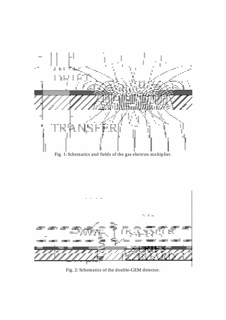
Fig. 1: Schematics and fields of the gas electron multiplier.
Fig. 2: Schematics of the double-GEM detector.

Fig. 3: Current in the double-GEM detector as a function of voltage in oneGEM, for increasing X-ray flux. The gain can be read on the lower curve.
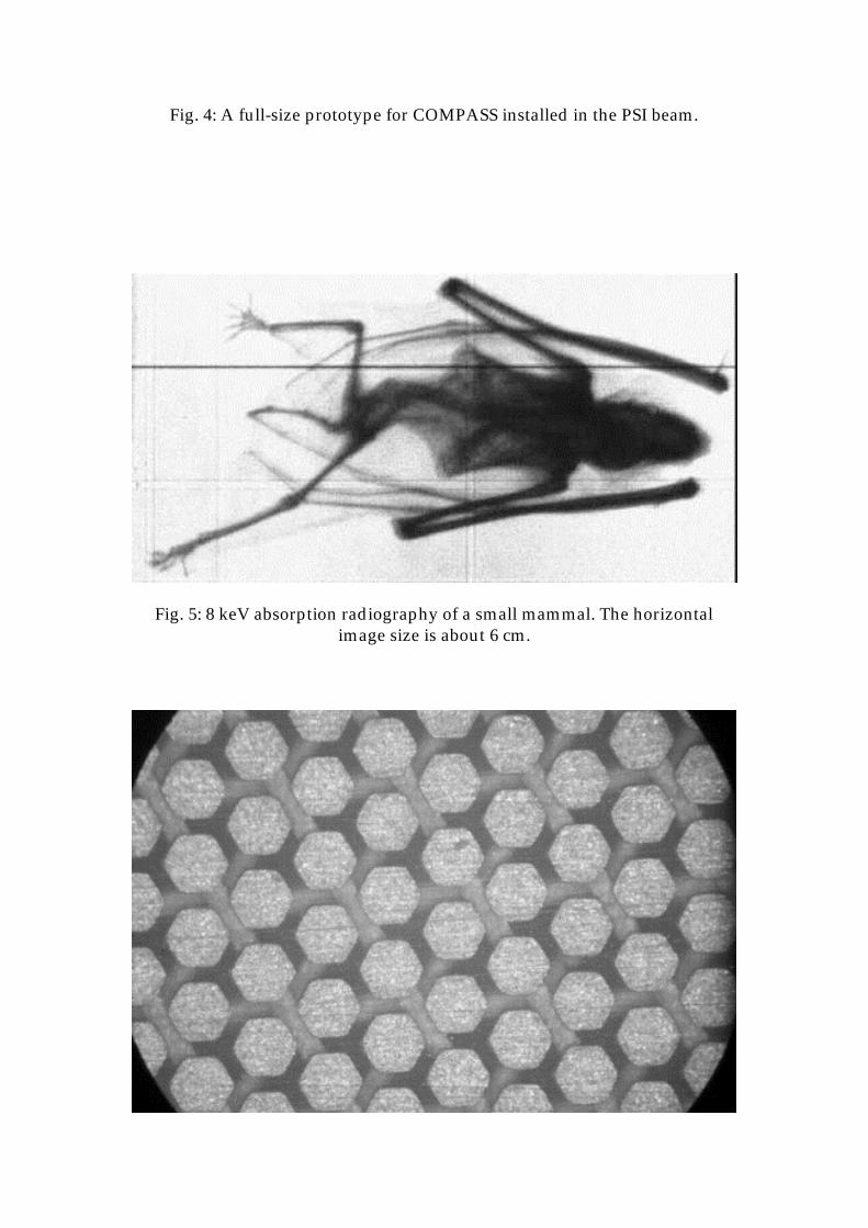
Fig. 4: A full-size prototype for COMPASS installed in the PSI beam.
Fig. 5: 8 keV absorption radiography of a small mammal. The horizontalimage size is about 6 cm.
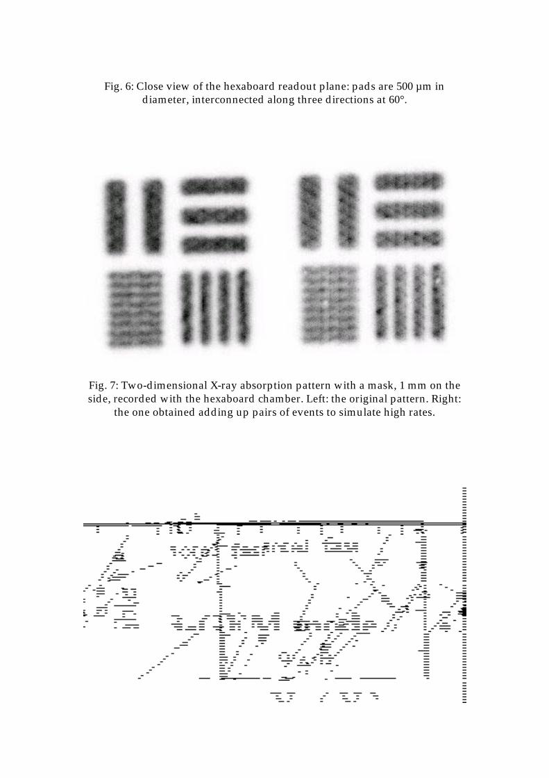
Fig. 6: Close view of the hexaboard readout plane: pads are 500 µm indiameter, interconnected along three directions at 60°.
Fig. 7: Two-dimensional X-ray absorption pattern with a mask, 1 mm on theside, recorded with the hexaboard chamber. Left: the original pattern. Right:
the one obtained adding up pairs of events to simulate high rates.
Fig. 8: Large gains obtained with triple-GEM structure in various noble gasmixtures.