Embed Size (px)
Citation preview
IPN Progress Report 42-147 November 15, 2001
Developing Low-Power Transceiver Technologies forIn Situ Communication Applications
N. Lay,1 C. Cheetham,1 H. Mojaradi,1 and J. Neal1
For future deep-space missions, significant reductions in the mass and power re-quirements for short-range telecommunication systems will be critical in enablinga wide variety of new mission concepts. These possibilities include penetrators,gliders, miniature rovers, balloons, and sensor networks. The recent develop-ment activity reported in this article has focused on the design of ultra-low-massand -power transceiver systems and subsystems suitable for operation in a flight en-vironment. Under these efforts, the basic functionality of the transceiver has beentargeted towards a Mars microprobe communications scenario. However, the over-all transceiver architecture is well suited to any short- or medium-range applicationwhere a remote probe will aperiodically communicate with a base station, possiblyan orbiter, for the eventual purpose of relaying science information back to Earth.Additionally, elements of the radio architecture can be applied in situations in-volving surface-to-surface communications, thereby enabling different mission com-munications topologies. Through a system analysis of these channels, both theapplicability and benefit of very low power communications will be quantitativelyaddressed.
I. Introduction
The development of telecommunications equipment emphasizing very low power consumption andmass will be a significant enabler of future in situ missions with highly constrained payload resources.The activities reported in this article began as a follow-on and complementary effort of the Micro Com-munications and Avionics Systems first prototype (MCAS1) [1]. The baseline transceiver concept, underthis effort, has been oriented towards a Mars microprobe-type mission that would deploy to the surface,gather science, and await opportunities for return-link data transmissions to a low-altitude polar orbiter,as shown in Fig. 1. It is envisioned that such a mission would be characterized by communications toan orbiting satellite with local relay capability, where the communications duration and frequency wouldbe driven by return-link opportunities coupled with science data collection requirements. Under such ascenario, receiver power consumption is a critical parameter in determining mission duration, and anysignificant improvements in this arena will have a direct benefit on the mission’s longevity. Consequently,a principal focus of the development activity has been to design and demonstrate a low-complexity, low-
1 Communications Systems and Research Section.
The research described in this publication was carried out by the Jet Propulsion Laboratory, California Institute ofTechnology, under a contract with the National Aeronautics and Space Administration.
1
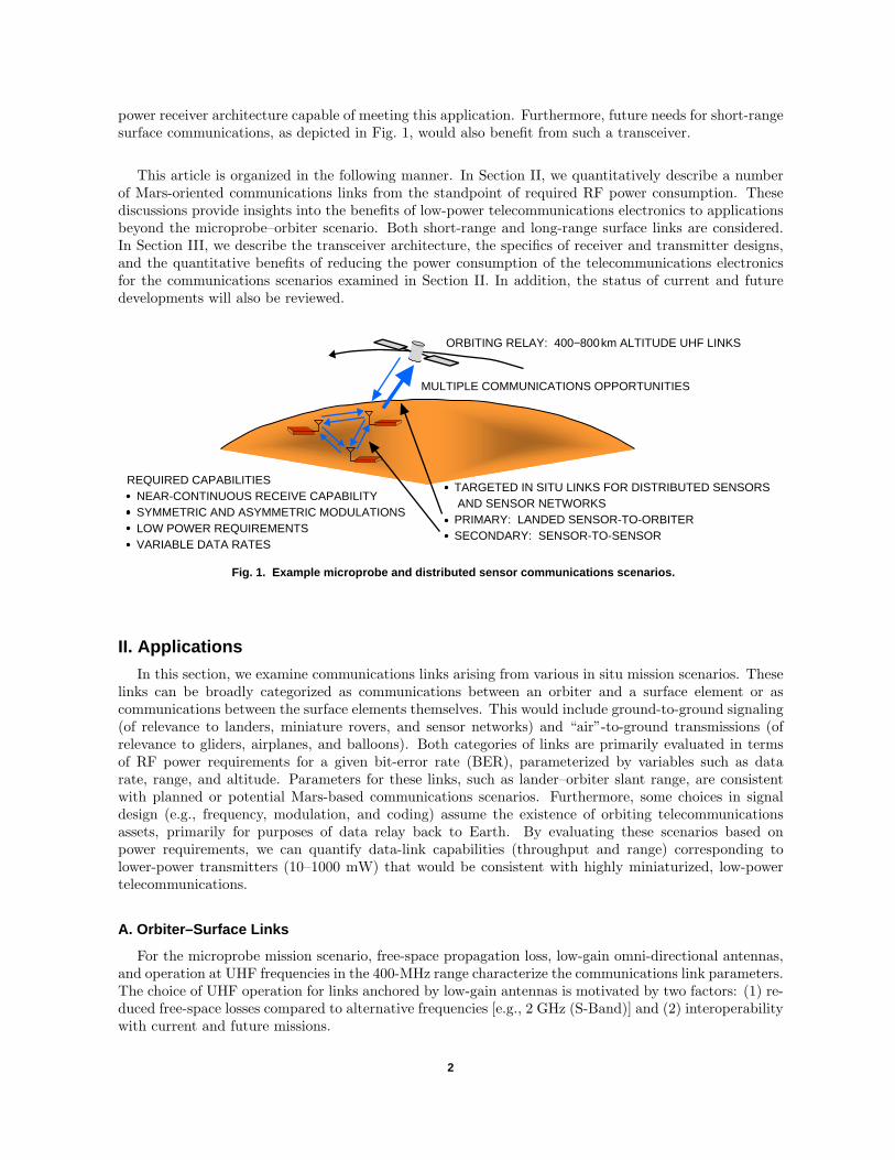
power receiver architecture capable of meeting this application. Furthermore, future needs for short-rangesurface communications, as depicted in Fig. 1, would also benefit from such a transceiver.
This article is organized in the following manner. In Section II, we quantitatively describe a numberof Mars-oriented communications links from the standpoint of required RF power consumption. Thesediscussions provide insights into the benefits of low-power telecommunications electronics to applicationsbeyond the microprobe–orbiter scenario. Both short-range and long-range surface links are considered.In Section III, we describe the transceiver architecture, the specifics of receiver and transmitter designs,and the quantitative benefits of reducing the power consumption of the telecommunications electronicsfor the communications scenarios examined in Section II. In addition, the status of current and futuredevelopments will also be reviewed.
ORBITING RELAY: 400−800 km ALTITUDE UHF LINKS
REQUIRED CAPABILITIES NEAR-CONTINUOUS RECEIVE CAPABILITY SYMMETRIC AND ASYMMETRIC MODULATIONS LOW POWER REQUIREMENTS VARIABLE DATA RATES
Fig. 1. Example microprobe and distributed sensor communications scenarios.
MULTIPLE COMMUNICATIONS OPPORTUNITIES
TARGETED IN SITU LINKS FOR DISTRIBUTED SENSORS AND SENSOR NETWORKS PRIMARY: LANDED SENSOR-TO-ORBITER SECONDARY: SENSOR-TO-SENSOR
II. Applications
In this section, we examine communications links arising from various in situ mission scenarios. Theselinks can be broadly categorized as communications between an orbiter and a surface element or ascommunications between the surface elements themselves. This would include ground-to-ground signaling(of relevance to landers, miniature rovers, and sensor networks) and “air”-to-ground transmissions (ofrelevance to gliders, airplanes, and balloons). Both categories of links are primarily evaluated in termsof RF power requirements for a given bit-error rate (BER), parameterized by variables such as datarate, range, and altitude. Parameters for these links, such as lander–orbiter slant range, are consistentwith planned or potential Mars-based communications scenarios. Furthermore, some choices in signaldesign (e.g., frequency, modulation, and coding) assume the existence of orbiting telecommunicationsassets, primarily for purposes of data relay back to Earth. By evaluating these scenarios based onpower requirements, we can quantify data-link capabilities (throughput and range) corresponding tolower-power transmitters (10–1000 mW) that would be consistent with highly miniaturized, low-powertelecommunications.
A. Orbiter–Surface Links
For the microprobe mission scenario, free-space propagation loss, low-gain omni-directional antennas,and operation at UHF frequencies in the 400-MHz range characterize the communications link parameters.The choice of UHF operation for links anchored by low-gain antennas is motivated by two factors: (1) re-duced free-space losses compared to alternative frequencies [e.g., 2 GHz (S-Band)] and (2) interoperabilitywith current and future missions.
2

Tables 1 and 2, respectively, provide example link budget details for forward- and return-link communi-cations between a low-altitude polar-orbiting relay and a landed surface probe. The format and numerousparameter values, such as link frequencies, nominal losses, equivalent temperature, noise figure, etc., havebeen summarized from more detailed versions taken from various sources.2,3 The communications range
Table 1. Orbit-to-surface command/hailing link budget.
Parameter Value
Orbiter transmitter
Transmitter power 30 dBm
Transmitter circuit losses −1.0 dB
Antenna gain 0.0 dB
Link
Range 894.3 km
Link frequency 437.1 MHz
Space losses −144.28 dB
Microprobe receiver
Antenna gain 0.0 dB
Polarization losses −0.2 dB
Receiver circuit losses −1.0 dB
Receiver noise figure 3.0 dB
System noise temperature 600 K
Noise spectral density −170.9 dBm/Hz
Total power summary
Received power −116.48 dBm
Received C/No 54.42 dB
Data-channel performance
Data bit rate 1000 b/s
Eb/No to receiver 24.42 dB
Implementation loss 2.0 dB
Effective Eb/No 22.42 dB
Uncoded BPSK performance margin 11.82 dB
Uncoded DPSK performance margin 11.62 dB
Uncoded FSK performance margin 8.22 dB
2 D. Hansen, MCAS1 Functional Requirements, draft (JPL internal document), Jet Propulsion Laboratory, Pasadena,California, October 1999.
3 D. Hansen and M. Sue, Frequency Bands for Local Communication and Navigation in the Mars Region, (JPL internaldocument), Jet Propulsion Laboratory, Pasadena, California, January 31, 2001.
3

Table 2. Surface-to-orbit link budget.
Parameter Value
Microprobe transmitter
Transmitter power 26 dBm
Transmitter circuit losses −1.0 dB
Antenna gain 0.0 dB
Link
Range 894.3 km
Link frequency 401.5 MHz
Space losses −143.55 dB
Orbiter receiver
Antenna gain 0.0 dB
Polarization losses −0.2 dB
Receiver circuit losses −1.0 dB
Receiver noise figure 3.0 dB
System noise temperature 600 K
Noise spectral density −170.9 dBm/Hz
Total power summary
Received power −119.75 dBm
Received C/No 51.15 dB
Data-channel performance
Data bit rate 20,000 b/s
Eb/No to receiver 8.14 dB
Implementation loss 1.5 dB
Effective Eb/No 6.64 dB
(7,1/2) convolutionally coded BPSK 2.04 dBperformance margin
(2048,1024) turbo-coded BPSK 4.14 dBperformance margin
selected in these tables corresponds to the slant path for a 400-km altitude, polar-orbiting satellite situatedat an effective elevation angle of 20 deg relative to the surface transceiver. As a point of reference, thetheoretical additive white Gaussian noise (AWGN) Eb/N0 thresholds, corresponding to a BER of 10−6,for possible forward- and return-link modulation and coding choices are presented in Table 3 [2,3].
A representative forward-link data rate of 1000 b/s is shown and assumed sufficient for the pur-pose of having an orbiter individually alert multiple landed elements of return-link opportunities during asingle pass. In addition, the forward link may also be employed to deliver operational or science-gathering
4
Table 3. Ideal Eb /No thresholds for various types ofmodulation and coding, BER = 10 –6.
Required Eb/No,Modulation and coding
dB
Uncoded coherent BPSK 10.6
Uncoded non-coherent FSK 14.2
Uncoded differentially coherent BPSK 10.8
Coherent BPSK with (7,1/2) convolutional code 4.6
Coherent BPSK with (2048,1024) turbo code 2.5
commands to these elements. Transmitter RF power for the forward link is nominally set to 1 W,4
with the assumption that this could be readily increased for most orbital payloads. The command-linkmargins are given for three different uncoded modulation and detection types—coherent binary phase-shiftkeying (BPSK), differentially coherent binary phase-shift keying (DPSK), and non-coherent frequency-shift keying (FSK). Uncoded modulations are selected on the forward link to minimize microprobe receivercomplexity. Based on the moderately large margins shown in Table 1, the use of forward error correction(FEC) would indeed not be required to close the command link for this specific scenario, and somemeasure of receiver implementation loss could be incurred if it resulted in reduced power consumption.Furthermore, even holding the margin constant, increased range could also be achieved through data-ratereductions. The actual choice of modulation can then be made on the basis of simplifying the receiverand reducing its power consumption as well as taking into consideration what forward-link signals willbe supported by current and future orbiter missions. Reductions in receiver power consumption directlytranslate to improved mission longevity when the experiment configuration calls for semi-continuous5
operation to await random access commands from an orbiter.
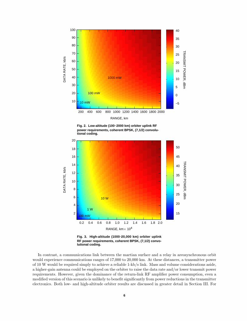
A transmitter output power of 400 mW and data rate of 20 kb/s are used in the return-link exampleof Table 2 and are shown to be sufficient for reliable communications given the use of either the (7,1/2)convolutional code or rate-1/2, 1024-bit block turbo code. The use of FEC on this link is stronglywarranted in order to reduce the output power amplifier requirements as much as possible. To determineif reduced power consumption in transmitter electronics (exclusive of the RF power amplifier) can impactoverall savings, we will expand upon the results of Table 2 by parametrically calculating transmitter powerrequirements. This is achieved by fixing the (7,1/2) convolutional code and then varying the return-linkdata rate and the slant-path range to generate the corresponding transmit RF signal powers for a 3-dBmargin. These results are respectively and compactly shown in Figs. 2 and 3 for slant ranges correspondingto low-altitude (polar-orbiting) and high-altitude (areostationary) telecommunications relay links. InFig. 2, the data rates span 1–100 kb/s, and the link distance ranges from 100 to 2000 km. The color barshown on the right-hand side of the figure describes the quantitative mapping between transmitter power(dBm) and the plotted color contours. From these results, we note that transmitter powers under 1 Wwill be able to support 100-kb/s data rates over much of a 400-km-altitude relay’s orbit6 and will support40 kb/s over the relay’s full orbit.7 Note that these plots do not consider elevation-angle-based antennagain dependencies. In practice, extreme slant ranges for a given orbit will require somewhat more powerdue to low horizon gain for the surface element’s antenna.
4 Comparable to the 1.3-W UHF forward link on Mars Global Surveyor.
5 It is assumed that commonly used power-reduction techniques such as low duty cycle operation will also be applied.
6 Defined as elevation angles greater than 30-deg elevation and less than 700-km range.
7 Defined as elevation angles greater than 20-deg elevation and less than 900-km range.
5
200
1000 mW
400 600 800 1000 1200 1400 1600 1800 2000
RANGE, km
10
20
30
40
50
60
70
80
90
100
10 mW
100 mW
DA
TA
RA
TE
, kb/
sT
RA
NS
MIT
PO
WE
R, dB
m
40
35
30
25
20
15
10
5
0
−5
Fig. 2. Low-altitude (100−2000 km) orbiter uplink RFpower requirements, coherent BPSK, (7,1/2) convolu-tional coding.
0.2 0.4 0.6 0.8 1.0 1.2 1.4 1.6 1.8 2.0
RANGE, km 104
2
4
6
8
10
12
14
16
18
20
10 W
100 mW
DA
TA
RA
TE
, kb/
sT
RA
NS
MIT
PO
WE
R, dB
m
50
45
40
35
30
25
20
15
Fig. 3. High-altitude (1000−20,000 km) orbiter uplinkRF power requirements, coherent BPSK, (7,1/2) convo-lutional coding.
1 W
In contrast, a communications link between the martian surface and a relay in areosynchronous orbitwould experience communications ranges of 17,000 to 20,000 km. At these distances, a transmitter powerof 10 W would be required simply to achieve a reliable 1-kb/s link. Mass and volume considerations aside,a higher-gain antenna could be employed on the orbiter to raise the data rate and/or lower transmit powerrequirements. However, given the dominance of the return-link RF amplifier power consumption, even amodified version of this scenario is unlikely to benefit significantly from power reductions in the transmitterelectronics. Both low- and high-altitude orbiter results are discussed in greater detail in Section III. For
6
both of these figures, we are able to produce the corresponding in situ turbo code results by applying a2.1-dB reduction in required transmitter power.
B. Surface Links
For surface links, we consider two different communications scenarios corresponding to short-rangeground-to-ground and longer-range “air”-to-ground communications. The following analyses addressonly large-scale propagation models for these channels. The small-scale effects that produce stochasticallymodeled signal variability, such as shadowing and multipath fading, are not factored into these evaluations.Low-gain antennas are assumed at both the transmitter and the receiver for all surface-link channelsdiscussed.
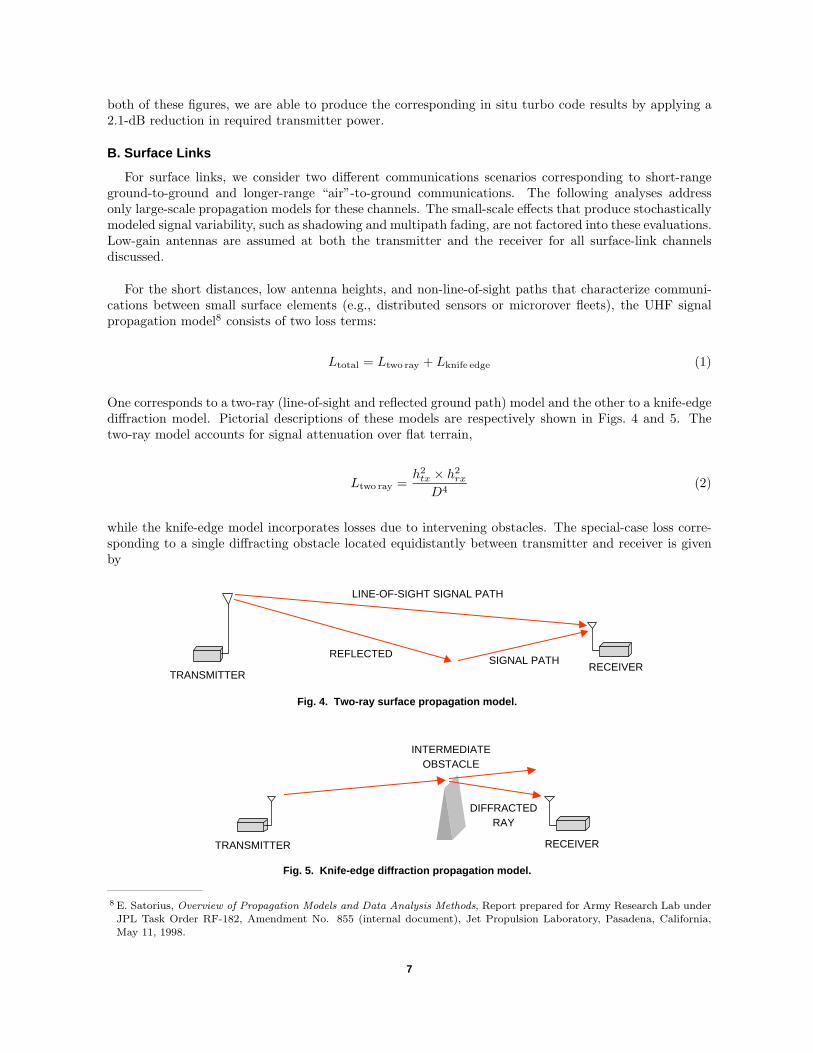
For the short distances, low antenna heights, and non-line-of-sight paths that characterize communi-cations between small surface elements (e.g., distributed sensors or microrover fleets), the UHF signalpropagation model8 consists of two loss terms:
Ltotal = Ltwo ray + Lknife edge (1)
One corresponds to a two-ray (line-of-sight and reflected ground path) model and the other to a knife-edgediffraction model. Pictorial descriptions of these models are respectively shown in Figs. 4 and 5. Thetwo-ray model accounts for signal attenuation over flat terrain,
Ltwo ray =h2tx × h2
rx
D4(2)
while the knife-edge model incorporates losses due to intervening obstacles. The special-case loss corre-sponding to a single diffracting obstacle located equidistantly between transmitter and receiver is givenby
TRANSMITTERRECEIVER
LINE-OF-SIGHT SIGNAL PATH
REFLECTEDSIGNAL PATH
Fig. 4. Two-ray surface propagation model.
TRANSMITTER RECEIVER
INTERMEDIATEOBSTACLE
DIFFRACTEDRAY
Fig. 5. Knife-edge diffraction propagation model.
8 E. Satorius, Overview of Propagation Models and Data Analysis Methods, Report prepared for Army Research Lab underJPL Task Order RF-182, Amendment No. 855 (internal document), Jet Propulsion Laboratory, Pasadena, California,May 11, 1998.
7
Lknife edge =
0, ν ≤ −1
(0.5− 0.62× ν)2, −1 < ν ≤ 0(
0.5× e−0.95ν)2, 0 < ν ≤ 1(
0.4−√
0.1184− (0.38− 0.1× ν)2)2
, 1 < ν ≤ 2.4(0.225ν
)2
, ν > 2.4
(3)
where
ν = hobstacle ×√
8λ×D
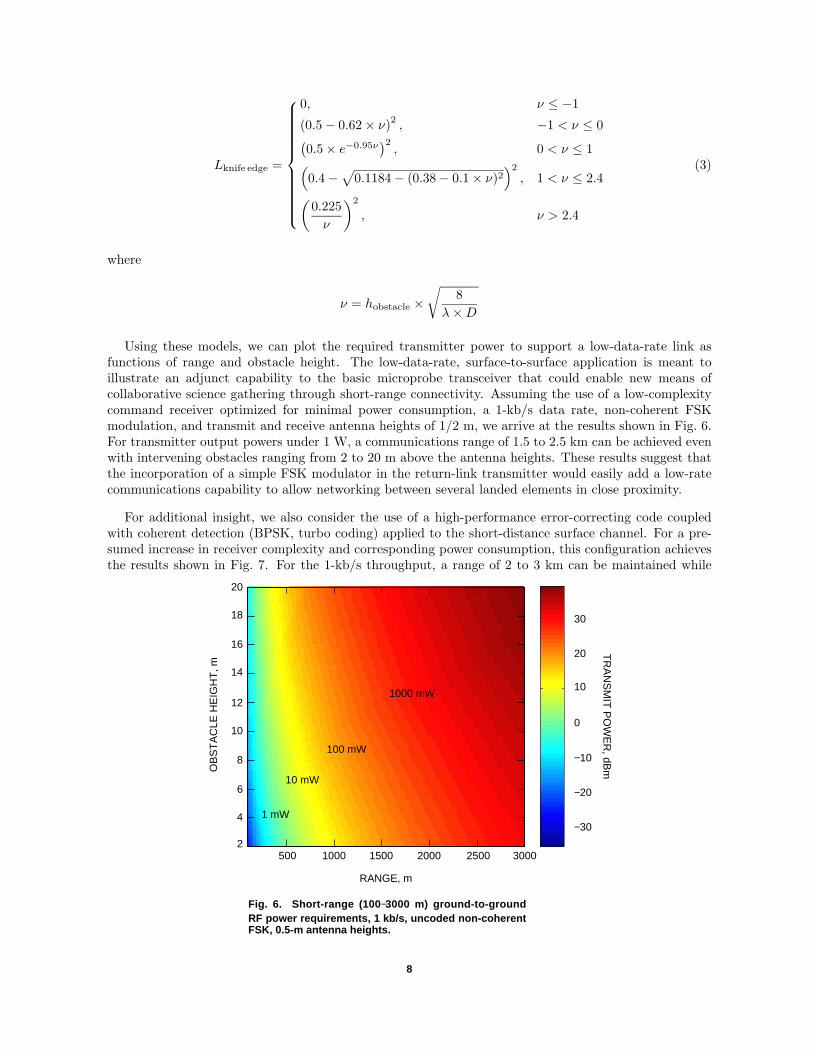
Using these models, we can plot the required transmitter power to support a low-data-rate link asfunctions of range and obstacle height. The low-data-rate, surface-to-surface application is meant toillustrate an adjunct capability to the basic microprobe transceiver that could enable new means ofcollaborative science gathering through short-range connectivity. Assuming the use of a low-complexitycommand receiver optimized for minimal power consumption, a 1-kb/s data rate, non-coherent FSKmodulation, and transmit and receive antenna heights of 1/2 m, we arrive at the results shown in Fig. 6.For transmitter output powers under 1 W, a communications range of 1.5 to 2.5 km can be achieved evenwith intervening obstacles ranging from 2 to 20 m above the antenna heights. These results suggest thatthe incorporation of a simple FSK modulator in the return-link transmitter would easily add a low-ratecommunications capability to allow networking between several landed elements in close proximity.
For additional insight, we also consider the use of a high-performance error-correcting code coupledwith coherent detection (BPSK, turbo coding) applied to the short-distance surface channel. For a pre-sumed increase in receiver complexity and corresponding power consumption, this configuration achievesthe results shown in Fig. 7. For the 1-kb/s throughput, a range of 2 to 3 km can be maintained while
500 1000 3000
RANGE, m
2
4
6
8
10
12
14
16
18
20
10 mW
1 mW
OB
ST
AC
LE H
EIG
HT
, mT
RA
NS
MIT
PO
WE
R, dB
m
30
20
10
0
−10
Fig. 6. Short-range (100−3000 m) ground-to-groundRF power requirements, 1 kb/s, uncoded non-coherentFSK, 0.5-m antenna heights.
100 mW
1000 mW
1500 2000 2500
−20
−30
8

500 1000 3000
RANGE, m
2
4
6
10
12
14
16
18
20
10 mW
1 mWOB
ST
AC
LE H
EIG
HT
, mT
RA
NS
MIT
PO
WE
R, dB
m
30
20
10
0
−10
Fig. 7. Short-range (100−3000 m) ground-to-groundRF power requirements, 1 kb/s, turbo-coded coherentBPSK, 0.5-m antenna heights.
100 mW
1000 mW
1500 2000 2500
−20
−30
8
expending less than 100 mW of transmitter output power. Such a significant relative improvementcould be exploited in a ground communications scenario with a higher power consumption relay terminalconfigured as the central point of a star network topology in much the same role the orbiter assumes inrelation to surface-based microprobes.
Next, we consider the RF transmit power requirements for high-data-rate, “airborne” transmitter-to-surface communications channels. This scenario will be highly relevant to missions involving communi-cations from an elevated platform (e.g., glider, powered aircraft, balloon, etc.) to a ground-based relay.The high-data-rate application will be particularly suited to imager-based science measurements, and theground-based relay can serve as a hub for multiple long-range missions without suffering the inconstancyof a link to an orbiter. Under this configuration, we are interested in minimizing the power consumptionon the transmitter side, as these platforms will likely exhibit severe payload power, mass, and volumeconstraints. Such a focus will naturally argue for the use of FEC and coherent detection, which willconsequently impose additional complexity on the ground-based relay.
For these calculations, the gross propagation losses are modeled as a combination of square-law free-space losses and fourth-power ground-wave models where the individual loss functions are
Lfree space (D) =(
λ
4πD
)2
Ltwo ray (D) =h2tx × h2
rx
D4
(4)
The crossover point between these two expressions can be determined by setting the two functions equaland solving for the range:9
9 E. Satorius, personal communication, Jet Propulsion Laboratory, Pasadena, California, May 4, 2001.
9

Lfree space = Ltwo ray ⇒ Dcrossover =4π × htx × hrx
λ(5a)
therefore,
Lchannel ={Lfree space (D) , D ≤ Dcrossover
Lfree space (Dcrossover)× Ltwo ray (D −Dcrossover) , D > Dcrossover(5b)
For example, given transmitter altitudes of 2 and 5 km, a receiver antenna height of 1 m, and a 400-MHzcarrier frequency, the crossover point occurs at 33.5 and 83.4 km, respectively, from the transmitter. Itshould, however, be noted that these results were computed assuming a purely flat Mars surface modeland at large slant ranges will be optimistic in comparison with a model that accounts for planet curvature.
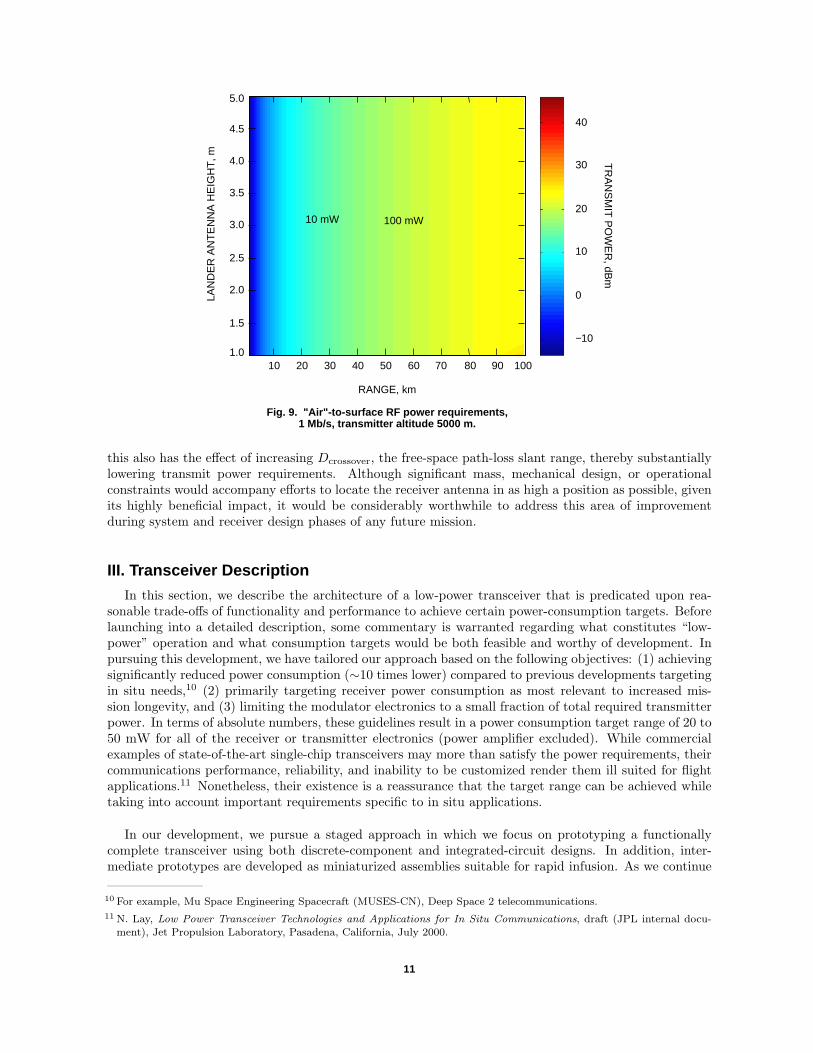
In Figs. 8 and 9, the required transmitter power is plotted as a function of range and received antennaheight for transmitter altitudes of 2 and 5 km, with convolutionally coded (7,1/2) BPSK and a data rateof 1 Mb/s. Received antenna heights are allowed to vary from 1 to 5 m, and the slant path ranges up to100 km.
Over much of the parameter space of Fig. 8 (2-km transmitter altitude), the free-space path-loss func-tion dominates the overall loss equation. Only at large slant ranges and lower received antenna heights(lower right portion of the figure) does the increased transmitter power requirement exhibit the two-rayloss mechanism. In this region, the RF power requirement rises to the 1-W level in order to close thelink for slant paths nearing 100 km. At the higher 5-km altitude, the free-space path-loss rule dominatesnearly all of Fig. 9, illustrating that on the order of 25–26 dBm (∼300–400 mW) is sufficient to downlinkhigh-rate telemetry over the considerable distance of 100 km, provided a certain altitude is achieved.However, several other practical factors will also impact the communications performance across such alink. Because of the low elevation angle at extreme ranges, these factors will include blockage due tolocal geography and frequency-selective multipath due to the high-data-rate transmission. Both of theseeffects can be partially mitigated by increasing the receiver antenna height—either through mechani-cal augmentation or by locating the receiver on high ground. In addition, as observed in Figs. 8 and 9,
20 40 100
RANGE, km
1.0
1.5
2.5
3.0
3.5
4.0
4.5
5.0
10 mW
LAN
DE
R A
NT
EN
NA
HE
IGH
T, m T
RA
NS
MIT
PO
WE
R, dB
m
30
20
10
0
−10
Fig. 8. "Air"-to-surface RF power requirements,1 Mb/s, transmitter altitude 2000 m.
100 mW
1000 mW
60 80 90
2.0
40
70503010
10
20 40 100
RANGE, km
1.0
1.5
2.5
3.0
3.5
4.0
4.5
5.0
10 mWLA
ND
ER
AN
TE
NN
A H
EIG
HT
, m TR
AN
SM
IT P
OW
ER
, dBm
30
20
10
0
−10
Fig. 9. "Air"-to-surface RF power requirements,1 Mb/s, transmitter altitude 5000 m.
100 mW
60 80 90
2.0
40
70503010
this also has the effect of increasing Dcrossover, the free-space path-loss slant range, thereby substantiallylowering transmit power requirements. Although significant mass, mechanical design, or operationalconstraints would accompany efforts to locate the receiver antenna in as high a position as possible, givenits highly beneficial impact, it would be considerably worthwhile to address this area of improvementduring system and receiver design phases of any future mission.
III. Transceiver Description
In this section, we describe the architecture of a low-power transceiver that is predicated upon rea-sonable trade-offs of functionality and performance to achieve certain power-consumption targets. Beforelaunching into a detailed description, some commentary is warranted regarding what constitutes “low-power” operation and what consumption targets would be both feasible and worthy of development. Inpursuing this development, we have tailored our approach based on the following objectives: (1) achievingsignificantly reduced power consumption (∼10 times lower) compared to previous developments targetingin situ needs,10 (2) primarily targeting receiver power consumption as most relevant to increased mis-sion longevity, and (3) limiting the modulator electronics to a small fraction of total required transmitterpower. In terms of absolute numbers, these guidelines result in a power consumption target range of 20 to50 mW for all of the receiver or transmitter electronics (power amplifier excluded). While commercialexamples of state-of-the-art single-chip transceivers may more than satisfy the power requirements, theircommunications performance, reliability, and inability to be customized render them ill suited for flightapplications.11 Nonetheless, their existence is a reassurance that the target range can be achieved whiletaking into account important requirements specific to in situ applications.
In our development, we pursue a staged approach in which we focus on prototyping a functionallycomplete transceiver using both discrete-component and integrated-circuit designs. In addition, inter-mediate prototypes are developed as miniaturized assemblies suitable for rapid infusion. As we continue
10 For example, Mu Space Engineering Spacecraft (MUSES-CN), Deep Space 2 telecommunications.
11 N. Lay, Low Power Transceiver Technologies and Applications for In Situ Communications, draft (JPL internal docu-ment), Jet Propulsion Laboratory, Pasadena, California, July 2000.
11
with the development, we plan to refine power and performance on a subsystem-by-subsystem basis andreplace the functional prototypes with their end products. This approach exhibits the dual virtues of po-tentially applying intermediate products to near-term missions and continually maintaining a full systemtest capability throughout the evolution of various transceiver elements.
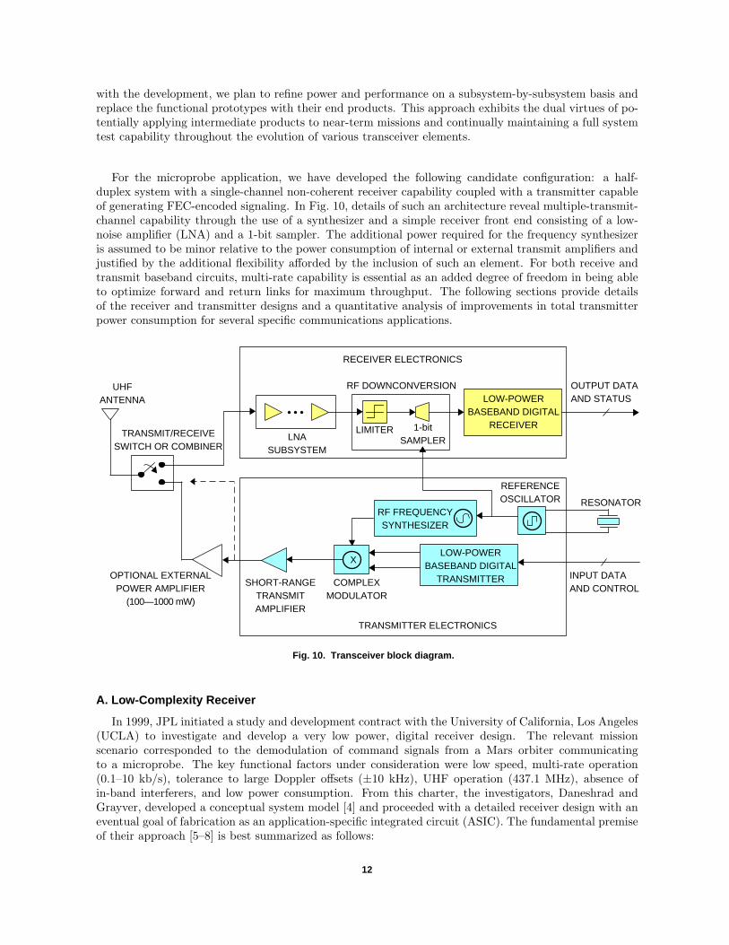
For the microprobe application, we have developed the following candidate configuration: a half-duplex system with a single-channel non-coherent receiver capability coupled with a transmitter capableof generating FEC-encoded signaling. In Fig. 10, details of such an architecture reveal multiple-transmit-channel capability through the use of a synthesizer and a simple receiver front end consisting of a low-noise amplifier (LNA) and a 1-bit sampler. The additional power required for the frequency synthesizeris assumed to be minor relative to the power consumption of internal or external transmit amplifiers andjustified by the additional flexibility afforded by the inclusion of such an element. For both receive andtransmit baseband circuits, multi-rate capability is essential as an added degree of freedom in being ableto optimize forward and return links for maximum throughput. The following sections provide detailsof the receiver and transmitter designs and a quantitative analysis of improvements in total transmitterpower consumption for several specific communications applications.
LOW-POWERBASEBAND DIGITAL
RECEIVER
RECEIVER ELECTRONICS
RF DOWNCONVERSION
LIMITER 1-bitSAMPLERLNA
SUBSYSTEM
UHFANTENNA
TRANSMITTER ELECTRONICS
TRANSMIT/RECEIVESWITCH OR COMBINER
OUTPUT DATAAND STATUS
INPUT DATAAND CONTROL
RESONATOR
REFERENCEOSCILLATOR
LOW-POWERBASEBAND DIGITAL
TRANSMITTER
RF FREQUENCYSYNTHESIZER
COMPLEXMODULATOR
SHORT-RANGETRANSMITAMPLIFIER
OPTIONAL EXTERNALPOWER AMPLIFIER
(100—1000 mW)
X
Fig. 10. Transceiver block diagram.
A. Low-Complexity Receiver
In 1999, JPL initiated a study and development contract with the University of California, Los Angeles(UCLA) to investigate and develop a very low power, digital receiver design. The relevant missionscenario corresponded to the demodulation of command signals from a Mars orbiter communicatingto a microprobe. The key functional factors under consideration were low speed, multi-rate operation(0.1–10 kb/s), tolerance to large Doppler offsets (±10 kHz), UHF operation (437.1 MHz), absence ofin-band interferers, and low power consumption. From this charter, the investigators, Daneshrad andGrayver, developed a conceptual system model [4] and proceeded with a detailed receiver design with aneventual goal of fabrication as an application-specific integrated circuit (ASIC). The fundamental premiseof their approach [5–8] is best summarized as follows:
12

(1) Simplify the front-end architecture to allow digital processing as early as possible in thereceiver chain.
(2) Realize as a digital integrated circuit that is easily ported between different fabricationprocesses.
(3) Utilize complementary metal oxide semiconductor (CMOS) digital processing for lowpower consumption (proportional to the clock rate).
(4) Select non-coherent detection to avoid acquisition and tracking complexities with coher-ent systems.
(5) Assume the absence of interferers, allowing 1-bit processing to reduce receiver complexity.
(6) Accept some degradation to achieve the lowest power consumption possible.
Details of the receiver system architecture are shown in Fig. 11. For simplicity, the receiver is designedto operate at a single frequency. The overall system design requires that the front end need performonly low-noise amplification, narrowband bandpass filtering, and subsampling of the carrier signal. Thebandpass filtering is based on surface acoustic wave (SAW) filter technology and, for devices operating inthe UHF range, are capable of achieving an RF bandwidth of roughly 500 kHz. Based on this bandwidth,1.2 MHz is the minimum allowable subsampling rate to avoid noise aliasing and enable quadrature sam-pling of the 437.1-MHz carrier [4,9]. After quadrature sampling and demultiplexing, the 1-bit samplesare downsampled by a 24:1 ratio to further lower the CMOS processing rate for power conservation.Depending on the data rate, the signal will be either directly detected (10 kb/s) using a 16-point discreteFourier transform (DFT) or frequency compensated via direct digital frequency synthesis (DDFS) andfurther downsampled by factors of ten through one (1 kb/s) or two (100 b/s) stages prior to final DFTdetection. Other features incorporated into this design include programmability of the following param-eters: modulation index, packet unique word length and value, and thresholds for frequency and timingacquisition.
This design was fabricated through a MOSIS submission using the Taiwan Semiconductor Manufac-turing Company’s 0.25-µm CMOS process. Preliminary tests indicated basic functional operation for the10 packaged prototypes delivered from the foundry. The combined core and input/output (I/O) powerconsumption required by these baseband FSK receivers ranges from 0.6 to 4.3 mW for operating voltagesof 1.0 and 2.5 V.
In order to evaluate the performance of the baseband receiver ASIC under realistic command signal con-ditions, we have initially implemented the required front-end functionality called for in the low-complexity
X
1 kb/s and 100 b/s
100 b/s
ALL-DIGITAL CIRCUITRY
50 kHz
1.2-MHzSAMPLE
RATE
1-bitADC X 24:1
1,i,−1,−i
DDFS1
DDFS2
10:1 5 kHz
0.5 kHz
16-pointDFT
DE
CIS
ION
437.1-MHzCARRIER
FREQUENCY
SAWBPF
X 10:1
Fig. 11. Low-power receiver functionality.
13
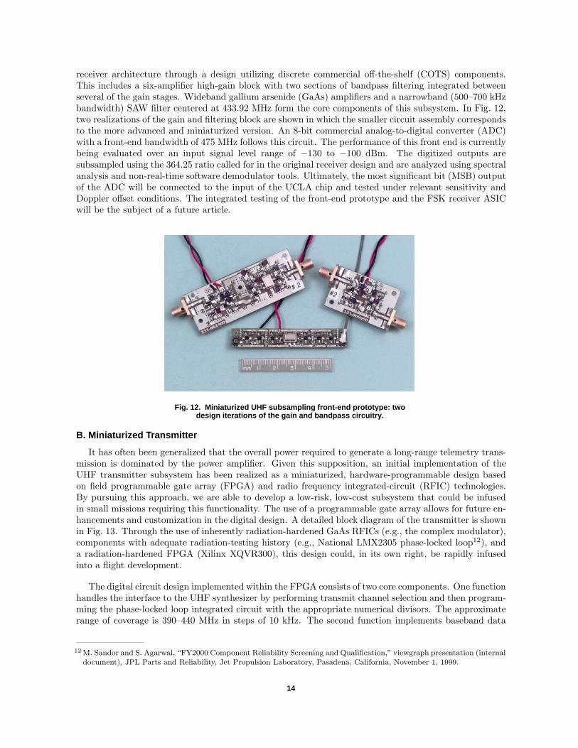
receiver architecture through a design utilizing discrete commercial off-the-shelf (COTS) components.This includes a six-amplifier high-gain block with two sections of bandpass filtering integrated betweenseveral of the gain stages. Wideband gallium arsenide (GaAs) amplifiers and a narrowband (500–700 kHzbandwidth) SAW filter centered at 433.92 MHz form the core components of this subsystem. In Fig. 12,two realizations of the gain and filtering block are shown in which the smaller circuit assembly correspondsto the more advanced and miniaturized version. An 8-bit commercial analog-to-digital converter (ADC)with a front-end bandwidth of 475 MHz follows this circuit. The performance of this front end is currentlybeing evaluated over an input signal level range of −130 to −100 dBm. The digitized outputs aresubsampled using the 364.25 ratio called for in the original receiver design and are analyzed using spectralanalysis and non-real-time software demodulator tools. Ultimately, the most significant bit (MSB) outputof the ADC will be connected to the input of the UCLA chip and tested under relevant sensitivity andDoppler offset conditions. The integrated testing of the front-end prototype and the FSK receiver ASICwill be the subject of a future article.
Fig. 12. Miniaturized UHF subsampling front-end prototype: twodesign iterations of the gain and bandpass circuitry.
B. Miniaturized Transmitter
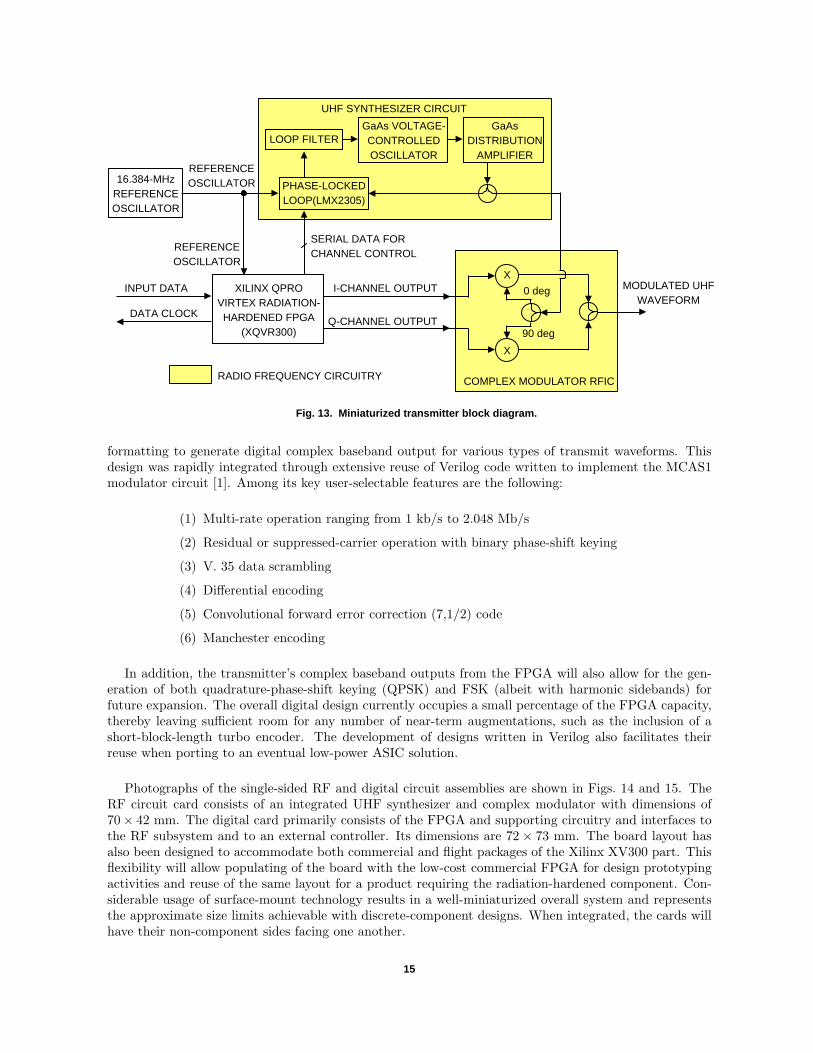
It has often been generalized that the overall power required to generate a long-range telemetry trans-mission is dominated by the power amplifier. Given this supposition, an initial implementation of theUHF transmitter subsystem has been realized as a miniaturized, hardware-programmable design basedon field programmable gate array (FPGA) and radio frequency integrated-circuit (RFIC) technologies.By pursuing this approach, we are able to develop a low-risk, low-cost subsystem that could be infusedin small missions requiring this functionality. The use of a programmable gate array allows for future en-hancements and customization in the digital design. A detailed block diagram of the transmitter is shownin Fig. 13. Through the use of inherently radiation-hardened GaAs RFICs (e.g., the complex modulator),components with adequate radiation-testing history (e.g., National LMX2305 phase-locked loop12), anda radiation-hardened FPGA (Xilinx XQVR300), this design could, in its own right, be rapidly infusedinto a flight development.
The digital circuit design implemented within the FPGA consists of two core components. One functionhandles the interface to the UHF synthesizer by performing transmit channel selection and then program-ming the phase-locked loop integrated circuit with the appropriate numerical divisors. The approximaterange of coverage is 390–440 MHz in steps of 10 kHz. The second function implements baseband data
12 M. Sandor and S. Agarwal, “FY2000 Component Reliability Screening and Qualification,” viewgraph presentation (internaldocument), JPL Parts and Reliability, Jet Propulsion Laboratory, Pasadena, California, November 1, 1999.
14
RADIO FREQUENCY CIRCUITRY
MODULATED UHFWAVEFORM
INPUT DATA
DATA CLOCK
I-CHANNEL OUTPUT
Q-CHANNEL OUTPUT
XILINX QPROVIRTEX RADIATION-HARDENED FPGA
(XQVR300)
16.384-MHzREFERENCEOSCILLATOR
UHF SYNTHESIZER CIRCUIT
LOOP FILTER
PHASE-LOCKEDLOOP(LMX2305)
SERIAL DATA FORCHANNEL CONTROL
GaAsDISTRIBUTION
AMPLIFIER
X
X
COMPLEX MODULATOR RFIC
90 deg
0 deg
REFERENCEOSCILLATOR
REFERENCEOSCILLATOR
Fig. 13. Miniaturized transmitter block diagram.
GaAs VOLTAGE-CONTROLLEDOSCILLATOR
formatting to generate digital complex baseband output for various types of transmit waveforms. Thisdesign was rapidly integrated through extensive reuse of Verilog code written to implement the MCAS1modulator circuit [1]. Among its key user-selectable features are the following:
(1) Multi-rate operation ranging from 1 kb/s to 2.048 Mb/s
(2) Residual or suppressed-carrier operation with binary phase-shift keying
(3) V. 35 data scrambling
(4) Differential encoding
(5) Convolutional forward error correction (7,1/2) code
(6) Manchester encoding
In addition, the transmitter’s complex baseband outputs from the FPGA will also allow for the gen-eration of both quadrature-phase-shift keying (QPSK) and FSK (albeit with harmonic sidebands) forfuture expansion. The overall digital design currently occupies a small percentage of the FPGA capacity,thereby leaving sufficient room for any number of near-term augmentations, such as the inclusion of ashort-block-length turbo encoder. The development of designs written in Verilog also facilitates theirreuse when porting to an eventual low-power ASIC solution.
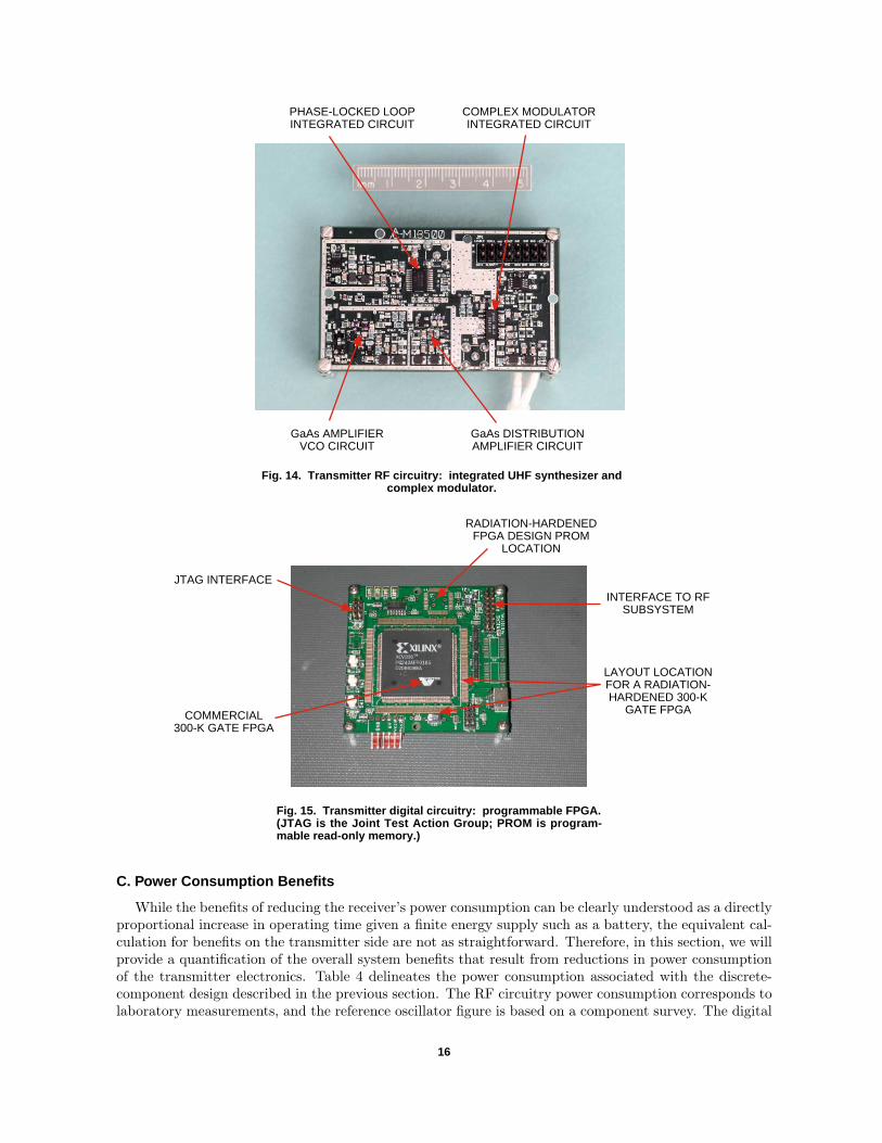
Photographs of the single-sided RF and digital circuit assemblies are shown in Figs. 14 and 15. TheRF circuit card consists of an integrated UHF synthesizer and complex modulator with dimensions of70× 42 mm. The digital card primarily consists of the FPGA and supporting circuitry and interfaces tothe RF subsystem and to an external controller. Its dimensions are 72× 73 mm. The board layout hasalso been designed to accommodate both commercial and flight packages of the Xilinx XV300 part. Thisflexibility will allow populating of the board with the low-cost commercial FPGA for design prototypingactivities and reuse of the same layout for a product requiring the radiation-hardened component. Con-siderable usage of surface-mount technology results in a well-miniaturized overall system and representsthe approximate size limits achievable with discrete-component designs. When integrated, the cards willhave their non-component sides facing one another.
15
PHASE-LOCKED LOOPINTEGRATED CIRCUIT
COMPLEX MODULATORINTEGRATED CIRCUIT
GaAs AMPLIFIERVCO CIRCUIT
GaAs DISTRIBUTIONAMPLIFIER CIRCUIT
Fig. 14. Transmitter RF circuitry: integrated UHF synthesizer andcomplex modulator.
RADIATION-HARDENEDFPGA DESIGN PROM
LOCATION
INTERFACE TO RFSUBSYSTEM
LAYOUT LOCATIONFOR A RADIATION-HARDENED 300-K
GATE FPGACOMMERCIAL300-K GATE FPGA
JTAG INTERFACE
Fig. 15. Transmitter digital circuitry: programmable FPGA.(JTAG is the Joint Test Action Group; PROM is program-mable read-only memory.)
C. Power Consumption Benefits
While the benefits of reducing the receiver’s power consumption can be clearly understood as a directlyproportional increase in operating time given a finite energy supply such as a battery, the equivalent cal-culation for benefits on the transmitter side are not as straightforward. Therefore, in this section, we willprovide a quantification of the overall system benefits that result from reductions in power consumptionof the transmitter electronics. Table 4 delineates the power consumption associated with the discrete-component design described in the previous section. The RF circuitry power consumption corresponds tolaboratory measurements, and the reference oscillator figure is based on a component survey. The digital
16

Table 4. Discrete RF transmitter circuit powerrequirements (power amplifier excluded).
EstimatedTransmitter circuit element power
consumption, mW
Integrated synthesizer and 335a
complex modulator
Reference oscillator 15b
Digital modulator ASIC 20c
Total power consumption 370
a Measured power consumption of miniaturizedtransmitter RF circuitry.
b From a survey of various commercial temperature-compensated crystal oscillator (TCXO) manufac-turers.
c Estimate based on approximate gate count ofFPGA modulator design.
modulator ASIC consumption corresponds to an extrapolation of the FPGA design implemented as alow-power CMOS integrated circuit. The 370-mW power figure represents the required expenditure toperform bit encoding and formatting, synthesized UHF local oscillator generation, and direct upconversionof digital complex baseband signals, resulting in a modulated signal level of several milliwatts. In thefollowing examples, we compare the discrete design power consumption to our 50-mW goal.
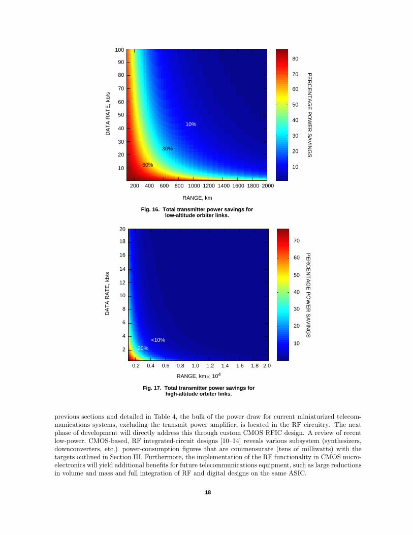
In Figs. 16 and 17, we assess the percentage power savings achieved for surface-to-orbit return-linksituations. The parameter space and RF transmit power levels, respectively, correspond to a Mars polarorbiter, Fig. 2, and an areostationary orbiter, Fig. 3. The color map on the right-hand side of the figuresprovides the legend that relates specific colors to the percentage improvement. We arrive at the resultsshown in these figures by comparing the total power consumption of the discrete-component design ofthe modulator electronics versus a complete mixed-signal integrated-circuit solution. Factored into theoverall consumption is the power requirement of an RF power amplifier that achieves an efficiency of35 percent. Clearly, some significant savings can be achieved for the low-altitude orbiter application.Power savings of 30 to 60 percent are achieved over a return-link data-rate range of 10 to 70 kb/s forslant paths of 400 to 900 km. The benefit drops off quickly as both range and rate are increased. Thiseffect is strongly reinforced in Fig. 16, which indicates that negligible benefits ensue for a high-altitudeorbiter application.
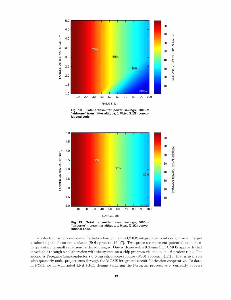
A similar analysis is performed for the high-rate, 1-Mb/s, “air”-to-ground links previously examined inFigs. 8 and 9. We again determine the benefit of reduced power consumption for a low-power integrated-circuit realization of the modulator’s digital and RF electronics. For both 2- and 5-km transmitteraltitudes, shown in Figs. 18 and 19, a greater than 50 percent improvement is achieved out to a rangeof 50 km, and better than 30 percent is obtained out to 100 km, provided that the received antennaheights are maintained above 3 and 1 m, respectively. When the slant range is restricted to 30 km or less,free-space path loss is applicable to both scenarios for all antenna heights, resulting in a very significantbenefit of greater than 70 percent power savings.
D. Future Development
Thus far, we have shown the beneficial impact of reducing power consumption for both the receiverand transmitter electronics for several specific Mars in situ communications examples. As discussed in
17
400 800 2000
RANGE, km
30
50
60
70
80
90
100
30%
DA
TA
RA
TE
, kb/
sP
ER
CE
NT
AG
E P
OW
ER
SA
VIN
GS
50
30
20
10
Fig. 16. Total transmitter power savings forlow-altitude orbiter links.
10%
1200 1600 1800
40
80
14001000600200
60%
20
10
70
60
40
0.2 0.4 0.6 0.8 1.0 1.2 1.4 1.6 1.8 2.0
RANGE, km 104
2
4
6
8
10
12
14
16
18
20
20%
DA
TA
RA
TE
, kb/
sP
ER
CE
NT
AG
E P
OW
ER
SA
VIN
GS
70
60
50
40
30
20
10
Fig. 17. Total transmitter power savings forhigh-altitude orbiter links.
<10%
previous sections and detailed in Table 4, the bulk of the power draw for current miniaturized telecom-munications systems, excluding the transmit power amplifier, is located in the RF circuitry. The nextphase of development will directly address this through custom CMOS RFIC design. A review of recentlow-power, CMOS-based, RF integrated-circuit designs [10–14] reveals various subsystem (synthesizers,downconverters, etc.) power-consumption figures that are commensurate (tens of milliwatts) with thetargets outlined in Section III. Furthermore, the implementation of the RF functionality in CMOS micro-electronics will yield additional benefits for future telecommunications equipment, such as large reductionsin volume and mass and full integration of RF and digital designs on the same ASIC.
18
20 40 100
RANGE, km
1.0
1.5
2.5
3.0
3.5
4.0
4.5
5.0
50%LA
ND
ER
AN
TE
NN
A H
EIG
HT
, mP
ER
CE
NT
AG
E P
OW
ER
SA
VIN
GS
50
40
30
20
10
Fig. 18. Total transmitter power savings, 2000-m"airborne" transmitter altitude, 1 Mb/s, (7,1/2) convo-lutional code.
30%
<10%
60 80 90
2.0
60
70503010
70%
70
80
20 40 100
RANGE, km
1.0
1.5
2.5
3.0
3.5
4.0
4.5
5.0
LAN
DE
R A
NT
EN
NA
HE
IGH
T, m
PE
RC
EN
TA
GE
PO
WE
R S
AV
ING
S
50
40
30
20
10
Fig. 19. Total transmitter power savings, 5000-m"airborne" transmitter altitude, 1 Mb/s, (7,1/2) convo-lutional code.
60 80 90
2.0
60
70503010
70
80
50%
30%
70%
In order to provide some level of radiation hardening in a CMOS integrated-circuit design, we will targeta mixed-signal silicon-on-insulator (SOI) process [15–17]. Two processes represent potential candidatesfor prototyping small radiation-hardened designs. One is Honeywell’s 0.35-µm SOI CMOS approach thatis available through a collaboration with the system-on-a-chip program via annual multi-project runs. Thesecond is Peregrine Semiconductor’s 0.5-µm silicon-on-sapphire (SOS) approach [17,18] that is availablewith quarterly multi-project runs through the MOSIS integrated-circuit fabrication cooperative. To date,in FY01, we have initiated LNA RFIC designs targeting the Peregrine process, as it currently appears
19

to offer greater fabrication opportunities for multiple design iterations during each year. It is anticipatedthat the high levels of RF and digital integration on radiation-hardened SOI CMOS will ultimately enablenew generations of deep-space missions with highly constrained mass and power resources. Furthermore,through modular subsystem development, significant reuse and tailored communications systems solutionsshould result from these technology investments
IV. Summary
We have described transceiver technology development activities oriented towards very low powertelecommunication systems to be used for in situ communications applications. In addition, severalquantitative examples of Mars communications scenarios were developed to identify the approximaterange and data-rate capabilities associated with this class of telecommunications equipment. Theseinclude UHF links between a surface element and an orbiter, and short-range ground-to-ground andlonger-range “air”-to-ground configurations.
The use of uncoded modulations and non-coherent detection on the forward polar orbiter-to-landerlink was shown to be a viable choice that could simplify the implementation of low-to-medium data rate,low-power consumption command receivers for resource-constrained missions such as a microprobe. Theevaluation of surface links further showed that, over relatively flat terrain, low data rates and a range ofless than 2 km can be supported with transmitter powers of less than 1 W. In the “airborne” scenario, longdistance (approaching 100 km), high-rate, FEC-encoded links of 1 Mb/s can be achieved with severalhundred milliwatts of transmit power provided the transmitting “airborne” platform is located at analtitude of several kilometers.
A transceiver architecture targeting the communications link between a surface microprobe and relayorbiter has been developed, and constituent elements of the receiver and transmitter are in variousstages of prototyping and functional testing. The current receiver prototype consists of a high-gain,subsampling front end, followed by an ultra-low-power, multi-rate, FSK receiver ASIC fabricated in CMOStechnology. The gain and sampling portions of the front end have been realized as a miniaturized, medium-power-consumption, discrete-component design for the purposes of testing the ASIC performance. Initialtests performed on the ASIC confirm its ultra-low-power operation (0.2 to 1.5 mW depending uponsupply voltage), and more detailed bit-error-rate tests under relevant channel conditions are planned forcompletion in the near future. The current transmitter prototype has been developed as a hardwareprogrammable, miniaturized, discrete-component design. The design employs numerous componentsapplicable to a flight regime (e.g., radiation-tolerant or -hardened devices) to enable rapid infusion, inwhole or in part, into the development cycle for a suitable mission. To attain very low power consumptionfor both the transmitter and receiver, the next development phase calls for microelectronic integration ofthe RF circuitry. Initial receiver front-end design efforts have targeted Peregrine Semiconductor’s silicon-on-sapphire (SOS) CMOS as a suitable process for eventual integration of the entire transceiver’s RF anddigital circuitry, ultimately leading to a radio-on-a-chip implementation suitable for a variety of in situcommunication needs.
Acknowledgments
The work described in this article represents the composite compilation ofinsights and work performed by numerous individuals on a variety of projects.Both detailed and/or informal discussions with each of the following have con-tributed valuable ideas towards the use and development of highly miniaturized,
20
low-power transceivers for deep-space applications. These individuals include BabakDaneshrad, Gary Stevens, Martin Agan, Eric Archer, David Bell, Polly Estabrook,Eugene Grayver, Edwin Grigorian, David Hansen, John Huang, Thomas Jedrey,Douglas Price, and Sarita Thakoor.
References
[1] M. Agan, A. Gray, E. Grigorian, D. Hansen, E. Satorius, and C. Wang, “MicroCommunications and Avionics Systems First Prototype (MCAS1): A Low Power,Low Mass In Situ Transceiver,” The Telecommunications and Mission OperationsProgress Report 42-138, April–June 1999, Jet Propulsion Laboratory, Pasadena,California, pp. 1–35, August 15, 1999.http://tmo.jpl.nasa.gov/tmo/progress report/42-138/138I.pdf
[2] W. Lindsey and M. Simon, Telecommunication Systems Engineering, EnglewoodCliffs, New Jersey: Prentice Hall, 1973.
[3] J. Odenwalder, Error Control Coding Handbook, Final Report, Linkabit Corpo-ration Contract No. F44620-76-C-0056 to U.S. Air Force, distributed by DefenseTechnical Information Center, July 15, 1976.
[4] E. Grayver and B. Daneshrad, “A Low Power FSK Receiver for Space Applica-tions,” IEEE Wireless Communications and Networking Conference, 2000, vol. 2,pp. 713–718, 2000.
[5] E. Grayver and B. Daneshrad, “A Self-Contained 100 µW Multirate FSK Re-ceiver ASIC,” IEEE International Solid-State Circuits Conference, p. 332, 2001.
[6] E. Grayver and B. Daneshrad, “A Low-Power All-Digital FSK Receiver for SpaceApplications,” IEEE Transactions on Communications, vol. 49, no. 5, pp. 911–921, May 2001.
[7] E. Grayver and B. Daneshrad, “Direct Digital Frequency Synthesis Using a Mod-ified CORDIC,” IEEE International Symposium on Circuits and Systems, vol. 5,pp. 241–244, 1998.
[8] E. Grayver, An Ultra-low-power FSK Receiver for Space and Terrestrial Com-munications, Ph.D. Dissertation, University of California, Los Angeles, 2000.
[9] R. Vaughan, N. Scott, and D. White, “The Theory of Bandpass Sampling,” IEEETransactions on Signal Processing, vol. 39, no. 9, pp. 1973–1984, September 1991.
[10] P. Baltus and R. Dekker, “Optimizing RF Front Ends for Low Power,” Proceed-ings of the IEEE, vol. 88, no. 10, pp. 1546–1559, October 2000.
[11] T. Lee and S. Wong, “CMOS RF Integrated Circuits at 5 GHz and Beyond,”Proceedings of the IEEE, vol. 88, no. 10, pp. 1560–1571, October 2000.
[12] H. Rategh, H. Samavati, and T. Lee, “A CMOS Frequency Synthesizer with anInjection-Locked Frequency Divider for a 5-GHz Wireless LAN Receiver,” IEEEJournal on Solid-State Circuits, vol. 35, no. 5, pp. 780–787, May 2000.
21
[13] J.-K. Goo, K.-H. Oh, C.-H. Choi, Z. Yu, T. H. Lee, and R. W. Dutton, “Guide-lines for the Power Constrained Design of a CMOS Tuned LNA,” Simulation ofSemiconductor Processes and Devices, 2000, SISPAD 2000 International Confer-ence, Seattle, Washington, pp. 269–272, September 6008, 2000.
[14] R. Reedy, J. Cable, and D. Kelly, “Single Chip Wireless Systems Using SOI,”1999 IEEE International SOI Conference, Rohnert Park, California, pp. 8–11,October 1999.
[15] M. Stuber, P. Dennies, G. Lyons, T. Kobayashi, and H. Domyo, “A Manufac-turable SOI CMOS Process for Low Power Digital, Analog, and RF Applica-tions,” 1997 IEEE International SOI Conference, Fish Camp, California, pp. 70–71, October 1997.
[16] M. Stuber, M. Megahed, J. Lee, T. Kobayashi, and H. Domyo, “SOI CMOS withHigh-Performance Passive Components for Analog, RF, and Mixed Signal De-sign,” 1998 IEEE International SOI Conference, Stuart, Florida, p. 99, October1998.
[17] M. Megahed, M. Burgener, J. Cable, R. Benton, D. Staab, M. Stuber, P. Dennies,and R. Reedy, “Low Cost UTSI Technology for RF Wireless Applications,” 1998IEEE MTT-S Digest, pp. 981–984, 1998.
[18] G. Lyons, “Commercial SOS Technology for Radiation-Tolerant Space Applica-tions,” IEEE Radiation Effects Data Workshop 1998, Newport Beach, California,pp. 96–99, July 1998.
22