Embed Size (px)
Citation preview

Coupling Phenomena and Applications, by S.Donati, Univ Pavia
Developing 3Developing 3--D Imaging D Imaging SensorsSensors
Problems and TechnologiesProblems and Technologies
SilvanoSilvano DonatiDonatiDepartment of Electronics, University of Pavia, Italy
web: http://www-3.unipv.it/donati

OutlineOutline
• outlook to 3D applications
• time‐of‐flight measuring technique
• comparing PULSED and SWM approaches
• developing the Photo‐demodulator in CMOS
• measurements and conclusions

33--D ImagingD Imaging
adding distance information
Today’s technology is ready to develop photodetectorsfor the three‐dimensional world !!
2D2D
pixels describethe intensitypattern I(x,y)
pixels describe morphologyz(x,y)

typical applicationstypical applications
• Homeland security
• Navigation aids
• Virtual reality
• Robotics
• Cultural heritage
• Ambient assisted living

techniques for 3D imagingtechniques for 3D imaging
• Triangulation
• Interferometry
• Time-of-flight(pulsed or SWM)
Compact, may be scannerlessFast acquisitionLarge distance rangeCost-effective
Active (illuminator required)Ambiguity range limitation
bulky, requires scanningshort distancemedium/low resolution
very high resolutionexpensive, critical to operate

TimeTime--ofof--Flight rangefindersFlight rangefinders
SW (sine wave)Modulated
Dt
Time
Opt
ical
Pow
er
ΔτD =
c Δτ2
Emitted
Received
PULSED
Δτ

both both PULSEDPULSED and and SWSW 33--DD developments developments should entail: should entail: -- integration of timeintegration of time--ofof--flight pixelflight pixelonon--board technology with the Siliconboard technology with the SiliconCMOS industry standard (and CMOS industry standard (and ……lowlow--cost cost !!) technology!!) technology
-- minimum invasiveness (optical power)minimum invasiveness (optical power)of the active illumination required of the active illumination required
in most applications, to be interestingin most applications, to be interesting……

analyzing Timeanalyzing Time--ofof--Flight rangefinders:Flight rangefinders:pulsed pulsed vsvs SWMSWM
1 mW
1 nW
1 μW
1 pW
10 k1k10010
re
ceive
r
noise
pow
er
nP =
r
λ=0.85 μm S/N = 10 D =100mm
normalized distance L/¦T (m)atm
1m
1
1k
1M
equivalent power G P (W)
s
1.0
SW m
odula
ted
topo
grap
h
puls
ed
telem
eter
3-D ca
mer
a
theoretically equivalentat the quantum limit at equal average power,but PULSED is lesssensitive to stray light,has some safety issuesand requires more bandwidth to circuits.SW-modulated is short-distance, is abouteyesafe, but has rangeambiguity to circumvent
GPs = (S/N) Pn 4Leq2/Dr
2

other features of PULSEDother features of PULSED and and SWSW
-- Pulsed 3Pulsed 3--D requires a fast (subD requires a fast (sub--ns) detector ns) detector for operation on short distances, and very fast for operation on short distances, and very fast time sorters to measure the nstime sorters to measure the ns--range time range time delay delay SPADsSPADs and Counters with TACand Counters with TAC--this makes the pixel large and fillthis makes the pixel large and fill--factor low, factor low, requiring a lensrequiring a lens--array for sensitivity recoveryarray for sensitivity recovery-- SW works on moderate frequency (20 to 100 SW works on moderate frequency (20 to 100 MHz) for 3MHz) for 3--D short range, and by incorporating D short range, and by incorporating a demodulator into the detector circuits are a demodulator into the detector circuits are greatly simplified, and fillgreatly simplified, and fill--factor is highfactor is high

detour on the detour on the PULSEDPULSED 33--DD approachapproach-- in 3in 3--D, D, PULSEDPULSED is a competitor to SWM is a competitor to SWM but calls for a fast (subbut calls for a fast (sub--ns) detector able to ns) detector able to resolve the subresolve the sub--ns propagation times of ns propagation times of shortshort--range applicationsrange applications
-- the the SPADSPAD (Single Photon Avalanche Detector)(Single Photon Avalanche Detector)is the suitable choice of is the suitable choice of photosensorphotosensor
-- SPADSPAD is compatible to fine is compatible to fine CMOS CMOS technologytechnology-- anan FETFET--STREP STREP European ProgramEuropean Program pursuedpursued
development of a 120development of a 120--nm CMOS 3nm CMOS 3--D and fastD and fastspectroscopy imaging (spectroscopy imaging (32x3232x32 and and 128x160128x160pixels) device pixels) device –– the the MEGAFRAMEMEGAFRAME projectproject

a 50 a 50 μμm active diameter devices has been designed m active diameter devices has been designed in 120in 120‐‐nm CMOS with good performances of:nm CMOS with good performances of:
CMOS SPAD parametersCMOS SPAD parameters
high probability of detectionhigh probability of detection(35%@1(35%@1--V overdrive)V overdrive)
low dark counts ratelow dark counts rate(40 Hz for a 6(40 Hz for a 6--μμm m diadia.).)
40
temp (°C)
excess voltage (mV)
0
40
200.2
0.6
ΔV=1.0

and, not less important:and, not less important:
CMOS SPAD parameters IICMOS SPAD parameters II
subsub--ns time resolutionns time resolution(61 (61 psps rmsrms))
low low afterpulsingafterpulsing(negligible @ (negligible @ TThoho>200ns)>200ns)
50 ns

OnOn--board pixel processingboard pixel processingprocessing circuits processing circuits implemented by implemented by CMOS technology CMOS technology in a 50in a 50--μμm m diadia. pixel . pixel area around the area around the 66--μμm SPAD:m SPAD:--active quenchingactive quenching-- premaplifierpremaplifier-- TACTAC--comparatorcomparator--88--bit memorybit memory
Stoppa et al.: ESSCIRC 2009

the CMOS SPAD pixelthe CMOS SPAD pixel……the pixel, 50-μm
by side
……andand the 32x32 the 32x32 arrayarraychip, 4chip, 4--mm mm byby sideside
Stoppa et al.: ESSCIRC 2009
FF FF = = AAph/(A/(Aqc+A+Aph))(~ 0.02 in example above)(~ 0.02 in example above)

fillfill--factor recovery in factor recovery in SPADSPAD
SPAD quenching
and/or sortingcircuits
50 μm
AAphph
AAqcqc
FF FF = = AAphph/(A/(Aqcqc+A+Aphph))~ 0.02 in example above~ 0.02 in example above
then we use a 50then we use a 50--μμm m diadia. . lenslens--array to concentrate array to concentrate
incoming optical powerincoming optical power
0.05
0.1
0.15
0.2
0.25
0
0 5-10 10-5
NA
Z (μm)
C= 35
2520
1510
5
5
10
15
20
30
8-μm
achieved lens array concentration

Example of 3D image pickup with the Example of 3D image pickup with the 32x32 SPAD array32x32 SPAD array
Accuracy:• 1mm (100 frames)
Frame rate:• 1Hz
8-bit digital output

-- thethe SWM is attractive for 3SWM is attractive for 3--D if we canD if we cansimplify data analogue processingsimplify data analogue processing
-- then, we are asked to devise a highthen, we are asked to devise a high--efficiency efficiency photodetectorphotodetector, working with , working with shallow shallow epiepi--layer of a CMOS, low cost,layer of a CMOS, low cost,standard industry process.standard industry process.
-- the answer has been a specially the answer has been a specially designed, CMOSdesigned, CMOS--compatible, high FF, compatible, high FF, photodetectorphotodetector demodulatordemodulator
going back to SWgoing back to SW--modulatedmodulated……

principle of principle of SWMSWM telemetertelemeter
Received Light Echo
DemodulationLO Signal
LP Filter
R(t) = K sin[ωmt ‐Δφ]
M(t) = sin(ωmt + θ) Iph(θ) = K/2 cos(θ+Δφ)
⎟⎟⎠
⎞⎜⎜⎝
⎛−−
=Δ13
24arctanIIII
ϕ
Measured correlation function
recovery of phase Δφ amenable to CMOS integration of the pixel: the detected demodulation signal Iph(t) is sampled on 4-phases θ periods of the local oscillator M(t) so as to supply I1= Iph(θ=0°), I2= Iph(θ=90°), I3= Iph(θ=180°), I4 =Iph(θ=270°), then we compute

let’s now have a look atsensor architecture
o design of a new photo-demodulator
o pixel design
o array architecture

PDD, the PhotoPDD, the Photo--Demodulator DetectorDemodulator Detector
first reported by: Van Nieuwenhove, et al., Proc. Symp. LEOS Benelux Chapter, 229-32 (2005)
M1, M2: modulation electrodes
D1, D2: collection electrodes

more on the PDDmore on the PDD
by pulsing a current IM(50μA typ.) between electrodes M1 and M2, we can switch photocurrent Iph from output D1 to output D2. If current IM is a sine wave, process is a demodulation of the detected signal (wow!)
M1, M2: modulation electrodes, D1, D2: collection electrodes of the photo-demodulator detector (PDD)
pn p n
pn p n
+1 V+3 V +3 V-1 V
+1 V+3 V -1 V +3 V
+-
c
c
M1 M2light
outputIph
outputIph
D1 D2
IM- IM
IM - IM
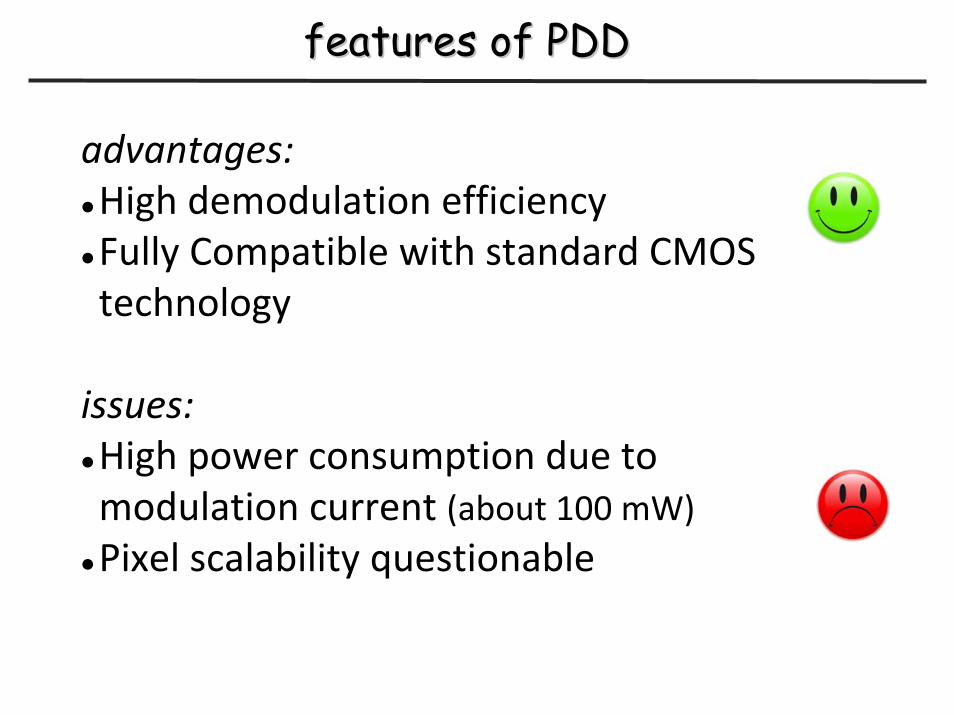
features of PDDfeatures of PDD
advantages:High demodulation efficiencyFully Compatible with standard CMOS technology
issues:High power consumption due to modulation current (about 100 mW)Pixel scalability questionable

Pixel ArchitecturePixel Architecture
• Technology: 180-nm CMOS
• Pixel pitch: 10μm• Fill factor: 24%• 1.8-V transistors

Sensor ArchitectureSensor Architecture
• 120x160 pixel array
• Pseudo-differential pixel
• Column amplifiers
• Output DDS amplifier

Sensor ChipSensor Chip
• CMOS 0.18μm 1P4M process
• Sensor area: 2.5x2.5mm2
•1.8V and 3.3V transistors
• Epitaxial layer
resistivity: 20 Ohm‐cm
thickness: 4μm

• Experimental Results:
o Photo-detector performance
o 3D imaging system

PhotoPhoto--demodulator: DC Performancedemodulator: DC Performance
(ID1‐ID2)(ID1+ID2)
χ=DC demodulationcontrast:
RMOD = 25 kOhmdissipation 10 μW

PhotoPhoto--demodulator: AC Performancedemodulator: AC Performance
(ID1‐ID2)max
(ID1+ID2)χ=
Modulation current:16 μA/pixel (peak)
AC demodulationcontrast:

Noise PerformanceNoise Performance
No appreciable excess noise is observed with respect to the shot‐noise level (IC1≈ 2 nA) due to the modulation resistance
0510152025303540
100 300 500 700 900
Noise Spe
ctral D
ensity
[fA/H
z1/2]
Frequency (Hz)
Total noise (exp.) Amplifier noise (exp.)CAPD noise (exp.) CAPD noise (theor.)

33--D Imaging SystemD Imaging System
Illumination module:• source: LED, 20 MHz, λ: 850nm• power in the FoV: 140 mW• class (IEC 60825-1): 1M
Sensor:• objective 2.9-mm, F/1• sensor FoV 23°x30°• total modulaton current: 400 mA (peak)
Illumination module:• source: LED, 20 MHz, λ: 850nm• power in the FoV: 140 mW• class (IEC 60825-1): 1M
Sensor:• objective 2.9-mm, F/1• sensor FoV 23°x30°• total modulaton current: 400 mA (peak)

Distance MeasurementDistance Measurement
Maximum non‐linearity: 0.3%Distance non uniformity among pixels: 0.2cm

33--D Image ExampleD Image Example
Acquired with 400ms exposure time, 100 lux ambient light

in conclusion...in conclusion...
• Current Assisted Photo-Demodulator-Detector in CMOS technology demonstrated
• 10-μm, 24% fill-factor pixel achieved, • 50% demodulation contrast at 20MHz and • >50MHz cutoff frequency• 120x160 3-D image sensor designed• real-time 3-D Imaging demonstrated, • then……the SWM CMOS 3-D approach is viable !....

謝謝
thank you
Acknowledgement:Acknowledgement:work carried out in work carried out in the the frameframe of a PRIN of a PRIN cooperative cooperative ProgrammeProgramme fundedfunded byby ItalianItalianMURST (MURST (partnerspartners: : UniversitUniversitàà didi PaviaPavia, , Fondazione B. Fondazione B. KesslerKessler, Trento, , Trento, UniversitUniversitààdidi TrentoTrento, , UniversitUniversitàà di Modena e Reggiodi Modena e Reggio))