Embed Size (px)
Citation preview

1
Development of Digital Readout Electronics
for the CMS Tracker
Emlyn Peter Corrin
High Energy Physics Imperial College London
Prince Consort Road London SW7 2BW
Thesis submitted to the University of London for the degree of Doctor of Philosophy
November 2002
2
Abstract The Compact Muon Solenoid (CMS) is a general-purpose detector, based at
CERN in Switzerland, designed to look for new physics in high-energy proton-
proton collisions provided by the Large Hadron Collider. The CMS tracker has 10
million readout channels being sampled at a rate of 40 MHz, then read out at up to
100 kHz, generating huge volumes of data; it is essential that the system can
handle these rates without any of the data being lost or corrupted. The CMS
tracker FED processes the data, removing pedestal and common mode-noise, and
then performing hit and cluster finding. Strips below threshold are discarded,
resulting in a significant reduction in data size. These zero suppressed data are
stored in a buffer before being sent to the DAQ. The processing on the FEDs is
done using FPGAs. Programmable logic was chosen over custom ASICs because
of the lower cost, faster design and verification process, and the ability to easily
upgrade the firmware at a later date.
This thesis is concerned with the digital readout electronics for the CMS
tracker, working on the development of the FED, and verifying that it will meet
the requirements of the detector. Firmware was developed for the back-end FPGA
of the FED, implementing the CMS-wide common data format. Each event is
wrapped in a header/trailer containing information such as the trigger number,
bunch-crossing number and error-detection information. The firmware was
developed in VHDL, and will be incorporated into the back-end FPGA of the
FED, both in the tracker, and in the other subdetectors.
A study was performed, looking into the flow of data and buffer levels in
the FED. A program was written in C++ that models the behaviour of the FED
buffers. It was shown that during normal operation the FED can handle
occupancies of up to 4 % with 100 kHz random triggers, assuming a sustainable
output rate of 200 Mbyte/s. Even when the trigger rate was increased to its
maximum of 140 kHz, the FED buffers did not overflow as long as the occupancy
remained below 2.5 %. These results confirmed that the FED buffers should never
overflow in normal operating conditions.

3
Acknowledgements I would like to thank everyone in the High Energy Physics group for their
help and support during my three years there. In particular Geoff Hall for his
supervision and guidance, Costas Foudas for his help and for spending so much
time proofreading my thesis, and Peter Dornan for letting me work with the
group. Thanks also to John Coughlan, Rob Halsall, Bill Haynes, Peter Sharp, and
Mike Johnson at RAL. I would also like to thank the Particle Physics and
Astronomy Research Council (PPARC) and the Rutherford Appleton Laboratory
(RAL) for funding my project.
I would especially like to thank Greg, Mark, Barry, Jonni, Etam, Rob, and
Matt for the great atmosphere both in the lab and also over a coffee or a pint.
Above all I would like to thank my girlfriend Sandra for her help and moral
support while writing my thesis. Thanks also to my grandmother Win, my sister
Naomi, my mum Marie-Pierre, Laurent, and all the rest of my family.
I dedicate this thesis to my dad, Ian, and my grandfather, George, for
inspiring me towards an inquisitive mind.
4
Contents Abstract....................................................................................................................2
Acknowledgements..................................................................................................3
Contents ...................................................................................................................4
List of Figures..........................................................................................................8
List of Tables .........................................................................................................11
Glossary .................................................................................................................12
Chapter 1: Introduction....................................................................................15
1.1 The Large Hadron Collider (LHC) ........................................................15
1.2 Physics at the LHC ................................................................................16
1.2.1 The Higgs.......................................................................................16
1.2.2 CP Violation ..................................................................................18
1.2.3 Supersymmetry ..............................................................................18
1.3 The Compact Muon Solenoid (CMS)....................................................19
1.3.1 The Magnet ....................................................................................20
1.3.2 The Tracker....................................................................................22
1.3.3 The Electronic Calorimeter (ECAL) .............................................24
1.3.4 The Hadronic Calorimeter (HCAL)...............................................25
1.3.5 The Muon Detectors ......................................................................26
1.3.6 The Trigger ....................................................................................28
1.4 Summary................................................................................................29
Chapter 2: Field Programmable Devices.........................................................30
2.1 Digital Logic..........................................................................................30
2.1.1 Combinatorial Logic......................................................................32
2.1.2 Sequential Logic ............................................................................34
2.2 Programmable Logic .............................................................................34
2.3 History of Programmable Logic ............................................................36
2.3.1 The PROM.....................................................................................36
2.3.2 The PLA and PAL .........................................................................37
2.3.3 The CPLD......................................................................................38
2.3.4 The FPGA......................................................................................39

Contents
5
2.4 Memory Technology .............................................................................40
2.4.1 Fuses and Antifuses .......................................................................40
2.4.2 The EPROM and EEPROM ..........................................................41
2.4.3 SRAM............................................................................................42
2.5 The Xilinx Virtex-II Range of FPGAs ..................................................43
2.5.1 Logic Blocks..................................................................................45
2.5.2 I/O Blocks......................................................................................47
2.5.3 Routing Resources .........................................................................49
2.6 The Design Process................................................................................50
2.6.1 Design Entry ..................................................................................50
2.6.2 Verilog ...........................................................................................52
2.6.3 VHDL ............................................................................................52
2.6.4 Simulation and Synthesis...............................................................54
2.6.5 Device Programming .....................................................................54
2.7 Summary................................................................................................56
Chapter 3: The CMS Tracker Readout System ...............................................57
3.1 Overview................................................................................................57
3.2 The Silicon Detectors ............................................................................58
3.3 The APV Readout Chip .........................................................................59
3.3.1 Preamplifier ...................................................................................61
3.3.2 Shaping Filter.................................................................................61
3.3.3 Pipeline and FIFO..........................................................................61
3.3.4 APSP..............................................................................................61
3.3.5 Analogue Multiplexer....................................................................63
3.3.6 Slow Control..................................................................................64
3.4 The APVMUX.......................................................................................65
3.5 The Optical Link....................................................................................65
3.6 The Front-End Driver ............................................................................66
3.7 The S-LINK64 .......................................................................................67
3.8 The DAQ ...............................................................................................67
3.9 Control and Monitoring .........................................................................68
3.9.1 Timing, Trigger and Control (TTC) ..............................................68
Contents
6
3.9.2 The Tracker Control System (TCS)...............................................69
3.10 Summary................................................................................................69
Chapter 4: The Front-End Driver ....................................................................70
4.1 The FED Front-End Modules ................................................................71
4.2 The Front-End FPGA ............................................................................75
4.2.1 Housekeeping ................................................................................76
4.2.2 Monitoring .....................................................................................77
4.2.3 Configuration.................................................................................77
4.2.4 Data Path........................................................................................78
4.3 The Back-End FPGA.............................................................................82
4.3.1 Common Data Format ...................................................................83
4.3.2 CRC ...............................................................................................84
4.4 Implementation of Common Data Format.............................................86
4.5 Summary................................................................................................92
Chapter 5: Analysis of Data Flow and Buffering in the FED .........................93
5.1 The APV Buffers ...................................................................................94
5.1.1 The APV Emulator ........................................................................94
5.2 Modelling the FED ................................................................................95
5.2.1 Source Data....................................................................................97
5.3 Simulation Results .................................................................................99
5.3.1 Zero-Suppression Mode.................................................................99
5.3.2 Raw-Data Mode...........................................................................108
5.4 Summary..............................................................................................110
Chapter 6: Perspectives .................................................................................111
6.1 FED Schedule ......................................................................................111
6.2 FED Testing.........................................................................................111
6.2.1 JTAG and Boundary Scan Testing ..............................................112
6.2.2 Basic Analogue Tests ..................................................................112
6.2.3 Basic Digital Tests .......................................................................112
6.2.4 More Advanced Tests ..................................................................113
6.3 Conclusions..........................................................................................113
Contents
7
Appendix A: Common Data Format Implementation ...................................115
A.1 fed_data_format.vhd............................................................................115
A.2 builder.vhd ...........................................................................................118
A.3 fifo.vhd.................................................................................................122
A.4 mem64_general.vhd.............................................................................124
A.5 mux.vhd ...............................................................................................125
A.6 pck_crc16_d64_ccitt.vhd.....................................................................126
A.7 pck_crc16_d64_x25.vhd......................................................................128
Appendix B: Common Data Format Verification Code................................132
B.1 testbench.vhd .......................................................................................132
B.2 tester.vhd..............................................................................................135
B.3 main.c...................................................................................................139
B.4 crcmodel.h ...........................................................................................141
B.5 crcmodel.c............................................................................................144
References............................................................................................................147
8
List of Figures Figure 1.1: The LHC site, (a) map, (b) aerial view. ..............................................15
Figure 1.2: Higgs production at the LHC. .............................................................16
Figure 1.3: Principle decay modes of the Higgs at CMS. .....................................17
Figure 1.4: The CMS detector. ..............................................................................19
Figure 1.5: Transverse view of the CMS detector. ................................................20
Figure 1.6: Diagram of the CMS superconducting magnet system.......................21
Figure 1.7: The CMS tracker. ................................................................................22
Figure 1.8: A prototype microstrip detector module from the tracker. .................23
Figure 1.9: An ECAL crystal.................................................................................24
Figure 1.10: An assembled half-barrel of the HCAL. ...........................................25
Figure 1.11: A Muon drift tube..............................................................................26
Figure 1.12: A Muon cathode strip chamber. ........................................................27
Figure 1.13: A Muon resistive plate chamber. ......................................................28
Figure 1.14: The CMS level-1 global trigger. .......................................................29
Figure 2.1: Bipolar transistors (npn and pnp) and their symbols. .........................30
Figure 2.2: JFET transistors (n-channel and p-channel) and their symbols. .........31
Figure 2.3: MOSFET transistors (n-channel and p-channel) and their symbols. ..32
Figure 2.4: A CMOS inverter and transmission gate, and their symbols. .............32
Figure 2.5: CMOS NAND and NOR gates and their symbols. .............................33
Figure 2.6: CMOS transparent latch and flip-flop and their symbols. ..................34
Figure 2.7: Memory used as programmable logic. ................................................36
Figure 2.8: A very small PLA................................................................................37
Figure 2.9: Architecture of a CPLD. .....................................................................38
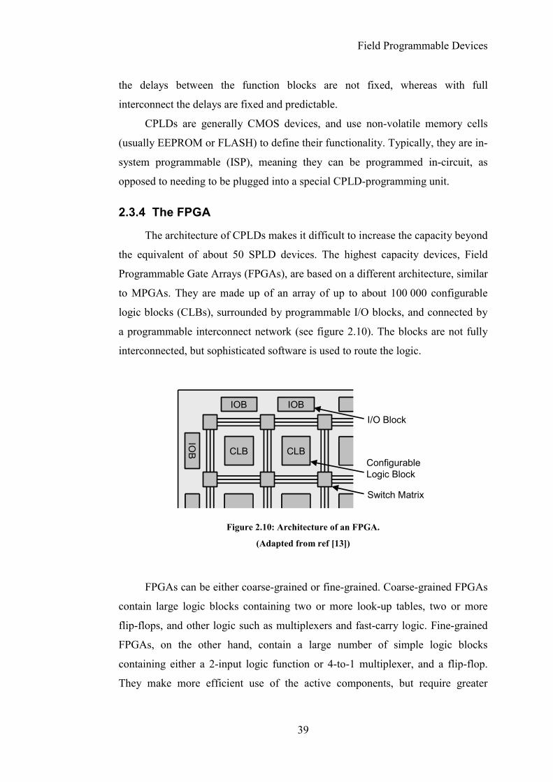
Figure 2.10: Architecture of an FPGA. .................................................................39
Figure 2.11: Example of a fine-grained logic cell. ................................................40
Figure 2.12: Antifuses: (a) ONO, (b) amorphous silicon. .....................................40
Figure 2.13: An EPROM memory cell: a) schematic, b) use in wired-AND........41
Figure 2.14: An SRAM memory cell. ...................................................................42
Figure 2.15: Xilinx Virtex-II Architecture. ...........................................................44
Figure 2.16: Virtex-II logic blocks: (a) CLB, (b) slice..........................................45
List of Figures
9
Figure 2.17: (a) I/O banks in Virtex-II flip-chip packages, (b) an I/O block. .......48
Figure 2.18: Virtex-II routing resources. ...............................................................49
Figure 2.19: The FPGA Design Process................................................................50
Figure 3.1: An overview of the tracker readout system.........................................57
Figure 3.2: A silicon microstrip detector. ..............................................................58
Figure 3.3: The APV25-S1. ...................................................................................60
Figure 3.4: The APV25 APSP circuit....................................................................63
Figure 3.5: A typical APV output frame ...............................................................64
Figure 3.6: The FED and DAQ racks (top) and a FED crate (bottom). ................66
Figure 3.7: Overview of the CMS DAQ system....................................................67
Figure 3.8: Schematic of the tracker control system. ............................................69
Figure 4.1: Schematic of the Front-end driver.......................................................70
Figure 4.2: Schematic of a FED front-end module................................................71
Figure 4.3: Schematic of a FED front-end module analogue section....................72
Figure 4.4: Schematic of a FED front-end module two channel ADC..................73
Figure 4.5: Schematic of the FED front-end FPGA. .............................................75
Figure 4.6: Basic schematic of the housekeeping block........................................76
Figure 4.7: A pair of channels from the datapath block. .......................................78
Figure 4.8: Graphical representation of the clustering algorithm..........................80
Figure 4.9: Diagram of the back-end FPGA..........................................................82
Figure 4.10: Common data format header and trailer............................................83
Figure 4.11: Graphical representation of the CRC algorithm (for CRC-8). ..........85
Figure 4.12: Block diagram of the header formatting block. ................................88
Figure 4.13: A short period of the simulation........................................................90
Figure 5.1: Data flow and buffers in the tracker readout system...........................93
Figure 5.2: The APV Emulator System.................................................................94
Figure 5.3: Graphical representation of the FED buffer model.............................96
Figure 5.4: Distribution of event sizes in strips per detector, from Monte-Carlo. 97
Figure 5.5: Estimated distribution of event sizes in strips per APV......................98
Figure 5.6: Zero-suppression, front-end: events lost vs. output rate. ..................100
Figure 5.7: Zero-suppression, front-end: events lost vs. occupancy. ..................101
Figure 5.8: Zero-suppression, back-end: events lost vs. output rate. ..................102
List of Figures
10
Figure 5.9: Zero-suppression, back-end: events lost vs. occupancy....................103
Figure 5.10: Zero-suppression, back-end: maximum occupancy vs. output rate.104
Figure 5.11: Zero-suppression: peak level of data buffer vs. occupancy. ...........105
Figure 5.12: Zero suppression: peak level of header buffer vs. occupancy. .......106
Figure 5.13: Raw data, front-end: events lost vs. trigger rate..............................108
Figure 5.14: Raw data, back-end: events lost vs. trigger rate..............................109
Figure 5.15: Raw data: maximum trigger rate vs. output rate. ............................110
11
List of Tables Table 2.1: Truth tables for NAND and NOR gates. ..............................................33
Table 2.2: Summary of Programming Technologies.............................................43
Table 2.3: Virtex-II family members.....................................................................45
Table 2.4: Virtex-II block-RAM configurations. ..................................................47
Table 4.1: Rules for data size reduction in the FED..............................................81
Table 4.2: Common data format header and trailer fields. ....................................84
Table 4.3: Parameters for the reference CRC........................................................91
Table 4.4: Synthesis results for the header building code. ....................................91
Table 5.1: Peak header buffer levels....................................................................107
12
Glossary ADC Analogue-to-Digital Converter. APSP Analogue Pulse Shape Processor: Processing stage in the APV
readout chip. APV Analogue Pipeline (Voltage Mode): Front-end readout chip. APV25 APV built on 0.25 µm process. APV6 Early version of the APV built on 1.2 µm process. APVE APV Emulator. APVM Early version of the APV built on 1.2 µm process, for MSGCs. APVMUX APV Multiplexer: Combines the outputs from pairs of APVs to
send to laser driver. ASIC Application Specific Integrated Circuit. BPM BiPhase Mark: Encoding scheme used by the TTC system. BRAM Block-RAM: One of several logic blocks in an FPGA. CCITT Comité Consultatif International de Télégraphique et Téléphonique:
International consultative committee on telecommunications and telegraphy.
CCU Communications and Control Unit: Distributes clock, trigger, control and monitoring data within the tracker.
CERN The European Laboratory for Particle Physics Research, in Geneva, Switzerland.
CLB Configurable Logic Block: Basic unit of logic functionality in FPGAs.
CMOS Complementary Metal Oxide Semiconductor: A semiconductor technology consisting of both p-type and n-type devices, and having low power dissipation.
CMS Compact Muon Solenoid. CPLD Complex Programmable Logic device. CRC Cyclic Redundancy Check: An error detection code. CSC Cathode Strip Chamber: A type of muon detector used at CMS. DAC Digital-to-Analogue Converter. DAQ Data Acquisition system. DCM Digital Clock Manager: One of several logic blocks in an FPGA. DCU Detector Control Unit: Interface to monitor slowly varying
parameters in the tracker. DDR Double Data Rate: Port in which data is latched on both clock
edges, resulting in a doubling of the data rate. DPM Dual Port Memory. DT Drift Tube: A type of muon detector used at CMS. DUT Device Under Test. ECAL Electromagnetic Calorimeter. EEPROM Electrically Erasable Programmable Read Only Memory. EPROM Erasable Programmable Read Only Memory. FEC Front End Controller: Distributes clock, trigger and control data to,
and receives monitoring data from, the tracker readout system via digital optical links.
Glossary
13
FED Front End Driver. FET Field Effect Transistor. FIFO First In First Out: Type of buffer in which the data are read out in
the same order in which they were written. FIR Finite Impulse Response: Type of signal-processing filter. FLASH Type of EEPROM in which large areas of memory can be erased at
once. FPD Field Programmable device: A general term for all types of user-
programmable integrated circuits. FPGA Field Programmable Gate Array: an FPD with a structure allowing
very high logic capacity. HCAL Hadronic Calorimeter. HDL Hardware Description Language. I2C Inter-IC: Two-wire serial communications protocol developed by
Philips. IC Integrated Circuit. IEEE Institute of Electrical and Electronic Engineers: Standards
committee. IIR Infinite Impulse Response: Type of signal-processing filter. ILA Integrated Logic Analyzer: Part of the Chipscope debugging tool
for FPGAs from Xilinx. IOB Input/Output Block. ISP In System Programmable. JFET Junction Field Effect Transistor. JTAG Joint Test Action Group: Standard for controlling and monitoring
pins and internal registers of electronic devices such as FPGAs. L1A Level-1 Accept: First-level trigger decision signal (up to 100 kHz). LEP Large Electron Positron Collider. LHC Large Hadron Collider. LSP Lightest Supersymmetric Particle. LVDS Low Voltage Differential Signalling: High performance, low
power, and low noise signalling standard. MIP Minimum Ionising Particle: Corresponds to roughly 25 000
electrons in a 300 µm thick silicon detector. MOSFET Metal-Oxide-Semiconductor Field Effect Transistor. MPGA Mask Programmable Gate Array: ASIC technology consisting of
standard logic cells (as in an FPGA) but programmed by a custom metal layer during the manufacturing process.
MSGC Microstrip Gas Chamber. MSSM Minimal Supersymmetric Standard Model. NMOS Negative-channel Metal Oxide Semiconductor. OVI Open Verilog International: Non-profit organisation that maintains
Verilog HDL. PAL Programmable Array Logic: Simple FPD with programmable
AND-plane and fixed OR-plane (registered trademark of Advanced Micro Devices Inc.).
PAR Place-and-Route. PCB Printed Circuit Board.
Glossary
14
PCI Peripheral Component Interconnect: Widely used bus designed by Intel.
PLA Programmable Logic Array: Simple FPD with a programmable AND-plane and OR-plane.
PLD Programmable Logic Device: See FPD, often used to refer to relatively simple types of devices.
PMC PCI Mezzanine Card. PMOS Positive-channel Metal Oxide Semiconductor. PPARC Particle Physics and Astronomy Research Council. PROM Programmable Read Only Memory. QDR Quad Data Rate. RAL Rutherford Appleton Laboratory, in Didcot, Oxfordshire. RAM Random Access Memory. ROM Read Only Memory. RPC Resistive Plate Chamber: A type of muon detector used at CMS. SDF Standard Delay Format. S-LINK Protocol for transmission of data in 8-32-bit words at up to 40 MHz S-LINK64 Extension of S-LINK allowing 64-bit data at a rate of 100 MHz. SM Standard Model. SOP Sum of Products. SPLD Simple Programmable Logic Device. SRAM Static RAM. SUSY Supersymmetry. TCS Tracker Control System. TTC Timing, Trigger and Control System. TTCrx TTC Receiver: Custom IC TTL Transistor-Transistor Logic: A semiconductor technology using
bipolar transistors. VHDL VHSIC (Very High Speed Integrated Circuit) Hardware Description
Language. VME Versa Module Europa: A flexible backplane interconnection bus
system, using the Eurocard standard circuit board sizes and defined by IEEE standard 1014-1987.

15
Chapter 1: Introduction
1.1 The Large Hadron Collider (LHC)
The LHC is a particle accelerator being built at CERN, the European
Laboratory for Particle Physics Research near Geneva in Switzerland. It is located
in the 27 km circumference circular tunnel previously used for the Large Electron-
Positron (LEP) collider (see figure 1.1).
When operational, it will provide proton-proton collisions with a centre-of-
mass energy of 14 TeV and a luminosity of 1034 cm-2s-1. This is orders-of-
magnitude higher than any previous accelerator, leading to an extremely
demanding radiation environment. In order to sustain such a high luminosity,
bunches of particles are separated by only 25 ns, and the readout electronics must
be capable of determining from exactly which bunch crossing each signal
originated, leading to very strict timing requirements.
In addition to proton-proton collisions, heavy ions, such as lead, will be
collided at energies in excess of 1000 TeV/ion and luminosity over 1027 cm-2s-1.
Figure 1.1: The LHC site, (a) map, (b) aerial view.
Introduction
16
1.2 Physics at the LHC
The LHC will open up new, previously unexplored, areas of physics. The
energies available will allow many predictions to be either confirmed by
experiment, or rejected. In addition it will allow much more accurate
measurement of many fundamental parameters of physics.
1.2.1 The Higgs
The Standard Model (SM) of particle physics requires the existence of a
new particle, the Higgs. Particles acquire mass through their interaction with the
Higgs field. There is a theoretical upper limit on the mass of the Higgs, of about
1 TeV, and masses up to 114 GeV have been ruled out by direct searches at
LEP [1] and other experiments, although there were hints of a possible Higgs at a
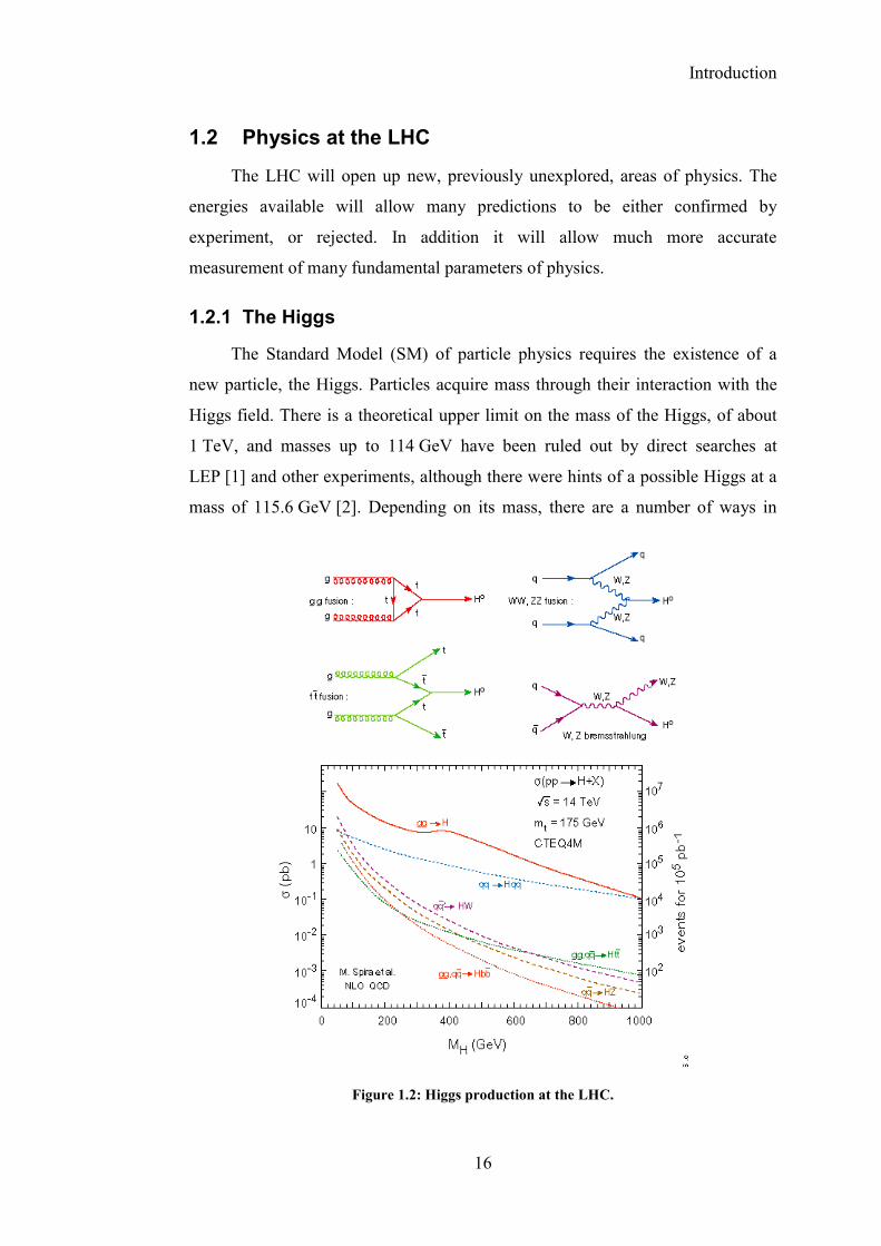
mass of 115.6 GeV [2]. Depending on its mass, there are a number of ways in
Figure 1.2: Higgs production at the LHC.
Introduction
17
which Higgs particles may be produced at the LHC (see figure 1.2), but the
dominant production channel is by gluon fusion. Once produced, there are a
number of different ways the Higgs may decay, also depending on its mass. The
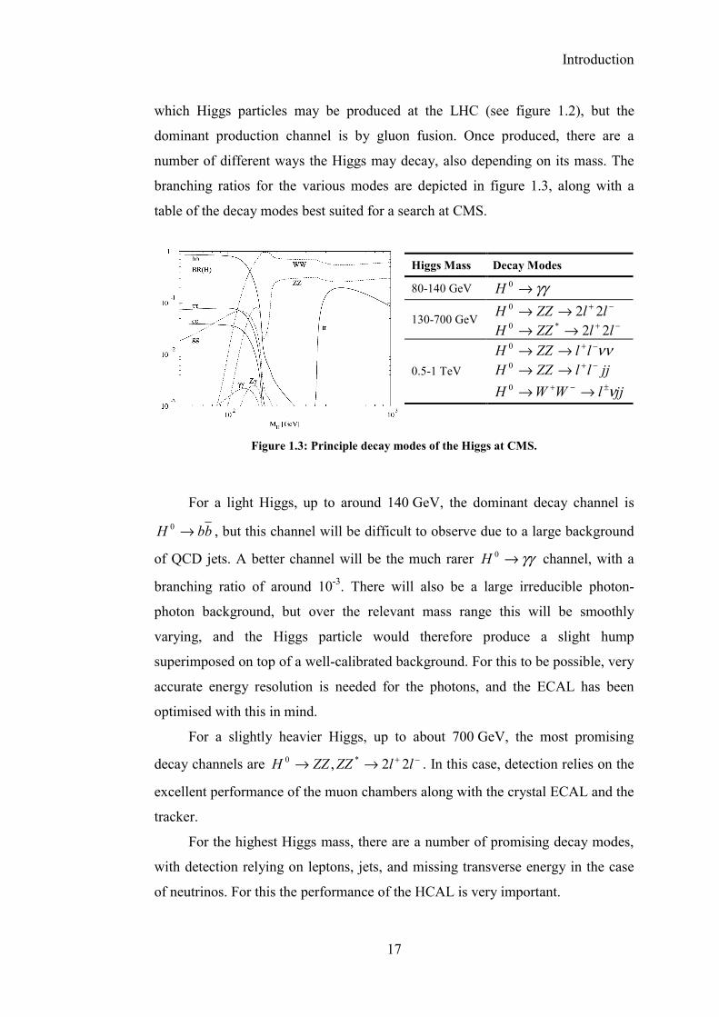
branching ratios for the various modes are depicted in figure 1.3, along with a
table of the decay modes best suited for a search at CMS.
For a light Higgs, up to around 140 GeV, the dominant decay channel is
bbH →0 , but this channel will be difficult to observe due to a large background
of QCD jets. A better channel will be the much rarer γγ→0H channel, with a
branching ratio of around 10-3. There will also be a large irreducible photon-
photon background, but over the relevant mass range this will be smoothly
varying, and the Higgs particle would therefore produce a slight hump
superimposed on top of a well-calibrated background. For this to be possible, very
accurate energy resolution is needed for the photons, and the ECAL has been
optimised with this in mind.
For a slightly heavier Higgs, up to about 700 GeV, the most promising
decay channels are −+→→ llZZZZH 22, *0 . In this case, detection relies on the
excellent performance of the muon chambers along with the crystal ECAL and the
tracker.
For the highest Higgs mass, there are a number of promising decay modes,
with detection relying on leptons, jets, and missing transverse energy in the case
of neutrinos. For this the performance of the HCAL is very important.
Figure 1.3: Principle decay modes of the Higgs at CMS.
Higgs Mass Decay Modes
80-140 GeV γγ→0H
130-700 GeV −+→→ llZZH 220
−+→→ llZZH 22*0
0.5-1 TeV νν−+→→ llZZH 0 jjllZZH −+→→0
jjlWWH ν±−+ →→0
Introduction
18
If the Higgs boson exists, it is expected that it will be produced and detected
once in about every 1013 collisions, which, with 800 million collisions per second,
corresponds to about once a day.
1.2.2 CP Violation
The known universe is dominated by matter, as opposed to antimatter, and
yet the four known forces seem to act equally on matter and antimatter. This
introduces the question of how the universe evolved into its current asymmetric
state. A clue may be provided by the phenomenon of charge-parity (CP) violation,
discovered in 1964 in the decays of the neutral kaon ( 0K ), an s-quark containing
meson. There is a small difference in the decay rates of 0K and 0
K mesons. This
implies that either there exists another, as yet unknown, force of nature, which is
matter-antimatter asymmetric, or that the weak interaction, through which kaons
decay, can actually distinguish between matter and antimatter. If this is the case,
then mesons made of quarks heavier than the s quark should display an even
larger asymmetry in their decay rates. The best candidate is the b quark, which
forms B mesons. Although the LHCb experiment at the LHC is dedicated to
B physics, CMS will also play a role in the study of CP violation especially during
the initial low luminosity phase of the LHC [3].
1.2.3 Supersymmetry
Supersymmetry (SUSY) introduces a new symmetry, not present in the
standard model, between fermions and bosons. It proposes that each fermion
(spin-1/2) has a superpartner of spin-0, while each boson (integer-spin) has a spin-1/2 superpartner. In the minimal supersymmetric standard model (MSSM) there
are at least five Higgs bosons, as well as a host of new superpartners for currently
known particles, called sparticles (supersymmetric particles). The heavier
sparticles will rapidly decay, while the lightest supersymmetric particle (LSP) will
be stable, and can be detected from missing transverse energy.
Introduction
19
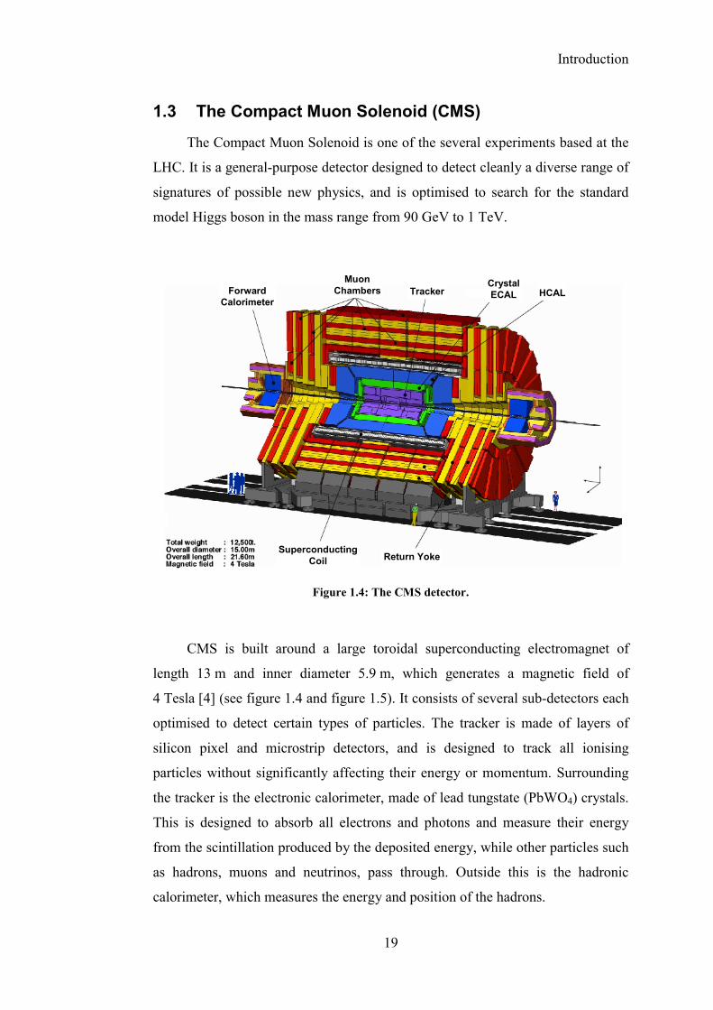
1.3 The Compact Muon Solenoid (CMS)
The Compact Muon Solenoid is one of the several experiments based at the
LHC. It is a general-purpose detector designed to detect cleanly a diverse range of
signatures of possible new physics, and is optimised to search for the standard
model Higgs boson in the mass range from 90 GeV to 1 TeV.
CMS is built around a large toroidal superconducting electromagnet of
length 13 m and inner diameter 5.9 m, which generates a magnetic field of
4 Tesla [4] (see figure 1.4 and figure 1.5). It consists of several sub-detectors each
optimised to detect certain types of particles. The tracker is made of layers of
silicon pixel and microstrip detectors, and is designed to track all ionising
particles without significantly affecting their energy or momentum. Surrounding
the tracker is the electronic calorimeter, made of lead tungstate (PbWO4) crystals.
This is designed to absorb all electrons and photons and measure their energy
from the scintillation produced by the deposited energy, while other particles such
as hadrons, muons and neutrinos, pass through. Outside this is the hadronic
calorimeter, which measures the energy and position of the hadrons.
ForwardCalorimeter
MuonChambers Tracker
CrystalECAL HCAL
SuperconductingCoil Return Yoke
Figure 1.4: The CMS detector.

Introduction
20
The only particles that escape through all these layers of detectors and the
magnet are muons and neutrinos. Muons lose energy almost solely through
ionisation along their path, and even in dense materials like steel or copper, this
amounts to a loss of only 1 MeV per millimetre. The muons are detected by the
muon chambers surrounding the detector, and the neutrinos have to be inferred
from missing energy.
1.3.1 The Magnet
The CMS magnet system consists of a large superconducting coil capable of
generating a magnetic field of 4 Tesla, and a return yoke to contain the generated
magnetic field. With a length of 13 m and an inner diameter of 5.9 m, it will be
the largest superconducting magnet in the world; the stored energy (2.5 GJ) is
Figure 1.5: Transverse view of the CMS detector.
Introduction
21
enough to melt 18 tonnes of gold. The use of such a high magnetic field allows a
much more efficient first-level trigger [5] by improving the momentum resolution
of the muon detectors. It also improves the momentum resolution of the tracker,
and allows the electromagnetic calorimeter to be accurately calibrated by
comparing the energies of electrons with their momentum in the tracker. A
reduction of the magnetic field strength to 3 Tesla, would require the running time
to increase by one third to achieve the same level of significance for a mass
measurement from multi-charged particle states [5].
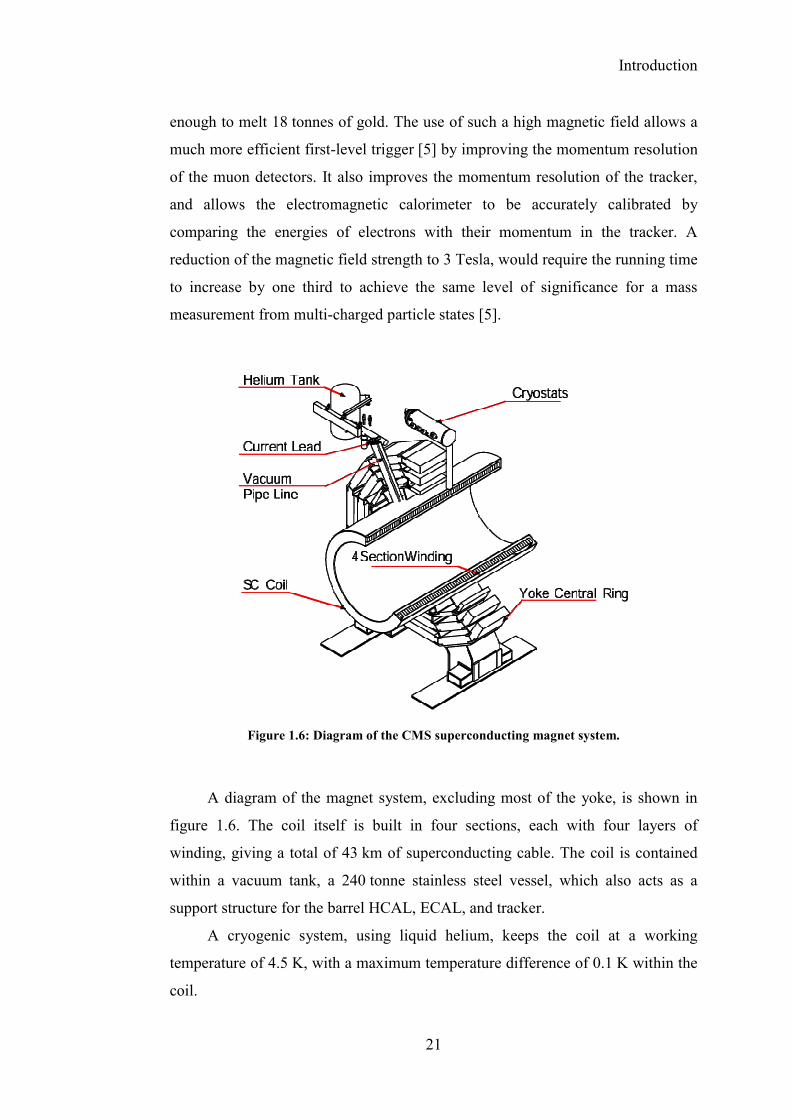
A diagram of the magnet system, excluding most of the yoke, is shown in
figure 1.6. The coil itself is built in four sections, each with four layers of
winding, giving a total of 43 km of superconducting cable. The coil is contained
within a vacuum tank, a 240 tonne stainless steel vessel, which also acts as a
support structure for the barrel HCAL, ECAL, and tracker.
A cryogenic system, using liquid helium, keeps the coil at a working
temperature of 4.5 K, with a maximum temperature difference of 0.1 K within the
coil.
Figure 1.6: Diagram of the CMS superconducting magnet system.

Introduction
22
1.3.2 The Tracker
The tracker is designed to reconstruct tracks efficiently, giving accurate
measurements of the vertex, the impact parameter, and any secondary vertices,
whilst being as thin as possible to minimise multiple scattering and energy loss,
which would have adverse effects on the calorimetry. It must have a high enough
spatial resolution to isolate and identify isolated leptons and photons, in order to
reduce backgrounds sufficiently for Higgs and SUSY searches. For a typical
particle energy of 100 GeV, the tracker can measure the transverse momentum
with a resolution of about 2 % up to |η| < 1.6 and about 6.5 % up to |η| < 2.5 [6].
The layout of the tracker is shown in figure 1.7. The central three layers are
based on silicon pixel detectors. Surrounding this is the inner barrel, consisting of
four layers of microstrip detectors, and the outer barrel, consisting of six layers.
At each end of the cylinder are the pixel forward detector (2 layers, pixel), the
inner disk (3 layers, microstrip) and the endcaps (9 layers). The original proposal
had been to use microstrip gas chambers (MSGCs) for the outer layers of the
tracker, but a review in December 1999 decided to move to an all-silicon design
as this was just as viable and allowed more effort to be concentrated onto a
smaller set of problems [7].
Figure 1.7: The CMS tracker.

Introduction
23
Pixel Detectors
The pixel detectors are located close to the interaction point, where the
occupancies are highest, in three barrel-layers and two end-layers. Each pixel
measures 150 x 150 µm, and by using charge sharing between pixels to interpolate
the track positions, will provide a spatial resolution of about 10 µm in the r-φ
direction and about 20 µm in the z direction [6]. The pixel detector will confirm or
reject track segments proposed by the surrounding tracker layers.
Microstrip Detectors
The microstrip detectors are arranged in 10 layers around the pixel
detectors. Their pitch varies from 80 µm in the inner layer to 205 µm in the outer
layer. Typical spatial resolutions (for a 100 µm pitch detector) are 34 µm in r-φ
and 320 µm in the z direction [6]. One of the prototype detector hybrid modules
from the microstrip tracker is shown in figure 1.8. It consists of two microstrip
detectors, bonded together at the centre. A pitch adaptor connects one end of the
detector to the APV readout chips. There is space for six APV chips; each reading
out 128 of the 768 detector strips, although in the prototype only three are
mounted, and only half of the detector is read out. A kapton cable connects the
outputs of the APVs to the opto-hybrid, where the signals are driven via optical
fibres to the counting room.
Figure 1.8: A prototype microstrip detector module from the tracker.
Introduction
24
1.3.3 The Electronic Calorimeter (ECAL)
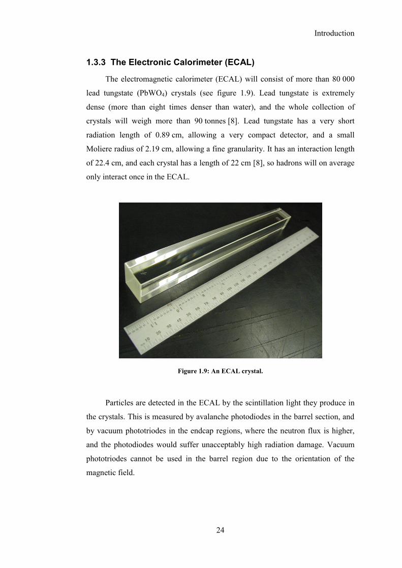
The electromagnetic calorimeter (ECAL) will consist of more than 80 000
lead tungstate (PbWO4) crystals (see figure 1.9). Lead tungstate is extremely
dense (more than eight times denser than water), and the whole collection of
crystals will weigh more than 90 tonnes [8]. Lead tungstate has a very short
radiation length of 0.89 cm, allowing a very compact detector, and a small
Moliere radius of 2.19 cm, allowing a fine granularity. It has an interaction length
of 22.4 cm, and each crystal has a length of 22 cm [8], so hadrons will on average
only interact once in the ECAL.
Particles are detected in the ECAL by the scintillation light they produce in
the crystals. This is measured by avalanche photodiodes in the barrel section, and
by vacuum phototriodes in the endcap regions, where the neutron flux is higher,
and the photodiodes would suffer unacceptably high radiation damage. Vacuum
phototriodes cannot be used in the barrel region due to the orientation of the
magnetic field.
Figure 1.9: An ECAL crystal.

Introduction
25
1.3.4 The Hadronic Calorimeter (HCAL)
The combined calorimeter system of CMS will measure the directions and
energies of quarks, gluons, and neutrinos indirectly by measuring the direction
and energy of particle jets and of the missing transverse energy [9]. Both the
barrel and the endcap of the HCAL (see figure 1.10) will experience the 4 Tesla
magnetic field of the CMS solenoid, and are therefore constructed from brass and
stainless steel, which are non-magnetic. The central hadronic calorimeter consists
of 4 mm thick plastic scintillator tiles inserted between copper absorber plates
(5 cm thick in the barrel and 8 cm thick in the endcaps). The scintillator tiles are
read out using wavelength-shifting plastic fibres. An additional layer of
scintillator tiles is located outside of the solenoid to ensure adequate sampling
depth for the whole |η| < 3 region. This is known as the outer hadronic
calorimeter. The thickness of the HCAL system varies from 5.15 interaction
lengths at η = 0 up to 5.82 interaction lengths [9].
Figure 1.10: An assembled half-barrel of the HCAL.
Introduction
26
The HCAL also includes the forward calorimeter, located 6 m downstream
from the HCAL endcaps, and extending the hermeticity of the hadronic
calorimeter up to |η| < 5. It is constructed from quartz fibres embedded in a copper
absorber matrix, and is necessary for an accurate measurement of missing
transverse energy, and for forward jet detection.
1.3.5 The Muon Detectors
There are three different types of detector used for muons: Resistive Parallel
Plate Chambers (RPCs), Drift Tubes (DTs), and Cathode Strip Chambers (CSCs).
Together they measure the transverse momentum of the muons with an accuracy
of better than 4 % up to |η| < 2, for muons with a typical energy of 100 GeV [10].
Drift Tubes
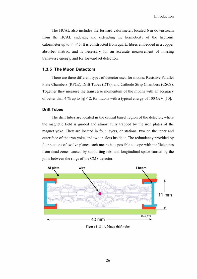
The drift tubes are located in the central barrel region of the detector, where
the magnetic field is guided and almost fully trapped by the iron plates of the
magnet yoke. They are located in four layers, or stations; two on the inner and
outer face of the iron yoke, and two in slots inside it. The redundancy provided by
four stations of twelve planes each means it is possible to cope with inefficiencies
from dead zones caused by supporting ribs and longitudinal space caused by the
joins between the rings of the CMS detector.
Al plate I-beamwire
Figure 1.11: A Muon drift tube.
Introduction
27
A diagram of a drift tube is shown in figure 1.11. It consists of parallel
aluminium plates separated by aluminium I-beams, with a wire stretched along the
centre. When an ionising particle passes through the tube, it liberates electrons,
which then drift along the electric field lines towards the positively charged wire.
The time taken for the ionisation electrons to drift to the wire is measured to
within an accuracy of 1 ns, and as the drift velocity of the electrons is known, this
gives a good measure of the distance of the original particle from the wire.
Cathode Strip Chambers
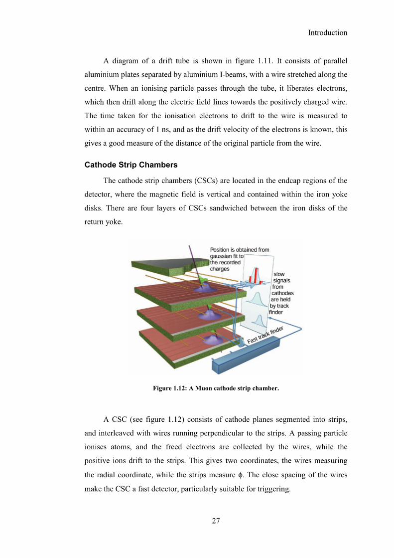
The cathode strip chambers (CSCs) are located in the endcap regions of the
detector, where the magnetic field is vertical and contained within the iron yoke
disks. There are four layers of CSCs sandwiched between the iron disks of the
return yoke.
A CSC (see figure 1.12) consists of cathode planes segmented into strips,
and interleaved with wires running perpendicular to the strips. A passing particle
ionises atoms, and the freed electrons are collected by the wires, while the
positive ions drift to the strips. This gives two coordinates, the wires measuring
the radial coordinate, while the strips measure φ. The close spacing of the wires
make the CSC a fast detector, particularly suitable for triggering.
Figure 1.12: A Muon cathode strip chamber.
Introduction
28
Resistive Parallel Plate Chambers
The Resistive Plate Chambers (RPCs) are used in both the barrel and the
endcap regions of the detector, and are used to provide an additional
complementary trigger. They will cover approximately the same area as the DTs
and CSCs, but will provide a faster timing signal and have a different sensitivity
to background.
An RPC is shown in figure 1.13. It consists of two parallel plates of high-
resistivity plastic material, separating a thin gap filled with gas. A passing ionising
particle releases electrons, which accelerate towards the positively charged side of
the chamber in an avalanche. The plastic is transparent to these electrical signals,
which are then picked up by external metallic strips.
The signals from each of the three types of muon detectors proceed in
parallel to the trigger logic. Every muon with enough energy to penetrate the
detector material should traverse at least three of the muon stations.
1.3.6 The Trigger
In normal operation, the global trigger processor receives data from the
calorimeters and the muon chambers. It can also use special signals for set-up,
synchronisation, calibration and testing purposes. It contains logic for processing
up to 128 different trigger algorithms in parallel, the results being delivered as a
Figure 1.13: A Muon resistive plate chamber.
Introduction
29
128-bit word, with one bit per algorithm. This can be compared with a predefined
input word that selects which particular triggers are of interest for the run.
The level-1 accept trigger decision (L1A), along with the 40.08 MHz LHC
machine clock, and other signals, such as bunch-crossing reset are distributed to
the detector by the TTC system. The data for each 25 ns bunch-crossing period
are stored in the detector front-end until the trigger decision is known. This
period, known as the trigger latency, will be about 3 µs.
1.4 Summary
The CMS detector and its readout system need to process huge volumes of
data, and reduce it to a manageable amount before it can be stored and properly
analysed. The LHC, at its full luminosity, will generate 20 interactions with a
significant transverse energy for every bunch crossing, at a rate of 40.08 MHz.
The first level trigger will reduce this to a rate of up to 100 kHz, with the raw data
for each event being about 1 Mbyte. This means that the readout system still
needs to process about 100 Gbyte of data every second. The tracker consists of
about 10 million detector channels, and is expected to generate up to 70 % of the
final data volume at CMS. These data rates are orders of magnitude higher than in
any previous experiment and demand state-of-the-art technology as well as
massively parallel processing if the experiment is to be successful.
Figure 1.14: The CMS level-1 global trigger.
(Adapted from ref [11])

30
Chapter 2: Field Programmable Devices All digital logic circuits are made up of simple building blocks known as
logic gates, which are in turn made of transistors. Two main technologies exist,
known as transistor-transistor logic (TTL) and complementary metal oxide
semiconductor (CMOS).
2.1 Digital Logic
The older of the two, TTL is made of bipolar transistors, which are
sandwiches of n- and p-type semiconductor material in either npn or pnp
configurations (see figure 2.1). The transistor consists of two p-n junctions, with
the thin central section connected to the base terminal, and the two ends connected
to the collector and the emitter. An npn transistor conducts current when its base
is pulled high, and a pnp transistor conducts when its base is low. Bipolar
transistors are current-amplifying devices: the amount of current flowing into the
base controls the amount of current flowing in the collector circuit, but they can
also be used in voltage amplification circuits. Bipolar transistors can operate at
speeds in excess of a gigahertz, and can be designed to handle large currents up to
several amps, but they have a relatively low input impedance of up to about 1 kΩ,
and so are not suitable for applications requiring high circuit impedance.
N N NP P P
Base Base
Emitter EmitterCollector Collector
B B
C C
E E
Characteristic Curves for 2N3904 (NPN)
IB = 10 µA
IB = 80 µA
VCE (V)
I C(A
)
Figure 2.1: Bipolar transistors (npn and pnp) and their symbols.
Field Programmable Devices
31
Field effect transistors exist in two main types, Junction Field Effect
Transistor (JFET) and Metal Oxide Semiconductor FET (MOSFET). In both
types, current flows along a semiconductor channel (n-type or p-type) between the
source at one end and the drain at the other. In a JFET, the gate is of the opposite
type of semiconductor to the channel, creating a p-n junction (see figure 2.2). A
DC voltage is connected to the gate so that the junction is normally reverse-
biased, although under certain conditions a small current can flow during part of
the signal cycle.
In MOSFETs the gate electrode is a piece of metal, separated from the
semiconductor by a layer of oxidised silicon (see figure 2.3). This gate oxide acts
as a dielectric and electrically insulates the gate from the junction. Because of this,
the MOSFET has a very high input impedance of several megohms, and virtually
no current flows during any part of the input cycle. However, the oxide layer is
very thin, and is susceptible to damage from electrostatic discharge, so special
precautions are necessary when handling MOS devices. A p-channel FET
conducts when the gate voltage is low, and an n-channel FET conducts when the
gate voltage is high.
Source DrainGate
Bulk
SubstrateTerminal
p-n+ n+
n-p
Source DrainGate
SubstrateTerminal
n-p+ p+
p-n
G
D
S
G
D
S
Characteristic Curves for a Typical JFET
VDS (V)
I D(m
A)
VG = 0 V
VG = 2 V
VG = 1 V
Figure 2.2: JFET transistors (n-channel and p-channel) and their symbols.
Field Programmable Devices
32
The dominant semiconductor technology is CMOS, which uses a
combination of both n-channel and p-channel MOSFETS. The main advantage is
its very low static power consumption; power is only dissipated when the circuit
switches, allowing many gates to be integrated into each IC, resulting in higher
performance than is possible with bipolar technology.
2.1.1 Combinatorial Logic
A CMOS inverter can be built with only two complementary MOSFET
transistors (see figure 2.4). When the input voltage is high, the output is connected
Source Drain
Gate
Bulk
SiO2
p-n+ n+
Source Drain
Gate
SiO2
n-p+ p+
SubstrateTerminal (B)
SubstrateTerminal (B)
Metal Metal
G
D
S
BG
D
S
G
D
S
BG
D
S
Figure 2.3: MOSFET transistors (n-channel and p-channel) and their symbols.
VDD
GND
A Q A Q
S
S’
A Q A Q
S
S’
Figure 2.4: A CMOS inverter and transmission gate, and their symbols.

Field Programmable Devices
33
to ground, and when it is low, the output is connected to the drain voltage, VDD
(typically 1.8, 2.5, 3.3 or 5V). A transmission gate is used like a switch; when the
input S is high (and S' is low), the input A appears at the output Q, and when S is
low (and S' is high), the output is in a high impedance state, effectively
disconnected.
Two other combinatorial logic gates, the NAND and the NOR, are shown in
figure 2.5, along with their truth tables in table 2.1. Other logic gates, such as
AND and OR gates can be easily constructed by following the output of a NAND
or NOR gate with an inverter.
VDD
GND
A Q
B
VDD
GND
A
Q
B
Figure 2.5: CMOS NAND and NOR gates and their symbols.
A B Q A B Q 0 0 1 0 0 1 0 1 1 0 1 0 1 0 1 1 0 0 1 1 0 1 1 0
Table 2.1: Truth tables for NAND and NOR gates.
Field Programmable Devices
34
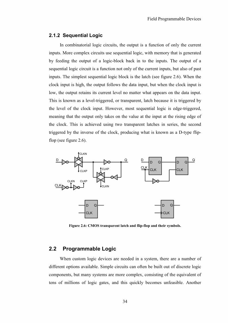
2.1.2 Sequential Logic
In combinatorial logic circuits, the output is a function of only the current
inputs. More complex circuits use sequential logic, with memory that is generated
by feeding the output of a logic-block back in to the inputs. The output of a
sequential logic circuit is a function not only of the current inputs, but also of past
inputs. The simplest sequential logic block is the latch (see figure 2.6). When the
clock input is high, the output follows the data input, but when the clock input is
low, the output retains its current level no matter what appears on the data input.
This is known as a level-triggered, or transparent, latch because it is triggered by
the level of the clock input. However, most sequential logic is edge-triggered,
meaning that the output only takes on the value at the input at the rising edge of
the clock. This is achieved using two transparent latches in series, the second
triggered by the inverse of the clock, producing what is known as a D-type flip-
flop (see figure 2.6).
2.2 Programmable Logic
When custom logic devices are needed in a system, there are a number of
different options available. Simple circuits can often be built out of discrete logic
components, but many systems are more complex, consisting of the equivalent of
tens of millions of logic gates, and this quickly becomes unfeasible. Another
D Q
CLKN
CLKN
CLKPCLKP
CLKCLKN CLKP
D
CLK
Q
D
CLK
Q D
CLK
Q
D
CLK
Q
D Q
CLK
Figure 2.6: CMOS transparent latch and flip-flop and their symbols.
Field Programmable Devices
35
option is to use a microprocessor, which offers great flexibility and is functionally
very versatile, but due to its inherently serialised processing, for many tasks it is
just too slow, when compared to the hugely parallel processing available in a
dedicated logic circuit.
Application-specific integrated circuits (ASICs) are made up of successive
layers, etched directly onto a silicon wafer using a photographic mask, and offer
the highest level of complexity and speed. In full-custom ASICs, all mask layers
are customised, and designing a new IC takes a huge amount of time and effort, as
each individual transistor needs to be specified. In a standard-cell-based ASIC all
layers are also customised, but a library of standard cells are available for higher-
level functions, reducing the design effort to some extent. Another type of ASIC
technology is the mask-programmable gate array (MPGA), which consists of an
array of standard blocks, with only the interconnect layers being customised [12].
This reduces the manufacturing lead-time, but any design changes still require a
complete new manufacturing run.
Field programmable logic devices have no custom mask layers or custom
logic cells; they are programmed by the user. They have the advantage over
custom-designed ASICs that the design and verification process is much faster,
and (in technologies which are not one-time programmable) the configuration can
be updated at a later time to fix errors, or simply to upgrade the firmware. For
small to medium volumes they are also much cheaper. The disadvantage is that all
the programming logic takes up space in the chip, leaving less space for the actual
design. In a 0.18µm process an FPGA typically holds 1500 gates/mm2 compared
to 60 000 gates/mm2 for an ASIC, and runs at a maximum clock speed of
100 MHz, compared to 600 MHz in an ASIC. However, the density of these
devices is increasing rapidly, and in many situations it is the speed of the
input/output logic that limits the amount of processing that can be done, so
FPGAs are becoming powerful enough to replace ASICs in more and more
situations.

Field Programmable Devices
36
2.3 History of Programmable Logic
2.3.1 The PROM
The first type of user-programmable chip that could implement logic
circuits was the PROM [13] (see figure 2.7). The n address lines represent the
input to the logic function, the decoder translates each of the 2n possible
combinations to a logic signal on one of 2n lines, and the m data lines are different
functions of the inputs. Filling the memory appropriately allows any arbitrary
logic function to be generated [12]. The 2n lines generated by the decoder are
known as product terms, and are logical ANDs of the input lines (or their
inverses). If each product term is a function of all of the input lines (or their
inverses), as is the case here, then they are known more specifically as minterms,
and each will be active for only one possible input combination. Each function is
simply a logical OR of all the minterms for which the corresponding bit in the
memory is high. This method of representing a logic function is known as a sum
of products (SOP).
Decoder
PROM
12
n
2n
Address
Data1 2 m
Decoder
PROM
12
n
2n
Address
Data1 2 m
Figure 2.7: Memory used as programmable logic.
(Adapted from ref [13])
Field Programmable Devices
37
2.3.2 The PLA and PAL
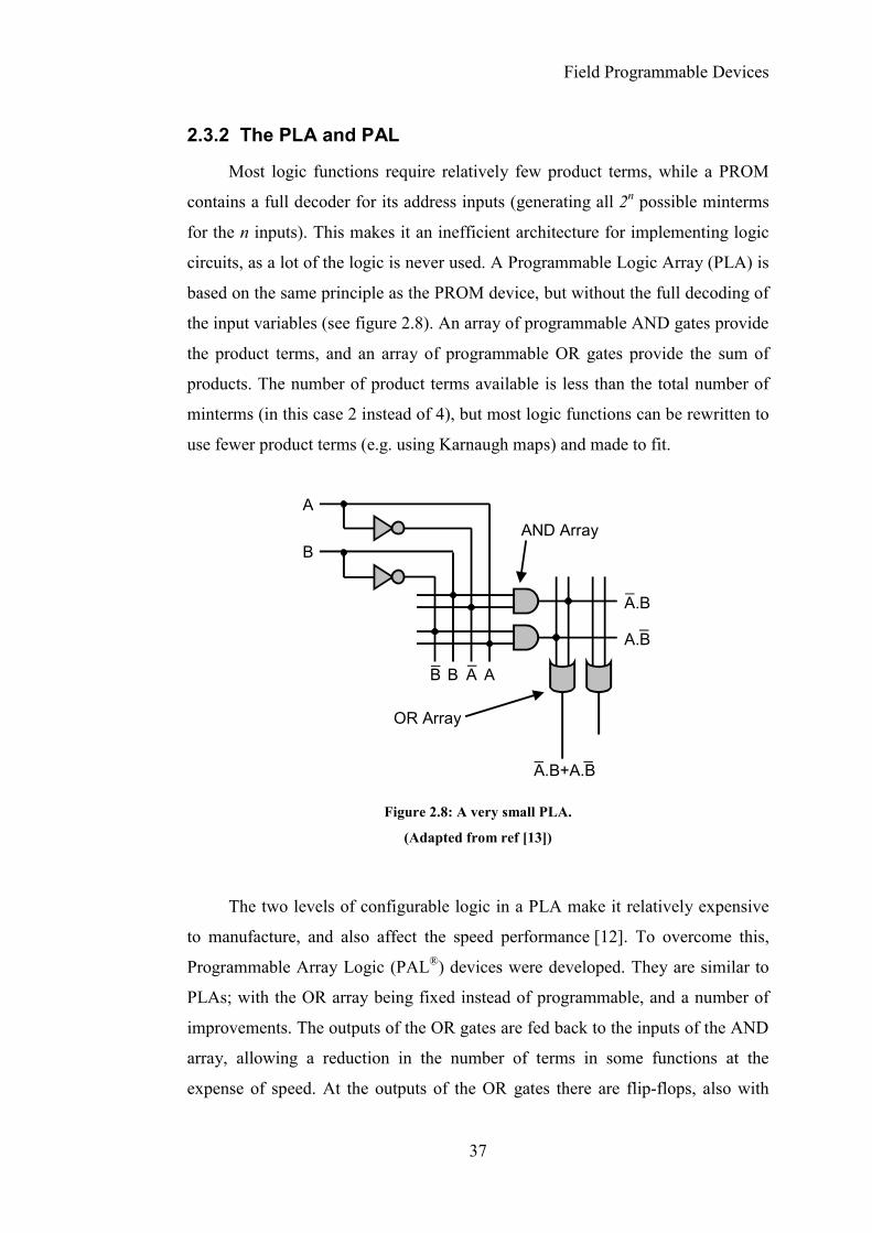
Most logic functions require relatively few product terms, while a PROM
contains a full decoder for its address inputs (generating all 2n possible minterms
for the n inputs). This makes it an inefficient architecture for implementing logic
circuits, as a lot of the logic is never used. A Programmable Logic Array (PLA) is
based on the same principle as the PROM device, but without the full decoding of
the input variables (see figure 2.8). An array of programmable AND gates provide
the product terms, and an array of programmable OR gates provide the sum of
products. The number of product terms available is less than the total number of
minterms (in this case 2 instead of 4), but most logic functions can be rewritten to
use fewer product terms (e.g. using Karnaugh maps) and made to fit.
The two levels of configurable logic in a PLA make it relatively expensive
to manufacture, and also affect the speed performance [12]. To overcome this,
Programmable Array Logic (PAL®) devices were developed. They are similar to
PLAs; with the OR array being fixed instead of programmable, and a number of
improvements. The outputs of the OR gates are fed back to the inputs of the AND
array, allowing a reduction in the number of terms in some functions at the
expense of speed. At the outputs of the OR gates there are flip-flops, also with
A
B
B B A A_ _
A.B
A.B
_
_
A.B+A.B_ _
AND Array
OR Array
Figure 2.8: A very small PLA.
(Adapted from ref [13])
Field Programmable Devices
38
their outputs fed back to the inputs of the AND array, allowing more complex
systems to be built, such as state machines. The I/O pins are programmable, with
tri-state outputs, allowing them to be used for input, output, or bi-directional
signals.
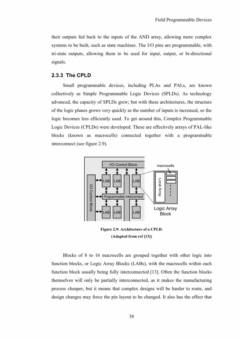
2.3.3 The CPLD
Small programmable devices, including PLAs and PALs, are known
collectively as Simple Programmable Logic Devices (SPLDs). As technology
advanced, the capacity of SPLDs grew; but with these architectures, the structure
of the logic planes grows very quickly as the number of inputs is increased, so the
logic becomes less efficiently used. To get around this, Complex Programmable
Logic Devices (CPLDs) were developed. These are effectively arrays of PAL-like
blocks (known as macrocells) connected together with a programmable
interconnect (see figure 2.9).
Blocks of 8 to 16 macrocells are grouped together with other logic into
function blocks, or Logic Array Blocks (LABs), with the macrocells within each
function block usually being fully interconnected [13]. Often the function blocks
themselves will only be partially interconnected, as it makes the manufacturing
process cheaper, but it means that complex designs will be harder to route, and
design changes may force the pin layout to be changed. It also has the effect that
LAB
Local Array
macrocells
Logic ArrayBlock
LAB LAB
LAB LAB LAB
I/O C
ontrol Block
Programmable Interconnect
I/O Control Block
Programmable Interconnect
I/O C
ontrol Block
Figure 2.9: Architecture of a CPLD.
(Adapted from ref [13])
Field Programmable Devices
39
the delays between the function blocks are not fixed, whereas with full
interconnect the delays are fixed and predictable.
CPLDs are generally CMOS devices, and use non-volatile memory cells
(usually EEPROM or FLASH) to define their functionality. Typically, they are in-
system programmable (ISP), meaning they can be programmed in-circuit, as
opposed to needing to be plugged into a special CPLD-programming unit.
2.3.4 The FPGA
The architecture of CPLDs makes it difficult to increase the capacity beyond
the equivalent of about 50 SPLD devices. The highest capacity devices, Field
Programmable Gate Arrays (FPGAs), are based on a different architecture, similar
to MPGAs. They are made up of an array of up to about 100 000 configurable
logic blocks (CLBs), surrounded by programmable I/O blocks, and connected by
a programmable interconnect network (see figure 2.10). The blocks are not fully
interconnected, but sophisticated software is used to route the logic.
FPGAs can be either coarse-grained or fine-grained. Coarse-grained FPGAs
contain large logic blocks containing two or more look-up tables, two or more
flip-flops, and other logic such as multiplexers and fast-carry logic. Fine-grained
FPGAs, on the other hand, contain a large number of simple logic blocks
containing either a 2-input logic function or 4-to-1 multiplexer, and a flip-flop.
They make more efficient use of the active components, but require greater
CLB
IOB
CLB
IOB
IOB
I/O Block
ConfigurableLogic Block
Switch Matrix
Figure 2.10: Architecture of an FPGA.
(Adapted from ref [13])

Field Programmable Devices
40
routing resources, and are generally slower and less dense. An example (from a
Plessey device) is shown in figure 2.11.
2.4 Memory Technology
2.4.1 Fuses and Antifuses
Field programmable devices are programmed after the manufacturing
process, and the configuration has to be stored in some form of memory. There
are several technologies available for this, each with its own advantages and
disadvantages. The original technology used was fuse technology. A metal link
creates a normally closed connection, and the device is programmed by passing a
relatively large current through the fuse, melting it and opening the connection.
ConfigurationRAM
Clk
D QMux8x2
Latch
InterconnectLines
Figure 2.11: Example of a fine-grained logic cell.
(Adapted from ref [13])
~20 nm
<10 nm
Poly-Si
ONO dielectric
n+
antifuse link antifuse link
metal 2
metal 1
SiO2
amorphous Si
Figure 2.12: Antifuses: (a) ONO, (b) amorphous silicon.
(Adapted from ref [13])

Field Programmable Devices
41
A variation of this is antifuse technology; it is now much more widely
employed as it uses a modified CMOS technology. An oxide-nitride-oxide (ONO)
antifuse (see figure 2.12a) consists of an insulating ONO layer sandwiched
between conductive polysilicon and n+ diffusion layers [13, 14]. The device is
programmed by applying a current of 5-15 mA, causing the thin dielectric to melt,
and form a small antifuse link with a typical resistance of about 500 Ω, and
allowing current to flow through the device. The amorphous silicon (or metal-
metal) antifuse (see figure 2.12b) is similar to the ONO variety, with the
advantages that the connections are made directly to metal; they have a lower
programmed resistance (typically about 80 Ω), and have less parasitic
capacitance. Antifuses are small and radiation hard, but they are slow to program,
cannot be reprogrammed, and their properties can vary over time, creating
reliability issues.
2.4.2 The EPROM and EEPROM
Another technology used is the EPROM, which is only slightly larger than
an antifuse. It is similar to a standard n-channel MOSFET, with an extra floating
gate (see figure 2.13a). In normal operation, the floating gate has no charge and
the field effect transistor can be switched on or off by the gate voltage. To
program the device, VDS is set to a large voltage (~12 V) creating energetic, or hot,
electrons in the bulk. The gate voltage VGS is set to a positive voltage, attracting
some of the electrons, which tunnel through the gate oxide and are trapped in the
floating gate, producing a negative charge. This increases the threshold voltage
n+
S D
G
floating gate
Bulk
gate oxide
input wires
product wire
VDD
VGS
VDS
Figure 2.13: An EPROM memory cell: a) schematic, b) use in wired-AND.
(Adapted from ref [13] (a) and ref [12] (b))

Field Programmable Devices
42
enough so that the transistor is then permanently switched off, even with a
positive gate voltage up to VDD. An EPROM cell can be used in a programmable
AND-plane (see figure 2.13b) where each input wire is connected to a separate
EPROM cell and can be disabled by programming the relevant cell. If the device
is built with a UV-transparent window, it can be erased by being exposed to UV
light. This gives the trapped electrons enough energy to return to the substrate,
therefore erasing the program; although it requires about an hour of exposure
before the device is completely erased, and cannot be done in-circuit.
An EEPROM (or E2PROM) is similar to an EPROM, but uses an electric
field to remove the trapped electrons, allowing this to be done in-circuit. Because
of this, the cells are generally about twice as large as those in an EPROM. Some
newer devices use FLASH memory, which is a type of EEPROM, but the electric
field is applied to large areas of the memory at once so the erase time is much
shorter, and the cells are smaller, being only slightly larger than in an EPROM.
2.4.3 SRAM
Many devices use static RAM (SRAM) technology (see figure 2.14). SRAM
cells are relatively large, and are volatile, so any program will be lost when the
power is removed. However, most SRAM devices are in-system programmable,
and are designed to automatically boot at power-up from a PROM, which
typically takes no more than a few hundred milliseconds. SRAM is widely used in
FPGAs, where the function generators are often implemented as look-up tables. In
this way, the tables can be made writeable and therefore used as memory blocks
as well as function generators.
D
Write
Q_
Q
Figure 2.14: An SRAM memory cell.
(Adapted from refs [13, 15])
Field Programmable Devices
43
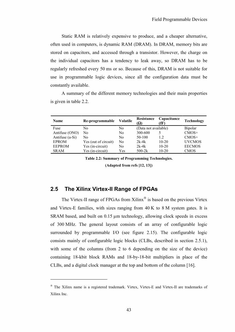
Static RAM is relatively expensive to produce, and a cheaper alternative,
often used in computers, is dynamic RAM (DRAM). In DRAM, memory bits are
stored on capacitors, and accessed through a transistor. However, the charge on
the individual capacitors has a tendency to leak away, so DRAM has to be
regularly refreshed every 50 ms or so. Because of this, DRAM is not suitable for
use in programmable logic devices, since all the configuration data must be
constantly available.
A summary of the different memory technologies and their main properties
is given in table 2.2.
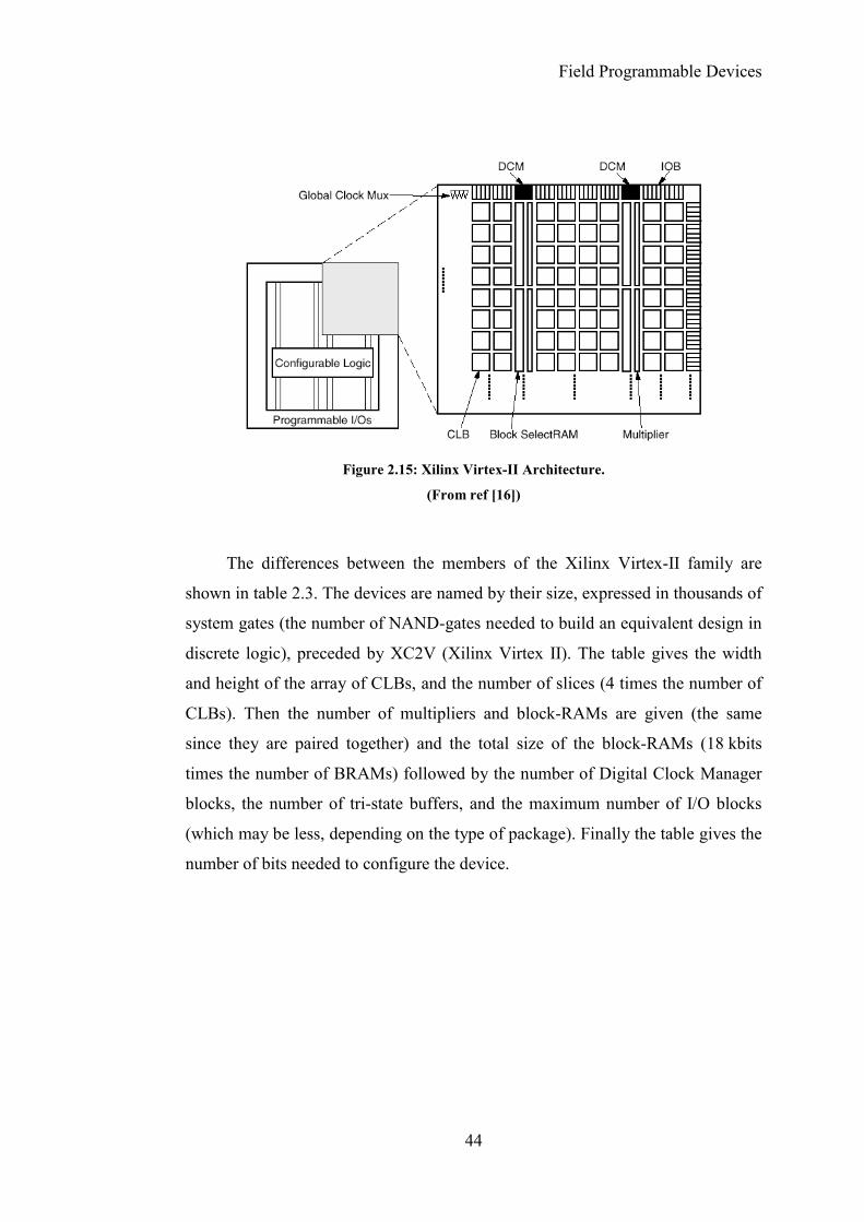
2.5 The Xilinx Virtex-II Range of FPGAs
The Virtex-II range of FPGAs from Xilinx is based on the previous Virtex
and Virtex-E families, with sizes ranging from 40 K to 8 M system gates. It is
SRAM based, and built on 0.15 µm technology, allowing clock speeds in excess
of 300 MHz. The general layout consists of an array of configurable logic
surrounded by programmable I/O (see figure 2.15). The configurable logic
consists mainly of configurable logic blocks (CLBs, described in section 2.5.1),
with some of the columns (from 2 to 6 depending on the size of the device)
containing 18-kbit block RAMs and 18-by-18-bit multipliers in place of the
CLBs, and a digital clock manager at the top and bottom of the column [16].
The Xilinx name is a registered trademark. Virtex, Virtex-E and Virtex-II are trademarks of
Xilinx Inc.
Name Re-programmable Volatile Resistance (Ω)
Capacitance (fF) Technology
Fuse No No (Data not available) Bipolar Antifuse (ONO) No No 300-600 5 CMOS+ Antifuse (a-Si) No No 50-100 1.2 CMOS+ EPROM Yes (out of circuit) No 2k-4k 10-20 UVCMOS EEPROM Yes (in-circuit) No 2k-4k 10-20 EECMOS SRAM Yes (in-circuit) Yes 500-2k 10-20 CMOS
Table 2.2: Summary of Programming Technologies.
(Adapted from refs [12, 13])
Field Programmable Devices
44
The differences between the members of the Xilinx Virtex-II family are
shown in table 2.3. The devices are named by their size, expressed in thousands of
system gates (the number of NAND-gates needed to build an equivalent design in
discrete logic), preceded by XC2V (Xilinx Virtex II). The table gives the width
and height of the array of CLBs, and the number of slices (4 times the number of
CLBs). Then the number of multipliers and block-RAMs are given (the same
since they are paired together) and the total size of the block-RAMs (18 kbits
times the number of BRAMs) followed by the number of Digital Clock Manager
blocks, the number of tri-state buffers, and the maximum number of I/O blocks
(which may be less, depending on the type of package). Finally the table gives the
number of bits needed to configure the device.
Figure 2.15: Xilinx Virtex-II Architecture.
(From ref [16])
Field Programmable Devices
45
2.5.1 Logic Blocks
In the Xilinx Virtex-II FPGA family, each CLB contains four similar slices
(see figure 2.16a) arranged in two columns with separate carry chains (used for
implementing arithmetic functions and sum of products logic) and a single shift
chain (used for implementing shift registers). There are also two tristate buffers
Device CLB Array Slices
Multipliers/BRAMs
BRAM(kbits) DCMs
3-State Buffers
Max. IOBs
Config. Bits
XC2V40 8 x 8 256 4 72 4 128 88 338 208 XC2V80 16 x 8 512 8 144 4 256 120 597 408 XC2V250 24 x 16 1 536 24 432 8 768 200 1 591 584 XC2V500 32 x 24 3 072 32 576 8 1 536 264 2 557 856 XC2V1000 40 x 32 5 120 40 720 8 2 560 432 3 749 408 XC2V1500 48 x 40 7 680 48 864 8 3 840 528 5 166 240 XC2V2000 56 x 48 10 752 56 1 008 8 5 376 624 6 808 352 XC2V3000 64 x 56 14 336 96 1 728 12 7 168 720 9 589 408 XC2V4000 80 x 72 23 040 120 2 160 12 11 520 912 14 220 192XC2V6000 96 x 88 33 792 144 2 592 12 16 896 1 104 19 752 096XC2V8000 112 x 104 46 592 168 3 024 12 23 296 1 108 26 185 120XC2V10000 128 x 120 61 440 192 3 456 12 30 720 1 108 33 519 264
Table 2.3: Virtex-II family members.
(Adapted from ref [17])
Figure 2.16: Virtex-II logic blocks: (a) CLB, (b) slice.
(From ref [17])
Field Programmable Devices
46
which are accessible to any of the slices via the switch matrix [17]. Each slice (see
figure 2.16b) contains:
• Two independent function generators, implemented as 4-input look-up
tables (LUT F and G), which can be reconfigured as 16x1-bit RAMs
(RAM16) or 16-bit variable-tap shift registers (SRL16). If used as RAM, the
look-up tables in a CLB can be combined into a larger memory blocks, from
16x8-bit to 128x1-bit. When used as shift-registers, the slices can be
combined into one long 128-bit shift-register with dynamic access to any bit
in the chain.
• Multiplexers (MUXF5 and MUXFx) to combine the outputs of the function
generators and produce functions with larger numbers of inputs. Along with
the function generators, MUXF5 can generate functions of five inputs, and
MUXFx can generate functions of 6, 7 or 8 inputs, depending on the slice in
the CLB.
• Logic for building fast carry chains (CY), used to build efficient addition
and subtraction logic.
• A dedicated OR gate (ORCY) connecting carry logic with the output of the
corresponding ORCY in the adjacent slice, allowing easy production of
large sum of products chains.
• Logic for other arithmetic functions, such as efficient multiplier
implementations.
• Two registers, configurable as either edge-triggered D-type flip-flops, or as
level-sensitive latches.
Depending on its size, each Virtex-II FPGA can have between 64 and
11 648 CLBs. On top of that, it can have up to 168 18-kbit dual-port block RAMs.
Each port of each block RAM can be individually configured for various widths
(see table 2.4). In the 9, 18 and 36-bit widths the full 18 kbits are accessible with
one bit per byte available for parity or for any other use. In the narrower
configurations, the parity bits are not available and only 16 kbits are accessible.
Field Programmable Devices
47
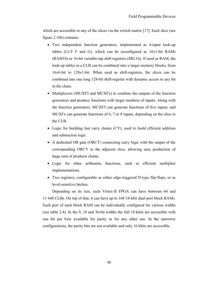
Associated with each block-RAM is an 18-bit twos-complement signed
multiplier. The switch matrix is optimised to feed one input from an 18-bit wide
block RAM, although they can be used separately. This is because many digital
signal-processing applications use a multiplier-accumulator function for finite and
infinite impulse response (FIR and IIR) digital filters.
Each FPGA has 16 clock inputs, and a number of global clock buffers used
to distribute the clocks to the synchronous logic elements. There are also up to 12
Digital Clock Managers (DCMs), which are based on delay-locked loops (DLLs).
Unlike phase-locked loops (PLLs) they are completely digital, meaning they are
less affected by temperature and supply voltage variations. However, PLLs
generally have lower jitter, as they tend to filter out higher frequency components.
The DCMs are used to de-skew the clock signals, ensuring that they remain in
phase over the whole device, and perform clock multiplication and division,
generating a wide range of clock frequencies from a single clock source.
2.5.2 I/O Blocks
Connections to the outside world are made through programmable
input/output blocks (IOBs). Each pin can be an input, an output, or bi-directional,
and neighbouring pairs of IOBs can be combined to provide differential
signalling [17]. Groups of IOBs are organised into eight banks (see figure 2.17a),
each of which can operate at a range of voltages from 1.2 to 3.3 Volts,
independently of the core voltage of 1.5 V; this allows a number of I/O signalling
standards to be supported while maintaining a low core voltage. The increasing
Width (bits) Depth (bits) Addressable bits 36 512 18 k 18 1 k 18 k 9 2 k 18 k 4 4 k 16 k 2 8 k 16 k 1 16 k 16 k
Table 2.4: Virtex-II block-RAM configurations.
(Adapted from ref [17])
Field Programmable Devices
48
density of FPGAs means that there is little space for termination resistors,
especially with ball grid array packages. To help with this, each bank contains a
digitally controlled impedance system, where a single pair of resistors provides a
reference to set the series and/or parallel termination resistance of the entire bank.
Each IOB (see figure 2.17b) contains six registers, each of which can be
configured as an edge-triggered D-type flip-flop or as a level-sensitive latch. Each
path (input, output, and 3-state) contains two of these registers, allowing double
data rate (DDR) input/output signals by clocking each register 180° out of phase
with respect to the other.
Figure 2.17: (a) I/O banks in Virtex-II flip-chip packages, (b) an I/O block.
(From ref [17])

Field Programmable Devices
49
2.5.3 Routing Resources
On top of the blocks mentioned, there are a number of local and global
routing resources used to connect the blocks together and distribute signals across
the device. Unlike previous architectures, the Virtex-II uses Active Interconnect
technology, where the signals are fully buffered at each routing interconnect
point. This means that signal delays are more precisely controlled and reasonably
independent of signal fan-out, making it easier to route complex designs [17].
Each CLB, DCM and IOB is connected to a switch matrix, and each block RAM
and multiplier share four switch matrices between them (see figure 2.18). Each
switch matrix provides eight fast connections from the outputs of the associated
block back to the inputs, and 16 direct connections to the eight neighbouring
blocks. There are 40 horizontal and 40 vertical double lines providing connections
to every first or second block away in all four directions, and 120 horizontal and
120 vertical hex lines providing connections to every third or sixth block. Finally
there are 24 horizontal and 24 vertical long lines which are bi-directional wires
spanning the width and height of the device. In addition to these routing resources
Figure 2.18: Virtex-II routing resources.
(From ref [17])
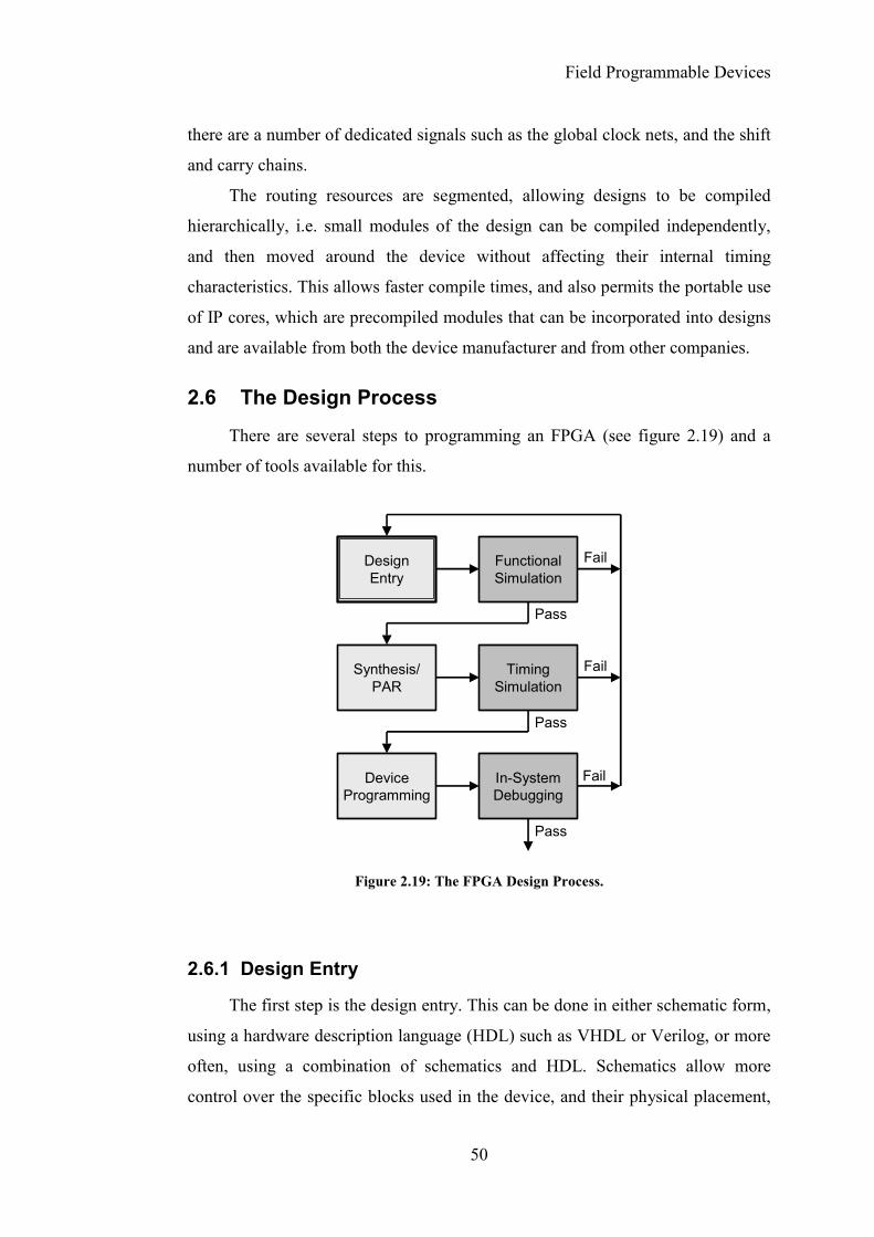
Field Programmable Devices
50
there are a number of dedicated signals such as the global clock nets, and the shift
and carry chains.
The routing resources are segmented, allowing designs to be compiled
hierarchically, i.e. small modules of the design can be compiled independently,
and then moved around the device without affecting their internal timing
characteristics. This allows faster compile times, and also permits the portable use
of IP cores, which are precompiled modules that can be incorporated into designs
and are available from both the device manufacturer and from other companies.
2.6 The Design Process
There are several steps to programming an FPGA (see figure 2.19) and a
number of tools available for this.
2.6.1 Design Entry
The first step is the design entry. This can be done in either schematic form,
using a hardware description language (HDL) such as VHDL or Verilog, or more
often, using a combination of schematics and HDL. Schematics allow more
control over the specific blocks used in the device, and their physical placement,
DesignEntry
FunctionalSimulation
TimingSimulation
In-SystemDebugging
Synthesis/PAR
DeviceProgramming
Fail
Fail
Fail
Pass
Pass
Pass
Figure 2.19: The FPGA Design Process.

Field Programmable Devices
51
although for complex designs this is also more time-consuming. Language-based
tools, on the other hand, allow quick design entry, especially for more
sophisticated designs. In the past, this was often at the expense of lower
performance or density; but logic synthesis tools have significantly improved over
recent years, and are becoming better at inferring the correct blocks to use for
different language constructs. Language-based tools also permit a higher level of
abstraction, making designs easier to port to different devices, but they also pose
dangers. For example, if a conditional statement (e.g. if or case) does not take into
account all possible input states, it will be assumed that the output should remain
unchanged in these cases. This implies memory (the signal must remember its
previous value) and therefore a latch is needed. This is useful if a latch is actually
required, but can often be unintentional, leading to code bloat (redundant logic
that increases the size of a design without adding any functionality).
Libraries are available from the hardware vendors for blocks that cannot
easily be inferred from an HDL. For example, in the Virtex-II, RAM is available
in several block-RAMS, as well as distributed-RAM made from combining
groups of look-up tables to generate larger RAM structures. By using an array of
signals, the synthesis tools are able to infer that RAM is needed, but it is not
obvious whether block-RAM or distributed-RAM should be used. If a block-
RAM is needed (in order to conserve logic blocks for other functions), it is often
better to use a block from the Xilinx-specific library and force the synthesis tools
to use the correct type of RAM. This means that the design will not synthesise
into devices which do not have the same block-RAMs, and for this reason it is
nearly always necessary to decide on which family of FPGAs to use, before
starting a design.
Many chip vendors also supply cores, which are common design building
blocks, from distributed-RAM to PCI-bus interfaces and even microprocessors,
implemented in programmable-logic elements. Some simpler cores are available
free, whereas cores that are more complex generally have to be bought. They help
to speed the development of logic systems, and are becoming an increasingly
important design entry tool as FPGAs become denser and can implement ever-
more complex designs.

Field Programmable Devices
52
There are two industry standard hardware description languages available:
VHDL and Verilog HDL (usually referred to simply as Verilog). Both were
originally designed for describing (and hence simulating) hardware, as opposed to
design entry, and because of this, they allow certain constructs that it is not
possible to synthesise. However, this is not considered a problem, as in any case
different types of hardware have different capabilities, and there will always be
constructs that cannot be synthesised in certain types of hardware. There are two
main aspects to modelling hardware that HDLs facilitate: true abstract behaviour,
and hardware structure. The hardware structure aspect (known as register transfer
level, or RTL) is used to describe hardware in terms of registers and the logic
joining them together, and is the most easily synthesizable. The true abstract
behaviour is useful for higher-level descriptions of hardware systems, and for
testing designs, where the test-bench will not be synthesised, and is therefore not
described in terms of hardware. These aspects are harder to synthesise, and allow
some constructs which are impossible to synthesise, although synthesis tools are
getting better at understanding and synthesizing these higher-level descriptions.
2.6.2 Verilog
Verilog was designed in 1984 by the company Gateway Design Automation
as an interpreted language for their logic simulator Verilog-XL [18, 19]. It takes
features from HiLo, which was a popular HDL at the time, and the programming
languages C and ADA. Verilog became popular after 1988, when Synopsis
produced the first logic synthesiser using Verilog HDL as an input. Cadence
Design Systems acquired Gateway Design Automation in 1989 and put the
language in the public domain, where it is now maintained by the non-profit
organisation Open Verilog International (OVI), which took the language through
the IEEE standardisation procedure. In December 1995, Verilog HDL became
IEEE standard 1364-1995, which is currently under review, with the purpose of
adding analogue extensions.
2.6.3 VHDL
VHDL began life in 1981, when it was designed by the United States
Department of Defence [18, 20]. From the beginning, it was designed as a

Field Programmable Devices
53
standard language, with participation being sought from industry, and the baseline
language being published two years before standardization was complete, so that
tool development could begin. In 1986, the rights to the language were given to
the IEEE, in order to encourage industry acceptance and investment, and in 1987,
IEEE standard 1076 was published. The standard is regularly reviewed, and the
latest version for which tools are widely available is VHDL ‘93.
In terms of capabilities, VHDL and Verilog are very similar, and it is more a
matter of personal preference and tool availability, than actual technical
capability, as to which language should be chosen for a particular project.
Nevertheless, VHDL does have more features useful in larger projects, such as
libraries and packages, which facilitate code partitioning and design reusability;
these are lacking in Verilog due to its roots as an interpreted as opposed to
compiled language. However, Verilog is slightly better suited to low-level gate
descriptions of hardware.
Data types in Verilog are very simple and are all defined by the language.
VHDL allows a multitude of user-defined data types, which when used carefully
can make models easier to write and clearer to read, but can also easily lead to
clutter and confusion. VHDL is more strongly typed, meaning that there are strict
rules about what types of variables can be used together, for example a variable of
type time cannot be assigned to a variable of type bit, but the result of dividing a
variable of type length by type time could be assigned to a variable of type speed.
This means that many errors are caught at compile-time which in Verilog would
not be caught until later, but this also means that VHDL is more verbose, with
equivalent code usually being longer in VHDL than in Verilog.
Some design tools, for example Mentor Graphics HDL Designer, allow
design entry in other formats such as truth tables, flow charts, and finite-state
machines. The design tools will automatically generate VHDL or Verilog code for
these blocks, which is then compiled or synthesised like other HDL files.
The Mentor Graphics name is a registered trademark. HDL Designer is a trademark of Mentor
Graphics Corp.
Field Programmable Devices
54
2.6.4 Simulation and Synthesis
Throughout the process of entering a design, in HDL and/or schematic form,
it is periodically compiled into a machine-dependent form, for simulation.
Simulation packages allow the values of variables and signals to be monitored,
and simulation time to be paused at any point, in order to verify the functionality
of the design, and as an aid to debugging.
Once a design has been functionally verified, the next stage is to convert the
source into a format that the family-specific implementation tools recognise.
Usually this is a standard netlist format, in which the design is represented as
simple logic blocks and the connections between them. The back-end tools
perform design-checks and optimisations on the incoming netlist file, then
partition it into the logic blocks available on the target device.
The next step is known as place-and-route (PAR), and is similar to printed
circuit board placement and routing. The synthesis tools search for the best
locations to place each block, in order to maximise the system performance, and
to ensure that user-specified timing constraints are met. It is a very
computationally intensive operation, particularly for large devices near their full
capacity. It is generally recommended not to use more than about 85% of the
capacity of an FPGA, in order to ensure that the place-and-route is successful, and
to allow a small amount of space for later modifications.
The place-and-route step usually generates a file describing the timing
delays in the circuit, often in Standard Delay Format (SDF), a spin-off from
Verilog, but now an industry standard in its own right. This can be fed back into
the simulator, allowing a full-timing simulation of the design.
2.6.5 Device Programming
The final stage is the generation of a file in the right format to download
into the FPGA or PROM, known as a bit file. This is generated from the output of
the place-and-route stage by vendor-specific software. The bit file can be
downloaded into a device from a PC, often via the JTAG port in the case of in-
system programmable devices, via a special cable that connects a serial, parallel,
or USB port on the PC.

Field Programmable Devices
55
JTAG is a simple four-wire bus, and an associated set of rules, which allows
access to the internals of JTAG-enabled devices. This enables in-system
programming of Field Programmable Devices (FPDs) and flash memories, as well
as testing and debugging. All JTAG devices in a system can be connected together
in a single JTAG chain, allowing a large number of devices to be programmed or
tested from a single JTAG port. JTAG includes a mode called boundary scan,
where all I/O pins of a device are connected together as a shift register; a system
can be tested for open or short circuits by shifting in values to the pins and reading
back the values on other pins. JTAG also allows the configuration memory to be
read back for verification, as well as the values of all flip-flops/registers and
distributed/block RAM for real-time debugging.
In most systems the configuration data for the FPGAs will be stored in some
form of non-volatile memory, and automatically uploaded to the FPGAs on
power-up. For simpler systems this usually consists of a serial PROM for each
FPGA. They are connected by either a serial link, or an 8-bit parallel link (which
is faster, but requires more interconnections). The PROMs may also be in-system
programmable, and connected to the JTAG chain, allowing them to be easily
programmed via a JTAG cable.
For more complex systems, with many FPGAs, a more powerful
configuration system may be needed. This could be a dedicated circuit using a
microprocessor to retrieve the configuration data from memory, and upload it to
all the FPGAs. However, this adds a significant amount of extra complexity to the
system, leading to increased design and debugging time, and therefore cost. An
alternative is to use a pre-engineered system-level FPGA configuration solution
such as the Xilinx System ACE (Advanced Configuration Environment) [21].
This consists of three different products with slightly different capabilities.
System ACE CF (CompactFlash) uses CompactFlash, or one-inch Microdrive
disk drive technology, to store up to 8 Gbit of configuration data. It has a built-in
microprocessor to manage the uploading of bitstreams to the FPGAs via the JTAG
port, and can communicate with an on-board microprocessor. The large memory
capability allows multiple configurations to be stored and easily selected, and
Field Programmable Devices
56
unused space may be used as extra system memory, or even to store other
information, such as user manuals or technical schematics.
System ACE MPM (Multi-Package Module) and SC (Soft Controller) both
use AMD flash memory to store from 16 to 64 Mbit of configuration data, which
can be uploaded to up to 4 FPGAs in parallel mode, or 8 FPGA chains in serial
mode. The MPM version is a single module containing the microprocessor and
flash memory, while the SC version is a software version with the same
functionality implemented in an FPGA.
2.7 Summary
Semiconductor technology is constantly advancing, with logic density
increasing exponentially. Although custom ASICs will always be more powerful
than programmable logic such as FPGAs, more and more problems are becoming
solvable with programmable logic. FPGAs provide highly parallel processing
close to that available in ASICs, while providing a turnaround time not quite as
short as programming a microprocessor, but significantly shorter than designing a
custom ASIC. The availability of high-level programming, modelling and
synthesis tools make this technology accessible to a wide range of applications.
All of these points mean that the use of FPGAs is rapidly increasing, and they are
particularly suited to many high-throughput systems.
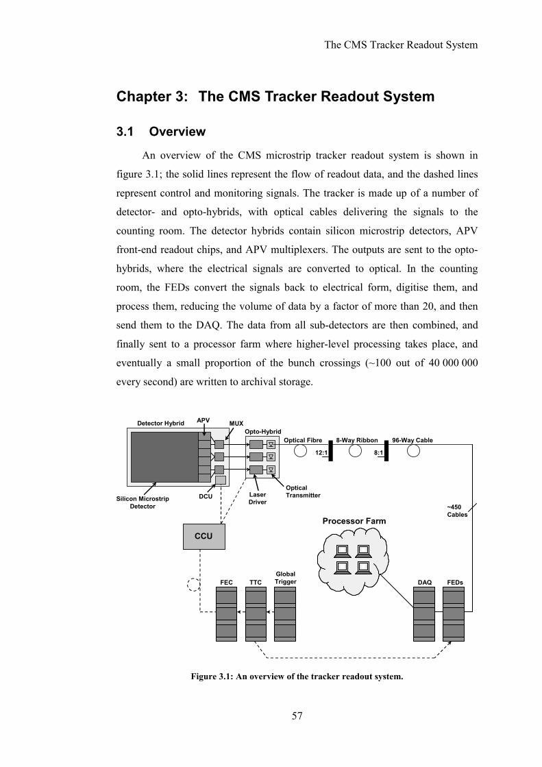
The CMS Tracker Readout System
57
Chapter 3: The CMS Tracker Readout System
3.1 Overview
An overview of the CMS microstrip tracker readout system is shown in
figure 3.1; the solid lines represent the flow of readout data, and the dashed lines
represent control and monitoring signals. The tracker is made up of a number of
detector- and opto-hybrids, with optical cables delivering the signals to the
counting room. The detector hybrids contain silicon microstrip detectors, APV
front-end readout chips, and APV multiplexers. The outputs are sent to the opto-
hybrids, where the electrical signals are converted to optical. In the counting
room, the FEDs convert the signals back to electrical form, digitise them, and
process them, reducing the volume of data by a factor of more than 20, and then
send them to the DAQ. The data from all sub-detectors are then combined, and
finally sent to a processor farm where higher-level processing takes place, and
eventually a small proportion of the bunch crossings (~100 out of 40 000 000
every second) are written to archival storage.
12:1 8:1
Optical Fibre 8-Way Ribbon 96-Way Cable
APV MUX
Silicon MicrostripDetector
Detector Hybrid
OpticalTransmitter
Processor Farm
FEDsDAQ
LaserDriver
Opto-Hybrid
CCUCCU
DCU
FEC TTCGlobalTrigger
~450Cables
Figure 3.1: An overview of the tracker readout system.
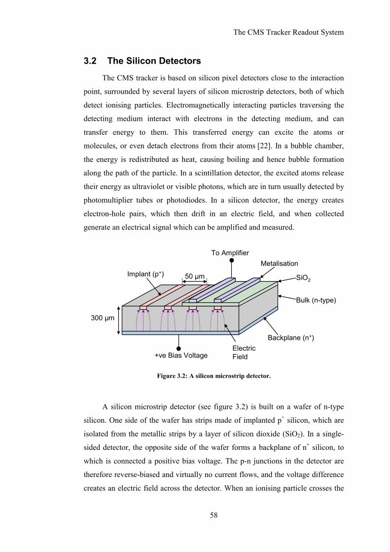
The CMS Tracker Readout System
58
3.2 The Silicon Detectors
The CMS tracker is based on silicon pixel detectors close to the interaction
point, surrounded by several layers of silicon microstrip detectors, both of which
detect ionising particles. Electromagnetically interacting particles traversing the
detecting medium interact with electrons in the detecting medium, and can
transfer energy to them. This transferred energy can excite the atoms or
molecules, or even detach electrons from their atoms [22]. In a bubble chamber,
the energy is redistributed as heat, causing boiling and hence bubble formation
along the path of the particle. In a scintillation detector, the excited atoms release
their energy as ultraviolet or visible photons, which are in turn usually detected by
photomultiplier tubes or photodiodes. In a silicon detector, the energy creates
electron-hole pairs, which then drift in an electric field, and when collected
generate an electrical signal which can be amplified and measured.
A silicon microstrip detector (see figure 3.2) is built on a wafer of n-type
silicon. One side of the wafer has strips made of implanted p+ silicon, which are
isolated from the metallic strips by a layer of silicon dioxide (SiO2). In a single-
sided detector, the opposite side of the wafer forms a backplane of n+ silicon, to
which is connected a positive bias voltage. The p-n junctions in the detector are
therefore reverse-biased and virtually no current flows, and the voltage difference
creates an electric field across the detector. When an ionising particle crosses the
Bulk (n-type)
Implant (p+)
Backplane (n+)
SiO2
Metalisation
+ve Bias VoltageElectricField
To Amplifier
300 µm
50 µm
Figure 3.2: A silicon microstrip detector.

The CMS Tracker Readout System
59
detector, the deposited energy generates electron-hole pairs. These drift in
opposite directions because of the electric field, the electrons towards the
positively charged backplane, and the holes toward the nearest strip. When the
holes reach a strip, a pulse of current is generated, which can be amplified and
measured by the readout electronics.
The energy deposited in the detector by a charged particle is described by
the Bethe-Bloch equation. It is approximately proportional to the electron density
in the detecting medium and to the square of the charge of the projectile particle.
It also depends on the energy of the particle; at low energy decreasing rapidly to a
minimum around βγ = 3-4, then rising logarithmically with higher energies, and
finally levelling off at a constant value. A particle near the minimum is known as
a minimum ionising particle (MIP). In a 300 µm silicon detector, this corresponds
to a charge deposition of about 25 000 electrons.
3.3 The APV Readout Chip
The APV readout chip (see figure 3.3) processes and buffers the signals
from the detectors. The chip reads out 128 strips of the microstrip detectors in
parallel, amplifying and shaping the pulses, then storing them in an analogue
pipeline. When ready, the signals are read out, further processed, and then
multiplexed out.
As it is located inside the detector, it must be able to withstand the huge
radiation levels that are present. Particle fluxes in the tracker are expected to be
about 1014 cm-2yr-1 and the total radiation dose over the lifetime of the experiment
up to 10 Mrad.
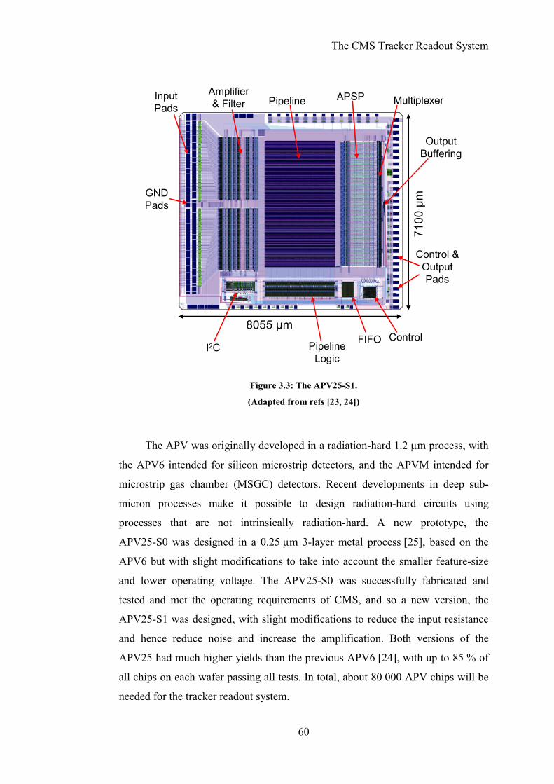
The CMS Tracker Readout System
60
The APV was originally developed in a radiation-hard 1.2 µm process, with
the APV6 intended for silicon microstrip detectors, and the APVM intended for
microstrip gas chamber (MSGC) detectors. Recent developments in deep sub-
micron processes make it possible to design radiation-hard circuits using
processes that are not intrinsically radiation-hard. A new prototype, the
APV25-S0 was designed in a 0.25 µm 3-layer metal process [25], based on the
APV6 but with slight modifications to take into account the smaller feature-size
and lower operating voltage. The APV25-S0 was successfully fabricated and
tested and met the operating requirements of CMS, and so a new version, the
APV25-S1 was designed, with slight modifications to reduce the input resistance
and hence reduce noise and increase the amplification. Both versions of the
APV25 had much higher yields than the previous APV6 [24], with up to 85 % of
all chips on each wafer passing all tests. In total, about 80 000 APV chips will be
needed for the tracker readout system.
8055 µm
7100
µm
Amplifier& Filter Pipeline APSP MultiplexerInput
Pads
I2C
Control &OutputPads
PipelineLogic
GNDPads
FIFO Control
OutputBuffering
Figure 3.3: The APV25-S1.
(Adapted from refs [23, 24])
The CMS Tracker Readout System
61
3.3.1 Preamplifier
The first stage in the APV is the preamplifier. It reads the signals and
amplifies them to a level of 18.7 mV per MIP (25 000 electrons). A switchable
unity-gain inverter allows the signal to be inverted if detectors of the opposite
polarity are used.
3.3.2 Shaping Filter
The output of the preamplifier is shaped by a CR-RC filter into a 50 ns wide
voltage pulse and further amplified. The combined amplification of the
preamplifier and filtering stages produce a pulse height of 100 mV per MIP.
3.3.3 Pipeline and FIFO
The output of the filter circuit is sampled at a rate of 40 MHz, and stored in
an analogue pipeline for the 3.2 µs latency until a level 1 trigger decision is made.
The pipeline is made up of 128 channels by 192 columns of switched capacitor
elements. The capacitors are made using the gates of 7 µm x 7 µm nFETs, which
have a capacitance of 0.28 pF. One side of the capacitor is connected to VSS, and
the other end to both the output of the shaper via a write switch, and the input of
the APSP via a read switch [26].
A write pointer circulates the pipeline, sampling the output of the shaper
every 25 ns. A trigger pointer follows it, separated by the trigger latency. When a
trigger is received, one or three columns, depending on the mode, are marked and
reserved for reading out. These will not be overwritten by any triggers until they
have been read out; the pointers instead skip over them to the next empty column.
A FIFO of depth 32 stores the column addresses of the marked data in the
pipeline, so that they are read out in the right order.
3.3.4 APSP
The APV has two main modes of operation, peak mode and deconvolution
mode. In peak mode, one sample is reserved in the pipeline for each trigger
received, corresponding to the peak of the CR-RC shaped pulse. This maximises
the signal-to-noise ratio and minimises the non-linearity of the system, and is used
when the data occupancy in the tracker is expected to be relatively low. When
The CMS Tracker Readout System
62
occupancy is higher, the incoming pulses get closer together, and can start getting
superimposed on one another. This is known as pile-up, and if it becomes
significant, then the APV can be run in deconvolution mode. In this case, three
samples are stored in the pipeline for every trigger, and these are then
deconvoluted by the Analogue Pulse Shape Processor (APSP).
The APSP is a three-weight Finite Impulse Response (FIR) filter, consisting
of a charge amplifier and a switched capacitor network. The filter performs a
deconvolution of the input data by producing a weighted sum of the three inputs
(corresponding to three samples of the input signal at different times). This
technique can be easily implemented in CMOS technology, and has low power
consumption [27].
The operation of the APSP is shown in figure 3.4. The three pipeline
columns are sampled into three capacitors, one after the other, by ri1 , ri2 ,
and ri3 . The feedback capacitor is then increased by last_cycle, the charges on
the three capacitors summed by ro1, ro2, and ro3, and the resulting signal stored
on the hold capacitor by store . The DC output level can be adjusted by the
signal Vadj. The effect of the filter is to reduce the width of the output pulse to fit
within one 25 ns bunch-crossing period.
The chip actually has a third mode of operation, called multi mode, where
three consecutive samples are made on each trigger (as in deconvolution mode),
but all three are output as consecutive frames by the multiplexer, each processed
by the APSP as in peak mode. This is useful when calibrating the timing, as
consecutive triggers to the APV must be separated by at least two clock cycles, so
this mode allows a run of frames from consecutive clock cycles to be read out.

The CMS Tracker Readout System
63
3.3.5 Analogue Multiplexer
The outputs from the 128 channels of the APSP are read out by a 128-
channel analogue multiplexer and driven off the chip as a differential current. Due
to the way the multiplexer is implemented, in three levels, the order in which the
data are transmitted does not correspond to the physical order in the detector; but
this reordering can be easily undone at a later stage in the readout chain. The
outputs of the APSP are converted to a current by a resistor, which has five
programmable values, allowing the gain of the multiplexer to be trimmed. The
output of the multiplexer is a current of magnitude 100 µA per MIP. This is then
converted to a differential signal, linearised, and amplified by a factor of 10,
generating an output current of ±1 mA per MIP.
11
22
33
11 22 33
44
44
Figure 3.4: The APV25 APSP circuit.
(Adapted from ref [26])
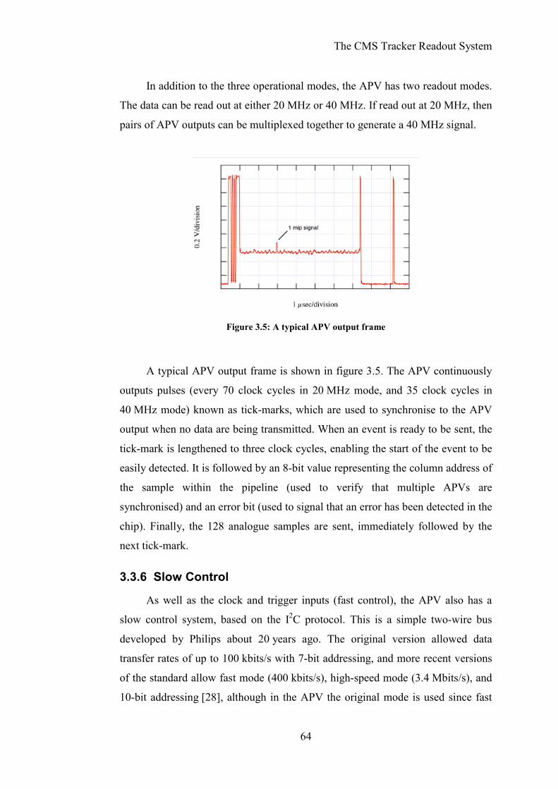
The CMS Tracker Readout System
64
In addition to the three operational modes, the APV has two readout modes.
The data can be read out at either 20 MHz or 40 MHz. If read out at 20 MHz, then
pairs of APV outputs can be multiplexed together to generate a 40 MHz signal.
A typical APV output frame is shown in figure 3.5. The APV continuously
outputs pulses (every 70 clock cycles in 20 MHz mode, and 35 clock cycles in
40 MHz mode) known as tick-marks, which are used to synchronise to the APV
output when no data are being transmitted. When an event is ready to be sent, the
tick-mark is lengthened to three clock cycles, enabling the start of the event to be
easily detected. It is followed by an 8-bit value representing the column address of
the sample within the pipeline (used to verify that multiple APVs are
synchronised) and an error bit (used to signal that an error has been detected in the
chip). Finally, the 128 analogue samples are sent, immediately followed by the
next tick-mark.
3.3.6 Slow Control
As well as the clock and trigger inputs (fast control), the APV also has a
slow control system, based on the I2C protocol. This is a simple two-wire bus
developed by Philips about 20 years ago. The original version allowed data
transfer rates of up to 100 kbits/s with 7-bit addressing, and more recent versions
of the standard allow fast mode (400 kbits/s), high-speed mode (3.4 Mbits/s), and
10-bit addressing [28], although in the APV the original mode is used since fast
Figure 3.5: A typical APV output frame

The CMS Tracker Readout System
65
data rates are not needed. The APV has a number of internal registers, which
control internal voltage and current biases, set the mode of operation and the
programmable latency, and hold error flags. These can be written and read back
via the I2C bus.
3.4 The APVMUX
The outputs from pairs of APVs (each driven at 20 MHz) are multiplexed
together by APV multiplexer (APVMUX) chips, each of which contains two
2-to-1 multiplexers. The differential current output of the APV is converted to a
voltage by internal resistors connected to a reference voltage pad [29]. The value
of these resistors can be switched to a range of values between 50 and 200 Ω by a
register controlled by an I2C connection.
3.5 The Optical Link
The output of the APVMUX is sent to the optical hybrid, where the
electrical signals are converted into optical signals. Each opto-hybrid contains
either two or three (depending on its geometrical position in the detector) laser
drivers and laser diodes [30]. The laser drivers bias the laser diodes at their
working point, and modulate them with a signal proportional to the input signal.
The laser diodes convert the signals from electrical to optical, and transmit them
in analogue form over optical fibres. At patch-panels inside the detector, groups of
12 fibres are bundled together in ribbons, and then 8 ribbons are grouped together
into cables. These then take the signals out to the counting room where they are
processed further.
The CMS Tracker Readout System
66
3.6 The Front-End Driver
The front-end drivers (FEDs) are located in the counting room, and receive
the analogue optical signals from the front-end of the detector. The tracker has a
total of about 440 FEDs, located in 24 crates, in 8 racks (see figure 3.6). Each
crate holds 18 FEDs, along with a crate controller with a 100 Mbps Ethernet
connection, and two spare slots for possible other cards. The 440 FEDs work in
parallel to process data from all 10 million channels in the tracker. This involves
converting the optical signals into electrical form, amplifying and digitising them,
then subtracting unwanted components of the signal and performing cluster
finding and zero suppression to reduce the volume of data sent to the DAQ. The
internal operation of the FED is described in more detail in the next chapter.
DAQFED
LAN
1 212
FE 1
DAQ
TTC
FE 2
FE 3
FE 4
FE 5
FE 6
FE 7
100MBit/s
B-ScanF-BusNN Synch
100 KHz
FE 8
Throttle
Figure 3.6: The FED and DAQ racks (top) and a FED crate (bottom).
(Adapted from ref [31])

The CMS Tracker Readout System
67
3.7 The S-LINK64
The data produced by the FED are transmitted to the DAQ over a fast data
link known as S-LINK64, which is an extension of the S-LINK specification. S-
LINK is a simple link interface that can be used to connect a layer of the front-end
electronics to the next level of readout. In addition to transferring data, it provides
error detection, and optional return signals providing two-way communication.
The physical medium of the link is not specified by the standard, and could be
implemented as an optical fibre, copper wires, or any other medium that meets the
required transmission speeds. Since the FED crates will be close to the DAQ
system, in this case it is likely to use copper wires; for distances in excess of about
15 meters [32] it would be necessary to use optical fibres. With S-LINK, data can
be 8, 16 or 32-bits wide, and can be transmitted up to a maximum clock frequency
of 40 MHz [33]. The S-LINK64 standard extends this to 64 bits, and up to a
maximum clock frequency of 100 MHz [34], corresponding to 800 Mbyte/s.
3.8 The DAQ
An overview of the DAQ architecture is shown in figure 3.7. It receives the
signals from the FEDs of the various subdetectors via the S-LINK64 fast copper
links. The builder network is a large switching fabric, providing interconnections
between the FED readout systems and the filter systems, and is capable of
sustaining a data transfer rate of 800 Gbyte/s [35]. For each event, the fragments
from the different subdetectors are combined, and sent to one of the filter systems.
Figure 3.7: Overview of the CMS DAQ system.
(From ref [35])
The CMS Tracker Readout System
68
The filter systems consist of a network of processors that verify the
integrity of the received data, and execute the high-level trigger algorithms that
select the events to be stored for offline analysis. These are then sent to the
computing services, where they are forwarded to mass storage. The computing
services also perform monitoring of the high-level trigger system and of the
detector itself.
3.9 Control and Monitoring
As well as reading out and processing data from the tracker, it is necessary
to distribute signals, such as clock, level-1 accept and reset commands, to all the
readout electronics and to monitor their state (e.g. temperature) to ensure that
everything is working properly.
3.9.1 Timing, Trigger and Control (TTC)
The TTC information is broadcast to the detector over optical fibres, using
Time Division Multiplexing (TDM) and BiPhase Mark (BPM) encoding to
encode two channels (A and B) onto a single fibre [36]. Channel A is dedicated to
transmitting the level 1 accept decisions, a one-bit decision being transmitted on
every bunch crossing. Channel B transmits the trigger number reset and bunch
counter reset commands, as well as individually addressed commands and data,
which transmit user-defined information over the network, and allow the TTC
receivers to be controlled centrally. The 40.08 MHz LHC clock is not explicitly
encoded, but due to the regular transitions at well defined times in the BPM-
encoded signal, it can be easily recovered.
The TTC signals are received and decoded by the TTCrx chip, which is a
custom ASIC developed at CERN. It contains a number of registers controlled by
the incoming TTC signals, and also accessible via an I2C interface. The bunch
counter register is a free-running 12-bit counter incremented by the 40.08 MHz
clock, and the 24-bit event number counter is incremented by the level 1 accept
signal. Both counters can be reset by commands sent over the TTC system.
The CMS Tracker Readout System
69
3.9.2 The Tracker Control System (TCS)
An overview of the TCS is shown in figure 3.8. It consists of Front-End
Controllers (FECs) in the control room, connected to CCU modules in the tracker
by digital optical fibres. Groups of CCU modules are connected in loops, with two
connections. One of them links all of the modules in a continuous loop, and the
other connects alternative modules, allowing a closed loop to be sustained in the
case of failure of one of the modules.
CCU modules communicate with components on the detector and opto-
hybrids, such as the APVs, APVMUX, laser driver, and the DCU modules. The
DCU modules perform generic monitoring of variables such as temperature,
voltage, and current, using a 12-bit ADC.
This system allows the overall state of the tracker to be continuously
monitored, to ensure the proper functioning of the detector.
3.10 Summary
The tracker readout system samples 10 million silicon detector channels at
the LHC bunch-crossing rate of 40 MHz. The data are stored in the APV readout
chips, in the detector, until an L1A trigger decision has been made. The signals
are then sent over optical fibres to the counting room, where they are processed by
an array of 440 FEDs. The volume of data is reduced by a factor of 20 using zero-
suppression, and the results sent over a fast link to the DAQ. Here they are further
processed, and a small proportion of the events are written to archival storage.
Figure 3.8: Schematic of the tracker control system.
70
Chapter 4: The Front-End Driver The FED design is based on a VME64x 9U x 400 mm card. It receives the
analogue optical signals from the tracker, digitises and processes them, and then
transmits the resulting data to the CMS DAQ using S-LINK64 fast copper links.
The S-LINK64 transmitter (a PCI Mezzanine card) is plugged onto a transition
card, which is in turn plugged onto the back of the FED. In this way it is not
necessary to bring the S-LINK cable out through the front-panel of the FED,
which is already highly populated.
Each FED (see figure 4.1) has eight identical sections at the front of the
PCB known as front-end modules, each of which processes data from twelve
channels (one ribbon, corresponding to 24 APVs) via an optical connector on the
front-panel. Each module contains six dual-ADCs, three delay FPGAs to tune the
timing of the individual channels, and a front-end FPGA, which processes the
data. The data produced by the front-end modules are combined and buffered by
the back-end FPGA prior to being sent to the DAQ system via a transition card
DAQFRL
DAQ MezzanineCard
Transition Card
BusyThrottle
S-LINK64TTCrx
BE FPGA
Buffers
1212
1212
1212
1212
1212
1212
1212
1212
TTC
TCS
VME FPGA
FPGAConfig:
SystemACE CF
Hot SwapPowerDC-DC
96 TrackerOpto Fibres
VMEInterface
TempMonitor
JTAG
Front-End Modules x 8Double-sided board
XilinxVirtex-IIFPGA
9U VME64x Card
Warning
Opto-RXFE FPGA
Delay FPGA
Analogue/ADC
Figure 4.1: Schematic of the Front-end driver.
(Adapted from ref [31])
The Front-End Driver
71
which plugs onto the back of the FED. The back-end FPGA also receives TTC
information such as the clock, L1A and reset signals, via a separate optical
connection on the front-panel. A separate FPGA, which is configured separately
from the others via its own PROM, provides the connection to the VME bus. In
this way, the other FPGAs can be reconfigured via VME without risk of losing the
VME connection if a bad configuration is loaded.
All FPGAs on the board are from the Xilinx Virtex-II range, with speed
grade –4 and fine-pitch ball grid array packages. The 24 delay FPGAs are
XC2V40 parts with 144-pin packages, the 8 front-end FPGAs and the back-end
FPGA are XC2V2000 parts with 676-pin packages, and the VME FPGA is a
XC2V1000 part with a 456-pin package.
4.1 The FED Front-End Modules
Each front-end module processes twelve channels in parallel. It contains a
photodiode array, six high-bandwidth dual-ADCs, three delay FPGAs and a front-
end FPGA (see figure 4.2). The optical ribbon is connected to an opto-receiver
package consisting of 12 p-i-n photodiodes and an amplifier, producing twelve
single-ended current outputs [37].
12 FibreRibbon
PD A
rray
111
2
1
23
4
35
6
2
47
8
59
10
3
611
12
5*
CLK
DCM
CLK40 from TTC
Opto Rx
6
CLOCK
CONTROLDATA
DATA OUT@ 160 MHz
3 N
FullPartially Full
RESET
Front-EndFPGA
DelayFPGA
Dual ADC10-bits40 MHz
OpAmp
XC2V1500XC2V40AD9218EL2140
CLK
CLK
10ASIC
4*
DataControl
12x DACTempSensorLM82
* Double Data Rate I/O
Figure 4.2: Schematic of a FED front-end module.
(Adapted from ref [31])
The Front-End Driver
72
These are converted into double-ended voltage signals for the ADC by the
circuit shown in figure 4.3. The input arrives at the pin labelled OPTOA; a load
resistor converts the current to a voltage, which is then connected to the non-
inverting input of the op-amp. The inverting input is connected to a reference
voltage, which can be set individually for each channel by a 12-way DAC in order
to match each channel to the ADC input range. The op-amp generates a
differential voltage signal on the pins AINA_T and AINABAR_T.
These signals are then digitised by commercial 40 MHz 10-bit dual-ADCs
(see figure 4.4). The two differential input signals arrive on the pins
AINA_T/AINABAR_T and AINB_T/AINBBAR_T, and the ADC generates two 10-
bit digital signals on the pins TOP_DA(0-9) and TOP_DB(0-9). The other
connections to the ADC consist of the power supply and clock signals.
Figure 4.3: Schematic of a FED front-end module analogue section.
(From ref [38])
The Front-End Driver
73
Figure 4.4: Schematic of a FED front-end module two channel ADC.
(From ref [38])
The Front-End Driver
74
The individual fibres connected to the FED are unlikely to be all exactly of
the same length, and therefore the signals will all arrive at slightly different times.
To compensate for this, each ADC has a separate clock input (generated by the
delay FPGAs, and controlled by the front-end FPGAs) that can be individually
skewed relative to the main clock, allowing the sampling point to be controlled at
the level of 1/32 of a clock cycle, or 781 ps [39]. The outputs of the ADCs are then
sampled, using the main clock, by the delay FPGA, bringing them all into the
main clock domain. In addition, the delay FPGA contains a variable length
pipeline, allowing the data to be delayed by up to 16 clock cycles. The values of
the clock skew settings will be calculated by software, outside of the FED, and
stored in a database to be loaded during the setting up of the FEDs.
By looking for the regular tick-marks sent by the APVs, the FED is able to
adjust the timing automatically, so that the signals from all fibres arrive at the
same time to within the level of about 1/32 of a clock cycle (781 ps) [40]. This can
be done by scanning over a 70-clock cycle range (the distance between two tick
marks), in 781 ps steps, and looking for the rising edge of the tick-mark.
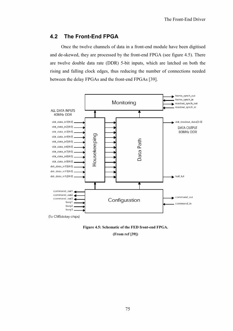
The Front-End Driver
75
4.2 The Front-End FPGA
Once the twelve channels of data in a front-end module have been digitised
and de-skewed, they are processed by the front-end FPGA (see figure 4.5). There
are twelve double data rate (DDR) 5-bit inputs, which are latched on both the
rising and falling clock edges, thus reducing the number of connections needed
between the delay FPGAs and the front-end FPGAs [39].
Figure 4.5: Schematic of the FED front-end FPGA.
(From ref [39])
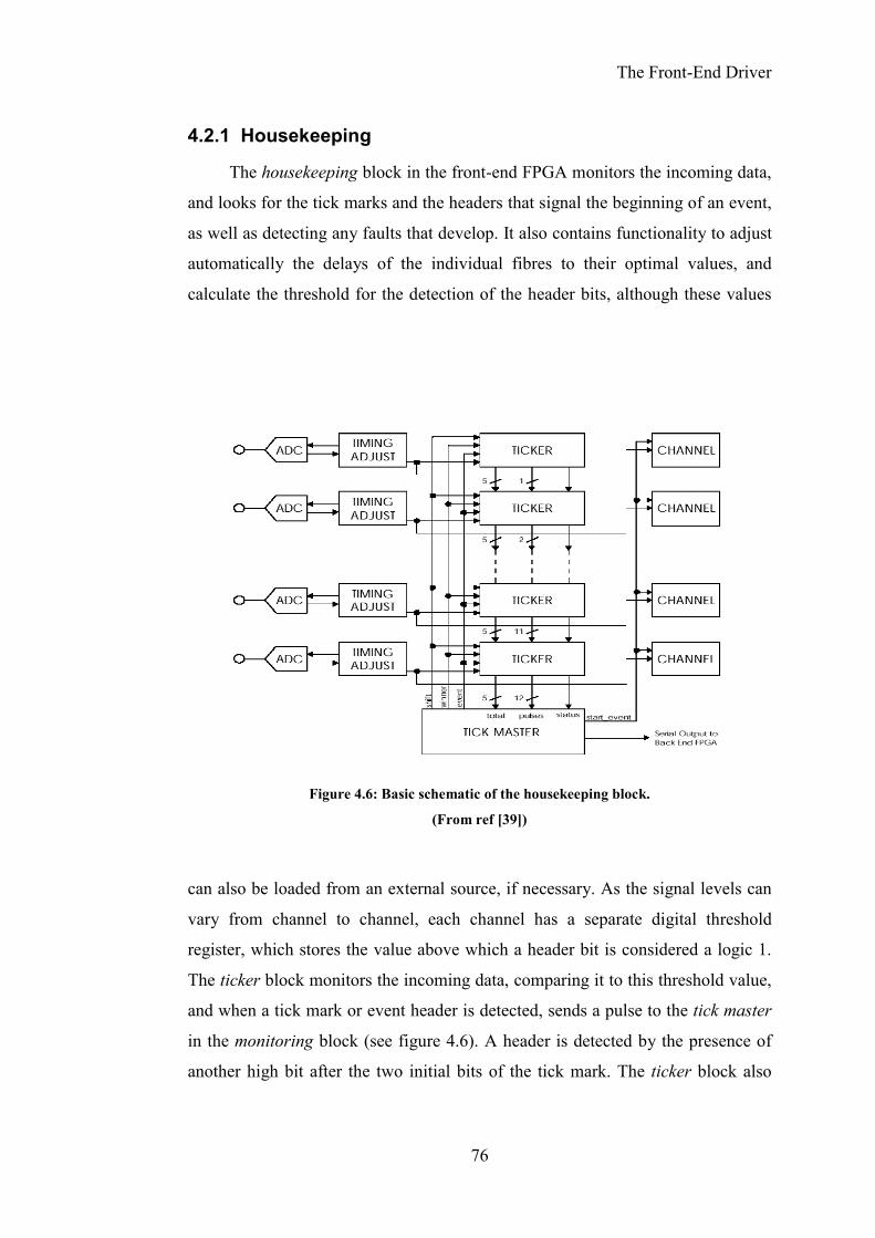
The Front-End Driver
76
4.2.1 Housekeeping
The housekeeping block in the front-end FPGA monitors the incoming data,
and looks for the tick marks and the headers that signal the beginning of an event,
as well as detecting any faults that develop. It also contains functionality to adjust
automatically the delays of the individual fibres to their optimal values, and
calculate the threshold for the detection of the header bits, although these values
can also be loaded from an external source, if necessary. As the signal levels can
vary from channel to channel, each channel has a separate digital threshold
register, which stores the value above which a header bit is considered a logic 1.
The ticker block monitors the incoming data, comparing it to this threshold value,
and when a tick mark or event header is detected, sends a pulse to the tick master
in the monitoring block (see figure 4.6). A header is detected by the presence of
another high bit after the two initial bits of the tick mark. The ticker block also
Figure 4.6: Basic schematic of the housekeeping block.
(From ref [39])

The Front-End Driver
77
checks that a tick mark is received every 70 clock cycles (except during a data
frame), hence verifying that the FED remains in synchronisation.
4.2.2 Monitoring
The tick master monitors the signals from the tickers. If a clear majority
(more than 50%) of channels detect a frame on the same clock cycle, an event-
start signal is sent to all channels, and any that did not trigger can set their status
bits accordingly. Once a frame has been recognised, the digital header has to be
extracted. If all is well, then all 12 headers should be identical, but it is possible
that some APVs may be out of synchronisation and therefore be sending the
wrong headers. In this case the header is calculated as the bit-by-bit majority
value of all the received headers, i.e. for each bit, the majority (1 or 0) is
calculated, independent of the other bits. As long as the majority of APVs remain
in synchronisation, then this will always be the correct value. The number of
APVs out of synchronisation is transmitted with the data, so if too many APVs
lose synchronisation a reset signal can be sent. The monitoring block then sends a
frame_synch_out signal to the back-end FPGA with the majority header, and the
status bits for each channel. The status bits indicate whether the channel has
locked on to a signal (i.e. it is detecting tick-marks at the expected time every 70
clock-cycles), whether it is in synchronisation with the other channels, whether
either APV sent the wrong header (compared to the majority header), and whether
either APV had the error bit set in its header.
The monitoring block also checks regularly the state of the datapath block.
Once a frame has been processed by the data path and stored in the front-end
buffer, a second signal, readout_synch_out, containing a 14-bit number with the
length of the zero-suppressed event in the buffer, is sent to the back-end FPGA. In
the normal zero-suppression mode this will always occur 559 clock cycles (at
40 MHz) after the first bit of the frame_synch_out signal.
4.2.3 Configuration
The configuration block controls the loading and reading back of all the
various parameters of the front-end modules. These include the delay and digital
threshold values for each fibre, the enable/disable bits for each APV, the pedestal

The Front-End Driver
78
data, and the mode of operation. It can also set the control bits for the opto-
receivers, the ADCs, and the reference-voltage DACs, as well as passing control
signals back to the delay FPGAs.
4.2.4 Data Path
The main processing takes place in the front-end FPGA data path block.
This contains twelve almost-identical channels (some of the memory blocks are
shared between pairs of channels), each processing data from one pair of APVs.
Each channel contains a number of blocks, which subtract unwanted
components of the signal, find clusters of hits, and buffer the data. The raw signal
can be decomposed into several different components in addition to the useful
data, namely the pedestal, common-mode, and random noise. The pedestal is the
component of the signal that is constant from event to event, but is different for
each strip. It can be calculated by averaging the data from the APVs in the
absence of any hits, and the result can then be stored in a look-up table for later
use. The common-mode is a DC level that varies from event to event, but is
assumed to be constant for the duration of a single event. It is estimated by
averaging all of the strips except those containing hits. If hits are present in the
10 11
trig2
Ped-
Sub
11
trig3
Re-
Ord
erC
M-S
ub 8
Hit-
Find
ing
s-datas-addr8
16
hit
Pack
etis
er
4
averages 8header control
DPM
16
No hits
Sequ
ence
r-M
ux
8 8a
d
a
d
10
trig1
11
trig2
Ped-
Sub
11
trig3
Re-
Ord
erC
M-S
ub 8
Hit-
Find
ing
s-datas-addr8
16
256 cycles 256 cycles
hit DPM
16
No hits
Sequ
ence
r-M
ux
8 8a
d
a
d
status
averages 8header status
nx256x16
trig4
Mux
data
2 x 256 cycles 256 cycles nx256x16
trig1
160 MHz
data
data
Monitoring
Figure 4.7: A pair of channels from the datapath block.
(Adapted from ref [39])
The Front-End Driver
79
data, this requires at least two passes, first to calculate an average, then to exclude
strips significantly higher than this average and calculate a better estimate
ignoring these strips. It turns out to be better to calculate the median of all the
strips, which still needs two passes over the data, but is less prone to bias from the
hits. The random noise component varies from strip to strip and from frame to
frame, and is therefore impossible to remove.
A pair of channels from the datapath block is shown in see figure 4.7; the
individual blocks are described below.
Ped-Sub
The first block receives the raw data from the ADC. It contains a look-up
table with the 256 pedestal values for the two APVs. The pedestal values are
subtracted from the raw data, and this is then sent to the next block for further
processing.
Re-order / CM-Sub
The second block performs the common-mode subtraction and reorders the
data. The common mode is calculated using a two-pass median technique, where
the first pass histograms the most significant five bits, and the second pass
histograms the least significant five bits. As the data arrive, they are written into
the re-ordering RAM and stored there while the median calculation takes place.
Once the median is ready, the data are read out of the reordering RAM in a
different order, so that the re-ordering of the APV multiplexer is undone, and at
the same time, the common mode is subtracted.
Hit-Finding
The reordered data are then searched for hits above threshold, which are
grouped into clusters. The FED uses one threshold for groups of more than one
contiguous strip, and a higher threshold for single strips, as these are more likely
to be caused by noise in the signal. The clustering block outputs the starting
address and length of each cluster, followed by the data for each strip in the
cluster, meaning that two words have to be output before each cluster. One word
is sent per clock cycle, so there must be two empty clock cycles before each

The Front-End Driver
80
cluster. To ensure that this is always the case, clusters that are only separated by a
single strip are merged together into a single cluster, including the intervening
strip. The algorithm is shown graphically in figure 4.8. The data flows from top to
bottom along the left-hand side, and word n represents the current strip, which is
examined along with the neighbouring two strips on each side. Each strip is
compared to the two thresholds, and the results of these comparisons are then
masked by different patterns. There are a number of pattern masks, representing
the different conditions for which any particular strip should be included in a
cluster. A 1 in the pattern means that the corresponding strip must be above the
multi-strip threshold, a 2 means that the strip must be above the single-strip
threshold, and an x means don’t care. The first two patterns check whether the
strip is part of a multi-strip cluster, the third checks whether it is a single-strip
cluster, and the remaining four patterns check if the strip is in the middle of two
clusters.
If none of the patterns are matched, then the corresponding strip is
discarded, as it contains no useful data. This is known as zero-suppression; it
significantly reduces the volume of the data, as only a minority of the strips
contain hits.
Figure 4.8: Graphical representation of the clustering algorithm.
(From ref [39])
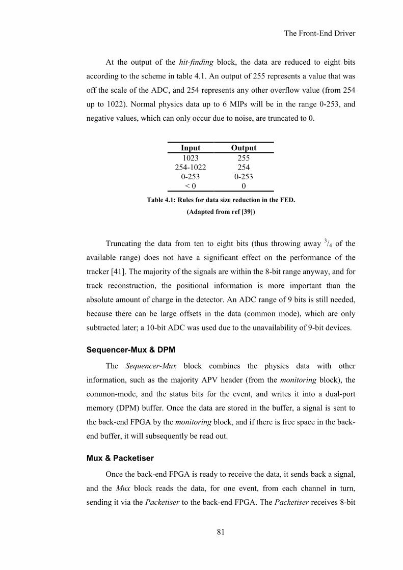
The Front-End Driver
81
At the output of the hit-finding block, the data are reduced to eight bits
according to the scheme in table 4.1. An output of 255 represents a value that was
off the scale of the ADC, and 254 represents any other overflow value (from 254
up to 1022). Normal physics data up to 6 MIPs will be in the range 0-253, and
negative values, which can only occur due to noise, are truncated to 0.
Truncating the data from ten to eight bits (thus throwing away 3/4 of the
available range) does not have a significant effect on the performance of the
tracker [41]. The majority of the signals are within the 8-bit range anyway, and for
track reconstruction, the positional information is more important than the
absolute amount of charge in the detector. An ADC range of 9 bits is still needed,
because there can be large offsets in the data (common mode), which are only
subtracted later; a 10-bit ADC was used due to the unavailability of 9-bit devices.
Sequencer-Mux & DPM
The Sequencer-Mux block combines the physics data with other
information, such as the majority APV header (from the monitoring block), the
common-mode, and the status bits for the event, and writes it into a dual-port
memory (DPM) buffer. Once the data are stored in the buffer, a signal is sent to
the back-end FPGA by the monitoring block, and if there is free space in the back-
end buffer, it will subsequently be read out.
Mux & Packetiser
Once the back-end FPGA is ready to receive the data, it sends back a signal,
and the Mux block reads the data, for one event, from each channel in turn,
sending it via the Packetiser to the back-end FPGA. The Packetiser receives 8-bit
Input Output 1023 255
254-1022 254 0-253 0-253
< 0 0
Table 4.1: Rules for data size reduction in the FED.
(Adapted from ref [39])
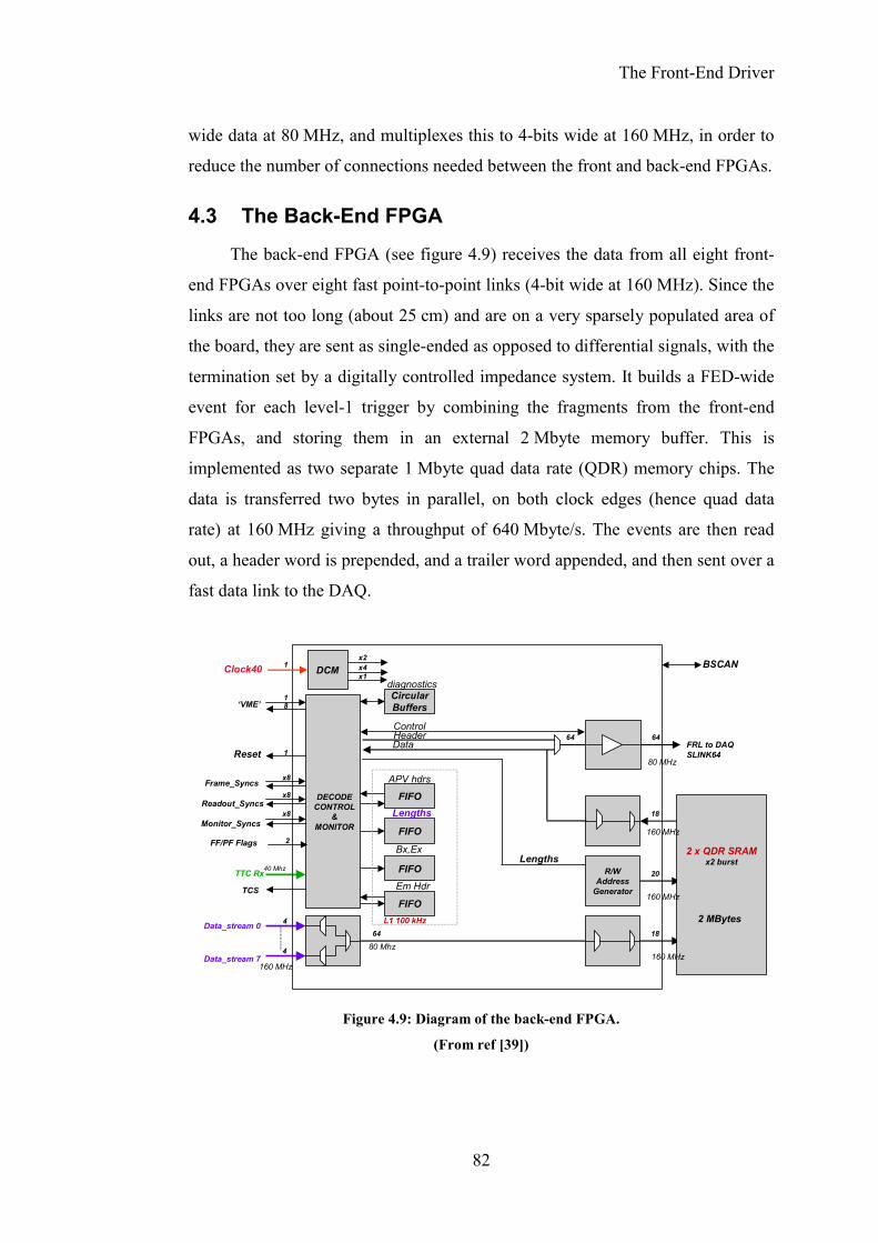
The Front-End Driver
82
wide data at 80 MHz, and multiplexes this to 4-bits wide at 160 MHz, in order to
reduce the number of connections needed between the front and back-end FPGAs.
4.3 The Back-End FPGA
The back-end FPGA (see figure 4.9) receives the data from all eight front-
end FPGAs over eight fast point-to-point links (4-bit wide at 160 MHz). Since the
links are not too long (about 25 cm) and are on a very sparsely populated area of
the board, they are sent as single-ended as opposed to differential signals, with the
termination set by a digitally controlled impedance system. It builds a FED-wide
event for each level-1 trigger by combining the fragments from the front-end
FPGAs, and storing them in an external 2 Mbyte memory buffer. This is
implemented as two separate 1 Mbyte quad data rate (QDR) memory chips. The
data is transferred two bytes in parallel, on both clock edges (hence quad data
rate) at 160 MHz giving a throughput of 640 Mbyte/s. The events are then read
out, a header word is prepended, and a trailer word appended, and then sent over a
fast data link to the DAQ.
FIFO
FIFO
FIFO
FIFO
CircularBuffers
Frame_Syncs
Readout_Syncs
Monitor_Syncs
x8
x8
x8
TTC Rx
TCS
‘VME’
DECODECONTROL
&MONITOR
Data_stream 0
Data_stream 7
64 18Data In
20Address
18 Data Out
64FRL to DAQSLINK64
64
R/WAddress
Generator
APV hdrs
Lengths
Bx,Ex
Em Hdr
diagnostics
Data
80 Mhz
L1 100 kHz4
4
160 MHz
40 Mhz
Clock40
Reset
DCMx1
x2x4
2 x QDR SRAMx2 burst
BSCAN
160 MHz
160 MHz
160 MHz
80 MHz
Lengths
Header
FF/PF Flags 2
8
1
1
1
Control
2 MBytes
Figure 4.9: Diagram of the back-end FPGA.
(From ref [39])
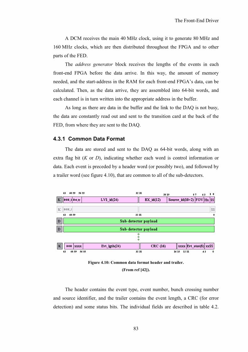
The Front-End Driver
83
A DCM receives the main 40 MHz clock, using it to generate 80 MHz and
160 MHz clocks, which are then distributed throughout the FPGA and to other
parts of the FED.
The address generator block receives the lengths of the events in each
front-end FPGA before the data arrive. In this way, the amount of memory
needed, and the start-address in the RAM for each front-end FPGA’s data, can be
calculated. Then, as the data arrive, they are assembled into 64-bit words, and
each channel is in turn written into the appropriate address in the buffer.
As long as there are data in the buffer and the link to the DAQ is not busy,
the data are constantly read out and sent to the transition card at the back of the
FED, from where they are sent to the DAQ.
4.3.1 Common Data Format
The data are stored and sent to the DAQ as 64-bit words, along with an
extra flag bit (K or D), indicating whether each word is control information or
data. Each event is preceded by a header word (or possibly two), and followed by
a trailer word (see figure 4.10), that are common to all of the sub-detectors.
The header contains the event type, event number, bunch crossing number
and source identifier, and the trailer contains the event length, a CRC (for error
detection) and some status bits. The individual fields are described in table 4.2.
Figure 4.10: Common data format header and trailer.
(From ref [42]).
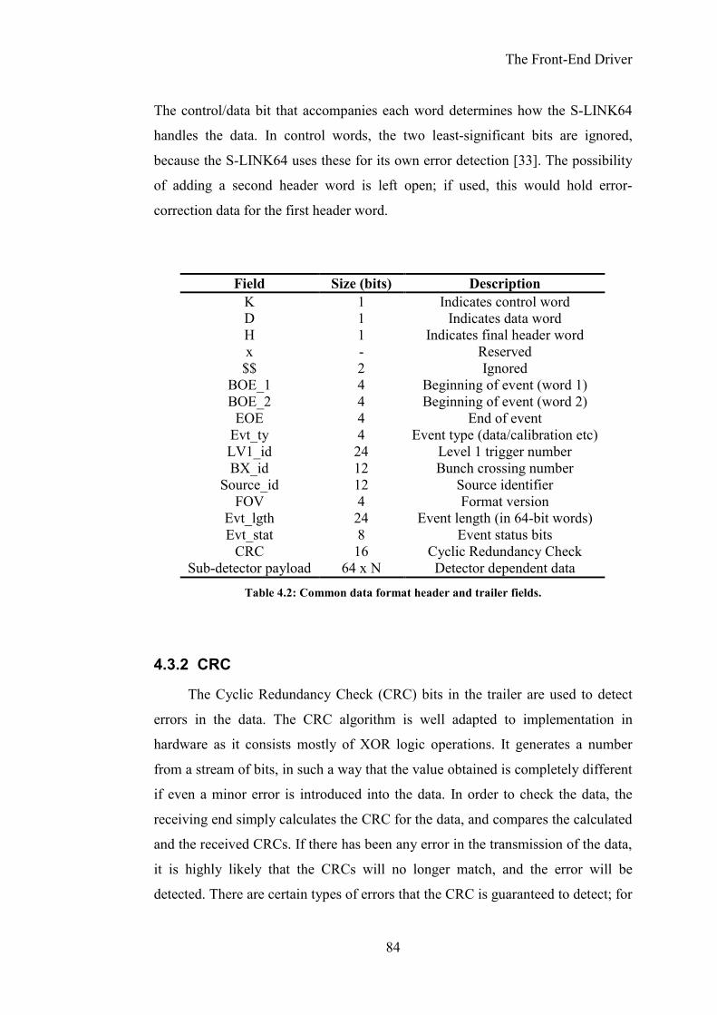
The Front-End Driver
84
The control/data bit that accompanies each word determines how the S-LINK64
handles the data. In control words, the two least-significant bits are ignored,
because the S-LINK64 uses these for its own error detection [33]. The possibility
of adding a second header word is left open; if used, this would hold error-
correction data for the first header word.
4.3.2 CRC
The Cyclic Redundancy Check (CRC) bits in the trailer are used to detect
errors in the data. The CRC algorithm is well adapted to implementation in
hardware as it consists mostly of XOR logic operations. It generates a number
from a stream of bits, in such a way that the value obtained is completely different
if even a minor error is introduced into the data. In order to check the data, the
receiving end simply calculates the CRC for the data, and compares the calculated
and the received CRCs. If there has been any error in the transmission of the data,
it is highly likely that the CRCs will no longer match, and the error will be
detected. There are certain types of errors that the CRC is guaranteed to detect; for
Field Size (bits) Description K 1 Indicates control word D 1 Indicates data word H 1 Indicates final header word x - Reserved $$ 2 Ignored
BOE_1 4 Beginning of event (word 1) BOE_2 4 Beginning of event (word 2)
EOE 4 End of event Evt_ty 4 Event type (data/calibration etc)LV1_id 24 Level 1 trigger number BX_id 12 Bunch crossing number
Source_id 12 Source identifier FOV 4 Format version
Evt_lgth 24 Event length (in 64-bit words) Evt_stat 8 Event status bits
CRC 16 Cyclic Redundancy Check Sub-detector payload 64 x N Detector dependent data
Table 4.2: Common data format header and trailer fields.

The Front-End Driver
85
other errors its effectiveness depends on its length, N. The probability of an error
going undetected is 2-N; for a 16-bit CRC this is 1 in 65536.
The CRC algorithm effectively treats the message as one huge binary
number, which it divides by another number and returns the remainder [43].
However, instead of using normal arithmetic, it uses what is known as polynomial
arithmetic modulo 2. This means that no carries are performed between adjacent
digits of the numbers, and each digit is only stored modulo 2 (i.e. can only be 0 or
1). It turns out that in this system addition and subtraction are the same, and are
both equivalent to the XOR logic operation. Therefore, as division is effectively
repeated subtraction, the algorithm becomes a series of XORs.
The number by which the data is divided is known as the polynomial of the
CRC. For any given length CRC, there are a number of possible polynomials,
with the highest term being the length of the polynomial. For example, the
standard 32-bit CRC (CRC-32) uses the polynomial 1 + x1 + x2 + x4 + x5 + x7 + x8
+ x10 + x11 + x12 + x16 + x22 + x23 + x26 + x32, often written as (0, 1, 2, 4, 5, 7, 8,
10, 11, 12, 16, 22, 23, 26, 32). A graphical representation of the algorithm is
shown in figure 4.11, for the polynomial (0, 1, 2, 8). As this is an 8-bit CRC, an 8-
bit register is used. The data is fed into this register one bit at a time, and the
register is shifted to the left. The bit that ‘falls off’ the left of the register is then
fed back in, by XORing it with several bits in the register. Which bits are affected
depends on the polynomial used, in this case bits 0, 1, and 2.
In practice, it is not necessary to process the data only one bit at a time.
Many implementations process 8 bits at a time, using a 256-location look-up
table, which stores the effect of any 8-bit sequence on the CRC. In hardware,
10010111101011…Bit stream
Poly = x8 + x2 + x + 1
1 0 1 1 0 0 1 01 1 0 1 1 0 0 1 01
7 6 5 4 3 2 1 08 7 6 5 4 3 2 1 08
Figure 4.11: Graphical representation of the CRC algorithm (for CRC-8).
The Front-End Driver
86
many logic operations can take place in parallel, and a look-up table is not needed
to create efficient implementations that process many bits at a time.
Some polynomials are better than others at detecting various types of errors.
For example, a CRC is guaranteed to detect all single-bit errors if the polynomial
has at least two bits set (i.e. two terms). If the polynomial has an even number of
bits set, then it will also catch all errors that modify an odd number of bits (in fact,
a parity bit is a trivial example of one such CRC, with length 1). Additionally, if
the lowest bit of the polynomial is set, then the CRC is guaranteed to detect all
burst errors with lengths up to that of the CRC. However, choosing a good
polynomial is extremely difficult and involves a large amount of complex
mathematics. In practice, there are a number of standard polynomials, already
proven and in widespread use, and it is usual to use one of these.
The initial value of the CRC, before any data are processed, can be chosen
arbitrarily. However, a value of zero will mean that any initial zeros in the data
stream would have no effect on the CRC, and therefore, any inserted zeros or
dropped bits in this region would go unnoticed. For this reason, a non-zero
starting value is often used.
An interesting characteristic of the CRC is that if the calculated CRC is
appended to the data, and the CRC is taken of this augmented data, the resulting
CRC will be zero. However, in most situations, it is just as easy to compare the
CRC of the data to the transmitted CRC, as it is to compare the CRC of the
augmented data to zero.
4.4 Implementation of Common Data Format
Code was developed in VHDL to implement this header format in the back-
end FPGA of the FED. The different blocks that make it up are shown in figure
4.12, and the VHDL code for each block is listed in appendix A. The main
processing, including the actual construction of the header and trailer words, takes
place in the builder block. It is notified when all the necessary information, such
as the trigger number and event length, is available for a new event by control
logic in the back-end FPGA, which sends a pulse to the prepare input. The header
and trailer are then assembled by the builder (apart from the CRC, which cannot
The Front-End Driver
87
be known before the event data are available), and sent to the FIFO block to be
stored until needed.
When the event data are ready to be read out, the control logic will notify
the builder block with a pulse on the start input. The builder then sends the header
word out to the MUX block, making a note of the length of the event. The control
logic can then start sending the data to the data_in input. With each word of data
sent, the CRC is updated, and the counter of the event length is decremented by
the builder block. When the entire event has been sent, the builder block sends the
trailer word, with the newly calculated CRC inserted in the appropriate place, to
the MUX block, which sends the resulting word to the output.

The Front-End Driver
88
data_in : (63:0) data_out : (63:0)
FED_DATA_FORMATmuxmux1
header_in : (63:0)
data_in_en
FED_DATA_FORMAT
addr_bits = fifo_addr_bits ( natural )
rd_enwr_en
data_evt_ty : (3:0)
data_lv1_id : (23:0)
data_bx_id : (11:0)
data_source_id : (11:0)
data_evt_stat : (7:0)
data_evt_lgth : (23:0)
Package ListLIBRARY ieee;USE ieee.std_logic_1164.ALL;
fifofifo1
clk
reset
clk
reset
empty
full
clk
reset
clk
reset
data_lv1_id : (23:0)
data_bx_id : (11:0)
data_evt_ty : (3:0)
G
G
wr_start
wr_data : (63:0)
clk
reset
wr_start
wr_
en
wr_
data
: (6
3:0)
wr_data : (63:0)
wr_en
reset
clk
data_in : (63:0)
data_evt_stat : (7:0)
data_source_id : (11:0)
data_evt_lgth : (23:0)
data_in_en
rd_start
rd_stop
clk
reset
rd_start
data_in_en
rd_stop
data_in : (63:0)
data_out : (63:0)
ctrl
data_out_en
header_sel : (1:0)
data_en
ctrl
linkfull
rd_data : (63:0)
rd_ready
wr_ready
FED_DATA_FORMATbuilderbuilder1
rd_d
ata
: (63
:0)
rd_e
n
wr_ready
data
_out
: (6
3:0)
data
_out
_sel
: (1
:0)
rd_ready
full
emp t
y
linkbusy
rd_data : (63:0)
rd_en
full
empty
Figure 4.12: Block diagram of the header formatting block.
The Front-End Driver
89
The mux block simply switches between the incoming data and the
header/trailer sent by the builder block. The header_sel input specifies whether
the mux should be outputting header, data, trailer or nothing. This allows the mux
to issue a warning during simulation if data is sent at the wrong time.
The fifo block buffers the header and trailer words until they are needed.
Internally it contains a 64-bit wide memory block (mem64) for storage, and it has
two pointers into this memory that define where data should be written, and from
where data should be read. Two outputs (full and empty) are also provided, which
allow detection of overflows and underflows during simulation.
The mem64 block (inside the fifo) provides a block of memory 64 bits wide,
and of variable depth, specified by a generic value. Three different
implementations were written, one using pairs of 32-bit wide Virtex II 16-kbit
block RAMs, one using Spartan II/Virtex 4-kbit block RAMs, and one general
implementation using an array of signals, which, when synthesised with Leonardo
Spectrum, uses distributed RAM.
The VHDL code for the actual CRC function (used in the builder block)
was generated with the Easics CRC Tool [44]. As the polynomial to be used in the
CRC of the trailer has not yet been decided, two different versions were
generated, corresponding to the two standard 16-bit CRC polynomials currently in
widespread use: the CCITT standard CRC-16, and the X.25 standard.
A testbench was written to verify the operation of the VHDL code. It sends
a range of typical signals to the header building block, using a pseudorandom
number generator to create the data for each event, and writes the output to a text
file. A short period of the simulation is shown in figure 4.13, following various
signals over a period of 1 µs. Each horizontal line represents a different signal,
with simulation time running from left to right. The top signal represents the
40 MHz system clock, followed by various other internal signals. The bottom
three signals represent the data_out_enable signal, the data/control bit and the 64-
bit wide data bus respectively, and the first event can be seen being transmitted
over these lines. A program was written in C to verify the output data, and both
the VHDL testbench and this C program are listed in appendix B.
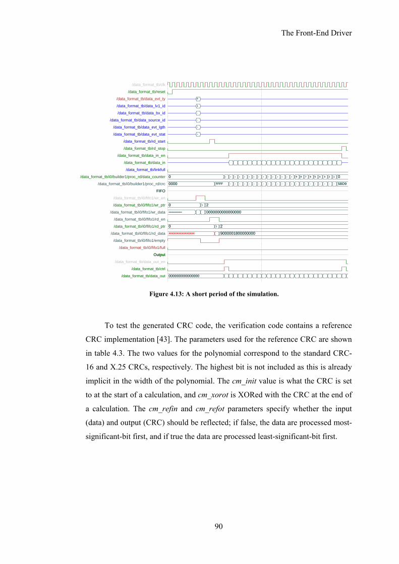
The Front-End Driver
90
To test the generated CRC code, the verification code contains a reference
CRC implementation [43]. The parameters used for the reference CRC are shown
in table 4.3. The two values for the polynomial correspond to the standard CRC-
16 and X.25 CRCs, respectively. The highest bit is not included as this is already
implicit in the width of the polynomial. The cm_init value is what the CRC is set
to at the start of a calculation, and cm_xorot is XORed with the CRC at the end of
a calculation. The cm_refin and cm_refot parameters specify whether the input
(data) and output (CRC) should be reflected; if false, the data are processed most-
significant-bit first, and if true the data are processed least-significant-bit first.
F
1
006
B38
24
00
0 24 23 22 21 20 19 18 17 16 15 14 13 12 11 10 9 8 7 6 5 4 3 2 1 0
0000 FFFF 80A4 BBCE 07AF 464E E19C E7BB C59D 11DA 6D58 35E1 6FC1 08DF 31C4 E545 C36F 569B D880 15C1 0A09 52D2 D2DC 15C5 7FFB 5BD9
FIFO
0 1 2
0000000000000000 0000000000000000
0 1 2
XXXXXXXXXXXXXXXX 9000001800000000
Output
0000000000000000
/data_format_tb/clk
/data_format_tb/reset
/data_format_tb/data_evt_ty F
/data_format_tb/data_lv1_id 1
/data_format_tb/data_bx_id 006
/data_format_tb/data_source_id B38
/data_format_tb/data_evt_lgth 24
/data_format_tb/data_evt_stat 00
/data_format_tb/rd_start
/data_format_tb/rd_stop
/data_format_tb/data_in_en
/data_format_tb/data_in
/data_format_tb/linkfull
/data_format_tb/i0/builder1/proc_rd/data_counter 0 24 23 22 21 20 19 18 17 16 15 14 13 12 11 10 9 8 7 6 5 4 3 2 1 0
/data_format_tb/i0/builder1/proc_rd/crc 0000 FFFF 80A4 BBCE 07AF 464E E19C E7BB C59D 11DA 6D58 35E1 6FC1 08DF 31C4 E545 C36F 569B D880 15C1 0A09 52D2 D2DC 15C5 7FFB 5BD9
FIFO
/data_format_tb/i0/fifo1/wr_en
/data_format_tb/i0/fifo1/wr_ptr 0 1 2
/data_format_tb/i0/fifo1/wr_data 0000000000000000 0000000000000000
/data_format_tb/i0/fifo1/rd_en
/data_format_tb/i0/fifo1/rd_ptr 0 1 2
/data_format_tb/i0/fifo1/rd_data XXXXXXXXXXXXXXXX 9000001800000000
/data_format_tb/i0/fifo1/empty
/data_format_tb/i0/fifo1/full
Output
/data_format_tb/data_out_en
/data_format_tb/ctrl
/data_format_tb/data_out 0000000000000000
Figure 4.13: A short period of the simulation.

The Front-End Driver
91
Once verified, the header generation code was synthesised for a Xilinx
Virtex-II FPGA (speed grade –4), using Leonardo Spectrum. Three different
versions were synthesised, corresponding to the two possible CRC polynomials,
and a version that did not calculate a CRC (as a reference). The results of the
synthesis are given in table 4.4. For each version, the area of the implementation
(in slices, and as a percentage of a 1 million gate FPGA), and the maximum clock
speed, are given. The CRC-16 polynomial is slightly slower, but uses slightly less
area of the FPGA. In the X.25 version, the CRC calculation is no longer a
bottleneck, it being just as fast as the reference version with no CRC calculation.
In fact, in these versions, the bottleneck is an adder in the builder block, where the
event length is incremented by two, to account for the two extra words (header
and trailer). It may be possible to optimise this adder at the expense of a small
amount of area, although the speed increase is likely to be small, and is probably
unnecessary.
Neither of the CRC implementations reaches the 100 MHz maximum clock
speed of the S-LINK64. However, the link has to be driven by one of the FED’s
on-board clocks, which are all multiples of 40 MHz, and so in practice it would be
Parameter Value Description cm_width 16 Width of polynomial cm_poly 0x8005 / 0x1021 Polynomial cm_init 0xFFFF Initial value cm_refin FALSE Reflect input cm_refot FALSE Reflect output cm_xorot 0x0000 XOR Output
Table 4.3: Parameters for the reference CRC.
Name Polynomial Slices Fraction Speed (MHz) Reference - 166 3.3% 86.6 CRC-16 (0, 2, 15, 16) 223 4.4% 85.8
X.25 (0, 5, 12, 16) 240 4.7% 86.6 Table 4.4: Synthesis results for the header building code.
The Front-End Driver
92
driven at 80 MHz. Therefore both possible polynomials are fast enough to be
implemented in the back-end FPGA.
4.5 Summary
The FED has to process huge volumes of data, using zero suppression to
reduce this for the later stages of processing. To be able to cope, it must use
highly parallel processing, to which FPGAs are very well suited. The code for
these FPGAs is being developed in Verilog (front-end FPGA) and VHDL (back-
end FPGA).
Each event sent to the DAQ is wrapped in a common data format
header/trailer, which are common to all sub-detectors. They contain information
such as the level-1 trigger number and the bunch crossing number, to help identify
the event, along with the event length, status bits, and error detection information.
This is implemented as a CRC, which is a reliable and proven method of error
detection.
I have developed VHDL code for the generation of the common data format
header and trailer, except for the CRC code, for which a publicly available tool
was used. For reasons of consistency the same code will be used throughout the
whole of the CMS readout system.

93
Chapter 5: Analysis of Data Flow and Buffering in the FED
The tracker readout system has to handle huge volumes of data, from about
10 million channels. Level-1 triggers arrive randomly at an average frequency of
100 kHz, and the tracker occupancy can vary, leading to unpredictable
fluctuations in the data rates. There are a number of buffers distributed along the
readout chain, which help to de-randomise the flow of data, but they also
introduce the risk of overflows. In such a complex system, even a very small risk
of overflow in individual buffers can easily lead to disastrous results for the
physics data, as all the small probabilities quickly add up to affect a significant
proportion of events.
An overview of the flow of data and the buffers in the readout system is
shown in figure 5.1. Each FED contains a back-end buffer, a header buffer, and a
total of 96 front-end buffers (one for each channel). In addition, each of the 192
APVs per FED (~80 000 in total) contains its own buffer.
Buf 1Chan 1
Chan 12Front-end FPGA 1
To DAQ
Back-end FPGA
B.E.Buffer
Bus 1
Bus 8
FED
Buf 12
Buf 1Chan 1
Chan 12
Front-end FPGA 8
Buf 12
Channel 1
Channel 96
HeaderBuffer
From TTCClock, Trigger
80 MB/s
400 MB/s Peak200 MB/s Avg
MUX
MUX
APV
APV
APV
APV
LaserDriver
LaserDriver
40 MB/s
APV Buffers Front-End Buffers
Back-End Buffer
Header Buffer
Figure 5.1: Data flow and buffers in the tracker readout system.
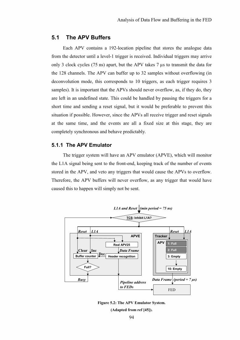
Analysis of Data Flow and Buffering in the FED
94
5.1 The APV Buffers
Each APV contains a 192-location pipeline that stores the analogue data
from the detector until a level-1 trigger is received. Individual triggers may arrive
only 3 clock cycles (75 ns) apart, but the APV takes 7 µs to transmit the data for
the 128 channels. The APV can buffer up to 32 samples without overflowing (in
deconvolution mode, this corresponds to 10 triggers, as each trigger requires 3
samples). It is important that the APVs should never overflow, as, if they do, they
are left in an undefined state. This could be handled by pausing the triggers for a
short time and sending a reset signal, but it would be preferable to prevent this
situation if possible. However, since the APVs all receive trigger and reset signals
at the same time, and the events are all a fixed size at this stage, they are
completely synchronous and behave predictably.
5.1.1 The APV Emulator
The trigger system will have an APV emulator (APVE), which will monitor
the L1A signal being sent to the front-end, keeping track of the number of events
stored in the APV, and veto any triggers that would cause the APVs to overflow.
Therefore, the APV buffers will never overflow, as any trigger that would have
caused this to happen will simply not be sent.
Tracker
APV 1: Full
2: Full
3: Empty
10: Empty
L1A and Reset (min period = 75 ns)
Data Frame (period = 7 µs)
Real APV25
Buffer counter
Reset
Data Frame
Pipeline address to FEDs
Busy
Dec
L1A
Inc
Full?
Header recognition
APVE
Clear
Reset L1A
TCS: Inhibit L1A?
FED
Figure 5.2: The APV Emulator System.
(Adapted from ref [45]).
Analysis of Data Flow and Buffering in the FED
95
An overview of the APVE is shown in figure 5.2. It receives the same L1A
and reset signals that are sent to the detector front-end. It contains a real APV25,
logic to recognise an output frame, and a counter that keeps track of the number of
events stored in the APV buffers [45]. On receipt of a level-1 trigger, the buffer
counter is incremented, and when a frame is recognised on the output from the
APV, the counter is decremented. When the buffer counter reaches the maximum
level (10 in deconvolution mode, 32 in peak mode), the busy signal is asserted,
which blocks any further triggers until the buffer levels decrease. If a trigger
causes the buffer to become full, the trigger crate must receive the busy signal
before the next trigger can be sent, and since consecutive triggers can be as close
as three clock cycles (75 ns) apart, the APVE has to be extremely fast. For this
reason it will be located in the trigger crate to keep the wiring distances as short as
possible.
A useful side effect of using a real APV in the APVE is that the correct
pipeline address in the APV header can be known. If this golden header is
transmitted to the FEDs, then the received APV headers can be crosschecked with
this header – on loss of synchronisation an error can be flagged. If the single APV
fails, the APVE could block all CMS triggers indefinitely. To prevent the APV
being a single point of failure, it may be possible to use three APVs with majority
logic for added security.
5.2 Modelling the FED
The data flow in the FED is not so simple, because of the zero-suppression
that takes place. The amount by which the data can be compressed depends on the
occupancy, which varies over the different channels, and from event to event.
A program was written in C++ to model the flow of data within the FED.
Several assumptions were made, in order to keep the simulation simple and fast
enough to generate a useful amount of data in a reasonable time. Only one
channel of a front-end FPGA is simulated. There is no need to simulate all eight
front-end FPGAs, as they are all doing the same thing in parallel, and each is
connected to the back end FPGA individually via a point-to-point link. Similarly,
the 12 channels within a front-end FPGA all behave alike. The only difference
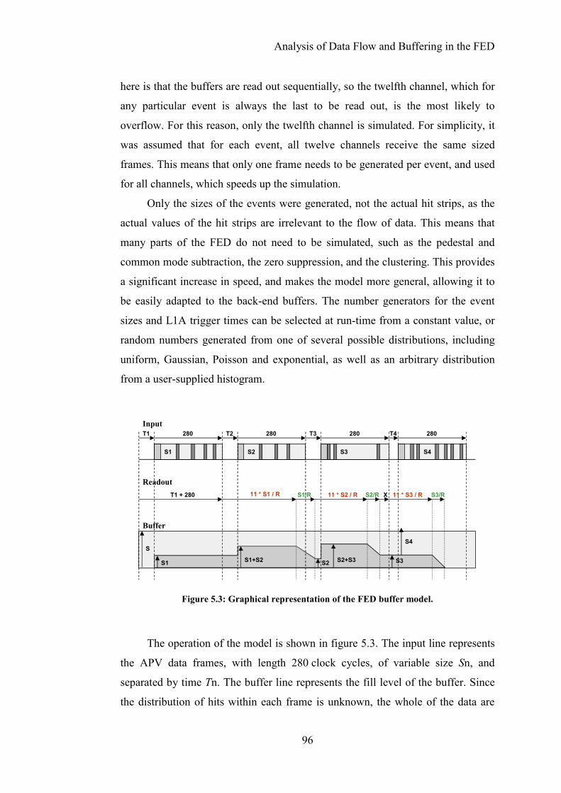
Analysis of Data Flow and Buffering in the FED
96
here is that the buffers are read out sequentially, so the twelfth channel, which for
any particular event is always the last to be read out, is the most likely to
overflow. For this reason, only the twelfth channel is simulated. For simplicity, it
was assumed that for each event, all twelve channels receive the same sized
frames. This means that only one frame needs to be generated per event, and used
for all channels, which speeds up the simulation.
Only the sizes of the events were generated, not the actual hit strips, as the
actual values of the hit strips are irrelevant to the flow of data. This means that
many parts of the FED do not need to be simulated, such as the pedestal and
common mode subtraction, the zero suppression, and the clustering. This provides
a significant increase in speed, and makes the model more general, allowing it to
be easily adapted to the back-end buffers. The number generators for the event
sizes and L1A trigger times can be selected at run-time from a constant value, or
random numbers generated from one of several possible distributions, including
uniform, Gaussian, Poisson and exponential, as well as an arbitrary distribution
from a user-supplied histogram.
The operation of the model is shown in figure 5.3. The input line represents
the APV data frames, with length 280 clock cycles, of variable size Sn, and
separated by time Tn. The buffer line represents the fill level of the buffer. Since
the distribution of hits within each frame is unknown, the whole of the data are
280 280T2 T3
S1
T1
S2 S3
280
S1 S1+S2
11 * S1 / R S1/RT1 + 280 11 * S2 / R
S2 S2+S3
S2/R
S4
T4
S4
11 * S3 / R S3/R
280
S3
X
Input
Readout
Buffer
S
Figure 5.3: Graphical representation of the FED buffer model.

Analysis of Data Flow and Buffering in the FED
97
stored in the buffer at the start of the event, and the buffer level jumps up by the
size of the event. Only once the whole of the event is stored in the buffer, at the
end of the frame, can the data start being read out. However, since we are looking
at the last of the twelve channels, the eleven other channels must be read out first.
The status of the readout link is represented by the readout line. After the end of
the first event, the first eleven channels are read out, taking a time per channel
equal to the size of the event divided by the output rate of the link. Only after this
can the twelfth channel be read out, and during this time, the buffer level falls
linearly.
If an event is too large to fit in the remaining buffer capacity (as in event 4
in the diagram), the whole event is discarded. A counter keeps track of the number
of lost events, and at the end of the run, this is displayed and saved to a file for
later analysis.
5.2.1 Source Data
In order for the simulation to be useful, the generated event sizes should be
similar to the actual distribution of event sizes in the tracker, so a histogram of
event sizes was obtained from Monte-Carlo simulation [46] (see figure 5.4). The
graph shows the frequency of event sizes per 768-strip detector (read out by 6
APVs) in the inner layer of the tracker, where the occupancy is highest. As only
the total number of hit strips per event is known, but not the distribution of the
strips within each event, it is not possible to obtain the exact distribution per APV.
600
400
200
0
Eve
nts
100806040200Event Size
Entries: 6709Mean: 23.76Std Dev: 12.93
Figure 5.4: Distribution of event sizes in strips per detector, from Monte-Carlo.
(Adapted from ref [46])
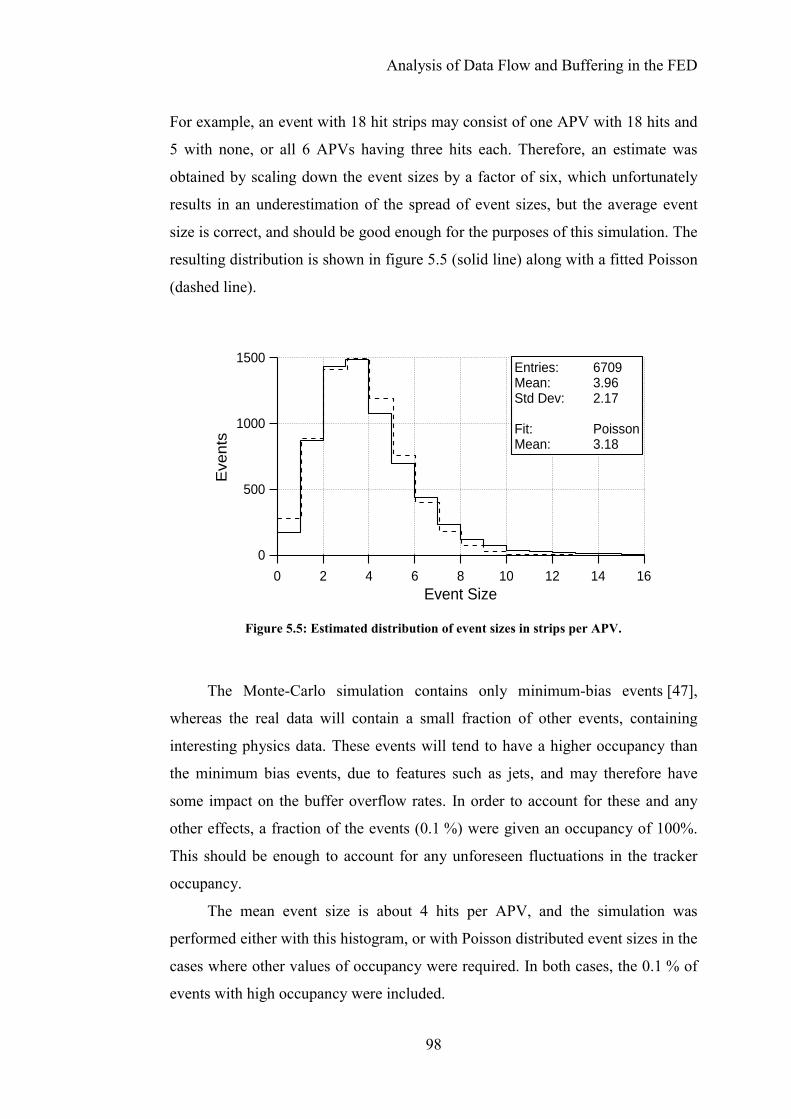
Analysis of Data Flow and Buffering in the FED
98
For example, an event with 18 hit strips may consist of one APV with 18 hits and
5 with none, or all 6 APVs having three hits each. Therefore, an estimate was
obtained by scaling down the event sizes by a factor of six, which unfortunately
results in an underestimation of the spread of event sizes, but the average event
size is correct, and should be good enough for the purposes of this simulation. The
resulting distribution is shown in figure 5.5 (solid line) along with a fitted Poisson
(dashed line).
The Monte-Carlo simulation contains only minimum-bias events [47],
whereas the real data will contain a small fraction of other events, containing
interesting physics data. These events will tend to have a higher occupancy than
the minimum bias events, due to features such as jets, and may therefore have
some impact on the buffer overflow rates. In order to account for these and any
other effects, a fraction of the events (0.1 %) were given an occupancy of 100%.
This should be enough to account for any unforeseen fluctuations in the tracker
occupancy.
The mean event size is about 4 hits per APV, and the simulation was
performed either with this histogram, or with Poisson distributed event sizes in the
cases where other values of occupancy were required. In both cases, the 0.1 % of
events with high occupancy were included.
1500
1000
500
0
Eve
nts
1614121086420Event Size
Entries: 6709Mean: 3.96Std Dev: 2.17 Fit: PoissonMean: 3.18
Figure 5.5: Estimated distribution of event sizes in strips per APV.
Analysis of Data Flow and Buffering in the FED
99
Only the front-end buffer is modelled. However, by suitable changes to the
parameters of the simulation, i.e. data rates and buffer size, it is possible to obtain
a reasonable simulation of the back-end data buffer. The header buffer can be
modelled by counting the number of events in the back-end data buffer (including
‘lost’ events, which are still stored, but given a size of 0), as opposed to the total
volume of data, because the data stored in the header buffer have a fixed size per
event. The actual number of events in the header buffer could be greater than the
number of events in the data buffer, if L1A signals have been received but the
frames from the APVs have not yet arrived at the FED, so the peak level of the
header buffer may be underestimated. However, this difference will be limited by
the number of events that can be buffered by the APV, which is 10 in
deconvolution mode, or 32 in peak mode, and is negligible when compared to the
total buffer size.
5.3 Simulation Results
5.3.1 Zero-Suppression Mode
In normal FED operation, the zero-suppression mode is used. Level-1
triggers are sent at a maximum average rate of 100 kHz with a Poisson
distribution, and the sizes of the events transmitted to the DAQ depend on their
occupancy.
Front-End Buffer
The fraction of events lost due to overflow in the front-end buffer is shown
in figure 5.6, for several buffer sizes, and as a function of the data rate of the link
to the back-end FPGA, assuming that this rate can be sustained, i.e. the back-end
buffer is not getting full. The event sizes are all generated from the histogram of
Monte Carlo events, and the trigger rate is assumed to be a worst-case 140 kHz,
corresponding to back-to-back events from the APV. The results for three
different buffer sizes are plotted; the actual buffer size is about 4 kbytes (the solid
line), corresponding to about 250 events in the highest occupancy inner tracker
layer.
Analysis of Data Flow and Buffering in the FED
100
The actual data rate between the front and back-end FPGAs is 80 Mbyte/s,
which is well off the end of the x-axis of the graph. The curves fall extremely
quickly, and at 80 Mbyte/s there is effectively a zero probability of buffer
overflow.
If we fix the readout rate at 80 Mbyte/s, and instead vary the occupancy, we
get the results shown in figure 5.7. Again, for the worst-case inner-tracker
occupancy of 4 %, there is a virtually zero probability of buffer overflow.
Obviously this still assumes that the readout rate of 80 Mbyte/s can be sustained
indefinitely; to verify under what conditions this is true, we need to look more
closely at the back-end buffer.
1E-8
1E-7
1E-6
1E-5
1E-4
1E-3
1E-2
1E-1
1E+0
20 25 30 35 40Output Rate(MB/s)
Frac
tion
of E
vent
s Lo
st 2k4k8k
Figure 5.6: Zero-suppression, front-end: events lost vs. output rate.
Analysis of Data Flow and Buffering in the FED
101
Back-End Buffer
The maximum data rate between the front-end and back-end FPGAs is so
high, relative to the average data rate, that the front-end buffers will effectively
never overflow, as long as there is space in the back-end data buffer. If some of
the parameters of the simulation are changed, i.e. the buffer size and data output
rate, reasonably good results may be obtained for the back-end data buffer, as well
as for the front-end buffers.
The results were calculated for buffer sizes of 1 Mbyte and 100 kbyte (see
figure 5.8). The buffer was originally planned to be 1 Mbyte, but was later
increased to 2 Mbyte because two external 1 Mbyte RAM chips were used in
order to reduce the data transfer rate to each chip and simplify the design. It can
be seen that there is virtually no difference between the two buffer sizes,
indicating that any further increase in buffer size should have no significant effect,
and the 1 Mbyte (and therefore also 2 Mbyte) buffer is large enough.
1E-8
1E-7
1E-6
1E-5
1E-4
1E-3
1E-2
1E-1
1E+0
0 5 10 15 20Occupancy (%)
Frac
tion
of E
vent
s Lo
st2k4k8k
Figure 5.7: Zero-suppression, front-end: events lost vs. occupancy.
Analysis of Data Flow and Buffering in the FED
102
In order to handle a tracker occupancy of 4 %, it is necessary that the DAQ
link can sustain a data rate of at least 260 Mbyte/s, which is higher than the
specified maximum average rate of 200 Mbyte/s. However, this was using back-
to-back frames at 140 kHz; when 100 kHz Poisson level-1 triggers are used this
rate falls to 185 Mbyte/s, which is within the specified range. Also the average
occupancy over any individual FED should be lower than 4 %, as each FED will
handle a mixture of high-occupancy (inner barrel) and lower occupancy layers.
In figure 5.9, the overflow rate of the back-end buffer is plotted as a
function of the tracker occupancy, for three different output rates, and using back-
to-back (140 kHz) frames. It can be seen that the maximum occupancy before the
back-end buffer starts overflowing depends strongly on the output data rate.
1E-8
1E-7
1E-6
1E-5
1E-4
1E-3
1E-2
1E-1
1E+0
100 200 300 400Output Rate(MB/s)
Frac
tion
of E
vent
s Lo
st100k1M
Figure 5.8: Zero-suppression, back-end: events lost vs. output rate.

Analysis of Data Flow and Buffering in the FED
103
The maximum occupancy was found for several output rates, both for back-
to-back frames (140 kHz) and for 100 kHz Poisson triggers, and the results are
shown in figure 5.10. The maximum occupancy was found to the nearest 0.1 %,
such that no events were lost in a total run of 108 events. At a data output rate of
200 Mbyte/s and with 100 kHz Poisson level-1 triggers the FED can just cope
with an occupancy of 4 %. However, as mentioned earlier, the actual occupancy
will be less than this, since each FED will handle a mixture of high and low-
occupancy layers.
1E-8
1E-7
1E-6
1E-5
1E-4
1E-3
1E-2
1E-1
1E+0
0 2 4 6 8 10Occupancy
(%)
Frac
tion
of E
vent
s Lo
st
100 MB/s200 MB/s400 MB/s
Figure 5.9: Zero-suppression, back-end: events lost vs. occupancy.
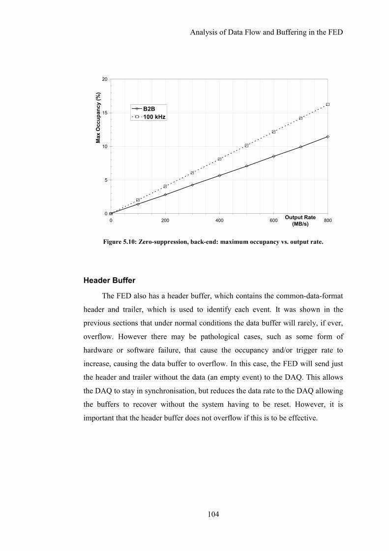
Analysis of Data Flow and Buffering in the FED
104
Header Buffer
The FED also has a header buffer, which contains the common-data-format
header and trailer, which is used to identify each event. It was shown in the
previous sections that under normal conditions the data buffer will rarely, if ever,
overflow. However there may be pathological cases, such as some form of
hardware or software failure, that cause the occupancy and/or trigger rate to
increase, causing the data buffer to overflow. In this case, the FED will send just
the header and trailer without the data (an empty event) to the DAQ. This allows
the DAQ to stay in synchronisation, but reduces the data rate to the DAQ allowing
the buffers to recover without the system having to be reset. However, it is
important that the header buffer does not overflow if this is to be effective.
0
5
10
15
20
0 200 400 600 800Output Rate(MB/s)
Max
Occ
upan
cy (%
)
B2B100 kHz
Figure 5.10: Zero-suppression, back-end: maximum occupancy vs. output rate.
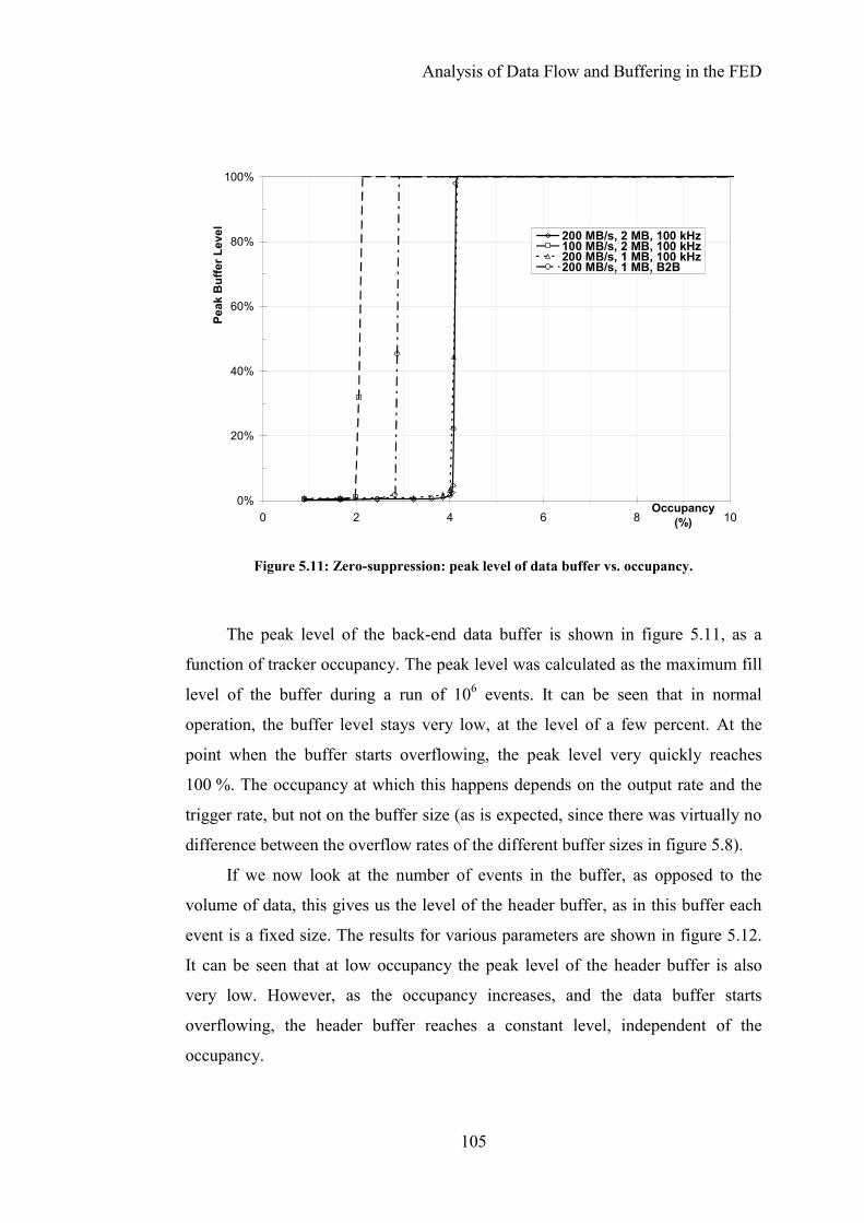
Analysis of Data Flow and Buffering in the FED
105
The peak level of the back-end data buffer is shown in figure 5.11, as a
function of tracker occupancy. The peak level was calculated as the maximum fill
level of the buffer during a run of 106 events. It can be seen that in normal
operation, the buffer level stays very low, at the level of a few percent. At the
point when the buffer starts overflowing, the peak level very quickly reaches
100 %. The occupancy at which this happens depends on the output rate and the
trigger rate, but not on the buffer size (as is expected, since there was virtually no
difference between the overflow rates of the different buffer sizes in figure 5.8).
If we now look at the number of events in the buffer, as opposed to the
volume of data, this gives us the level of the header buffer, as in this buffer each
event is a fixed size. The results for various parameters are shown in figure 5.12.
It can be seen that at low occupancy the peak level of the header buffer is also
very low. However, as the occupancy increases, and the data buffer starts
overflowing, the header buffer reaches a constant level, independent of the
occupancy.
0%
20%
40%
60%
80%
100%
0 2 4 6 8 10Occupancy
(%)
Peak
Buf
fer L
evel 200 MB/s, 2 MB, 100 kHz
100 MB/s, 2 MB, 100 kHz200 MB/s, 1 MB, 100 kHz200 MB/s, 1 MB, B2B
Figure 5.11: Zero-suppression: peak level of data buffer vs. occupancy.
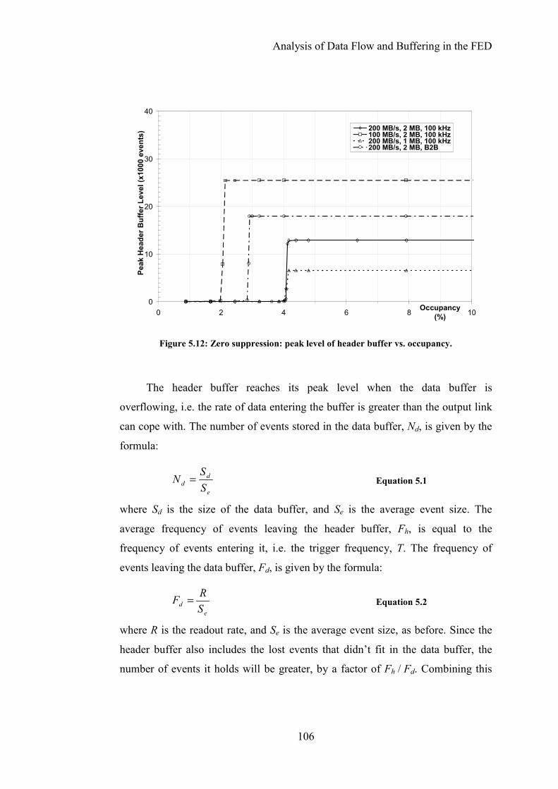
Analysis of Data Flow and Buffering in the FED
106
The header buffer reaches its peak level when the data buffer is
overflowing, i.e. the rate of data entering the buffer is greater than the output link
can cope with. The number of events stored in the data buffer, Nd, is given by the
formula:
e
dd S
SN = Equation 5.1
where Sd is the size of the data buffer, and Se is the average event size. The
average frequency of events leaving the header buffer, Fh, is equal to the
frequency of events entering it, i.e. the trigger frequency, T. The frequency of
events leaving the data buffer, Fd, is given by the formula:
ed S
RF = Equation 5.2
where R is the readout rate, and Se is the average event size, as before. Since the
header buffer also includes the lost events that didn’t fit in the data buffer, the
number of events it holds will be greater, by a factor of Fh / Fd. Combining this
0
10
20
30
40
0 2 4 6 8 10Occupancy(%)
Peak
Hea
der B
uffe
r Lev
el (x
1000
eve
nts)
200 MB/s, 2 MB, 100 kHz100 MB/s, 2 MB, 100 kHz200 MB/s, 1 MB, 100 kHz200 MB/s, 2 MB, B2B
Figure 5.12: Zero suppression: peak level of header buffer vs. occupancy.
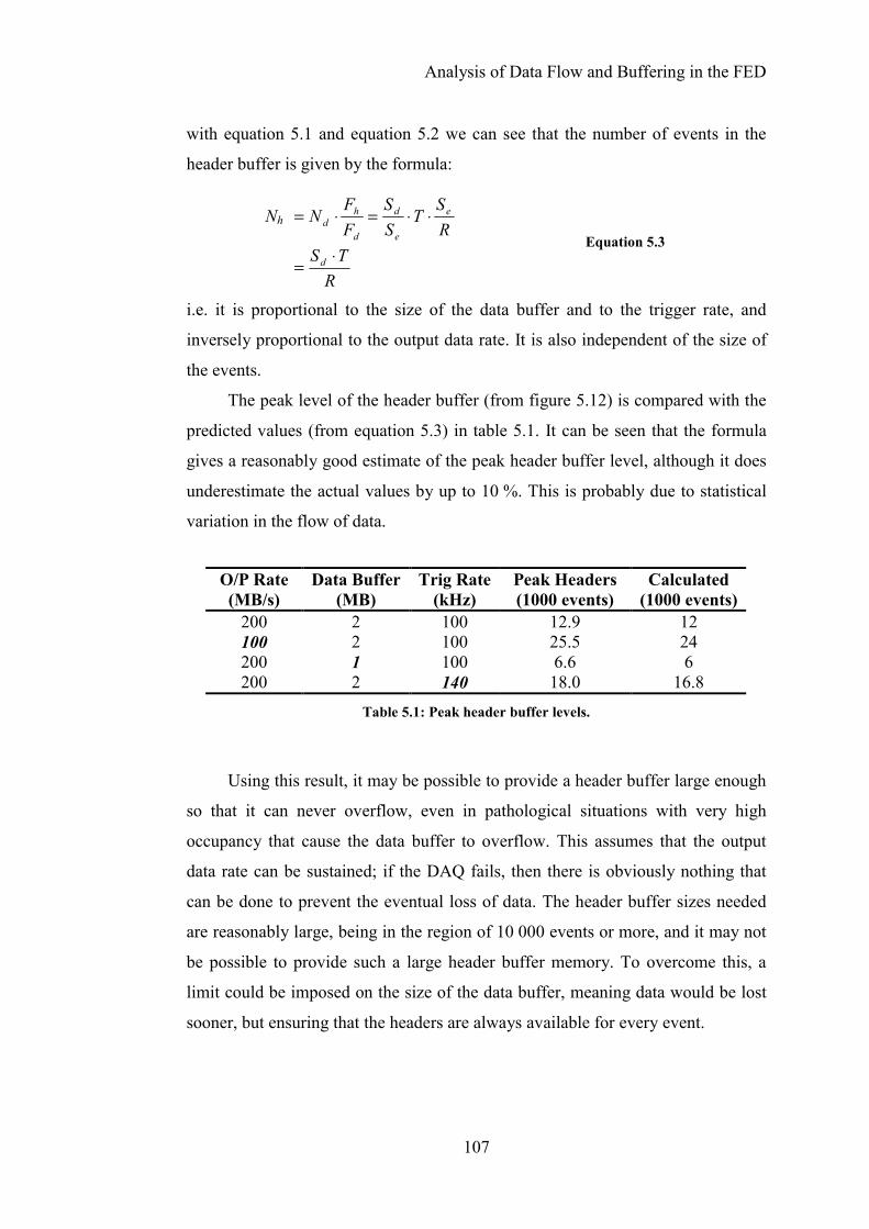
Analysis of Data Flow and Buffering in the FED
107
with equation 5.1 and equation 5.2 we can see that the number of events in the
header buffer is given by the formula:
Nh RS
TSS
FF
N e
e
d
d
hd ⋅⋅=⋅=
RTSd ⋅
= Equation 5.3
i.e. it is proportional to the size of the data buffer and to the trigger rate, and
inversely proportional to the output data rate. It is also independent of the size of
the events.
The peak level of the header buffer (from figure 5.12) is compared with the
predicted values (from equation 5.3) in table 5.1. It can be seen that the formula
gives a reasonably good estimate of the peak header buffer level, although it does
underestimate the actual values by up to 10 %. This is probably due to statistical
variation in the flow of data.
Using this result, it may be possible to provide a header buffer large enough
so that it can never overflow, even in pathological situations with very high
occupancy that cause the data buffer to overflow. This assumes that the output
data rate can be sustained; if the DAQ fails, then there is obviously nothing that
can be done to prevent the eventual loss of data. The header buffer sizes needed
are reasonably large, being in the region of 10 000 events or more, and it may not
be possible to provide such a large header buffer memory. To overcome this, a
limit could be imposed on the size of the data buffer, meaning data would be lost
sooner, but ensuring that the headers are always available for every event.
O/P Rate (MB/s)
Data Buffer(MB)
Trig Rate(kHz)
Peak Headers (1000 events)
Calculated (1000 events)
200 2 100 12.9 12 100 2 100 25.5 24 200 1 100 6.6 6 200 2 140 18.0 16.8
Table 5.1: Peak header buffer levels.

Analysis of Data Flow and Buffering in the FED
108
5.3.2 Raw-Data Mode
In certain conditions, such as the early detector study and calibration runs,
and during heavy-ion runs, the FED will be run in raw data mode. In this mode,
zero-suppression of the data will not be performed, and the entire events will be
sent to the DAQ. The events will therefore all be the same size, and much larger
than in normal operation. In order for the readout system to be able to cope with
this, the level-1 trigger rate will have to be much lower than in normal operation.
Front-End Buffer
The results for the front-end buffer are shown in figure 5.13, as a function of
the average level-1 accept rate, for three different buffer sizes. The actual buffer
size is 4 kbyte, corresponding to 16 raw events. It can be seen that up to a trigger
rate of 10 kHz, and with a 4 kbyte buffer, less than one event is lost per 108.
1E-8
1E-7
1E-6
1E-5
1E-4
1E-3
1E-2
1E-1
1E+0
1 10 100Trigger Rate
(kHz)
Frac
tion
of E
vent
s Lo
st 2k4k8k
Figure 5.13: Raw data, front-end: events lost vs. trigger rate.

Analysis of Data Flow and Buffering in the FED
109
Back-End Buffer
The results for the back-end buffer are shown in figure 5.14, as a function of
the level-1 accept rate, and for three output rates.
The maximum level-1 trigger rate depends on the output rate, and at
200 Mbyte/s, the FED can cope with trigger rates up to just under 8 kHz. The
graph in figure 5.15 shows the maximum level-1 accept rate as a function of the
data output rate.
1E-8
1E-7
1E-6
1E-5
1E-4
1E-3
1E-2
1E-1
1E+0
1 10 100Trigger Rate
(kHz)
Frac
tion
of E
vent
s Lo
st 100 MB/s200 MB/s400 MB/s
Figure 5.14: Raw data, back-end: events lost vs. trigger rate.
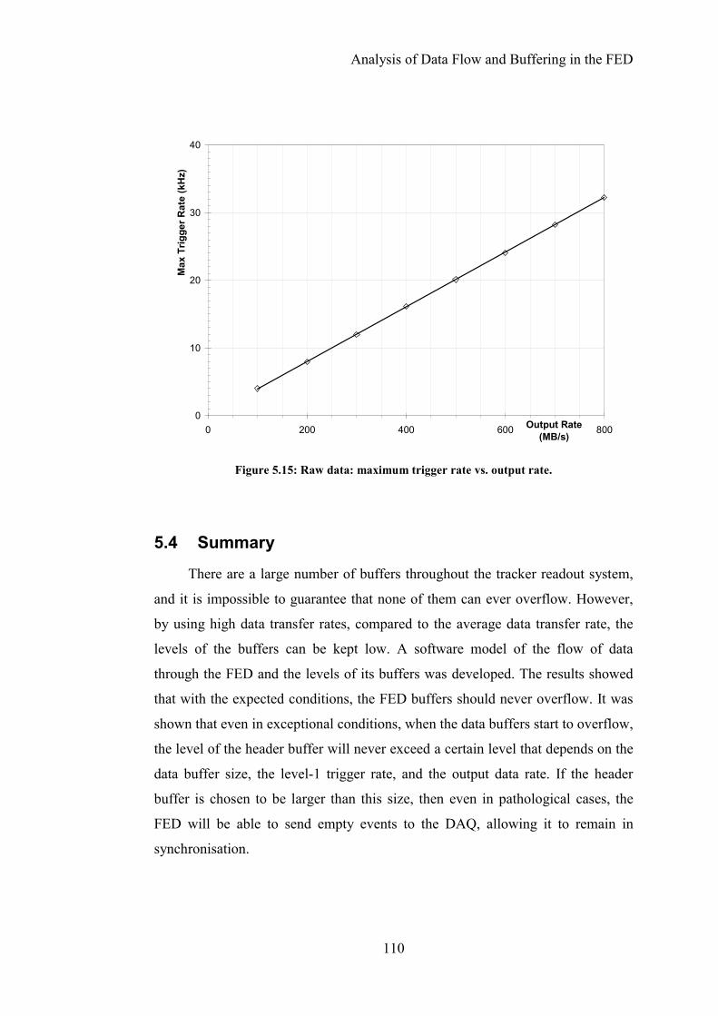
Analysis of Data Flow and Buffering in the FED
110
5.4 Summary
There are a large number of buffers throughout the tracker readout system,
and it is impossible to guarantee that none of them can ever overflow. However,
by using high data transfer rates, compared to the average data transfer rate, the
levels of the buffers can be kept low. A software model of the flow of data
through the FED and the levels of its buffers was developed. The results showed
that with the expected conditions, the FED buffers should never overflow. It was
shown that even in exceptional conditions, when the data buffers start to overflow,
the level of the header buffer will never exceed a certain level that depends on the
data buffer size, the level-1 trigger rate, and the output data rate. If the header
buffer is chosen to be larger than this size, then even in pathological cases, the
FED will be able to send empty events to the DAQ, allowing it to remain in
synchronisation.
0
10
20
30
40
0 200 400 600 800Output Rate(MB/s)
Max
Trig
ger R
ate
(kH
z)
Figure 5.15: Raw data: maximum trigger rate vs. output rate.

111
Chapter 6: Perspectives
6.1 FED Schedule The LHC is due to start operating in 2007 and the 440 FEDs must be ready
by then. A first batch of 2 FEDs is currently under construction. The board level
routing is in its final stages, and the PCB manufacture and board assembly are
expected to be completed by the end of 2002. The prototype FEDs will then be
thoroughly tested at RAL and Imperial College over the following months. After
preliminary tests are completed, the optical receivers will be mounted on the
boards, and also tested. By mid 2003 there will be a design review, and any
necessary design changes will then be implemented.
The construction of a second batch of 10 FEDs will start following the
review of the previous batch. These are expected to be assembled, production
tested, and delivered to CERN by the end of 2003. Field tests of these FEDs will
then be carried out until the end of 2004.
By this time, the procurement and production of the remaining FEDs will
have started. FED assembly is scheduled for completion by mid 2005. From that
point onwards, field tests at CERN will run until mid 2006, and the installation at
CMS will start in parallel with these tests and should be completed by the end of
2006, in time for the first LHC collisions, scheduled for mid 2007. This is a
reasonably tight schedule, and may have to adapt to external circumstances, so
effort will be needed to ensure it stays on track.
6.2 FED Testing
The testing of the FEDs will consist of a number of stages. The PCB
manufacturer should perform bare-board tests, and on delivery of the PCBs to
RAL they will be visually inspected and simple tests for short-circuits will be
performed. The boards will then be assembled, and should be visually inspected
by the assembly company. On delivery to RAL, each FED will be given a unique
3-digit serial number, with each board labelled and programmed electronically,
allowing them to be traced individually. The first pair of FEDs will also be
thoroughly inspected visually for missing or incorrect components, solder bridges,
Perspectives
112
and other general visible damage, as well as the power rails being tested for short
circuits.
6.2.1 JTAG and Boundary Scan Testing
The boards will then be ready to be powered-up for the first time, and
voltages will be measured at specific points and the results recorded. The next
step will be to verify that the JTAG chain is operational, and all the correct
devices are present in this chain. A boundary scan test can then be performed,
which will verify the connections between all devices in the JTAG chain. The
FPGAs themselves will then be configured with simple designs, via the JTAG
chain, to verify their basic functionality. During large-scale production runs, these
JTAG tests will be performed by the assembly company.
6.2.2 Basic Analogue Tests
The analogue and digital parts of the FEDs will be tested using Xilinx
Chipscope Integrated Logic Analyzer (ILA). This tool embeds logic analysis
cores inside the FPGAs, allowing external ports and internal signals of the FPGA
to be monitored via the JTAG port. The FPGAs will be configured with logic to
distribute the relevant clocks across the board, and the delay FPGAs will
additionally contain a Chipscope ILA on the ADC inputs. Signals can then be
injected into the analogue circuitry, and the results read out via the JTAG port. At
this point, one of the first two FEDs may be sent to Imperial College so that the
remaining tests may be carried out in parallel.
6.2.3 Basic Digital Tests
Once the functionality of the board has been verified, then tests can begin
on the firmware. The first FPGAs to be tested will be the delay FPGAs. They will
be configured with their standard firmware, and the front-end FPGAs will be
loaded with a Chipscope ILA connected to the raw data input. APV frame-like
data will then be injected into the analogue section, allowing the verification of
both the delay FPGA firmware, and the double data rate connection between the
FPGAs. The front-end FPGAs will then be loaded with their standard firmware
Perspectives
113
and the back-end FPGA configured with a Chipscope ILA so that the front-end
FPGA firmware can be verified.
The next step will be to load a basic VME interface into the VME FPGA,
and plug the board into a VME crate. A simple program will be run on the crate
controller to test the writing and reading of internal registers, using a VME bus
analyser to verify signals on the VME bus. The interface between the VME and
the other (delay, front-end and back-end) FPGAs can then be tested.
6.2.4 More Advanced Tests
A FED testing system is being developed at Imperial College. This will
provide realistic input signals, in optical form, including the TTC clock and L1A
signals. The output from the FED will be sent back to the testing system, allowing
this to be compared to expected output data. The testing system is based around a
PC, with a PCI-64 bus for the S-LINK64 receiver. This will eventually allow the
testing process to be semi-automated, which will be necessary when testing large
numbers of production FEDs.
6.3 Conclusions
Firmware code for the FED was developed in VHDL, including a testbench
for verifying its functionality. It was designed with the back-end FPGA of the
tracker FED in mind, but is general enough to be included in other systems. In this
way, the same VHDL code will be used in the front-end drivers of all the CMS
subdetectors, thus ensuring uniformity across the readout system.
The study into the data flow and buffering in the FED showed that in
normal operating conditions, the FED will never overflow. The maximum tracker
occupancy before overflow occurs was calculated as a function of output data rate,
using both 100 kHz random triggers, and 140 kHz back-to-back triggers. At an
output rate of 200 Mbyte/s these results were 4 % and 2.5 % respectively. For raw
data mode, the maximum trigger rate was calculated as a function of the output
data rate, and at 200 Mbyte/s this was found to be just under 8 kHz.
It was shown that the speed of the links between the front and back-end
FPGAs was more important than the buffer sizes in preventing overflows in the
Perspectives
114
front-end buffers. Because of this, a link speed of 80 Mbyte/s was chosen over the
other possibility of 40 Mbyte/s.
In addition, the header buffer was investigated. It was found that for any
given trigger rate, buffer size, and output data rate, a maximum trigger buffer
level could be calculated. The firmware for the back-end FPGA of the FED is still
under development, and if enough memory is available for the necessary header
buffer size, this may be exploited to provide a header buffer that can never
overflow, no matter how high the occupancy, as long as the DAQ continues to
accept data.

115
Appendix A: Common Data Format Implementation The VHDL source code for the common data format header and trailer building
block from the FED back-end FPGA is listed. It was developed using Mentor Graphics
FPGA Advantage, which includes HDL Designer (previously called Renoir) for code
entry, ModelSim for simulation, and Leonardo Spectrum for synthesis. All of the
modules are written in VHDL, apart from the top-level FED_DATA_FORMAT block,
which is a block-diagram (shown in figure 4.12), and therefore the listing for this block
contains the generated VHDL code.
A.1 fed_data_format.vhd -- hds header_start---- VHDL Entity FED_DATA_FORMAT.data_format.symbol---- Created:-- by - corrinep.UNKNOWN (EMLYN)-- at - 10:58:39 10/26/02---- Generated by Mentor Graphics' HDL Designer(TM) 2002.1a (Build 22)---- hds header_endLIBRARY ieee;USE ieee.std_logic_1164.ALL;
ENTITY data_format ISGENERIC(
fifo_addr_bits : natural := 9;length_at_start : boolean := true
);PORT(
clk : IN std_logic;data_bx_id : IN std_logic_vector (11 DOWNTO 0);data_evt_lgth : IN std_logic_vector (23 DOWNTO 0);data_evt_stat : IN std_logic_vector (7 DOWNTO 0);data_evt_ty : IN std_logic_vector (3 DOWNTO 0);data_in : IN std_logic_vector (63 DOWNTO 0);data_in_en : IN std_logic;data_lv1_id : IN std_logic_vector (23 DOWNTO 0);data_source_id : IN std_logic_vector (11 DOWNTO 0);linkfull : IN std_logic;rd_start : IN std_logic;rd_stop : IN std_logic;reset : IN std_logic;wr_start : IN std_logic;ctrl : OUT std_logic;data_out : OUT std_logic_vector (63 DOWNTO 0);data_out_en : OUT std_logic;rd_ready : OUT std_logic;wr_ready : OUT std_logic

Common Data Format Implementation
116
);
-- Declarations
END data_format ;
-- hds interface_end---- VHDL Architecture FED_DATA_FORMAT.data_format.fed_data_format---- Created:-- by - corrinep.UNKNOWN (EMLYN)-- at - 10:58:41 10/26/02---- Generated by Mentor Graphics' HDL Designer(TM) 2002.1a (Build 22)--LIBRARY ieee;USE ieee.std_logic_1164.ALL;
LIBRARY FED_DATA_FORMAT;
ARCHITECTURE fed_data_format OF data_format IS
-- Architecture declarations
-- Internal signal declarationsSIGNAL data_out_sel : std_logic_vector(1 DOWNTO 0);SIGNAL empty : std_logic;SIGNAL full : std_logic;SIGNAL header_in : std_logic_vector(63 DOWNTO 0);SIGNAL rd_data : std_logic_vector(63 DOWNTO 0);SIGNAL rd_en : std_logic;SIGNAL wr_data : std_logic_vector(63 DOWNTO 0);SIGNAL wr_en : std_logic;
-- Component DeclarationsCOMPONENT builderPORT (
clk : IN std_logic ;data_bx_id : IN std_logic_vector (11 DOWNTO 0);data_evt_stat : IN std_logic_vector (7 DOWNTO 0);data_evt_ty : IN std_logic_vector (3 DOWNTO 0);data_lv1_id : IN std_logic_vector (23 DOWNTO 0);data_source_id : IN std_logic_vector (11 DOWNTO 0);wr_start : IN std_logic ;rd_data : IN std_logic_vector (63 DOWNTO 0);reset : IN std_logic ;rd_start : IN std_logic ;data_out : OUT std_logic_vector (63 DOWNTO 0);data_out_sel : OUT std_logic_vector (1 DOWNTO 0);rd_en : OUT std_logic ;wr_ready : OUT std_logic ;wr_data : OUT std_logic_vector (63 DOWNTO 0);wr_en : OUT std_logic ;data_evt_lgth : IN std_logic_vector (23 DOWNTO 0);rd_ready : OUT std_logic ;full : IN std_logic ;empty : IN std_logic ;
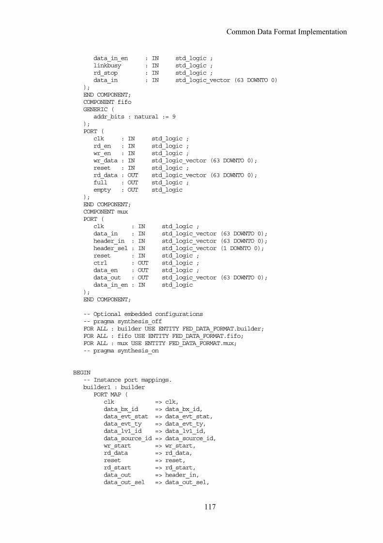
Common Data Format Implementation
117
data_in_en : IN std_logic ;linkbusy : IN std_logic ;rd_stop : IN std_logic ;data_in : IN std_logic_vector (63 DOWNTO 0)
);END COMPONENT;COMPONENT fifoGENERIC (
addr_bits : natural := 9);PORT (
clk : IN std_logic ;rd_en : IN std_logic ;wr_en : IN std_logic ;wr_data : IN std_logic_vector (63 DOWNTO 0);reset : IN std_logic ;rd_data : OUT std_logic_vector (63 DOWNTO 0);full : OUT std_logic ;empty : OUT std_logic
);END COMPONENT;COMPONENT muxPORT (
clk : IN std_logic ;data_in : IN std_logic_vector (63 DOWNTO 0);header_in : IN std_logic_vector (63 DOWNTO 0);header_sel : IN std_logic_vector (1 DOWNTO 0);reset : IN std_logic ;ctrl : OUT std_logic ;data_en : OUT std_logic ;data_out : OUT std_logic_vector (63 DOWNTO 0);data_in_en : IN std_logic
);END COMPONENT;
-- Optional embedded configurations-- pragma synthesis_offFOR ALL : builder USE ENTITY FED_DATA_FORMAT.builder;FOR ALL : fifo USE ENTITY FED_DATA_FORMAT.fifo;FOR ALL : mux USE ENTITY FED_DATA_FORMAT.mux;-- pragma synthesis_on
BEGIN-- Instance port mappings.builder1 : builder
PORT MAP (clk => clk,data_bx_id => data_bx_id,data_evt_stat => data_evt_stat,data_evt_ty => data_evt_ty,data_lv1_id => data_lv1_id,data_source_id => data_source_id,wr_start => wr_start,rd_data => rd_data,reset => reset,rd_start => rd_start,data_out => header_in,data_out_sel => data_out_sel,
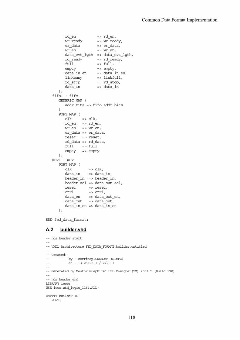
Common Data Format Implementation
118
rd_en => rd_en,wr_ready => wr_ready,wr_data => wr_data,wr_en => wr_en,data_evt_lgth => data_evt_lgth,rd_ready => rd_ready,full => full,empty => empty,data_in_en => data_in_en,linkbusy => linkfull,rd_stop => rd_stop,data_in => data_in
);fifo1 : fifo
GENERIC MAP (addr_bits => fifo_addr_bits
)PORT MAP (
clk => clk,rd_en => rd_en,wr_en => wr_en,wr_data => wr_data,reset => reset,rd_data => rd_data,full => full,empty => empty
);mux1 : mux
PORT MAP (clk => clk,data_in => data_in,header_in => header_in,header_sel => data_out_sel,reset => reset,ctrl => ctrl,data_en => data_out_en,data_out => data_out,data_in_en => data_in_en
);
END fed_data_format;
A.2 builder.vhd -- hds header_start---- VHDL Architecture FED_DATA_FORMAT.builder.untitled---- Created:-- by - corrinep.UNKNOWN (SIMPC)-- at - 13:25:28 11/12/2001---- Generated by Mentor Graphics' HDL Designer(TM) 2001.5 (Build 170)---- hds header_endLIBRARY ieee;USE ieee.std_logic_1164.ALL;
ENTITY builder ISPORT(
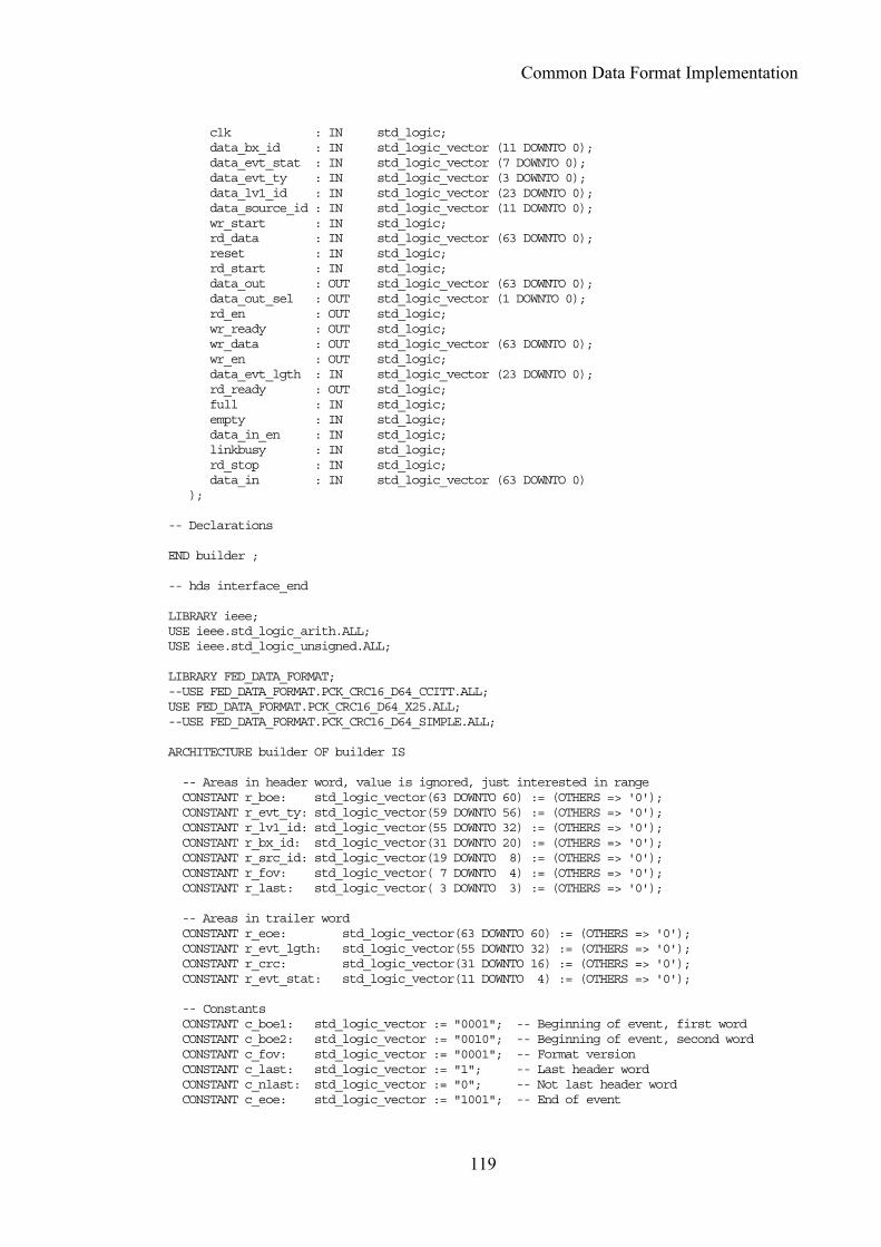
Common Data Format Implementation
119
clk : IN std_logic;data_bx_id : IN std_logic_vector (11 DOWNTO 0);data_evt_stat : IN std_logic_vector (7 DOWNTO 0);data_evt_ty : IN std_logic_vector (3 DOWNTO 0);data_lv1_id : IN std_logic_vector (23 DOWNTO 0);data_source_id : IN std_logic_vector (11 DOWNTO 0);wr_start : IN std_logic;rd_data : IN std_logic_vector (63 DOWNTO 0);reset : IN std_logic;rd_start : IN std_logic;data_out : OUT std_logic_vector (63 DOWNTO 0);data_out_sel : OUT std_logic_vector (1 DOWNTO 0);rd_en : OUT std_logic;wr_ready : OUT std_logic;wr_data : OUT std_logic_vector (63 DOWNTO 0);wr_en : OUT std_logic;data_evt_lgth : IN std_logic_vector (23 DOWNTO 0);rd_ready : OUT std_logic;full : IN std_logic;empty : IN std_logic;data_in_en : IN std_logic;linkbusy : IN std_logic;rd_stop : IN std_logic;data_in : IN std_logic_vector (63 DOWNTO 0)
);
-- Declarations
END builder ;
-- hds interface_end
LIBRARY ieee;USE ieee.std_logic_arith.ALL;USE ieee.std_logic_unsigned.ALL;
LIBRARY FED_DATA_FORMAT;--USE FED_DATA_FORMAT.PCK_CRC16_D64_CCITT.ALL;USE FED_DATA_FORMAT.PCK_CRC16_D64_X25.ALL;--USE FED_DATA_FORMAT.PCK_CRC16_D64_SIMPLE.ALL;
ARCHITECTURE builder OF builder IS
-- Areas in header word, value is ignored, just interested in rangeCONSTANT r_boe: std_logic_vector(63 DOWNTO 60) := (OTHERS => '0');CONSTANT r_evt_ty: std_logic_vector(59 DOWNTO 56) := (OTHERS => '0');CONSTANT r_lv1_id: std_logic_vector(55 DOWNTO 32) := (OTHERS => '0');CONSTANT r_bx_id: std_logic_vector(31 DOWNTO 20) := (OTHERS => '0');CONSTANT r_src_id: std_logic_vector(19 DOWNTO 8) := (OTHERS => '0');CONSTANT r_fov: std_logic_vector( 7 DOWNTO 4) := (OTHERS => '0');CONSTANT r_last: std_logic_vector( 3 DOWNTO 3) := (OTHERS => '0');
-- Areas in trailer wordCONSTANT r_eoe: std_logic_vector(63 DOWNTO 60) := (OTHERS => '0');CONSTANT r_evt_lgth: std_logic_vector(55 DOWNTO 32) := (OTHERS => '0');CONSTANT r_crc: std_logic_vector(31 DOWNTO 16) := (OTHERS => '0');CONSTANT r_evt_stat: std_logic_vector(11 DOWNTO 4) := (OTHERS => '0');
-- ConstantsCONSTANT c_boe1: std_logic_vector := "0001"; -- Beginning of event, first wordCONSTANT c_boe2: std_logic_vector := "0010"; -- Beginning of event, second wordCONSTANT c_fov: std_logic_vector := "0001"; -- Format versionCONSTANT c_last: std_logic_vector := "1"; -- Last header wordCONSTANT c_nlast: std_logic_vector := "0"; -- Not last header wordCONSTANT c_eoe: std_logic_vector := "1001"; -- End of event

Common Data Format Implementation
120
CONSTANT CRC_INIT: std_logic_vector := "1111111111111111"; -- Initial value for CRCcalculation
SIGNAL save_evt_stat: std_logic_vector(data_evt_stat'range);SIGNAL save_evt_lgth: std_logic_vector(data_evt_lgth'range);
TYPE wr_type IS (idle, writing);SIGNAL wr_state: wr_type;
TYPE rd_type IS (idle, headerstart, header, datastart, data);SIGNAL rd_state: rd_type;
BEGIN
-- builds header and trailer words and writes them to fifoproc_wr: PROCESS(clk, reset)BEGINIF (reset = '0') THEN-- reset signals to default:wr_state <= idle;wr_ready <= '0';wr_data <= (OTHERS => '0');save_evt_lgth <= (OTHERS => '0');save_evt_stat <= (OTHERS => '0');wr_en <= '0';
ELSIF (clk = '1' AND clk'event) THEN-- default assignments:wr_ready <= NOT full;wr_data <= (OTHERS => '0');wr_en <= '0';--IF (wr_state = idle) THENCASE wr_state ISWHEN idle =>IF (wr_start = '1') THENASSERT (full /= '1') REPORT "(builder: proc_wr) Writing to FIFO when full"
SEVERITY error;-- build first word (header)wr_data(r_boe'range) <= c_boe1;wr_data(r_evt_ty'range) <= data_evt_ty;wr_data(r_lv1_id'range) <= data_lv1_id;wr_data(r_bx_id'range) <= data_bx_id;wr_data(r_src_id'range) <= data_source_id;wr_data(r_fov'range) <= c_fov;wr_data(r_last'range) <= c_last; -- c_nlast if there is another header word
wr_en <= '1';-- Save data needed for trailer word
save_evt_stat <= data_evt_stat;save_evt_lgth <= data_evt_lgth;wr_state <= writing;wr_ready <= '0';
END IF;WHEN writing =>ASSERT (full /= '1') REPORT "(builder: proc_wr) Writing to FIFO when full"
SEVERITY error;ASSERT (wr_start /= '1') REPORT "(builder: proc_wr) Prepare received while
writing to FIFO" SEVERITY error;-- build second word (trailer)wr_data(r_eoe'range) <= c_eoe; -- EOEwr_data(r_evt_lgth'range) <= save_evt_lgth;wr_data(r_evt_stat'range) <= save_evt_stat;wr_en <= '1';
wr_state <= idle;--WHEN OTHERS =>-- wr_state <= idle;END CASE;
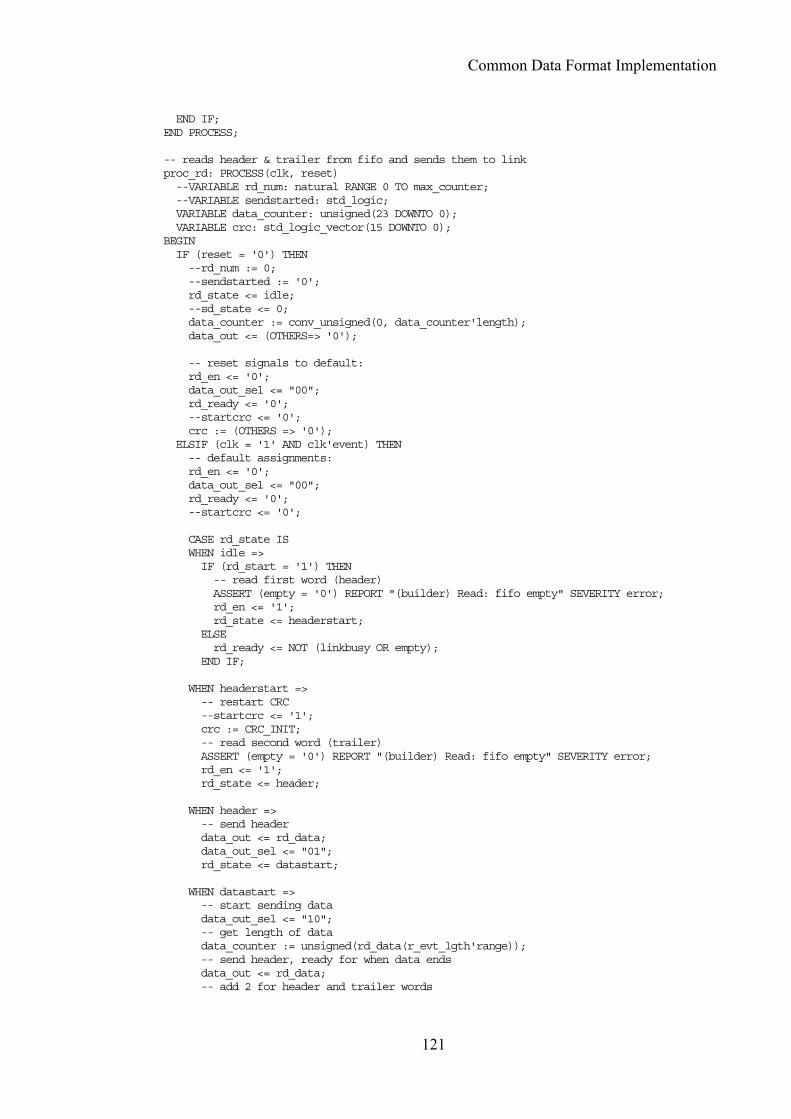
Common Data Format Implementation
121
END IF;END PROCESS;
-- reads header & trailer from fifo and sends them to linkproc_rd: PROCESS(clk, reset)--VARIABLE rd_num: natural RANGE 0 TO max_counter;--VARIABLE sendstarted: std_logic;VARIABLE data_counter: unsigned(23 DOWNTO 0);VARIABLE crc: std_logic_vector(15 DOWNTO 0);
BEGINIF (reset = '0') THEN--rd_num := 0;--sendstarted := '0';rd_state <= idle;--sd_state <= 0;data_counter := conv_unsigned(0, data_counter'length);data_out <= (OTHERS=> '0');
-- reset signals to default:rd_en <= '0';data_out_sel <= "00";rd_ready <= '0';--startcrc <= '0';crc := (OTHERS => '0');
ELSIF (clk = '1' AND clk'event) THEN-- default assignments:rd_en <= '0';data_out_sel <= "00";rd_ready <= '0';--startcrc <= '0';
CASE rd_state ISWHEN idle =>IF (rd_start = '1') THEN-- read first word (header)ASSERT (empty = '0') REPORT "(builder) Read: fifo empty" SEVERITY error;rd_en <= '1';rd_state <= headerstart;
ELSErd_ready <= NOT (linkbusy OR empty);
END IF;
WHEN headerstart =>-- restart CRC--startcrc <= '1';crc := CRC_INIT;-- read second word (trailer)ASSERT (empty = '0') REPORT "(builder) Read: fifo empty" SEVERITY error;rd_en <= '1';rd_state <= header;
WHEN header =>-- send headerdata_out <= rd_data;data_out_sel <= "01";rd_state <= datastart;
WHEN datastart =>-- start sending datadata_out_sel <= "10";-- get length of datadata_counter := unsigned(rd_data(r_evt_lgth'range));-- send header, ready for when data endsdata_out <= rd_data;-- add 2 for header and trailer words

Common Data Format Implementation
122
data_out(r_evt_lgth'range) <= std_logic_vector((rd_data(r_evt_lgth'range)) + 2);rd_state <= data;
WHEN data =>data_out_sel <= "10";IF (data_in_en = '1') THENdata_counter := data_counter - 1;crc := nextCRC16_D64(data_in, crc);
END IF;IF (data_counter <= 0) THENdata_out_sel <= "11";data_out(r_crc'range) <= crc;rd_state <= idle;
END IF;
--WHEN OTHERS =>-- rd_state <= idle;END CASE;
END IF;END PROCESS;
END builder;
A.3 fifo.vhd -- hds header_start---- VHDL Architecture FED_DATA_FORMAT.fifo.general---- Created:-- by - corrinep.UNKNOWN (SIMPC)-- at - 13:07:26 16/01/2002---- Generated by Mentor Graphics' HDL Designer(TM) 2001.5 (Build 170)---- hds header_endLIBRARY ieee;USE ieee.std_logic_1164.ALL;
ENTITY fifo ISGENERIC(
addr_bits : natural := 9);PORT(
clk : IN std_logic;rd_en : IN std_logic;wr_en : IN std_logic;wr_data : IN std_logic_vector (63 DOWNTO 0);reset : IN std_logic;rd_data : OUT std_logic_vector (63 DOWNTO 0);full : OUT std_logic;empty : OUT std_logic
);
-- Declarations
END fifo ;
-- hds interface_end
LIBRARY ieee;USE ieee.std_logic_arith.ALL;
LIBRARY FED_DATA_FORMAT;
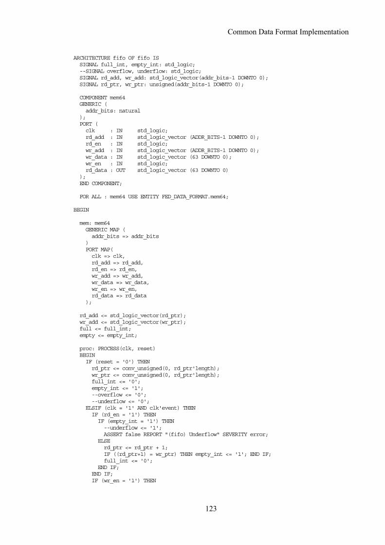
Common Data Format Implementation
123
ARCHITECTURE fifo OF fifo ISSIGNAL full_int, empty_int: std_logic;--SIGNAL overflow, underflow: std_logic;SIGNAL rd_add, wr_add: std_logic_vector(addr_bits-1 DOWNTO 0);SIGNAL rd_ptr, wr_ptr: unsigned(addr_bits-1 DOWNTO 0);
COMPONENT mem64GENERIC (addr_bits: natural
);PORT (clk : IN std_logic;rd_add : IN std_logic_vector (ADDR_BITS-1 DOWNTO 0);rd_en : IN std_logic;wr_add : IN std_logic_vector (ADDR_BITS-1 DOWNTO 0);wr_data : IN std_logic_vector (63 DOWNTO 0);wr_en : IN std_logic;rd_data : OUT std_logic_vector (63 DOWNTO 0)
);END COMPONENT;
FOR ALL : mem64 USE ENTITY FED_DATA_FORMAT.mem64;
BEGIN
mem: mem64GENERIC MAP (addr_bits => addr_bits
)PORT MAP(clk => clk,rd_add => rd_add,rd_en => rd_en,wr_add => wr_add,wr_data => wr_data,wr_en => wr_en,rd_data => rd_data
);
rd_add <= std_logic_vector(rd_ptr);wr_add <= std_logic_vector(wr_ptr);full <= full_int;empty <= empty_int;
proc: PROCESS(clk, reset)BEGINIF (reset = '0') THENrd_ptr <= conv_unsigned(0, rd_ptr'length);wr_ptr <= conv_unsigned(0, rd_ptr'length);full_int <= '0';empty_int <= '1';--overflow <= '0';--underflow <= '0';
ELSIF (clk = '1' AND clk'event) THENIF (rd_en = '1') THENIF (empty_int = '1') THEN--underflow <= '1';ASSERT false REPORT "(fifo) Underflow" SEVERITY error;
ELSErd_ptr <= rd_ptr + 1;IF ((rd_ptr+1) = wr_ptr) THEN empty_int <= '1'; END IF;full_int <= '0';
END IF;END IF;IF (wr_en = '1') THEN

Common Data Format Implementation
124
IF (full_int = '1') THEN--overflow <= '1';ASSERT false REPORT "(fifo) Overflow" SEVERITY error;
ELSEwr_ptr <= wr_ptr + 1;IF (rd_ptr = (wr_ptr+1)) THEN full_int <= '1'; END IF;empty_int <= '0';
END IF;END IF;--full <= buf_full;--empty <= buf_empty;
END IF;END PROCESS;
END fifo;
A.4 mem64_general.vhd -- hds header_start---- VHDL Architecture FED_DATA_FORMAT.mem64.general---- Created:-- by - corrinep.UNKNOWN (SIMPC)-- at - 13:17:15 11/12/2001---- Generated by Mentor Graphics' HDL Designer(TM) 2001.5 (Build 170)---- hds header_endLIBRARY ieee;USE ieee.std_logic_1164.ALL;
ENTITY mem64 ISGENERIC(
addr_bits : natural := 12);PORT(
clk : IN std_logic;rd_add : IN std_logic_vector (addr_bits-1 DOWNTO 0);rd_en : IN std_logic;wr_add : IN std_logic_vector (addr_bits-1 DOWNTO 0);wr_data : IN std_logic_vector (63 DOWNTO 0);wr_en : IN std_logic;rd_data : OUT std_logic_vector (63 DOWNTO 0)
);
-- Declarations
END mem64 ;
-- hds interface_end
LIBRARY ieee;USE ieee.numeric_std.ALL;LIBRARY FED_DATA_FORMAT;USE FED_DATA_FORMAT.Utils.ALL;
ARCHITECTURE general OF mem64 ISTYPE mem IS ARRAY(2**ADDR_BITS - 1 DOWNTO 0) OF integer;SIGNAL buf1, buf2: mem;
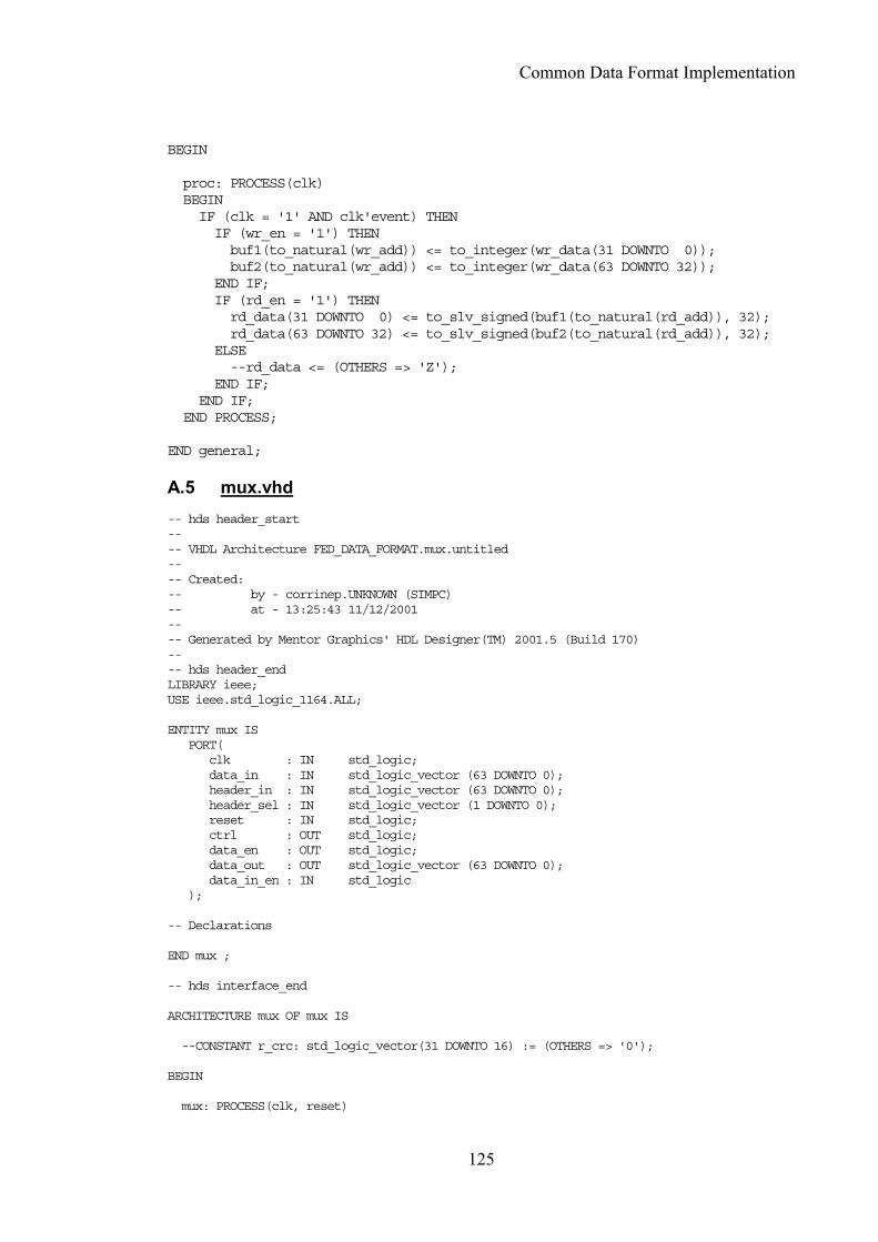
Common Data Format Implementation
125
BEGIN
proc: PROCESS(clk)BEGINIF (clk = '1' AND clk'event) THENIF (wr_en = '1') THENbuf1(to_natural(wr_add)) <= to_integer(wr_data(31 DOWNTO 0));buf2(to_natural(wr_add)) <= to_integer(wr_data(63 DOWNTO 32));
END IF;IF (rd_en = '1') THENrd_data(31 DOWNTO 0) <= to_slv_signed(buf1(to_natural(rd_add)), 32);rd_data(63 DOWNTO 32) <= to_slv_signed(buf2(to_natural(rd_add)), 32);
ELSE--rd_data <= (OTHERS => 'Z');
END IF;END IF;
END PROCESS;
END general;
A.5 mux.vhd -- hds header_start---- VHDL Architecture FED_DATA_FORMAT.mux.untitled---- Created:-- by - corrinep.UNKNOWN (SIMPC)-- at - 13:25:43 11/12/2001---- Generated by Mentor Graphics' HDL Designer(TM) 2001.5 (Build 170)---- hds header_endLIBRARY ieee;USE ieee.std_logic_1164.ALL;
ENTITY mux ISPORT(
clk : IN std_logic;data_in : IN std_logic_vector (63 DOWNTO 0);header_in : IN std_logic_vector (63 DOWNTO 0);header_sel : IN std_logic_vector (1 DOWNTO 0);reset : IN std_logic;ctrl : OUT std_logic;data_en : OUT std_logic;data_out : OUT std_logic_vector (63 DOWNTO 0);data_in_en : IN std_logic
);
-- Declarations
END mux ;
-- hds interface_end
ARCHITECTURE mux OF mux IS
--CONSTANT r_crc: std_logic_vector(31 DOWNTO 16) := (OTHERS => '0');
BEGIN
mux: PROCESS(clk, reset)
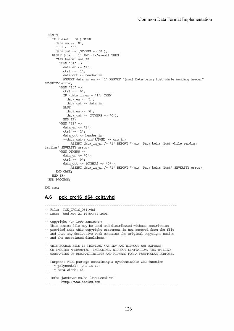
Common Data Format Implementation
126
BEGINIF (reset = '0') THENdata_en <= '0';ctrl <= '0';data_out <= (OTHERS => '0');
ELSIF (clk = '1' AND clk'event) THENCASE header_sel ISWHEN "01" =>data_en <= '1';ctrl <= '1';data_out <= header_in;ASSERT data_in_en /= '1' REPORT "(mux) Data being lost while sending header"
SEVERITY error;WHEN "10" =>ctrl <= '0';IF (data_in_en = '1') THENdata_en <= '1';data_out <= data_in;
ELSEdata_en <= '0';data_out <= (OTHERS => '0');
END IF;WHEN "11" =>data_en <= '1';ctrl <= '1';data_out <= header_in;--data_out(r_crc'RANGE) <= crc_in;
ASSERT data_in_en /= '1' REPORT "(mux) Data being lost while sendingtrailer" SEVERITY error;
WHEN OTHERS =>data_en <= '0';ctrl <= '0';data_out <= (OTHERS => '0');
ASSERT data_in_en /= '1' REPORT "(mux) Data being lost" SEVERITY error;END CASE;
END IF;END PROCESS;
END mux;
A.6 pck_crc16_d64_ccitt.vhd ------------------------------------------------------------------------- File: PCK_CRC16_D64.vhd-- Date: Wed Nov 21 16:54:49 2001---- Copyright (C) 1999 Easics NV.-- This source file may be used and distributed without restriction-- provided that this copyright statement is not removed from the file-- and that any derivative work contains the original copyright notice-- and the associated disclaimer.---- THIS SOURCE FILE IS PROVIDED "AS IS" AND WITHOUT ANY EXPRESS-- OR IMPLIED WARRANTIES, INCLUDING, WITHOUT LIMITATION, THE IMPLIED-- WARRANTIES OF MERCHANTIBILITY AND FITNESS FOR A PARTICULAR PURPOSE.---- Purpose: VHDL package containing a synthesizable CRC function-- * polynomial: (0 2 15 16)-- * data width: 64---- Info: [email protected] (Jan Decaluwe)-- http://www.easics.com-----------------------------------------------------------------------
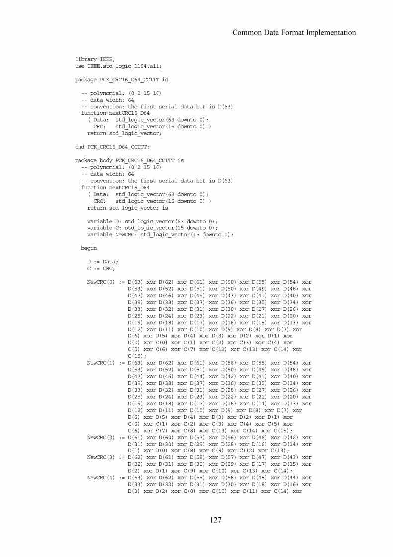
Common Data Format Implementation
127
library IEEE;use IEEE.std_logic_1164.all;
package PCK_CRC16_D64_CCITT is
-- polynomial: (0 2 15 16)-- data width: 64-- convention: the first serial data bit is D(63)function nextCRC16_D64( Data: std_logic_vector(63 downto 0);CRC: std_logic_vector(15 downto 0) )
return std_logic_vector;
end PCK_CRC16_D64_CCITT;
package body PCK_CRC16_D64_CCITT is-- polynomial: (0 2 15 16)-- data width: 64-- convention: the first serial data bit is D(63)function nextCRC16_D64( Data: std_logic_vector(63 downto 0);CRC: std_logic_vector(15 downto 0) )
return std_logic_vector is
variable D: std_logic_vector(63 downto 0);variable C: std_logic_vector(15 downto 0);variable NewCRC: std_logic_vector(15 downto 0);
begin
D := Data;C := CRC;
NewCRC(0) := D(63) xor D(62) xor D(61) xor D(60) xor D(55) xor D(54) xorD(53) xor D(52) xor D(51) xor D(50) xor D(49) xor D(48) xorD(47) xor D(46) xor D(45) xor D(43) xor D(41) xor D(40) xorD(39) xor D(38) xor D(37) xor D(36) xor D(35) xor D(34) xorD(33) xor D(32) xor D(31) xor D(30) xor D(27) xor D(26) xorD(25) xor D(24) xor D(23) xor D(22) xor D(21) xor D(20) xorD(19) xor D(18) xor D(17) xor D(16) xor D(15) xor D(13) xorD(12) xor D(11) xor D(10) xor D(9) xor D(8) xor D(7) xorD(6) xor D(5) xor D(4) xor D(3) xor D(2) xor D(1) xorD(0) xor C(0) xor C(1) xor C(2) xor C(3) xor C(4) xorC(5) xor C(6) xor C(7) xor C(12) xor C(13) xor C(14) xorC(15);
NewCRC(1) := D(63) xor D(62) xor D(61) xor D(56) xor D(55) xor D(54) xorD(53) xor D(52) xor D(51) xor D(50) xor D(49) xor D(48) xorD(47) xor D(46) xor D(44) xor D(42) xor D(41) xor D(40) xorD(39) xor D(38) xor D(37) xor D(36) xor D(35) xor D(34) xorD(33) xor D(32) xor D(31) xor D(28) xor D(27) xor D(26) xorD(25) xor D(24) xor D(23) xor D(22) xor D(21) xor D(20) xorD(19) xor D(18) xor D(17) xor D(16) xor D(14) xor D(13) xorD(12) xor D(11) xor D(10) xor D(9) xor D(8) xor D(7) xorD(6) xor D(5) xor D(4) xor D(3) xor D(2) xor D(1) xorC(0) xor C(1) xor C(2) xor C(3) xor C(4) xor C(5) xorC(6) xor C(7) xor C(8) xor C(13) xor C(14) xor C(15);
NewCRC(2) := D(61) xor D(60) xor D(57) xor D(56) xor D(46) xor D(42) xorD(31) xor D(30) xor D(29) xor D(28) xor D(16) xor D(14) xorD(1) xor D(0) xor C(8) xor C(9) xor C(12) xor C(13);
NewCRC(3) := D(62) xor D(61) xor D(58) xor D(57) xor D(47) xor D(43) xorD(32) xor D(31) xor D(30) xor D(29) xor D(17) xor D(15) xorD(2) xor D(1) xor C(9) xor C(10) xor C(13) xor C(14);
NewCRC(4) := D(63) xor D(62) xor D(59) xor D(58) xor D(48) xor D(44) xorD(33) xor D(32) xor D(31) xor D(30) xor D(18) xor D(16) xorD(3) xor D(2) xor C(0) xor C(10) xor C(11) xor C(14) xor
Common Data Format Implementation
128
C(15);NewCRC(5) := D(63) xor D(60) xor D(59) xor D(49) xor D(45) xor D(34) xor
D(33) xor D(32) xor D(31) xor D(19) xor D(17) xor D(4) xorD(3) xor C(1) xor C(11) xor C(12) xor C(15);
NewCRC(6) := D(61) xor D(60) xor D(50) xor D(46) xor D(35) xor D(34) xorD(33) xor D(32) xor D(20) xor D(18) xor D(5) xor D(4) xorC(2) xor C(12) xor C(13);
NewCRC(7) := D(62) xor D(61) xor D(51) xor D(47) xor D(36) xor D(35) xorD(34) xor D(33) xor D(21) xor D(19) xor D(6) xor D(5) xorC(3) xor C(13) xor C(14);
NewCRC(8) := D(63) xor D(62) xor D(52) xor D(48) xor D(37) xor D(36) xorD(35) xor D(34) xor D(22) xor D(20) xor D(7) xor D(6) xorC(0) xor C(4) xor C(14) xor C(15);
NewCRC(9) := D(63) xor D(53) xor D(49) xor D(38) xor D(37) xor D(36) xorD(35) xor D(23) xor D(21) xor D(8) xor D(7) xor C(1) xorC(5) xor C(15);
NewCRC(10) := D(54) xor D(50) xor D(39) xor D(38) xor D(37) xor D(36) xorD(24) xor D(22) xor D(9) xor D(8) xor C(2) xor C(6);
NewCRC(11) := D(55) xor D(51) xor D(40) xor D(39) xor D(38) xor D(37) xorD(25) xor D(23) xor D(10) xor D(9) xor C(3) xor C(7);
NewCRC(12) := D(56) xor D(52) xor D(41) xor D(40) xor D(39) xor D(38) xorD(26) xor D(24) xor D(11) xor D(10) xor C(4) xor C(8);
NewCRC(13) := D(57) xor D(53) xor D(42) xor D(41) xor D(40) xor D(39) xorD(27) xor D(25) xor D(12) xor D(11) xor C(5) xor C(9);
NewCRC(14) := D(58) xor D(54) xor D(43) xor D(42) xor D(41) xor D(40) xorD(28) xor D(26) xor D(13) xor D(12) xor C(6) xor C(10);
NewCRC(15) := D(63) xor D(62) xor D(61) xor D(60) xor D(59) xor D(54) xorD(53) xor D(52) xor D(51) xor D(50) xor D(49) xor D(48) xorD(47) xor D(46) xor D(45) xor D(44) xor D(42) xor D(40) xorD(39) xor D(38) xor D(37) xor D(36) xor D(35) xor D(34) xorD(33) xor D(32) xor D(31) xor D(30) xor D(29) xor D(26) xorD(25) xor D(24) xor D(23) xor D(22) xor D(21) xor D(20) xorD(19) xor D(18) xor D(17) xor D(16) xor D(15) xor D(14) xorD(12) xor D(11) xor D(10) xor D(9) xor D(8) xor D(7) xorD(6) xor D(5) xor D(4) xor D(3) xor D(2) xor D(1) xorD(0) xor C(0) xor C(1) xor C(2) xor C(3) xor C(4) xorC(5) xor C(6) xor C(11) xor C(12) xor C(13) xor C(14) xorC(15);
return NewCRC;
end nextCRC16_D64;
end PCK_CRC16_D64_CCITT;
A.7 pck_crc16_d64_x25.vhd ------------------------------------------------------------------------- File: PCK_CRC16_D64.vhd-- Date: Wed Nov 21 18:01:04 2001---- Copyright (C) 1999 Easics NV.-- This source file may be used and distributed without restriction-- provided that this copyright statement is not removed from the file-- and that any derivative work contains the original copyright notice-- and the associated disclaimer.---- THIS SOURCE FILE IS PROVIDED "AS IS" AND WITHOUT ANY EXPRESS-- OR IMPLIED WARRANTIES, INCLUDING, WITHOUT LIMITATION, THE IMPLIED-- WARRANTIES OF MERCHANTIBILITY AND FITNESS FOR A PARTICULAR PURPOSE.---- Purpose: VHDL package containing a synthesizable CRC function-- * polynomial: (0 5 12 16)
Common Data Format Implementation
129
-- * data width: 64---- Info: [email protected] (Jan Decaluwe)-- http://www.easics.com-----------------------------------------------------------------------
library IEEE;use IEEE.std_logic_1164.all;
package PCK_CRC16_D64_X25 is
-- polynomial: (0 5 12 16)-- data width: 64-- convention: the first serial data bit is D(63)function nextCRC16_D64( Data: std_logic_vector(63 downto 0);CRC: std_logic_vector(15 downto 0) )
return std_logic_vector;
end PCK_CRC16_D64_X25;
package body PCK_CRC16_D64_X25 is
-- polynomial: (0 5 12 16)-- data width: 64-- convention: the first serial data bit is D(63)function nextCRC16_D64( Data: std_logic_vector(63 downto 0);CRC: std_logic_vector(15 downto 0) )
return std_logic_vector is
variable D: std_logic_vector(63 downto 0);variable C: std_logic_vector(15 downto 0);variable NewCRC: std_logic_vector(15 downto 0);
begin
D := Data;C := CRC;
NewCRC(0) := D(63) xor D(58) xor D(56) xor D(55) xor D(52) xor D(51) xorD(49) xor D(48) xor D(42) xor D(35) xor D(33) xor D(32) xorD(28) xor D(27) xor D(26) xor D(22) xor D(20) xor D(19) xorD(12) xor D(11) xor D(8) xor D(4) xor D(0) xor C(0) xorC(1) xor C(3) xor C(4) xor C(7) xor C(8) xor C(10) xorC(15);
NewCRC(1) := D(59) xor D(57) xor D(56) xor D(53) xor D(52) xor D(50) xorD(49) xor D(43) xor D(36) xor D(34) xor D(33) xor D(29) xorD(28) xor D(27) xor D(23) xor D(21) xor D(20) xor D(13) xorD(12) xor D(9) xor D(5) xor D(1) xor C(1) xor C(2) xorC(4) xor C(5) xor C(8) xor C(9) xor C(11);
NewCRC(2) := D(60) xor D(58) xor D(57) xor D(54) xor D(53) xor D(51) xorD(50) xor D(44) xor D(37) xor D(35) xor D(34) xor D(30) xorD(29) xor D(28) xor D(24) xor D(22) xor D(21) xor D(14) xorD(13) xor D(10) xor D(6) xor D(2) xor C(2) xor C(3) xorC(5) xor C(6) xor C(9) xor C(10) xor C(12);
NewCRC(3) := D(61) xor D(59) xor D(58) xor D(55) xor D(54) xor D(52) xorD(51) xor D(45) xor D(38) xor D(36) xor D(35) xor D(31) xorD(30) xor D(29) xor D(25) xor D(23) xor D(22) xor D(15) xor

Common Data Format Implementation
130
D(14) xor D(11) xor D(7) xor D(3) xor C(3) xor C(4) xorC(6) xor C(7) xor C(10) xor C(11) xor C(13);
NewCRC(4) := D(62) xor D(60) xor D(59) xor D(56) xor D(55) xor D(53) xorD(52) xor D(46) xor D(39) xor D(37) xor D(36) xor D(32) xorD(31) xor D(30) xor D(26) xor D(24) xor D(23) xor D(16) xorD(15) xor D(12) xor D(8) xor D(4) xor C(4) xor C(5) xorC(7) xor C(8) xor C(11) xor C(12) xor C(14);
NewCRC(5) := D(61) xor D(60) xor D(58) xor D(57) xor D(55) xor D(54) xorD(53) xor D(52) xor D(51) xor D(49) xor D(48) xor D(47) xorD(42) xor D(40) xor D(38) xor D(37) xor D(35) xor D(31) xorD(28) xor D(26) xor D(25) xor D(24) xor D(22) xor D(20) xorD(19) xor D(17) xor D(16) xor D(13) xor D(12) xor D(11) xorD(9) xor D(8) xor D(5) xor D(4) xor D(0) xor C(0) xorC(1) xor C(3) xor C(4) xor C(5) xor C(6) xor C(7) xorC(9) xor C(10) xor C(12) xor C(13);
NewCRC(6) := D(62) xor D(61) xor D(59) xor D(58) xor D(56) xor D(55) xorD(54) xor D(53) xor D(52) xor D(50) xor D(49) xor D(48) xorD(43) xor D(41) xor D(39) xor D(38) xor D(36) xor D(32) xorD(29) xor D(27) xor D(26) xor D(25) xor D(23) xor D(21) xorD(20) xor D(18) xor D(17) xor D(14) xor D(13) xor D(12) xorD(10) xor D(9) xor D(6) xor D(5) xor D(1) xor C(0) xorC(1) xor C(2) xor C(4) xor C(5) xor C(6) xor C(7) xorC(8) xor C(10) xor C(11) xor C(13) xor C(14);
NewCRC(7) := D(63) xor D(62) xor D(60) xor D(59) xor D(57) xor D(56) xorD(55) xor D(54) xor D(53) xor D(51) xor D(50) xor D(49) xorD(44) xor D(42) xor D(40) xor D(39) xor D(37) xor D(33) xorD(30) xor D(28) xor D(27) xor D(26) xor D(24) xor D(22) xorD(21) xor D(19) xor D(18) xor D(15) xor D(14) xor D(13) xorD(11) xor D(10) xor D(7) xor D(6) xor D(2) xor C(1) xorC(2) xor C(3) xor C(5) xor C(6) xor C(7) xor C(8) xorC(9) xor C(11) xor C(12) xor C(14) xor C(15);
NewCRC(8) := D(63) xor D(61) xor D(60) xor D(58) xor D(57) xor D(56) xorD(55) xor D(54) xor D(52) xor D(51) xor D(50) xor D(45) xorD(43) xor D(41) xor D(40) xor D(38) xor D(34) xor D(31) xorD(29) xor D(28) xor D(27) xor D(25) xor D(23) xor D(22) xorD(20) xor D(19) xor D(16) xor D(15) xor D(14) xor D(12) xorD(11) xor D(8) xor D(7) xor D(3) xor C(2) xor C(3) xorC(4) xor C(6) xor C(7) xor C(8) xor C(9) xor C(10) xorC(12) xor C(13) xor C(15);
NewCRC(9) := D(62) xor D(61) xor D(59) xor D(58) xor D(57) xor D(56) xorD(55) xor D(53) xor D(52) xor D(51) xor D(46) xor D(44) xorD(42) xor D(41) xor D(39) xor D(35) xor D(32) xor D(30) xorD(29) xor D(28) xor D(26) xor D(24) xor D(23) xor D(21) xorD(20) xor D(17) xor D(16) xor D(15) xor D(13) xor D(12) xorD(9) xor D(8) xor D(4) xor C(3) xor C(4) xor C(5) xorC(7) xor C(8) xor C(9) xor C(10) xor C(11) xor C(13) xorC(14);
NewCRC(10) := D(63) xor D(62) xor D(60) xor D(59) xor D(58) xor D(57) xorD(56) xor D(54) xor D(53) xor D(52) xor D(47) xor D(45) xorD(43) xor D(42) xor D(40) xor D(36) xor D(33) xor D(31) xorD(30) xor D(29) xor D(27) xor D(25) xor D(24) xor D(22) xorD(21) xor D(18) xor D(17) xor D(16) xor D(14) xor D(13) xorD(10) xor D(9) xor D(5) xor C(4) xor C(5) xor C(6) xorC(8) xor C(9) xor C(10) xor C(11) xor C(12) xor C(14) xorC(15);
NewCRC(11) := D(63) xor D(61) xor D(60) xor D(59) xor D(58) xor D(57) xorD(55) xor D(54) xor D(53) xor D(48) xor D(46) xor D(44) xorD(43) xor D(41) xor D(37) xor D(34) xor D(32) xor D(31) xorD(30) xor D(28) xor D(26) xor D(25) xor D(23) xor D(22) xor
Common Data Format Implementation
131
D(19) xor D(18) xor D(17) xor D(15) xor D(14) xor D(11) xorD(10) xor D(6) xor C(0) xor C(5) xor C(6) xor C(7) xorC(9) xor C(10) xor C(11) xor C(12) xor C(13) xor C(15);
NewCRC(12) := D(63) xor D(62) xor D(61) xor D(60) xor D(59) xor D(54) xorD(52) xor D(51) xor D(48) xor D(47) xor D(45) xor D(44) xorD(38) xor D(31) xor D(29) xor D(28) xor D(24) xor D(23) xorD(22) xor D(18) xor D(16) xor D(15) xor D(8) xor D(7) xorD(4) xor D(0) xor C(0) xor C(3) xor C(4) xor C(6) xorC(11) xor C(12) xor C(13) xor C(14) xor C(15);
NewCRC(13) := D(63) xor D(62) xor D(61) xor D(60) xor D(55) xor D(53) xorD(52) xor D(49) xor D(48) xor D(46) xor D(45) xor D(39) xorD(32) xor D(30) xor D(29) xor D(25) xor D(24) xor D(23) xorD(19) xor D(17) xor D(16) xor D(9) xor D(8) xor D(5) xorD(1) xor C(0) xor C(1) xor C(4) xor C(5) xor C(7) xorC(12) xor C(13) xor C(14) xor C(15);
NewCRC(14) := D(63) xor D(62) xor D(61) xor D(56) xor D(54) xor D(53) xorD(50) xor D(49) xor D(47) xor D(46) xor D(40) xor D(33) xorD(31) xor D(30) xor D(26) xor D(25) xor D(24) xor D(20) xorD(18) xor D(17) xor D(10) xor D(9) xor D(6) xor D(2) xorC(1) xor C(2) xor C(5) xor C(6) xor C(8) xor C(13) xorC(14) xor C(15);
NewCRC(15) := D(63) xor D(62) xor D(57) xor D(55) xor D(54) xor D(51) xorD(50) xor D(48) xor D(47) xor D(41) xor D(34) xor D(32) xorD(31) xor D(27) xor D(26) xor D(25) xor D(21) xor D(19) xorD(18) xor D(11) xor D(10) xor D(7) xor D(3) xor C(0) xorC(2) xor C(3) xor C(6) xor C(7) xor C(9) xor C(14) xorC(15);
return NewCRC;
end nextCRC16_D64;
end PCK_CRC16_D64_X25;
132
Appendix B: Common Data Format Verification Code The verification code for the common data format block includes a testbench,
written in VHDL, and a program written in C that analyses the output of the testbench.
The testbench includes a top-level block diagram that connects the test code to the
device under test (DUT), and the test code itself. For the block diagram, the generated
VHDL is listed (testbench.vhd). The test code (tester.vhd) sends test data to the DUT,
and then writes the output signals to a text file. The VHDL code was developed with
HDL Designer, and run in ModelSim, both part of Mentor Graphics FPGA Advantage.
The C code reads the text file generated by the test-bench, and verifies its
correctness. It includes a reference CRC algorithm (crcmodel.h and crcmodel.c, adapted
from ref [43]) to calculate the CRC of the data and compare it to the VHDL-generated
value. It was developed with Microsoft Visual C++.
B.1 testbench.vhd -- hds header_start---- VHDL Entity FED_DATA_FORMAT.data_format_tb.symbol---- Created:-- by - corrinep.UNKNOWN (EMLYN)-- at - 10:58:41 10/26/02---- Generated by Mentor Graphics' HDL Designer(TM) 2002.1a (Build 22)---- hds header_end
ENTITY data_format_tb IS-- Declarations
END data_format_tb ;
-- hds interface_end---- VHDL Architecture FED_DATA_FORMAT.data_format_tb.testbench---- Created:-- by - corrinep.UNKNOWN (EMLYN)-- at - 10:58:42 10/26/02---- Generated by Mentor Graphics' HDL Designer(TM) 2002.1a (Build 22)--LIBRARY ieee;USE ieee.std_logic_1164.all;USE ieee.std_logic_arith.all;
Common Data Format Verification Code
133
LIBRARY FED_DATA_FORMAT;
ARCHITECTURE testbench OF data_format_tb IS
-- Architecture declarations
-- Internal signal declarationsSIGNAL clk : std_logic;SIGNAL ctrl : std_logic;SIGNAL data_bx_id : std_logic_vector(11 DOWNTO 0);SIGNAL data_evt_lgth : std_logic_vector(23 DOWNTO 0);SIGNAL data_evt_stat : std_logic_vector(7 DOWNTO 0);SIGNAL data_evt_ty : std_logic_vector(3 DOWNTO 0);SIGNAL data_in : std_logic_vector(63 DOWNTO 0);SIGNAL data_in_en : std_logic;SIGNAL data_lv1_id : std_logic_vector(23 DOWNTO 0);SIGNAL data_out : std_logic_vector(63 DOWNTO 0);SIGNAL data_out_en : std_logic;SIGNAL data_source_id : std_logic_vector(11 DOWNTO 0);SIGNAL linkfull : std_logic;SIGNAL rd_ready : std_logic;SIGNAL rd_start : std_logic;SIGNAL rd_stop : std_logic;SIGNAL reset : std_logic;SIGNAL wr_ready : std_logic;SIGNAL wr_start : std_logic;
-- Component DeclarationsCOMPONENT data_formatGENERIC (
fifo_addr_bits : natural := 9;length_at_start : boolean := true
);PORT (
clk : IN std_logic ;data_bx_id : IN std_logic_vector (11 DOWNTO 0);data_evt_lgth : IN std_logic_vector (23 DOWNTO 0);data_evt_stat : IN std_logic_vector (7 DOWNTO 0);data_evt_ty : IN std_logic_vector (3 DOWNTO 0);data_in : IN std_logic_vector (63 DOWNTO 0);data_in_en : IN std_logic ;data_lv1_id : IN std_logic_vector (23 DOWNTO 0);data_source_id : IN std_logic_vector (11 DOWNTO 0);linkfull : IN std_logic ;rd_start : IN std_logic ;rd_stop : IN std_logic ;reset : IN std_logic ;wr_start : IN std_logic ;ctrl : OUT std_logic ;data_out : OUT std_logic_vector (63 DOWNTO 0);data_out_en : OUT std_logic ;rd_ready : OUT std_logic ;wr_ready : OUT std_logic
);END COMPONENT;COMPONENT data_format_testerPORT (
ctrl : IN std_logic ;data_out : IN std_logic_vector (63 DOWNTO 0);

Common Data Format Verification Code
134
data_out_en : IN std_logic ;rd_ready : IN std_logic ;wr_ready : IN std_logic ;clk : OUT std_logic ;data_bx_id : OUT std_logic_vector (11 DOWNTO 0);data_evt_lgth : OUT std_logic_vector (23 DOWNTO 0);data_evt_stat : OUT std_logic_vector (7 DOWNTO 0);data_evt_ty : OUT std_logic_vector (3 DOWNTO 0);data_in : OUT std_logic_vector (63 DOWNTO 0);data_in_en : OUT std_logic ;data_lv1_id : OUT std_logic_vector (23 DOWNTO 0);data_source_id : OUT std_logic_vector (11 DOWNTO 0);linkfull : OUT std_logic ;rd_start : OUT std_logic ;rd_stop : OUT std_logic ;reset : OUT std_logic ;wr_start : OUT std_logic
);END COMPONENT;
-- Optional embedded configurations-- pragma synthesis_offFOR ALL : data_format USE ENTITY FED_DATA_FORMAT.data_format;FOR ALL : data_format_tester USE ENTITY FED_DATA_FORMAT.data_format_tester;-- pragma synthesis_on
BEGIN-- Instance port mappings.I0 : data_format
GENERIC MAP (fifo_addr_bits => 9,length_at_start => true
)PORT MAP (
clk => clk,data_bx_id => data_bx_id,data_evt_lgth => data_evt_lgth,data_evt_stat => data_evt_stat,data_evt_ty => data_evt_ty,data_in => data_in,data_in_en => data_in_en,data_lv1_id => data_lv1_id,data_source_id => data_source_id,linkfull => linkfull,rd_start => rd_start,rd_stop => rd_stop,reset => reset,wr_start => wr_start,ctrl => ctrl,data_out => data_out,data_out_en => data_out_en,rd_ready => rd_ready,wr_ready => wr_ready
);I1 : data_format_tester
PORT MAP (ctrl => ctrl,data_out => data_out,data_out_en => data_out_en,
Common Data Format Verification Code
135
rd_ready => rd_ready,wr_ready => wr_ready,clk => clk,data_bx_id => data_bx_id,data_evt_lgth => data_evt_lgth,data_evt_stat => data_evt_stat,data_evt_ty => data_evt_ty,data_in => data_in,data_in_en => data_in_en,data_lv1_id => data_lv1_id,data_source_id => data_source_id,linkfull => linkfull,rd_start => rd_start,rd_stop => rd_stop,reset => reset,wr_start => wr_start
);END testbench;
B.2 tester.vhd -- hds header_start---- VHDL Architecture FED_DATA_FORMAT.data_format_tester.untitled---- Created:-- by - corrinep.UNKNOWN (EMLYN)-- at - 15:59:19 10/03/02---- Generated by Mentor Graphics' HDL Designer(TM) 2002.1a (Build 22)---- hds header_endLIBRARY ieee;USE ieee.std_logic_1164.all;USE ieee.std_logic_arith.all;
ENTITY data_format_tester ISPORT(
ctrl : IN std_logic;data_out : IN std_logic_vector (63 DOWNTO 0);data_out_en : IN std_logic;rd_ready : IN std_logic;wr_ready : IN std_logic;clk : OUT std_logic;data_bx_id : OUT std_logic_vector (11 DOWNTO 0);data_evt_lgth : OUT std_logic_vector (23 DOWNTO 0);data_evt_stat : OUT std_logic_vector (7 DOWNTO 0);data_evt_ty : OUT std_logic_vector (3 DOWNTO 0);data_in : OUT std_logic_vector (63 DOWNTO 0);data_in_en : OUT std_logic;data_lv1_id : OUT std_logic_vector (23 DOWNTO 0);data_source_id : OUT std_logic_vector (11 DOWNTO 0);linkfull : OUT std_logic;rd_start : OUT std_logic;rd_stop : OUT std_logic;reset : OUT std_logic;wr_start : OUT std_logic
);

Common Data Format Verification Code
136
-- Declarations
END data_format_tester ;
-- hds interface_end
USE std.textio.ALL;
LIBRARY ieee;USE ieee.std_logic_arith.ALL;USE ieee.std_logic_unsigned.ALL;
LIBRARY FED_DATA_FORMAT;USE FED_DATA_FORMAT.RNG.ALL;
ARCHITECTURE tester OF data_format_tester IS
FUNCTION chr(sl: std_logic) RETURN character isVARIABLE c: character;
BEGINCASE sl ISWHEN 'U' => c:= 'U';WHEN 'X' => c:= 'X';WHEN '0' => c:= '0';WHEN '1' => c:= '1';WHEN 'Z' => c:= 'Z';WHEN 'W' => c:= 'W';WHEN 'L' => c:= 'L';WHEN 'H' => c:= 'H';WHEN '-' => c:= '-';WHEN OTHERS => c := '?';
END CASE;RETURN c;
END chr;
FUNCTION str(sl: std_logic) RETURN string ISVARIABLE s: string(1 TO 1);
BEGINs(1) := chr(sl);RETURN s;
END str;
FUNCTION str(slv: std_logic_vector) RETURN string ISVARIABLE s: string(1 TO slv'length);VARIABLE i, j: integer;
BEGINj := 1;FOR i IN slv'RANGE LOOPs(j) := chr(slv(i));j := j + 1;
END LOOP;RETURN s;
END str;
PROCEDURE RndSlv(rng: INOUT random; ret: OUT std_logic_vector) ISVARIABLE r: std_logic_vector(63 DOWNTO 0);
BEGINGenRnd(rng);r(63 DOWNTO 48) := conv_std_logic_vector(integer(rng.rnd), 16);
Common Data Format Verification Code
137
GenRnd(rng);r(47 DOWNTO 32) := conv_std_logic_vector(integer(rng.rnd), 16);GenRnd(rng);r(31 DOWNTO 16) := conv_std_logic_vector(integer(rng.rnd), 16);GenRnd(rng);r(15 DOWNTO 0) := conv_std_logic_vector(integer(rng.rnd), 16);ret := r;
END RndSlv;
CONSTANT half_period: time := 12500 ps;TYPE state_type IS (idle, pause, data);TYPE arr IS ARRAY(NATURAL RANGE<>) OF NATURAL;CONSTANT lengths: arr := (24, 10, 15, 0, 70, 1);FILE output: text IS OUT "tester.txt";SIGNAL clk_int, trigger: std_logic;
BEGIN
clk <= clk_int;
clock: process(clk_int)VARIABLE started: boolean := FALSE;
BEGINIF (NOT STARTED) THENclk_int <= '1';STARTED := TRUE;
ELSIF (clk_int = '0' AND clk_int'event) THENclk_int <= '1' AFTER half_period;
ELSIF (clk_int = '1' AND clk_int'event) THENclk_int <= '0' AFTER half_period;
END IF;END PROCESS;
tester: PROCESS(clk_int)VARIABLE count_bx_id, count_lv1_id, count_trig, count_read, read_length,
count_pause : natural;VARIABLE done_reset: boolean := false;VARIABLE state: state_type;VARIABLE data_in_tmp: std_logic_vector(63 DOWNTO 0);VARIABLE rng: random := CvtRandom(InitUniform(9876, 0.0, 65536.0));VARIABLE buf: line;
BEGINIF (clk_int = '1' AND clk_int'event) THEN-- default assignmentsdata_in <= (OTHERS => 'Z');data_bx_id <= (OTHERS => 'Z');data_evt_lgth <= (OTHERS => 'Z');data_evt_stat <= (OTHERS => 'Z');data_evt_ty <= (OTHERS => 'Z');data_lv1_id <= (OTHERS => 'Z');data_source_id <= (OTHERS => 'Z');data_in_en <= '0';wr_start <= '0';rd_start <= '0';rd_stop <= '0';linkfull <= '0';reset <= '1';trigger <= '0';

Common Data Format Verification Code
138
IF (NOT done_reset) THENwrite(buf, string'("Start of run"));writeline(output, buf);state := idle;reset <= '0';count_trig := 0;count_bx_id := 0;count_lv1_id := 0;count_read := 0;done_reset := true;
END IF;
CASE count_bx_id IS
WHEN 6 | 45 | 47 | 92 | 119 =>count_trig := count_trig + 1;trigger <= '1';
WHEN 120 TO 160 =>linkfull <= '1';
WHEN 250 =>writeline(output, buf);write(buf, string'("End of run"));writeline(output, buf);ASSERT false REPORT "End of test run" SEVERITY failure;
WHEN OTHERS =>-- do nothing
END CASE;
IF (count_trig > 0 AND wr_ready = '1') THENcount_trig := count_trig - 1;count_lv1_id := count_lv1_id + 1;data_evt_ty <= (OTHERS => '1');data_lv1_id <= std_logic_vector(conv_unsigned(count_lv1_id,
data_lv1_id'length));data_bx_id <= std_logic_vector(conv_unsigned(count_bx_id,
data_bx_id'length));data_source_id <= "101100111000";data_evt_ty <= (OTHERS => '1');data_evt_lgth <= conv_std_logic_vector(lengths(count_lv1_id-1),
data_evt_lgth'length);data_evt_stat <= (OTHERS => '0');wr_start <= '1';
END IF;
IF (data_out_en = '1') THENwrite(buf, str(ctrl));write(buf, string'(" "));write(buf, str(data_out));writeline(output, buf);
END IF;
CASE state ISWHEN idle =>IF (rd_ready = '1') THENrd_start <= '1';read_length := lengths(count_read);
Common Data Format Verification Code
139
count_read := count_read + 1;writeline(output, buf);write(buf, string'("Event "));write(buf, count_read);write(buf, string'(" at "));write(buf, count_bx_id);writeline(output, buf);count_pause := 3;state := pause;
END IF;
WHEN pause =>count_pause := count_pause - 1;IF (count_pause <= 0) THENstate := data;
END IF;
WHEN data =>IF (read_length > 0) THENIF (wr_ready = '1') THENRndSlv(rng, data_in_tmp);data_in <= data_in_tmp;data_in_en <= '1';read_length := read_length - 1;
END IF;ELSErd_stop <= '1';state := idle;
END IF;END CASE;
count_bx_id := count_bx_id + 1;END IF;
END PROCESS;
END tester;
B.3 main.c #include <stdlib.h>#include <stdio.h>#include <string.h>
#include "crcmodel.h"
void crc64(p_cm_t, char*);ulong getnum(char*, int);
const ulong POLY_CCITT = 0x8005;const ulong POLY_X25 = 0x1021;
int main(void) const char *infile = "tester.txt";unsigned long num = 0;char buf[256];int state = 0;FILE *in;
cm_t crc;
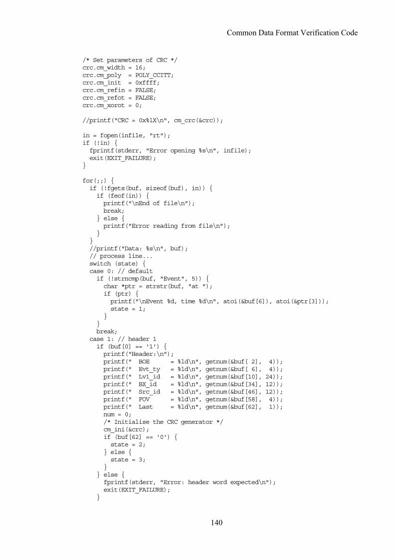
Common Data Format Verification Code
140
/* Set parameters of CRC */crc.cm_width = 16;crc.cm_poly = POLY_CCITT;crc.cm_init = 0xffff;crc.cm_refin = FALSE;crc.cm_refot = FALSE;crc.cm_xorot = 0;
//printf("CRC = 0x%lX\n", cm_crc(&crc));
in = fopen(infile, "rt");if (!in) fprintf(stderr, "Error opening %s\n", infile);exit(EXIT_FAILURE);
for(;;) if (!fgets(buf, sizeof(buf), in)) if (feof(in)) printf("\nEnd of file\n");break;
else printf("Error reading from file\n");
//printf("Data: %s\n", buf);// process line...switch (state) case 0: // defaultif (!strncmp(buf, "Event", 5)) char *ptr = strstr(buf, "at ");if (ptr) printf("\nEvent %d, time %d\n", atoi(&buf[6]), atoi(&ptr[3]));state = 1;
break;
case 1: // header 1if (buf[0] == '1') printf("Header:\n");printf(" BOE = %ld\n", getnum(&buf[ 2], 4));printf(" Evt_ty = %ld\n", getnum(&buf[ 6], 4));printf(" Lv1_id = %ld\n", getnum(&buf[10], 24));printf(" BX_id = %ld\n", getnum(&buf[34], 12));printf(" Src_id = %ld\n", getnum(&buf[46], 12));printf(" FOV = %ld\n", getnum(&buf[58], 4));printf(" Last = %ld\n", getnum(&buf[62], 1));num = 0;/* Initialise the CRC generator */cm_ini(&crc);if (buf[62] == '0') state = 2;
else state = 3;
else fprintf(stderr, "Error: header word expected\n");exit(EXIT_FAILURE);
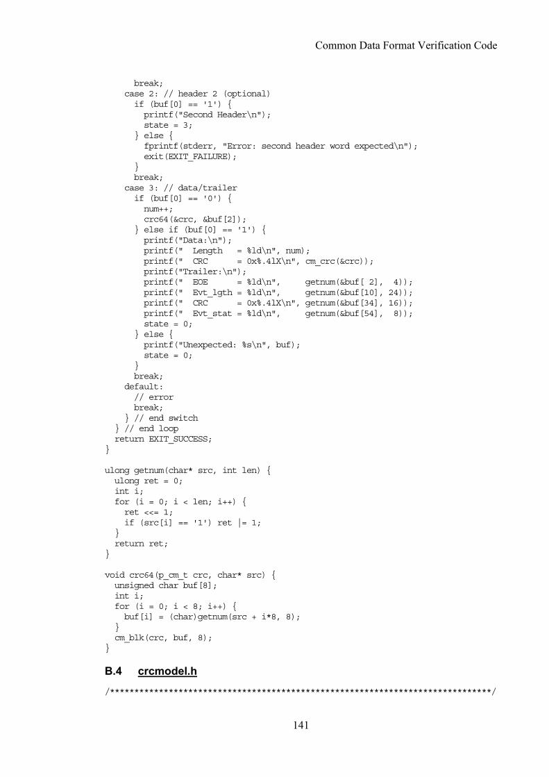
Common Data Format Verification Code
141
break;case 2: // header 2 (optional)if (buf[0] == '1') printf("Second Header\n");state = 3;
else fprintf(stderr, "Error: second header word expected\n");exit(EXIT_FAILURE);
break;
case 3: // data/trailerif (buf[0] == '0') num++;crc64(&crc, &buf[2]);
else if (buf[0] == '1') printf("Data:\n");printf(" Length = %ld\n", num);printf(" CRC = 0x%.4lX\n", cm_crc(&crc));printf("Trailer:\n");printf(" EOE = %ld\n", getnum(&buf[ 2], 4));printf(" Evt_lgth = %ld\n", getnum(&buf[10], 24));printf(" CRC = 0x%.4lX\n", getnum(&buf[34], 16));printf(" Evt_stat = %ld\n", getnum(&buf[54], 8));state = 0;
else printf("Unexpected: %s\n", buf);state = 0;
break;
default:// errorbreak;
// end switch // end loopreturn EXIT_SUCCESS;
ulong getnum(char* src, int len) ulong ret = 0;int i;for (i = 0; i < len; i++) ret <<= 1;if (src[i] == '1') ret |= 1;
return ret;
void crc64(p_cm_t crc, char* src) unsigned char buf[8];int i;for (i = 0; i < 8; i++) buf[i] = (char)getnum(src + i*8, 8);
cm_blk(crc, buf, 8);
B.4 crcmodel.h /******************************************************************************/

Common Data Format Verification Code
142
/* Start of crcmodel.h *//******************************************************************************//* *//* Author : Ross Williams ([email protected].). *//* Date : 3 June 1993. *//* Status : Public domain. *//* *//* Description : This is the header (.h) file for the reference *//* implementation of the Rocksoft^tm Model CRC Algorithm. For more *//* information on the Rocksoft^tm Model CRC Algorithm, see the document *//* titled "A Painless Guide to CRC Error Detection Algorithms" by Ross *//* Williams ([email protected].). This document is likely to be in *//* "ftp.adelaide.edu.au/pub/rocksoft". *//* *//* Note: Rocksoft is a trademark of Rocksoft Pty Ltd, Adelaide, Australia. *//* *//******************************************************************************//* *//* How to Use This Package *//* ----------------------- *//* Step 1: Declare a variable of type cm_t. Declare another variable *//* (p_cm say) of type p_cm_t and initialize it to point to the first *//* variable (e.g. p_cm_t p_cm = &cm_t). *//* *//* Step 2: Assign values to the parameter fields of the structure. *//* If you don't know what to assign, see the document cited earlier. *//* For example: *//* p_cm->cm_width = 16; *//* p_cm->cm_poly = 0x8005L; *//* p_cm->cm_init = 0L; *//* p_cm->cm_refin = TRUE; *//* p_cm->cm_refot = TRUE; *//* p_cm->cm_xorot = 0L; *//* Note: Poly is specified without its top bit (18005 becomes 8005). *//* Note: Width is one bit less than the raw poly width. *//* *//* Step 3: Initialize the instance with a call cm_ini(p_cm); *//* *//* Step 4: Process zero or more message bytes by placing zero or more *//* successive calls to cm_nxt. Example: cm_nxt(p_cm,ch); *//* *//* Step 5: Extract the CRC value at any time by calling crc = cm_crc(p_cm); *//* If the CRC is a 16-bit value, it will be in the bottom 16 bits. *//* *//******************************************************************************//* *//* Design Notes *//* ------------ *//* PORTABILITY: This package has been coded very conservatively so that *//* it will run on as many machines as possible. For example, all external *//* identifiers have been restricted to 6 characters and all internal ones to *//* 8 characters. The prefix cm (for Crc Model) is used as an attempt to avoid *//* namespace collisions. This package is endian independent. *//* *//* EFFICIENCY: This package (and its interface) is not designed for *//* speed. The purpose of this package is to act as a well-defined reference *//* model for the specification of CRC algorithms. If you want speed, cook up *//* a specific table-driven implementation as described in the document cited *//* above. This package is designed for validation only; if you have found or */
Common Data Format Verification Code
143
/* implemented a CRC algorithm and wish to describe it as a set of parameters *//* to the Rocksoft^tm Model CRC Algorithm, your CRC algorithm implementation *//* should behave identically to this package under those parameters. *//* *//******************************************************************************/
/* The following #ifndef encloses this entire *//* header file, rendering it indempotent. */#ifndef CM_DONE#define CM_DONE
/******************************************************************************/
/* The following definitions are extracted from my style header file which *//* would be cumbersome to distribute with this package. The DONE_STYLE is the *//* idempotence symbol used in my style header file. */
#ifndef DONE_STYLE
typedef unsigned long ulong;typedef unsigned bool;typedef unsigned char * p_ubyte_;
#ifndef TRUE#define FALSE 0#define TRUE 1#endif
#endif
/******************************************************************************/
/* CRC Model Abstract Type *//* ----------------------- *//* The following type stores the context of an executing instance of the *//* model algorithm. Most of the fields are model parameters which must be *//* set before the first initializing call to cm_ini. */typedef structint cm_width; /* Parameter: Width in bits [8,32]. */ulong cm_poly; /* Parameter: The algorithm's polynomial. */ulong cm_init; /* Parameter: Initial register value. */bool cm_refin; /* Parameter: Reflect input bytes? */bool cm_refot; /* Parameter: Reflect output CRC? */ulong cm_xorot; /* Parameter: XOR this to output CRC. */
ulong cm_reg; /* Context: Context during execution. */ cm_t;
typedef cm_t *p_cm_t;
/******************************************************************************/
/* Functions That Implement The Model *//* ---------------------------------- *//* The following functions animate the cm_t abstraction. */
void cm_ini(p_cm_t p_cm);/* Initializes the argument CRC model instance. *//* All parameter fields must be set before calling this. */
Common Data Format Verification Code
144
void cm_nxt(p_cm_t p_cm,int ch);/* Processes a single message byte [0,255]. */
void cm_blk(p_cm_t p_cm,p_ubyte_ blk_adr,ulong blk_len);/* Processes a block of message bytes. */
ulong cm_crc(p_cm_t p_cm);/* Returns the CRC value for the message bytes processed so far. */
/******************************************************************************/
/* Functions For Table Calculation *//* ------------------------------- *//* The following function can be used to calculate a CRC lookup table. *//* It can also be used at run-time to create or check static tables. */
ulong cm_tab(p_cm_t p_cm,int index);/* Returns the i'th entry for the lookup table for the specified algorithm. *//* The function examines the fields cm_width, cm_poly, cm_refin, and the *//* argument table index in the range [0,255] and returns the table entry in *//* the bottom cm_width bytes of the return value. */
/******************************************************************************/
/* End of the header file idempotence #ifndef */#endif
/******************************************************************************//* End of crcmodel.h *//******************************************************************************/
B.5 crcmodel.c /******************************************************************************//* Start of crcmodel.c *//******************************************************************************//* *//* Author : Ross Williams ([email protected].). *//* Date : 3 June 1993. *//* Status : Public domain. *//* *//* Description : This is the implementation (.c) file for the reference *//* implementation of the Rocksoft^tm Model CRC Algorithm. For more *//* information on the Rocksoft^tm Model CRC Algorithm, see the document *//* titled "A Painless Guide to CRC Error Detection Algorithms" by Ross *//* Williams ([email protected].). This document is likely to be in *//* "ftp.adelaide.edu.au/pub/rocksoft". *//* *//* Note: Rocksoft is a trademark of Rocksoft Pty Ltd, Adelaide, Australia. *//* *//******************************************************************************//* *//* Implementation Notes *//* -------------------- *//* To avoid inconsistencies, the specification of each function is not echoed *//* here. See the header file for a description of these functions. *//* This package is light on checking because I want to keep it short and */
Common Data Format Verification Code
145
/* simple and portable (i.e. it would be too messy to distribute my entire *//* C culture (e.g. assertions package) with this package. *//* *//******************************************************************************/
#include "crcmodel.h"
/******************************************************************************/
/* The following definitions make the code more readable. */
#define BITMASK(X) (1L << (X))#define MASK32 0xFFFFFFFFL#define LOCAL static
/******************************************************************************/
static ulong reflect(ulong v, int b) /* Returns the value v with the bottom b [0,32] bits reflected. *//* Example: reflect(0x3e23L,3) == 0x3e26 */int i;ulong t = v;for (i=0; i<b; i++) if (t & 1L) v|= BITMASK((b-1)-i);
else v&= ~BITMASK((b-1)-i);
t>>=1;
return v;
/******************************************************************************/
static ulong widmask(p_cm_t p_cm)/* Returns a longword whose value is (2^p_cm->cm_width)-1. *//* The trick is to do this portably (e.g. without doing <<32). */return (((1L<<(p_cm->cm_width-1))-1L)<<1)|1L;
/******************************************************************************/
void cm_ini(p_cm_t p_cm) p_cm->cm_reg = p_cm->cm_init;
/******************************************************************************/
void cm_nxt(p_cm_t p_cm, int ch) int i;ulong uch = (ulong) ch;ulong topbit = BITMASK(p_cm->cm_width-1);
if (p_cm->cm_refin) uch = reflect(uch,8);p_cm->cm_reg ^= (uch << (p_cm->cm_width-8));for (i=0; i<8; i++) if (p_cm->cm_reg & topbit)
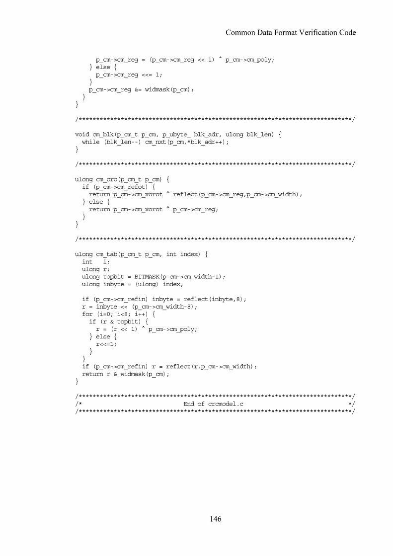
Common Data Format Verification Code
146
p_cm->cm_reg = (p_cm->cm_reg << 1) ^ p_cm->cm_poly; else p_cm->cm_reg <<= 1;
p_cm->cm_reg &= widmask(p_cm);
/******************************************************************************/
void cm_blk(p_cm_t p_cm, p_ubyte_ blk_adr, ulong blk_len) while (blk_len--) cm_nxt(p_cm,*blk_adr++);
/******************************************************************************/
ulong cm_crc(p_cm_t p_cm) if (p_cm->cm_refot) return p_cm->cm_xorot ^ reflect(p_cm->cm_reg,p_cm->cm_width);
else return p_cm->cm_xorot ^ p_cm->cm_reg;
/******************************************************************************/
ulong cm_tab(p_cm_t p_cm, int index) int i;ulong r;ulong topbit = BITMASK(p_cm->cm_width-1);ulong inbyte = (ulong) index;
if (p_cm->cm_refin) inbyte = reflect(inbyte,8);r = inbyte << (p_cm->cm_width-8);for (i=0; i<8; i++) if (r & topbit) r = (r << 1) ^ p_cm->cm_poly;
else r<<=1;
if (p_cm->cm_refin) r = reflect(r,p_cm->cm_width);return r & widmask(p_cm);
/******************************************************************************//* End of crcmodel.c *//******************************************************************************/
147
References 1. ALEPH DELPHI L3 and OPAL Collaborations (2002). Search for the Standard
Model Higgs Boson at LEP. ICHEP'02 (Amsterdam, July 2002) . http://lephiggs.web.cern.ch/LEPHIGGS/papers/July2002_SM/index.html
2. ALEPH DELPHI L3 and OPAL Collaborations (2002). Search for the Standard Model Higgs Boson at LEP. ICHEP'02 (Amsterdam, July 2002) .
http://lephiggs.web.cern.ch/LEPHIGGS/papers/July2002_SM/index.html
3. Denegri D. et al. (1994). B Physics and CP Violation Studies with the CMS Detector at LHC. Int. J. Mod. Phys. A 9, 4211-4255.
4. CMS Collaboration (1994). The Compact Muon Solenoid Technical Proposal. (CERN/LHCC 94-38).
5. CMS Collaboration (1997). CMS: The Magnet Project - Technical Design Report. (CERN/LHCC 97-010).
6. CMS Collaboration (1998). CMS Tracker Project Technical Design Report. (CERN/LHCC 98-6).
7. CMS Collaboration (2000). Addendum to the CMS Tracker TDR. (CERN/LHCC 2000-016).
8. CMS Collaboration (1997). CMS Electromagnetic Calorimeter Technical Design Report. (CERN/LHCC 97-33).
9. CMS Collaboration (1997). CMS Hadron Calorimeter Project Technical Design Report. (CERN/LHCC 97-32).
10. CMS Collaboration (1997). CMS Muon System Technical Design Report. (CERN/LHCC 97-32).
11. Wultz C.-E. (2001). Concept of the First Level Global Trigger for the CMS experiment at LHC. Nucl. Instrum. Meth. A473 (3), 231-242.
12. Brown S. & Rose J. (1996). Architecture of FPGAs and CPLDs: A Tutorial. IEEE Design and Test of Computers 13 (2), 42-57.
http://www.eecg.toronto.edu/~jayar/pubs/brown/survey.ps.gz
13. McCalmont S. (2002). EE465 - Digital IC Design. (Iowa State University, Course Notes).
http://class.ee.iastate.edu/ee465/
14. Smith M.J.S. (1997). Application Specific Integrated Circuits. (Addison-Wesley).

References
148
15. Cheung P.Y.K. (2002). Digital System Design. (Imperial College London Department of Electrical and Electronic Engineering, Course Notes).
http://www.ee.ic.ac.uk/pcheung/teaching/ee3_DSD/
16. Virtex-II 1.5V Platform FPGAs Data Sheet (2002). Summary of Virtex-II Features. (Xilinx).
http://www.xilinx.com/partinfo/ds031-1.pdf
17. Virtex-II 1.5V Platform FPGAs Data Sheet (2001). Detailed Description. (Xilinx).
http://www.xilinx.com/partinfo/ds031-2.pdf
18. Smith D.J. (2002). VHDL & Verilog Compared & Contrasted. (Veribest Inc.). http://www.angelfire.com/in/rajesh52/verilogvhdl.html
19. A Designer's Guide to Verilog (2002). (Doulos). http://www.doulos.com/fi/dgvlog_fr.html
20. A Designer's Guide to VHDL (2002). (Doulos). http://www.doulos.com/fi/dgvhdl_fr.html
21. Thacker E. (2001). System Ace: Configuration Solution for Xilinx FPGAs. (White Paper, Version 1.0). (Xilinx Inc.).
http://www.xilinx.com/publications/whitepapers/wp_pdf/wp151.pdf
22. Hall G. (1992). Modern charged particle detectors. Contemporary Physics 33 (1), 1-14.
23. Jones L. (2001). APV25S1 Design Overview. http://www.te.rl.ac.uk/INS/Electronic_Systems/Microelectronics_Design/Projects/
High_Energy_Physics/CMS/APV25-S1/files/Overview.pdf
24. Fulcher J.R. (2001). Radiation Effects in Electronics for the CMS Tracking Detector. (Imperial College).
25. Jones L. (2001). APV25-S1 User Guide. (Version 2.2). http://www.te.rl.ac.uk/med/projects/High_Energy_Physics/CMS/APV25-
S1/pdf/User_Guide_2.2.pdf
26. Jones L.L. et al. (1999). The APV25 Deep Submicron Readout Chip for CMS Detectors. 5th Workshop on Electronics for LHC Experiments, Snowmass, Colorado.
27. Hall G. (2000). The Deconvolution Method of Pulse Shaping.
28. The I2C Bus Specification (2000). (Version 2.1). (Philips). http://www.semiconductors.philips.com/buses/i2c/
29. Murray P. (2000). APVMUX User Guide. (Version 1.0).

References
149
30. CMS Tracker Optical Readout Link Specification (2001). Part 2: Analogue opto-hybrid. (Version 3.2).
31. Coughlan J.A. et al. (2002). The Front-End Driver Card for the CMS Silicon Strip Tracker Readout. 8th Workshop on Electronics for LHC Experiments, Colmar, France.
32. Racz A. et al. (2002). CMS data to surface transportation architecture. (8th Workshop on Electronics for LHC Experiments).
http://lhc-electronics-workshop.web.cern.ch/LHC-electronics-workshop/2002/DAQ/B42.pdf
33. Boyle O. et al. (1997). The S-LINK Interface Specification. http://hsi.web.cern.ch/HSI/s-link/
34. Racz A. et al. (2000). The S-LINK 64 bit extension specification: S-LINK64. http://hsi.web.cern.ch/HSI/s-link/
35. CMS Collaboration (2002). The TriDAS Project Technical Design Report, Volume 2: Data Acquisition and High Level Trigger. (Version 3.0).
36. Christiansen J. et al. (1999). TTCrx Reference Manual. A Timing, Trigger and Control Receiver ASIC for LHC Detectors. (Version 3.0). (RD12 Project Collaboration, CERN).
37. Bell K.W. et al. (2002). User Requirements Document for the Final FED of the CMS Silicon Strip Tracker. (Version 0.51).
http://www.te.rl.ac.uk/esdg/cms-fed/hardware/fed_urd_v0.51.pdf
38. CMS Tracker Front-End Driver Schematics (2002).
39. Gannon B. (2002). Compact Muon Solenoid (CMS) Front End Driver (FED) Front-End FPGA Technical Description. (Version 1.1).
http://www.te.rl.ac.uk/esdg/cms-fed/hardware/fed_fe_fpga.pdf
40. Gill K.A. & Marinelli N. (2001). Start-up Synchronization Procedure of the CMS Tracker.
41. Reid I.D. (2002). The effect of the FED ADC range on the Silicon Strip Tracker Coordinate Resolution.
42. CMS DAQ horizontal pages (2002). http://cmsdoc.cern.ch/cms/TRIDAS/horizontal/
43. Williams R. (1993). A Painless Guide to CRC Error Detection Algorithms. (Version 3). (Rocksoft™).
44. CRC Tool . (Easics). http://www.easics.com/webtools/crctool
References
150
45. Iles G. & Foudas C. (2001). APVE Working Document. (Draft Version 1.10).
46. Tomalin I.R. (2001). Personal Communication.
47. Caner A. & Tomalin I. (2000). On Balancing Data Flow from the Silicon Tracker.