Embed Size (px)
Citation preview
HAL Id: tel-03156133https://tel.archives-ouvertes.fr/tel-03156133
Submitted on 2 Mar 2021
HAL is a multi-disciplinary open accessarchive for the deposit and dissemination of sci-entific research documents, whether they are pub-lished or not. The documents may come fromteaching and research institutions in France orabroad, or from public or private research centers.
L’archive ouverte pluridisciplinaire HAL, estdestinée au dépôt et à la diffusion de documentsscientifiques de niveau recherche, publiés ou non,émanant des établissements d’enseignement et derecherche français ou étrangers, des laboratoirespublics ou privés.
Determination and influence of the existence of partialdischarges in a railway traction system using SiC-based
componentsRobin Acheen
To cite this version:Robin Acheen. Determination and influence of the existence of partial discharges in a railway tractionsystem using SiC-based components. Electric power. Université Paul Sabatier - Toulouse III, 2020.English. NNT : 2020TOU30161. tel-03156133
THÈSEEn vue de l’obtention du
DOCTORAT DE L’UNIVERSITÉ DE TOULOUSE
Délivré par l'Université Toulouse 3 - Paul Sabatier
Présentée et soutenue par
Robin ACHEEN
Le 9 novembre 2020
Détermination et impact de l'existence de décharges partiellesdans une chaîne de traction ferroviaire utilisant des composants
à base de SiC
Ecole doctorale : GEET - Génie Electrique Electronique et Télécommunications :du système au nanosystème
Spécialité : Génie Electrique
Unité de recherche :LAPLACE - Laboratoire PLAsma et Conversion d'Énergie - CNRS-UPS-INPT
Thèse dirigée parThierry LEBEY et Stéphane DUCHESNE
JuryM. Andrea CAVALLINI, Rapporteur
M. Christopher GERADA, RapporteurMme Sonia AIT AMAR - DJENNAD, Examinatrice
M. David MALEC, ExaminateurM. Thierry LEBEY, Directeur de thèse
M. Stéphane DUCHESNE, Co-directeur de thèse

Remerciements
Ce travail a été réalisé au sein de l’IRT Saint Exupéry, dans le cadre du projet HIGHVOLT du
domaine Aéronef Plus Electrique, en partenariat avec le laboratoire Laplace et le LSEE, et en étroite
collaboration avec l’entreprise ALSTOM. Avant même de rentrer dans le détail, je tiens à remercier
toutes les personnes qui ont été impliquées, de près ou de loin, dans ce projet, et qui m’ont permis de
mener à bien mon travail de thèse.
Je souhaiterais tout d’abord remercier Thierry Lebey et Stéphane Duchesne de m’avoir encadré
pendant ces trois années (et quelques) de thèse. Chacun, selon son caractère et à sa manière, a su me
guider et m’apporter des réponses lorsque j’en avais besoin. J’ai notamment beaucoup apprécié de
travailler avec Thierry et de bénéficier de son savoir, mais aussi et surtout de sa vision et de son
discernement. Il a su me motiver lorsque j’en avais besoin, composer avec ma personnalité, le tout avec
beaucoup d’humour et « sans se prendre au sérieux » comme il aime à le dire. Quant à Stéphane, même
si nos échanges ont étés plus brefs du fait de la distance, il m’a toujours réservé un accueil chaleureux
(ce qui est appréciable à Béthune) lors de mes visites, et a su être complémentaire avec Thierry en
m’apportant ici et là des conseils, connaissances ou autres analyses pour m’aider dans mon travail.
Je tiens à remercier sincèrement les membres du jury d’avoir pris le temps de lire mes travaux et
pour leur présence à ma soutenance malgré les conditions difficiles.
Je voudrais également remercier Cédric Abadie de m’avoir encadré à l’IRT. En tant qu’encadrant
« non-officiel », son nom apparaît moins que celui de mes directeurs de thèse, mais il est très clairement
celui avec qui j’ai passé le plus de temps. Il m’a été d’une grande aide tout au long de mon travail de
thèse, autant pour les aspects scientifiques que pour les aspects techniques et administratifs, et j’ai
beaucoup apprécié de travailler avec lui.
De manière générale, je remercie également l’IRT de m’avoir accueilli et de m’avoir fait bénéficier
d’un cadre privilégié, à mi-chemin entre les mondes académique et industriel. Je remercie toutes les
personnes que j’ai pu y côtoyer, les anciens (Thibaut, Loïc, Laurent, Bouazza, Guillaume, Ludovic,
Samuel…) comme les nouveaux (Mateusz, Cyril…). Merci à Gaëtan de m’avoir fait découvrir la
lourdeur des blagues d’entreprise (« T’as pris ta demi-journée ? » « T’es tombé du lit ? »). Je tiens aussi
à m’excuser solennellement auprès de toutes les personnes qui ont dû subir le bruit de mes manips en
salle vieillissement. Enfin, j’espère qu’on aura tous l’occasion de boire un coup pour célébrer ma
soutenance quand le contexte se sera amélioré !
Je tiens aussi à remercier le laboratoire Laplace, et plus particulièrement Marie-Laure, David et le
groupe MDCE, de m’avoir aidé et fait profiter d’un environnement de travail agréable, même si je n’ai
pas forcément été très présent. Dans une moindre mesure, je remercie également Sonia et le LSEE pour
les quelques moments que j’ai pu y passer, qui ont été très agréables.
Je remercie, bien sûr, l’entreprise ALSTOM d’avoir contribué à ce projet, et de m’avoir ouvert ses
portes pour effectuer une partie de mes travaux. En particulier, merci à Benali et Gérard puis Ronan de
m’avoir suivi tout au long de cette thèse, et à Guillaume, Christophe et Thibault de m’avoir encadré,
guidé et épaulé lors de mes essais sur le site de Tarbes.
Un grand merci à mes potes, et notamment mes amis co-thésards Jonathan, Théo et Matthieu, pour
ces longues sessions de babyfoot, blind-test, mots fléchés, et bien sûr soirées qui m’ont permis de me
changer les idées quand la motivation n’était pas au rendez-vous. Et bon courage pour la fin, vous êtes
bientôt au bout !
Un grand merci également à ma famille, notamment mes parents qui m’ont permis d’en arriver là,
et qui m’ont toujours soutenu même si ce que je faisais a toujours été un peu flou pour eux, mais aussi
mon frère, et toute ma famille proche.
Enfin, je ne peux pas terminer sans remercier Paula de m’avoir supporté pendant toute la durée de
cette thèse, et de me supporter de manière générale d’ailleurs, ce qui n’est pas si simple ! Merci de t’être
adaptée, et pour ton soutien ! Dzięki skarbie !


Table of contents
Introduction ........................................................................................................................................... 1
Chapter I. State of the art ................................................................................................................ 4
I.1 Background ............................................................................................................................ 4
I.1.1 General context .................................................................................................................... 4
I.1.1 Specificities of rail transport ............................................................................................... 5
I.2 Partial discharge mechanisms .............................................................................................. 6
I.2.1 Partial discharge overview .................................................................................................. 6
I.2.2 Type and location of PDs .................................................................................................... 8
I.2.3 PD detection ...................................................................................................................... 10
I.3 Electromechanical chain ..................................................................................................... 11
I.3.1 Standard electromechanical chain structure ...................................................................... 11
I.3.2 Type I/Type II machines: what is the difference? ............................................................. 12
I.3.3 Insulation system state of the art ....................................................................................... 13
I.3.3.1 Type I insulation systems .......................................................................................................... 14
I.3.3.2 Type II insulation systems ......................................................................................................... 15
I.3.3.3 Corona-resistant insulation systems .......................................................................................... 16
I.4 About electrical stress in machines .................................................................................... 17
I.4.1 Static converters and PWM-like signals ............................................................................ 17
I.4.2 Impact of using PWM control ........................................................................................... 19
I.4.2.1 Rising edges and non-linear voltage distribution ...................................................................... 19
I.4.2.2 Overvoltages .............................................................................................................................. 21
I.4.2.3 PD measurement under PWM signals ....................................................................................... 23
I.4.3 SiC introduction and consequences ................................................................................... 24
I.5 Consequences in terms of aging ......................................................................................... 26
I.5.1 Overview of aging ............................................................................................................. 26
I.5.1.1 Definition .................................................................................................................................. 26
I.5.1.2 Modeling ................................................................................................................................... 27
I.5.1.3 Identification ............................................................................................................................. 31
I.5.2 Influence of electrical stress on PD features and aging ..................................................... 35
I.5.3 Environmental influence on PD features and aging .......................................................... 38
I.5.3.1 Thermal aging ........................................................................................................................... 38
I.5.3.2 Pressure ..................................................................................................................................... 39
I.5.3.3 Humidity.................................................................................................................................... 40
I.5.3.4 Mechanical aging ...................................................................................................................... 40
I.5.3.5 Other phenomena ...................................................................................................................... 40
I.5.4 Multi-stress aging .............................................................................................................. 41
I.6 Conclusion ............................................................................................................................ 43
Chapter II. Electrical stress identification .................................................................................... 45
II.1 Purpose of the study ............................................................................................................ 45
II.2 Experimental setup .............................................................................................................. 45
II.2.1 Description of the power chain .......................................................................................... 46
II.2.2 Instrumentation .................................................................................................................. 48
II.2.3 Measurements and acquisition .......................................................................................... 49
II.2.4 Test plan ............................................................................................................................ 50
II.3 Electrical constraints in the machine ................................................................................. 51
II.3.1 Turn-to-turn voltage .......................................................................................................... 51
II.3.2 Phase-to-ground voltage .................................................................................................... 53
II.3.3 Phase-to-phase voltage ...................................................................................................... 57
II.4 Influence of different parameters ...................................................................................... 58
II.4.1 Electrical parameters ......................................................................................................... 58
II.4.1.1 Switched current ...................................................................................................................... 58
II.4.1.2 Rotation speed .......................................................................................................................... 60
II.4.1.3 Supply voltage ......................................................................................................................... 63
II.4.2 Cable characteristics .......................................................................................................... 65
II.4.2.1 Cable length ............................................................................................................................. 65
II.4.2.2 Connectors ............................................................................................................................... 67
II.4.2.3 Disposition/ground plane ......................................................................................................... 68
II.4.3 Brief overview of Si IGBT vs SiC MOSFET technologies ............................................... 69
II.5 General summary of maximum stresses at motor terminals ........................................... 73
II.6 Partial discharge investigations .......................................................................................... 73
II.6.1 Configuration no. 1: Inverter C ......................................................................................... 75
II.6.2 Configuration no. 2: Inverter B ......................................................................................... 76
II.6.3 Configuration no. 3: Inverter A ......................................................................................... 78
II.6.4 Key points to remember .................................................................................................... 78
II.7 Conclusion ............................................................................................................................ 80
Chapter III. Phenomenological study of PD activity and aging on Type I samples ................... 82
III.1 Presentation ......................................................................................................................... 82
III.1.1 Accelerated aging tests: aim and procedures ..................................................................... 82
III.1.1.1 How and why to perform aging tests on EIS? ........................................................................ 82
III.1.1.2 Acceleration of aging .............................................................................................................. 83
III.1.1.3 Translation from real systems to samples ............................................................................... 83
III.1.1.4 Aging procedures according to standards ............................................................................... 84
III.1.2 Purpose of this study ......................................................................................................... 85
III.2 Experimental setup and test plan ....................................................................................... 87
III.2.1 Samples ............................................................................................................................. 87
III.2.2 Stress generation ................................................................................................................ 87
III.2.3 Test plan ............................................................................................................................ 89
III.3 PD monitoring protocol ...................................................................................................... 90
III.4 Preliminary results .............................................................................................................. 92
III.4.1 Weibull statistics ............................................................................................................... 92
III.4.2 PD location (transient vs. steady state voltage) ................................................................. 95
III.5 Influence of the various voltage constituents on PDs and aging ..................................... 96
III.5.1 Voltage magnitude............................................................................................................. 96
III.5.2 Rise time .......................................................................................................................... 100
III.5.3 Frequency ........................................................................................................................ 104
III.5.4 Duty cycle ........................................................................................................................ 106
III.6 General analysis & conclusion ......................................................................................... 108
Chapter IV. Investigations into aging and underlying phenomena in Type II machines ........ 114
IV.1 Brief introduction .............................................................................................................. 114
IV.2 Transition from Type I to Type II conductor pairs ....................................................... 114
IV.2.1 Purpose of the study ........................................................................................................ 114
IV.2.2 Experimental setup & test plan ........................................................................................ 115
IV.2.2.1 Investigation on sample characteristics ................................................................................ 115
IV.2.2.2 Aging under sinusoidal stress ............................................................................................... 118
IV.2.2.3 Aging under square-wave stress ........................................................................................... 119
IV.2.2.4 Test plan ............................................................................................................................... 120
IV.2.3 Aging and PD activity: Type I vs Type II ....................................................................... 120
IV.3 Extension to Type II motorettes ....................................................................................... 122
IV.3.1 Purpose of the study ........................................................................................................ 122
IV.3.2 Experimental setup and test plan ..................................................................................... 123
IV.3.2.1 Investigations on sample characteristics ............................................................................... 123
IV.3.2.2 Choice of voltage shape for aging ........................................................................................ 126
IV.3.2.3 Technical description of the bench ....................................................................................... 127
IV.3.2.4 Test plan ............................................................................................................................... 128
IV.3.3 Measurement protocol ..................................................................................................... 129
IV.3.4 Preliminary results ........................................................................................................... 130
IV.3.4.1 Aging and PD measurement: Type N motorettes ................................................................. 130
IV.3.4.2 Aging and PD measurement: Type R motorettes ................................................................. 132

IV.3.4.3 Remarks ................................................................................................................................ 134
IV.4 Extrapolation to a real environment ................................................................................ 136
IV.5 Conclusion .......................................................................................................................... 138
General conclusion ............................................................................................................................ 140
References .......................................................................................................................................... 143

Introduction
1
Introduction
Electrical energy is used today for many transportation-related applications, notably in the railway,
aeronautic, and automotive sectors. Rationalization of this energy is a major development axis in the
current “More Electrical” context. The reliability of electrical systems, especially that of Electrical
Insulation Systems (EIS), therefore involves data that is crucial for ensuring that electrical equipment
operates accurately over its entire life cycle. Supply systems and subsystems continue to be subject to
increasingly severe electrical stresses. Issues and operating environments may differ, but there is a single
common goal: reliability must be ensured and aging must be anticipated and controlled to the greatest
extent possible.
This is especially true given the fact that the spread of new power converters for Adjustable Speed
Drive (ASD) applications have led to new stresses with significantly more harmful impact on machines.
Similarly, the introduction of SiC-based components in the electromechanical chain presents numerous
advantages, but also has consequences on the reliability of insulation systems in machines. These
devices can create thousands of voltage impulses per second, with extremely fast rise times. Finally,
impedance mismatches between inverters, cables, and motors may lead to wave reflection phenomena
that cause significant overvoltages at the motor terminals. These phenomena ignite partial discharges
(PD), which are responsible for specific aging mechanisms that progressively damage the
electromechanical chain’s insulation systems, eventually leading to complete motor failure. To handle
these different issues, a distinction was made between low voltage (Type I) and high voltage (Type II)
machines. Type I machines are not likely to be subject to PDs, unlike Type II machines which are
expected to operate in the presence of PDs.
Specifically, in the context of the railway sector, Type II machines with switching frequencies up
to 5 kHz and dV/dt varying from 15 to 30 kV/µs must guarantee a system lifetime of around 40 years
(or 200,000 hours). The question arises regarding the margin insulation systems in current equipment
may have. It is thus necessary to determine whether phenomena, particularly partial discharges that did
not previously exist or were not fully understood, will appear under normal operating conditions in
machines with today’s transition towards SiC-based inverters, and more precisely in turn-to-turn, phase-
to-ground, and phase-to-phase insulation systems.
The objective of this thesis is therefore to study the influence of the electrical stress imposed by
inverters using SiC-based components on machine insulation and, more precisely, its impact on PD
activity and aging over the longer term.
This thesis is the result of three years of work conducted within the “Aging” and “Partial
Discharges” teams, and as part of the HIGHVOLT project, at the Saint Exupéry Institute of Research
and Technology (IRT), Toulouse, France. Furthermore, our work here was developed under the care and
supervision of the “Dielectrics Materials in Energy Conversion” team at the Laplace laboratory,
Introduction
2
Toulouse, France, and the Electrotechnical Systems and Environment Laboratory (LSEE) in Béthune,
France. Finally, this work was also carried out in close collaboration with ALSTOM and, more
generally, with all of IRT’s industrial partners.
This thesis is divided into four chapters. A brief description of each chapter is provided below.
Chapter I – State of the art
This first chapter describes the state of the art as evaluated in the early stages of this thesis work.
Here, we present the general context as well as the major aspects of the topic, that is, the problem of
static converters and electrical stress in machines, their influence in terms of partial discharges and, with
a longer term perspective, their impact on insulation system aging. With aging mechanisms and
reliability issues being of great interest in numerous areas of expertise, the state of the art is not in any
way restricted to the railway sector, but rather covers electromechanical systems in general.
Chapter II – Electrical stress identification
The second chapter reports on a test campaign that performs thorough electrical stress mapping
based on both geometric and electrical parameters to determine the electrical stress to which the machine
is subject, and more precisely in turn-to-turn, phase-to-ground, and phase-to-phase insulation systems.
The primary objective is to assess whether those constraints are significantly more stressful with SiC-
based inverters with respect to conventional Si-based inverters. An analysis of the influence of various
parameters on electrical stress along with partial discharge measurements are also provided.
Chapter III – Phenomenological study of PD activity and aging on Type I samples
This chapter pursues the findings of the previous chapter and presents an analysis of the impact of
electrical stress on partial discharge features and aging. The different constituents of electrical stress are
studied separately and a phenomenological approach that could explain their influence is presented. To
help facilitate interpretation, the first step of the study is performed considering basic samples
representative of Type I turn-to-turn insulation systems.
Chapter IV – Aging and underlying phenomena (Type II)
Finally, the fourth and final chapter establishes the link between the chapters II and III. It presents
test results to reproduce the electrical constraints identified in the second chapter on more complex
samples, representative of high voltage machine insulation systems in real environments. The purpose
here is to both expand the results obtained for Type I machines to Type II machines, and to establish
lifetime models and better understand the degradation of the insulation systems under stress.

State of the art
4
Chapter I. State of the art
I.1 Background
I.1.1 General context
Reliability of insulation systems in electromechanical chains is a matter common to many domains,
despite the various differences that can exist between them. Regardless of those differences, the
consequences of low reliability are quite similar in each case and can vary from a simple insulation fault
to the total breakdown of the insulation system, eventually leading to equipment failure. Issues and
priorities may change, but the activities serve the same purpose: it is necessary to increase our knowledge
about the phenomena responsible for aging, in order to ensure the reliability of electrical systems
throughout their entire life cycle.
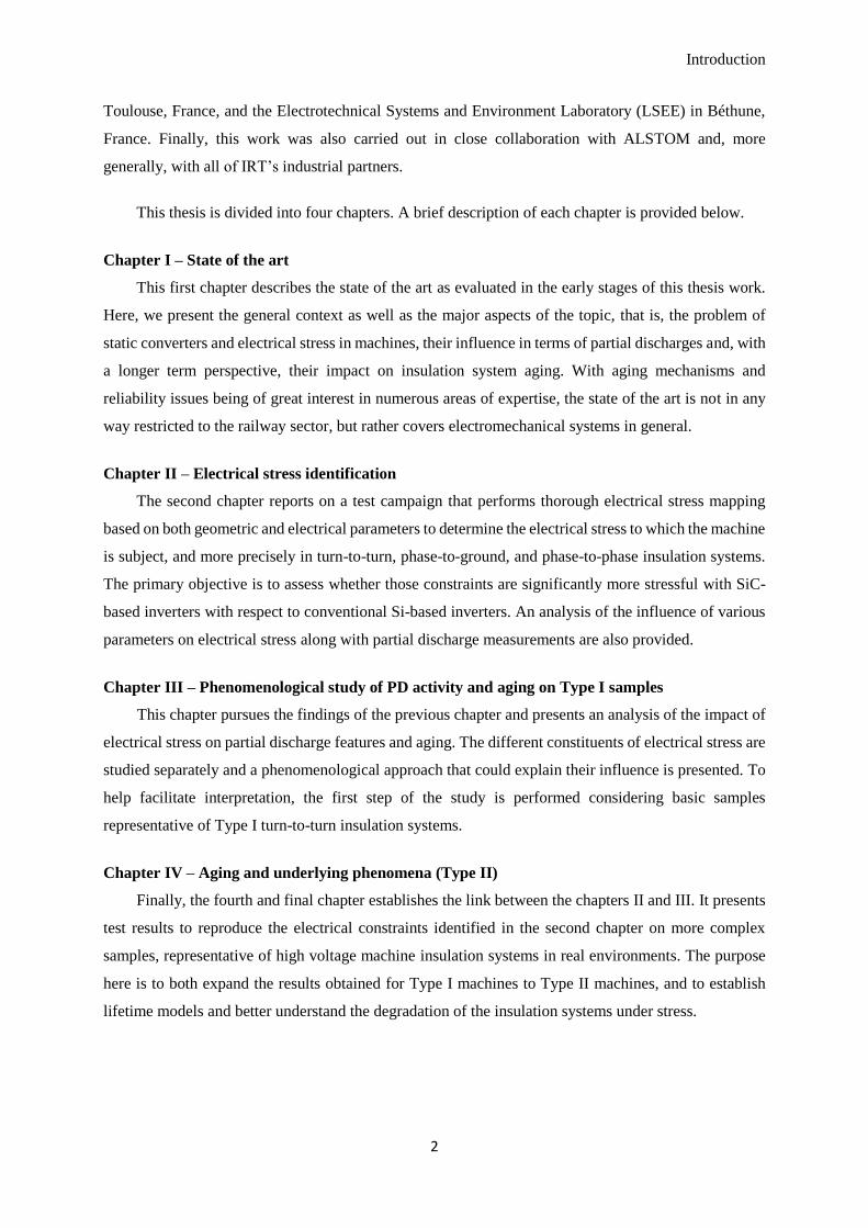
In the aeronautic industry, for example, the concept of “More Electrical Aircraft” was developed
with a view to increase efficiency, reliability, maintainability, cost-effectiveness, and finally to
rationalize the energy on board of aircraft by electrifying systems that today use hydraulic, pneumatic,
or mechanical energy [1]. The higher power density of electrical equipment is intended to drastically
reduce an aircraft’s weight, as well as its fuel consumption and environmental footprint.
The emergence of this phenomenon leads to increasing demands for energy and therefore to a
global increase of voltage levels, with the goal of generating and distributing more power without
increasing cable weight or their section. These new voltage levels bring unknown phenomena to this
industry that affect, among other things, electrical machines and, as a consequence, system reliability.
Figure I-1: Electrical power evolution in aeronautics [2]
State of the art
5
At the same time, ecological concerns also play a major role in thinking about the vehicles of
tomorrow. In recent years, the automotive industry has been pushed to find an alternative to replace
internal combustion vehicles, which are responsible for emitting a large volume of greenhouse gases
and fine particles. New solutions, such as hybrid and electrical vehicles, thus emerged to meet a growing
and never-ending string of recommendations. However, while that type of vehicle can be competitive
regarding urban traffic, their limited operating time and long battery recharging time, not to mention
financial considerations, are non-negligible obstacles to their development. One research track consists
of increasing the power density of motors while ensuring a lifetime long enough to enable the vehicle
to be cost-effective. With vehicle lifetime being linked mainly to the insulation system lifetime, the
automotive industry faces a problem similar to that of the aviation industry, despite different stakes and
challenges: combined with the use of power components, higher voltage levels compromise reliability,
and system aging must be studied and optimized in order to guarantee the required reliability.
The challenge of reliability, particularly through the aging and Partial Discharge (PD) phenomena,
is thus a central common point in various areas of expertise, including automotive and aeronautics fields,
as mentioned previously, but also railway. It turns out that rail transport, which is the primary context
of the work presented here, is somewhat different from the other cases. More details regarding its
specificities are presented below.
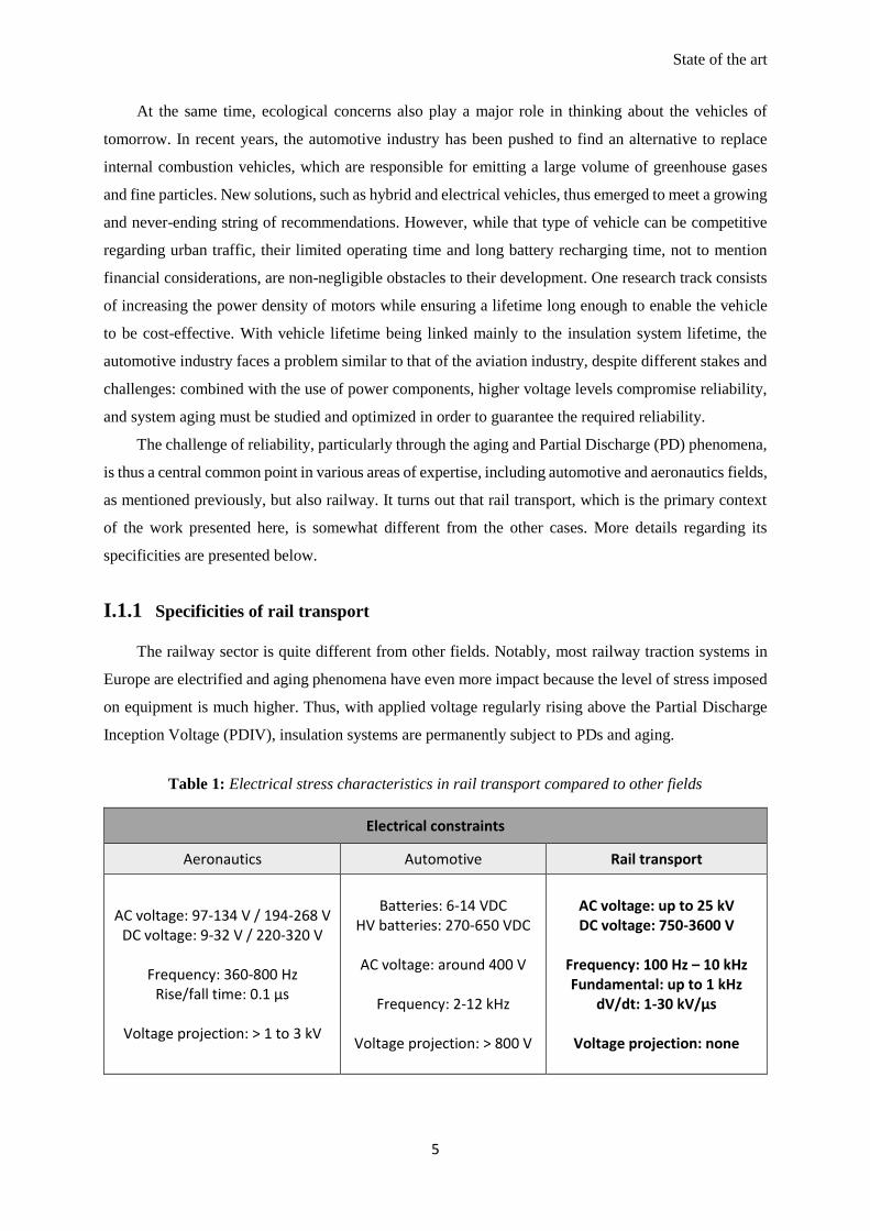
I.1.1 Specificities of rail transport
The railway sector is quite different from other fields. Notably, most railway traction systems in
Europe are electrified and aging phenomena have even more impact because the level of stress imposed
on equipment is much higher. Thus, with applied voltage regularly rising above the Partial Discharge
Inception Voltage (PDIV), insulation systems are permanently subject to PDs and aging.
Table 1: Electrical stress characteristics in rail transport compared to other fields
Electrical constraints
Aeronautics Automotive Rail transport
AC voltage: 97-134 V / 194-268 V DC voltage: 9-32 V / 220-320 V
Frequency: 360-800 Hz
Rise/fall time: 0.1 µs
Voltage projection: > 1 to 3 kV
Batteries: 6-14 VDC HV batteries: 270-650 VDC
AC voltage: around 400 V
Frequency: 2-12 kHz
Voltage projection: > 800 V
AC voltage: up to 25 kV DC voltage: 750-3600 V
Frequency: 100 Hz – 10 kHz Fundamental: up to 1 kHz
dV/dt: 1-30 kV/µs
Voltage projection: none
State of the art
6
Reliability is not a new area of focus. Numerous studies have already been performed on the topic.
However, the introduction of new fast-switching components in static converters brings a new
dimension to the problem of aging. Modern converters generate voltages with rise times between 50 ns
and 2 µs. Furthermore, the voltage at motor terminals depends on multiple characteristics specific to
inverter architecture, control, and interaction with other elements in the chain. All this makes the entire
issue of reliability equally crucial in rail transport as it is in for automotive and aviation sectors, for
example, but in separate context and for different reasons. In addition, in the today’s context of global
voltage increases mentioned previously, the specificities of rail transport can serve as a stepping stone
and strong incentive to study the mechanisms involved in the aging of high voltage machines that will
potentially be used to equip cars and airplanes of the future.
I.2 Partial discharge mechanisms
I.2.1 Partial discharge overview
A partial discharge (PD) is a fast and localized electrical discharge that only partially bridges the
insulation material between a conductor’s materials or electrodes. It does not lead to the immediate
breakdown of the insulation system, but it contributes to degradation via its mechanical, thermal, and
chemical effects when the electrical stress exceeds a critical value called partial discharge inception
voltage (PDIV). PDs occur in residual air gaps within insulation systems. These cavities may be open
or closed, but the physical phenomena are similar in both cases, as these cavities are often small in size
and contain a gas, generally air [3][4].
Electrostatic laws explain that electrical fields are higher in gaseous cavities than in polymer, as
polymer permittivity is greater than that of gas. The molecules inside a cavity are thus subject to a very
intense electric field, which sets an initial electron, originating from cosmic radiation or already present
for any other reason, into motion. This electron impacts the surrounding electrons belonging to
electrically neutral molecules. When the field is high enough, electrons can be snatched from the
molecules and, in turn, be set into motion by the electric field. Released electrons are likely to collide
with other molecules and, above a certain threshold, cause an electronic avalanche. When those
conditions are met, the gas inside the vacuole is ionized.
The Townsend mechanism bests represents the avalanche phenomenon, assuming a system with
two parallel plane metallic electrodes, and considering a uniform electric field. Two coefficients are
necessary to formalize the Townsend mechanism:
The first Townsend coefficient, α, depicts the avalanche effect.
The second Townsend coefficient, γ, depicts the secondary emission of electrons at the
cathode.
The ionization process is characterized by the first Townsend coefficient, which represents the ratio
of ionizing collisions per unit length. It is important to remember that only a fraction of the collisions
State of the art
7
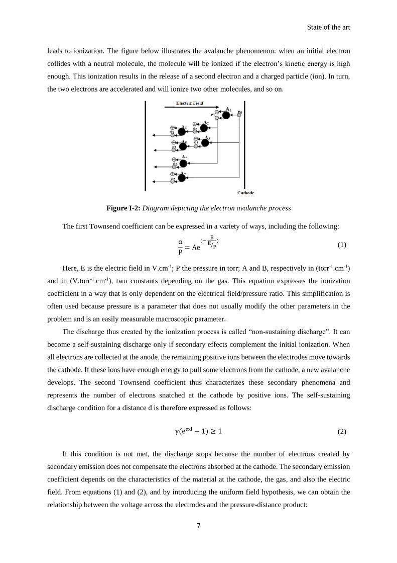
leads to ionization. The figure below illustrates the avalanche phenomenon: when an initial electron
collides with a neutral molecule, the molecule will be ionized if the electron’s kinetic energy is high
enough. This ionization results in the release of a second electron and a charged particle (ion). In turn,
the two electrons are accelerated and will ionize two other molecules, and so on.
Figure I-2: Diagram depicting the electron avalanche process
The first Townsend coefficient can be expressed in a variety of ways, including the following:
α
P= Ae
(− B
EP⁄
)
(1)
Here, E is the electric field in V.cm-1; P the pressure in torr; A and B, respectively in (torr-1.cm-1)
and in (V.torr-1.cm-1), two constants depending on the gas. This equation expresses the ionization
coefficient in a way that is only dependent on the electrical field/pressure ratio. This simplification is
often used because pressure is a parameter that does not usually modify the other parameters in the
problem and is an easily measurable macroscopic parameter.
The discharge thus created by the ionization process is called “non-sustaining discharge”. It can
become a self-sustaining discharge only if secondary effects complement the initial ionization. When
all electrons are collected at the anode, the remaining positive ions between the electrodes move towards
the cathode. If these ions have enough energy to pull some electrons from the cathode, a new avalanche
develops. The second Townsend coefficient thus characterizes these secondary phenomena and
represents the number of electrons snatched at the cathode by positive ions. The self-sustaining
discharge condition for a distance d is therefore expressed as follows:
γ(eαd − 1) ≥ 1 (2)
If this condition is not met, the discharge stops because the number of electrons created by
secondary emission does not compensate the electrons absorbed at the cathode. The secondary emission
coefficient depends on the characteristics of the material at the cathode, the gas, and also the electric
field. From equations (1) and (2), and by introducing the uniform field hypothesis, we can obtain the
relationship between the voltage across the electrodes and the pressure-distance product:
State of the art
8
V = BPd
ln (APd
ln (1 +1γ
))
(3)
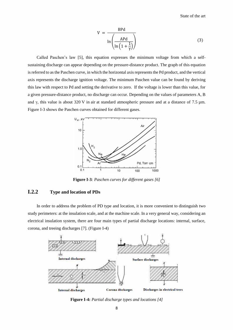
Called Paschen’s law [5], this equation expresses the minimum voltage from which a self-
sustaining discharge can appear depending on the pressure-distance product. The graph of this equation
is referred to as the Paschen curve, in which the horizontal axis represents the Pd product, and the vertical
axis represents the discharge ignition voltage. The minimum Paschen value can be found by deriving
this law with respect to Pd and setting the derivative to zero. If the voltage is lower than this value, for
a given pressure-distance product, no discharge can occur. Depending on the values of parameters A, B
and γ, this value is about 320 V in air at standard atmospheric pressure and at a distance of 7.5 µm.
Figure I-3 shows the Paschen curves obtained for different gases.
Figure I-3: Paschen curves for different gases [6]
I.2.2 Type and location of PDs
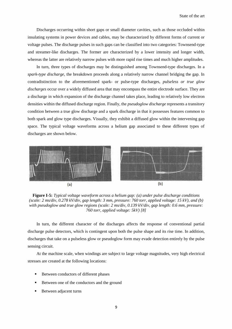
In order to address the problem of PD type and location, it is more convenient to distinguish two
study perimeters: at the insulation scale, and at the machine scale. In a very general way, considering an
electrical insulation system, there are four main types of partial discharge locations: internal, surface,
corona, and treeing discharges [7]. (Figure I-4)
Figure I-4: Partial discharge types and locations [4]
State of the art
9
Discharges occurring within short gaps or small diameter cavities, such as those occluded within
insulating systems in power devices and cables, may be characterized by different forms of current or
voltage pulses. The discharge pulses in such gaps can be classified into two categories: Townsend-type
and streamer-like discharges. The former are characterized by a lower intensity and longer width,
whereas the latter are relatively narrow pulses with more rapid rise times and much higher amplitudes.
In turn, three types of discharges may be distinguished among Townsend-type discharges. In a
spark-type discharge, the breakdown proceeds along a relatively narrow channel bridging the gap. In
contradistinction to the aforementioned spark- or pulse-type discharges, pulseless or true glow
discharges occur over a widely diffused area that may encompass the entire electrode surface. They are
a discharge in which expansion of the discharge channel takes place, leading to relatively low electron
densities within the diffused discharge region. Finally, the pseudoglow discharge represents a transitory
condition between a true glow discharge and a spark discharge in that it possesses features common to
both spark and glow type discharges. Visually, they exhibit a diffused glow within the intervening gap
space. The typical voltage waveforms across a helium gap associated to these different types of
discharges are shown below.
Figure I-5: Typical voltage waveform across a helium gap: (a) under pulse discharge conditions
(scale: 2 ms/div, 0.278 kV/div, gap length: 3 mm, pressure: 760 torr, applied voltage: 15 kV), and (b)
with pseudoglow and true glow regions (scale: 2 ms/div, 0.139 kV/div, gap length: 0.6 mm, pressure:
760 torr, applied voltage: 5kV) [8]
In turn, the different character of the discharges affects the response of conventional partial
discharge pulse detectors, which is contingent upon both the pulse shape and its rise time. In addition,
discharges that take on a pulseless glow or pseudoglow form may evade detection entirely by the pulse
sensing circuit.
At the machine scale, when windings are subject to large voltage magnitudes, very high electrical
stresses are created at the following locations:
Between conductors of different phases
Between one of the conductors and the ground
Between adjacent turns
State of the art
10
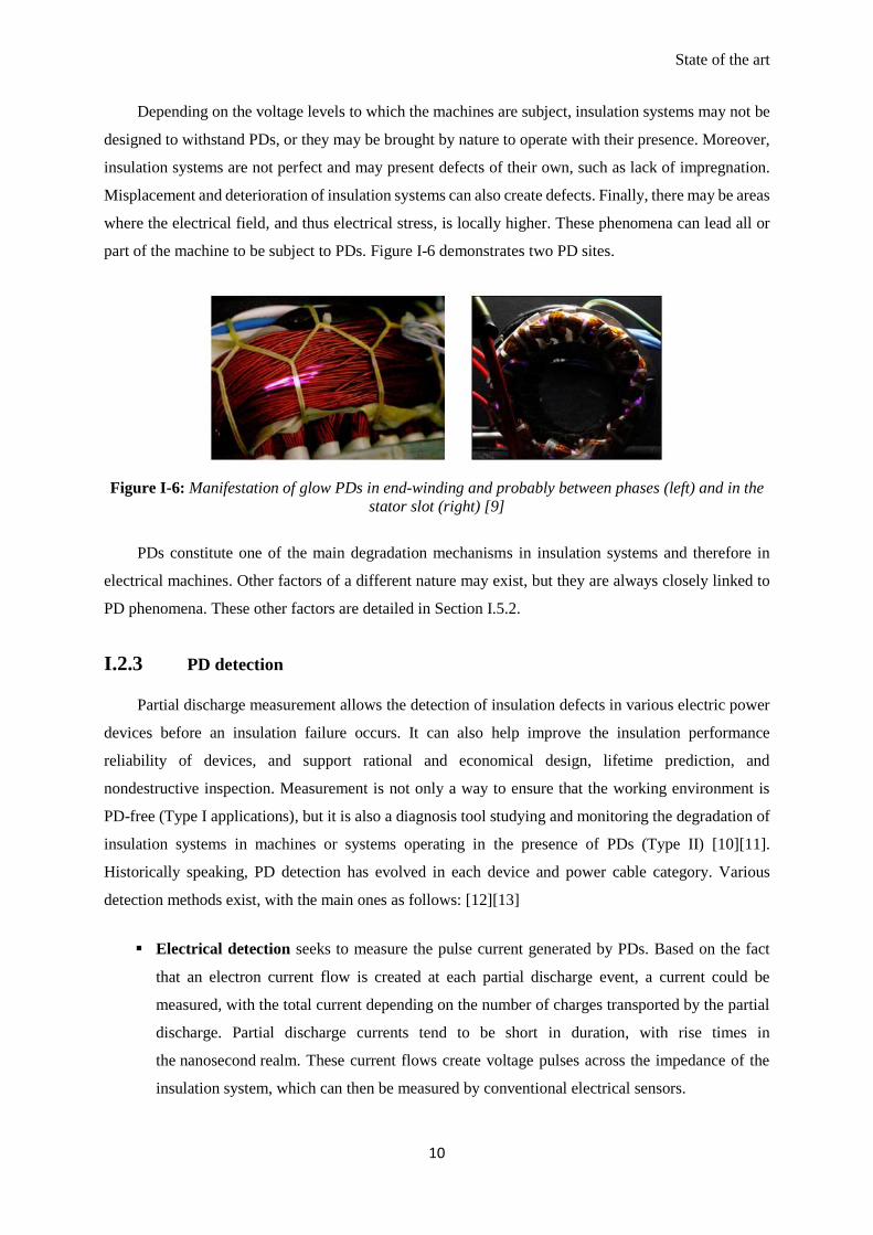
Depending on the voltage levels to which the machines are subject, insulation systems may not be
designed to withstand PDs, or they may be brought by nature to operate with their presence. Moreover,
insulation systems are not perfect and may present defects of their own, such as lack of impregnation.
Misplacement and deterioration of insulation systems can also create defects. Finally, there may be areas
where the electrical field, and thus electrical stress, is locally higher. These phenomena can lead all or
part of the machine to be subject to PDs. Figure I-6 demonstrates two PD sites.
Figure I-6: Manifestation of glow PDs in end-winding and probably between phases (left) and in the
stator slot (right) [9]
PDs constitute one of the main degradation mechanisms in insulation systems and therefore in
electrical machines. Other factors of a different nature may exist, but they are always closely linked to
PD phenomena. These other factors are detailed in Section I.5.2.
I.2.3 PD detection
Partial discharge measurement allows the detection of insulation defects in various electric power
devices before an insulation failure occurs. It can also help improve the insulation performance
reliability of devices, and support rational and economical design, lifetime prediction, and
nondestructive inspection. Measurement is not only a way to ensure that the working environment is
PD-free (Type I applications), but it is also a diagnosis tool studying and monitoring the degradation of
insulation systems in machines or systems operating in the presence of PDs (Type II) [10][11].
Historically speaking, PD detection has evolved in each device and power cable category. Various
detection methods exist, with the main ones as follows: [12][13]
Electrical detection seeks to measure the pulse current generated by PDs. Based on the fact
that an electron current flow is created at each partial discharge event, a current could be
measured, with the total current depending on the number of charges transported by the partial
discharge. Partial discharge currents tend to be short in duration, with rise times in
the nanosecond realm. These current flows create voltage pulses across the impedance of the
insulation system, which can then be measured by conventional electrical sensors.
State of the art
11
Electromagnetic measurement consists of measuring the high frequency electromagnetic
waves generated by PDs and propagating away from the discharge location site in the gaseous
medium. The discharge spectrum ranges from a few hundred kHz to several hundred MHz. With
a suitable antenna, it is thus possible to detect PDs and obtain information regarding the
magnitude of the discharge and its generation point.
Optical detection is based on the fact that partial discharges also dissipate energy in the form
of light. Measuring the light generated from the discharge with an adequate device, such as a
photomultiplier, thus makes it possible to evaluate the discharge characteristics and provides
another way of detecting and locating PDs.
Finally, the mechanical vibration and sound generated by partial discharges can be converted
and detected by means of acoustic measurement methods.
There is no universality in PD detection technology that is available to all kinds of power
equipment. The choice of a detection method must take into account the nature of the detection (on-
line/off-line), equipment structure, surrounding noise, similarities and differences among PD detection
technologies and signal processing, as well as the desired criteria for equipment analysis. Furthermore,
discharges that exhibit a glow or pseudo-glow character could fail to excite the response of conventional
pulse-type discharge. In practical terms, this means that the detection device choice also depends on the
discharge type. In that respect, electrical and electromagnetic devices are more suited for detecting
spark-type discharges, whereas optical or acoustic detection methods are preferred in the case of glow
or pseudoglow discharges.
PDs and their features are heavily influenced by voltage signal characteristics, which can cause
modifications in terms of the electrical field and also affect detection. It is thus necessary to take those
characteristics into account and define the extent to which the voltage shape used to supply the machine
could be an aggravating factor. Investigations on voltage shapes induced by static converters will be
covered in the following sections.
I.3 Electromechanical chain
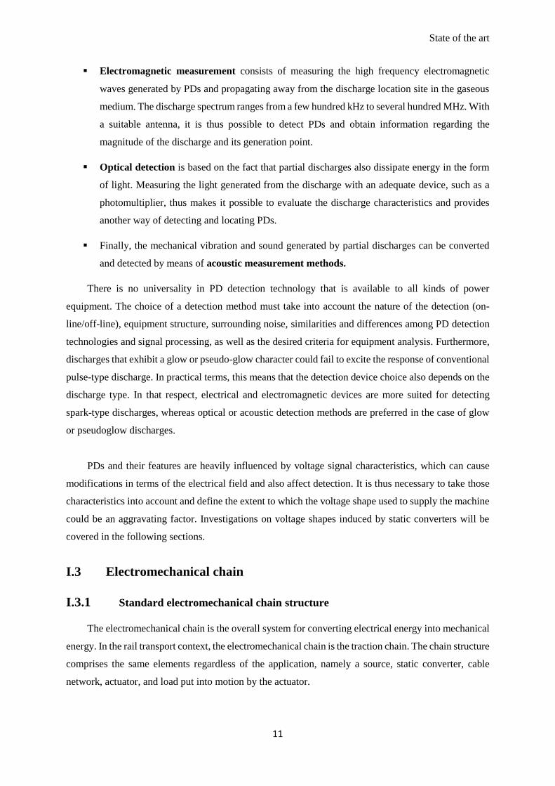
I.3.1 Standard electromechanical chain structure
The electromechanical chain is the overall system for converting electrical energy into mechanical
energy. In the rail transport context, the electromechanical chain is the traction chain. The chain structure
comprises the same elements regardless of the application, namely a source, static converter, cable
network, actuator, and load put into motion by the actuator.
State of the art
12
The electromechanical chain aims to receive, convert, and distribute the electrical energy. The input
voltage type and level vary depending on the grid. It is thus necessary to adapt voltage in order to supply
the equipment.
Figure I-7: Schematic drawing of a railway traction system (load not represented)
A converter (generally an inverter) converts the DC bus voltage from the grid into a voltage that
can be used by the actuator. Converters use power electronic components such as Silicon-based IGBTs
(Insulated Gate Bipolar Transistors), which have been the benchmark in terms of controlled switches
for several decades. However, wide bandgap components such as SiC (Silicon Carbide) and GaN
(Gallium Nitride)-based components are gradually replacing those technologies, mainly thanks to their
fast rise and fall times which considerably reduce switching losses. Inverters are usually controlled using
the Pulse Width Modulation (PWM) technique. The PWM operating principle will be reviewed in the
next section.
Cables make the connection between the inverter output and the machine input in order to transport
the electrical energy. Adverse effects related to cable length, nature, and disposition can occur and must
be taken into account or suppressed to ensure proper machine operation.
The motor is the energy conversion element. There are several types of actuators depending on
the application. In aeronautics or automotive applications, for example, permanent magnet synchronous
machines, which ensure high power density, are preferred; whereas asynchronous motors might often
be used in rail transport.
Finally, filters can be placed at the inverter input or output. Filters can be convenient for various
functional reasons or to meet specific standards.
I.3.2 Type I/Type II machines: what is the difference?
Rather than differentiate machines by sector and by application, it is far more convenient to
distinguish them according to their operating voltage. The IEC 60034-18-41 [14] and 60034-18-42 [15]
standards address this problem by proposing classification into two categories: Type I and Type II
machines, depending on whether they are intended to operate with (Type II) or without (Type I) PDs at
State of the art
13
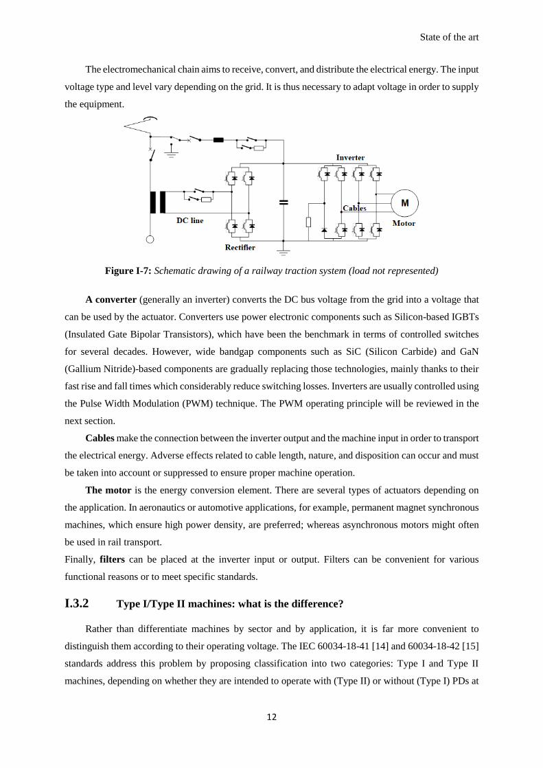
any point in the insulation system. Type I insulation systems are commonly used in low voltage rotating
machines (< 700V) and are composed of random-wound coils. If any part of the insulation system is
likely to undergo PDs during its life cycle, the system is defined as a Type II insulation system, and
subsequently it must be comprised of PD-resistant materials. Machines with a nominal voltage higher
than 700V generally use Type II insulation systems [16].
This classification thus enables us to treat low voltage and high voltage machines differently. Even
if aging mechanisms are the same or very similar (which is not fully guaranteed), insulation systems are
not supposed to present the same behavior in the presence of PDs. Furthermore, low voltage machines
generally use random-wound coils, whereas high voltage machines use formed-wound coils. In random-
wound coils, the conductor insulation is quite thin and often surrounded by air. It may also happen that
the first and last turn of a coil are adjacent to each other, leading to an increased probability of PD
inception, particularly between turns, if the voltage is high enough. The erosion caused by PDs may
cause unnecessary damage to the insulation system; it is therefore crucial to ensure that no PDs can
occur.
Figure I-8: Illustration of partial discharge in air between several conductors under high stress [16]
In the case of Type II machines, insulation systems are reinforced with materials that are highly
resistant to erosion caused by PDs. They can therefore operate in the presence of PDs; aging is not
eliminated, but it is slowed considerably.
The choice of insulating materials is an important issue when designing and constructing a
machine. It is thus particularly important to characterize the mechanisms associated with PDs in order
to select the most appropriate insulation system. Because of the wide variety of available insulating
materials, it is appropriate to review the main types of insulation typically used in machines.
I.3.3 Insulation system state of the art
In the previous section, we presented the distinction between Type I and Type II insulation systems.
It is important to point out that when the operating voltage of a machine is below 700V, it may include
both Type I and Type II insulation systems. However, Type II insulation systems are required for
machines with an RMS voltage value beyond 700V.
Electrical insulation systems are divided into several temperature classes which specify the
insulation withstand, and which are defined according to tests described in the IEC 60085 standard. It
State of the art
14
should be noted that other organizations such as NEMA define the same type of standards. These thermal
indexes correspond to the maximal temperature for which a material can be used for at least 20,000
hours without reaching a pre-established end of life criteria. Table 2 presents the existing classes and
the associated temperature ranges according to IEC 60085 and NEMA standards.
Table 2: Definition of thermal classes according to IEC 60085 (1) and NEMA (2)
Relative thermal endurance index (°C)
Thermal class (°C) Designation
90 ≤ to < 105 90 Y (1)
105 ≤ to < 120 105 A (1)
120 ≤ to < 130 120 E (1)
130 ≤ to < 155 130 B (1)
155 ≤ to < 180 155 F (1)
180 ≤ to < 200 180 H (1)
200 ≤ to < 220 200 N (2)
220 ≤ to < 250 220 R (2)
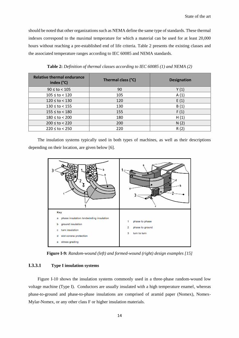
The insulation systems typically used in both types of machines, as well as their descriptions
depending on their location, are given below [6].
Figure I-9: Random-wound (left) and formed-wound (right) design examples [15]
I.3.3.1 Type I insulation systems
Figure I-10 shows the insulation systems commonly used in a three-phase random-wound low
voltage machine (Type I). Conductors are usually insulated with a high temperature enamel, whereas
phase-to-ground and phase-to-phase insulations are comprised of aramid paper (Nomex), Nomex-
Mylar-Nomex, or any other class F or higher insulation materials.
State of the art
15
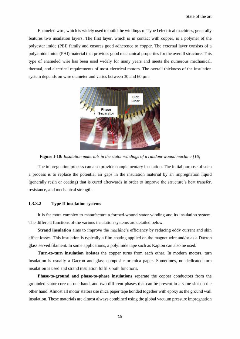
Enameled wire, which is widely used to build the windings of Type I electrical machines, generally
features two insulation layers. The first layer, which is in contact with copper, is a polymer of the
polyester imide (PEI) family and ensures good adherence to copper. The external layer consists of a
polyamide imide (PAI) material that provides good mechanical properties for the overall structure. This
type of enameled wire has been used widely for many years and meets the numerous mechanical,
thermal, and electrical requirements of most electrical motors. The overall thickness of the insulation
system depends on wire diameter and varies between 30 and 60 µm.
Figure I-10: Insulation materials in the stator windings of a random-wound machine [16]
The impregnation process can also provide complementary insulation. The initial purpose of such
a process is to replace the potential air gaps in the insulation material by an impregnation liquid
(generally resin or coating) that is cured afterwards in order to improve the structure’s heat transfer,
resistance, and mechanical strength.
I.3.3.2 Type II insulation systems
It is far more complex to manufacture a formed-wound stator winding and its insulation system.
The different functions of the various insulation systems are detailed below.
Strand insulation aims to improve the machine’s efficiency by reducing eddy current and skin
effect losses. This insulation is typically a film coating applied on the magnet wire and/or as a Dacron
glass served filament. In some applications, a polyimide tape such as Kapton can also be used.
Turn-to-turn insulation isolates the copper turns from each other. In modern motors, turn
insulation is usually a Dacron and glass composite or mica paper. Sometimes, no dedicated turn
insulation is used and strand insulation fulfills both functions.
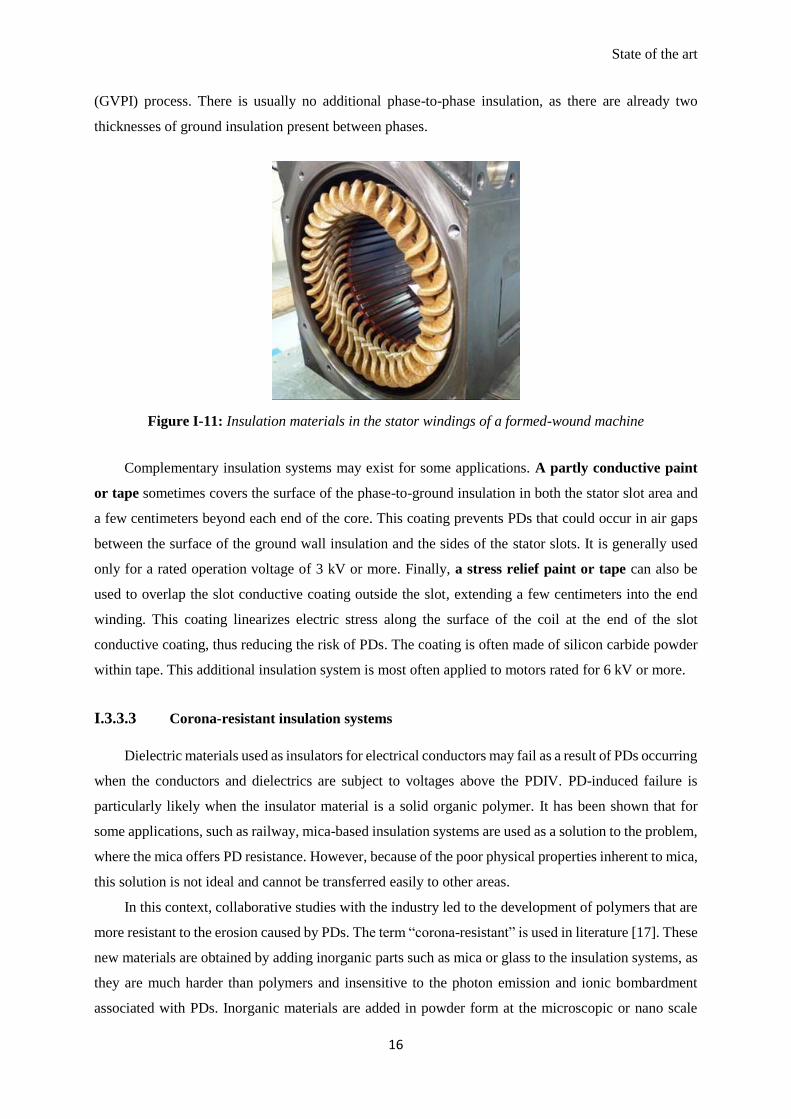
Phase-to-ground and phase-to-phase insulations separate the copper conductors from the
grounded stator core on one hand, and two different phases that can be present in a same slot on the
other hand. Almost all motor stators use mica paper tape bonded together with epoxy as the ground wall
insulation. These materials are almost always combined using the global vacuum pressure impregnation
State of the art
16
(GVPI) process. There is usually no additional phase-to-phase insulation, as there are already two
thicknesses of ground insulation present between phases.
Figure I-11: Insulation materials in the stator windings of a formed-wound machine
Complementary insulation systems may exist for some applications. A partly conductive paint
or tape sometimes covers the surface of the phase-to-ground insulation in both the stator slot area and
a few centimeters beyond each end of the core. This coating prevents PDs that could occur in air gaps
between the surface of the ground wall insulation and the sides of the stator slots. It is generally used
only for a rated operation voltage of 3 kV or more. Finally, a stress relief paint or tape can also be
used to overlap the slot conductive coating outside the slot, extending a few centimeters into the end
winding. This coating linearizes electric stress along the surface of the coil at the end of the slot
conductive coating, thus reducing the risk of PDs. The coating is often made of silicon carbide powder
within tape. This additional insulation system is most often applied to motors rated for 6 kV or more.
I.3.3.3 Corona-resistant insulation systems
Dielectric materials used as insulators for electrical conductors may fail as a result of PDs occurring
when the conductors and dielectrics are subject to voltages above the PDIV. PD-induced failure is
particularly likely when the insulator material is a solid organic polymer. It has been shown that for
some applications, such as railway, mica-based insulation systems are used as a solution to the problem,
where the mica offers PD resistance. However, because of the poor physical properties inherent to mica,
this solution is not ideal and cannot be transferred easily to other areas.
In this context, collaborative studies with the industry led to the development of polymers that are
more resistant to the erosion caused by PDs. The term “corona-resistant” is used in literature [17]. These
new materials are obtained by adding inorganic parts such as mica or glass to the insulation systems, as
they are much harder than polymers and insensitive to the photon emission and ionic bombardment
associated with PDs. Inorganic materials are added in powder form at the microscopic or nano scale
State of the art
17
[18][19]. The quality of the insulation layers depends on the distribution of these micro or nanoparticles
in the polymers. It is particularly challenging to obtain a uniform mixture before polymerization,
especially when the inorganic powders are at the nano scale, notably because nanoparticles have high
surface energy and naturally tend to form agglomerates or aggregates.
The resulting corona-resistant materials effectively prevent PD degradation of insulation leading to
motor failure in normal use. Besides, the glass or mica composite occupies space in the core which
otherwise could accommodate additional copper and thereby reduce the size of the motor.
I.4 About electrical stress in machines
I.4.1 Static converters and PWM-like signals
For several reasons, notably to minimize losses, it is necessary for the current flowing through the
windings of an electrical machine to have a sinusoidal shape. Generally, this is possible only if the
voltage signal also is sinusoidal. In the past, it was standard practice to use direct current machines for
applications requiring variable speed control. Indeed, by varying voltage, it is possible to modify rotation
speed accordingly. AC motors were only used for applications requiring fixed speed.
Today, generating sinusoidal signals for powering machines has become widespread and is now a
reference for many reasons, including improved cost-efficiency and greater efficiency. Moreover, the
harmonic content of such machines must be controlled in order to meet specified standards. Furthermore,
a sinusoidal current shape makes it possible to rephase the voltage and current signals to reach a unity
power factor if necessary.
In order to generate such sinusoidal signals, semiconductor components are used in association
with the Pulse Width Modulation (PWM) strategy at very high switching frequencies. Speed variation
is thus achieved via an inverter that generates high frequency voltage impulses with variable width at
each phase in order to reconstruct a signal with varying fundamental frequency at the motor terminals,
while rejecting harmonic content. The rise times associated with semiconductor components as they
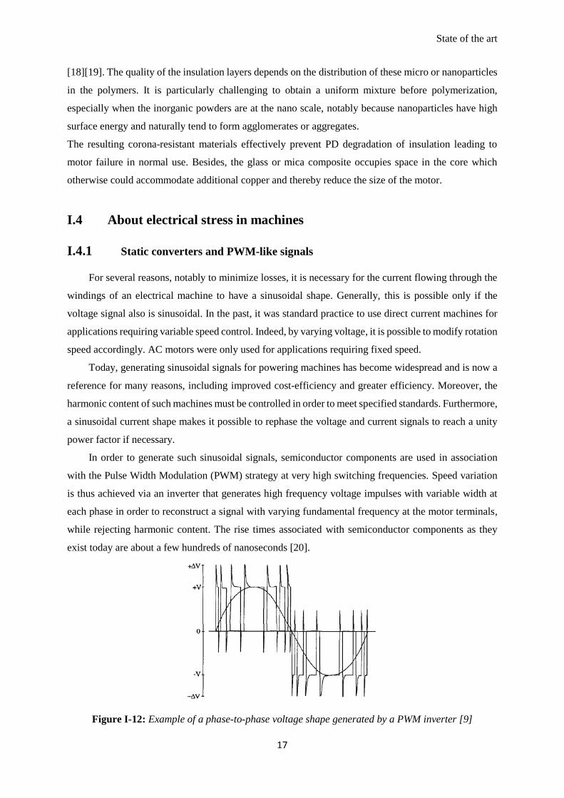
exist today are about a few hundreds of nanoseconds [20].
Figure I-12: Example of a phase-to-phase voltage shape generated by a PWM inverter [9]
State of the art
18
Therefore, static converters controlled by PWM generate steep voltage slopes that create high
frequency oscillatory behaviors in machine windings. It is thus necessary to characterize those
undesirable phenomena, which result in previously nonexistent dysfunctions that may affect system
reliability.
Pulse width modulation is a method for controlling the average power delivered by an electrical
signal by effectively slicing it up into discrete parts. Consequently, an inverter using this control method
is a voltage source whose magnitude, frequency, and “shape” are controllable. Due to its structure
composed of two bidirectional switching cells, the voltage inverter is reversible on the condition that
this is also the case for the DC source. For most applications, the idea is to generate a sinusoidal current
waveform. The rate (or frequency) at which the power supply must switch, as well as the necessity to
add or not add a filtering device, can vary greatly depending on the load and application. Several types
of PWM control strategies exist [21]; the choice of a strategy is mainly dependent on the supply voltage,
frequency, rotation speed of the motor, and above all, the user requirements regarding harmonic content
suppression, torque ripple, loss management and, more broadly, desired performance.
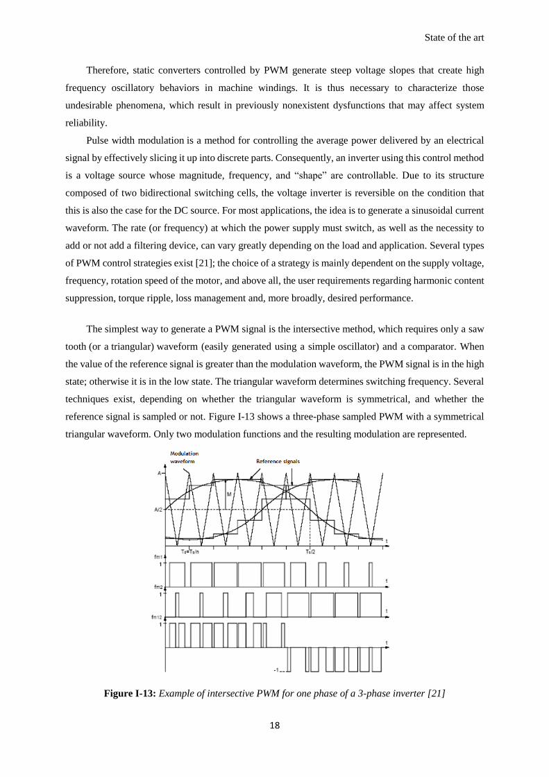
The simplest way to generate a PWM signal is the intersective method, which requires only a saw
tooth (or a triangular) waveform (easily generated using a simple oscillator) and a comparator. When
the value of the reference signal is greater than the modulation waveform, the PWM signal is in the high
state; otherwise it is in the low state. The triangular waveform determines switching frequency. Several
techniques exist, depending on whether the triangular waveform is symmetrical, and whether the
reference signal is sampled or not. Figure I-13 shows a three-phase sampled PWM with a symmetrical
triangular waveform. Only two modulation functions and the resulting modulation are represented.
Figure I-13: Example of intersective PWM for one phase of a 3-phase inverter [21]
State of the art
19
There are several subtypes of intersective PWMs, depending on whether they are synchronous or
asynchronous, analog or digital or even depending on the symmetry of the triangular waveform; for the
sake of brevity, those subcategories will not be detailed here [22] [23].
Along with these two main types of PWM control, several other types of methods exist and are
used for controlling electrical machines. SVM (Space Vector Modulation) is one of the most efficient
advanced methods of modulation, in particular for applications with variable frequency. Its use has
gradually increased in recent years due to its robust performance. Numerous types of SVM exist, and
the differences between them mainly lie in their quality and implementation requirements. The main
interest of this kind of strategy is the reduction of total harmonic distortion (THD) associated with fast
switching of the PWM. In delta modulation, the output signal is integrated and the result is compared
to limits, which correspond to a reference signal offset by a constant. Every time the integral of the
output signal reaches one of the limits, the PWM signal changes state. In delta-sigma modulation, the
output signal is subtracted from a reference signal to form an error signal and the output changes state
when the integral of the error exceeds the limits. Direct torque control is a method used to control AC
motors. It is closely related with delta modulation. Motor torque and magnetic flux are estimated and
then controlled to stay within their hysteresis bands by turning on a new combination of the device's
semiconductor switches each time either of the signals tries to deviate outside the band. The pre-
calculated PWM method consists of pre-calculating switching moments of power semiconductor
modules to suppress specified harmonics in the inverter output voltage. Finally, a direct full-wave
command can be used in some applications and under specific conditions, generally to take full
advantage of available voltage while avoiding or minimizing inverter losses.
I.4.2 Impact of using PWM control
Numerous studies have been performed on electrical machines supplied by static converters [24]
[25] [10]. In most cases, the studies tend to show a drastic rise of the failure rate coinciding with the
presence of pulse signals with increasingly fast rise times and switching frequencies. The accelerated
degradation of insulation systems, and as a result that of machines, is thus a direct consequence of the
use of such signals generated by PWM commands. This section presents the main impact of PWM
control on voltage stress and, in turn, on a machine’s insulation systems.
I.4.2.1 Rising edges and non-linear voltage distribution
Low voltage electrical machines, as highlighted above, often consist of random-wound coils whose
turns can be raised to vastly different potentials during the transitional regime following the voltage
rising edge. Given that the exact position of these turns in the slots is relatively random, there is a chance
State of the art
20
for the first and last turn to be adjacent to each other. The probability to be in such an extremely
unfavorable situation, with high potential differences between turns, is non-negligible.
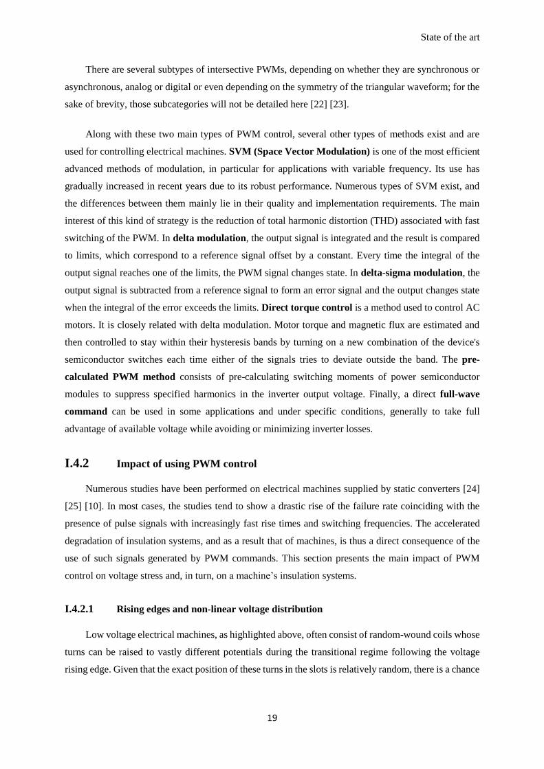
Figure I-14 is the result of a statistical study [26] carried out on a slot containing 41 wires ordered
in successive layers from the end of the slot. This extremely favorable case is very unlikely to occur. In
order to calculate the probability of adjacency, a very large number of equiprobable selections of wire
distribution in the slot are realized according to the Monte-Carlo method. The right-hand side of the
figure shows the geometrical analysis of all the adjacencies for the purpose of determining the maximum
turn number difference between two conductors at any point of the slot.
Figure I-14: Cross-sectional view of the slot and adjacency likelihood vs turn number difference [27]
The above graph shows that the probability of having the input conductor next to the output
conductor is about 12%. It is thus necessary to ensure that the turn-to-turn insulation is able to bear the
total voltage at the coil terminals.
In addition, when the machine undergoes very steep voltage slopes, the voltage distribution in the
coils can no longer be considered as linear. Characterizing these high frequency effects is complex and
must take into account all the parasitic effects related to these switching edges. A number of approaches
can be adopted, such as the equivalent circuit method or the Multiconductor Transmission Line (MTL)
theory; all these methods are based on rewriting Maxwell’s equations to take parasitic elements into
account [28]. The latter (capacitance, inductance, resistance, and conductance) are most often calculated
using finite element computation and integrated into numerical models of the machine. In substance, it
is shown that the rising edges are less steep as the voltage propagates in the coil. The slope is thus slowed
and the oscillations following the maximum voltage tend to mitigate. Hence, the voltages in the windings
are distributed and handled by complex transitory regimes, especially when the relative position of each
turn is unknown.
State of the art
21
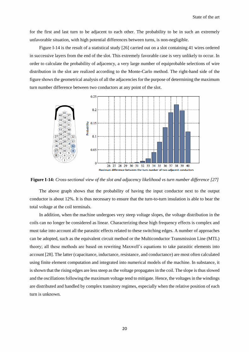
Figure I-15: Voltage distribution in the 41 turns of a coil [26]
I.4.2.2 Overvoltages
The fast voltage slopes transiting through the inverter, cables, and machine can also cause
overvoltage phenomena. These overvoltages should not exist in the first place, and the insulation
systems are not always designed to cope with those types of stress. The wave reflection phenomenon is
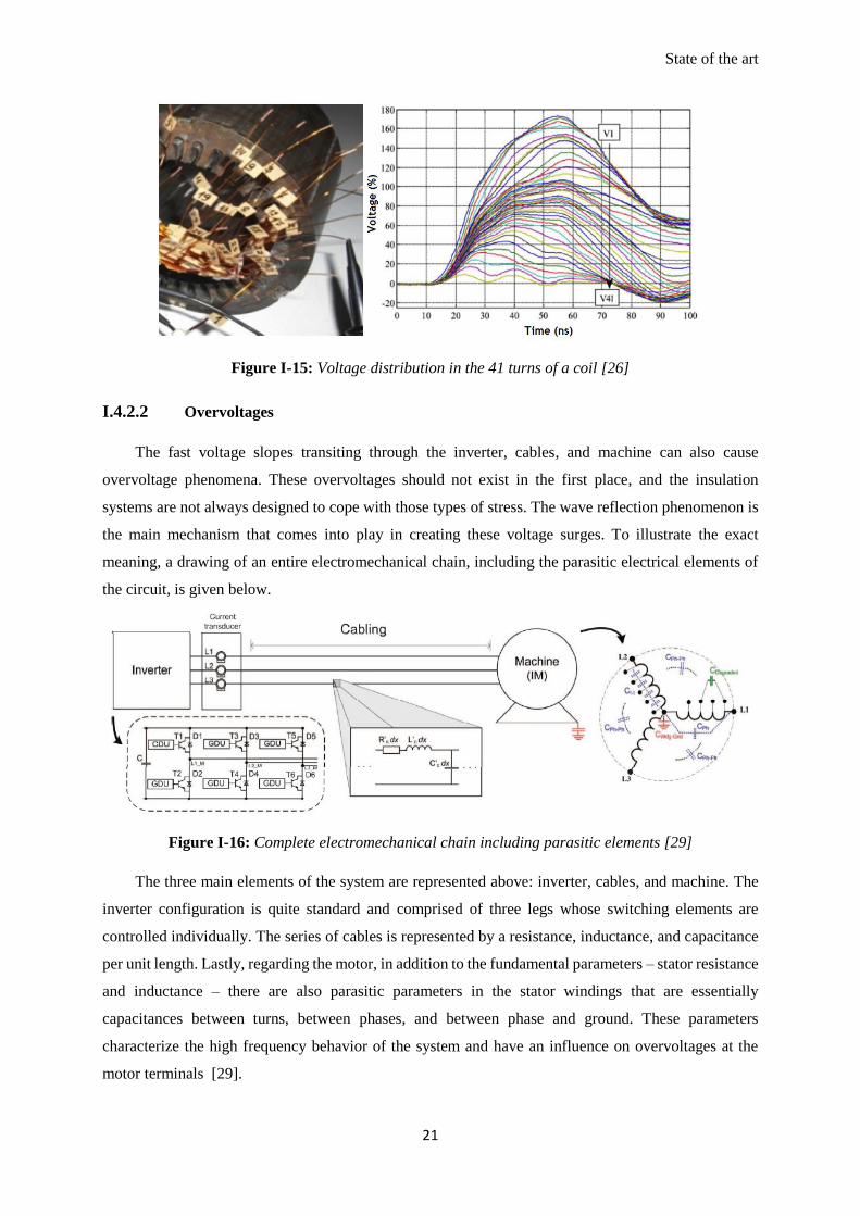
the main mechanism that comes into play in creating these voltage surges. To illustrate the exact
meaning, a drawing of an entire electromechanical chain, including the parasitic electrical elements of
the circuit, is given below.
Figure I-16: Complete electromechanical chain including parasitic elements [29]
The three main elements of the system are represented above: inverter, cables, and machine. The
inverter configuration is quite standard and comprised of three legs whose switching elements are
controlled individually. The series of cables is represented by a resistance, inductance, and capacitance
per unit length. Lastly, regarding the motor, in addition to the fundamental parameters – stator resistance
and inductance – there are also parasitic parameters in the stator windings that are essentially
capacitances between turns, between phases, and between phase and ground. These parameters
characterize the high frequency behavior of the system and have an influence on overvoltages at the
motor terminals [29].
State of the art
22
While the phenomena are considered to be very fast, the equivalent impedance of the converter is
very low compared to that of the cable, the latter itself being very low compared to that of the motor for
high frequencies that are likely to cause resonance. This impedance mismatch between the three
elements leads to reflection phenomena at both ends of the cable whose consequences depend mainly
on cable geometry and length.
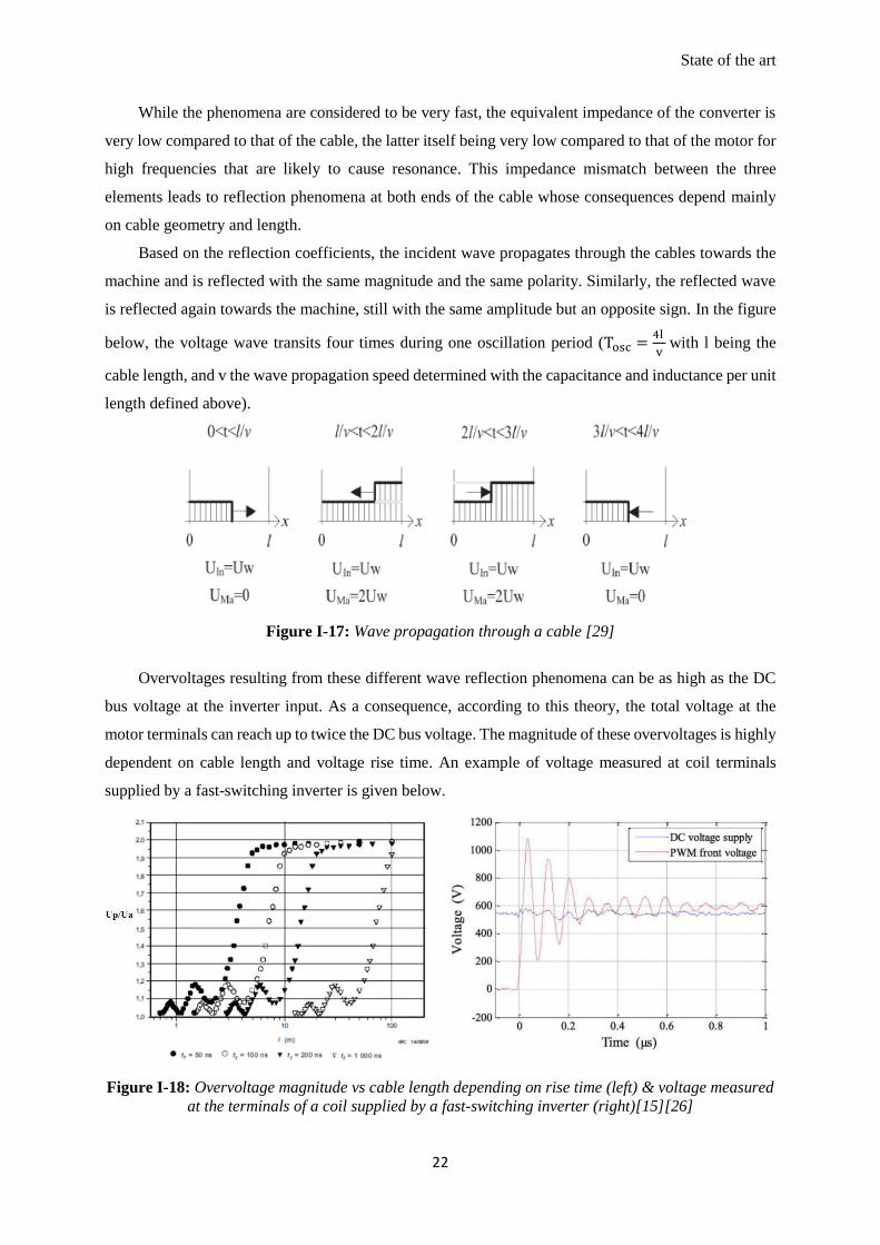
Based on the reflection coefficients, the incident wave propagates through the cables towards the
machine and is reflected with the same magnitude and the same polarity. Similarly, the reflected wave
is reflected again towards the machine, still with the same amplitude but an opposite sign. In the figure
below, the voltage wave transits four times during one oscillation period (Tosc =4l
v with l being the
cable length, and v the wave propagation speed determined with the capacitance and inductance per unit
length defined above).
Figure I-17: Wave propagation through a cable [29]
Overvoltages resulting from these different wave reflection phenomena can be as high as the DC
bus voltage at the inverter input. As a consequence, according to this theory, the total voltage at the
motor terminals can reach up to twice the DC bus voltage. The magnitude of these overvoltages is highly
dependent on cable length and voltage rise time. An example of voltage measured at coil terminals
supplied by a fast-switching inverter is given below.
Figure I-18: Overvoltage magnitude vs cable length depending on rise time (left) & voltage measured
at the terminals of a coil supplied by a fast-switching inverter (right)[15][26]
State of the art
23
The main impact of this overvoltage increase in terms of amplitude, frequency, non-linearity, and
rising edge, is an increase of PD activity [30][31]. A general review of the harmful effects linked to such
phenomena and depending on voltage shape, among other things, is detailed in Paragraph I.5, which is
exclusively dedicated to the aging of insulation systems.
I.4.2.3 PD measurement under PWM signals
PD detection is a particularly tricky problem when it must be performed in presence of very fast
rise and fall times, such as those imposed by Si IGBT (Insulated Gate Bipolar Transistor) or SiC
MOSFET (Metal Oxide Semiconductor Field Effect Transistor) switches. Under such operational
conditions, it is crucial to select the most adequate detection tool to be able to detect PDs as effectively
as possible.
The efficiency of most PD detection methods has been proven for DC or sinusoidal input voltages
[32][33]. Concerning impulse voltage, however, the detection – particularly electrical detection –
becomes far more complex due to switching noise. Indeed, the noise generated by power component
switching tends to overlap with PD signals, which mainly occur at maximum voltage, i.e. during the
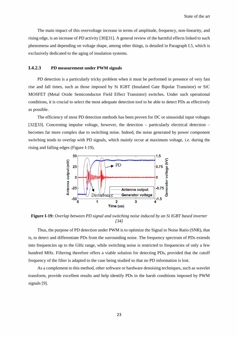
rising and falling edges (Figure I-19).
Figure I-19: Overlap between PD signal and switching noise induced by an Si IGBT based inverter
[34]
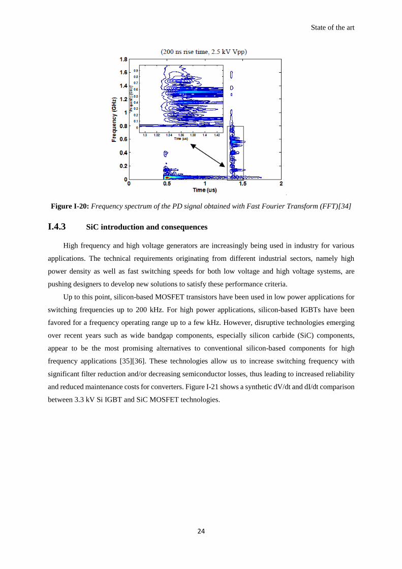
Thus, the purpose of PD detection under PWM is to optimize the Signal to Noise Ratio (SNR), that
is, to detect and differentiate PDs from the surrounding noise. The frequency spectrum of PDs extends
into frequencies up to the GHz range, while switching noise is restricted to frequencies of only a few
hundred MHz. Filtering therefore offers a viable solution for detecting PDs, provided that the cutoff
frequency of the filter is adapted to the case being studied so that no PD information is lost.
As a complement to this method, other software or hardware denoising techniques, such as wavelet
transform, provide excellent results and help identify PDs in the harsh conditions imposed by PWM
signals [9].
State of the art
24
Figure I-20: Frequency spectrum of the PD signal obtained with Fast Fourier Transform (FFT)[34]
I.4.3 SiC introduction and consequences
High frequency and high voltage generators are increasingly being used in industry for various
applications. The technical requirements originating from different industrial sectors, namely high
power density as well as fast switching speeds for both low voltage and high voltage systems, are
pushing designers to develop new solutions to satisfy these performance criteria.
Up to this point, silicon-based MOSFET transistors have been used in low power applications for
switching frequencies up to 200 kHz. For high power applications, silicon-based IGBTs have been
favored for a frequency operating range up to a few kHz. However, disruptive technologies emerging
over recent years such as wide bandgap components, especially silicon carbide (SiC) components,
appear to be the most promising alternatives to conventional silicon-based components for high
frequency applications [35][36]. These technologies allow us to increase switching frequency with
significant filter reduction and/or decreasing semiconductor losses, thus leading to increased reliability
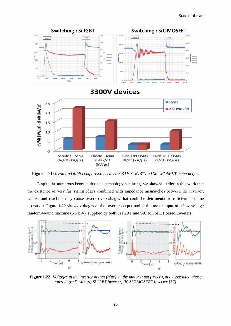
and reduced maintenance costs for converters. Figure I-21 shows a synthetic dV/dt and dI/dt comparison
between 3.3 kV Si IGBT and SiC MOSFET technologies.
State of the art
25
Figure I-21: dV/dt and dI/dt comparison between 3.3 kV Si IGBT and SiC MOSFET technologies
Despite the numerous benefits that this technology can bring, we showed earlier in this work that
the existence of very fast rising edges combined with impedance mismatches between the inverter,
cables, and machine may cause severe overvoltages that could be detrimental to efficient machine
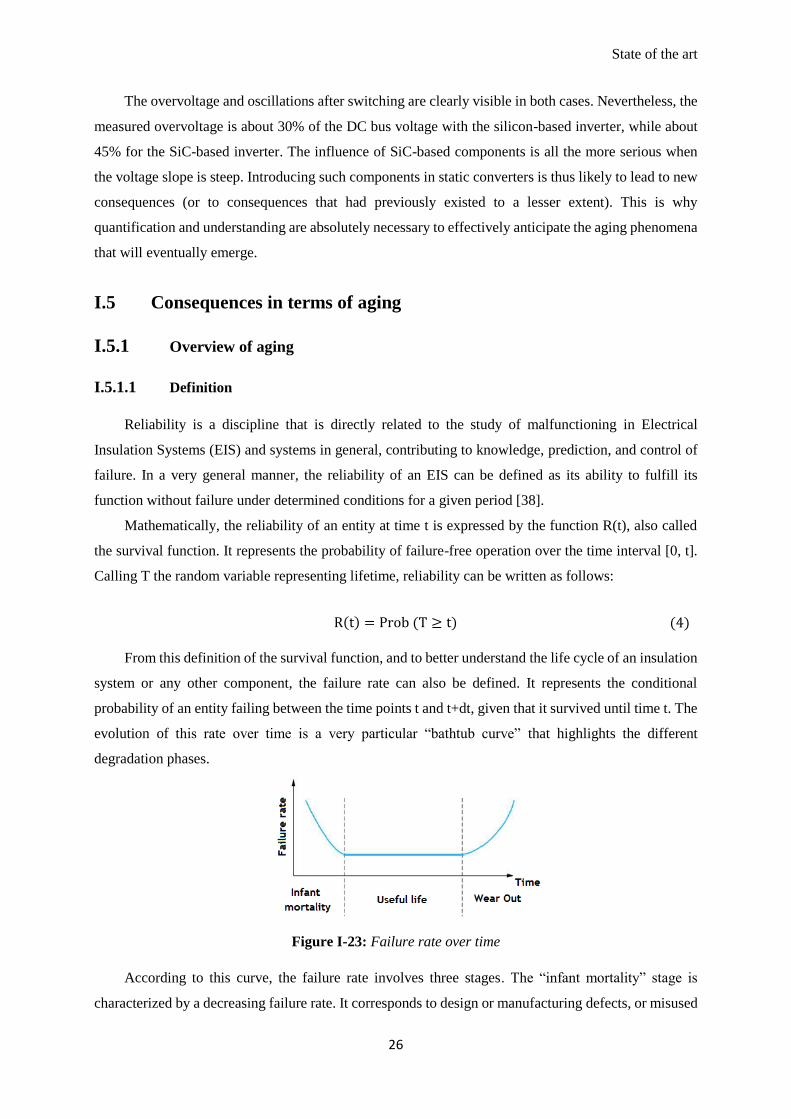
operation. Figure I-22 shows voltages at the inverter output and at the motor input of a low voltage
random-wound machine (5.5 kW), supplied by both Si IGBT and SiC MOSFET based inverters.
Figure I-22: Voltages at the inverter output (blue), at the motor input (green), and associated phase
current (red) with (a) Si IGBT inverter, (b) SiC MOSFET inverter [37]
State of the art
26
The overvoltage and oscillations after switching are clearly visible in both cases. Nevertheless, the
measured overvoltage is about 30% of the DC bus voltage with the silicon-based inverter, while about
45% for the SiC-based inverter. The influence of SiC-based components is all the more serious when
the voltage slope is steep. Introducing such components in static converters is thus likely to lead to new
consequences (or to consequences that had previously existed to a lesser extent). This is why
quantification and understanding are absolutely necessary to effectively anticipate the aging phenomena
that will eventually emerge.
I.5 Consequences in terms of aging
I.5.1 Overview of aging
I.5.1.1 Definition
Reliability is a discipline that is directly related to the study of malfunctioning in Electrical
Insulation Systems (EIS) and systems in general, contributing to knowledge, prediction, and control of
failure. In a very general manner, the reliability of an EIS can be defined as its ability to fulfill its
function without failure under determined conditions for a given period [38].
Mathematically, the reliability of an entity at time t is expressed by the function R(t), also called
the survival function. It represents the probability of failure-free operation over the time interval [0, t].
Calling T the random variable representing lifetime, reliability can be written as follows:
R(t) = Prob (T ≥ t) (4)
From this definition of the survival function, and to better understand the life cycle of an insulation
system or any other component, the failure rate can also be defined. It represents the conditional
probability of an entity failing between the time points t and t+dt, given that it survived until time t. The
evolution of this rate over time is a very particular “bathtub curve” that highlights the different
degradation phases.
Figure I-23: Failure rate over time
According to this curve, the failure rate involves three stages. The “infant mortality” stage is
characterized by a decreasing failure rate. It corresponds to design or manufacturing defects, or misused
State of the art
27
or insufficiently validated components. The system is generally subject to a debugging process to
mitigate these failures. The second stage corresponds to component’s useful life, during which the
failure rate is constant. Degradation mechanisms are time-independent during this period. Finally, the
failure rate increases during the third and last stage. Failures occurring during this period are mainly due
to the system/component wearing out and aging. On a broader level, failures caused by poor design,
manufacturing, or installation are called intrinsic failures. Aging phenomena may be qualified as
intrinsic failures. However, extrinsic failures are generally caused by misuse or improper operation due
to maintenance, or as a consequence of another failure.
Aging mechanisms are numerous and diverse. They impact the insulation system primarily through
the rupture of valency bonds between atoms constituting the macromolecules. EIS aging is a slow and
irreversible phenomenon related to thermal, mechanical, electrical, and environmental constraints. The
mechanisms involved are complex combinations of physicochemical interactions that eventually lead to
a local breakdown of the insulation system.
In short, aging can be defined as an irreversible change of EIS properties when subject to stress.
These constraints may be known, but their consequences and interactions are still not clearly understood.
It is thus necessary to consider physical parameters in order to characterize and identify degradation.
Theoretical models also exist and can be used to depict these aging mechanisms, with higher or lower
levels of complexity.
I.5.1.2 Modeling
Statistical modeling is fundamental in the context of studying aging. Indeed, aging tests require a
large number of samples to ensure satisfactory precision. It is thus important to use the appropriate aging
models. This subsection presents an overview of the standard models generally used for each type of
stress. It is worth pointing out that numerous parametric models exist, with different variants and
complexity. However, the very basic models used to depict electrical and environmental aging are well
defined and are thus the main focus in the following presentation.
Data distribution types
In order to complement the notions previously presented, we must introduce several additional
mathematical quantities. From the survival function presented in I.5.1.1, the probability density of
failure at time t f(t) and the failure rate λ(t) can be defined as follows:
f(t) = dPf(t)
dt= −
dR(t)
dt where Pf(t) = 1 − R(t) (5)
λ(t) =
f(t)
R(t)= −
dR(t)
dt.
1
R(t) (6)
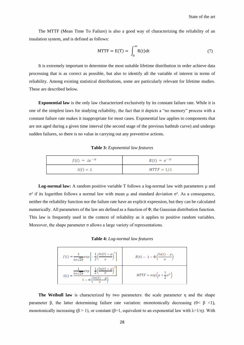
State of the art
28
The MTTF (Mean Time To Failure) is also a good way of characterizing the reliability of an
insulation system, and is defined as follows:
MTTF = E(T) = ∫ R(t)dt∞
0
(7)
It is extremely important to determine the most suitable lifetime distribution in order achieve data
processing that is as correct as possible, but also to identify all the variable of interest in terms of
reliability. Among existing statistical distributions, some are particularly relevant for lifetime studies.
These are described below.
Exponential law is the only law characterized exclusively by its constant failure rate. While it is
one of the simplest laws for studying reliability, the fact that it depicts a “no memory” process with a
constant failure rate makes it inappropriate for most cases. Exponential law applies to components that
are not aged during a given time interval (the second stage of the previous bathtub curve) and undergo
sudden failures, so there is no value in carrying out any preventive actions.
Table 3: Exponential law features
Log-normal law: A random positive variable T follows a log-normal law with parameters µ and
σ² if its logarithm follows a normal law with mean µ and standard deviation σ². As a consequence,
neither the reliability function nor the failure rate have an explicit expression, but they can be calculated
numerically. All parameters of the law are defined as a function of Φ, the Gaussian distribution function.
This law is frequently used in the context of reliability as it applies to positive random variables.
Moreover, the shape parameter σ allows a large variety of representations.
Table 4: Log-normal law features
The Weibull law is characterized by two parameters: the scale parameter η and the shape
parameter β, the latter determining failure rate variation: monotonically decreasing (0< β <1),
monotonically increasing (β > 1), or constant (β=1, equivalent to an exponential law with λ=1/η). With
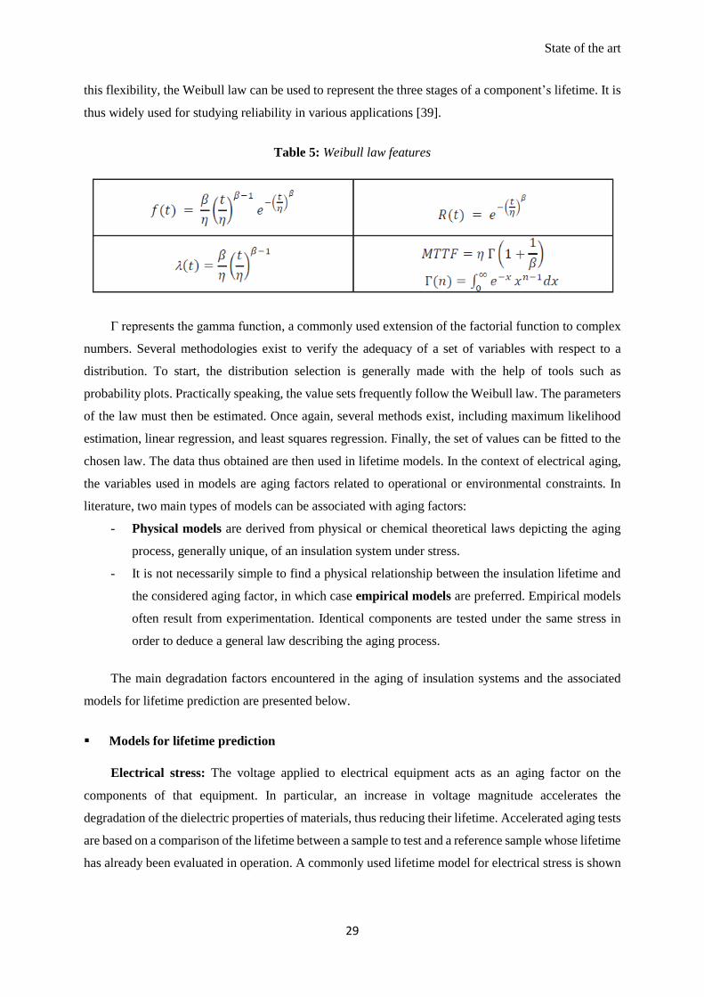
State of the art
29
this flexibility, the Weibull law can be used to represent the three stages of a component’s lifetime. It is
thus widely used for studying reliability in various applications [39].
Table 5: Weibull law features
Γ represents the gamma function, a commonly used extension of the factorial function to complex
numbers. Several methodologies exist to verify the adequacy of a set of variables with respect to a
distribution. To start, the distribution selection is generally made with the help of tools such as
probability plots. Practically speaking, the value sets frequently follow the Weibull law. The parameters
of the law must then be estimated. Once again, several methods exist, including maximum likelihood
estimation, linear regression, and least squares regression. Finally, the set of values can be fitted to the
chosen law. The data thus obtained are then used in lifetime models. In the context of electrical aging,
the variables used in models are aging factors related to operational or environmental constraints. In
literature, two main types of models can be associated with aging factors:
- Physical models are derived from physical or chemical theoretical laws depicting the aging
process, generally unique, of an insulation system under stress.
- It is not necessarily simple to find a physical relationship between the insulation lifetime and
the considered aging factor, in which case empirical models are preferred. Empirical models
often result from experimentation. Identical components are tested under the same stress in
order to deduce a general law describing the aging process.
The main degradation factors encountered in the aging of insulation systems and the associated
models for lifetime prediction are presented below.
Models for lifetime prediction
Electrical stress: The voltage applied to electrical equipment acts as an aging factor on the
components of that equipment. In particular, an increase in voltage magnitude accelerates the
degradation of the dielectric properties of materials, thus reducing their lifetime. Accelerated aging tests
are based on a comparison of the lifetime between a sample to test and a reference sample whose lifetime
has already been evaluated in operation. A commonly used lifetime model for electrical stress is shown
State of the art
30
below, where n represents the voltage endurance coefficient, L the lifetime, U the applied peak voltage
and, k a constant. The voltage endurance coefficient is the slope of the regression line.
L = kU−n (8)
The inverse power law is empirical. It supposes that the lifetime of a system varies inversely with
the level of applied stress. This is a very standard model associated with electrical stress in the presence
of PDs and applied to numerous components, including insulation systems.
Thermal stress: Temperature is a major aging factor in the context of electrical engineering.
Generally speaking, the performance of a component degrades quickly at high temperatures. The
thermal aging process can be described by the Arrhenius law, which expresses lifetime as an exponential
function of the inverse of temperature. L represents the lifetime, T the temperature (in Kelvin), and A
and b two constant parameters to estimate [38].
L = AebT
(9)
The Arrhenius law enables us to describe the speed variation of a chemical reaction as a function
of temperature. As an empirical law, it has been verified experimentally for a large number of reactions.
However, not all reactions follow this law.
The combined effect of thermal stress T and electrical stress E is often modelled by the generalized
Eyring law [40]. It is also possible to take into account any non-thermal stress by adding (Bi + Ci/T)
terms inside the exponential function.
L =A
Tne
bT
+(B+CT
)E (10)
Mechanical stress: Materials embedded in machines suffer constant mechanical stresses resulting
from vibrations or mechanical shocks. Vibrations are characterized by repetitive constraints of low
amplitude over a large number of cycles. In contrast, shocks are usually generated by larger accelerations
of shorter duration. Those two types of stresses lead to the degradation of materials’ physical properties,
including deformation and breakdown. Just like electrical stress, the effect of mechanical stress can be
modeled by an inverse power law (S being the value of the mechanical stress).
L =A
Sn (11)
It must be noted that other simple empirical laws exist and can be used to estimate the lifetime of
insulation materials. These laws are built mainly on tension-compression tests performed on steel and
extrapolated to other materials. The Wöhler curve, which represents the experimental relation between
stress amplitude and the number of cycles, is one of many examples of these other models.
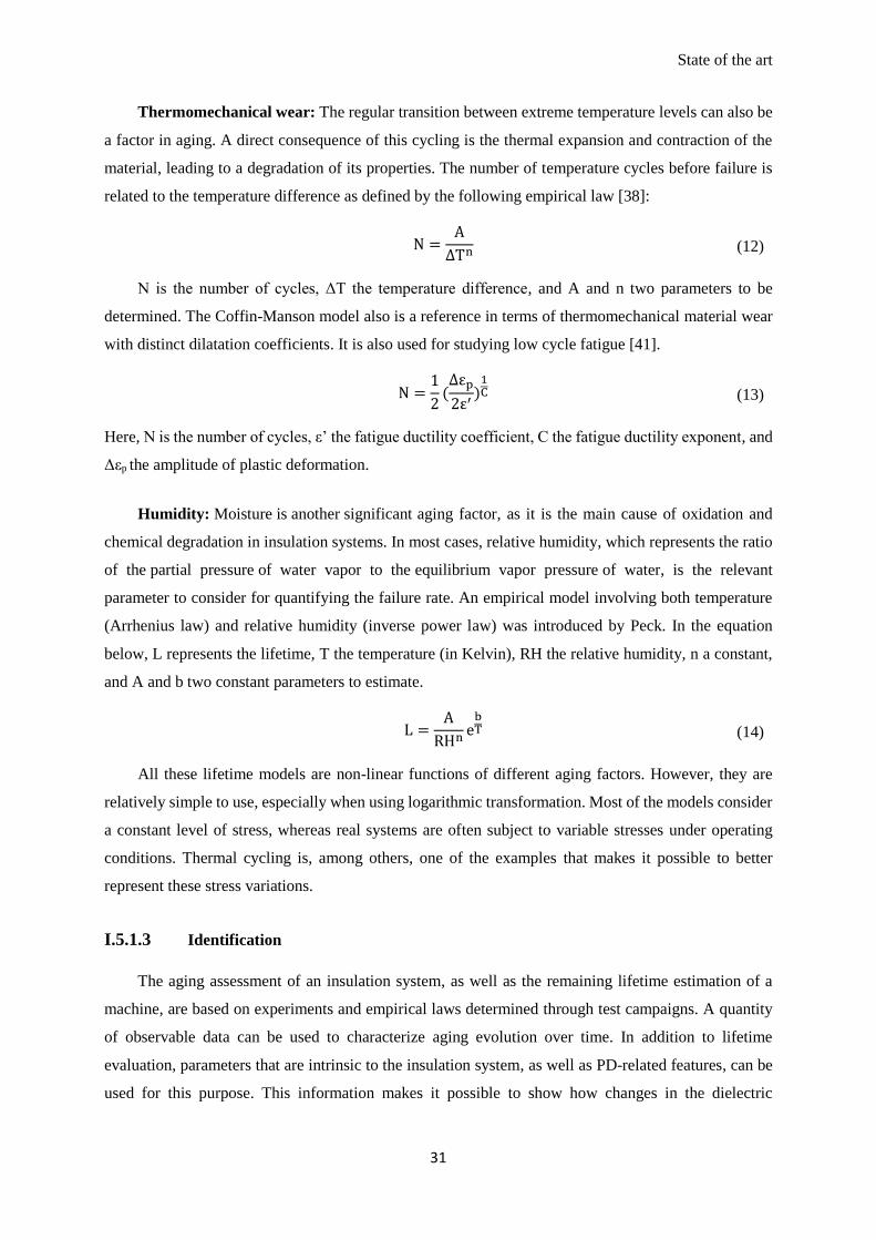
State of the art
31
Thermomechanical wear: The regular transition between extreme temperature levels can also be
a factor in aging. A direct consequence of this cycling is the thermal expansion and contraction of the
material, leading to a degradation of its properties. The number of temperature cycles before failure is
related to the temperature difference as defined by the following empirical law [38]:
N =A
∆Tn (12)
N is the number of cycles, ΔT the temperature difference, and A and n two parameters to be
determined. The Coffin-Manson model also is a reference in terms of thermomechanical material wear
with distinct dilatation coefficients. It is also used for studying low cycle fatigue [41].
N =1
2(∆εp
2ε′)
1C (13)
Here, N is the number of cycles, ε’ the fatigue ductility coefficient, C the fatigue ductility exponent, and
Δεp the amplitude of plastic deformation.
Humidity: Moisture is another significant aging factor, as it is the main cause of oxidation and
chemical degradation in insulation systems. In most cases, relative humidity, which represents the ratio
of the partial pressure of water vapor to the equilibrium vapor pressure of water, is the relevant
parameter to consider for quantifying the failure rate. An empirical model involving both temperature
(Arrhenius law) and relative humidity (inverse power law) was introduced by Peck. In the equation
below, L represents the lifetime, T the temperature (in Kelvin), RH the relative humidity, n a constant,
and A and b two constant parameters to estimate.
L =A
RHne
bT (14)
All these lifetime models are non-linear functions of different aging factors. However, they are
relatively simple to use, especially when using logarithmic transformation. Most of the models consider
a constant level of stress, whereas real systems are often subject to variable stresses under operating
conditions. Thermal cycling is, among others, one of the examples that makes it possible to better
represent these stress variations.
I.5.1.3 Identification
The aging assessment of an insulation system, as well as the remaining lifetime estimation of a
machine, are based on experiments and empirical laws determined through test campaigns. A quantity
of observable data can be used to characterize aging evolution over time. In addition to lifetime
evaluation, parameters that are intrinsic to the insulation system, as well as PD-related features, can be
used for this purpose. This information makes it possible to show how changes in the dielectric
State of the art
32
properties of materials take place, and above all how to relate those changes with applied stress and
material aging.
Dielectric properties of materials
Insulation resistance measurement during aging cycles is one of the main indicators of both the
insulation condition and the speed of degradation. An insulation system has opposite characteristics to
those of a conductor, namely it resists the flow of current when voltage is applied to system terminals.
The better the insulation, the higher the insulation resistance, and the better its ability to maintain high
resistance over time. As there is no such thing as “perfect insulation”, a leakage current is always present
and leads to a decrease in this resistance (see Figure I-24). Measurement at regular intervals is thus an
effective way to assess insulation integrity.
Figure I-24: Insulation resistance measurement results after 1 minute [42]
This measurement method is the simplest, but it is strongly affected by temperature and humidity.
Other methods exist that allow normalizing measurements and taking into account the influence of the
time of application, such as the Polarization Index (PI) or the Dielectric Absorption Ratio (DAR).
Dielectric permittivity is a physical property describing the response of a given dielectric to an
electrical field. At the microscopic scale, permittivity is related to the electrical polarizability of
molecules comprising the material. It is a tensor quantity that can become a scalar in an isotropic
material. It is generally a complex number, with the imaginary part representing electric field absorption
or emission phenomena. Dielectric loss quantifies a dielectric material’s inherent dissipation of
electromagnetic energy. It can be parameterized in terms of either the loss angle δ or the
corresponding loss tangent tan δ. Both refer to the phasor in the complex plane whose real and
imaginary parts are the resistive component of an electromagnetic field and its reactive counterpart.
These losses can be taken into account by defining complex permittivity:
ε∗ = ε′ − iε′′ (15)
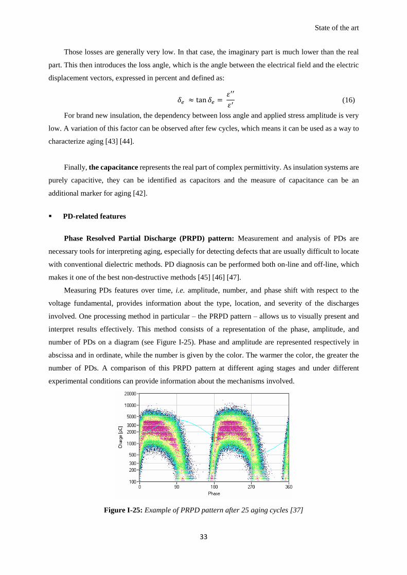
State of the art
33
Those losses are generally very low. In that case, the imaginary part is much lower than the real
part. This then introduces the loss angle, which is the angle between the electrical field and the electric
displacement vectors, expressed in percent and defined as:
𝛿𝑒 ≈ tan 𝛿𝑒 = 휀′′
휀′ (16)
For brand new insulation, the dependency between loss angle and applied stress amplitude is very
low. A variation of this factor can be observed after few cycles, which means it can be used as a way to
characterize aging [43] [44].
Finally, the capacitance represents the real part of complex permittivity. As insulation systems are
purely capacitive, they can be identified as capacitors and the measure of capacitance can be an
additional marker for aging [42].
PD-related features
Phase Resolved Partial Discharge (PRPD) pattern: Measurement and analysis of PDs are
necessary tools for interpreting aging, especially for detecting defects that are usually difficult to locate
with conventional dielectric methods. PD diagnosis can be performed both on-line and off-line, which
makes it one of the best non-destructive methods [45] [46] [47].
Measuring PDs features over time, i.e. amplitude, number, and phase shift with respect to the
voltage fundamental, provides information about the type, location, and severity of the discharges
involved. One processing method in particular – the PRPD pattern – allows us to visually present and
interpret results effectively. This method consists of a representation of the phase, amplitude, and
number of PDs on a diagram (see Figure I-25). Phase and amplitude are represented respectively in
abscissa and in ordinate, while the number is given by the color. The warmer the color, the greater the
number of PDs. A comparison of this PRPD pattern at different aging stages and under different
experimental conditions can provide information about the mechanisms involved.
Figure I-25: Example of PRPD pattern after 25 aging cycles [37]
State of the art
34
PDIV (Partial Discharge Inception Voltage) can also indirectly be considered as an aging
marker. Indeed, PDIV varies depending on a number of parameters such as environment, temperature,
and evolution of the EIS properties over time, and thus enables us to obtain a snapshot of the insulation
system. PDIV is assumed to be independent of the frequency but strongly dependent on the condition
of insulation. The more advanced the aging, the lower the insulation thickness, and the greater the PDIV.
It is important to keep in mind that the partial discharge phenomenon is more a symptom of degradation
than a default itself; PDIV and its evolution over time thus characterizes the aging associated with those
symptoms.
Finally, measurement of the discharge energy is the last major aging indicator [48]. Partial
discharges dissipate energy in different forms:
- Electromagnetic emissions (radio waves, light, heat)
- Acoustic emissions (into the audible and ultrasonic ranges)
- Gas emissions (including ozone and nitrogen oxides)
One of the most commonly used methods for measuring the energy associated with PDs is the
Lissajous method, which consists of plotting the charges transferred through the gas against the applied
voltage. The dissipated energy during one cycle can then be calculated from the Lissajous curve. P
represents the electric power, and integration is calculated on one period of time.
𝐸 = P ∗ T = ∫ V(t)dq (17)
The dissipated energy corresponds to the area under the Lissajous curve. This energy varies
strongly with the aging time and conditions and can also give information about the aging process, or
even allow comparing different operating points. This method has been proven for a sinusoidal voltage
supply, but still needs to be improved for square wave voltages, primarily because of the difficulty in
measuring the effective charge associated with PDs.
There is a long list of diagnosis and aging evaluation methods, as well as aging indicators. For the
sake of brevity here, only the most commonly used ones, both during operation or by interrupting the
aging, were presented [49] [50].
The direct consequence of the continued presence of degradation phenomena over time is EIS
aging. The manifestations of this aging are numerous. They depend on the applied stresses and are
expressed in different ways, through the variation of different parameters. In order to best identify aging
mechanisms, from cause to effect, the next subsection describes aging as it takes places in electrical
machines and, more specifically, discusses the influence of the main electrical and environmental
constraints on PD features and aging, as well as their interactions. As a second step, the following
subsection points out on one hand the interest and necessity of reproducing this aging on samples, and
on the other hand, the procedures and strategies for conducting these accelerated aging tests.
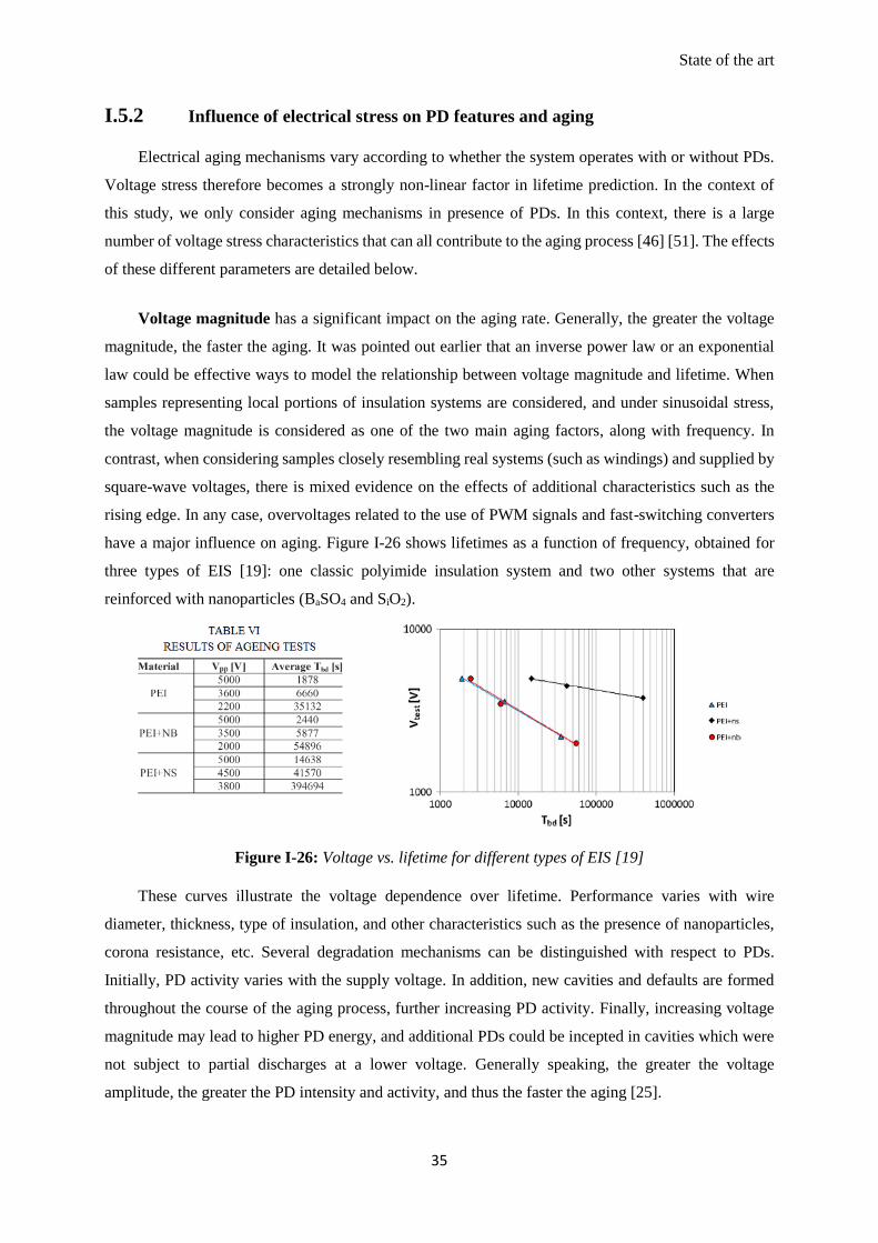
State of the art
35
I.5.2 Influence of electrical stress on PD features and aging
Electrical aging mechanisms vary according to whether the system operates with or without PDs.
Voltage stress therefore becomes a strongly non-linear factor in lifetime prediction. In the context of
this study, we only consider aging mechanisms in presence of PDs. In this context, there is a large
number of voltage stress characteristics that can all contribute to the aging process [46] [51]. The effects
of these different parameters are detailed below.
Voltage magnitude has a significant impact on the aging rate. Generally, the greater the voltage
magnitude, the faster the aging. It was pointed out earlier that an inverse power law or an exponential
law could be effective ways to model the relationship between voltage magnitude and lifetime. When
samples representing local portions of insulation systems are considered, and under sinusoidal stress,
the voltage magnitude is considered as one of the two main aging factors, along with frequency. In
contrast, when considering samples closely resembling real systems (such as windings) and supplied by
square-wave voltages, there is mixed evidence on the effects of additional characteristics such as the
rising edge. In any case, overvoltages related to the use of PWM signals and fast-switching converters
have a major influence on aging. Figure I-26 shows lifetimes as a function of frequency, obtained for
three types of EIS [19]: one classic polyimide insulation system and two other systems that are
reinforced with nanoparticles (BaSO4 and SiO2).
Figure I-26: Voltage vs. lifetime for different types of EIS [19]
These curves illustrate the voltage dependence over lifetime. Performance varies with wire
diameter, thickness, type of insulation, and other characteristics such as the presence of nanoparticles,
corona resistance, etc. Several degradation mechanisms can be distinguished with respect to PDs.
Initially, PD activity varies with the supply voltage. In addition, new cavities and defaults are formed
throughout the course of the aging process, further increasing PD activity. Finally, increasing voltage
magnitude may lead to higher PD energy, and additional PDs could be incepted in cavities which were
not subject to partial discharges at a lower voltage. Generally speaking, the greater the voltage
amplitude, the greater the PD intensity and activity, and thus the faster the aging [25].
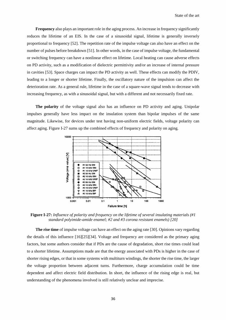
State of the art
36
Frequency also plays an important role in the aging process. An increase in frequency significantly
reduces the lifetime of an EIS. In the case of a sinusoidal signal, lifetime is generally inversely
proportional to frequency [52]. The repetition rate of the impulse voltage can also have an effect on the
number of pulses before breakdown [51]. In other words, in the case of impulse voltage, the fundamental
or switching frequency can have a nonlinear effect on lifetime. Local heating can cause adverse effects
on PD activity, such as a modification of dielectric permittivity and/or an increase of internal pressure
in cavities [53]. Space charges can impact the PD activity as well. These effects can modify the PDIV,
leading to a longer or shorter lifetime. Finally, the oscillatory nature of the impulsion can affect the
deterioration rate. As a general rule, lifetime in the case of a square-wave signal tends to decrease with
increasing frequency, as with a sinusoidal signal, but with a different and not necessarily fixed rate.
The polarity of the voltage signal also has an influence on PD activity and aging. Unipolar
impulses generally have less impact on the insulation system than bipolar impulses of the same
magnitude. Likewise, for devices under test having non-uniform electric fields, voltage polarity can
affect aging. Figure I-27 sums up the combined effects of frequency and polarity on aging.
Figure I-27: Influence of polarity and frequency on the lifetime of several insulating materials (#1
standard polyimide-amide enamel; #2 and #3 corona resistant enamels) [20]
The rise time of impulse voltage can have an effect on the aging rate [30]. Opinions vary regarding
the details of this influence [16][25][34]. Voltage and frequency are considered as the primary aging
factors, but some authors consider that if PDs are the cause of degradation, short rise times could lead
to a shorter lifetime. Assumptions made are that the energy associated with PDs is higher in the case of
shorter rising edges, or that in some systems with multiturn windings, the shorter the rise time, the larger
the voltage proportion between adjacent turns. Furthermore, charge accumulation could be time
dependent and affect electric field distribution. In short, the influence of the rising edge is real, but
understanding of the phenomena involved is still relatively unclear and imprecise.
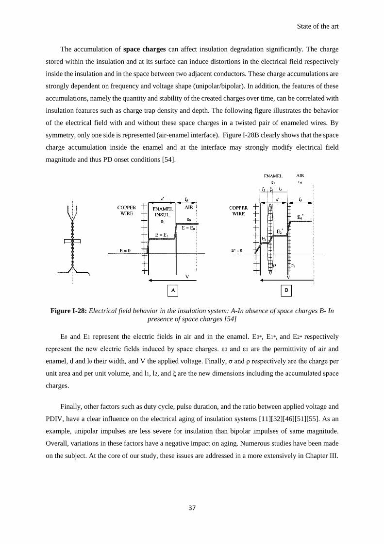
State of the art
37
The accumulation of space charges can affect insulation degradation significantly. The charge
stored within the insulation and at its surface can induce distortions in the electrical field respectively
inside the insulation and in the space between two adjacent conductors. These charge accumulations are
strongly dependent on frequency and voltage shape (unipolar/bipolar). In addition, the features of these
accumulations, namely the quantity and stability of the created charges over time, can be correlated with
insulation features such as charge trap density and depth. The following figure illustrates the behavior
of the electrical field with and without these space charges in a twisted pair of enameled wires. By
symmetry, only one side is represented (air-enamel interface). Figure I-28B clearly shows that the space
charge accumulation inside the enamel and at the interface may strongly modify electrical field
magnitude and thus PD onset conditions [54].
Figure I-28: Electrical field behavior in the insulation system: A-In absence of space charges B- In
presence of space charges [54]
E0 and E1 represent the electric fields in air and in the enamel. E0*, E1*, and E2* respectively
represent the new electric fields induced by space charges. ε0 and ε1 are the permittivity of air and
enamel, d and l0 their width, and V the applied voltage. Finally, σ and ρ respectively are the charge per
unit area and per unit volume, and l1, l2, and ξ are the new dimensions including the accumulated space
charges.
Finally, other factors such as duty cycle, pulse duration, and the ratio between applied voltage and
PDIV, have a clear influence on the electrical aging of insulation systems [11][32][46][51][55]. As an
example, unipolar impulses are less severe for insulation than bipolar impulses of same magnitude.
Overall, variations in these factors have a negative impact on aging. Numerous studies have been made
on the subject. At the core of our study, these issues are addressed in a more extensively in Chapter III.
State of the art
38
I.5.3 Environmental influence on PD features and aging
I.5.3.1 Thermal aging
The increase of ohmic, magnetic, and dielectric losses inside machines can lead to insulation
heating. This phenomenon is linked to PDs to the extent that insulation heating causes a modification of
its characteristic parameters (permittivity, geometry, conductivity, PDIV) and, in turn, greatly modifies
field distribution and the insulation’s resilience to PDs.
Thermal stress consists largely of thermal agitation within the material and irreversible chemical
reactions. During normal machine operation, heating is mainly a result of Joule, eddy current, and
mechanical losses. Temperature, when constant, acts as a catalyst rather than actually degrading the
material itself. The degradation rate can be increased if dielectric losses are increased, in turn leading to
local enhancement of temperature in an area with high electrical stress. A temperature increase can also
lead to an increase in permittivity, causing higher electrical stress in adjacent cavities, lower PDIV, and
thus enhanced PD activity. Furthermore, it can have an influence on the gas pressure in closed cavities,
and on charge trapping and de-trapping times. In addition to the thermal energy gained by electrons,
higher temperature can lead to a reduction in relative air density, which is inversely proportional to the
mean free path. As a consequence, electrons must travel a longer distance between two collisions and
store more energy. This produces PDs that are more energetic and certainly more damaging for
insulation systems (Figure I-29).
When thermal cycles are imposed, degradation is referred to as thermomechanical aging [56]. This
aging type is primarily due to differences in the thermal dilatation coefficients between constituents and
the insulation system. These differences can create constraints which, in turn, may generate or expand
pre-existing delamination, and/or increase PD activity, amplitude, and repetition rate. These constraints
are enhanced by thermal cycling, as the temperature of materials does not vary at the same speed in that
case. In short, temperature acts as an indirect factor in aging by impacting many other parameters and
phenomena.
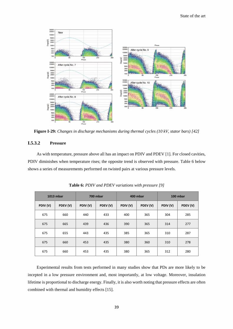
State of the art
39
Figure I-29: Changes in discharge mechanisms during thermal cycles (10 kV, stator bars) [42]
I.5.3.2 Pressure
As with temperature, pressure above all has an impact on PDIV and PDEV [1]. For closed cavities,
PDIV diminishes when temperature rises; the opposite trend is observed with pressure. Table 6 below
shows a series of measurements performed on twisted pairs at various pressure levels.
Table 6: PDIV and PDEV variations with pressure [9]
1013 mbar 700 mbar 400 mbar 100 mbar
PDIV (V) PDEV (V) PDIV (V) PDEV (V) PDIV (V) PDEV (V) PDIV (V) PDEV (V)
675 660 440 433 400 365 304 285
675 665 439 436 390 365 314 277
675 655 443 435 385 365 310 287
675 660 453 435 380 360 310 278
675 660 453 435 380 365 312 280
Experimental results from tests performed in many studies show that PDs are more likely to be
incepted in a low pressure environment and, most importantly, at low voltage. Moreover, insulation
lifetime is proportional to discharge energy. Finally, it is also worth noting that pressure effects are often
combined with thermal and humidity effects [15].
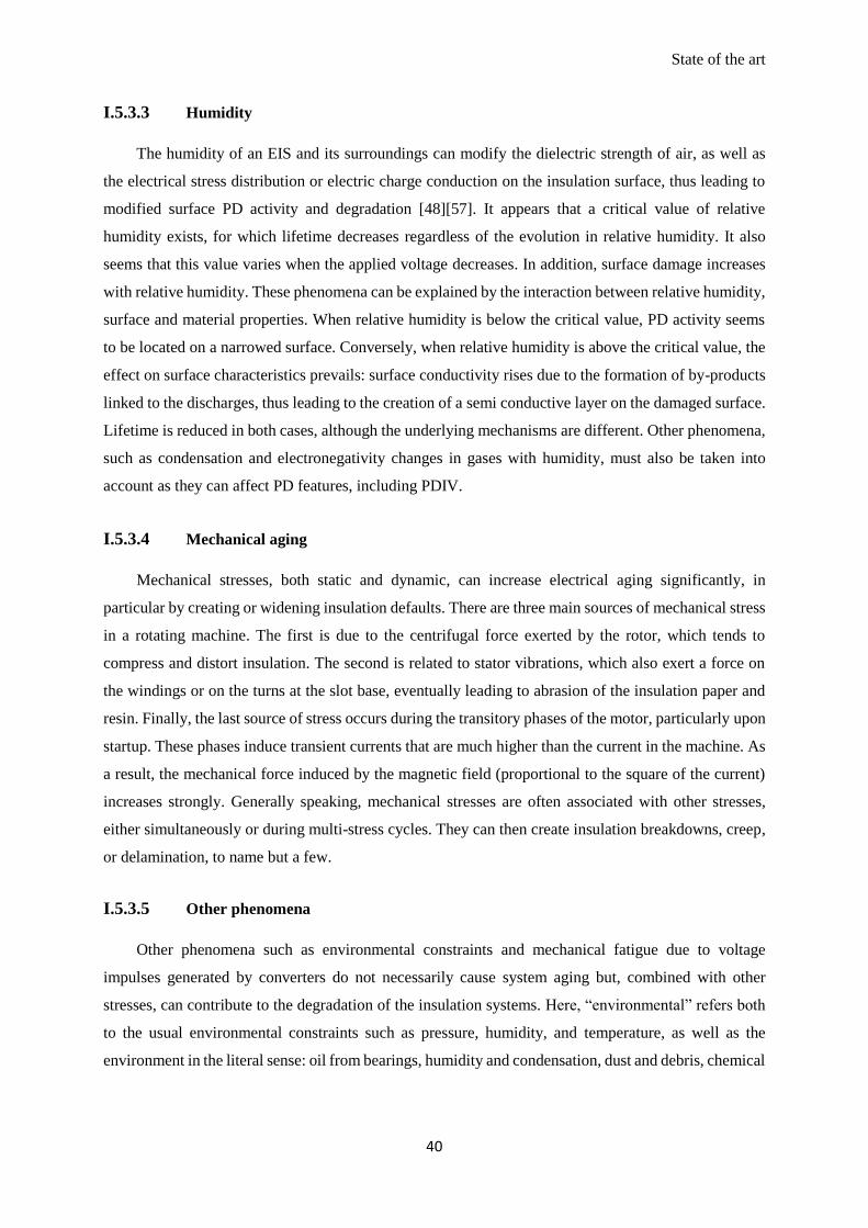
State of the art
40
I.5.3.3 Humidity
The humidity of an EIS and its surroundings can modify the dielectric strength of air, as well as
the electrical stress distribution or electric charge conduction on the insulation surface, thus leading to
modified surface PD activity and degradation [48][57]. It appears that a critical value of relative
humidity exists, for which lifetime decreases regardless of the evolution in relative humidity. It also
seems that this value varies when the applied voltage decreases. In addition, surface damage increases
with relative humidity. These phenomena can be explained by the interaction between relative humidity,
surface and material properties. When relative humidity is below the critical value, PD activity seems
to be located on a narrowed surface. Conversely, when relative humidity is above the critical value, the
effect on surface characteristics prevails: surface conductivity rises due to the formation of by-products
linked to the discharges, thus leading to the creation of a semi conductive layer on the damaged surface.
Lifetime is reduced in both cases, although the underlying mechanisms are different. Other phenomena,
such as condensation and electronegativity changes in gases with humidity, must also be taken into
account as they can affect PD features, including PDIV.
I.5.3.4 Mechanical aging
Mechanical stresses, both static and dynamic, can increase electrical aging significantly, in
particular by creating or widening insulation defaults. There are three main sources of mechanical stress
in a rotating machine. The first is due to the centrifugal force exerted by the rotor, which tends to
compress and distort insulation. The second is related to stator vibrations, which also exert a force on
the windings or on the turns at the slot base, eventually leading to abrasion of the insulation paper and
resin. Finally, the last source of stress occurs during the transitory phases of the motor, particularly upon
startup. These phases induce transient currents that are much higher than the current in the machine. As
a result, the mechanical force induced by the magnetic field (proportional to the square of the current)
increases strongly. Generally speaking, mechanical stresses are often associated with other stresses,
either simultaneously or during multi-stress cycles. They can then create insulation breakdowns, creep,
or delamination, to name but a few.
I.5.3.5 Other phenomena
Other phenomena such as environmental constraints and mechanical fatigue due to voltage
impulses generated by converters do not necessarily cause system aging but, combined with other
stresses, can contribute to the degradation of the insulation systems. Here, “environmental” refers both
to the usual environmental constraints such as pressure, humidity, and temperature, as well as the
environment in the literal sense: oil from bearings, humidity and condensation, dust and debris, chemical
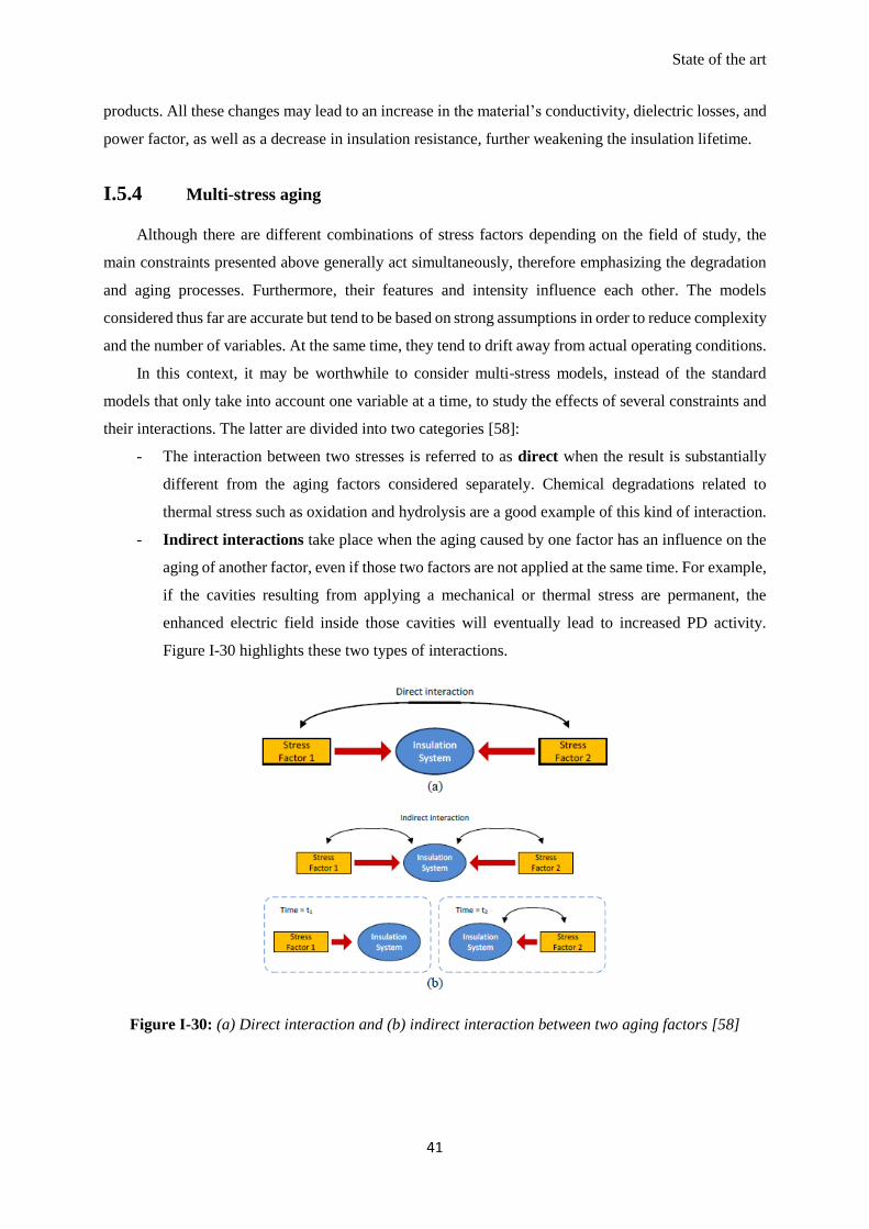
State of the art
41
products. All these changes may lead to an increase in the material’s conductivity, dielectric losses, and
power factor, as well as a decrease in insulation resistance, further weakening the insulation lifetime.
I.5.4 Multi-stress aging
Although there are different combinations of stress factors depending on the field of study, the
main constraints presented above generally act simultaneously, therefore emphasizing the degradation
and aging processes. Furthermore, their features and intensity influence each other. The models
considered thus far are accurate but tend to be based on strong assumptions in order to reduce complexity
and the number of variables. At the same time, they tend to drift away from actual operating conditions.
In this context, it may be worthwhile to consider multi-stress models, instead of the standard
models that only take into account one variable at a time, to study the effects of several constraints and
their interactions. The latter are divided into two categories [58]:
- The interaction between two stresses is referred to as direct when the result is substantially
different from the aging factors considered separately. Chemical degradations related to
thermal stress such as oxidation and hydrolysis are a good example of this kind of interaction.
- Indirect interactions take place when the aging caused by one factor has an influence on the
aging of another factor, even if those two factors are not applied at the same time. For example,
if the cavities resulting from applying a mechanical or thermal stress are permanent, the
enhanced electric field inside those cavities will eventually lead to increased PD activity.
Figure I-30 highlights these two types of interactions.
Figure I-30: (a) Direct interaction and (b) indirect interaction between two aging factors [58]
State of the art
42
One of the cons of the multi-stress method is that it can be difficult to determine which constraint
specifically affected aging. However, it allows highlight combined aging mechanisms that are likely to
occur under real operating conditions.
In terms of experiments, it is quite costly and challenging to consider multi-stress models involving
all the parameters related to the aging process. Statistical methods considering only a restricted number
of variables thus exist to model lifetimes and answer the following important questions:
- What are the most influential factors?
- Are there any interactions between those factors?
- Is it possible to linearize the process as a function of those factors, and is the obtained model
predictive?
- How can we minimize the number of experiments to make while ensuring the maximum
amount of information?
- Is there any bias in measurement results?
Design Of Experiments (DoE) is one of many methods that make it possible to answer these
questions, and it can be applied for various processes [59]. DoE consists of an ordered series of tests
aiming to determine – with the lowest possible number of tests and the maximum level of precision –
the influence of various parameters for optimizing cost and/or performance.
To date, most aging models and experiments consider variables separately. Modeling the lifetime
of insulation systems when considering several stresses simultaneously is therefore a further step
towards understanding the influence of a whole set of parameters and their interactions on any given
phenomenon. Some studies take this problem very seriously and already propose multi-stress models
[58][60][61]. With respect to multi-stress aging in the form of cycles, these models also make it possible
to study the influence of combined stresses, but rather in terms of indirect interactions. The latter are
generally preferred in the industry.
State of the art
43
I.6 Conclusion
The issues of partial discharges and aging mechanisms of insulation systems used in rotating
machines were addressed throughout this chapter. A state of the art of the degradation mechanisms and
the systems on which they appear was presented. The influence of electrical stress and control strategy
on aging was reviewed in detail and, finally, the aging phenomenon itself was defined and illustrated.
Insulation system aging is a common issue in a number of areas, in particular with the expanding
use of electrical energy. Despite different challenges and structures, the phenomena involved are similar:
mainly PDs and their consequences on insulation systems. These systems may be designed to react
differently to these discharges, but in any case, PD presence is an issue that affects the reliability of the
entire electromechanical chain.
This is particularly true due to the fact the converters used to supply these machines have a specific
design that leads to the generation of very harmful stresses at the motor terminals. Moreover, the
transition from conventional silicon-based components to new wide bandgap components only makes
matters worse.
The aging of insulation systems is the direct consequence of these severe new constraints.
Modeling, identification, and reproduction of this aging are thus key aspects for understanding
degradation mechanisms, and potentially preventing and predicting the effects of aging.
Analysis of partial discharge influence in an electromechanical chain using fast switching inverters
can be divided into three steps:
- Identification of the electrical stresses as seen by the machine
- Influence of these constraints on PD activity
- Consequences of these PDs in terms of aging
The first of these steps is discussed in the next chapter. The state of the art presented above is
intended to provide a general overview of aging issues regardless of the type of machine considered.
From this point forward, our work focuses more specifically on the railway context (Type II machines).
Nonetheless, the parallel with low voltage machines will remain a recurrent thread of this study.

Electrical stress identification
45
Chapter II. Electrical stress identification
II.1 Purpose of the study
An important step in studying the reliability of insulation systems is the characterization of
electrical stresses. More particularly, clear insight regarding the distribution of electrical stresses to
which the machine is subject is a first step towards the systematic determination of the conditions of
occurrence for partial discharges, as well as their consequences on insulation system lifetime.
Numerous studies have been made on the subject of low voltage machines [62][63][64][65][66].
However, studies concerning high voltage machines are more rare or outdated. It is thus necessary to
have insight into electrical constraint mapping in the motor – more specifically on the turn-to-turn,
phase-to-ground, and phase-to-phase insulation systems – in order to be able to reproduce those
constraints on samples but also to understand the aging process as a whole from PD ignition to
breakdown.
With that in mind, the following part of this work seeks to perform thorough electrical stress
mapping depending on both geometric and electrical parameters. The final objective is to establish a
comparison between the electrical stresses generated by Si IGBT-based and SiC MOSFET-based
inverters. A series of measurements of turn-to-turn, phase-to-ground, and phase-to-phase stresses was
performed with different configurations and in accordance with a detailed test plan previously
established based on preliminary tests.
The experimental setup overall, as well as the results of the test campaign and analysis are
presented below. In addition, partial discharge measurements are performed to complement these results
and achieve insight into not only the severity of the stresses but also their impact in terms of PDs.
II.2 Experimental setup
The electrical stresses at motor terminals depend on multiple parameters, both geometric and
electric. In particular, inverters using SiC-based components enable the generation of dV/dt much higher
than the usual levels provided by Si-based inverters. Furthermore, these stresses differ vastly depending
on the insulation system and are altered throughout their propagation in winding. In order to perform
thorough electrical stress mapping, it is important to control many parameters and to have access to
multiple locations in the motor. To carry out this task, we built an experimental test bench. The objective
is to characterize the influence of those parameters on equipment insulation, and consequently to
understand the extent to which PD activity is affected, by identifying voltage distribution in the winding
(voltage increase between turns, phase-to-ground…) of a type II machine.
Electrical stress identification
46
II.2.1 Description of the power chain
A voltage source supplies the chain with a DC bus. This voltage is then filtered and converted using
an inverter driven by a control device. This converted voltage goes through cables and finally supplies
an asynchronous formed wound motor equipped to provide access to particular points in the motor. A
general bench description and a series of photos of the electromechanical chain are given in Figure II-1.
(a)
(b)
Figure II-1: General description (a) and photos (b) of the experimental test bench configured for
characterizing voltage constraints on insulation
Electrical stress identification
47
More specifically, a controller allows for the transmission of information to the inverters and thus
the adjustment of parameters such as DC bus voltage, torque, and rotation speed of the motor. Sensors
are placed all along the electromechanical chain to gather information regarding system operation.
Therefore, information flows bidirectionally between the controller and inverter. Several inverters are
used in this study. The two main inverters, which are designated in this document as inverters A and B,
have a similar structure but different power modules, enabling the comparison of Si IGBT and SiC
MOSFET technologies. A third inverter (referred to as inverter C) also uses SiC MOSFET technology,
but with higher performance in terms of switching speed. Finally, two additional inverters (respectively
inverters D and E) were studied to a lesser extent and only allow comparison at a larger scale for some
parameters. It must be noted that inverters A and B are expected to operate at a higher DC bus voltage
than inverters C, D, and E. Table 7 provides a brief summary of performance with the values of the
maximum voltage slope (in kV/µs) for each inverter. These values were obtained based on voltage
measurements performed at each inverter output. For all inverters, simplified designations are provided
and will be used later for the sake of clarity.
Table 7: Maximum rising edge at the inverter output for all technologies
Inverter name Technology Maximum rising edge (kV/µs)
A Si IGBT 4.43
B SiC MOSFET 8.17
C SiC MOSFET 23.26
D Si IGBT 1.29
E SiC MOSFET 8.07
Two types of input voltages are considered in this study. The inverters can be controlled by means
of a double pulse as voltage input by operating two of the inverter legs simultaneously, while the last
leg is either disconnected or set to an off state. It is also possible to use PWM signals that were specially
designed to ensure that the switched current range is as large as possible. (Figure II-2). The first type of
input voltage is much simpler to set up and makes it possible to overcome operating constraints (the
machine is not running) to focus on electrical stress only. For the second type, the interest is to reproduce
the machine’s operating environment. It must be noted that most tests were performed using PWM
signals, as the purpose of the study is to identify electrical stresses inside the machine under operating
conditions. With respect to the earthing (grounding) system, the motor as well as the -HV source (Figure
II-2) on the inverter side are grounded locally. Normatively speaking, the considered earthing system is
a TT network.
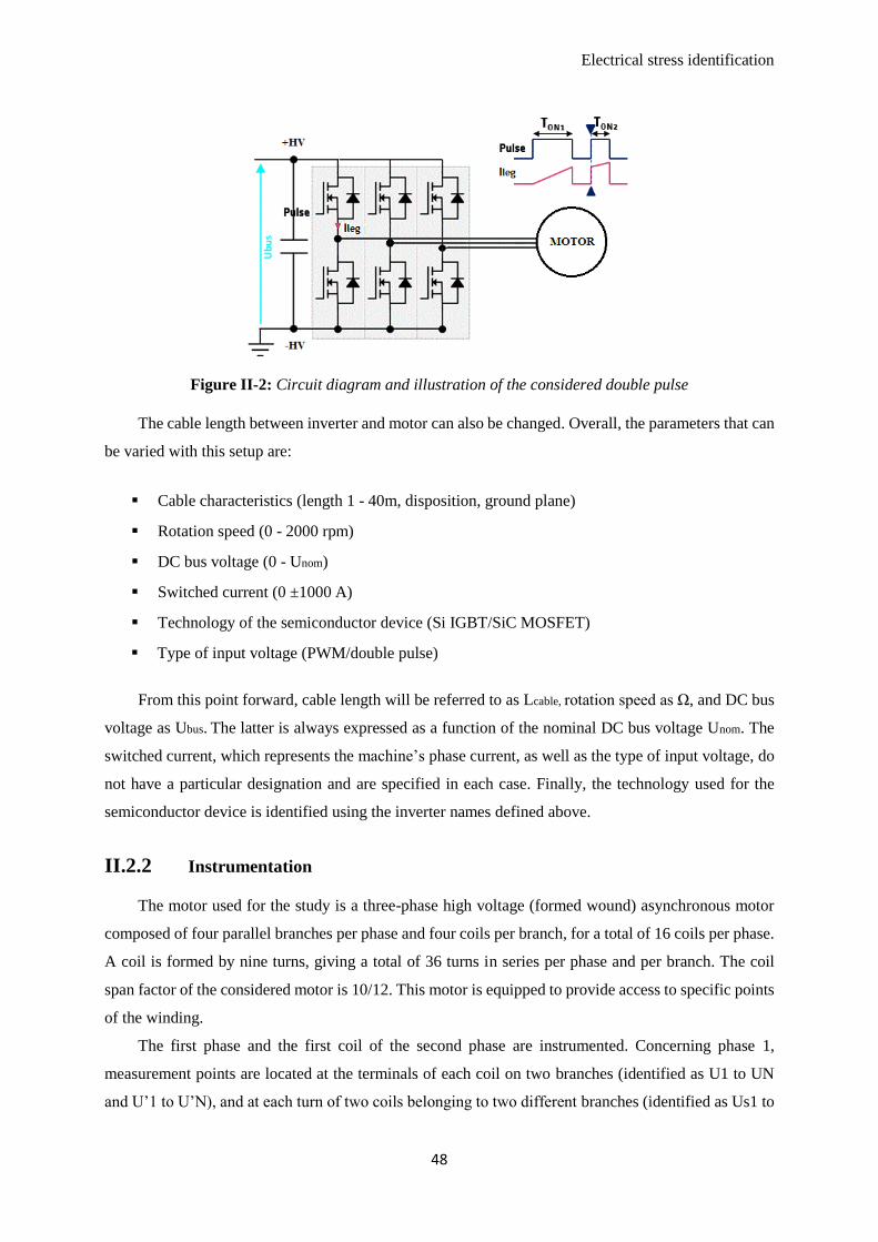
Electrical stress identification
48
Figure II-2: Circuit diagram and illustration of the considered double pulse
The cable length between inverter and motor can also be changed. Overall, the parameters that can
be varied with this setup are:
Cable characteristics (length 1 - 40m, disposition, ground plane)
Rotation speed (0 - 2000 rpm)
DC bus voltage (0 - Unom)
Switched current (0 ±1000 A)
Technology of the semiconductor device (Si IGBT/SiC MOSFET)
Type of input voltage (PWM/double pulse)
From this point forward, cable length will be referred to as Lcable, rotation speed as Ω, and DC bus
voltage as Ubus. The latter is always expressed as a function of the nominal DC bus voltage Unom. The
switched current, which represents the machine’s phase current, as well as the type of input voltage, do
not have a particular designation and are specified in each case. Finally, the technology used for the
semiconductor device is identified using the inverter names defined above.
II.2.2 Instrumentation
The motor used for the study is a three-phase high voltage (formed wound) asynchronous motor
composed of four parallel branches per phase and four coils per branch, for a total of 16 coils per phase.
A coil is formed by nine turns, giving a total of 36 turns in series per phase and per branch. The coil
span factor of the considered motor is 10/12. This motor is equipped to provide access to specific points
of the winding.
The first phase and the first coil of the second phase are instrumented. Concerning phase 1,
measurement points are located at the terminals of each coil on two branches (identified as U1 to UN
and U’1 to U’N), and at each turn of two coils belonging to two different branches (identified as Us1 to
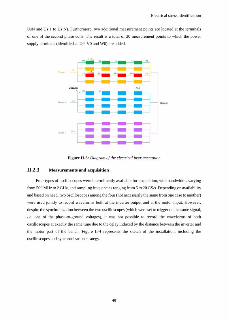
Electrical stress identification
49
UsN and Us’1 to Us’N). Furthermore, two additional measurement points are located at the terminals
of one of the second phase coils. The result is a total of 30 measurement points to which the power
supply terminals (identified as U0, V0 and W0) are added.
Figure II-3: Diagram of the electrical instrumentation
II.2.3 Measurements and acquisition
Four types of oscilloscopes were intermittently available for acquisition, with bandwidths varying
from 500 MHz to 2 GHz, and sampling frequencies ranging from 5 to 20 GS/s. Depending on availability
and based on need, two oscilloscopes among the four (not necessarily the same from one case to another)
were used jointly to record waveforms both at the inverter output and at the motor input. However,
despite the synchronization between the two oscilloscopes (which were set to trigger on the same signal,
i.e. one of the phase-to-ground voltages), it was not possible to record the waveforms of both
oscilloscopes at exactly the same time due to the delay induced by the distance between the inverter and
the motor part of the bench. Figure II-4 represents the sketch of the installation, including the
oscilloscopes and synchronization strategy.
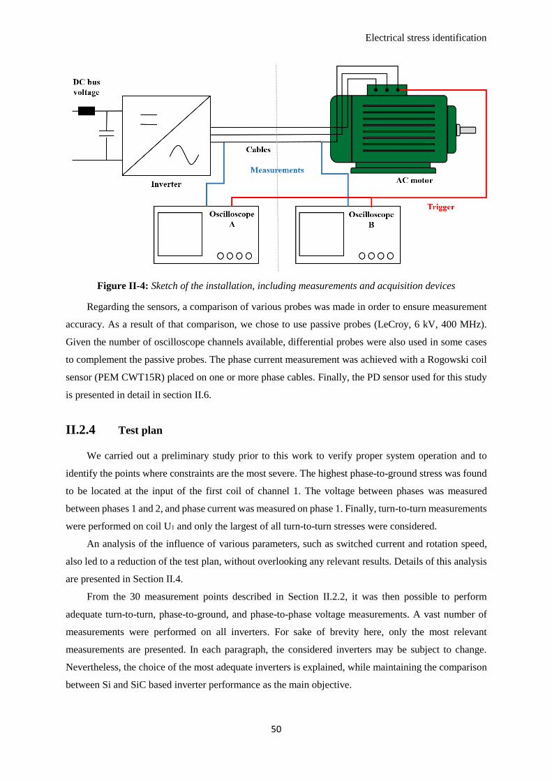
Electrical stress identification
50
Figure II-4: Sketch of the installation, including measurements and acquisition devices
Regarding the sensors, a comparison of various probes was made in order to ensure measurement
accuracy. As a result of that comparison, we chose to use passive probes (LeCroy, 6 kV, 400 MHz).
Given the number of oscilloscope channels available, differential probes were also used in some cases
to complement the passive probes. The phase current measurement was achieved with a Rogowski coil
sensor (PEM CWT15R) placed on one or more phase cables. Finally, the PD sensor used for this study
is presented in detail in section II.6.
II.2.4 Test plan
We carried out a preliminary study prior to this work to verify proper system operation and to
identify the points where constraints are the most severe. The highest phase-to-ground stress was found
to be located at the input of the first coil of channel 1. The voltage between phases was measured
between phases 1 and 2, and phase current was measured on phase 1. Finally, turn-to-turn measurements
were performed on coil U1 and only the largest of all turn-to-turn stresses were considered.
An analysis of the influence of various parameters, such as switched current and rotation speed,
also led to a reduction of the test plan, without overlooking any relevant results. Details of this analysis
are presented in Section II.4.
From the 30 measurement points described in Section II.2.2, it was then possible to perform
adequate turn-to-turn, phase-to-ground, and phase-to-phase voltage measurements. A vast number of
measurements were performed on all inverters. For sake of brevity here, only the most relevant
measurements are presented. In each paragraph, the considered inverters may be subject to change.
Nevertheless, the choice of the most adequate inverters is explained, while maintaining the comparison
between Si and SiC based inverter performance as the main objective.
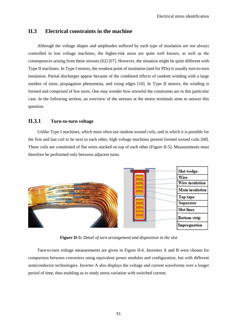
Electrical stress identification
51
II.3 Electrical constraints in the machine
Although the voltage shapes and amplitudes suffered by each type of insulation are not always
controlled in low voltage machines, the higher-risk areas are quite well known, as well as the
consequences arising from these stresses [62] [67]. However, the situation might be quite different with
Type II machines. In Type I motors, the weakest point of insulation (and for PDs) is usually turn-to-turn
insulation. Partial discharges appear because of the combined effects of random winding with a large
number of turns, propagation phenomena, and rising edges [10]. In Type II motors, the winding is
formed and comprised of few turns. One may wonder how stressful the constraints are in this particular
case. In the following section, an overview of the stresses at the motor terminals aims to answer this
question.
II.3.1 Turn-to-turn voltage
Unlike Type I machines, which most often use random wound coils, and in which it is possible for
the first and last coil to be next to each other, high voltage machines present formed wound coils [68].
These coils are constituted of flat wires stacked on top of each other (Figure II-5). Measurements must
therefore be performed only between adjacent turns.
Figure II-5: Detail of turn arrangement and disposition in the slot
Turn-to-turn voltage measurements are given in Figure II-6. Inverters A and B were chosen for
comparison between converters using equivalent power modules and configuration, but with different
semiconductor technologies. Inverter A also displays the voltage and current waveforms over a longer
period of time, thus enabling us to study stress variation with switched current.
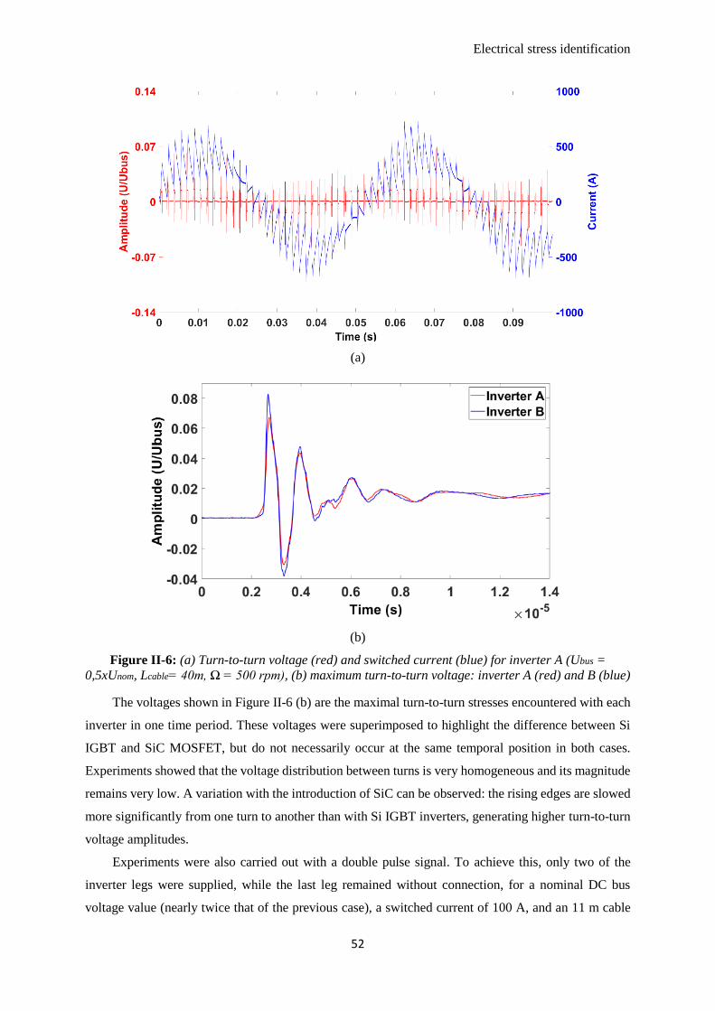
Electrical stress identification
52
(a)
(b)
Figure II-6: (a) Turn-to-turn voltage (red) and switched current (blue) for inverter A (Ubus =
0,5xUnom, Lcable= 40m, Ω = 500 rpm), (b) maximum turn-to-turn voltage: inverter A (red) and B (blue)
The voltages shown in Figure II-6 (b) are the maximal turn-to-turn stresses encountered with each
inverter in one time period. These voltages were superimposed to highlight the difference between Si
IGBT and SiC MOSFET, but do not necessarily occur at the same temporal position in both cases.
Experiments showed that the voltage distribution between turns is very homogeneous and its magnitude
remains very low. A variation with the introduction of SiC can be observed: the rising edges are slowed
more significantly from one turn to another than with Si IGBT inverters, generating higher turn-to-turn
voltage amplitudes.
Experiments were also carried out with a double pulse signal. To achieve this, only two of the
inverter legs were supplied, while the last leg remained without connection, for a nominal DC bus
voltage value (nearly twice that of the previous case), a switched current of 100 A, and an 11 m cable
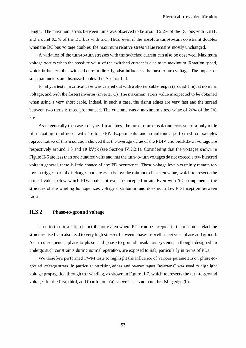
Electrical stress identification
53
length. The maximum stress between turns was observed to be around 5.2% of the DC bus with IGBT,
and around 8.3% of the DC bus with SiC. Thus, even if the absolute turn-to-turn constraint doubles
when the DC bus voltage doubles, the maximum relative stress value remains mostly unchanged.
A variation of the turn-to-turn stresses with the switched current can also be observed. Maximum
voltage occurs when the absolute value of the switched current is also at its maximum. Rotation speed,
which influences the switched current directly, also influences the turn-to-turn voltage. The impact of
such parameters are discussed in detail in Section II.4.
Finally, a test in a critical case was carried out with a shorter cable length (around 1 m), at nominal
voltage, and with the fastest inverter (inverter C). The maximum stress value is expected to be obtained
when using a very short cable. Indeed, in such a case, the rising edges are very fast and the spread
between two turns is most pronounced. The outcome was a maximum stress value of 20% of the DC
bus.
As is generally the case in Type II machines, the turn-to-turn insulation consists of a polyimide
film coating reinforced with Teflon-FEP. Experiments and simulations performed on samples
representative of this insulation showed that the average value of the PDIV and breakdown voltage are
respectively around 1.5 and 10 kVpk (see Section IV.2.2.1). Considering that the voltages shown in
Figure II-6 are less than one hundred volts and that the turn-to-turn voltages do not exceed a few hundred
volts in general, there is little chance of any PD occurrence. These voltage levels certainly remain too
low to trigger partial discharges and are even below the minimum Paschen value, which represents the
critical value below which PDs could not even be incepted in air. Even with SiC components, the
structure of the winding homogenizes voltage distribution and does not allow PD inception between
turns.
II.3.2 Phase-to-ground voltage
Turn-to-turn insulation is not the only area where PDs can be incepted in the machine. Machine
structure itself can also lead to very high stresses between phases as well as between phase and ground.
As a consequence, phase-to-phase and phase-to-ground insulation systems, although designed to
undergo such constraints during normal operation, are exposed to risk, particularly in terms of PDs.
We therefore performed PWM tests to highlight the influence of various parameters on phase-to-
ground voltage stress, in particular on rising edges and overvoltages. Inverter C was used to highlight
voltage propagation through the winding, as shown in Figure II-7, which represents the turn-to-ground
voltages for the first, third, and fourth turns (a), as well as a zoom on the rising edge (b).
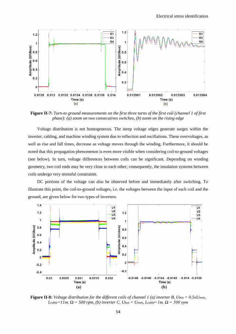
Electrical stress identification
54
Figure II-7: Turn-to ground measurements on the first three turns of the first coil (channel 1 of first
phase): (a) zoom on two consecutives switches, (b) zoom on the rising edge
Voltage distribution is not homogeneous. The steep voltage edges generate surges within the
inverter, cabling, and machine winding system due to reflection and oscillations. These overvoltages, as
well as rise and fall times, decrease as voltage moves through the winding. Furthermore, it should be
noted that this propagation phenomenon is even more visible when considering coil-to-ground voltages
(see below). In turn, voltage differences between coils can be significant. Depending on winding
geometry, two coil ends may be very close to each other; consequently, the insulation systems between
coils undergo very stressful constraints.
DC portions of the voltage can also be observed before and immediately after switching. To
illustrate this point, the coil-to-ground voltages, i.e. the voltages between the input of each coil and the
ground, are given below for two types of inverters.
Figure II-8: Voltage distribution for the different coils of channel 1 (a) inverter B, Ubus = 0.5xUnom,
Lcable=11m, Ω = 500 rpm, (b) inverter C, Ubus = Unom, Lcable=1m, Ω = 500 rpm
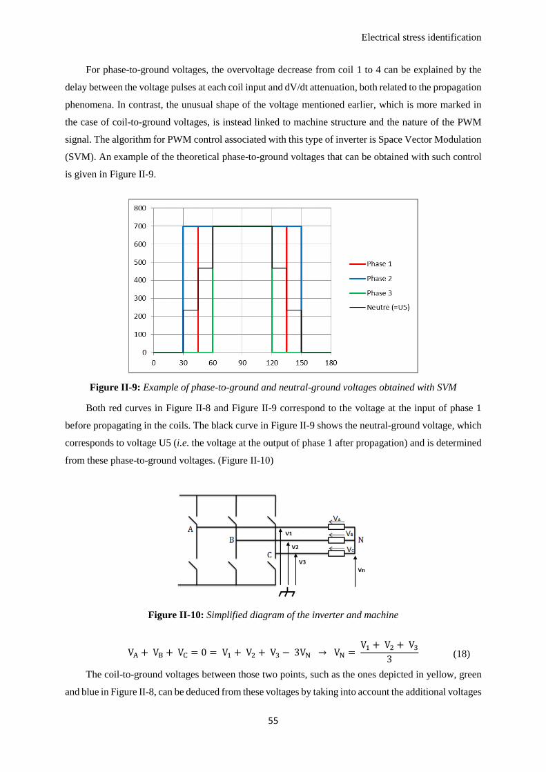
Electrical stress identification
55
For phase-to-ground voltages, the overvoltage decrease from coil 1 to 4 can be explained by the
delay between the voltage pulses at each coil input and dV/dt attenuation, both related to the propagation
phenomena. In contrast, the unusual shape of the voltage mentioned earlier, which is more marked in
the case of coil-to-ground voltages, is instead linked to machine structure and the nature of the PWM
signal. The algorithm for PWM control associated with this type of inverter is Space Vector Modulation
(SVM). An example of the theoretical phase-to-ground voltages that can be obtained with such control
is given in Figure II-9.
Figure II-9: Example of phase-to-ground and neutral-ground voltages obtained with SVM
Both red curves in Figure II-8 and Figure II-9 correspond to the voltage at the input of phase 1
before propagating in the coils. The black curve in Figure II-9 shows the neutral-ground voltage, which
corresponds to voltage U5 (i.e. the voltage at the output of phase 1 after propagation) and is determined
from these phase-to-ground voltages. (Figure II-10)
Figure II-10: Simplified diagram of the inverter and machine
VA + VB + VC = 0 = V1 + V2 + V3 − 3VN → VN = V1 + V2 + V3
3 (18)
The coil-to-ground voltages between those two points, such as the ones depicted in yellow, green
and blue in Figure II-8, can be deduced from these voltages by taking into account the additional voltages
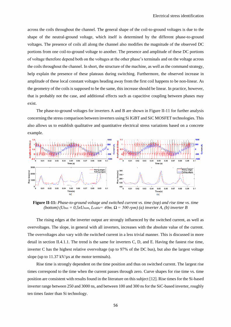
Electrical stress identification
56
across the coils throughout the channel. The general shape of the coil-to-ground voltages is due to the
shape of the neutral-ground voltage, which itself is determined by the different phase-to-ground
voltages. The presence of coils all along the channel also modifies the magnitude of the observed DC
portions from one coil-to-ground voltage to another. The presence and amplitude of these DC portions
of voltage therefore depend both on the voltages at the other phase’s terminals and on the voltage across
the coils throughout the channel. In short, the structure of the machine, as well as the command strategy,
help explain the presence of these plateaus during switching. Furthermore, the observed increase in
amplitude of these local constant voltages heading away from the first coil happens to be non-linear. As
the geometry of the coils is supposed to be the same, this increase should be linear. In practice, however,
that is probably not the case, and additional effects such as capacitive coupling between phases may
exist.
The phase-to-ground voltages for inverters A and B are shown in Figure II-11 for further analysis
concerning the stress comparison between inverters using Si IGBT and SiC MOSFET technologies. This
also allows us to establish qualitative and quantitative electrical stress variations based on a concrete
example.
Figure II-11: Phase-to-ground voltage and switched current vs. time (top) and rise time vs. time
(bottom) (Ubus = 0,5xUnom, Lcable= 40m, Ω = 500 rpm) (a) inverter A, (b) inverter B
The rising edges at the inverter output are strongly influenced by the switched current, as well as
overvoltages. The slope, in general with all inverters, increases with the absolute value of the current.
The overvoltages also vary with the switched current in a less trivial manner. This is discussed in more
detail in section II.4.1.1. The trend is the same for inverters C, D, and E. Having the fastest rise time,
inverter C has the highest relative overvoltage (up to 97% of the DC bus), but also the largest voltage
slope (up to 11.37 kV/µs at the motor terminals).
Rise time is strongly dependent on the time position and thus on switched current. The largest rise
times correspond to the time when the current passes through zero. Curve shapes for rise time vs. time
position are consistent with results found in the literature on this subject [12]. Rise times for the Si-based
inverter range between 250 and 3000 ns, and between 100 and 300 ns for the SiC-based inverter, roughly
ten times faster than Si technology.
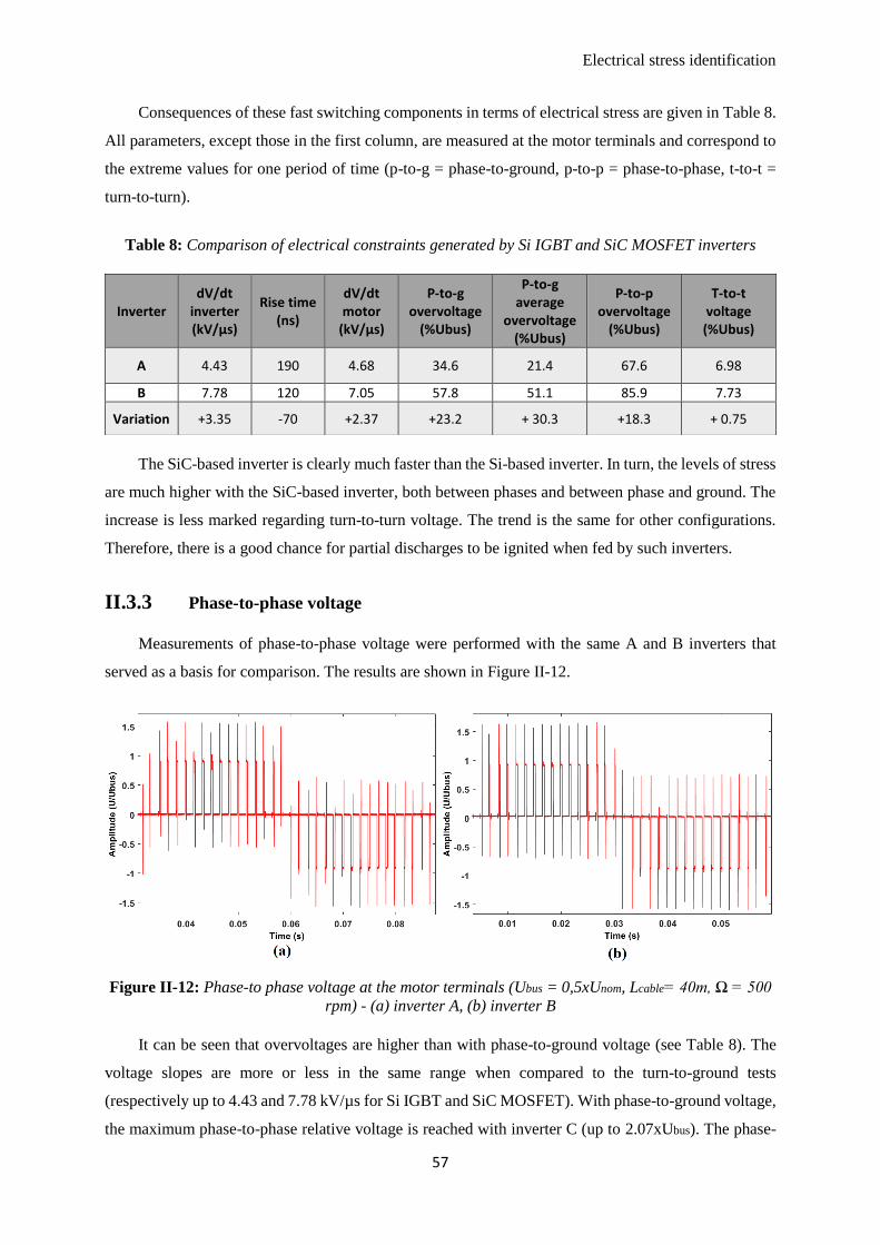
Electrical stress identification
57
Consequences of these fast switching components in terms of electrical stress are given in Table 8.
All parameters, except those in the first column, are measured at the motor terminals and correspond to
the extreme values for one period of time (p-to-g = phase-to-ground, p-to-p = phase-to-phase, t-to-t =
turn-to-turn).
Table 8: Comparison of electrical constraints generated by Si IGBT and SiC MOSFET inverters
The SiC-based inverter is clearly much faster than the Si-based inverter. In turn, the levels of stress
are much higher with the SiC-based inverter, both between phases and between phase and ground. The
increase is less marked regarding turn-to-turn voltage. The trend is the same for other configurations.
Therefore, there is a good chance for partial discharges to be ignited when fed by such inverters.
II.3.3 Phase-to-phase voltage
Measurements of phase-to-phase voltage were performed with the same A and B inverters that
served as a basis for comparison. The results are shown in Figure II-12.
Figure II-12: Phase-to phase voltage at the motor terminals (Ubus = 0,5xUnom, Lcable= 40m, Ω = 500
rpm) - (a) inverter A, (b) inverter B
It can be seen that overvoltages are higher than with phase-to-ground voltage (see Table 8). The
voltage slopes are more or less in the same range when compared to the turn-to-ground tests
(respectively up to 4.43 and 7.78 kV/µs for Si IGBT and SiC MOSFET). With phase-to-ground voltage,
the maximum phase-to-phase relative voltage is reached with inverter C (up to 2.07xUbus). The phase-
Inverter dV/dt
inverter (kV/µs)
Rise time (ns)
dV/dt motor
(kV/µs)
P-to-g overvoltage
(%Ubus)
P-to-g average
overvoltage (%Ubus)
P-to-p overvoltage
(%Ubus)
T-to-t voltage (%Ubus)
A 4.43 190 4.68 34.6 21.4 67.6 6.98
B 7.78 120 7.05 57.8 51.1 85.9 7.73
Variation +3.35 -70 +2.37 +23.2 + 30.3 +18.3 + 0.75
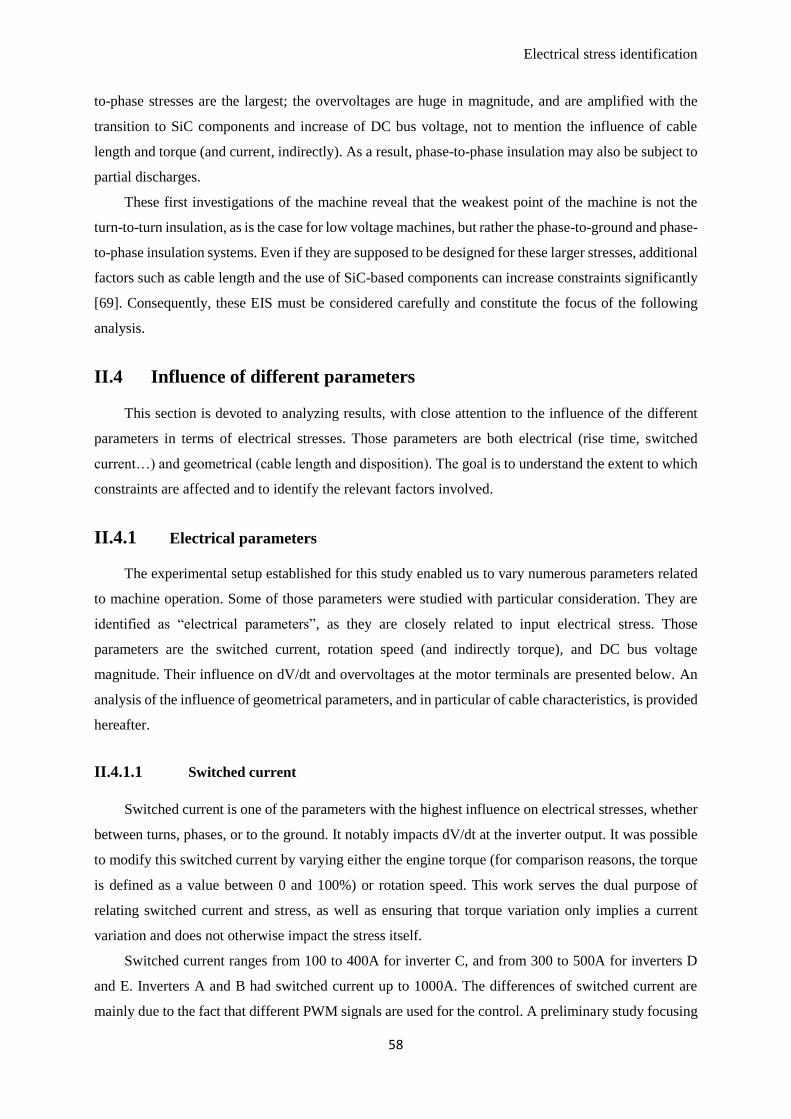
Electrical stress identification
58
to-phase stresses are the largest; the overvoltages are huge in magnitude, and are amplified with the
transition to SiC components and increase of DC bus voltage, not to mention the influence of cable
length and torque (and current, indirectly). As a result, phase-to-phase insulation may also be subject to
partial discharges.
These first investigations of the machine reveal that the weakest point of the machine is not the
turn-to-turn insulation, as is the case for low voltage machines, but rather the phase-to-ground and phase-
to-phase insulation systems. Even if they are supposed to be designed for these larger stresses, additional
factors such as cable length and the use of SiC-based components can increase constraints significantly
[69]. Consequently, these EIS must be considered carefully and constitute the focus of the following
analysis.
II.4 Influence of different parameters
This section is devoted to analyzing results, with close attention to the influence of the different
parameters in terms of electrical stresses. Those parameters are both electrical (rise time, switched
current…) and geometrical (cable length and disposition). The goal is to understand the extent to which
constraints are affected and to identify the relevant factors involved.
II.4.1 Electrical parameters
The experimental setup established for this study enabled us to vary numerous parameters related
to machine operation. Some of those parameters were studied with particular consideration. They are
identified as “electrical parameters”, as they are closely related to input electrical stress. Those
parameters are the switched current, rotation speed (and indirectly torque), and DC bus voltage
magnitude. Their influence on dV/dt and overvoltages at the motor terminals are presented below. An
analysis of the influence of geometrical parameters, and in particular of cable characteristics, is provided
hereafter.
II.4.1.1 Switched current
Switched current is one of the parameters with the highest influence on electrical stresses, whether
between turns, phases, or to the ground. It notably impacts dV/dt at the inverter output. It was possible
to modify this switched current by varying either the engine torque (for comparison reasons, the torque
is defined as a value between 0 and 100%) or rotation speed. This work serves the dual purpose of
relating switched current and stress, as well as ensuring that torque variation only implies a current
variation and does not otherwise impact the stress itself.
Switched current ranges from 100 to 400A for inverter C, and from 300 to 500A for inverters D
and E. Inverters A and B had switched current up to 1000A. The differences of switched current are
mainly due to the fact that different PWM signals are used for the control. A preliminary study focusing
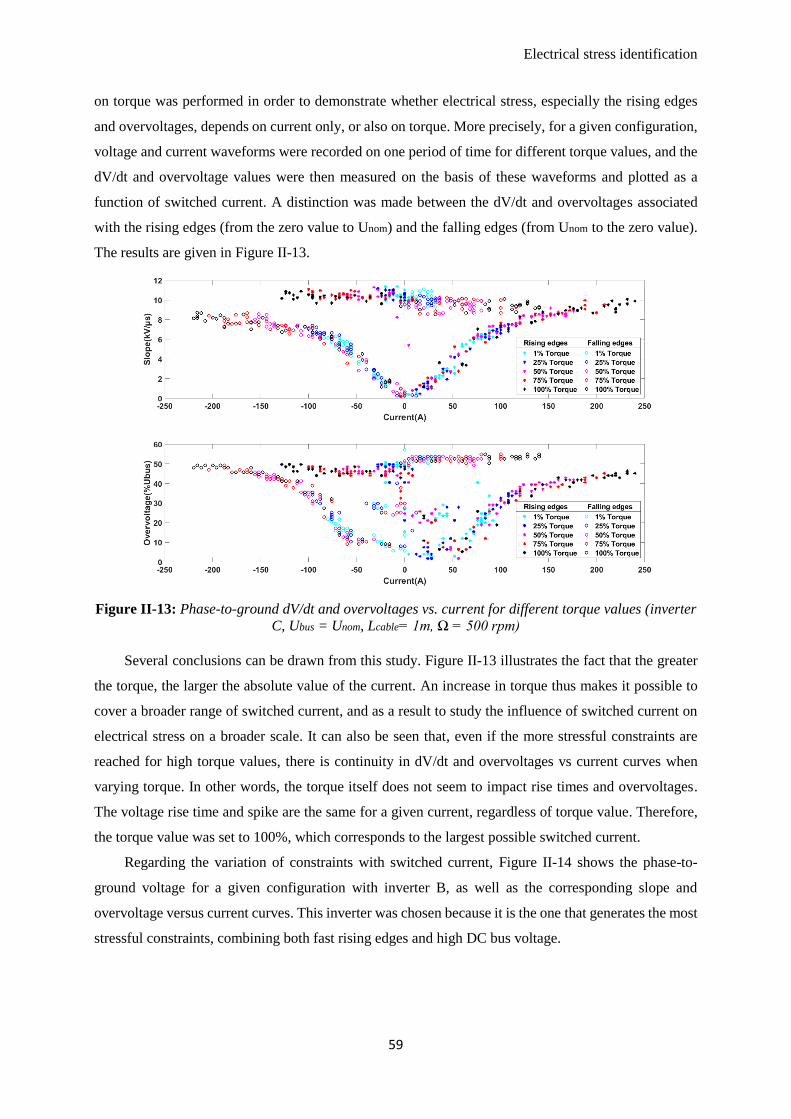
Electrical stress identification
59
on torque was performed in order to demonstrate whether electrical stress, especially the rising edges
and overvoltages, depends on current only, or also on torque. More precisely, for a given configuration,
voltage and current waveforms were recorded on one period of time for different torque values, and the
dV/dt and overvoltage values were then measured on the basis of these waveforms and plotted as a
function of switched current. A distinction was made between the dV/dt and overvoltages associated
with the rising edges (from the zero value to Unom) and the falling edges (from Unom to the zero value).
The results are given in Figure II-13.
Figure II-13: Phase-to-ground dV/dt and overvoltages vs. current for different torque values (inverter
C, Ubus = Unom, Lcable= 1m, Ω = 500 rpm)
Several conclusions can be drawn from this study. Figure II-13 illustrates the fact that the greater
the torque, the larger the absolute value of the current. An increase in torque thus makes it possible to
cover a broader range of switched current, and as a result to study the influence of switched current on
electrical stress on a broader scale. It can also be seen that, even if the more stressful constraints are
reached for high torque values, there is continuity in dV/dt and overvoltages vs current curves when
varying torque. In other words, the torque itself does not seem to impact rise times and overvoltages.
The voltage rise time and spike are the same for a given current, regardless of torque value. Therefore,
the torque value was set to 100%, which corresponds to the largest possible switched current.
Regarding the variation of constraints with switched current, Figure II-14 shows the phase-to-
ground voltage for a given configuration with inverter B, as well as the corresponding slope and
overvoltage versus current curves. This inverter was chosen because it is the one that generates the most
stressful constraints, combining both fast rising edges and high DC bus voltage.
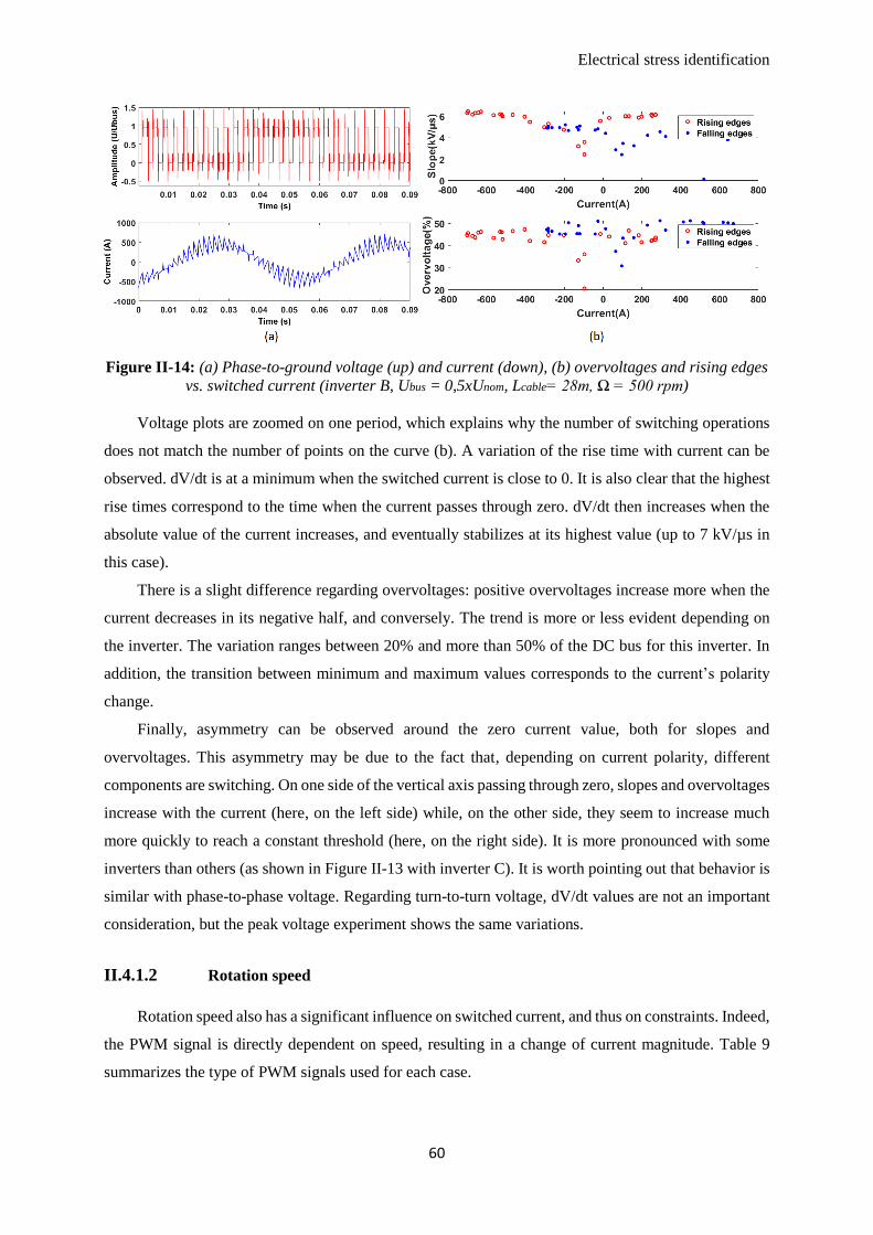
Electrical stress identification
60
Figure II-14: (a) Phase-to-ground voltage (up) and current (down), (b) overvoltages and rising edges
vs. switched current (inverter B, Ubus = 0,5xUnom, Lcable= 28m, Ω = 500 rpm)
Voltage plots are zoomed on one period, which explains why the number of switching operations
does not match the number of points on the curve (b). A variation of the rise time with current can be
observed. dV/dt is at a minimum when the switched current is close to 0. It is also clear that the highest
rise times correspond to the time when the current passes through zero. dV/dt then increases when the
absolute value of the current increases, and eventually stabilizes at its highest value (up to 7 kV/µs in
this case).
There is a slight difference regarding overvoltages: positive overvoltages increase more when the
current decreases in its negative half, and conversely. The trend is more or less evident depending on
the inverter. The variation ranges between 20% and more than 50% of the DC bus for this inverter. In
addition, the transition between minimum and maximum values corresponds to the current’s polarity
change.
Finally, asymmetry can be observed around the zero current value, both for slopes and
overvoltages. This asymmetry may be due to the fact that, depending on current polarity, different
components are switching. On one side of the vertical axis passing through zero, slopes and overvoltages
increase with the current (here, on the left side) while, on the other side, they seem to increase much
more quickly to reach a constant threshold (here, on the right side). It is more pronounced with some
inverters than others (as shown in Figure II-13 with inverter C). It is worth pointing out that behavior is
similar with phase-to-phase voltage. Regarding turn-to-turn voltage, dV/dt values are not an important
consideration, but the peak voltage experiment shows the same variations.
II.4.1.2 Rotation speed
Rotation speed also has a significant influence on switched current, and thus on constraints. Indeed,
the PWM signal is directly dependent on speed, resulting in a change of current magnitude. Table 9
summarizes the type of PWM signals used for each case.
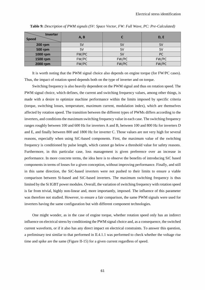
Electrical stress identification
61
Table 9: Description of PWM signals (SV: Space Vector, FW: Full Wave, PC: Pre-Calculated)
Inverter Speed
A, B C D, E
200 rpm SV SV SV
500 rpm SV SV SV
1000 rpm FW/PC SV PC
1500 rpm FW/PC FW/PC FW/PC
2000 rpm FW/PC FW/PC FW/PC
It is worth noting that the PWM signal choice also depends on engine torque (for FW/PC cases).
Thus, the impact of rotation speed depends both on the type of inverter and on torque.
Switching frequency is also heavily dependent on the PWM signal and thus on rotation speed. The
PWM signal choice, which defines, the current and switching frequency values, among other things, is
made with a desire to optimize machine performance within the limits imposed by specific criteria
(torque, switching losses, temperature, maximum current, modulation index), which are themselves
affected by rotation speed. The transition between the different types of PWMs differs according to the
inverters, and conditions the maximum switching frequency value in each case. The switching frequency
ranges roughly between 100 and 600 Hz for inverters A and B, between 100 and 800 Hz for inverters D
and E, and finally between 800 and 1800 Hz for inverter C. Those values are not very high for several
reasons, especially when using SiC-based components. First, the maximum value of the switching
frequency is conditioned by pulse length, which cannot go below a threshold value for safety reasons.
Furthermore, in this particular case, loss management is given preference over an increase in
performance. In more concrete terms, the idea here is to observe the benefits of introducing SiC based
components in terms of losses for a given conception, without improving performance. Finally, and still
in this same direction, the SiC-based inverters were not pushed to their limits to ensure a viable
comparison between Si-based and SiC-based inverters. The maximum switching frequency is thus
limited by the Si IGBT power modules. Overall, the variation of switching frequency with rotation speed
is far from trivial, highly non-linear and, more importantly, imposed. The influence of this parameter
was therefore not studied. However, to ensure a fair comparison, the same PWM signals were used for
inverters having the same configuration but with different component technologies.
One might wonder, as in the case of engine torque, whether rotation speed only has an indirect
influence on electrical stress by conditioning the PWM signal choice and, as a consequence, the switched
current waveform, or if it also has any direct impact on electrical constraints. To answer this question,
a preliminary test similar to that performed in II.4.1.1 was performed to check whether the voltage rise
time and spike are the same (Figure II-15) for a given current regardless of speed.
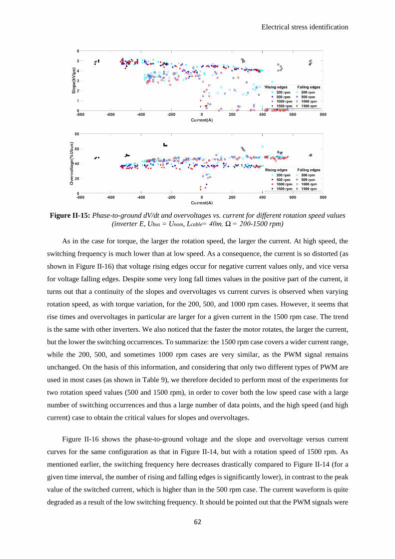
Electrical stress identification
62
Figure II-15: Phase-to-ground dV/dt and overvoltages vs. current for different rotation speed values
(inverter E, Ubus = Unom, Lcable= 40m, Ω = 200-1500 rpm)
As in the case for torque, the larger the rotation speed, the larger the current. At high speed, the
switching frequency is much lower than at low speed. As a consequence, the current is so distorted (as
shown in Figure II-16) that voltage rising edges occur for negative current values only, and vice versa
for voltage falling edges. Despite some very long fall times values in the positive part of the current, it
turns out that a continuity of the slopes and overvoltages vs current curves is observed when varying
rotation speed, as with torque variation, for the 200, 500, and 1000 rpm cases. However, it seems that
rise times and overvoltages in particular are larger for a given current in the 1500 rpm case. The trend
is the same with other inverters. We also noticed that the faster the motor rotates, the larger the current,
but the lower the switching occurrences. To summarize: the 1500 rpm case covers a wider current range,
while the 200, 500, and sometimes 1000 rpm cases are very similar, as the PWM signal remains
unchanged. On the basis of this information, and considering that only two different types of PWM are
used in most cases (as shown in Table 9), we therefore decided to perform most of the experiments for
two rotation speed values (500 and 1500 rpm), in order to cover both the low speed case with a large
number of switching occurrences and thus a large number of data points, and the high speed (and high
current) case to obtain the critical values for slopes and overvoltages.
Figure II-16 shows the phase-to-ground voltage and the slope and overvoltage versus current
curves for the same configuration as that in Figure II-14, but with a rotation speed of 1500 rpm. As
mentioned earlier, the switching frequency here decreases drastically compared to Figure II-14 (for a
given time interval, the number of rising and falling edges is significantly lower), in contrast to the peak
value of the switched current, which is higher than in the 500 rpm case. The current waveform is quite
degraded as a result of the low switching frequency. It should be pointed out that the PWM signals were
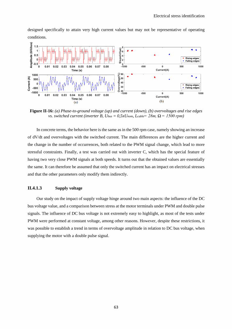
Electrical stress identification
63
designed specifically to attain very high current values but may not be representative of operating
conditions.
Figure II-16: (a) Phase-to-ground voltage (up) and current (down), (b) overvoltages and rise edges
vs. switched current (inverter B, Ubus = 0,5xUnom, Lcable= 28m, Ω = 1500 rpm)
In concrete terms, the behavior here is the same as in the 500 rpm case, namely showing an increase
of dV/dt and overvoltages with the switched current. The main differences are the higher current and
the change in the number of occurrences, both related to the PWM signal change, which lead to more
stressful constraints. Finally, a test was carried out with inverter C, which has the special feature of
having two very close PWM signals at both speeds. It turns out that the obtained values are essentially
the same. It can therefore be assumed that only the switched current has an impact on electrical stresses
and that the other parameters only modify them indirectly.
II.4.1.3 Supply voltage
Our study on the impact of supply voltage hinge around two main aspects: the influence of the DC
bus voltage value, and a comparison between stress at the motor terminals under PWM and double pulse
signals. The influence of DC bus voltage is not extremely easy to highlight, as most of the tests under
PWM were performed at constant voltage, among other reasons. However, despite these restrictions, it
was possible to establish a trend in terms of overvoltage amplitude in relation to DC bus voltage, when
supplying the motor with a double pulse signal.
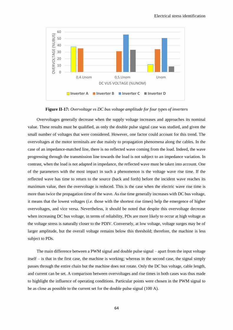
Electrical stress identification
64
Figure II-17: Overvoltage vs DC bus voltage amplitude for four types of inverters
Overvoltages generally decrease when the supply voltage increases and approaches its nominal
value. These results must be qualified, as only the double pulse signal case was studied, and given the
small number of voltages that were considered. However, one factor could account for this trend. The
overvoltages at the motor terminals are due mainly to propagation phenomena along the cables. In the
case of an impedance-matched line, there is no reflected wave coming from the load. Indeed, the wave
progressing through the transmission line towards the load is not subject to an impedance variation. In
contrast, when the load is not adapted in impedance, the reflected wave must be taken into account. One
of the parameters with the most impact in such a phenomenon is the voltage wave rise time. If the
reflected wave has time to return to the source (back and forth) before the incident wave reaches its
maximum value, then the overvoltage is reduced. This is the case when the electric wave rise time is
more than twice the propagation time of the wave. As rise time generally increases with DC bus voltage,
it means that the lowest voltages (i.e. those with the shortest rise times) help the emergence of higher
overvoltages, and vice versa. Nevertheless, it should be noted that despite this overvoltage decrease
when increasing DC bus voltage, in terms of reliability, PDs are more likely to occur at high voltage as
the voltage stress is naturally closer to the PDIV. Conversely, at low voltage, voltage surges may be of
larger amplitude, but the overall voltage remains below this threshold; therefore, the machine is less
subject to PDs.
The main difference between a PWM signal and double pulse signal – apart from the input voltage
itself – is that in the first case, the machine is working; whereas in the second case, the signal simply
passes through the entire chain but the machine does not rotate. Only the DC bus voltage, cable length,
and current can be set. A comparison between overvoltages and rise times in both cases was thus made
to highlight the influence of operating conditions. Particular points were chosen in the PWM signal to
be as close as possible to the current set for the double pulse signal (100 A).
0
10
20
30
40
50
60
0,4.Unom 0,5.Unom Unom
OV
ERV
OLT
AG
E (%
UB
US)
DC VUS VOLTAGE (%UNOM)
Inverter A Inverter B Inverter C Inverter D
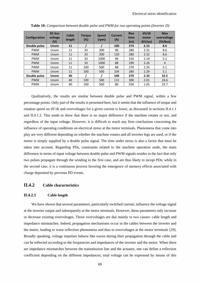
Electrical stress identification
65
Table 10: Comparison between double pulse and PWM for two operating points (Inverter D)
Configuration DC bus voltage
(V)
Cable length
Torque (%)
Speed (rpm)
Current (A)
Rise time (ns)
dV/dt motor
(kV/µs)
Max overvoltage
(%Ubus)
Double pulse Unom 11 / / 100 274 2.15 8.6
PWM Unom 11 33 200 96 280 2.31 8.6
PWM Unom 11 33 200 120 280 2.32 8.6
PWM Unom 11 33 1000 96 310 2.19 5.1
PWM Unom 11 33 1000 88 290 2.26 4
PWM Unom 11 100 500 88 270 2.35 5.1
PWM Unom 11 100 500 104 280 2.29 5.1
Double pulse Unom 40 / / 100 270 2.32 32.5
PWM Unom 40 100 500 112 300 2.01 24.6
PWM Unom 40 100 500 80 550 1.05 25.7
Qualitatively, the results are similar between double pulse and PWM signal, within a few
percentage points. Only part of the results is presented here, but it seems that the influence of torque and
rotation speed on dV/dt and overvoltages for a given current is lower, as discussed in sections II.4.1.1
and II.4.1.2. This tends to show that there is no major difference if the machine rotates or not, and
regardless of the input voltage. However, it is difficult to reach any firm conclusions concerning the
influence of operating conditions on electrical stress at the motor terminals. Phenomena that come into
play are very different depending on whether the machine rotates and all inverter legs are used, or if the
motor is simply supplied by a double pulse signal. The time under stress is also a factor that must be
taken into account. Regarding PDs, constraints related to the machine operation aside, the main
difference in terms of input voltage between double pulse and PWM signals resides in the fact that only
two pulses propagate through the winding in the first case, and are thus likely to incept PDs; while in
the second case, it is a continuous process favoring the emergence of memory effects associated with
charge deposited by previous PD events.
II.4.2 Cable characteristics
II.4.2.1 Cable length
We have shown that several parameters, particularly switched current, influence the voltage signal
at the inverter output and subsequently at the motor terminals. However, these parameters only increase
or decrease existing overvoltages. Those overvoltages are due mainly to two causes: cable length and
impedance mismatches. Indeed, propagation mechanisms occur in the cables between the inverter and
the motor, leading to wave reflection phenomena and thus to overvoltages at the motor terminals [29].
Broadly speaking, voltage impulses behave like waves during their propagation through the cable and
can be reflected according to the frequencies and impedances of the inverter and the motor. When there
are impedance mismatches between the transmission line and the actuator, one can define a reflection
coefficient depending on the different impedances; total voltage can be expressed by means of this
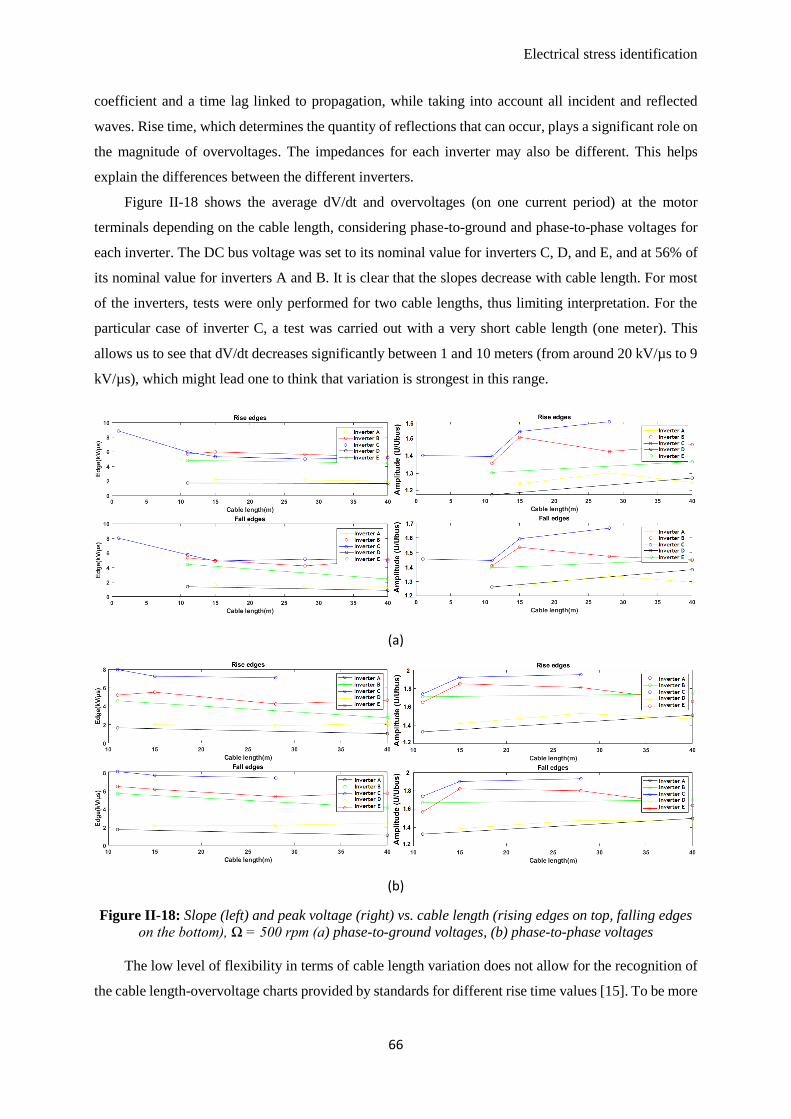
Electrical stress identification
66
coefficient and a time lag linked to propagation, while taking into account all incident and reflected
waves. Rise time, which determines the quantity of reflections that can occur, plays a significant role on
the magnitude of overvoltages. The impedances for each inverter may also be different. This helps
explain the differences between the different inverters.
Figure II-18 shows the average dV/dt and overvoltages (on one current period) at the motor
terminals depending on the cable length, considering phase-to-ground and phase-to-phase voltages for
each inverter. The DC bus voltage was set to its nominal value for inverters C, D, and E, and at 56% of
its nominal value for inverters A and B. It is clear that the slopes decrease with cable length. For most
of the inverters, tests were only performed for two cable lengths, thus limiting interpretation. For the
particular case of inverter C, a test was carried out with a very short cable length (one meter). This
allows us to see that dV/dt decreases significantly between 1 and 10 meters (from around 20 kV/µs to 9
kV/µs), which might lead one to think that variation is strongest in this range.
(a)
(b)
Figure II-18: Slope (left) and peak voltage (right) vs. cable length (rising edges on top, falling edges
on the bottom), Ω = 500 rpm (a) phase-to-ground voltages, (b) phase-to-phase voltages
The low level of flexibility in terms of cable length variation does not allow for the recognition of
the cable length-overvoltage charts provided by standards for different rise time values [15]. To be more
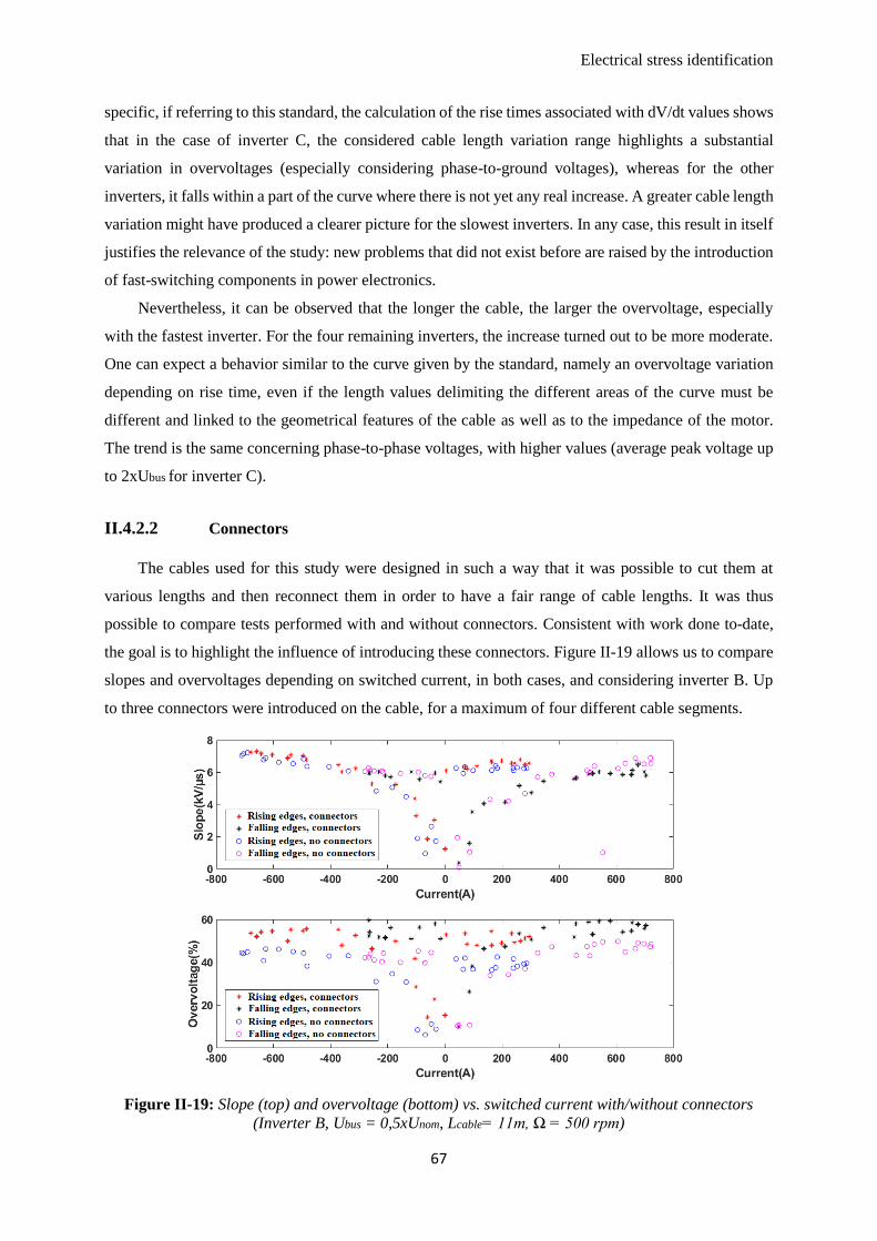
Electrical stress identification
67
specific, if referring to this standard, the calculation of the rise times associated with dV/dt values shows
that in the case of inverter C, the considered cable length variation range highlights a substantial
variation in overvoltages (especially considering phase-to-ground voltages), whereas for the other
inverters, it falls within a part of the curve where there is not yet any real increase. A greater cable length
variation might have produced a clearer picture for the slowest inverters. In any case, this result in itself
justifies the relevance of the study: new problems that did not exist before are raised by the introduction
of fast-switching components in power electronics.
Nevertheless, it can be observed that the longer the cable, the larger the overvoltage, especially
with the fastest inverter. For the four remaining inverters, the increase turned out to be more moderate.
One can expect a behavior similar to the curve given by the standard, namely an overvoltage variation
depending on rise time, even if the length values delimiting the different areas of the curve must be
different and linked to the geometrical features of the cable as well as to the impedance of the motor.
The trend is the same concerning phase-to-phase voltages, with higher values (average peak voltage up
to 2xUbus for inverter C).
II.4.2.2 Connectors
The cables used for this study were designed in such a way that it was possible to cut them at
various lengths and then reconnect them in order to have a fair range of cable lengths. It was thus
possible to compare tests performed with and without connectors. Consistent with work done to-date,
the goal is to highlight the influence of introducing these connectors. Figure II-19 allows us to compare
slopes and overvoltages depending on switched current, in both cases, and considering inverter B. Up
to three connectors were introduced on the cable, for a maximum of four different cable segments.
Figure II-19: Slope (top) and overvoltage (bottom) vs. switched current with/without connectors
(Inverter B, Ubus = 0,5xUnom, Lcable= 11m, Ω = 500 rpm)
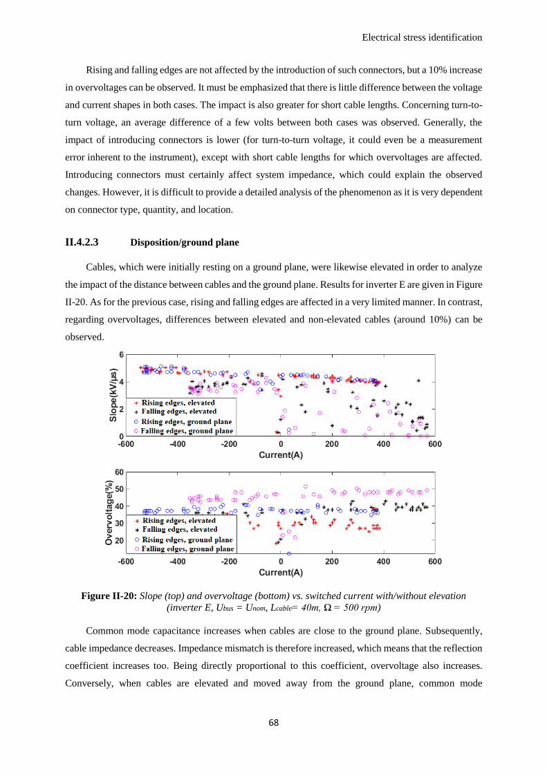
Electrical stress identification
68
Rising and falling edges are not affected by the introduction of such connectors, but a 10% increase
in overvoltages can be observed. It must be emphasized that there is little difference between the voltage
and current shapes in both cases. The impact is also greater for short cable lengths. Concerning turn-to-
turn voltage, an average difference of a few volts between both cases was observed. Generally, the
impact of introducing connectors is lower (for turn-to-turn voltage, it could even be a measurement
error inherent to the instrument), except with short cable lengths for which overvoltages are affected.
Introducing connectors must certainly affect system impedance, which could explain the observed
changes. However, it is difficult to provide a detailed analysis of the phenomenon as it is very dependent
on connector type, quantity, and location.
II.4.2.3 Disposition/ground plane
Cables, which were initially resting on a ground plane, were likewise elevated in order to analyze
the impact of the distance between cables and the ground plane. Results for inverter E are given in Figure
II-20. As for the previous case, rising and falling edges are affected in a very limited manner. In contrast,
regarding overvoltages, differences between elevated and non-elevated cables (around 10%) can be
observed.
Figure II-20: Slope (top) and overvoltage (bottom) vs. switched current with/without elevation
(inverter E, Ubus = Unom, Lcable= 40m, Ω = 500 rpm)
Common mode capacitance increases when cables are close to the ground plane. Subsequently,
cable impedance decreases. Impedance mismatch is therefore increased, which means that the reflection
coefficient increases too. Being directly proportional to this coefficient, overvoltage also increases.
Conversely, when cables are elevated and moved away from the ground plane, common mode
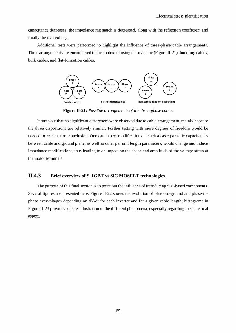
Electrical stress identification
69
capacitance decreases, the impedance mismatch is decreased, along with the reflection coefficient and
finally the overvoltage.
Additional tests were performed to highlight the influence of three-phase cable arrangements.
Three arrangements are encountered in the context of using our machine (Figure II-21): bundling cables,
bulk cables, and flat-formation cables.
Figure II-21: Possible arrangements of the three-phase cables
It turns out that no significant differences were observed due to cable arrangement, mainly because
the three dispositions are relatively similar. Further testing with more degrees of freedom would be
needed to reach a firm conclusion. One can expect modifications in such a case: parasitic capacitances
between cable and ground plane, as well as other per unit length parameters, would change and induce
impedance modifications, thus leading to an impact on the shape and amplitude of the voltage stress at
the motor terminals
II.4.3 Brief overview of Si IGBT vs SiC MOSFET technologies
The purpose of this final section is to point out the influence of introducing SiC-based components.
Several figures are presented here. Figure II-22 shows the evolution of phase-to-ground and phase-to-
phase overvoltages depending on dV/dt for each inverter and for a given cable length; histograms in
Figure II-23 provide a clearer illustration of the different phenomena, especially regarding the statistical
aspect.
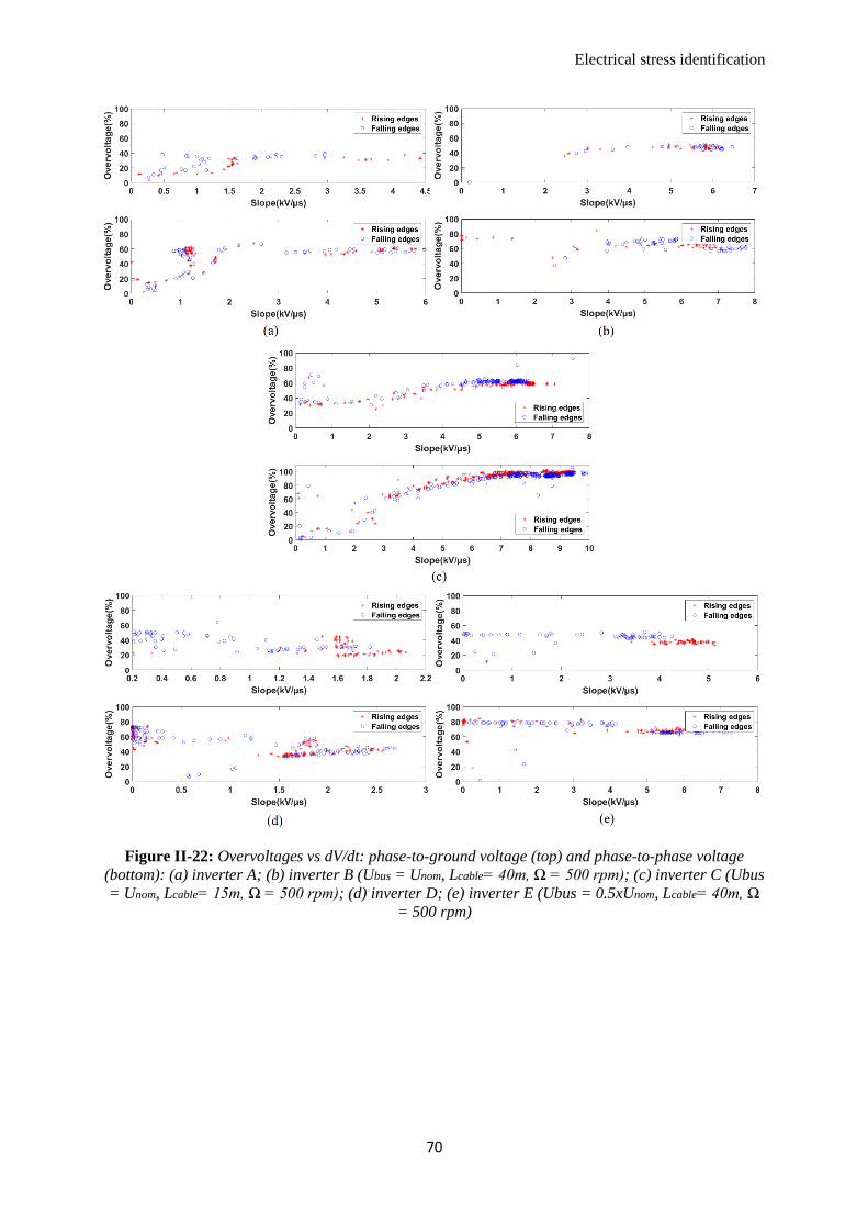
Electrical stress identification
70
Figure II-22: Overvoltages vs dV/dt: phase-to-ground voltage (top) and phase-to-phase voltage
(bottom): (a) inverter A; (b) inverter B (Ubus = Unom, Lcable= 40m, Ω = 500 rpm); (c) inverter C (Ubus
= Unom, Lcable= 15m, Ω = 500 rpm); (d) inverter D; (e) inverter E (Ubus = 0.5xUnom, Lcable= 40m, Ω
= 500 rpm)
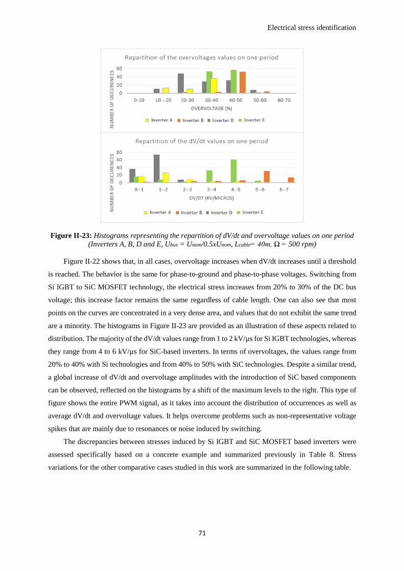
Electrical stress identification
71
Figure II-23: Histograms representing the repartition of dV/dt and overvoltage values on one period
(Inverters A, B, D and E, Ubus = Unom/0.5xUnom, Lcable= 40m, Ω = 500 rpm)
Figure II-22 shows that, in all cases, overvoltage increases when dV/dt increases until a threshold
is reached. The behavior is the same for phase-to-ground and phase-to-phase voltages. Switching from
Si IGBT to SiC MOSFET technology, the electrical stress increases from 20% to 30% of the DC bus
voltage; this increase factor remains the same regardless of cable length. One can also see that most
points on the curves are concentrated in a very dense area, and values that do not exhibit the same trend
are a minority. The histograms in Figure II-23 are provided as an illustration of these aspects related to
distribution. The majority of the dV/dt values range from 1 to 2 kV/µs for Si IGBT technologies, whereas
they range from 4 to 6 kV/µs for SiC-based inverters. In terms of overvoltages, the values range from
20% to 40% with Si technologies and from 40% to 50% with SiC technologies. Despite a similar trend,
a global increase of dV/dt and overvoltage amplitudes with the introduction of SiC based components
can be observed, reflected on the histograms by a shift of the maximum levels to the right. This type of
figure shows the entire PWM signal, as it takes into account the distribution of occurrences as well as
average dV/dt and overvoltage values. It helps overcome problems such as non-representative voltage
spikes that are mainly due to resonances or noise induced by switching.
The discrepancies between stresses induced by Si IGBT and SiC MOSFET based inverters were
assessed specifically based on a concrete example and summarized previously in Table 8. Stress
variations for the other comparative cases studied in this work are summarized in the following table.
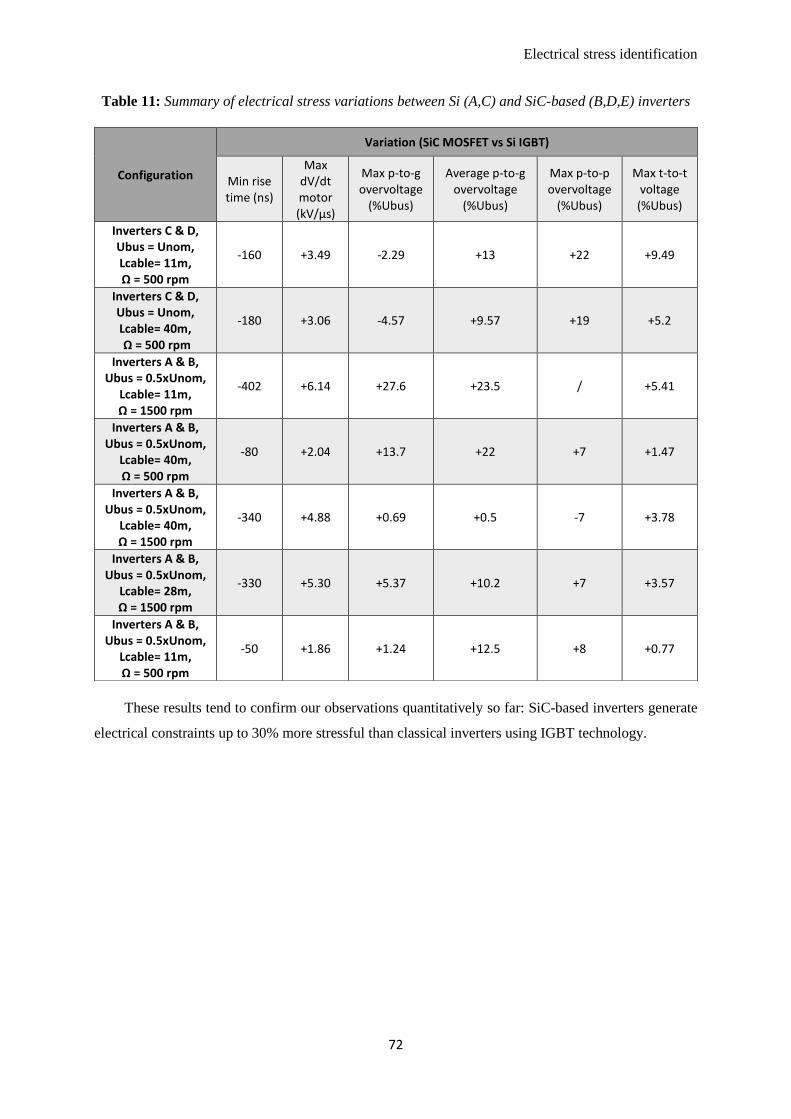
Electrical stress identification
72
Table 11: Summary of electrical stress variations between Si (A,C) and SiC-based (B,D,E) inverters
These results tend to confirm our observations quantitatively so far: SiC-based inverters generate
electrical constraints up to 30% more stressful than classical inverters using IGBT technology.
Configuration
Variation (SiC MOSFET vs Si IGBT)
Min rise time (ns)
Max dV/dt motor (kV/µs)
Max p-to-g overvoltage
(%Ubus)
Average p-to-g overvoltage
(%Ubus)
Max p-to-p overvoltage
(%Ubus)
Max t-to-t voltage (%Ubus)
Inverters C & D, Ubus = Unom, Lcable= 11m, Ω = 500 rpm
-160 +3.49 -2.29 +13 +22 +9.49
Inverters C & D, Ubus = Unom, Lcable= 40m, Ω = 500 rpm
-180 +3.06 -4.57 +9.57 +19 +5.2
Inverters A & B, Ubus = 0.5xUnom,
Lcable= 11m, Ω = 1500 rpm
-402 +6.14 +27.6 +23.5 / +5.41
Inverters A & B, Ubus = 0.5xUnom,
Lcable= 40m, Ω = 500 rpm
-80 +2.04 +13.7 +22 +7 +1.47
Inverters A & B, Ubus = 0.5xUnom,
Lcable= 40m, Ω = 1500 rpm
-340 +4.88 +0.69 +0.5 -7 +3.78
Inverters A & B, Ubus = 0.5xUnom,
Lcable= 28m, Ω = 1500 rpm
-330 +5.30 +5.37 +10.2 +7 +3.57
Inverters A & B, Ubus = 0.5xUnom,
Lcable= 11m, Ω = 500 rpm
-50 +1.86 +1.24 +12.5 +8 +0.77
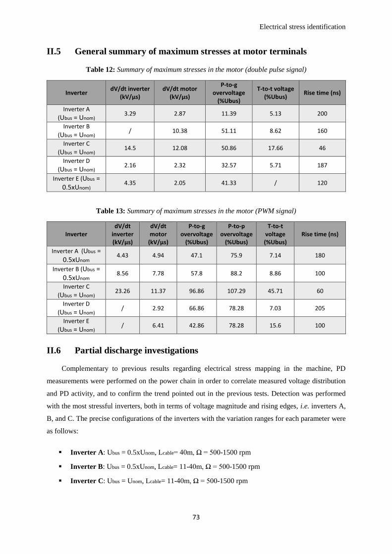
Electrical stress identification
73
II.5 General summary of maximum stresses at motor terminals
Table 12: Summary of maximum stresses in the motor (double pulse signal)
Inverter dV/dt inverter
(kV/µs) dV/dt motor
(kV/µs)
P-to-g overvoltage
(%Ubus)
T-to-t voltage (%Ubus)
Rise time (ns)
Inverter A
(Ubus = Unom) 3.29 2.87 11.39 5.13 200
Inverter B
(Ubus = Unom) / 10.38 51.11 8.62 160
Inverter C
(Ubus = Unom) 14.5 12.08 50.86 17.66 46
Inverter D
(Ubus = Unom) 2.16 2.32 32.57 5.71 187
Inverter E (Ubus = 0.5xUnom)
4.35 2.05 41.33 / 120
Table 13: Summary of maximum stresses in the motor (PWM signal)
Inverter dV/dt
inverter (kV/µs)
dV/dt motor
(kV/µs)
P-to-g overvoltage
(%Ubus)
P-to-p overvoltage
(%Ubus)
T-to-t voltage (%Ubus)
Rise time (ns)
Inverter A (Ubus = 0.5xUnom
4.43 4.94 47.1 75.9 7.14 180
Inverter B (Ubus = 0.5xUnom
8.56 7.78 57.8 88.2 8.86 100
Inverter C
(Ubus = Unom) 23.26 11.37 96.86 107.29 45.71 60
Inverter D
(Ubus = Unom) / 2.92 66.86 78.28 7.03 205
Inverter E
(Ubus = Unom) / 6.41 42.86 78.28 15.6 100
II.6 Partial discharge investigations
Complementary to previous results regarding electrical stress mapping in the machine, PD
measurements were performed on the power chain in order to correlate measured voltage distribution
and PD activity, and to confirm the trend pointed out in the previous tests. Detection was performed
with the most stressful inverters, both in terms of voltage magnitude and rising edges, i.e. inverters A,
B, and C. The precise configurations of the inverters with the variation ranges for each parameter were
as follows:
Inverter A: Ubus = 0.5xUnom, Lcable= 40m, Ω = 500-1500 rpm
Inverter B: Ubus = 0.5xUnom, Lcable= 11-40m, Ω = 500-1500 rpm
Inverter C: Ubus = Unom, Lcable= 11-40m, Ω = 500-1500 rpm
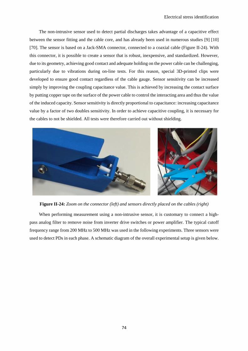
Electrical stress identification
74
The non-intrusive sensor used to detect partial discharges takes advantage of a capacitive effect
between the sensor fitting and the cable core, and has already been used in numerous studies [9] [10]
[70]. The sensor is based on a Jack-SMA connector, connected to a coaxial cable (Figure II-24). With
this connector, it is possible to create a sensor that is robust, inexpensive, and standardized. However,
due to its geometry, achieving good contact and adequate holding on the power cable can be challenging,
particularly due to vibrations during on-line tests. For this reason, special 3D-printed clips were
developed to ensure good contact regardless of the cable gauge. Sensor sensitivity can be increased
simply by improving the coupling capacitance value. This is achieved by increasing the contact surface
by putting copper tape on the surface of the power cable to control the interacting area and thus the value
of the induced capacity. Sensor sensitivity is directly proportional to capacitance: increasing capacitance
value by a factor of two doubles sensitivity. In order to achieve capacitive coupling, it is necessary for
the cables to not be shielded. All tests were therefore carried out without shielding.
Figure II-24: Zoom on the connector (left) and sensors directly placed on the cables (right)
When performing measurement using a non-intrusive sensor, it is customary to connect a high-
pass analog filter to remove noise from inverter drive switches or power amplifier. The typical cutoff
frequency range from 200 MHz to 500 MHz was used in the following experiments. Three sensors were
used to detect PDs in each phase. A schematic diagram of the overall experimental setup is given below.
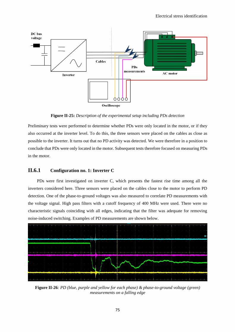
Electrical stress identification
75
Figure II-25: Description of the experimental setup including PDs detection
Preliminary tests were performed to determine whether PDs were only located in the motor, or if they
also occurred at the inverter level. To do this, the three sensors were placed on the cables as close as
possible to the inverter. It turns out that no PD activity was detected. We were therefore in a position to
conclude that PDs were only located in the motor. Subsequent tests therefore focused on measuring PDs
in the motor.
II.6.1 Configuration no. 1: Inverter C
PDs were first investigated on inverter C, which presents the fastest rise time among all the
inverters considered here. Three sensors were placed on the cables close to the motor to perform PD
detection. One of the phase-to-ground voltages was also measured to correlate PD measurements with
the voltage signal. High pass filters with a cutoff frequency of 400 MHz were used. There were no
characteristic signals coinciding with all edges, indicating that the filter was adequate for removing
noise-induced switching. Examples of PD measurements are shown below.
Figure II-26: PD (blue, purple and yellow for each phase) & phase-to-ground voltage (green)
measurements on a falling edge
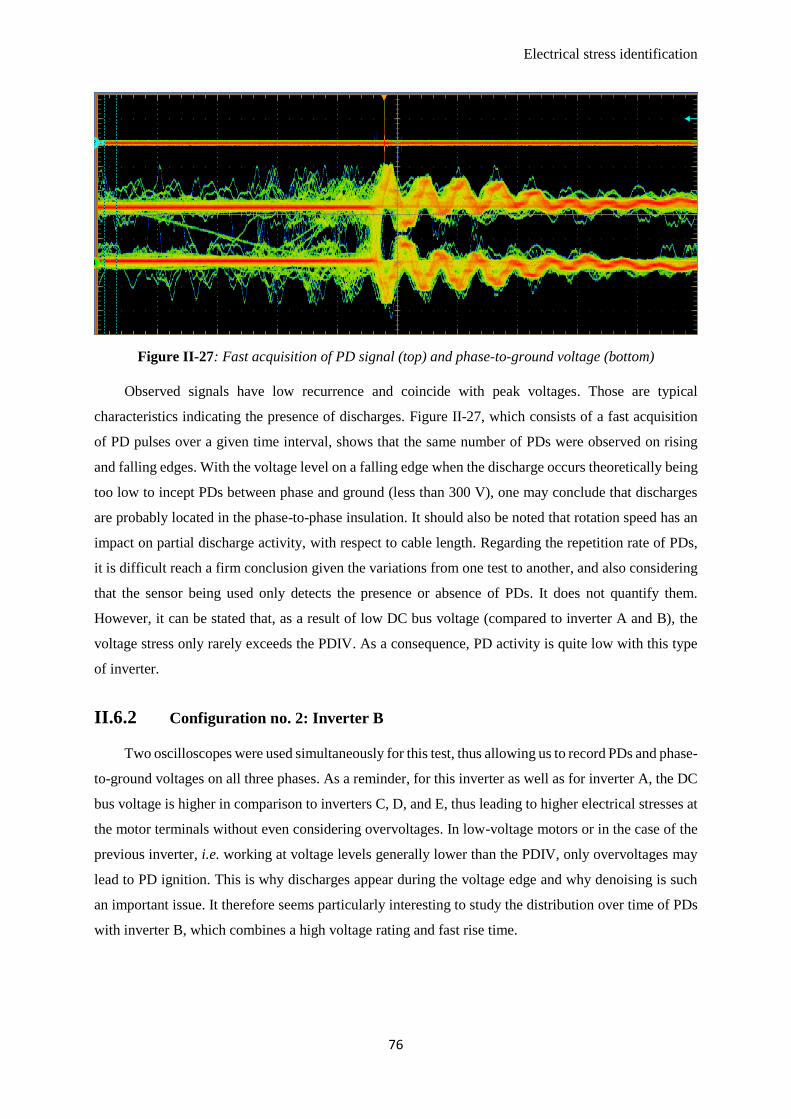
Electrical stress identification
76
Figure II-27: Fast acquisition of PD signal (top) and phase-to-ground voltage (bottom)
Observed signals have low recurrence and coincide with peak voltages. Those are typical
characteristics indicating the presence of discharges. Figure II-27, which consists of a fast acquisition
of PD pulses over a given time interval, shows that the same number of PDs were observed on rising
and falling edges. With the voltage level on a falling edge when the discharge occurs theoretically being
too low to incept PDs between phase and ground (less than 300 V), one may conclude that discharges
are probably located in the phase-to-phase insulation. It should also be noted that rotation speed has an
impact on partial discharge activity, with respect to cable length. Regarding the repetition rate of PDs,
it is difficult reach a firm conclusion given the variations from one test to another, and also considering
that the sensor being used only detects the presence or absence of PDs. It does not quantify them.
However, it can be stated that, as a result of low DC bus voltage (compared to inverter A and B), the
voltage stress only rarely exceeds the PDIV. As a consequence, PD activity is quite low with this type
of inverter.
II.6.2 Configuration no. 2: Inverter B
Two oscilloscopes were used simultaneously for this test, thus allowing us to record PDs and phase-
to-ground voltages on all three phases. As a reminder, for this inverter as well as for inverter A, the DC
bus voltage is higher in comparison to inverters C, D, and E, thus leading to higher electrical stresses at
the motor terminals without even considering overvoltages. In low-voltage motors or in the case of the
previous inverter, i.e. working at voltage levels generally lower than the PDIV, only overvoltages may
lead to PD ignition. This is why discharges appear during the voltage edge and why denoising is such
an important issue. It therefore seems particularly interesting to study the distribution over time of PDs
with inverter B, which combines a high voltage rating and fast rise time.
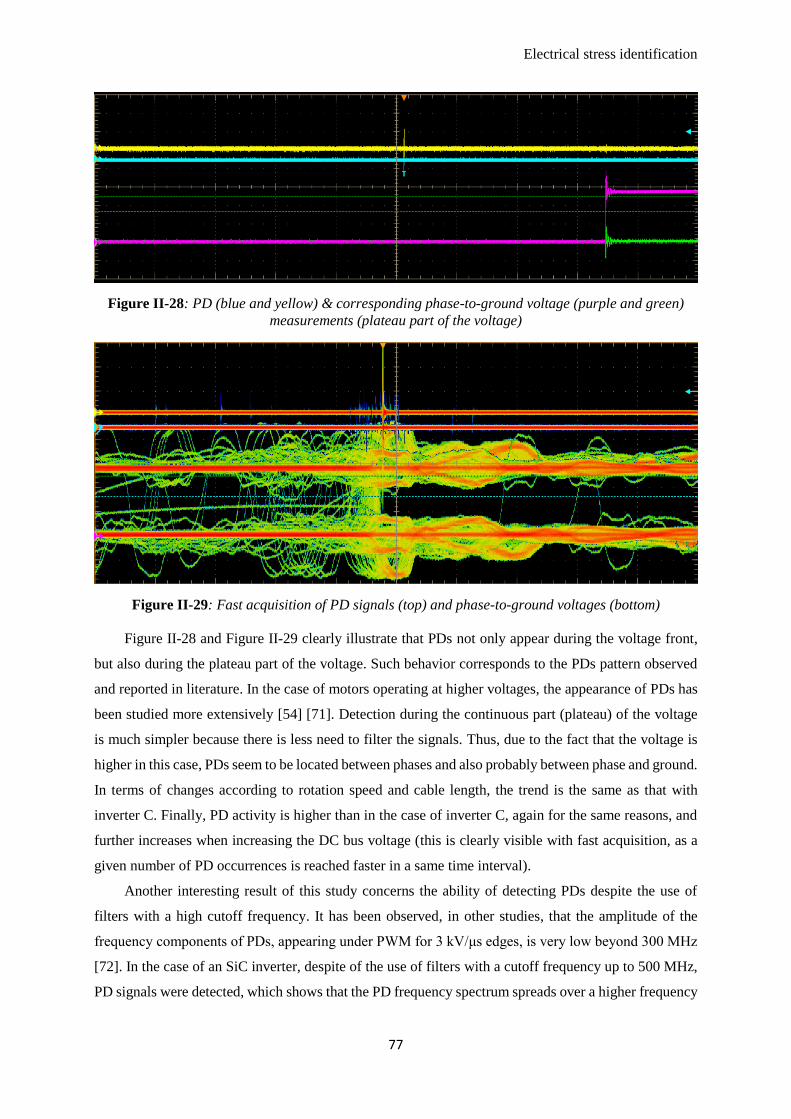
Electrical stress identification
77
Figure II-28: PD (blue and yellow) & corresponding phase-to-ground voltage (purple and green)
measurements (plateau part of the voltage)
Figure II-29: Fast acquisition of PD signals (top) and phase-to-ground voltages (bottom)
Figure II-28 and Figure II-29 clearly illustrate that PDs not only appear during the voltage front,
but also during the plateau part of the voltage. Such behavior corresponds to the PDs pattern observed
and reported in literature. In the case of motors operating at higher voltages, the appearance of PDs has
been studied more extensively [54] [71]. Detection during the continuous part (plateau) of the voltage
is much simpler because there is less need to filter the signals. Thus, due to the fact that the voltage is
higher in this case, PDs seem to be located between phases and also probably between phase and ground.
In terms of changes according to rotation speed and cable length, the trend is the same as that with
inverter C. Finally, PD activity is higher than in the case of inverter C, again for the same reasons, and
further increases when increasing the DC bus voltage (this is clearly visible with fast acquisition, as a
given number of PD occurrences is reached faster in a same time interval).
Another interesting result of this study concerns the ability of detecting PDs despite the use of
filters with a high cutoff frequency. It has been observed, in other studies, that the amplitude of the
frequency components of PDs, appearing under PWM for 3 kV/μs edges, is very low beyond 300 MHz
[72]. In the case of an SiC inverter, despite of the use of filters with a cutoff frequency up to 500 MHz,
PD signals were detected, which shows that the PD frequency spectrum spreads over a higher frequency
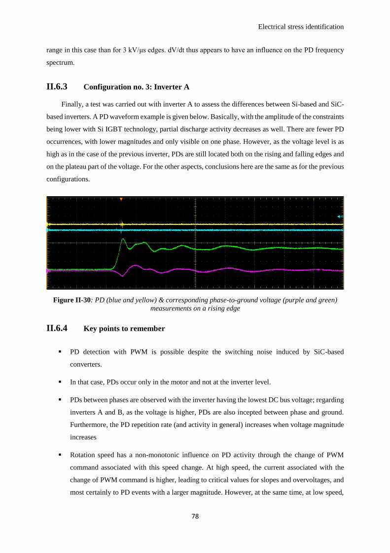
Electrical stress identification
78
range in this case than for 3 kV/μs edges. dV/dt thus appears to have an influence on the PD frequency
spectrum.
II.6.3 Configuration no. 3: Inverter A
Finally, a test was carried out with inverter A to assess the differences between Si-based and SiC-
based inverters. A PD waveform example is given below. Basically, with the amplitude of the constraints
being lower with Si IGBT technology, partial discharge activity decreases as well. There are fewer PD
occurrences, with lower magnitudes and only visible on one phase. However, as the voltage level is as
high as in the case of the previous inverter, PDs are still located both on the rising and falling edges and
on the plateau part of the voltage. For the other aspects, conclusions here are the same as for the previous
configurations.
Figure II-30: PD (blue and yellow) & corresponding phase-to-ground voltage (purple and green)
measurements on a rising edge
II.6.4 Key points to remember
PD detection with PWM is possible despite the switching noise induced by SiC-based
converters.
In that case, PDs occur only in the motor and not at the inverter level.
PDs between phases are observed with the inverter having the lowest DC bus voltage; regarding
inverters A and B, as the voltage is higher, PDs are also incepted between phase and ground.
Furthermore, the PD repetition rate (and activity in general) increases when voltage magnitude
increases
Rotation speed has a non-monotonic influence on PD activity through the change of PWM
command associated with this speed change. At high speed, the current associated with the
change of PWM command is higher, leading to critical values for slopes and overvoltages, and
most certainly to PD events with a larger magnitude. However, at the same time, at low speed,

Electrical stress identification
79
the current is lower but there is a large number of switching occurrences, and thus possibly an
increased number of PDs. It is thus difficult to rule on the precise impact of the rotation speed
on PD activity.
Cable length has little influence on PDs, or at least influence that is difficult to quantify; in most
of cases, the voltage slope shows little change when the cable length is modified, and the voltage
increase is not large enough to induce significant modifications in PD activity.
At high voltage, PDs are not only observed on the rising edges but also on the plateau part of
the voltage.
dV/dt has an influence on the PD frequency spectrum.
The transition to SiC-based components increases PD activity.
Electrical stress identification
80
II.7 Conclusion
This chapter identified the electrical stresses in a machine supplied by Si-based and SiC-based
inverters. By using a custom-made experimental bench, we were able to study the influence of various
parameters related to the power chain and, on the basis of those results, to obtain insight regarding the
turn-to-turn, phase-to-ground, and phase-to-phase voltages in the machine. Furthermore, PD
measurements were performed as a complement to this electrical stress mapping to highlight the direct
impact of these more stressful constraints on machine reliability, and high voltage machines in general.
In Type I random-wound motors, partial discharges appear because of the combined effects of
random winding with a large number of turns, propagation phenomena, and rising edges. In Type II
motors, winding is formed and composed of few turns. We have seen that the turn-to-turn voltage values
are low in this type of motor. Given these voltages, power electronics and thus rising edge propagation
can have little influence on the ignition of partial discharges between turns. Nevertheless, the use of fast-
switching SiC-based inverters causes an increase of overvoltages for phase-to-ground and phase-to-
phase voltages. Therefore, these insulation systems constitute the weakest point of the system in terms
of reliability. These overvoltages are mainly induced due to propagation phenomena between the
inverter and the motor, but they also depend on numerous internal and external parameters, such as
switched current, rotation speed, and cable length. These more stressful constraints eventually lead to
an increase in partial discharge activity between phases or between phase and ground. For this reason,
such electrical stress mapping under operating conditions is one of the key building blocks for achieving
better understanding [73], reproduction [74], detection [11], and monitoring [37] of the phenomenon.
The next step in this work is now to establish a correlation between electrical stress and partial
discharge activity. A first step was taken with PD measurements performed on the machine, but that
only enables us to obtain a broad vision of PD activity inside the machine. Now that the electrical stresses
inside the machine are well known, a detailed study on the influence of every component of these voltage
stresses in terms of PDs and aging must be performed. This will be examined in the following part of
our work, notably by performing PD measurements and running accelerated aging on representative
samples from simple Type I samples to more complex Type II insulation systems.

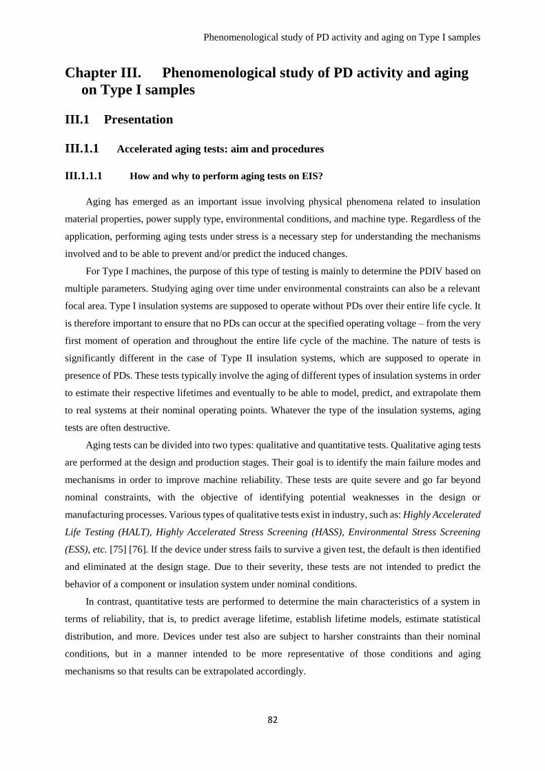
Phenomenological study of PD activity and aging on Type I samples
82
Chapter III. Phenomenological study of PD activity and aging
on Type I samples
III.1 Presentation
III.1.1 Accelerated aging tests: aim and procedures
III.1.1.1 How and why to perform aging tests on EIS?
Aging has emerged as an important issue involving physical phenomena related to insulation
material properties, power supply type, environmental conditions, and machine type. Regardless of the
application, performing aging tests under stress is a necessary step for understanding the mechanisms
involved and to be able to prevent and/or predict the induced changes.
For Type I machines, the purpose of this type of testing is mainly to determine the PDIV based on
multiple parameters. Studying aging over time under environmental constraints can also be a relevant
focal area. Type I insulation systems are supposed to operate without PDs over their entire life cycle. It
is therefore important to ensure that no PDs can occur at the specified operating voltage – from the very
first moment of operation and throughout the entire life cycle of the machine. The nature of tests is
significantly different in the case of Type II insulation systems, which are supposed to operate in
presence of PDs. These tests typically involve the aging of different types of insulation systems in order
to estimate their respective lifetimes and eventually to be able to model, predict, and extrapolate them
to real systems at their nominal operating points. Whatever the type of the insulation systems, aging
tests are often destructive.
Aging tests can be divided into two types: qualitative and quantitative tests. Qualitative aging tests
are performed at the design and production stages. Their goal is to identify the main failure modes and
mechanisms in order to improve machine reliability. These tests are quite severe and go far beyond
nominal constraints, with the objective of identifying potential weaknesses in the design or
manufacturing processes. Various types of qualitative tests exist in industry, such as: Highly Accelerated
Life Testing (HALT), Highly Accelerated Stress Screening (HASS), Environmental Stress Screening
(ESS), etc. [75] [76]. If the device under stress fails to survive a given test, the default is then identified
and eliminated at the design stage. Due to their severity, these tests are not intended to predict the
behavior of a component or insulation system under nominal conditions.
In contrast, quantitative tests are performed to determine the main characteristics of a system in
terms of reliability, that is, to predict average lifetime, establish lifetime models, estimate statistical
distribution, and more. Devices under test also are subject to harsher constraints than their nominal
conditions, but in a manner intended to be more representative of those conditions and aging
mechanisms so that results can be extrapolated accordingly.
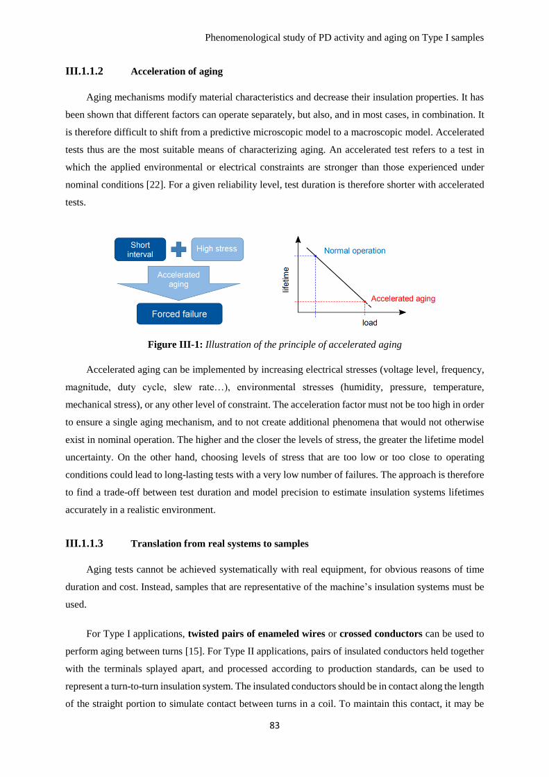
Phenomenological study of PD activity and aging on Type I samples
83
III.1.1.2 Acceleration of aging
Aging mechanisms modify material characteristics and decrease their insulation properties. It has
been shown that different factors can operate separately, but also, and in most cases, in combination. It
is therefore difficult to shift from a predictive microscopic model to a macroscopic model. Accelerated
tests thus are the most suitable means of characterizing aging. An accelerated test refers to a test in
which the applied environmental or electrical constraints are stronger than those experienced under
nominal conditions [22]. For a given reliability level, test duration is therefore shorter with accelerated
tests.
Figure III-1: Illustration of the principle of accelerated aging
Accelerated aging can be implemented by increasing electrical stresses (voltage level, frequency,
magnitude, duty cycle, slew rate…), environmental stresses (humidity, pressure, temperature,
mechanical stress), or any other level of constraint. The acceleration factor must not be too high in order
to ensure a single aging mechanism, and to not create additional phenomena that would not otherwise
exist in nominal operation. The higher and the closer the levels of stress, the greater the lifetime model
uncertainty. On the other hand, choosing levels of stress that are too low or too close to operating
conditions could lead to long-lasting tests with a very low number of failures. The approach is therefore
to find a trade-off between test duration and model precision to estimate insulation systems lifetimes
accurately in a realistic environment.
III.1.1.3 Translation from real systems to samples
Aging tests cannot be achieved systematically with real equipment, for obvious reasons of time
duration and cost. Instead, samples that are representative of the machine’s insulation systems must be
used.
For Type I applications, twisted pairs of enameled wires or crossed conductors can be used to
perform aging between turns [15]. For Type II applications, pairs of insulated conductors held together
with the terminals splayed apart, and processed according to production standards, can be used to
represent a turn-to-turn insulation system. The insulated conductors should be in contact along the length
of the straight portion to simulate contact between turns in a coil. To maintain this contact, it may be
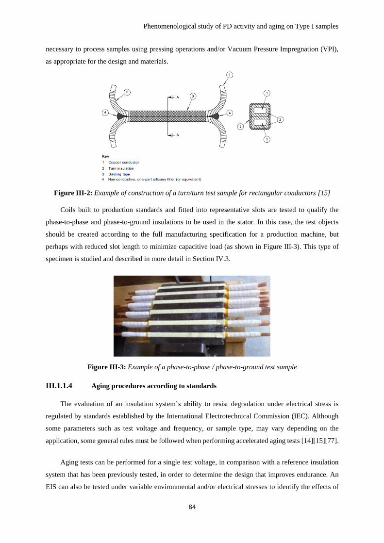
Phenomenological study of PD activity and aging on Type I samples
84
necessary to process samples using pressing operations and/or Vacuum Pressure Impregnation (VPI),
as appropriate for the design and materials.
Figure III-2: Example of construction of a turn/turn test sample for rectangular conductors [15]
Coils built to production standards and fitted into representative slots are tested to qualify the
phase-to-phase and phase-to-ground insulations to be used in the stator. In this case, the test objects
should be created according to the full manufacturing specification for a production machine, but
perhaps with reduced slot length to minimize capacitive load (as shown in Figure III-3). This type of
specimen is studied and described in more detail in Section IV.3.
Figure III-3: Example of a phase-to-phase / phase-to-ground test sample
III.1.1.4 Aging procedures according to standards
The evaluation of an insulation system’s ability to resist degradation under electrical stress is
regulated by standards established by the International Electrotechnical Commission (IEC). Although
some parameters such as test voltage and frequency, or sample type, may vary depending on the
application, some general rules must be followed when performing accelerated aging tests [14][15][77].
Aging tests can be performed for a single test voltage, in comparison with a reference insulation
system that has been previously tested, in order to determine the design that improves endurance. An
EIS can also be tested under variable environmental and/or electrical stresses to identify the effects of
Phenomenological study of PD activity and aging on Type I samples
85
those various factors. Finally, endurance tests can be carried out to evaluate the relationship between
applied voltage and lifetime for each insulation system. It is customary to only vary one constraint at a
time to segregate and interpret results effectively. The results of these tests depend on multiple
parameters which must be clearly identified and controlled, in addition to the insulation’s intrinsic
characteristics.
The Device Under Test (DUT) must be suitable for the application scope. A larger number of
samples must be considered if high statistical precision is needed to detect small differences. It is
preferable to use at least five samples per stress level to obtain the minimum requirement in terms of
precision. Test results must then be processed statistically using one of the distributions presented in
Section I.5.1.2. On the basis of shape and scale parameter estimation, the MTTF (Mean Time To
Failure), number of pulses before breakdown, and percentage of failures can be determined. Confidence
intervals for parameters and percentages can also be calculated. 90% probability is recommended.
PDIV and PDEV must be determined prior to testing. For impulse voltage, it is common practice
to rather consider RPDIV and RPDEV (Repetitive Partial Discharge Inception/ Extinction Voltage), that
is, the minimum peak-to-peak voltage at which more than five PD pulses occur on ten voltage impulses
of the same polarity (note: this is a mean value for the specified test time and a test arrangement where
the voltage applied to the test object is gradually increased from a value at which no partial discharges
can be detected). The operating conditions and at least three levels of voltages above this threshold must
be chosen to perform tests, with a difference of at least 10% between two consecutive levels. Finally,
the degradation mechanism must be the same across the full range of voltages and similar to those
encountered under operating conditions.
For the sake of brevity here, the above recommendations are included in the specifications
advocated by the different standards. For more information, please refer to the IEC 60034-18-41[14],
IEC 60034-18-42 [15], IEC 60851-5 [78], and IEC 62068 [77] standards, to name but a few.
III.1.2 Purpose of this study
The first step of this study overall was dedicated to identifying the electrical stress inside a machine
supplied by Si IGBT and SiC MOSFET based inverters, in order to have clear insight regarding the risk
for Type II machines depending on various parameters. Building on this preliminary work, the aim of
the following parts is now to understand the influence of relevant constraints on partial discharge activity
and, in the longer term, on the aging of the machine’s insulation systems. To move forward, a three-
stage approach was adopted based on samples ranging from the simplest Type I sample to more
sophisticated systems closer to a real Type II machine.
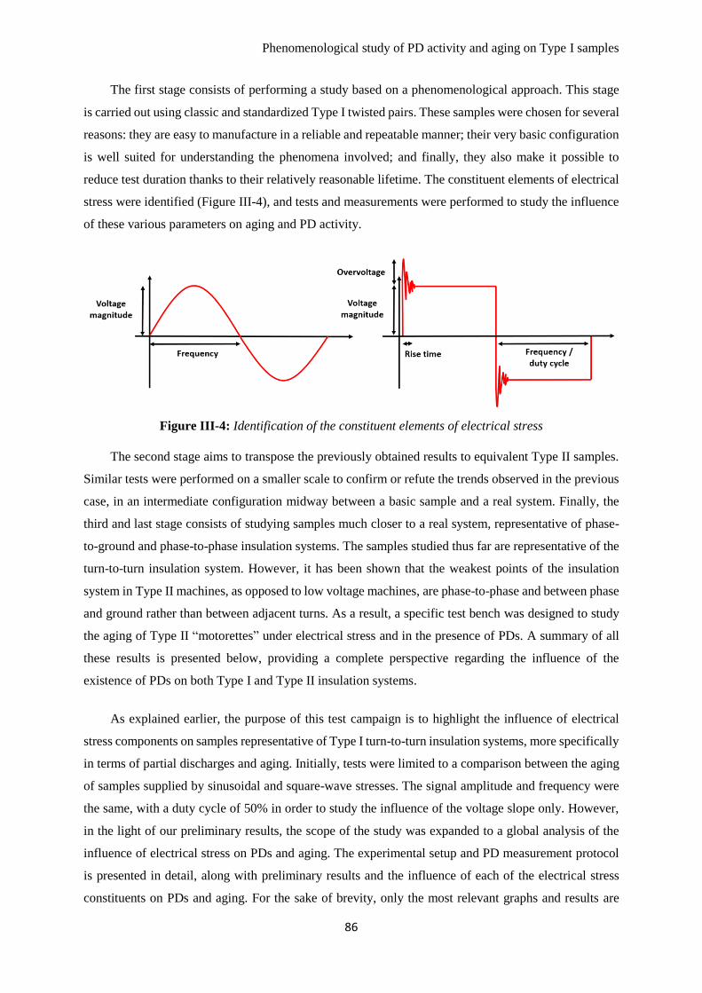
Phenomenological study of PD activity and aging on Type I samples
86
The first stage consists of performing a study based on a phenomenological approach. This stage
is carried out using classic and standardized Type I twisted pairs. These samples were chosen for several
reasons: they are easy to manufacture in a reliable and repeatable manner; their very basic configuration
is well suited for understanding the phenomena involved; and finally, they also make it possible to
reduce test duration thanks to their relatively reasonable lifetime. The constituent elements of electrical
stress were identified (Figure III-4), and tests and measurements were performed to study the influence
of these various parameters on aging and PD activity.
Figure III-4: Identification of the constituent elements of electrical stress
The second stage aims to transpose the previously obtained results to equivalent Type II samples.
Similar tests were performed on a smaller scale to confirm or refute the trends observed in the previous
case, in an intermediate configuration midway between a basic sample and a real system. Finally, the
third and last stage consists of studying samples much closer to a real system, representative of phase-
to-ground and phase-to-phase insulation systems. The samples studied thus far are representative of the
turn-to-turn insulation system. However, it has been shown that the weakest points of the insulation
system in Type II machines, as opposed to low voltage machines, are phase-to-phase and between phase
and ground rather than between adjacent turns. As a result, a specific test bench was designed to study
the aging of Type II “motorettes” under electrical stress and in the presence of PDs. A summary of all
these results is presented below, providing a complete perspective regarding the influence of the
existence of PDs on both Type I and Type II insulation systems.
As explained earlier, the purpose of this test campaign is to highlight the influence of electrical
stress components on samples representative of Type I turn-to-turn insulation systems, more specifically
in terms of partial discharges and aging. Initially, tests were limited to a comparison between the aging
of samples supplied by sinusoidal and square-wave stresses. The signal amplitude and frequency were
the same, with a duty cycle of 50% in order to study the influence of the voltage slope only. However,
in the light of our preliminary results, the scope of the study was expanded to a global analysis of the
influence of electrical stress on PDs and aging. The experimental setup and PD measurement protocol
is presented in detail, along with preliminary results and the influence of each of the electrical stress
constituents on PDs and aging. For the sake of brevity, only the most relevant graphs and results are
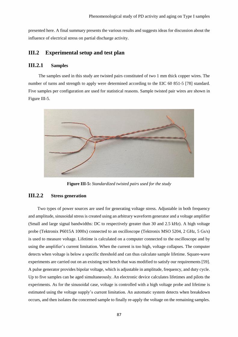
Phenomenological study of PD activity and aging on Type I samples
87
presented here. A final summary presents the various results and suggests ideas for discussion about the
influence of electrical stress on partial discharge activity.
III.2 Experimental setup and test plan
III.2.1 Samples
The samples used in this study are twisted pairs constituted of two 1 mm thick copper wires. The
number of turns and strength to apply were determined according to the EIC 60 851-5 [78] standard.
Five samples per configuration are used for statistical reasons. Sample twisted pair wires are shown in
Figure III-5.
Figure III-5: Standardized twisted pairs used for the study
III.2.2 Stress generation
Two types of power sources are used for generating voltage stress. Adjustable in both frequency
and amplitude, sinusoidal stress is created using an arbitrary waveform generator and a voltage amplifier
(Small and large signal bandwidths: DC to respectively greater than 30 and 2.5 kHz). A high voltage
probe (Tektronix P6015A 1000x) connected to an oscilloscope (Tektronix MSO 5204, 2 GHz, 5 Gs/s)
is used to measure voltage. Lifetime is calculated on a computer connected to the oscilloscope and by
using the amplifier’s current limitation. When the current is too high, voltage collapses. The computer
detects when voltage is below a specific threshold and can thus calculate sample lifetime. Square-wave
experiments are carried out on an existing test bench that was modified to satisfy our requirements [59].
A pulse generator provides bipolar voltage, which is adjustable in amplitude, frequency, and duty cycle.
Up to five samples can be aged simultaneously. An electronic device calculates lifetimes and pilots the
experiments. As for the sinusoidal case, voltage is controlled with a high voltage probe and lifetime is
estimated using the voltage supply’s current limitation. An automatic system detects when breakdown
occurs, and then isolates the concerned sample to finally re-apply the voltage on the remaining samples.
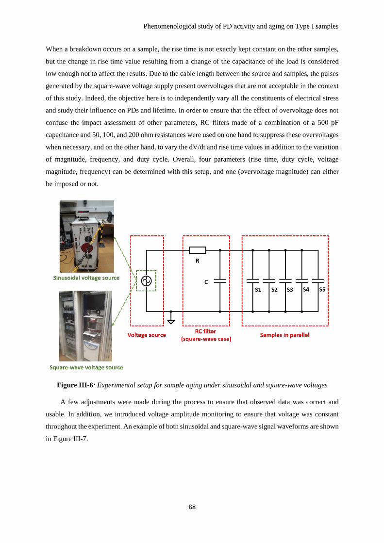
Phenomenological study of PD activity and aging on Type I samples
88
When a breakdown occurs on a sample, the rise time is not exactly kept constant on the other samples,
but the change in rise time value resulting from a change of the capacitance of the load is considered
low enough not to affect the results. Due to the cable length between the source and samples, the pulses
generated by the square-wave voltage supply present overvoltages that are not acceptable in the context
of this study. Indeed, the objective here is to independently vary all the constituents of electrical stress
and study their influence on PDs and lifetime. In order to ensure that the effect of overvoltage does not
confuse the impact assessment of other parameters, RC filters made of a combination of a 500 pF
capacitance and 50, 100, and 200 ohm resistances were used on one hand to suppress these overvoltages
when necessary, and on the other hand, to vary the dV/dt and rise time values in addition to the variation
of magnitude, frequency, and duty cycle. Overall, four parameters (rise time, duty cycle, voltage
magnitude, frequency) can be determined with this setup, and one (overvoltage magnitude) can either
be imposed or not.
Figure III-6: Experimental setup for sample aging under sinusoidal and square-wave voltages
A few adjustments were made during the process to ensure that observed data was correct and
usable. In addition, we introduced voltage amplitude monitoring to ensure that voltage was constant
throughout the experiment. An example of both sinusoidal and square-wave signal waveforms are shown
in Figure III-7.
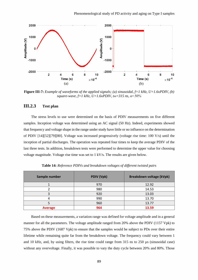
Phenomenological study of PD activity and aging on Type I samples
89
Figure III-7: Example of waveforms of the applied signals; (a) sinusoidal, f=1 kHz, U=1.6xPDIV, (b)
square-wave, f=1 kHz, U=1.6xPDIV, tm=315 ns, α=50%
III.2.3 Test plan
The stress levels to use were determined on the basis of PDIV measurements on five different
samples. Inception voltage was determined using an AC signal (50 Hz). Indeed, experiments showed
that frequency and voltage shape in the range under study have little or no influence on the determination
of PDIV [14][52][79][80]. Voltage was increased progressively (voltage rise time: 100 V/s) until the
inception of partial discharges. The operation was repeated four times to keep the average PDIV of the
last three tests. In addition, breakdown tests were performed to determine the upper value for choosing
voltage magnitude. Voltage rise time was set to 1 kV/s. The results are given below.
Table 14: Reference PDIVs and breakdown voltages of different twisted pairs
Sample number PDIV (Vpk) Breakdown voltage (kVpk)
1 970 12.92
2 980 14.53
3 920 13.03
4 990 13.70
5 960 13.77
Average 964 13.59
Based on these measurements, a variation range was defined for voltage amplitude and in a general
manner for all the parameters. The voltage amplitude ranged from 20% above the PDIV (1157 Vpk) to
75% above the PDIV (1687 Vpk) to ensure that the samples would be subject to PDs over their entire
lifetime while remaining quite far from the breakdown voltage. The frequency could vary between 1
and 10 kHz, and, by using filters, the rise time could range from 315 ns to 250 µs (sinusoidal case)
without any overvoltage. Finally, it was possible to vary the duty cycle between 20% and 80%. Those
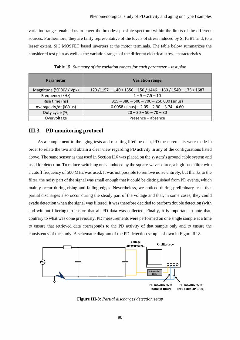
Phenomenological study of PD activity and aging on Type I samples
90
variation ranges enabled us to cover the broadest possible spectrum within the limits of the different
sources. Furthermore, they are fairly representative of the levels of stress induced by Si IGBT and, to a
lesser extent, SiC MOSFET based inverters at the motor terminals. The table below summarizes the
considered test plan as well as the variation ranges of the different electrical stress characteristics.
Table 15: Summary of the variation ranges for each parameter – test plan
Parameter Variation range
Magnitude (%PDIV / Vpk) 120 /1157 – 140 / 1350 – 150 / 1446 – 160 / 1540 – 175 / 1687
Frequency (kHz) 1 – 5 – 7.5 – 10
Rise time (ns) 315 – 380 – 500 – 700 – 250 000 (sinus)
Average dV/dt (kV/µs) 0.0058 (sinus) – 2.05 – 2.90 – 3.74 - 4.60
Duty cycle (%) 20 – 30 – 50 – 70 – 80
Overvoltage Presence – absence
III.3 PD monitoring protocol
As a complement to the aging tests and resulting lifetime data, PD measurements were made in
order to relate the two and obtain a clear view regarding PD activity in any of the configurations listed
above. The same sensor as that used in Section II.6 was placed on the system’s ground cable system and
used for detection. To reduce switching noise induced by the square-wave source, a high-pass filter with
a cutoff frequency of 500 MHz was used. It was not possible to remove noise entirely, but thanks to the
filter, the noisy part of the signal was small enough that it could be distinguished from PD events, which
mainly occur during rising and falling edges. Nevertheless, we noticed during preliminary tests that
partial discharges also occur during the steady part of the voltage and that, in some cases, they could
evade detection when the signal was filtered. It was therefore decided to perform double detection (with
and without filtering) to ensure that all PD data was collected. Finally, it is important to note that,
contrary to what was done previously, PD measurements were performed on one single sample at a time
to ensure that retrieved data corresponds to the PD activity of that sample only and to ensure the
consistency of the study. A schematic diagram of the PD detection setup is shown in Figure III-8.
Figure III-8: Partial discharges detection setup
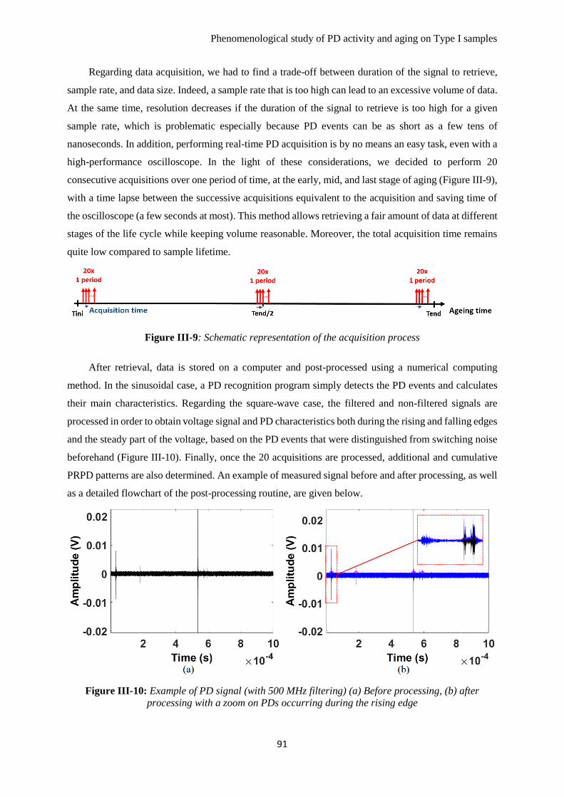
Phenomenological study of PD activity and aging on Type I samples
91
Regarding data acquisition, we had to find a trade-off between duration of the signal to retrieve,
sample rate, and data size. Indeed, a sample rate that is too high can lead to an excessive volume of data.
At the same time, resolution decreases if the duration of the signal to retrieve is too high for a given
sample rate, which is problematic especially because PD events can be as short as a few tens of
nanoseconds. In addition, performing real-time PD acquisition is by no means an easy task, even with a
high-performance oscilloscope. In the light of these considerations, we decided to perform 20
consecutive acquisitions over one period of time, at the early, mid, and last stage of aging (Figure III-9),
with a time lapse between the successive acquisitions equivalent to the acquisition and saving time of
the oscilloscope (a few seconds at most). This method allows retrieving a fair amount of data at different
stages of the life cycle while keeping volume reasonable. Moreover, the total acquisition time remains
quite low compared to sample lifetime.
Figure III-9: Schematic representation of the acquisition process
After retrieval, data is stored on a computer and post-processed using a numerical computing
method. In the sinusoidal case, a PD recognition program simply detects the PD events and calculates
their main characteristics. Regarding the square-wave case, the filtered and non-filtered signals are
processed in order to obtain voltage signal and PD characteristics both during the rising and falling edges
and the steady part of the voltage, based on the PD events that were distinguished from switching noise
beforehand (Figure III-10). Finally, once the 20 acquisitions are processed, additional and cumulative
PRPD patterns are also determined. An example of measured signal before and after processing, as well
as a detailed flowchart of the post-processing routine, are given below.
Figure III-10: Example of PD signal (with 500 MHz filtering) (a) Before processing, (b) after
processing with a zoom on PDs occurring during the rising edge
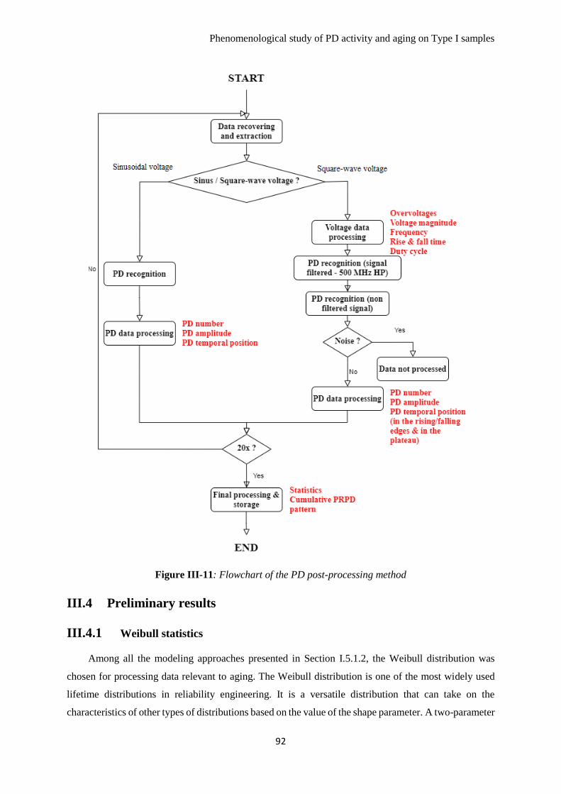
Phenomenological study of PD activity and aging on Type I samples
92
Figure III-11: Flowchart of the PD post-processing method
III.4 Preliminary results
III.4.1 Weibull statistics
Among all the modeling approaches presented in Section I.5.1.2, the Weibull distribution was
chosen for processing data relevant to aging. The Weibull distribution is one of the most widely used
lifetime distributions in reliability engineering. It is a versatile distribution that can take on the
characteristics of other types of distributions based on the value of the shape parameter. A two-parameter
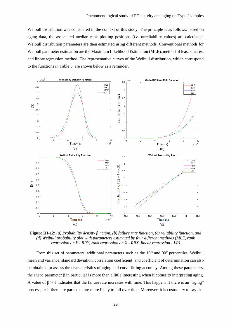
Phenomenological study of PD activity and aging on Type I samples
93
Weibull distribution was considered in the context of this study. The principle is as follows: based on
aging data, the associated median rank plotting positions (i.e. unreliability values) are calculated.
Weibull distribution parameters are then estimated using different methods. Conventional methods for
Weibull parameter estimation are the Maximum Likelihood Estimation (MLE), method of least squares,
and linear regression method. The representative curves of the Weibull distribution, which correspond
to the functions in Table 5, are shown below as a reminder.
Figure III-12: (a) Probability density function, (b) failure rate function, (c) reliability function, and
(d) Weibull probability plot with parameters estimated by four different methods (MLE, rank
regression on Y - RRY, rank regression on X - RRX, linear regression - LR)
From this set of parameters, additional parameters such as the 10th and 90th percentiles, Weibull
mean and variance, standard deviation, correlation coefficient, and coefficient of determination can also
be obtained to assess the characteristics of aging and curve fitting accuracy. Among these parameters,
the shape parameter β in particular is more than a little interesting when it comes to interpreting aging.
A value of β > 1 indicates that the failure rate increases with time. This happens if there is an “aging”
process, or if there are parts that are more likely to fail over time. Moreover, it is customary to say that
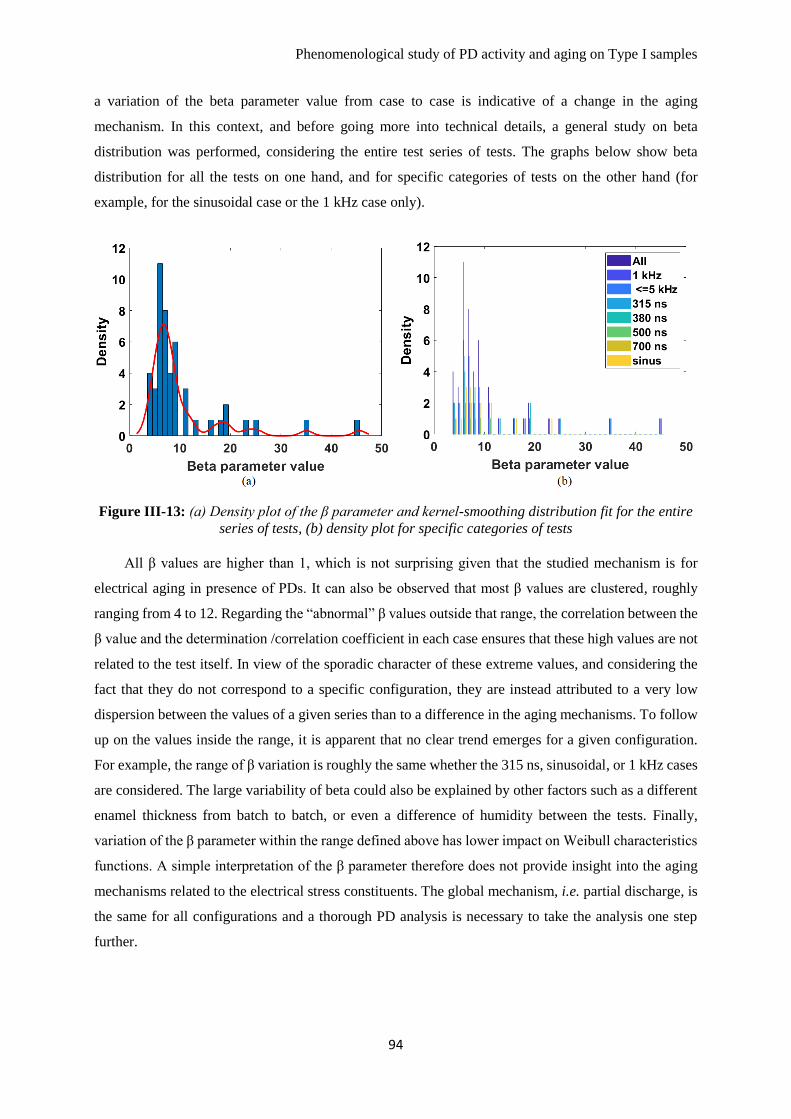
Phenomenological study of PD activity and aging on Type I samples
94
a variation of the beta parameter value from case to case is indicative of a change in the aging
mechanism. In this context, and before going more into technical details, a general study on beta
distribution was performed, considering the entire test series of tests. The graphs below show beta
distribution for all the tests on one hand, and for specific categories of tests on the other hand (for
example, for the sinusoidal case or the 1 kHz case only).
Figure III-13: (a) Density plot of the β parameter and kernel-smoothing distribution fit for the entire
series of tests, (b) density plot for specific categories of tests
All β values are higher than 1, which is not surprising given that the studied mechanism is for
electrical aging in presence of PDs. It can also be observed that most β values are clustered, roughly
ranging from 4 to 12. Regarding the “abnormal” β values outside that range, the correlation between the
β value and the determination /correlation coefficient in each case ensures that these high values are not
related to the test itself. In view of the sporadic character of these extreme values, and considering the
fact that they do not correspond to a specific configuration, they are instead attributed to a very low
dispersion between the values of a given series than to a difference in the aging mechanisms. To follow
up on the values inside the range, it is apparent that no clear trend emerges for a given configuration.
For example, the range of β variation is roughly the same whether the 315 ns, sinusoidal, or 1 kHz cases
are considered. The large variability of beta could also be explained by other factors such as a different
enamel thickness from batch to batch, or even a difference of humidity between the tests. Finally,
variation of the β parameter within the range defined above has lower impact on Weibull characteristics
functions. A simple interpretation of the β parameter therefore does not provide insight into the aging
mechanisms related to the electrical stress constituents. The global mechanism, i.e. partial discharge, is
the same for all configurations and a thorough PD analysis is necessary to take the analysis one step
further.
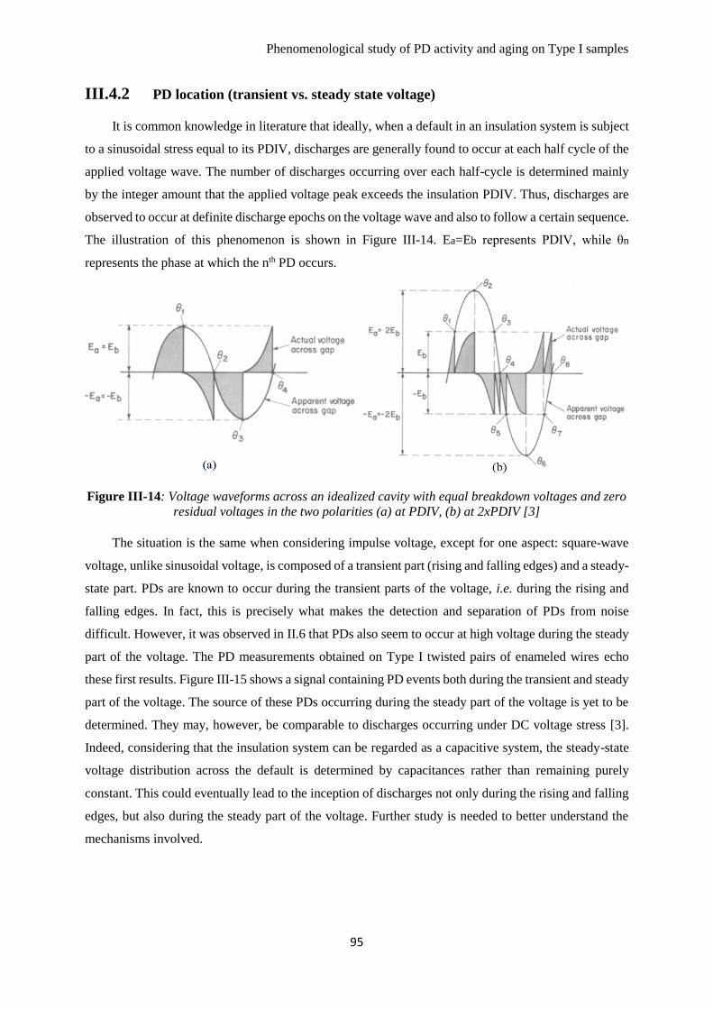
Phenomenological study of PD activity and aging on Type I samples
95
III.4.2 PD location (transient vs. steady state voltage)
It is common knowledge in literature that ideally, when a default in an insulation system is subject
to a sinusoidal stress equal to its PDIV, discharges are generally found to occur at each half cycle of the
applied voltage wave. The number of discharges occurring over each half-cycle is determined mainly
by the integer amount that the applied voltage peak exceeds the insulation PDIV. Thus, discharges are
observed to occur at definite discharge epochs on the voltage wave and also to follow a certain sequence.
The illustration of this phenomenon is shown in Figure III-14. Ea=Eb represents PDIV, while θn
represents the phase at which the nth PD occurs.
Figure III-14: Voltage waveforms across an idealized cavity with equal breakdown voltages and zero
residual voltages in the two polarities (a) at PDIV, (b) at 2xPDIV [3]
The situation is the same when considering impulse voltage, except for one aspect: square-wave
voltage, unlike sinusoidal voltage, is composed of a transient part (rising and falling edges) and a steady-
state part. PDs are known to occur during the transient parts of the voltage, i.e. during the rising and
falling edges. In fact, this is precisely what makes the detection and separation of PDs from noise
difficult. However, it was observed in II.6 that PDs also seem to occur at high voltage during the steady
part of the voltage. The PD measurements obtained on Type I twisted pairs of enameled wires echo
these first results. Figure III-15 shows a signal containing PD events both during the transient and steady
part of the voltage. The source of these PDs occurring during the steady part of the voltage is yet to be
determined. They may, however, be comparable to discharges occurring under DC voltage stress [3].
Indeed, considering that the insulation system can be regarded as a capacitive system, the steady-state
voltage distribution across the default is determined by capacitances rather than remaining purely
constant. This could eventually lead to the inception of discharges not only during the rising and falling
edges, but also during the steady part of the voltage. Further study is needed to better understand the
mechanisms involved.
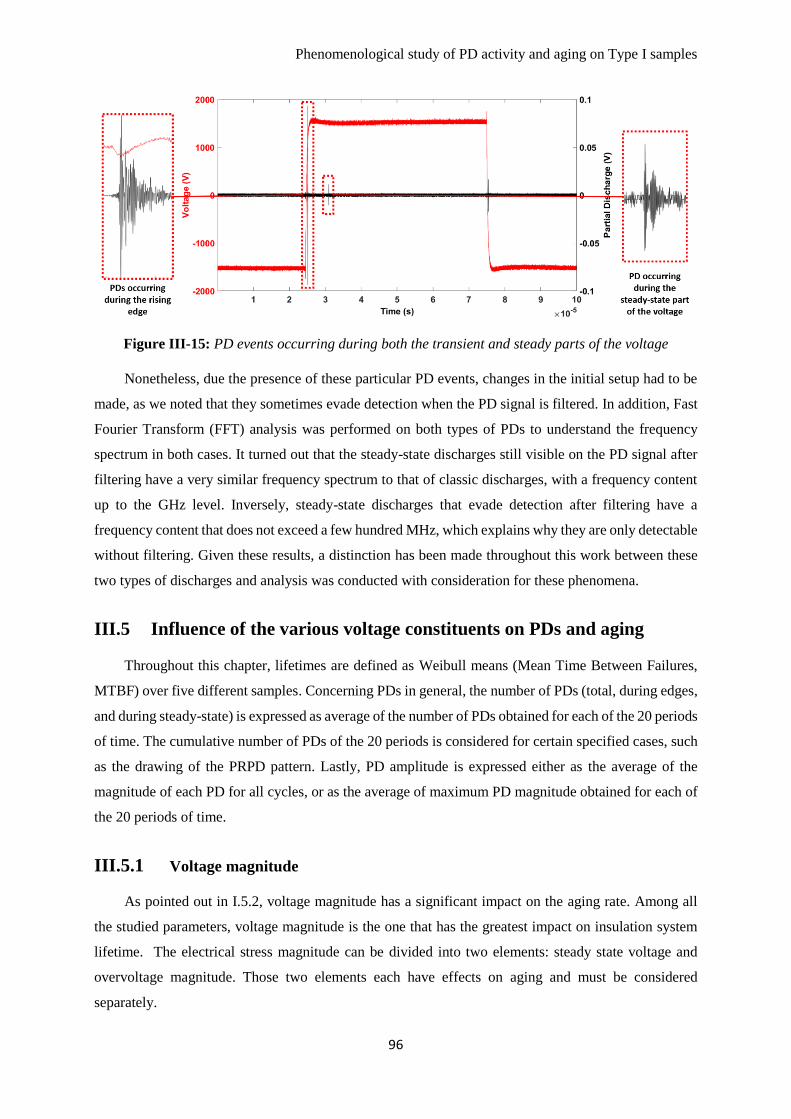
Phenomenological study of PD activity and aging on Type I samples
96
Figure III-15: PD events occurring during both the transient and steady parts of the voltage
Nonetheless, due the presence of these particular PD events, changes in the initial setup had to be
made, as we noted that they sometimes evade detection when the PD signal is filtered. In addition, Fast
Fourier Transform (FFT) analysis was performed on both types of PDs to understand the frequency
spectrum in both cases. It turned out that the steady-state discharges still visible on the PD signal after
filtering have a very similar frequency spectrum to that of classic discharges, with a frequency content
up to the GHz level. Inversely, steady-state discharges that evade detection after filtering have a
frequency content that does not exceed a few hundred MHz, which explains why they are only detectable
without filtering. Given these results, a distinction has been made throughout this work between these
two types of discharges and analysis was conducted with consideration for these phenomena.
III.5 Influence of the various voltage constituents on PDs and aging
Throughout this chapter, lifetimes are defined as Weibull means (Mean Time Between Failures,
MTBF) over five different samples. Concerning PDs in general, the number of PDs (total, during edges,
and during steady-state) is expressed as average of the number of PDs obtained for each of the 20 periods
of time. The cumulative number of PDs of the 20 periods is considered for certain specified cases, such
as the drawing of the PRPD pattern. Lastly, PD amplitude is expressed either as the average of the
magnitude of each PD for all cycles, or as the average of maximum PD magnitude obtained for each of
the 20 periods of time.
III.5.1 Voltage magnitude
As pointed out in I.5.2, voltage magnitude has a significant impact on the aging rate. Among all
the studied parameters, voltage magnitude is the one that has the greatest impact on insulation system
lifetime. The electrical stress magnitude can be divided into two elements: steady state voltage and
overvoltage magnitude. Those two elements each have effects on aging and must be considered
separately.
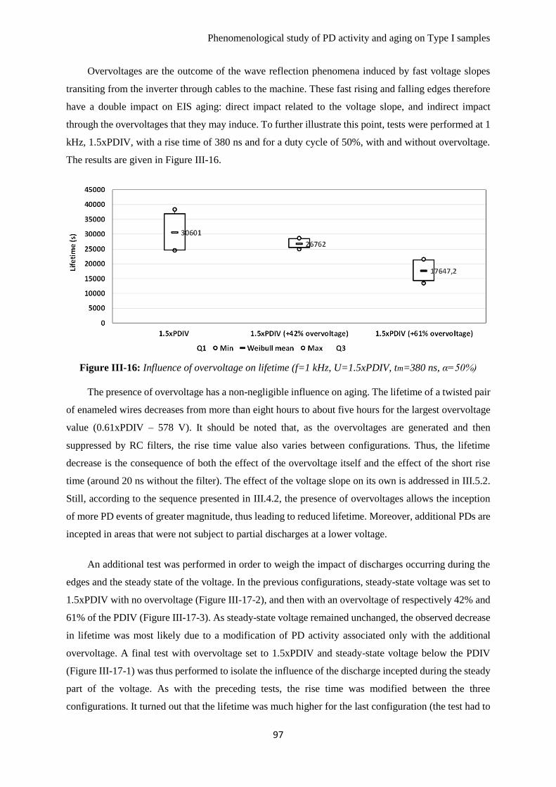
Phenomenological study of PD activity and aging on Type I samples
97
Overvoltages are the outcome of the wave reflection phenomena induced by fast voltage slopes
transiting from the inverter through cables to the machine. These fast rising and falling edges therefore
have a double impact on EIS aging: direct impact related to the voltage slope, and indirect impact
through the overvoltages that they may induce. To further illustrate this point, tests were performed at 1
kHz, 1.5xPDIV, with a rise time of 380 ns and for a duty cycle of 50%, with and without overvoltage.
The results are given in Figure III-16.
Figure III-16: Influence of overvoltage on lifetime (f=1 kHz, U=1.5xPDIV, tm=380 ns, α=50%)
The presence of overvoltage has a non-negligible influence on aging. The lifetime of a twisted pair
of enameled wires decreases from more than eight hours to about five hours for the largest overvoltage
value (0.61xPDIV – 578 V). It should be noted that, as the overvoltages are generated and then
suppressed by RC filters, the rise time value also varies between configurations. Thus, the lifetime
decrease is the consequence of both the effect of the overvoltage itself and the effect of the short rise
time (around 20 ns without the filter). The effect of the voltage slope on its own is addressed in III.5.2.
Still, according to the sequence presented in III.4.2, the presence of overvoltages allows the inception
of more PD events of greater magnitude, thus leading to reduced lifetime. Moreover, additional PDs are
incepted in areas that were not subject to partial discharges at a lower voltage.
An additional test was performed in order to weigh the impact of discharges occurring during the
edges and the steady state of the voltage. In the previous configurations, steady-state voltage was set to
1.5xPDIV with no overvoltage (Figure III-17-2), and then with an overvoltage of respectively 42% and
61% of the PDIV (Figure III-17-3). As steady-state voltage remained unchanged, the observed decrease
in lifetime was most likely due to a modification of PD activity associated only with the additional
overvoltage. A final test with overvoltage set to 1.5xPDIV and steady-state voltage below the PDIV
(Figure III-17-1) was thus performed to isolate the influence of the discharge incepted during the steady
part of the voltage. As with the preceding tests, the rise time was modified between the three
configurations. It turned out that the lifetime was much higher for the last configuration (the test had to
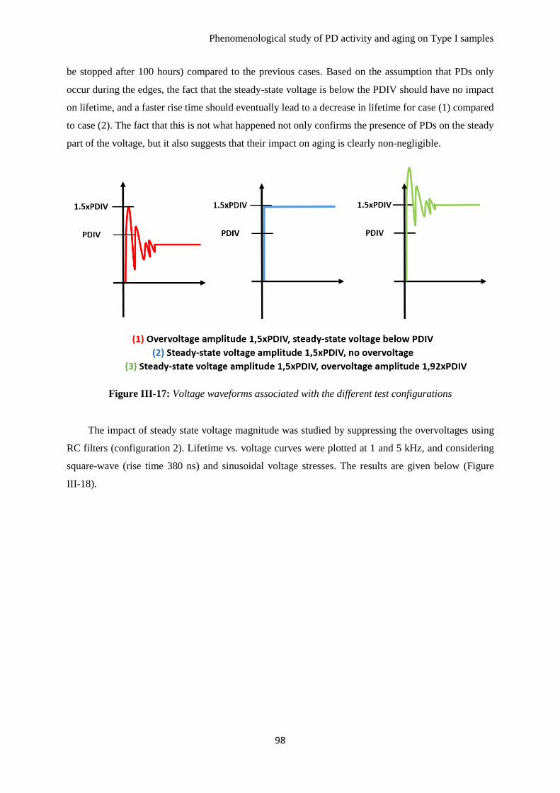
Phenomenological study of PD activity and aging on Type I samples
98
be stopped after 100 hours) compared to the previous cases. Based on the assumption that PDs only
occur during the edges, the fact that the steady-state voltage is below the PDIV should have no impact
on lifetime, and a faster rise time should eventually lead to a decrease in lifetime for case (1) compared
to case (2). The fact that this is not what happened not only confirms the presence of PDs on the steady
part of the voltage, but it also suggests that their impact on aging is clearly non-negligible.
Figure III-17: Voltage waveforms associated with the different test configurations
The impact of steady state voltage magnitude was studied by suppressing the overvoltages using
RC filters (configuration 2). Lifetime vs. voltage curves were plotted at 1 and 5 kHz, and considering
square-wave (rise time 380 ns) and sinusoidal voltage stresses. The results are given below (Figure
III-18).
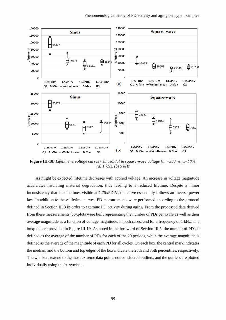
Phenomenological study of PD activity and aging on Type I samples
99
Figure III-18: Lifetime vs voltage curves - sinusoidal & square-wave voltage (tm=380 ns, α=50%)
(a) 1 kHz, (b) 5 kHz
As might be expected, lifetime decreases with applied voltage. An increase in voltage magnitude
accelerates insulating material degradation, thus leading to a reduced lifetime. Despite a minor
inconsistency that is sometimes visible at 1.75xPDIV, the curve essentially follows an inverse power
law. In addition to these lifetime curves, PD measurements were performed according to the protocol
defined in Section III.3 in order to examine PD activity during aging. From the processed data derived
from these measurements, boxplots were built representing the number of PDs per cycle as well as their
average magnitude as a function of voltage magnitude, in both cases, and for a frequency of 1 kHz. The
boxplots are provided in Figure III-19. As noted in the foreword of Section III.5, the number of PDs is
defined as the average of the number of PDs for each of the 20 periods, while the average magnitude is
defined as the average of the magnitude of each PD for all cycles. On each box, the central mark indicates
the median, and the bottom and top edges of the box indicate the 25th and 75th percentiles, respectively.
The whiskers extend to the most extreme data points not considered outliers, and the outliers are plotted
individually using the '+' symbol.
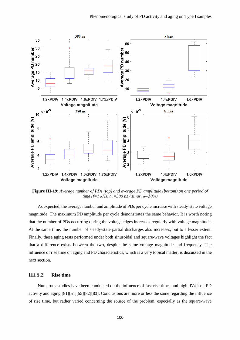
Phenomenological study of PD activity and aging on Type I samples
100
Figure III-19: Average number of PDs (top) and average PD amplitude (bottom) on one period of
time (f=1 kHz, tm=380 ns / sinus, α=50%)
As expected, the average number and amplitude of PDs per cycle increase with steady-state voltage
magnitude. The maximum PD amplitude per cycle demonstrates the same behavior. It is worth noting
that the number of PDs occurring during the voltage edges increases regularly with voltage magnitude.
At the same time, the number of steady-state partial discharges also increases, but to a lesser extent.
Finally, these aging tests performed under both sinusoidal and square-wave voltages highlight the fact
that a difference exists between the two, despite the same voltage magnitude and frequency. The
influence of rise time on aging and PD characteristics, which is a very topical matter, is discussed in the
next section.
III.5.2 Rise time
Numerous studies have been conducted on the influence of fast rise times and high dV/dt on PD
activity and aging [81][51][55][82][83]. Conclusions are more or less the same regarding the influence
of rise time, but rather varied concerning the source of the problem, especially as the square-wave
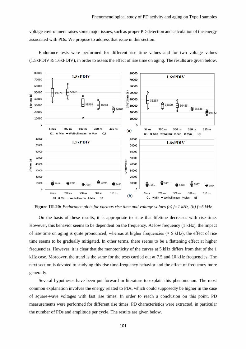
Phenomenological study of PD activity and aging on Type I samples
101
voltage environment raises some major issues, such as proper PD detection and calculation of the energy
associated with PDs. We propose to address that issue in this section.
Endurance tests were performed for different rise time values and for two voltage values
(1.5xPDIV & 1.6xPDIV), in order to assess the effect of rise time on aging. The results are given below.
Figure III-20: Endurance plots for various rise time and voltage values (a) f=1 kHz, (b) f=5 kHz
On the basis of these results, it is appropriate to state that lifetime decreases with rise time.
However, this behavior seems to be dependent on the frequency. At low frequency (1 kHz), the impact
of rise time on aging is quite pronounced; whereas at higher frequencies (≥ 5 kHz), the effect of rise
time seems to be gradually mitigated. In other terms, there seems to be a flattening effect at higher
frequencies. However, it is clear that the monotonicity of the curves at 5 kHz differs from that of the 1
kHz case. Moreover, the trend is the same for the tests carried out at 7.5 and 10 kHz frequencies. The
next section is devoted to studying this rise time-frequency behavior and the effect of frequency more
generally.
Several hypotheses have been put forward in literature to explain this phenomenon. The most
common explanation involves the energy related to PDs, which could supposedly be higher in the case
of square-wave voltages with fast rise times. In order to reach a conclusion on this point, PD
measurements were performed for different rise times. PD characteristics were extracted, in particular
the number of PDs and amplitude per cycle. The results are given below.
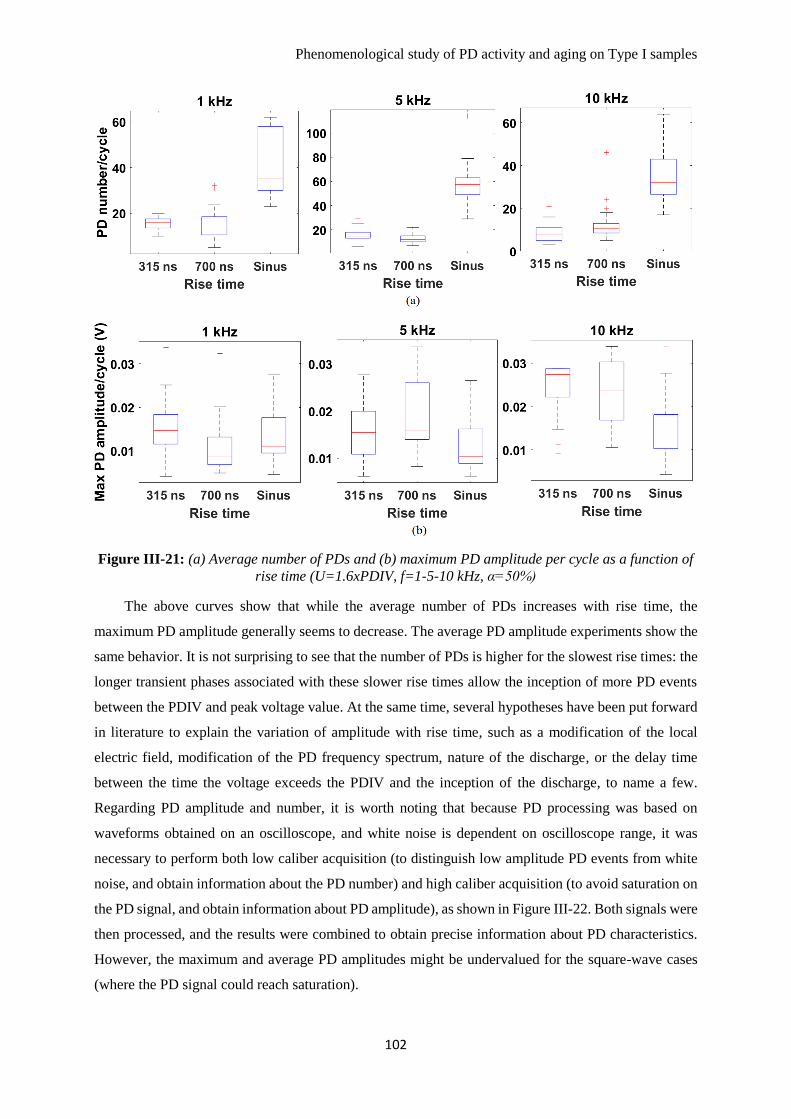
Phenomenological study of PD activity and aging on Type I samples
102
Figure III-21: (a) Average number of PDs and (b) maximum PD amplitude per cycle as a function of
rise time (U=1.6xPDIV, f=1-5-10 kHz, α=50%)
The above curves show that while the average number of PDs increases with rise time, the
maximum PD amplitude generally seems to decrease. The average PD amplitude experiments show the
same behavior. It is not surprising to see that the number of PDs is higher for the slowest rise times: the
longer transient phases associated with these slower rise times allow the inception of more PD events
between the PDIV and peak voltage value. At the same time, several hypotheses have been put forward
in literature to explain the variation of amplitude with rise time, such as a modification of the local
electric field, modification of the PD frequency spectrum, nature of the discharge, or the delay time
between the time the voltage exceeds the PDIV and the inception of the discharge, to name a few.
Regarding PD amplitude and number, it is worth noting that because PD processing was based on
waveforms obtained on an oscilloscope, and white noise is dependent on oscilloscope range, it was
necessary to perform both low caliber acquisition (to distinguish low amplitude PD events from white
noise, and obtain information about the PD number) and high caliber acquisition (to avoid saturation on
the PD signal, and obtain information about PD amplitude), as shown in Figure III-22. Both signals were
then processed, and the results were combined to obtain precise information about PD characteristics.
However, the maximum and average PD amplitudes might be undervalued for the square-wave cases
(where the PD signal could reach saturation).
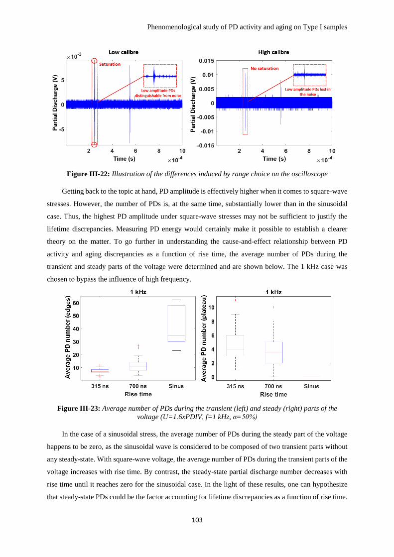
Phenomenological study of PD activity and aging on Type I samples
103
Figure III-22: Illustration of the differences induced by range choice on the oscilloscope
Getting back to the topic at hand, PD amplitude is effectively higher when it comes to square-wave
stresses. However, the number of PDs is, at the same time, substantially lower than in the sinusoidal
case. Thus, the highest PD amplitude under square-wave stresses may not be sufficient to justify the
lifetime discrepancies. Measuring PD energy would certainly make it possible to establish a clearer
theory on the matter. To go further in understanding the cause-and-effect relationship between PD
activity and aging discrepancies as a function of rise time, the average number of PDs during the
transient and steady parts of the voltage were determined and are shown below. The 1 kHz case was
chosen to bypass the influence of high frequency.
Figure III-23: Average number of PDs during the transient (left) and steady (right) parts of the
voltage (U=1.6xPDIV, f=1 kHz, α=50%)
In the case of a sinusoidal stress, the average number of PDs during the steady part of the voltage
happens to be zero, as the sinusoidal wave is considered to be composed of two transient parts without
any steady-state. With square-wave voltage, the average number of PDs during the transient parts of the
voltage increases with rise time. By contrast, the steady-state partial discharge number decreases with
rise time until it reaches zero for the sinusoidal case. In the light of these results, one can hypothesize
that steady-state PDs could be the factor accounting for lifetime discrepancies as a function of rise time.
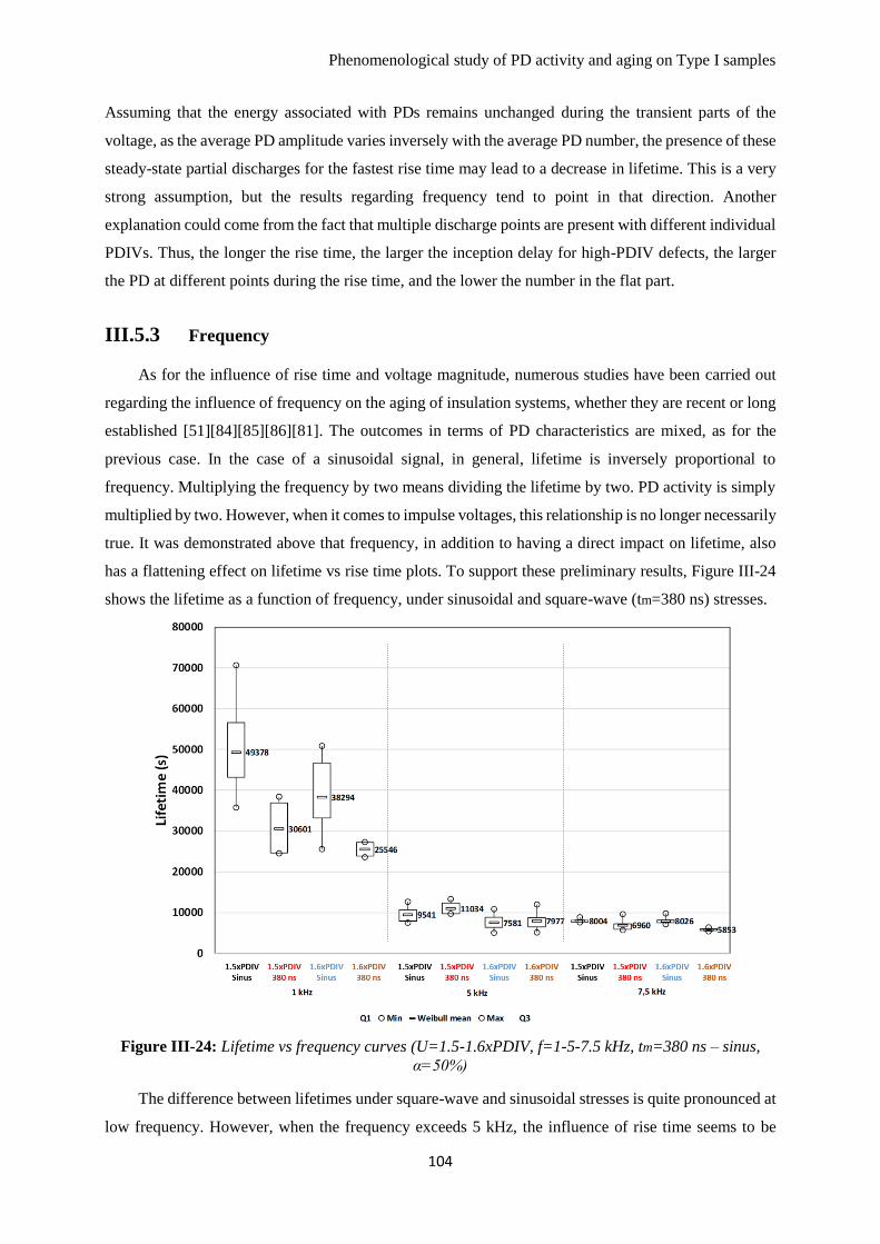
Phenomenological study of PD activity and aging on Type I samples
104
Assuming that the energy associated with PDs remains unchanged during the transient parts of the
voltage, as the average PD amplitude varies inversely with the average PD number, the presence of these
steady-state partial discharges for the fastest rise time may lead to a decrease in lifetime. This is a very
strong assumption, but the results regarding frequency tend to point in that direction. Another
explanation could come from the fact that multiple discharge points are present with different individual
PDIVs. Thus, the longer the rise time, the larger the inception delay for high-PDIV defects, the larger
the PD at different points during the rise time, and the lower the number in the flat part.
III.5.3 Frequency
As for the influence of rise time and voltage magnitude, numerous studies have been carried out
regarding the influence of frequency on the aging of insulation systems, whether they are recent or long
established [51][84][85][86][81]. The outcomes in terms of PD characteristics are mixed, as for the
previous case. In the case of a sinusoidal signal, in general, lifetime is inversely proportional to
frequency. Multiplying the frequency by two means dividing the lifetime by two. PD activity is simply
multiplied by two. However, when it comes to impulse voltages, this relationship is no longer necessarily
true. It was demonstrated above that frequency, in addition to having a direct impact on lifetime, also
has a flattening effect on lifetime vs rise time plots. To support these preliminary results, Figure III-24
shows the lifetime as a function of frequency, under sinusoidal and square-wave (tm=380 ns) stresses.
Figure III-24: Lifetime vs frequency curves (U=1.5-1.6xPDIV, f=1-5-7.5 kHz, tm=380 ns – sinus,
α=50%)
The difference between lifetimes under square-wave and sinusoidal stresses is quite pronounced at
low frequency. However, when the frequency exceeds 5 kHz, the influence of rise time seems to be
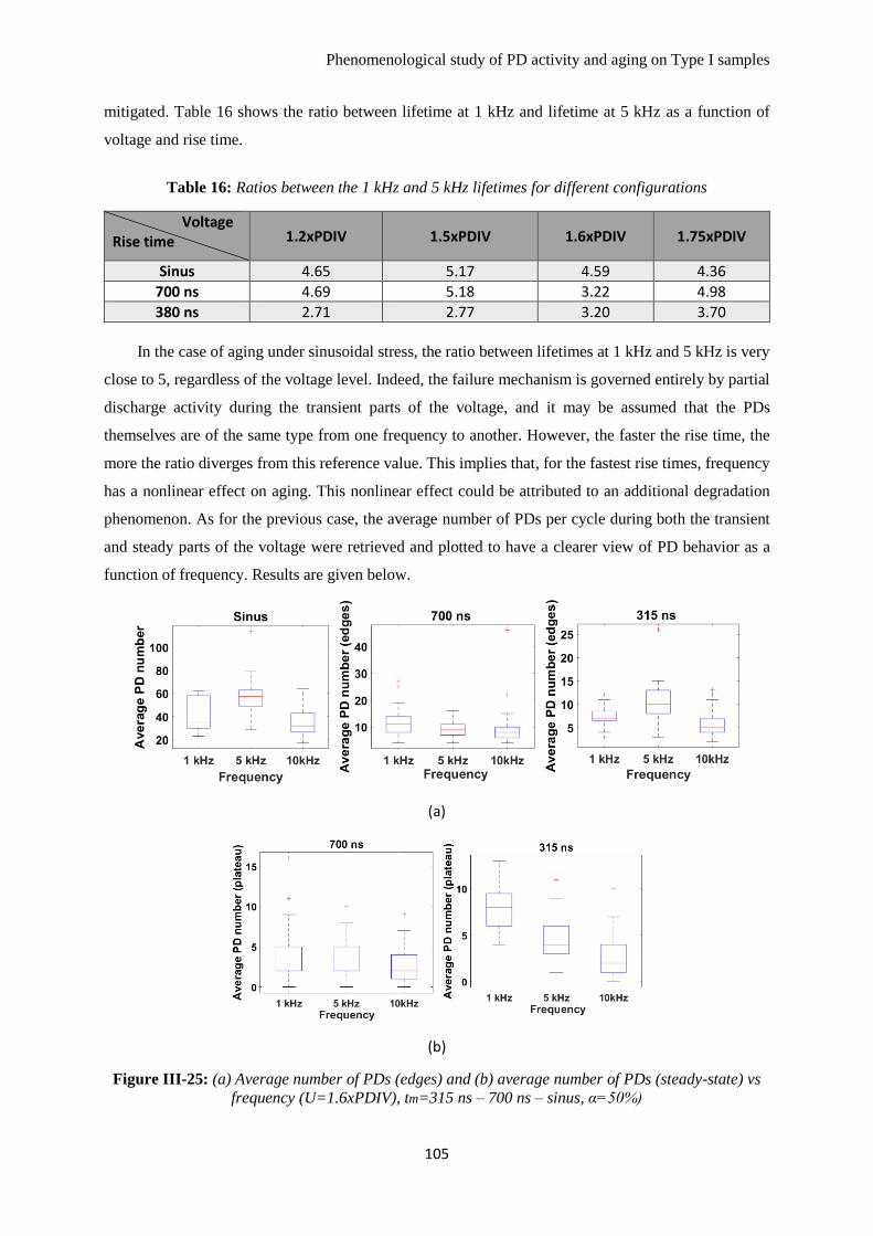
Phenomenological study of PD activity and aging on Type I samples
105
mitigated. Table 16 shows the ratio between lifetime at 1 kHz and lifetime at 5 kHz as a function of
voltage and rise time.
Table 16: Ratios between the 1 kHz and 5 kHz lifetimes for different configurations
Voltage Rise time 1.2xPDIV 1.5xPDIV 1.6xPDIV 1.75xPDIV
Sinus 4.65 5.17 4.59 4.36
700 ns 4.69 5.18 3.22 4.98
380 ns 2.71 2.77 3.20 3.70
In the case of aging under sinusoidal stress, the ratio between lifetimes at 1 kHz and 5 kHz is very
close to 5, regardless of the voltage level. Indeed, the failure mechanism is governed entirely by partial
discharge activity during the transient parts of the voltage, and it may be assumed that the PDs
themselves are of the same type from one frequency to another. However, the faster the rise time, the
more the ratio diverges from this reference value. This implies that, for the fastest rise times, frequency
has a nonlinear effect on aging. This nonlinear effect could be attributed to an additional degradation
phenomenon. As for the previous case, the average number of PDs per cycle during both the transient
and steady parts of the voltage were retrieved and plotted to have a clearer view of PD behavior as a
function of frequency. Results are given below.
(a)
(b)
Figure III-25: (a) Average number of PDs (edges) and (b) average number of PDs (steady-state) vs
frequency (U=1.6xPDIV), tm=315 ns – 700 ns – sinus, α=50%)
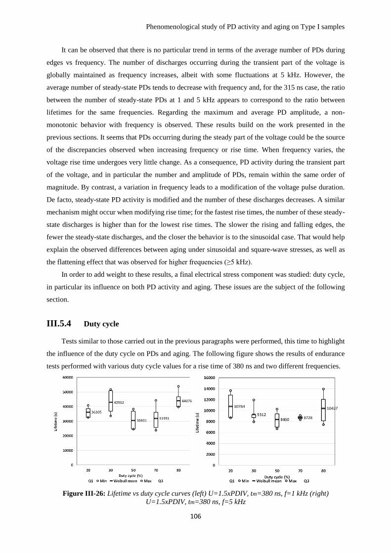
Phenomenological study of PD activity and aging on Type I samples
106
It can be observed that there is no particular trend in terms of the average number of PDs during
edges vs frequency. The number of discharges occurring during the transient part of the voltage is
globally maintained as frequency increases, albeit with some fluctuations at 5 kHz. However, the
average number of steady-state PDs tends to decrease with frequency and, for the 315 ns case, the ratio
between the number of steady-state PDs at 1 and 5 kHz appears to correspond to the ratio between
lifetimes for the same frequencies. Regarding the maximum and average PD amplitude, a non-
monotonic behavior with frequency is observed. These results build on the work presented in the
previous sections. It seems that PDs occurring during the steady part of the voltage could be the source
of the discrepancies observed when increasing frequency or rise time. When frequency varies, the
voltage rise time undergoes very little change. As a consequence, PD activity during the transient part
of the voltage, and in particular the number and amplitude of PDs, remain within the same order of
magnitude. By contrast, a variation in frequency leads to a modification of the voltage pulse duration.
De facto, steady-state PD activity is modified and the number of these discharges decreases. A similar
mechanism might occur when modifying rise time; for the fastest rise times, the number of these steady-
state discharges is higher than for the lowest rise times. The slower the rising and falling edges, the
fewer the steady-state discharges, and the closer the behavior is to the sinusoidal case. That would help
explain the observed differences between aging under sinusoidal and square-wave stresses, as well as
the flattening effect that was observed for higher frequencies (≥5 kHz).
In order to add weight to these results, a final electrical stress component was studied: duty cycle,
in particular its influence on both PD activity and aging. These issues are the subject of the following
section.
III.5.4 Duty cycle
Tests similar to those carried out in the previous paragraphs were performed, this time to highlight
the influence of the duty cycle on PDs and aging. The following figure shows the results of endurance
tests performed with various duty cycle values for a rise time of 380 ns and two different frequencies.
Figure III-26: Lifetime vs duty cycle curves (left) U=1.5xPDIV, tm=380 ns, f=1 kHz (right)
U=1.5xPDIV, tm=380 ns, f=5 kHz
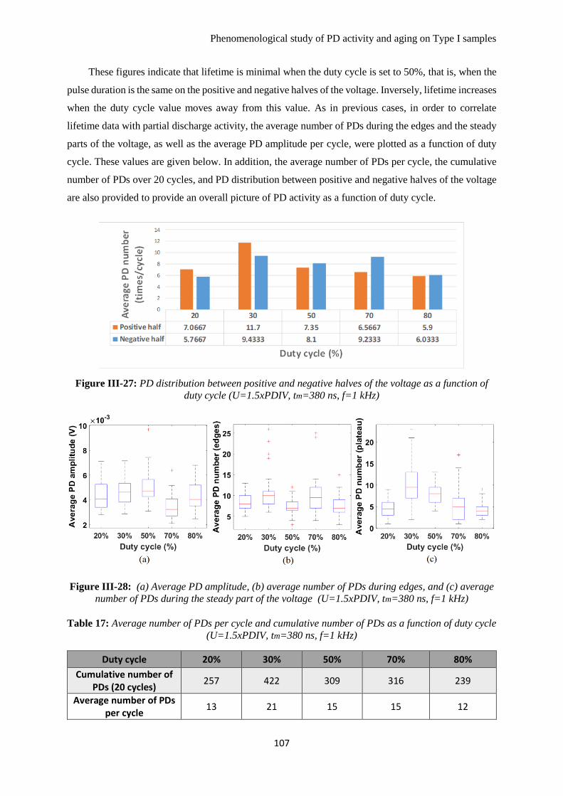
Phenomenological study of PD activity and aging on Type I samples
107
These figures indicate that lifetime is minimal when the duty cycle is set to 50%, that is, when the
pulse duration is the same on the positive and negative halves of the voltage. Inversely, lifetime increases
when the duty cycle value moves away from this value. As in previous cases, in order to correlate
lifetime data with partial discharge activity, the average number of PDs during the edges and the steady
parts of the voltage, as well as the average PD amplitude per cycle, were plotted as a function of duty
cycle. These values are given below. In addition, the average number of PDs per cycle, the cumulative
number of PDs over 20 cycles, and PD distribution between positive and negative halves of the voltage
are also provided to provide an overall picture of PD activity as a function of duty cycle.
Figure III-27: PD distribution between positive and negative halves of the voltage as a function of
duty cycle (U=1.5xPDIV, tm=380 ns, f=1 kHz)
Figure III-28: (a) Average PD amplitude, (b) average number of PDs during edges, and (c) average
number of PDs during the steady part of the voltage (U=1.5xPDIV, tm=380 ns, f=1 kHz)
Table 17: Average number of PDs per cycle and cumulative number of PDs as a function of duty cycle
(U=1.5xPDIV, tm=380 ns, f=1 kHz)
Duty cycle 20% 30% 50% 70% 80%
Cumulative number of PDs (20 cycles)
257 422 309 316 239
Average number of PDs per cycle
13 21 15 15 12
Phenomenological study of PD activity and aging on Type I samples
108
Table 17 shows that the number of PDs varies significantly with duty cycle. The average number
of PDs per cycle is lower when the duty cycle moves away from the 50% level, that is, when the
asymmetry between the positive and negative parts of the voltage is most pronounced. It is even more
obvious considering the cumulative number of PDs over 20 cycles. At the same time, it can be seen in
Figure III-27 that PD distribution between positive and negative halves of the voltage is also affected.
It is worth noting that, for the tests realized with a duty cycle value of 50%, the difference throughout
the study between the average number of PDs in the positive and the negative parts of the voltage rarely
exceeded 1. Nonetheless, when the duty cycle moves away from this central value, differences of about
two or three PDs per cycle can be observed between the two parts of the voltage. This may seem
inconsequential, but it could have significant impact over the entire system lifetime. Finally, Figure
III-28 shows that duty cycle fluctuations do not appear to affect the average PD amplitude or the average
number of PDs during the rising and falling edges. This is not particularly surprising, as the edge
characteristics, in particular the dV/dt and rise time, remain unchanged between configurations. By
contrast, the average number of steady-state PDs experiences variations when varying the duty cycle.
This number is at its maximum for a duty cycle value of between 30% and 50%. These results follow in
the footsteps of what was said before: lifetime discrepancies related to changes in frequency, voltage
magnitude, rise time, or duty cycle values could be directly related to the presence or absence of PDs
during the steady part of the voltage, rather than tied to the traditional PDs that can be found during the
edges. In the light of this assumption, aging and PD activity issues were addressed separately for each
constituent of the electrical stress. To conclude on this subject, a general analysis is presented below to
address all points discussed and summarize the results of this chapter.
III.6 General analysis & conclusion
This work primarily allowed us to determine the influence of the different electrical stress
constituents on aging. Then, as a second step, the obtained lifetime data was correlated with associated
PD activity. Generally speaking, the impact of electrical stress on PDs and aging is consistent with
information found in literature. However, new phenomena were also observed and an innovative
approach was taken in efforts to analyze the mechanisms responsible.
Studying the influence of voltage and overvoltage magnitude showed that, although the presence
of overvoltages increases the number and amplitude of PDs, and thus PD activity in general to a
significant extent, the steady-state voltage magnitude and in particular its level compared to the PDIV
may have an even greater impact on the lifetime of Type I samples due to the possible presence of partial
discharges during the steady part of the voltage. To further illustrate the impact of voltage magnitude,
Figure III-29 shows the cumulative PRPD patterns obtained for different voltage values and
corresponding to different rise time values. The color code reflects the PD density depending on the
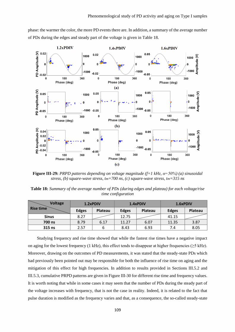
Phenomenological study of PD activity and aging on Type I samples
109
phase: the warmer the color, the more PD events there are. In addition, a summary of the average number
of PDs during the edges and steady part of the voltage is given in Table 18.
Figure III-29: PRPD patterns depending on voltage magnitude (f=1 kHz, α=50%) (a) sinusoidal
stress, (b) square-wave stress, tm=700 ns, (c) square-wave stress, tm=315 ns
Table 18: Summary of the average number of PDs (during edges and plateau) for each voltage/rise
time configuration
Voltage Rise time
1.2xPDIV 1.4xPDIV 1.6xPDIV
Edges Plateau Edges Plateau Edges Plateau
Sinus 8.27 12.75 41.15
700 ns 8.79 6.17 11.27 6.07 11.35 3.87
315 ns 2.57 6 8.43 6.93 7.4 8.05
Studying frequency and rise time showed that while the fastest rise times have a negative impact
on aging for the lowest frequency (1 kHz), this effect tends to disappear at higher frequencies (≥5 kHz).
Moreover, drawing on the outcomes of PD measurements, it was stated that the steady-state PDs which
had previously been pointed out may be responsible for both the influence of rise time on aging and the
mitigation of this effect for high frequencies. In addition to results provided in Sections III.5.2 and
III.5.3, cumulative PRPD patterns are given in Figure III-30 for different rise time and frequency values.
It is worth noting that while in some cases it may seem that the number of PDs during the steady part of
the voltage increases with frequency, that is not the case in reality. Indeed, it is related to the fact that
pulse duration is modified as the frequency varies and that, as a consequence, the so-called steady-state
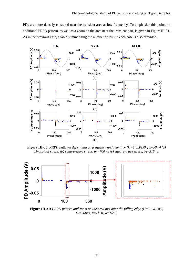
Phenomenological study of PD activity and aging on Type I samples
110
PDs are more densely clustered near the transient area at low frequency. To emphasize this point, an
additional PRPD pattern, as well as a zoom on the area near the transient part, is given in Figure III-31.
As in the previous case, a table summarizing the number of PDs in each case is also provided.
Figure III-30: PRPD patterns depending on frequency and rise time (U=1.6xPDIV, α=50%) (a)
sinusoidal stress, (b) square-wave stress, tm=700 ns (c) square-wave stress, tm=315 ns
Figure III-31: PRPD pattern and zoom on the area just after the falling edge (U=1.6xPDIV,
tm=700ns, f=5 kHz, α=50%)
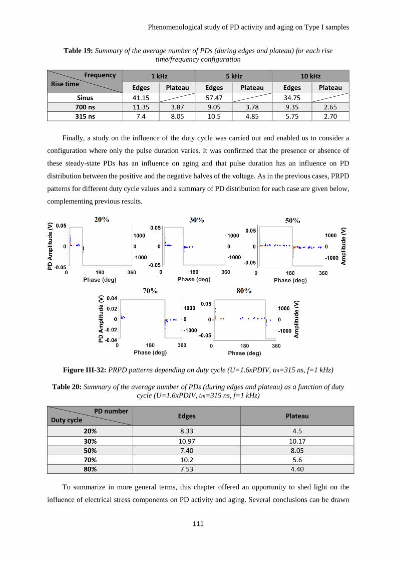
Phenomenological study of PD activity and aging on Type I samples
111
Table 19: Summary of the average number of PDs (during edges and plateau) for each rise
time/frequency configuration
Frequency Rise time
1 kHz 5 kHz 10 kHz
Edges Plateau Edges Plateau Edges Plateau
Sinus 41.15 57.47 34.75
700 ns 11.35 3.87 9.05 3.78 9.35 2.65
315 ns 7.4 8.05 10.5 4.85 5.75 2.70
Finally, a study on the influence of the duty cycle was carried out and enabled us to consider a
configuration where only the pulse duration varies. It was confirmed that the presence or absence of
these steady-state PDs has an influence on aging and that pulse duration has an influence on PD
distribution between the positive and the negative halves of the voltage. As in the previous cases, PRPD
patterns for different duty cycle values and a summary of PD distribution for each case are given below,
complementing previous results.
Figure III-32: PRPD patterns depending on duty cycle (U=1.6xPDIV, tm=315 ns, f=1 kHz)
Table 20: Summary of the average number of PDs (during edges and plateau) as a function of duty
cycle (U=1.6xPDIV, tm=315 ns, f=1 kHz)
PD number Duty cycle
Edges Plateau
20% 8.33 4.5
30% 10.97 10.17
50% 7.40 8.05
70% 10.2 5.6
80% 7.53 4.40
To summarize in more general terms, this chapter offered an opportunity to shed light on the
influence of electrical stress components on PD activity and aging. Several conclusions can be drawn
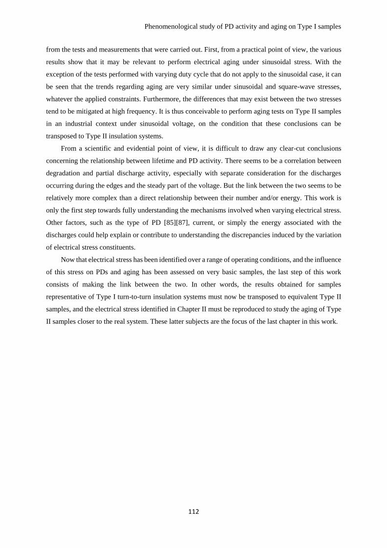
Phenomenological study of PD activity and aging on Type I samples
112
from the tests and measurements that were carried out. First, from a practical point of view, the various
results show that it may be relevant to perform electrical aging under sinusoidal stress. With the
exception of the tests performed with varying duty cycle that do not apply to the sinusoidal case, it can
be seen that the trends regarding aging are very similar under sinusoidal and square-wave stresses,
whatever the applied constraints. Furthermore, the differences that may exist between the two stresses
tend to be mitigated at high frequency. It is thus conceivable to perform aging tests on Type II samples
in an industrial context under sinusoidal voltage, on the condition that these conclusions can be
transposed to Type II insulation systems.
From a scientific and evidential point of view, it is difficult to draw any clear-cut conclusions
concerning the relationship between lifetime and PD activity. There seems to be a correlation between
degradation and partial discharge activity, especially with separate consideration for the discharges
occurring during the edges and the steady part of the voltage. But the link between the two seems to be
relatively more complex than a direct relationship between their number and/or energy. This work is
only the first step towards fully understanding the mechanisms involved when varying electrical stress.
Other factors, such as the type of PD [85][87], current, or simply the energy associated with the
discharges could help explain or contribute to understanding the discrepancies induced by the variation
of electrical stress constituents.
Now that electrical stress has been identified over a range of operating conditions, and the influence
of this stress on PDs and aging has been assessed on very basic samples, the last step of this work
consists of making the link between the two. In other words, the results obtained for samples
representative of Type I turn-to-turn insulation systems must now be transposed to equivalent Type II
samples, and the electrical stress identified in Chapter II must be reproduced to study the aging of Type
II samples closer to the real system. These latter subjects are the focus of the last chapter in this work.

Investigations into aging and underlying phenomena in Type II machines
114
Chapter IV. Investigations into aging and underlying
phenomena in Type II machines
IV.1 Brief introduction
After a brief examination of the state of the art, research reported in previous sections enabled us
to identify the electrical stress in a Type II machine as a function of various electrical and geometrical
parameters, and to assess the influence of this electrical stress on aging and partial discharge activity
considering very basic samples representative of Type I turn-to-turn insulation systems. However, it is
necessary to go further to address both the causes and effects of the existence of PDs in a Type II
electromechanical chain using SiC-based components. With this goal in mind, the purpose of this last
chapter is now to assess the influence of electrical stress on samples that are representative of the actual
system itself to bridge the gap between phenomenological study and stress identification and, at the
same time, between Type I and Type II.
This chapter is divided into two parts: the first part is devoted to the translation from Type I turn-
to-turn insulation systems to Type II equivalent insulation systems that are actually used in high voltage
machines. The second part focuses on extending of the study of PD activity and aging to Type II phase-
to-phase and phase-to-ground insulation systems. As it was explained in Chapter II, these insulation
systems are indeed more likely to be subject to partial discharges. This chapter is the last building block
of the full study, offering complete consistency of information related to the study of PDs and aging in
an electromechanical chain in the presence of constraints related to SiC, in the context of Type II
machines.
IV.2 Transition from Type I to Type II conductor pairs
IV.2.1 Purpose of the study
In the previous chapter, a study on the influence of the different electrical stress constituents on
PDs and aging was performed on twisted pairs of enameled wires, representative of Type I turn-to-turn
insulation systems. The purpose of this section is now to determine whether or not the conclusions
emerging from that study can be transposed to Type II insulation systems, which are more complex
because they are composed of different types of organic and inorganic insulating materials. A reduced
test plan, compared to that of Chapter III, was therefore set up to check whether the main trends are the
same.
The details of the experimental setup, test plan, as well as the main results of this study are given
below following the same structure as that used in Chapter III.
Investigations into aging and underlying phenomena in Type II machines
115
IV.2.2 Experimental setup & test plan
IV.2.2.1 Investigation on sample characteristics
As specified in Section II.3.1, Type II high voltage machines generally present formed wound coils
constituted of flat wires stacked on top of each other. In general, the turn-to-turn insulation of such
machines consists of a polyimide film coating, sometimes reinforced with Teflon-FEP, as is the case
here. The samples used for this study are therefore representative of this type of insulation system. They
comprise pairs of insulated conductors that are held together, with the terminals splayed apart and
processed according to production standards. The insulated conductors are in contact along the length
of the straight portion to simulate the contact between turns in a coil. The contact between those
conductors is maintained by a wrapping that provides the pressing function [15]. Pictures of the samples
are provided below.
Figure IV-1: Type II pairs of insulated conductors
Two types of insulated conductor pairs were considered in the study. The first type, which is
referred to as “Type O”, is representative of the materials that are actually used for the turn-to-turn
insulation of machines. The second type, which is referred to as “Type A”, is an improved version (in
terms of electrical insulation) of the “Type O” sample. The insulating materials remain unchanged
between the two. The only difference resides in the thickness of the covering material, i.e. the polyimide
film coating.
Investigations into the electrical characteristics of the samples were carried out in order to assess
their tolerance towards PDs and also to determine the levels of stress to apply during aging. PDIV
measurements and breakdown tests were thus performed following the same procedure as that applied
in III.2.3. The results are given in Table 21 for both types of pairs of conductors. In parallel, simulations
were carried out to estimate this same PDIV and compare the value to experimental results, as well as
Investigations into aging and underlying phenomena in Type II machines
116
to obtain a view of the electric field lines and potential distribution in the area of the two conductors. A
simulation tool developed by IRT Saint Exupéry called AIRLIFT – pArtial dIscharge Risk evaLuatIon
soFTware - was used to run these simulations. To summarize, this simulation tool uses a 2D model
based on the current state of discharge physics in homogenous fields (Townsend’s theory) derived for
inhomogeneous fields to model partial discharge inception voltage in a numerical way. The results are
also given below.
Table 21: PDIVs for both types of samples (Type O and Type A)
Sample number Type O Type A
PDIV (kVpk) Breakdown
voltage (kVpk) PDIV (kVpk)
Breakdown voltage (kVpk)
1 1.44 8.68 2.029 13.22
2 1.353 10.21 2.305 14.32
3 1.62 9.78 2.41 15.34
4 1.528 10.18 2.411 15.26
5 1.442 10.18 2.101 14.83
Average 1.4766 9.806 2.2512 14.594
Simulation 1.410 2.590
Figure IV-2: (a) Electric field distribution (V/m) and (b) PDIV distribution (V) in the area of a Type
O sample
The PDIV values obtained experimentally and numerically are quite similar to each other. This is
especially true in the case of Type O samples, for which the proposed simulation method is highly
representative of reality and able to identify the most likely area for PD inception. Regarding Type A
samples, the gap between experimental and numerical values is slightly larger. This gap, as well as the
PDIV difference between the two types of samples, can be explained by the difference between the
percentage overlap of the tape in both cases. In the cases of Type O samples, the percentage overlap of
the tape is such that the total insulation thickness is a multiple of tape thickness throughout the length
of the conductors. As the geometry is independent of the length, it is thus convenient to use a 2D model
to estimate PDIV values. By contrast, the percentage overlap is higher for Type A samples, such that
the insulation thickness is not the same throughout the length of the conductors (Figure IV-3 illustrates
Investigations into aging and underlying phenomena in Type II machines
117
this point). As a consequence, there are areas where insulation thickness is the same as for Type O
samples, and areas where the insulation is thicker. This explains why the PDIV is higher for Type A
samples, as well as why the gap between experimental and numerical values is larger in the latter case:
the 2D model does not take full account of the thickness inhomogeneity throughout the length.
Simulation was thus carried out considering an average value for insulation thickness.
Figure IV-3: Illustration of the different types of overlap used for Type II machine insulation
Based on these results, preliminary conclusions can be drawn regarding the existence of partial
discharges in turn-to-turn insulation systems. Given the average PDIV values (respectively 1477 and
2251 Vpeak for Type O and Type A conductor pairs), and considering the results of the stress
identification performed in Chapter II, it is confirmed that there is little chance of PD inception occurring
in the insulation between turns. It is still important to note that, compared with a real machine, the PDIV
of back-to-back specimens can be higher as the impregnation is nearly perfect (the straight part is not
put in a metallic enclosure). The maximum turn-to-turn voltage was found to be a few hundred volts for
the fastest inverters, so the insulation system structure prevents the appearance of any PD events. This
holds all the more true as the insulation of the considered samples is representative of machines that are
supposed to operate with the lowest DC bus voltage in the range. For the highest DC bus voltages, it
may be assumed that the insulation is all the more reinforced, whereas the maximum turn-to-turn stresses
may not necessarily be much more stressful than in the case of the lowest DC bus voltages. To be more
specific regarding this last point, and referring back to the results given in Section II.5, it can be seen
that the worst case in terms of maximum relative turn-to-turn stresses is encountered for inverters C and
E (respectively 45.71% and 15.6% of the DC bus voltage, and a few hundred volts in absolute terms).
Those inverters are both supposed to operate at the lowest DC bus voltage. For the highest DC bus
voltages, however, the worst case is encountered with inverter B (8.86% of the DC bus voltage). An
extrapolation of this result for the nominal voltage value leads to a maximal absolute turn-to-turn value
that also does not exceed a few hundred volts, despite the voltage increase. Therefore, given the fact that
the maximal absolute turn-to-turn values are quite similar in both cases, there are potentially far fewer
chances to incept PDs between turns in a machine operating for the highest DC bus voltages and thus
equipped with a reinforced electrical insulation system.
Investigations into aging and underlying phenomena in Type II machines
118
As a consequence of the fact that the turn-to-turn insulation does not represent the weakest point
in the machine, that aspect was not the main focus of the study. The number of tests and, in turn, the test
plan were reduced drastically, and the purpose of the following part is mainly to assess whether the
results obtained in the previous chapter can be transposed to Type II insulation systems.
Due to the nature of the samples representative of Type II turn-to-turn insulation systems, which
are somewhat different from the basic Type I twisted pairs of enameled wires that were studied
previously, the experimental setups used for this part of the study are different from those presented in
Section III.2. Experiments were carried out at two different locations, with the tests under sinusoidal
stress at one site, and the tests under square-wave stress at the other.
IV.2.2.2 Aging under sinusoidal stress
Endurance tests under sinusoidal stress were performed using the same voltage supply to be used
for aging the motorettes representative of Type II phase-to-ground and phase-to-phase voltages. This
voltage source was specially designed for aging very capacitive samples based on their characteristics
and the results obtained during the previous study. This scaling is the subject of particular attention in
Section IV.3.2. However, at this point, it can be stated that this voltage source can deliver a sinusoidal
voltage up to 10 kV peak, with a frequency ranging from 1 to 10 kHz. This voltage supply is comprised
of six independent amplifiers, each coupled with a main transformer. This makes it possible to supply
six channels independently. A schematic layout of the voltage source is given below.
Figure IV-4: Schematic layout of the experimental bench used for aging under sinusoidal stress
As with the experimental setup in Chapter III, lifetime is estimated on each channel independently
using the current limitation of the voltage supply. Voltage is controlled both using a high voltage probe
(Testec TT-SI 9010) and via a measurement taken directly on the voltage source. Finally, PD
measurements are also achieved according to the same model as that in Chapter III, except that the 20
acquisitions are repeated every hour instead of only during three different aging stages. Finally, the data
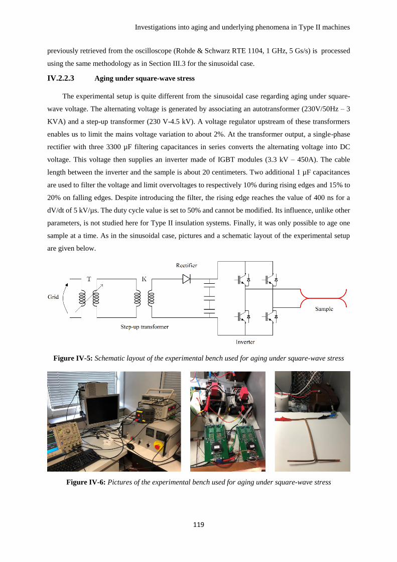
Investigations into aging and underlying phenomena in Type II machines
119
previously retrieved from the oscilloscope (Rohde & Schwarz RTE 1104, 1 GHz, 5 Gs/s) is processed
using the same methodology as in Section III.3 for the sinusoidal case.
IV.2.2.3 Aging under square-wave stress
The experimental setup is quite different from the sinusoidal case regarding aging under square-
wave voltage. The alternating voltage is generated by associating an autotransformer (230V/50Hz – 3
KVA) and a step-up transformer (230 V-4.5 kV). A voltage regulator upstream of these transformers
enables us to limit the mains voltage variation to about 2%. At the transformer output, a single-phase
rectifier with three 3300 µF filtering capacitances in series converts the alternating voltage into DC
voltage. This voltage then supplies an inverter made of IGBT modules (3.3 kV – 450A). The cable
length between the inverter and the sample is about 20 centimeters. Two additional 1 µF capacitances
are used to filter the voltage and limit overvoltages to respectively 10% during rising edges and 15% to
20% on falling edges. Despite introducing the filter, the rising edge reaches the value of 400 ns for a
dV/dt of 5 kV/µs. The duty cycle value is set to 50% and cannot be modified. Its influence, unlike other
parameters, is not studied here for Type II insulation systems. Finally, it was only possible to age one
sample at a time. As in the sinusoidal case, pictures and a schematic layout of the experimental setup
are given below.
Figure IV-5: Schematic layout of the experimental bench used for aging under square-wave stress
Figure IV-6: Pictures of the experimental bench used for aging under square-wave stress
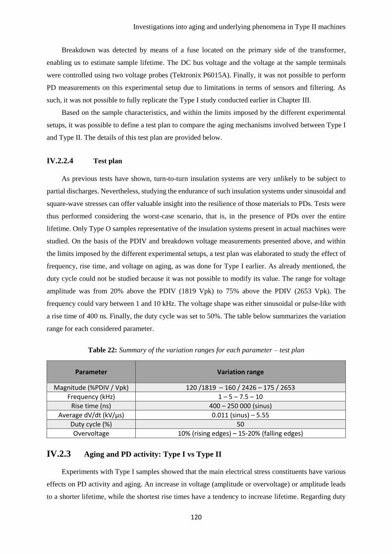
Investigations into aging and underlying phenomena in Type II machines
120
Breakdown was detected by means of a fuse located on the primary side of the transformer,
enabling us to estimate sample lifetime. The DC bus voltage and the voltage at the sample terminals
were controlled using two voltage probes (Tektronix P6015A). Finally, it was not possible to perform
PD measurements on this experimental setup due to limitations in terms of sensors and filtering. As
such, it was not possible to fully replicate the Type I study conducted earlier in Chapter III.
Based on the sample characteristics, and within the limits imposed by the different experimental
setups, it was possible to define a test plan to compare the aging mechanisms involved between Type I
and Type II. The details of this test plan are provided below.
IV.2.2.4 Test plan
As previous tests have shown, turn-to-turn insulation systems are very unlikely to be subject to
partial discharges. Nevertheless, studying the endurance of such insulation systems under sinusoidal and
square-wave stresses can offer valuable insight into the resilience of those materials to PDs. Tests were
thus performed considering the worst-case scenario, that is, in the presence of PDs over the entire
lifetime. Only Type O samples representative of the insulation systems present in actual machines were
studied. On the basis of the PDIV and breakdown voltage measurements presented above, and within
the limits imposed by the different experimental setups, a test plan was elaborated to study the effect of
frequency, rise time, and voltage on aging, as was done for Type I earlier. As already mentioned, the
duty cycle could not be studied because it was not possible to modify its value. The range for voltage
amplitude was from 20% above the PDIV (1819 Vpk) to 75% above the PDIV (2653 Vpk). The
frequency could vary between 1 and 10 kHz. The voltage shape was either sinusoidal or pulse-like with
a rise time of 400 ns. Finally, the duty cycle was set to 50%. The table below summarizes the variation
range for each considered parameter.
Table 22: Summary of the variation ranges for each parameter – test plan
Parameter Variation range
Magnitude (%PDIV / Vpk) 120 /1819 – 160 / 2426 – 175 / 2653
Frequency (kHz) 1 – 5 – 7.5 – 10
Rise time (ns) 400 – 250 000 (sinus)
Average dV/dt (kV/µs) 0.011 (sinus) – 5.55
Duty cycle (%) 50
Overvoltage 10% (rising edges) – 15-20% (falling edges)
IV.2.3 Aging and PD activity: Type I vs Type II
Experiments with Type I samples showed that the main electrical stress constituents have various
effects on PD activity and aging. An increase in voltage (amplitude or overvoltage) or amplitude leads
to a shorter lifetime, while the shortest rise times have a tendency to increase lifetime. Regarding duty
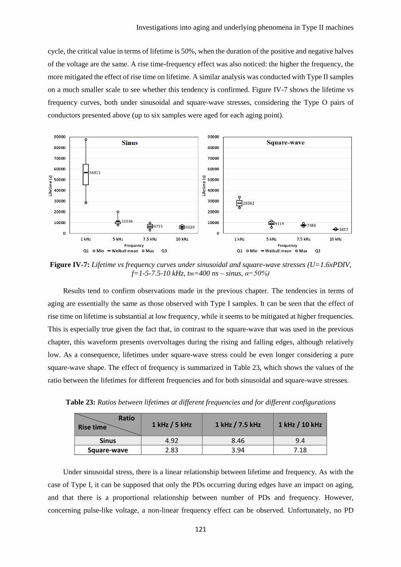
Investigations into aging and underlying phenomena in Type II machines
121
cycle, the critical value in terms of lifetime is 50%, when the duration of the positive and negative halves
of the voltage are the same. A rise time-frequency effect was also noticed: the higher the frequency, the
more mitigated the effect of rise time on lifetime. A similar analysis was conducted with Type II samples
on a much smaller scale to see whether this tendency is confirmed. Figure IV-7 shows the lifetime vs
frequency curves, both under sinusoidal and square-wave stresses, considering the Type O pairs of
conductors presented above (up to six samples were aged for each aging point).
Figure IV-7: Lifetime vs frequency curves under sinusoidal and square-wave stresses (U=1.6xPDIV,
f=1-5-7.5-10 kHz, tm=400 ns – sinus, α=50%)
Results tend to confirm observations made in the previous chapter. The tendencies in terms of
aging are essentially the same as those observed with Type I samples. It can be seen that the effect of
rise time on lifetime is substantial at low frequency, while it seems to be mitigated at higher frequencies.
This is especially true given the fact that, in contrast to the square-wave that was used in the previous
chapter, this waveform presents overvoltages during the rising and falling edges, although relatively
low. As a consequence, lifetimes under square-wave stress could be even longer considering a pure
square-wave shape. The effect of frequency is summarized in Table 23, which shows the values of the
ratio between the lifetimes for different frequencies and for both sinusoidal and square-wave stresses.
Table 23: Ratios between lifetimes at different frequencies and for different configurations
Ratio Rise time 1 kHz / 5 kHz 1 kHz / 7.5 kHz 1 kHz / 10 kHz
Sinus 4.92 8.46 9.4
Square-wave 2.83 3.94 7.18
Under sinusoidal stress, there is a linear relationship between lifetime and frequency. As with the
case of Type I, it can be supposed that only the PDs occurring during edges have an impact on aging,
and that there is a proportional relationship between number of PDs and frequency. However,
concerning pulse-like voltage, a non-linear frequency effect can be observed. Unfortunately, no PD
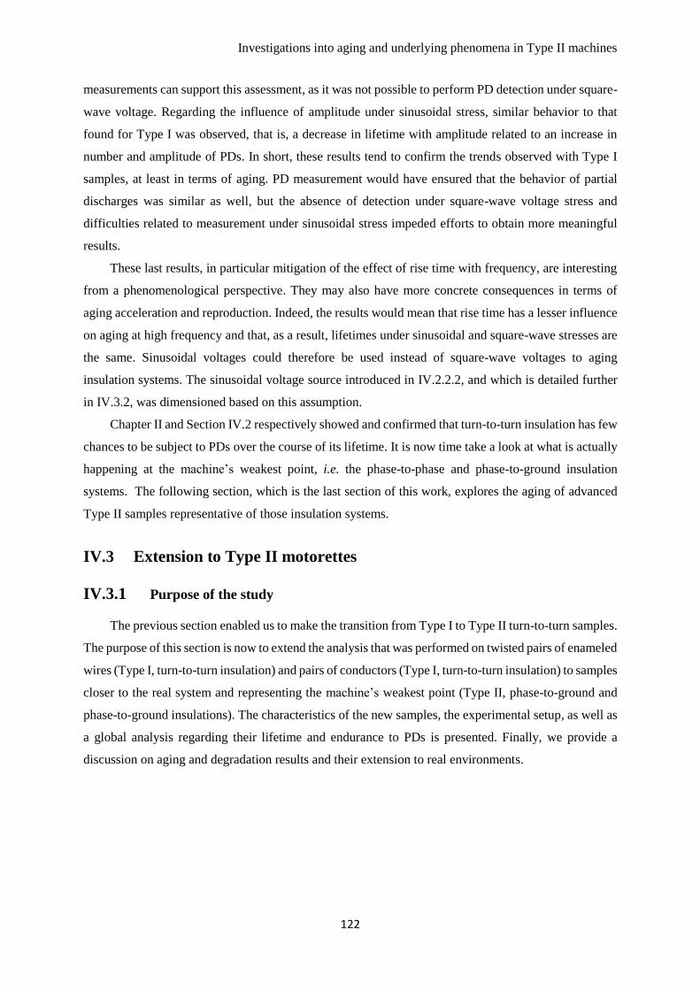
Investigations into aging and underlying phenomena in Type II machines
122
measurements can support this assessment, as it was not possible to perform PD detection under square-
wave voltage. Regarding the influence of amplitude under sinusoidal stress, similar behavior to that
found for Type I was observed, that is, a decrease in lifetime with amplitude related to an increase in
number and amplitude of PDs. In short, these results tend to confirm the trends observed with Type I
samples, at least in terms of aging. PD measurement would have ensured that the behavior of partial
discharges was similar as well, but the absence of detection under square-wave voltage stress and
difficulties related to measurement under sinusoidal stress impeded efforts to obtain more meaningful
results.
These last results, in particular mitigation of the effect of rise time with frequency, are interesting
from a phenomenological perspective. They may also have more concrete consequences in terms of
aging acceleration and reproduction. Indeed, the results would mean that rise time has a lesser influence
on aging at high frequency and that, as a result, lifetimes under sinusoidal and square-wave stresses are
the same. Sinusoidal voltages could therefore be used instead of square-wave voltages to aging
insulation systems. The sinusoidal voltage source introduced in IV.2.2.2, and which is detailed further
in IV.3.2, was dimensioned based on this assumption.
Chapter II and Section IV.2 respectively showed and confirmed that turn-to-turn insulation has few
chances to be subject to PDs over the course of its lifetime. It is now time take a look at what is actually
happening at the machine’s weakest point, i.e. the phase-to-phase and phase-to-ground insulation
systems. The following section, which is the last section of this work, explores the aging of advanced
Type II samples representative of those insulation systems.
IV.3 Extension to Type II motorettes
IV.3.1 Purpose of the study
The previous section enabled us to make the transition from Type I to Type II turn-to-turn samples.
The purpose of this section is now to extend the analysis that was performed on twisted pairs of enameled
wires (Type I, turn-to-turn insulation) and pairs of conductors (Type I, turn-to-turn insulation) to samples
closer to the real system and representing the machine’s weakest point (Type II, phase-to-ground and
phase-to-ground insulations). The characteristics of the new samples, the experimental setup, as well as
a global analysis regarding their lifetime and endurance to PDs is presented. Finally, we provide a
discussion on aging and degradation results and their extension to real environments.
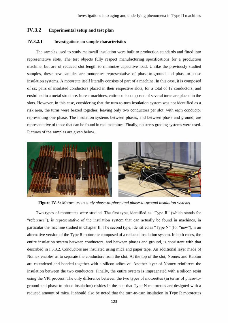
Investigations into aging and underlying phenomena in Type II machines
123
IV.3.2 Experimental setup and test plan
IV.3.2.1 Investigations on sample characteristics
The samples used to study mainwall insulation were built to production standards and fitted into
representative slots. The test objects fully respect manufacturing specifications for a production
machine, but are of reduced slot length to minimize capacitive load. Unlike the previously studied
samples, these new samples are motorettes representative of phase-to-ground and phase-to-phase
insulation systems. A motorette itself literally consists of part of a machine. In this case, it is composed
of six pairs of insulated conductors placed in their respective slots, for a total of 12 conductors, and
enshrined in a metal structure. In real machines, entire coils composed of several turns are placed in the
slots. However, in this case, considering that the turn-to-turn insulation system was not identified as a
risk area, the turns were brazed together, leaving only two conductors per slot, with each conductor
representing one phase. The insulation systems between phases, and between phase and ground, are
representative of those that can be found in real machines. Finally, no stress grading systems were used.
Pictures of the samples are given below.
Figure IV-8: Motorettes to study phase-to-phase and phase-to-ground insulation systems
Two types of motorettes were studied. The first type, identified as “Type R” (which stands for
“reference”), is representative of the insulation system that can actually be found in machines, in
particular the machine studied in Chapter II. The second type, identified as “Type N” (for “new”), is an
alternative version of the Type R motorette composed of a reduced insulation system. In both cases, the
entire insulation system between conductors, and between phases and ground, is consistent with that
described in I.3.3.2. Conductors are insulated using mica and paper tape. An additional layer made of
Nomex enables us to separate the conductors from the slot. At the top of the slot, Nomex and Kapton
are calendered and bonded together with a silicon adhesive. Another layer of Nomex reinforces the
insulation between the two conductors. Finally, the entire system is impregnated with a silicon resin
using the VPI process. The only difference between the two types of motorettes (in terms of phase-to-
ground and phase-to-phase insulation) resides in the fact that Type N motorettes are designed with a
reduced amount of mica. It should also be noted that the turn-to-turn insulation in Type R motorettes
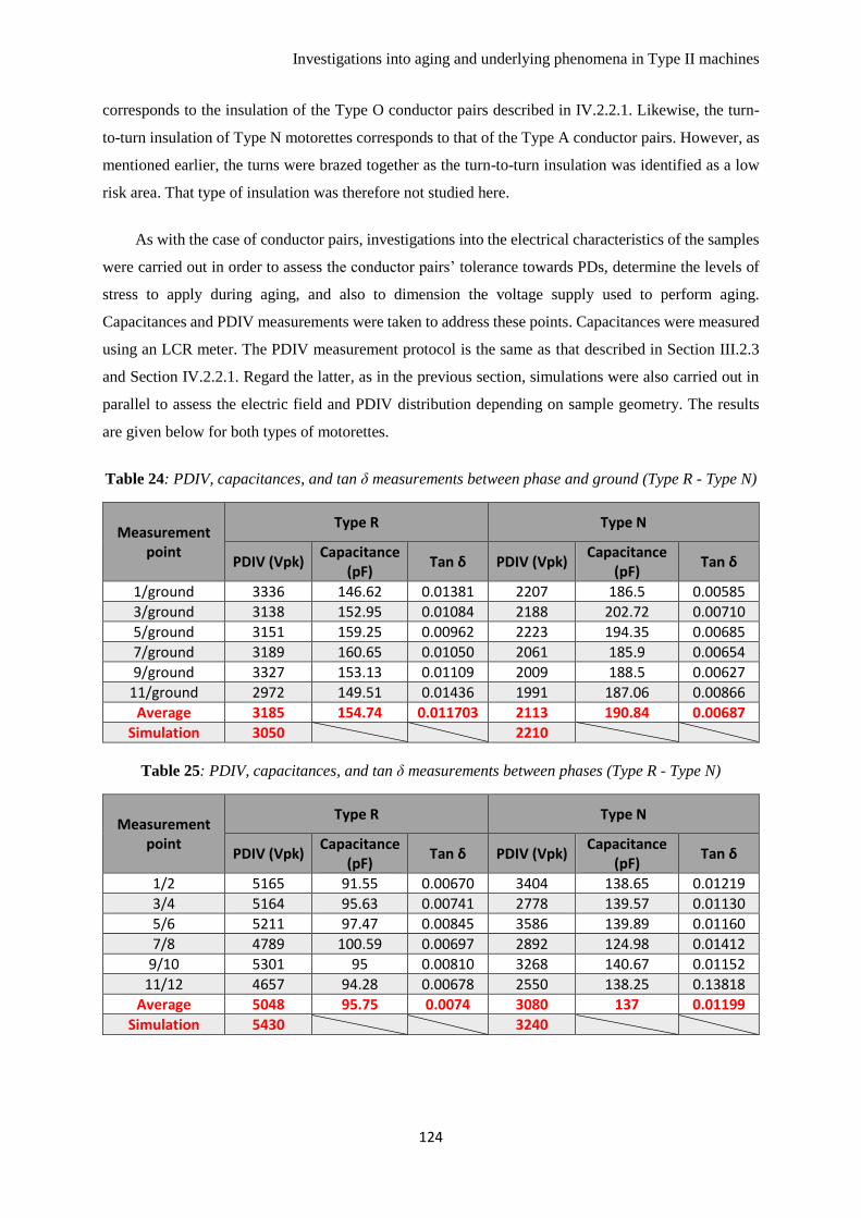
Investigations into aging and underlying phenomena in Type II machines
124
corresponds to the insulation of the Type O conductor pairs described in IV.2.2.1. Likewise, the turn-
to-turn insulation of Type N motorettes corresponds to that of the Type A conductor pairs. However, as
mentioned earlier, the turns were brazed together as the turn-to-turn insulation was identified as a low
risk area. That type of insulation was therefore not studied here.
As with the case of conductor pairs, investigations into the electrical characteristics of the samples
were carried out in order to assess the conductor pairs’ tolerance towards PDs, determine the levels of
stress to apply during aging, and also to dimension the voltage supply used to perform aging.
Capacitances and PDIV measurements were taken to address these points. Capacitances were measured
using an LCR meter. The PDIV measurement protocol is the same as that described in Section III.2.3
and Section IV.2.2.1. Regard the latter, as in the previous section, simulations were also carried out in
parallel to assess the electric field and PDIV distribution depending on sample geometry. The results
are given below for both types of motorettes.
Table 24: PDIV, capacitances, and tan δ measurements between phase and ground (Type R - Type N)
Measurement point
Type R Type N
PDIV (Vpk) Capacitance
(pF) Tan δ PDIV (Vpk)
Capacitance (pF)
Tan δ
1/ground 3336 146.62 0.01381 2207 186.5 0.00585
3/ground 3138 152.95 0.01084 2188 202.72 0.00710
5/ground 3151 159.25 0.00962 2223 194.35 0.00685
7/ground 3189 160.65 0.01050 2061 185.9 0.00654
9/ground 3327 153.13 0.01109 2009 188.5 0.00627
11/ground 2972 149.51 0.01436 1991 187.06 0.00866
Average 3185 154.74 0.011703 2113 190.84 0.00687
Simulation 3050 2210
Table 25: PDIV, capacitances, and tan δ measurements between phases (Type R - Type N)
Measurement point
Type R Type N
PDIV (Vpk) Capacitance
(pF) Tan δ PDIV (Vpk)
Capacitance (pF)
Tan δ
1/2 5165 91.55 0.00670 3404 138.65 0.01219
3/4 5164 95.63 0.00741 2778 139.57 0.01130
5/6 5211 97.47 0.00845 3586 139.89 0.01160
7/8 4789 100.59 0.00697 2892 124.98 0.01412
9/10 5301 95 0.00810 3268 140.67 0.01152
11/12 4657 94.28 0.00678 2550 138.25 0.13818
Average 5048 95.75 0.0074 3080 137 0.01199
Simulation 5430 3240
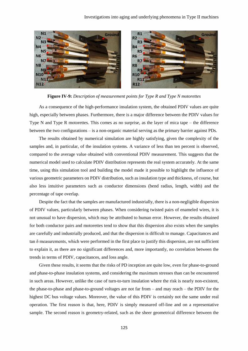
Investigations into aging and underlying phenomena in Type II machines
125
Figure IV-9: Description of measurement points for Type R and Type N motorettes
As a consequence of the high-performance insulation system, the obtained PDIV values are quite
high, especially between phases. Furthermore, there is a major difference between the PDIV values for
Type N and Type R motorettes. This comes as no surprise, as the layer of mica tape – the difference
between the two configurations – is a non-organic material serving as the primary barrier against PDs.
The results obtained by numerical simulation are highly satisfying, given the complexity of the
samples and, in particular, of the insulation systems. A variance of less than ten percent is observed,
compared to the average value obtained with conventional PDIV measurement. This suggests that the
numerical model used to calculate PDIV distribution represents the real system accurately. At the same
time, using this simulation tool and building the model made it possible to highlight the influence of
various geometric parameters on PDIV distribution, such as insulation type and thickness, of course, but
also less intuitive parameters such as conductor dimensions (bend radius, length, width) and the
percentage of tape overlap.
Despite the fact that the samples are manufactured industrially, there is a non-negligible dispersion
of PDIV values, particularly between phases. When considering twisted pairs of enameled wires, it is
not unusual to have dispersion, which may be attributed to human error. However, the results obtained
for both conductor pairs and motorettes tend to show that this dispersion also exists when the samples
are carefully and industrially produced, and that the dispersion is difficult to manage. Capacitances and
tan δ measurements, which were performed in the first place to justify this dispersion, are not sufficient
to explain it, as there are no significant differences and, more importantly, no correlation between the
trends in terms of PDIV, capacitances, and loss angle.
Given these results, it seems that the risks of PD inception are quite low, even for phase-to-ground
and phase-to-phase insulation systems, and considering the maximum stresses than can be encountered
in such areas. However, unlike the case of turn-to-turn insulation where the risk is nearly non-existent,
the phase-to-phase and phase-to-ground voltages are not far from – and may reach – the PDIV for the
highest DC bus voltage values. Moreover, the value of this PDIV is certainly not the same under real
operation. The first reason is that, here, PDIV is simply measured off-line and on a representative
sample. The second reason is geometry-related, such as the sheer geometrical difference between the
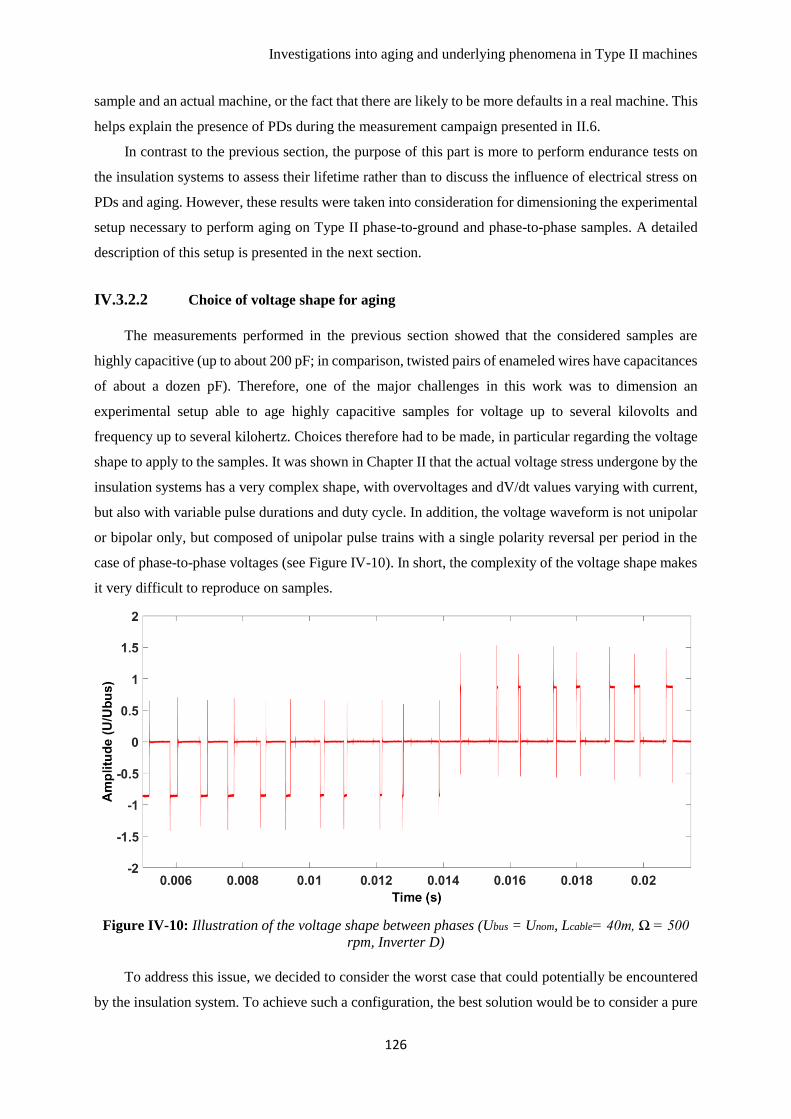
Investigations into aging and underlying phenomena in Type II machines
126
sample and an actual machine, or the fact that there are likely to be more defaults in a real machine. This
helps explain the presence of PDs during the measurement campaign presented in II.6.
In contrast to the previous section, the purpose of this part is more to perform endurance tests on
the insulation systems to assess their lifetime rather than to discuss the influence of electrical stress on
PDs and aging. However, these results were taken into consideration for dimensioning the experimental
setup necessary to perform aging on Type II phase-to-ground and phase-to-phase samples. A detailed
description of this setup is presented in the next section.
IV.3.2.2 Choice of voltage shape for aging
The measurements performed in the previous section showed that the considered samples are
highly capacitive (up to about 200 pF; in comparison, twisted pairs of enameled wires have capacitances
of about a dozen pF). Therefore, one of the major challenges in this work was to dimension an
experimental setup able to age highly capacitive samples for voltage up to several kilovolts and
frequency up to several kilohertz. Choices therefore had to be made, in particular regarding the voltage
shape to apply to the samples. It was shown in Chapter II that the actual voltage stress undergone by the
insulation systems has a very complex shape, with overvoltages and dV/dt values varying with current,
but also with variable pulse durations and duty cycle. In addition, the voltage waveform is not unipolar
or bipolar only, but composed of unipolar pulse trains with a single polarity reversal per period in the
case of phase-to-phase voltages (see Figure IV-10). In short, the complexity of the voltage shape makes
it very difficult to reproduce on samples.
Figure IV-10: Illustration of the voltage shape between phases (Ubus = Unom, Lcable= 40m, Ω = 500
rpm, Inverter D)
To address this issue, we decided to consider the worst case that could potentially be encountered
by the insulation system. To achieve such a configuration, the best solution would be to consider a pure
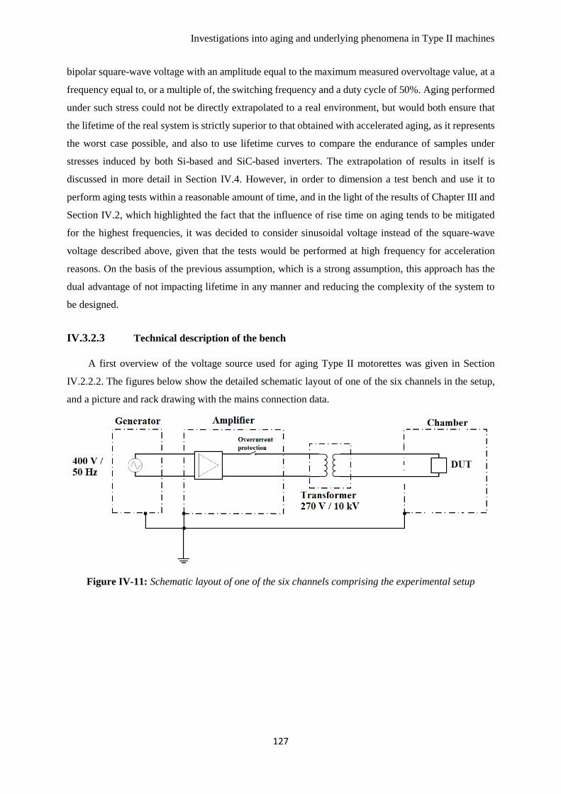
Investigations into aging and underlying phenomena in Type II machines
127
bipolar square-wave voltage with an amplitude equal to the maximum measured overvoltage value, at a
frequency equal to, or a multiple of, the switching frequency and a duty cycle of 50%. Aging performed
under such stress could not be directly extrapolated to a real environment, but would both ensure that
the lifetime of the real system is strictly superior to that obtained with accelerated aging, as it represents
the worst case possible, and also to use lifetime curves to compare the endurance of samples under
stresses induced by both Si-based and SiC-based inverters. The extrapolation of results in itself is
discussed in more detail in Section IV.4. However, in order to dimension a test bench and use it to
perform aging tests within a reasonable amount of time, and in the light of the results of Chapter III and
Section IV.2, which highlighted the fact that the influence of rise time on aging tends to be mitigated
for the highest frequencies, it was decided to consider sinusoidal voltage instead of the square-wave
voltage described above, given that the tests would be performed at high frequency for acceleration
reasons. On the basis of the previous assumption, which is a strong assumption, this approach has the
dual advantage of not impacting lifetime in any manner and reducing the complexity of the system to
be designed.
IV.3.2.3 Technical description of the bench
A first overview of the voltage source used for aging Type II motorettes was given in Section
IV.2.2.2. The figures below show the detailed schematic layout of one of the six channels in the setup,
and a picture and rack drawing with the mains connection data.
Figure IV-11: Schematic layout of one of the six channels comprising the experimental setup
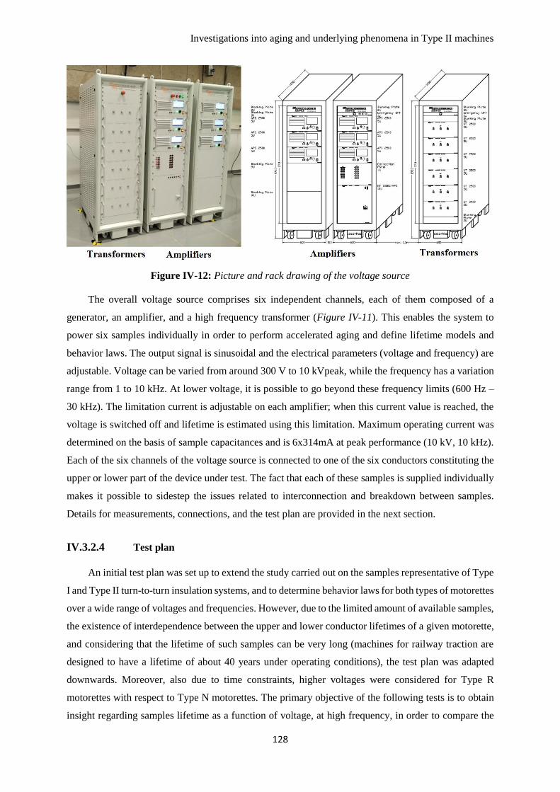
Investigations into aging and underlying phenomena in Type II machines
128
Figure IV-12: Picture and rack drawing of the voltage source
The overall voltage source comprises six independent channels, each of them composed of a
generator, an amplifier, and a high frequency transformer (Figure IV-11). This enables the system to
power six samples individually in order to perform accelerated aging and define lifetime models and
behavior laws. The output signal is sinusoidal and the electrical parameters (voltage and frequency) are
adjustable. Voltage can be varied from around 300 V to 10 kVpeak, while the frequency has a variation
range from 1 to 10 kHz. At lower voltage, it is possible to go beyond these frequency limits (600 Hz –
30 kHz). The limitation current is adjustable on each amplifier; when this current value is reached, the
voltage is switched off and lifetime is estimated using this limitation. Maximum operating current was
determined on the basis of sample capacitances and is 6x314mA at peak performance (10 kV, 10 kHz).
Each of the six channels of the voltage source is connected to one of the six conductors constituting the
upper or lower part of the device under test. The fact that each of these samples is supplied individually
makes it possible to sidestep the issues related to interconnection and breakdown between samples.
Details for measurements, connections, and the test plan are provided in the next section.
IV.3.2.4 Test plan
An initial test plan was set up to extend the study carried out on the samples representative of Type
I and Type II turn-to-turn insulation systems, and to determine behavior laws for both types of motorettes
over a wide range of voltages and frequencies. However, due to the limited amount of available samples,
the existence of interdependence between the upper and lower conductor lifetimes of a given motorette,
and considering that the lifetime of such samples can be very long (machines for railway traction are
designed to have a lifetime of about 40 years under operating conditions), the test plan was adapted
downwards. Moreover, also due to time constraints, higher voltages were considered for Type R
motorettes with respect to Type N motorettes. The primary objective of the following tests is to obtain
insight regarding samples lifetime as a function of voltage, at high frequency, in order to compare the
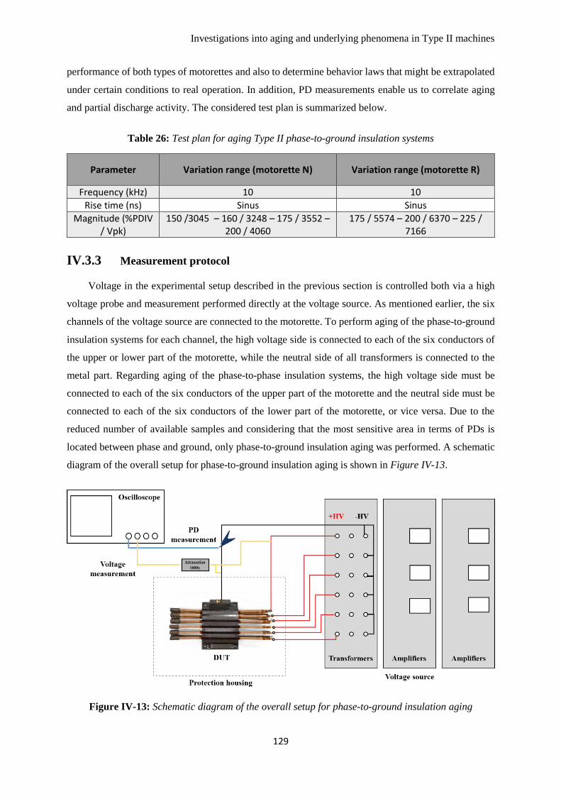
Investigations into aging and underlying phenomena in Type II machines
129
performance of both types of motorettes and also to determine behavior laws that might be extrapolated
under certain conditions to real operation. In addition, PD measurements enable us to correlate aging
and partial discharge activity. The considered test plan is summarized below.
Table 26: Test plan for aging Type II phase-to-ground insulation systems
Parameter Variation range (motorette N) Variation range (motorette R)
Frequency (kHz) 10 10
Rise time (ns) Sinus Sinus
Magnitude (%PDIV / Vpk)
150 /3045 – 160 / 3248 – 175 / 3552 – 200 / 4060
175 / 5574 – 200 / 6370 – 225 / 7166
IV.3.3 Measurement protocol
Voltage in the experimental setup described in the previous section is controlled both via a high
voltage probe and measurement performed directly at the voltage source. As mentioned earlier, the six
channels of the voltage source are connected to the motorette. To perform aging of the phase-to-ground
insulation systems for each channel, the high voltage side is connected to each of the six conductors of
the upper or lower part of the motorette, while the neutral side of all transformers is connected to the
metal part. Regarding aging of the phase-to-phase insulation systems, the high voltage side must be
connected to each of the six conductors of the upper part of the motorette and the neutral side must be
connected to each of the six conductors of the lower part of the motorette, or vice versa. Due to the
reduced number of available samples and considering that the most sensitive area in terms of PDs is
located between phase and ground, only phase-to-ground insulation aging was performed. A schematic
diagram of the overall setup for phase-to-ground insulation aging is shown in Figure IV-13.
Figure IV-13: Schematic diagram of the overall setup for phase-to-ground insulation aging
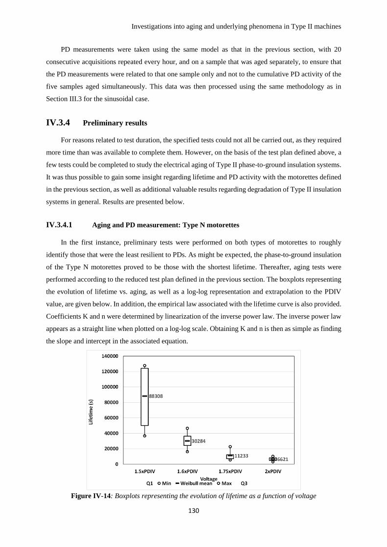
Investigations into aging and underlying phenomena in Type II machines
130
PD measurements were taken using the same model as that in the previous section, with 20
consecutive acquisitions repeated every hour, and on a sample that was aged separately, to ensure that
the PD measurements were related to that one sample only and not to the cumulative PD activity of the
five samples aged simultaneously. This data was then processed using the same methodology as in
Section III.3 for the sinusoidal case.
IV.3.4 Preliminary results
For reasons related to test duration, the specified tests could not all be carried out, as they required
more time than was available to complete them. However, on the basis of the test plan defined above, a
few tests could be completed to study the electrical aging of Type II phase-to-ground insulation systems.
It was thus possible to gain some insight regarding lifetime and PD activity with the motorettes defined
in the previous section, as well as additional valuable results regarding degradation of Type II insulation
systems in general. Results are presented below.
IV.3.4.1 Aging and PD measurement: Type N motorettes
In the first instance, preliminary tests were performed on both types of motorettes to roughly
identify those that were the least resilient to PDs. As might be expected, the phase-to-ground insulation
of the Type N motorettes proved to be those with the shortest lifetime. Thereafter, aging tests were
performed according to the reduced test plan defined in the previous section. The boxplots representing
the evolution of lifetime vs. aging, as well as a log-log representation and extrapolation to the PDIV
value, are given below. In addition, the empirical law associated with the lifetime curve is also provided.
Coefficients K and n were determined by linearization of the inverse power law. The inverse power law
appears as a straight line when plotted on a log-log scale. Obtaining K and n is then as simple as finding
the slope and intercept in the associated equation.
Figure IV-14: Boxplots representing the evolution of lifetime as a function of voltage
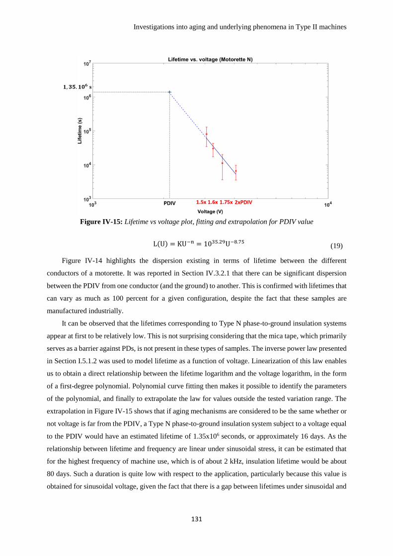
Investigations into aging and underlying phenomena in Type II machines
131
Figure IV-15: Lifetime vs voltage plot, fitting and extrapolation for PDIV value
L(U) = KU−n = 1035.29U−8.75 (19)
Figure IV-14 highlights the dispersion existing in terms of lifetime between the different
conductors of a motorette. It was reported in Section IV.3.2.1 that there can be significant dispersion
between the PDIV from one conductor (and the ground) to another. This is confirmed with lifetimes that
can vary as much as 100 percent for a given configuration, despite the fact that these samples are
manufactured industrially.
It can be observed that the lifetimes corresponding to Type N phase-to-ground insulation systems
appear at first to be relatively low. This is not surprising considering that the mica tape, which primarily
serves as a barrier against PDs, is not present in these types of samples. The inverse power law presented
in Section I.5.1.2 was used to model lifetime as a function of voltage. Linearization of this law enables
us to obtain a direct relationship between the lifetime logarithm and the voltage logarithm, in the form
of a first-degree polynomial. Polynomial curve fitting then makes it possible to identify the parameters
of the polynomial, and finally to extrapolate the law for values outside the tested variation range. The
extrapolation in Figure IV-15 shows that if aging mechanisms are considered to be the same whether or
not voltage is far from the PDIV, a Type N phase-to-ground insulation system subject to a voltage equal
to the PDIV would have an estimated lifetime of 1.35x10⁶ seconds, or approximately 16 days. As the
relationship between lifetime and frequency are linear under sinusoidal stress, it can be estimated that
for the highest frequency of machine use, which is of about 2 kHz, insulation lifetime would be about
80 days. Such a duration is quite low with respect to the application, particularly because this value is
obtained for sinusoidal voltage, given the fact that there is a gap between lifetimes under sinusoidal and
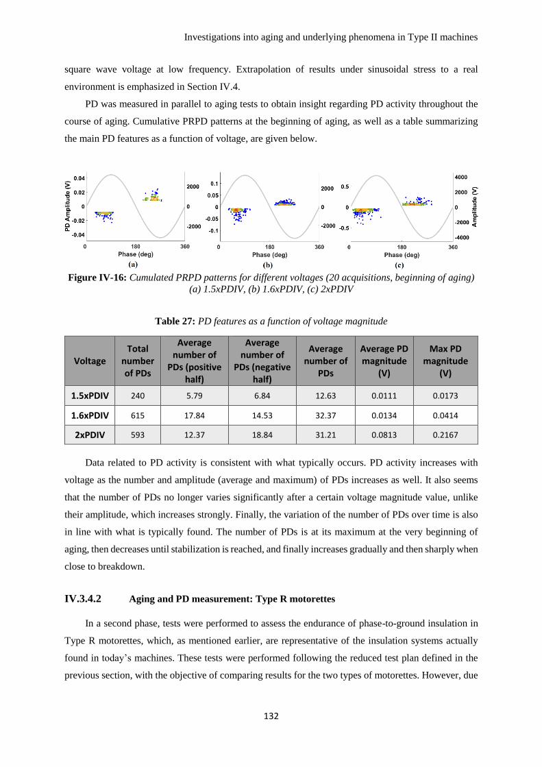
Investigations into aging and underlying phenomena in Type II machines
132
square wave voltage at low frequency. Extrapolation of results under sinusoidal stress to a real
environment is emphasized in Section IV.4.
PD was measured in parallel to aging tests to obtain insight regarding PD activity throughout the
course of aging. Cumulative PRPD patterns at the beginning of aging, as well as a table summarizing
the main PD features as a function of voltage, are given below.
Figure IV-16: Cumulated PRPD patterns for different voltages (20 acquisitions, beginning of aging)
(a) 1.5xPDIV, (b) 1.6xPDIV, (c) 2xPDIV
Table 27: PD features as a function of voltage magnitude
Voltage Total
number of PDs
Average number of
PDs (positive half)
Average number of
PDs (negative half)
Average number of
PDs
Average PD magnitude
(V)
Max PD magnitude
(V)
1.5xPDIV 240 5.79 6.84 12.63 0.0111 0.0173
1.6xPDIV 615 17.84 14.53 32.37 0.0134 0.0414
2xPDIV 593 12.37 18.84 31.21 0.0813 0.2167
Data related to PD activity is consistent with what typically occurs. PD activity increases with
voltage as the number and amplitude (average and maximum) of PDs increases as well. It also seems
that the number of PDs no longer varies significantly after a certain voltage magnitude value, unlike
their amplitude, which increases strongly. Finally, the variation of the number of PDs over time is also
in line with what is typically found. The number of PDs is at its maximum at the very beginning of
aging, then decreases until stabilization is reached, and finally increases gradually and then sharply when
close to breakdown.
IV.3.4.2 Aging and PD measurement: Type R motorettes
In a second phase, tests were performed to assess the endurance of phase-to-ground insulation in
Type R motorettes, which, as mentioned earlier, are representative of the insulation systems actually
found in today’s machines. These tests were performed following the reduced test plan defined in the
previous section, with the objective of comparing results for the two types of motorettes. However, due
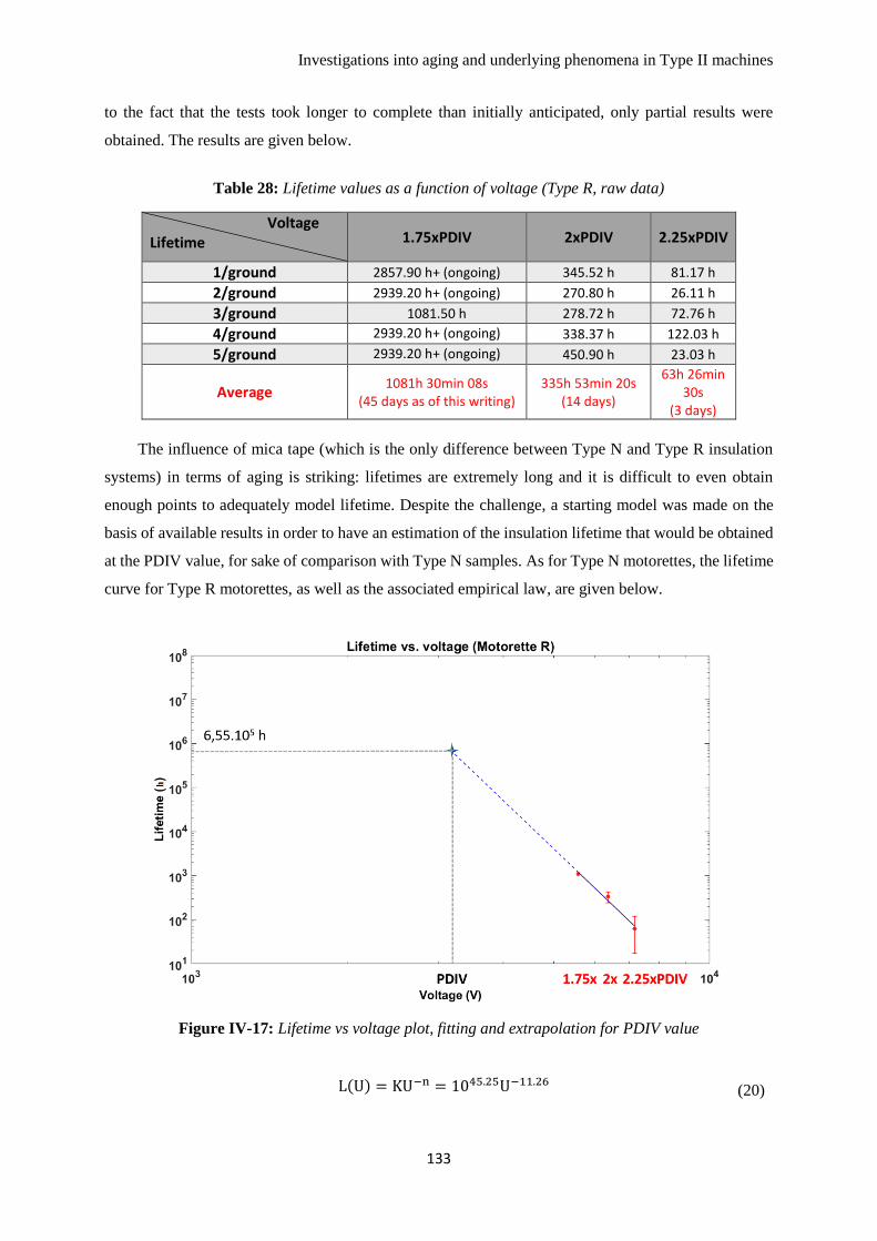
Investigations into aging and underlying phenomena in Type II machines
133
to the fact that the tests took longer to complete than initially anticipated, only partial results were
obtained. The results are given below.
Table 28: Lifetime values as a function of voltage (Type R, raw data)
Voltage Lifetime 1.75xPDIV 2xPDIV 2.25xPDIV
1/ground 2857.90 h+ (ongoing) 345.52 h 81.17 h
2/ground 2939.20 h+ (ongoing) 270.80 h 26.11 h
3/ground 1081.50 h 278.72 h 72.76 h
4/ground 2939.20 h+ (ongoing) 338.37 h 122.03 h
5/ground 2939.20 h+ (ongoing) 450.90 h 23.03 h
Average 1081h 30min 08s
(45 days as of this writing) 335h 53min 20s
(14 days)
63h 26min 30s
(3 days)
The influence of mica tape (which is the only difference between Type N and Type R insulation
systems) in terms of aging is striking: lifetimes are extremely long and it is difficult to even obtain
enough points to adequately model lifetime. Despite the challenge, a starting model was made on the
basis of available results in order to have an estimation of the insulation lifetime that would be obtained
at the PDIV value, for sake of comparison with Type N samples. As for Type N motorettes, the lifetime
curve for Type R motorettes, as well as the associated empirical law, are given below.
Figure IV-17: Lifetime vs voltage plot, fitting and extrapolation for PDIV value
L(U) = KU−n = 1045.25U−11.26 (20)
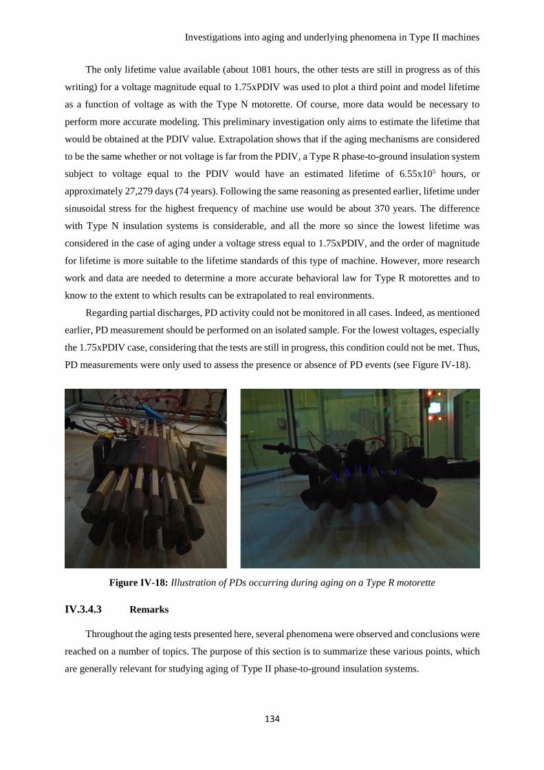
Investigations into aging and underlying phenomena in Type II machines
134
The only lifetime value available (about 1081 hours, the other tests are still in progress as of this
writing) for a voltage magnitude equal to 1.75xPDIV was used to plot a third point and model lifetime
as a function of voltage as with the Type N motorette. Of course, more data would be necessary to
perform more accurate modeling. This preliminary investigation only aims to estimate the lifetime that
would be obtained at the PDIV value. Extrapolation shows that if the aging mechanisms are considered
to be the same whether or not voltage is far from the PDIV, a Type R phase-to-ground insulation system
subject to voltage equal to the PDIV would have an estimated lifetime of 6.55x10⁵ hours, or
approximately 27,279 days (74 years). Following the same reasoning as presented earlier, lifetime under
sinusoidal stress for the highest frequency of machine use would be about 370 years. The difference
with Type N insulation systems is considerable, and all the more so since the lowest lifetime was
considered in the case of aging under a voltage stress equal to 1.75xPDIV, and the order of magnitude
for lifetime is more suitable to the lifetime standards of this type of machine. However, more research
work and data are needed to determine a more accurate behavioral law for Type R motorettes and to
know to the extent to which results can be extrapolated to real environments.
Regarding partial discharges, PD activity could not be monitored in all cases. Indeed, as mentioned
earlier, PD measurement should be performed on an isolated sample. For the lowest voltages, especially
the 1.75xPDIV case, considering that the tests are still in progress, this condition could not be met. Thus,
PD measurements were only used to assess the presence or absence of PD events (see Figure IV-18).
Figure IV-18: Illustration of PDs occurring during aging on a Type R motorette
IV.3.4.3 Remarks
Throughout the aging tests presented here, several phenomena were observed and conclusions were
reached on a number of topics. The purpose of this section is to summarize these various points, which
are generally relevant for studying aging of Type II phase-to-ground insulation systems.
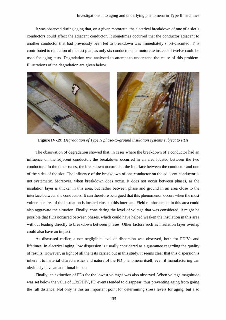
Investigations into aging and underlying phenomena in Type II machines
135
It was observed during aging that, on a given motorette, the electrical breakdown of one of a slot’s
conductors could affect the adjacent conductor. It sometimes occurred that the conductor adjacent to
another conductor that had previously been led to breakdown was immediately short-circuited. This
contributed to reduction of the test plan, as only six conductors per motorette instead of twelve could be
used for aging tests. Degradation was analyzed to attempt to understand the cause of this problem.
Illustrations of the degradation are given below.
Figure IV-19: Degradation of Type N phase-to-ground insulation systems subject to PDs
The observation of degradation showed that, in cases where the breakdown of a conductor had an
influence on the adjacent conductor, the breakdown occurred in an area located between the two
conductors. In the other cases, the breakdown occurred at the interface between the conductor and one
of the sides of the slot. The influence of the breakdown of one conductor on the adjacent conductor is
not systematic. Moreover, when breakdown does occur, it does not occur between phases, as the
insulation layer is thicker in this area, but rather between phase and ground in an area close to the
interface between the conductors. It can therefore be argued that this phenomenon occurs when the most
vulnerable area of the insulation is located close to this interface. Field reinforcement in this area could
also aggravate the situation. Finally, considering the level of voltage that was considered, it might be
possible that PDs occurred between phases, which could have helped weaken the insulation in this area
without leading directly to breakdown between phases. Other factors such as insulation layer overlap
could also have an impact.
As discussed earlier, a non-negligible level of dispersion was observed, both for PDIVs and
lifetimes. In electrical aging, low dispersion is usually considered as a guarantee regarding the quality
of results. However, in light of all the tests carried out in this study, it seems clear that this dispersion is
inherent to material characteristics and nature of the PD phenomena itself, even if manufacturing can
obviously have an additional impact.
Finally, an extinction of PDs for the lowest voltages was also observed. When voltage magnitude
was set below the value of 1.3xPDIV, PD events tended to disappear, thus preventing aging from going
the full distance. Not only is this an important point for determining stress levels for aging, but also
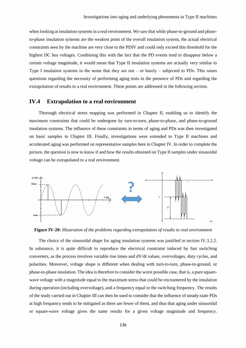
Investigations into aging and underlying phenomena in Type II machines
136
when looking at insulation systems in a real environment. We saw that while phase-to-ground and phase-
to-phase insulation systems are the weakest point of the overall insulation system, the actual electrical
constraints seen by the machine are very close to the PDIV and could only exceed this threshold for the
highest DC bus voltages. Combining this with the fact that the PD events tend to disappear below a
certain voltage magnitude, it would mean that Type II insulation systems are actually very similar to
Type I insulation systems in the sense that they are not – or barely – subjected to PDs. This raises
questions regarding the necessity of performing aging tests in the presence of PDs and regarding the
extrapolation of results to a real environment. These points are addressed in the following section.
IV.4 Extrapolation to a real environment
Thorough electrical stress mapping was performed in Chapter II, enabling us to identify the
maximum constraints that could be undergone by turn-to-turn, phase-to-phase, and phase-to-ground
insulation systems. The influence of these constraints in terms of aging and PDs was then investigated
on basic samples in Chapter III. Finally, investigations were extended to Type II machines and
accelerated aging was performed on representative samples here in Chapter IV. In order to complete the
picture, the question is now to know if and how the results obtained on Type II samples under sinusoidal
voltage can be extrapolated to a real environment.
Figure IV-20: Illustration of the problems regarding extrapolation of results to real environment
The choice of the sinusoidal shape for aging insulation systems was justified in section IV.3.2.2.
In substance, it is quite difficult to reproduce the electrical constraint induced by fast switching
converters, as the process involves variable rise times and dV/dt values, overvoltages, duty cycles, and
polarities. Moreover, voltage shape is different when dealing with turn-to-turn, phase-to-ground, or
phase-to-phase insulation. The idea is therefore to consider the worst possible case, that is, a pure square-
wave voltage with a magnitude equal to the maximum stress that could be encountered by the insulation
during operation (including overvoltage), and a frequency equal to the switching frequency. The results
of the study carried out in Chapter III can then be used to consider that the influence of steady-state PDs
at high frequency tends to be mitigated as there are fewer of them, and thus that aging under sinusoidal
or square-wave voltage gives the same results for a given voltage magnitude and frequency.
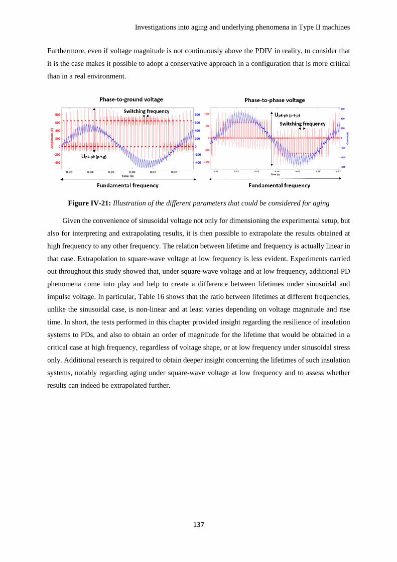
Investigations into aging and underlying phenomena in Type II machines
137
Furthermore, even if voltage magnitude is not continuously above the PDIV in reality, to consider that
it is the case makes it possible to adopt a conservative approach in a configuration that is more critical
than in a real environment.
Figure IV-21: Illustration of the different parameters that could be considered for aging
Given the convenience of sinusoidal voltage not only for dimensioning the experimental setup, but
also for interpreting and extrapolating results, it is then possible to extrapolate the results obtained at
high frequency to any other frequency. The relation between lifetime and frequency is actually linear in
that case. Extrapolation to square-wave voltage at low frequency is less evident. Experiments carried
out throughout this study showed that, under square-wave voltage and at low frequency, additional PD
phenomena come into play and help to create a difference between lifetimes under sinusoidal and
impulse voltage. In particular, Table 16 shows that the ratio between lifetimes at different frequencies,
unlike the sinusoidal case, is non-linear and at least varies depending on voltage magnitude and rise
time. In short, the tests performed in this chapter provided insight regarding the resilience of insulation
systems to PDs, and also to obtain an order of magnitude for the lifetime that would be obtained in a
critical case at high frequency, regardless of voltage shape, or at low frequency under sinusoidal stress
only. Additional research is required to obtain deeper insight concerning the lifetimes of such insulation
systems, notably regarding aging under square-wave voltage at low frequency and to assess whether
results can indeed be extrapolated further.
Investigations into aging and underlying phenomena in Type II machines
138
IV.5 Conclusion
The first tests conducted on Type II samples representative of turn-to-turn insulation systems led
to a number of conclusions that are outlined in this section. First, the PDIV and breakdown
measurements performed on those samples highlighted the fact that, in view of the electrical stress
identification conducted in Chapter II, turn-to-turn insulation systems are very unlikely to be subject to
partial discharges. The maximum turn-to-turn voltage either as an absolute figure or a percentage
remains very far away from the inception voltage, even for the fastest inverters.
Notwithstanding these results, aging tests were performed in the presence of PDs throughout the
entire aging process to assess the resilience of the Type II samples to PDs and to acknowledge whether
or not the results of the study conducted in Chapter III were transposable to Type II. It turns out that the
lifetime results confirmed established findings regarding the influence of rise time, frequency, and
amplitude on aging (duty cycle was not studied). PD measurements could not be taken, which is
unfortunate because they could have provided more insight into the mechanisms involved and confirmed
the approach that was proposed in the previous chapter.
Tests were performed in a second part, this time on samples representative of Type II phase-to-
ground and phase-to-phase insulation systems. Investigations carried out on these samples showed that
the PDIV values were quite high and that even in this area, the insulation systems would not be
continuously subject to PDs. The influence of mica tape was also highlighted in a comparison between
Type R and Type N motorettes, and then confirmed with aging tests performed under sinusoidal voltage.
To carry out these tests, a multi-channel, high voltage, high power, and high frequency experimental
setup was dimensioned accordingly and the voltage shape to use for aging was chosen based on the
results of Chapter III and by considering the worst case that could potentially be encountered by the
insulation system. Finally, a discussion about the aging of Type II insulation systems in general and the
extrapolation of results to a real environment were presented to provide overall coherence by
establishing the link between the different chapters in this work.

General conclusion
140
General conclusion
The rationalization of electrical energy in many applications, including transportation, leads to an
ever-growing number of questions and challenges, in particular regarding the reliability of systems and
especially that of insulating materials. In the railway sector, as well as in other areas, massive evolution
has been prompted to meet these new challenges. Voltage inverters based on pulse width modulation
are widely used for such applications that require controlling rotation speed. Si IGBT devices are used
today to create pulse width modulation. The use of IGBTs makes it possible to generate rising edges of
several kV/μs, and to reach switching frequencies up to several kHz. These improvements have helped
reducing switching losses and motor torque ripple but have led to the generation of more stressful
constraints. Moreover, the transition from conventional silicon-based components to new wide bandgap
components only exacerbated matters. De facto, there is a chance that the reliability of motors declines
dramatically, though more research needs to be carried out on the topic to confirm. The causes of motor
failures are due to different phenomena, but one of the main aging mechanisms is the erosion of the
various insulating materials induced by partial discharges. Systems may be designed to react differently
to these discharges but, in any case, the presence of PDs is an issue that affects the reliability of the
entire electromechanical chain.
In this context, we addressed the issues of partial discharges and aging mechanisms for insulation
systems used in rotating machines. A state of the art on degradation mechanisms and the systems on
which they appear was presented. The influence of electrical stress and control strategy on aging was
reviewed in detail and, finally, the aging phenomenon itself was defined and depicted.
The determination and impact of the existence of partial discharges in a railway traction system
using SiC-based components was established in three steps. The first step consisted of a test campaign
that sought to perform thorough electrical stress mapping depending on both geometric and electrical
parameters to analyze the influence of various parameters on electrical stress, and finally to perform
partial discharge measurements on a machine in real environment. We saw that the turn-to-turn voltage
values in this type of motor are low. With those voltages, power electronics and thus rising edges can
have little influence on the ignition of partial discharges between turns. Nevertheless, the use of fast-
switching SiC-based inverters causes an increase of overvoltages for phase-to-ground and phase-to-
phase voltages. These more stressful constraints eventually lead to an increase in partial discharge
activity between phases or between phase and ground. These insulation systems therefore constitute the
weakest point of the system in terms of reliability.
In a second step, an analysis of the impact of electrical stress on partial discharge features and
aging was presented. This phenomenological study offered an opportunity to precisely study the
different constituents of electrical stress in order to explain their influence on PD activity and
General conclusion
141
degradation. The study was carried out considering basic samples representative of Type I turn-to-turn
insulation systems. It was shown that these parameters have a non-negligible impact on aging, at
different levels. The impact of overvoltage is significant and all the more marked when it comes to
steady-state voltage magnitude. A coupled impact of rise time and frequency was observed: the effect
of rise time on aging tends to be mitigated at the highest frequencies. Finally, duty cycle and – indirectly
– pulse duration also seem to have an impact on aging. PD measurement during aging enabled us to link
these phenomena with the presence or absence of PDs during the steady part of the voltage. Those PDs,
which are additional to those usually found during the edges, could possibly explain the differences
induced by varying the different parameters.
Finally, the last chapter focused on reproducing the electrical constraints identified in the second
chapter on more complex samples representative of Type II insulation systems. This work had the dual
purpose of extending the results obtained for Type I systems to Type II systems, and studying the
lifetime and degradation of real insulation systems under stress. Studies performed on Type II samples
confirmed that the turn-to-turn insulation systems in Type II machines are very unlikely to be subject to
PDs. Moreover, they confirmed the results obtained on Type I samples regarding the influence of
electrical stress on aging. On the basis of these latter results, an experimental setup was specially
dimensioned to age samples representative of phase-to-phase and phase-to-ground insulation systems,
which were previously identified as higher risk areas. Despite the fact that, given the measured PDIV
values, these insulation systems seem to not be subject to PDs continuously, their resilience to PDs could
be assessed and it was possible to determine lifetime models and consider extrapolating these models to
real environments.
To go further on the subject, future work will be devoted to extending experiments on Type I and
Type II samples in efforts to understand the PD phenomena responsible for aging. Additional tests under
square-wave voltage at low frequency would also be necessary to try to find complete correlation
between aging under sinusoidal and square-wave voltage, and to refine the lifetime models and their
extrapolation to real environments. Finally, in the context of the global increase in voltage levels, which
does not only apply to the railway sector, another possible perspective could be to build on progress that
has already been made and study the aging of Type II insulation systems under aeronautical conditions
to anticipate the possible transition from Type I to Type II machines in other specialized fields.

References
143
References
[1] X. Roboam, “New trends and challenges of electrical networks embedded in ‘more electrical
aircraft,’” in 2011 IEEE International Symposium on Industrial Electronics, Jun. 2011, pp. 26–31, doi:
10.1109/ISIE.2011.5984130.
[2] P. Eremenko, “Building the Third Golden Age of Aerospace,” Airbus, 2017.
[3] R. Bartnikas and E. J. McMahon, Engineering Dielectrics Volume I: Corona measurement and
interpretation. ASTM STP 669, 1979.
[4] J. P. Novak and R. Bartnikas, “Effect of dielectric surfaces on the nature of partial discharges,”
IEEE Trans. Dielectr. Electr. Insul., vol. 7, no. 1, pp. 146–151, Feb. 2000, doi: 10.1109/94.839353.
[5] F. Paschen, “Uber die zum Funkenübergang in Luft, Wasserstoff und Kohlensäure bei
verschiedenen Drucken erforderliche Potentialdifferenz,” Ann. Phys., vol. 273, no. 5, pp. 69–96, 1889,
doi: 10.1002/andp.18892730505.
[6] Y. P. Raizer, Gas discharge physics. Berlin, Germany: Springer, 1991.
[7] R. Bartnikas and J. P. Novak, “Effect of overvoltage on the risetime and amplitude of PD
pulses,” IEEE Trans. Dielectr. Electr. Insul., vol. 2, no. 4, pp. 557–566, Aug. 1995, doi:
10.1109/94.407021.
[8] R. Bartnikas, “Some Observations on the Character of Corona Discharges in Short Gap Spaces,”
IEEE Trans. Electr. Insul., vol. EI-6, no. 2, pp. 63–75, Jun. 1971, doi: 10.1109/TEI.1971.299156.
[9] C. Abadie, “On-line non-intrusive partial discharges detection in aeronautical systems,” UT3
Paul Sabatier, Toulouse, 2017.
[10] C. Abadie, T. Billard, and T. Lebey, “Partial discharges in motor fed by inverter: from detection
to winding configuration,” IEEE Trans. Ind. Appl., pp. 1–1, 2018, doi: 10.1109/TIA.2018.2874875.
[11] G. C. Montanari, A. Cavallini, F. Ciani, and A. Contin, “Accelerated aging, partial discharges
and breakdown of Type II turn-to-turn insulation system of rotating machines,” in 2016 IEEE Electrical
Insulation Conference (EIC), Jun. 2016, pp. 190–193, doi: 10.1109/EIC.2016.7548692.
[12] M. Hikita, S. Okabe, H. Murase, and H. Okubo, “Cross-equipment Evaluation of Partial
Discharge Measurement and Diagnosis Techniques in Electric Power Apparatus for Transmission and
Distribution,” IEEE Trans. Dielectr. Electr. Insul., vol. 15, no. 2, pp. 505–518, Apr. 2008, doi:
10.1109/TDEI.2008.4483471.
[13] R. Giussani, I. Cotton, and R. Sloan, “Detection of corona with RF methods and spectra
analysis,” in 2012 IEEE International Symposium on Electrical Insulation, Jun. 2012, pp. 132–136, doi:
10.1109/ELINSL.2012.6251442.
[14] “IEC 60034 - Rotating electrical machines - Part 18-41: Partial discharge free electrical
insulation systems (Type I) used in rotating electrical machines fed from voltage converters -
Qualification and quality control tests.”
References
144
[15] “IEC 60034 - Rotating electrical machines - Part 18-42: Partial discharge resistant electrical
insulation systems (Type II) used in rotating electrical machines fed from voltage converters -
Qualification tests.”
[16] I. Culbert, “Experience with partial discharge testing during voltage surges as required by IEC
60034-18-41 and 60034-18-42,” in Conference Record of 2009 Annual Pulp and Paper Industry
Technical Conference, Jun. 2009, pp. 156–160, doi: 10.1109/PAPCON.2009.5185418.
[17] D. R. Johnston and M. Markovitz, “Corona-resistant insulation, electrical conductors covered
therewith and dynamoelectric machines and transformers incorporating components of such insulated
conductors,” 4,760,296, Jul. 26, 1988.
[18] F. Guastavino, A. Ratto, and G. Coletti, “Twisted pair specimens insulated by conventional and
nanocomposite enamel: Life curves and PD patterns,” in 2009 9th IEEE Conference on Nanotechnology
(IEEE-NANO), Jul. 2009, pp. 183–186.
[19] F. Guastavino, A. Ratto, E. Torello, and G. Biondi, “Aging Tests on Nanostructured Enamels
for Winding Wire Insulation,” IEEE Trans. Ind. Electron., vol. 61, no. 10, pp. 5550–5557, Oct. 2014,
doi: 10.1109/TIE.2014.2301736.
[20] D. Fabiani, G. C. Montanari, and A. Contin, “Aging acceleration of insulating materials for
electrical machine windings supplied by PWM in the presence and in the absence of partial discharges,”
in Proceedings of the 2001 IEEE 7th International Conference on Solid Dielectrics, 2001. ICSD ’01,
2001, pp. 283–286, doi: 10.1109/ICSD.2001.955625.
[21] F. Costa, “Les onduleurs de tension en commutation commandée.” .
[22] M. R. Islam, Y. Guo, and J. G. Zhu, “Power Converter Topologies for Grid-Integrated Medium-
Voltage Applications,” 2014, pp. 51–107.
[23] S. K. Sahoo, A. Ramulu, S. Batta, and S. Duggal, “Performance analysis and simulation of three
phase voltage source inverter using basic PWM techniques,” in IET Chennai 3rd International on
Sustainable Energy and Intelligent Systems (SEISCON 2012), Dec. 2012, pp. 1–7, doi:
10.1049/cp.2012.2223.
[24] F. Guastavino, G. Coletti, A. Dardano, and E. Torello, “Life tests on twisted pairs subjected to
PWM-like voltages,” in Proceedings of the 2004 IEEE International Conference on Solid Dielectrics,
2004. ICSD 2004., Jul. 2004, vol. 2, pp. 860-863 Vol.2, doi: 10.1109/ICSD.2004.1350567.
[25] F. Guastavino, D. Cordano, E. Torello, and G. Secondo, “Electrical aging tests on different kind
of insulating systems adopted for induction stator motor,” in 2015 IEEE Conference on Electrical
Insulation and Dielectric Phenomena (CEIDP), Oct. 2015, pp. 808–811, doi:
10.1109/CEIDP.2015.7352068.
[26] D. Roger and S. Savin, “Fiabilité des systèmes d’isolation électrique des machines connectées
à des convertisseurs SiC et GaN et des busbars laminés : Problématique, état de l’art, objectifs et
investigations préliminaires.” 2014.
References
145
[27] V. Mihaila, “Nouvelle conception des bobinages statoriques des machines à courant alternatif
pour réduire les effets négatifs des dV/dt,” Université d’Artois, Béthune, 2011.
[28] B. Taghia, T. Billard, J. Carayon, D. Malec, H. Piquet, and A. Belinger, “Investigations on
Partial Discharges Risk in Aeronautical Rotating Machine Fed by HVDC 540VDC Network,” in 2018
IEEE Electrical Insulation Conference (EIC), Jun. 2018, pp. 491–494, doi: 10.1109/EIC.2018.8481115.
[29] C. Zoeller, T. M. Wolbank, and M. A. Vogelsberger, “Inverter-fed drive stator insulation
monitoring based on reflection phenomena stimulated by voltage step excitation,” in 2016 IEEE Energy
Conversion Congress and Exposition (ECCE), Sep. 2016, pp. 1–8, doi: 10.1109/ECCE.2016.7855213.
[30] M. Fenger, S. R. Campbell, and G. Gao, “The impact of surge voltage rise-time on PD inception
voltage in random wound motors of different designs,” in 2001 Annual Report Conference on Electrical
Insulation and Dielectric Phenomena (Cat. No.01CH37225), 2001, pp. 352–355, doi:
10.1109/CEIDP.2001.963555.
[31] M. Fenger, G. Stone, and S. Campbell, “Partial discharges on low voltage stator windings
subjected to voltage surges from adjustable speed drives,” in 2002 International Conference on Power
Electronics, Machines and Drives (Conf. Publ. No. 487), Jun. 2002, pp. 298–302, doi:
10.1049/cp:20020132.
[32] M. Tozzi, G. C. Montanari, D. Fabiani, A. Cavallini, and G. Gao, “Off-line and on-line pd
measurements on induction motors fed by power electronic impulses,” in 2009 IEEE Electrical
Insulation Conference, May 2009, pp. 420–424, doi: 10.1109/EIC.2009.5166383.
[33] G. Robles, J. M. Martinez-Tarifa, M. V. Rojas-Moreno, and J. Sanz-Feito, “Inductive Sensor
for Measuring High Frequency Partial Discharges Within Electrical Insulation,” IEEE Trans. Instrum.
Meas., vol. 58, no. 11, pp. 3907–3913, Nov. 2009, doi: 10.1109/TIM.2009.2021239.
[34] P. Wang, A. Cavallini, and G. C. Montanari, “The influence of square voltage rise time on partial
discharge spectra,” in 2012 Annual Report Conference on Electrical Insulation and Dielectric
Phenomena, Oct. 2012, pp. 129–132, doi: 10.1109/CEIDP.2012.6378738.
[35] S. Mao, T. Wu, X. Lu, J. Popovic, and J. A. Ferreira, “High frequency high voltage power
conversion with silicon carbide power semiconductor devices,” in 2016 6th Electronic System-
Integration Technology Conference (ESTC), Sep. 2016, pp. 1–5, doi: 10.1109/ESTC.2016.7764721.
[36] C. Zoeller, M. A. Vogelsberger, T. M. Wolbank, and H. Ertl, “Impact of SiC semiconductors
switching transition speed on insulation health state monitoring of traction machines,” IET Power
Electron., vol. 9, no. 15, pp. 2769–2775, 2016, doi: 10.1049/iet-pel.2015.0988.
[37] C. Zoeller, M. A. Vogelsberger, and T. M. Wolbank, “Influence of parasitic capacitances of
IGBT inverter on insulation condition monitoring of traction machines based on current signal transients
analysis,” in 2016 18th European Conference on Power Electronics and Applications (EPE’16 ECCE
Europe), Sep. 2016, pp. 1–9, doi: 10.1109/EPE.2016.7695580.
[38] F. Salameh, “Méthodes de modélisation statistique de la durée de vie des composants en génie
électrique,” Institut National Polytechnique, Toulouse, 2016.
References
146
[39] G. C. Stone and J. F. Lawless, “Weibull statistical analysis of aging tests on solid electrical
insulation,” in 1978 IEEE International Conference on Electrical Insulation, Jun. 1978, pp. 13–16, doi:
10.1109/EIC.1978.7463562.
[40] C. Kaijiang, W. Guangning, Z. Liren, G. Xiaoxia, L. Kegang, and G. Bo, “Insulation life-span
models for electrical and thermal aging under continuous high square impulses voltage,” in 2009 IEEE
9th International Conference on the Properties and Applications of Dielectric Materials, Jul. 2009, pp.
285–288, doi: 10.1109/ICPADM.2009.5252428.
[41] G. Cannatà, S. De Caro, S. Panarello, T. Scimone, A. Testa, and S. Russo, “Reliability
Assessment of Avalanche Mode Operating Power MOSFETs through Coffin Manson Law based
Mathematical Models,” in Automation and Motion 2014 International Symposium on Power
Electronics, Electrical Drives, Jun. 2014, pp. 139–145, doi: 10.1109/SPEEDAM.2014.6872071.
[42] M. Farahani, E. Gockenbach, H. Borsi, and M. Kaufhold, “Behavior of a Machine Insulation
System during Accelerated Aging Tests,” in Conference Record of the 2008 IEEE International
Symposium on Electrical Insulation, Jun. 2008, pp. 404–407, doi: 10.1109/ELINSL.2008.4570359.
[43] J. P. Bellomo, T. Lebey, J. M. Oraison, and F. Peltier, “Study of the aging of different dielectrics
under specific electrical constraints,” in Proceedings of 1994 4th International Conference on
Properties and Applications of Dielectric Materials (ICPADM), Jul. 1994, vol. 2, pp. 796–799 vol.2,
doi: 10.1109/ICPADM.1994.414131.
[44] M. Farahani, H. Borsi, E. Gockenbach, and M. Kaufhold, “Partial discharge and dissipation
factor behavior of model insulating systems for high voltage rotating machines under different stresses,”
IEEE Electr. Insul. Mag., vol. 21, no. 5, pp. 5–19, Sep. 2005, doi: 10.1109/MEI.2005.1513425.
[45] A. Altmann, K. Engel, D. Peier, and K. Senske, “Partial Discharge Analysis During Accelerated
Aging Tests For The Optimization Of HV Electrical Machine Insulation,” in Proceedings of the 6th
International Conference on Optimization of Electrical and Electronic Equipments, May 1998, vol. 1,
pp. 181–184, doi: 10.1109/OPTIM.1998.710468.
[46] P. Wang, G. C. Montanari, and A. Cavallini, “Partial Discharge Phenomenology and Induced
Aging Behavior in Rotating Machines Controlled by Power Electronics,” IEEE Trans. Ind. Electron.,
vol. 61, no. 12, pp. 7105–7112, Dec. 2014, doi: 10.1109/TIE.2014.2320226.
[47] K. Wu, T. Okamoto, and Y. Suzuoki, “Transition of Partial Discharge Behavior with Aging
under Square-wave AC Voltage,” in 2006 IEEE 8th International Conference on Properties
applications of Dielectric Materials, Jun. 2006, pp. 36–39, doi: 10.1109/ICPADM.2006.284111.
[48] E. Sili, J. P. Cambronne, N. Naude, and R. Khazaka, “Polyimide lifetime under partial discharge
aging: effects of temperature, pressure and humidity,” IEEE Trans. Dielectr. Electr. Insul., vol. 20, no.
2, pp. 435–442, Apr. 2013, doi: 10.1109/TDEI.2013.6508745.
[49] L. Verardi, D. Fabiani, G. C. Montanari, and V. Plaček, “Electrical aging markers for low-
voltage cable insulation wiring of nuclear power plants,” in 2012 IEEE 10th International Conference
References
147
on the Properties and Applications of Dielectric Materials, Jul. 2012, pp. 1–4, doi:
10.1109/ICPADM.2012.6318966.
[50] C. Perrier, M.-L. Coulibaly, and M. Marugan, “Efficiency of aging markers for different
transformer insulation systems,” in 2016 IEEE International Conference on Dielectrics (ICD), Jul.
2016, vol. 2, pp. 824–827, doi: 10.1109/ICD.2016.7547743.
[51] P. Wang, N. Yang, C. Zheng, and Y. Li, “Effect of repetitive impulsive and square wave voltage
frequency on partial discharge features,” in 2018 12th International Conference on the Properties and
Applications of Dielectric Materials (ICPADM), May 2018, pp. 152–155, doi:
10.1109/ICPADM.2018.8401153.
[52] S. Matsumoto, and D. Nagaba, and T. Ogiya, “Partial discharge characteristics of twisted
magnet wire under high frequency AC voltage,” in Proceedings of 2014 International Symposium on
Electrical Insulating Materials, Jun. 2014, pp. 57–60, doi: 10.1109/ISEIM.2014.6870719.
[53] A. Cavallini, V. Krotov, G. C. Montanari, P. H. F. Morshuis, and L. E. Mariut, “The role of
supply frequency in the evaluation of partial discharge inception voltage in XLPE-embedded cavities,”
in 2012 Annual Report Conference on Electrical Insulation and Dielectric Phenomena, Oct. 2012, pp.
487–490, doi: 10.1109/CEIDP.2012.6378826.
[54] D. Fabiani, G. C. Montanari, A. Cavallini, and G. Mazzanti, “Relation between space charge
accumulation and partial discharge activity in enameled wires under PWM-like voltage waveforms,”
IEEE Trans. Dielectr. Electr. Insul., vol. 11, no. 3, pp. 393–405, Jun. 2004, doi:
10.1109/TDEI.2004.1306718.
[55] L. Lusuardi, A. Cavallini, A. Caprara, F. Bardelli, and A. Cattazzo, “The Impact of Test Voltage
Waveform in Determining the Repetitive Partial Discharge Inception Voltage of Type I Turn/Turn
Insulation Used in Inverter-Fed Induction Motors,” in 2018 IEEE Electrical Insulation Conference
(EIC), Jun. 2018, pp. 478–481, doi: 10.1109/EIC.2018.8481018.
[56] J. Ramirez, E. D. Silva, J. Sanz, J. Bermudez, and J. Rodriguez, “Comparison of the accelerated
aging under different thermal cycles and voltages impulses in XLPE cables,” in CEIDP ’05. 2005
Annual Report Conference on Electrical Insulation and Dielectric Phenomena, 2005., Oct. 2005, pp.
229–232, doi: 10.1109/CEIDP.2005.1560663.
[57] F. Guastavino, A. Dardano, A. Ratto, and E. Torello, “Electrical aging test on twisted pair
specimens under different environmental conditions,” in 2009 IEEE Conference on Electrical Insulation
and Dielectric Phenomena, Oct. 2009, pp. 81–84, doi: 10.1109/CEIDP.2009.5377744.
[58] G. Pietrini, D. Barater, F. Immovilli, A. Cavallini, and G. Franceschini, “Multi-stress lifetime
model of the winding insulation of electrical machines,” in 2017 IEEE Workshop on Electrical Machines
Design, Control and Diagnosis (WEMDCD), Apr. 2017, pp. 268–274, doi:
10.1109/WEMDCD.2017.7947758.
[59] M. Szczepanski, D. Malec, P. Maussion, B. Petitgas, and P. Manfé, “Use of Design of
Experiments (DoE) predictive models as a method of comparison of enameled wires used in low voltage
References
148
inverter-fed motors,” in 2018 IEEE Industry Applications Society Annual Meeting (IAS), Sep. 2018, pp.
1–8, doi: 10.1109/IAS.2018.8544548.
[60] K. Kimura, “Multistress aging of machine insulation systems,” in Proceedings of 1995
Conference on Electrical Insulation and Dielectric Phenomena, Oct. 1995, pp. 205–210, doi:
10.1109/CEIDP.1995.483611.
[61] T. S. Ramu, “Degradation of HV generator insulation under mechanical, electrical and thermal
stresses,” in IEEE International Symposium on Electrical Insulation, Jun. 1990, pp. 21–24, doi:
10.1109/ELINSL.1990.109699.
[62] J. P. Bellomo, T. Lebey, J. M. Oraison, and F. Peltier, “Characterisation of voltage shapes acting
on the insulation of rotating machines supplied by inverters,” in Proceedings of 1994 4th International
Conference on Properties and Applications of Dielectric Materials (ICPADM), Jul. 1994, vol. 2, pp.
792–795 vol.2, doi: 10.1109/ICPADM.1994.414130.
[63] M. Melfi, A. M. J. Sung, S. Bell, and G. L. Skibinski, “Effect of surge voltage risetime on the
insulation of low-voltage machines fed by PWM converters,” IEEE Trans. Ind. Appl., vol. 34, no. 4, pp.
766–775, Aug. 1998, doi: 10.1109/28.703971.
[64] J. P. Bellomo, T. Lebey, J. M. Oraison, and F. Peltier, “Electrical aging of stator insulation of
low voltage rotating machines supplied by inverters,” in Conference Record of the 1996 IEEE
International Symposium on Electrical Insulation, Jun. 1996, vol. 1, pp. 210–213 vol.1, doi:
10.1109/ELINSL.1996.549319.
[65] J. P. Bellomo, P. Castelan, and T. Lebey, “The effect of pulsed voltages on dielectric material
properties,” IEEE Trans. Dielectr. Electr. Insul., vol. 6, no. 1, pp. 20–26, Feb. 1999, doi:
10.1109/94.752005.
[66] L. Gubbala, A. von Jouanne, P. Enjeti, C. Singh, and H. Toliyat, “Voltage distribution in the
windings of an AC motor subjected to high dV/dt PWM voltages,” in Proceedings of PESC ’95 - Power
Electronics Specialist Conference, Atlanta, GA, USA, 1995, vol. 1, pp. 579–585, doi:
10.1109/PESC.1995.474867.
[67] G. Stone, S. Campbell, and S. Tetreault, “Inverter-fed drives: which motor stators are at risk?,”
IEEE Ind. Appl. Mag., vol. 6, no. 5, pp. 17–22, Sep. 2000, doi: 10.1109/2943.863631.
[68] H. Provencher, C. Millet, and S. Noel, “Analysis of turn insulation degradation under voltage
surge stress,” in 2016 IEEE Electrical Insulation Conference (EIC), Jun. 2016, pp. 409–413, doi:
10.1109/EIC.2016.7548625.
[69] M. Denk and M. M. Bakran, “Partial Discharge Measurement in a Motor Winding Fed by a SiC
Inverter - How Critical is High dV/dt Really?,” in PCIM Europe 2018; International Exhibition and
Conference for Power Electronics, Intelligent Motion, Renewable Energy and Energy Management,
Jun. 2018, pp. 1–6.
References
149
[70] T. Billard, T. Lebey, and F. Fresnet, “Partial discharge in electric motor fed by a PWM inverter:
off-line and on-line detection,” IEEE Trans. Dielectr. Electr. Insul., vol. 21, no. 3, pp. 1235–1242, Jun.
2014, doi: 10.1109/TDEI.2014.6832270.
[71] G. C. Stone, H. G. Sedding, and C. Chan, “Experience with on-line partial discharge
measurement in high voltage inverter fed motors,” in 2016 Petroleum and Chemical Industry Technical
Conference (PCIC), Sep. 2016, pp. 1–7, doi: 10.1109/PCICON.2016.7589241.
[72] C. Abadie, T. Billard, and T. Lebey, “Influence of pressure on partial discharge spectra,” in
2016 IEEE Electrical Insulation Conference (EIC), Jun. 2016, pp. 507–510, doi:
10.1109/EIC.2016.7548648.
[73] F. Guastavino, A. Dardano, and E. Torello, “Measuring partial discharges under pulsed voltage
conditions,” IEEE Trans. Dielectr. Electr. Insul., vol. 15, no. 6, Art. no. 6, Dec. 2008, doi:
10.1109/TDEI.2008.4712668.
[74] F. Sahlén, G. Paulsson, and E. Mårtensson, “Life-time investigation of mica-based insulation
for high voltage machines subjected to converter-like voltages,” in 2016 IEEE Electrical Insulation
Conference (EIC), Jun. 2016, pp. 460–463, doi: 10.1109/EIC.2016.7548637.
[75] J. Shao, “New thinking and methodologies on reliability engineering,” in 2009 8th International
Conference on Reliability, Maintainability and Safety, Chengdu, China, Jul. 2009, pp. 149–153, doi:
10.1109/ICRMS.2009.5270221.
[76] A. Barnard, “Ten things you should know about HALT & HASS,” in 2012 Proceedings Annual
Reliability and Maintainability Symposium, Reno, NV, USA, Jan. 2012, pp. 1–6, doi:
10.1109/RAMS.2012.6175457.
[77] “IEC 62068:2013: Electrical insulating materials and systems - General method of evaluation
of electrical endurance under repetitive voltage impulses.” .
[78] “IEC 60851-5: Winding wires - Test methods - Part 5: Electrical properties.” .
[79] K. Kimura, S. Ushirone, T. Koyanagi, and M. Hikita, “PDIV characteristics of twisted-pair of
magnet wires with repetitive impulse voltage,” IEEE Trans. Dielectr. Electr. Insul., vol. 14, no. 3, pp.
744–750, Jun. 2007, doi: 10.1109/TDEI.2007.369539.
[80] A. Cavallini, E. Lindell, G. C. Montanari, and M. Tozzi, “Inception of partial discharges under
repetitive square voltages: Effect of voltage waveform and repetition rate on PDIV and RPDIV,” in
2010 Annual Report Conference on Electrical Insulation and Dielectic Phenomena, West Lafayette, IN,
Oct. 2010, pp. 1–4, doi: 10.1109/CEIDP.2010.5724033.
[81] D. Goetz, H. Putter, F. Petzold, and S. Markalous, “PD characteristics under the aspect of
different voltage wave shapes and frequencies,” in 2016 Diagnostic of Electrical Machines and
Insulating Systems in Electrical Engineering (DEMISEE), Papradno, Slovakia, Jun. 2016, pp. 94–98,
doi: 10.1109/DEMISEE.2016.7530474.
References
150
[82] P. Wang, A. Cavallini, and G. C. Montanari, “The influence of repetitive square wave voltage
parameters on enameled wire endurance,” IEEE Trans. Dielectr. Electr. Insul., vol. 21, no. 3, pp. 1276–
1284, Jun. 2014, doi: 10.1109/TDEI.2014.6832275.
[83] F. Guastavino, G. Coletti, and E. Torello, “Twisted pairs specimens subjected to several
waveform voltages in presence of partial discharges,” in Annual Report Conference on Electrical
Insulation and Dielectric Phenomena, 2002, pp. 450–453, doi: 10.1109/CEIDP.2002.1048831.
[84] Tao Liu, Yi Xiao, Yangfei Lu, Xuwei Huang, Qingmin Li, and Zhongdong Wang, “Effect of
voltage frequency on surface discharge characteristics and aging process,” in 2017 IEEE Electrical
Insulation Conference (EIC), Baltimore, MD, USA, Jun. 2017, pp. 463–466, doi:
10.1109/EIC.2017.8004606.
[85] I. Radu, R. Bartnikas, and M. R. Wertheimer, “Frequency and voltage dependence of glow and
pseudoglow discharges in helium under atmospheric pressure,” IEEE Trans. Plasma Sci., vol. 31, no. 6,
pp. 1363–1378, Dec. 2003, doi: 10.1109/TPS.2003.820970.
[86] R. Miller and I. A. Black, “Partial discharge measurement’s over the frequency range 0.1 Hz to
50 Hz,” in 1976 IEEE International Conference on Electrical Insulation, Montreal, Quebec, Canada,
Jun. 1976, pp. 307–310, doi: 10.1109/EIC.1976.7464225.
[87] T. Billard, T. Lebey, A. Belinger, N. Naude, and N. Gherardi, “On the nature of the discharges
in samples fed by bipolar pulse like voltage and its possible impact on the detection of partial discharge
in machines fed by inverter,” in Proceedings of 2014 International Symposium on Electrical Insulating
Materials, Niigata, Jun. 2014, pp. 200–203, doi: 10.1109/ISEIM.2014.6870753.