Embed Size (px)
DESCRIPTION
Detectors and Analog Electronics. Bill Crain The Aerospace Corporation 310-336-8530 [email protected]. Introduction. Design Overview Requirements Flowdown Detector Specification Signals, Noise, and Processing Board Descriptions Interface Diagram Power Consumption Trade Studies - PowerPoint PPT Presentation
Citation preview
Cosmic RAy Telescope for the Effects of RadiationBill Crain, PDR Slide 1 28 September 2005
Detectors and Analog Electronics
Bill Crain
The Aerospace Corporation
310-336-8530
Cosmic RAy Telescope for the Effects of RadiationBill Crain, PDR Slide 2 28 September 2005
Introduction
• Design Overview
• Requirements Flowdown
• Detector Specification
• Signals, Noise, and Processing
• Board Descriptions
• Interface Diagram
• Power Consumption
• Trade Studies
• Summary
Cosmic RAy Telescope for the Effects of RadiationBill Crain, PDR Slide 3 28 September 2005
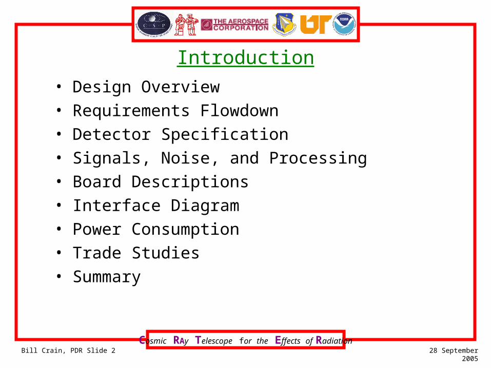
Detector Electronics Design Overview
• Electronic Board Designs– Telescope Board
– Analog Processing Board (APB) in E-box
• Heritage approach from Polar CEPPAD/IPS unchanged from proposal– Linear pulse processing system with Amptek front-end
– Circuits designed specifically for CRaTER requirements
• Functional requirements summary– Measure LET of high LET particles in thin detectors
– Measure LET of low LET particles in thick detectors
– Provide good resolution for TEP effects
– Robust to temperature drift and environments
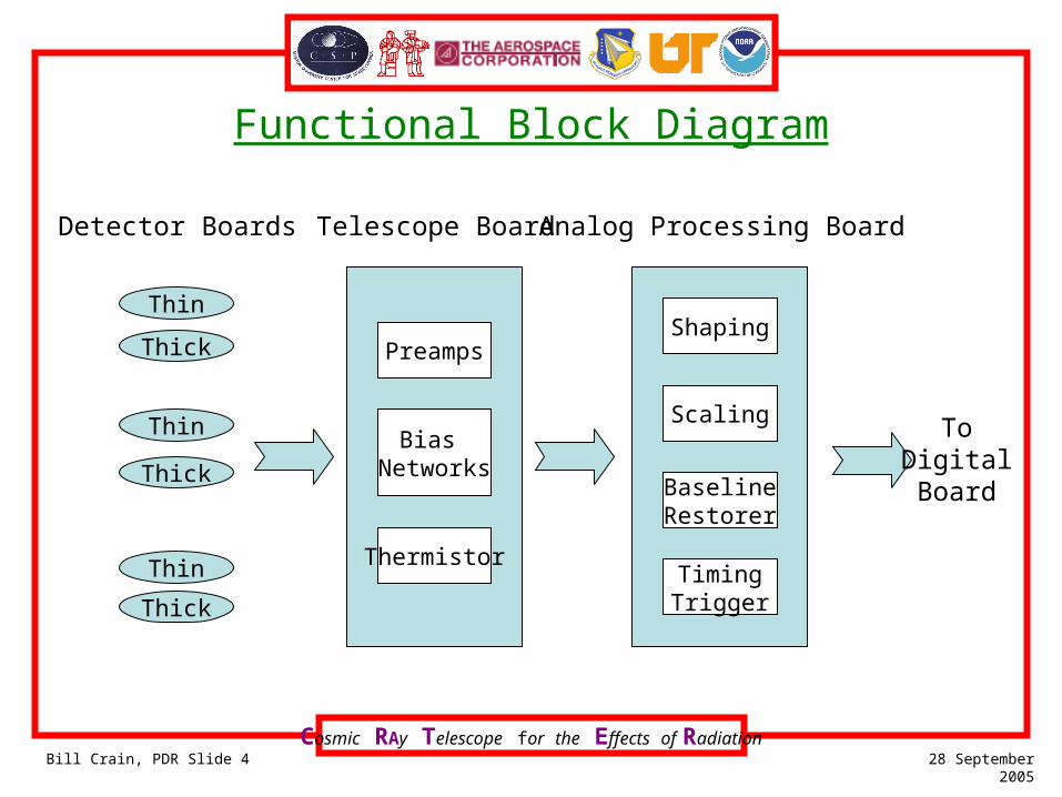
Cosmic RAy Telescope for the Effects of RadiationBill Crain, PDR Slide 4 28 September 2005
Thin
Thick
Thin
Thick
Thin
Thick
Preamps
Bias Networks
Thermistor
Telescope Board Analog Processing Board
Shaping
Scaling
BaselineRestorer
TimingTrigger
Detector Boards
ToDigitalBoard
Functional Block Diagram
Cosmic RAy Telescope for the Effects of RadiationBill Crain, PDR Slide 5 28 September 2005
Analog Signal Flow Diagram
• Single fixed gain, linear transfer function
• All detector channels use same topology
Analog PulseSignals
dv/dt &Pole-Zero
Cancellation
ShapingAmp
Amp
BaselineRestorer
Preamp
TimingDiscrim.
SiliconDetector
BiasNetwork
TestPulser
ScalingAmp
Digital TimingSignals
Cosmic RAy Telescope for the Effects of RadiationBill Crain, PDR Slide 6 28 September 2005
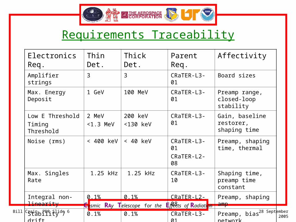
Requirements Traceability
Electronics Req. Thin Det. Thick Det. Parent Req. Affectivity
Amplifier strings 3 3 CRaTER-L3-01 Board sizes
Max. Energy Deposit 1 GeV 100 MeV CRaTER-L3-01 Preamp range, closed-loop stability
Low E Threshold
Timing Threshold
2 MeV
<1.3 MeV
200 keV
<130 keV
CRaTER-L3-01 Gain, baseline restorer, shaping time
Noise (rms) < 400 keV < 40 keV CRaTER-L3-01
CRaTER-L2-08
Preamp, shaping time, thermal
Max. Singles Rate 1.25 kHz 1.25 kHz CRaTER-L3-10 Shaping time, preamp time constant
Integral non-linearity 0.1% 0.1% CRaTER-L2-08 Preamp, shaping amp
Stability / drift 0.1% 0.1% CRaTER-L3-01
CRaTER-L2-08
Preamp, bias network, baseline restorer
Internal Calibration 256:1 256:1 CRaTER-L3-08 Test pulser
Cosmic RAy Telescope for the Effects of RadiationBill Crain, PDR Slide 7 28 September 2005
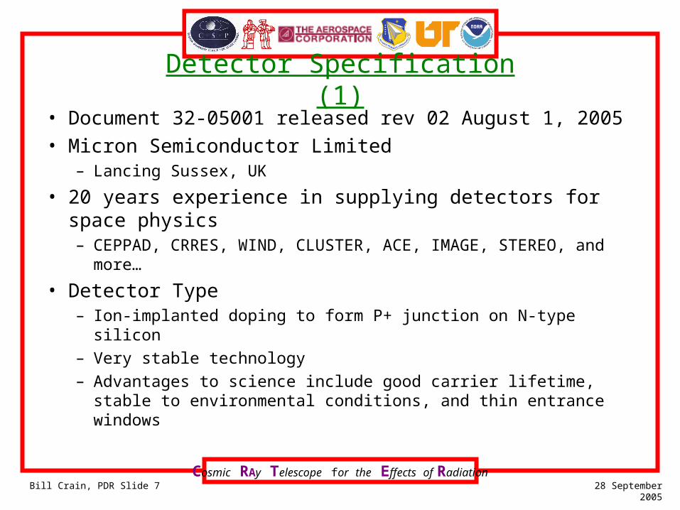
Detector Specification (1)
• Document 32-05001 released rev 02 August 1, 2005
• Micron Semiconductor Limited– Lancing Sussex, UK
• 20 years experience in supplying detectors for space physics– CEPPAD, CRRES, WIND, CLUSTER, ACE, IMAGE, STEREO,
and more…
• Detector Type– Ion-implanted doping to form P+ junction on N-type silicon
– Very stable technology
– Advantages to science include good carrier lifetime, stable to environmental conditions, and thin entrance windows
Cosmic RAy Telescope for the Effects of RadiationBill Crain, PDR Slide 8 28 September 2005
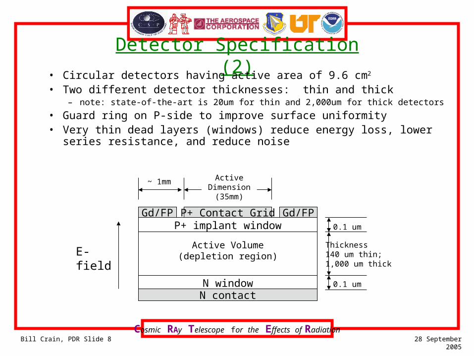
Detector Specification (2)• Circular detectors having active area of 9.6 cm2
• Two different detector thicknesses: thin and thick– note: state-of-the-art is 20um for thin and 2,000um for thick detectors
• Guard ring on P-side to improve surface uniformity• Very thin dead layers (windows) reduce energy loss, lower series resistance, and
reduce noise
Gd/FP P+ Contact Grid Gd/FP
Active Volume(depletion region)
P+ implant window
N window
0.1 um
0.1 um
Thickness140 um thin;1,000 um thick
Active Dimension
(35mm)
N contact
E-field
~ 1mm
Cosmic RAy Telescope for the Effects of RadiationBill Crain, PDR Slide 9 28 September 2005
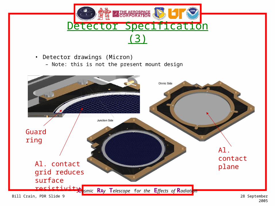
Detector Specification (3)
• Detector drawings (Micron)– Note: this is not the present mount design
Guard ring
Al. contact grid reduces surface resistivity
Al. contact plane
Cosmic RAy Telescope for the Effects of RadiationBill Crain, PDR Slide 10 28 September 2005
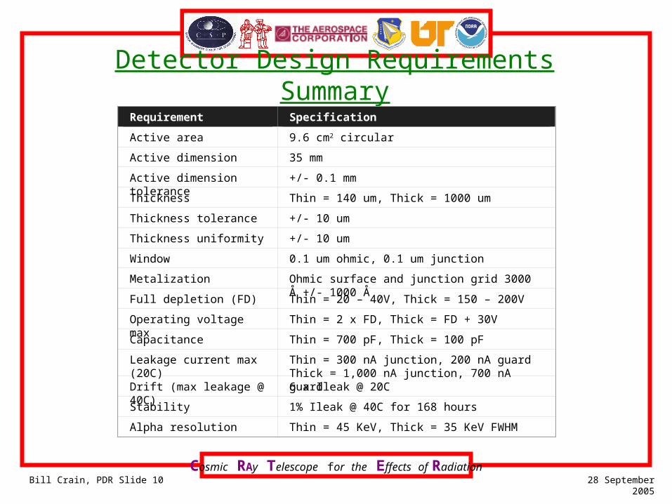
Detector Design Requirements Summary
Requirement Specification
Active area 9.6 cm2 circular
Active dimension 35 mm
Active dimension tolerance +/- 0.1 mm
Thickness Thin = 140 um, Thick = 1000 um
Thickness tolerance +/- 10 um
Thickness uniformity +/- 10 um
Window 0.1 um ohmic, 0.1 um junction
Metalization Ohmic surface and junction grid 3000 Å +/- 1000 Å
Full depletion (FD) Thin = 20 – 40V, Thick = 150 – 200V
Operating voltage max Thin = 2 x FD, Thick = FD + 30V
Capacitance Thin = 700 pF, Thick = 100 pF
Leakage current max (20C)
Thin = 300 nA junction, 200 nA guardThick = 1,000 nA junction, 700 nA guard
Drift (max leakage @ 40C) 6 x Ileak @ 20C
Stability 1% Ileak @ 40C for 168 hours
Alpha resolution Thin = 45 KeV, Thick = 35 KeV FWHM
Cosmic RAy Telescope for the Effects of RadiationBill Crain, PDR Slide 11 28 September 2005
Detector Specification (4)• ISO9001
– Full traceability and serialization
– Travelers maintained
• Qualification tests prior to flight detector shipment– Bond pull test
– Random vibration test
– Thermal cycling
– Stability
• Verification matrix specifies test criteria– Leakage current
– Capacitance
– I-V characteristic
– Alpha resolution / pulser noise measurement
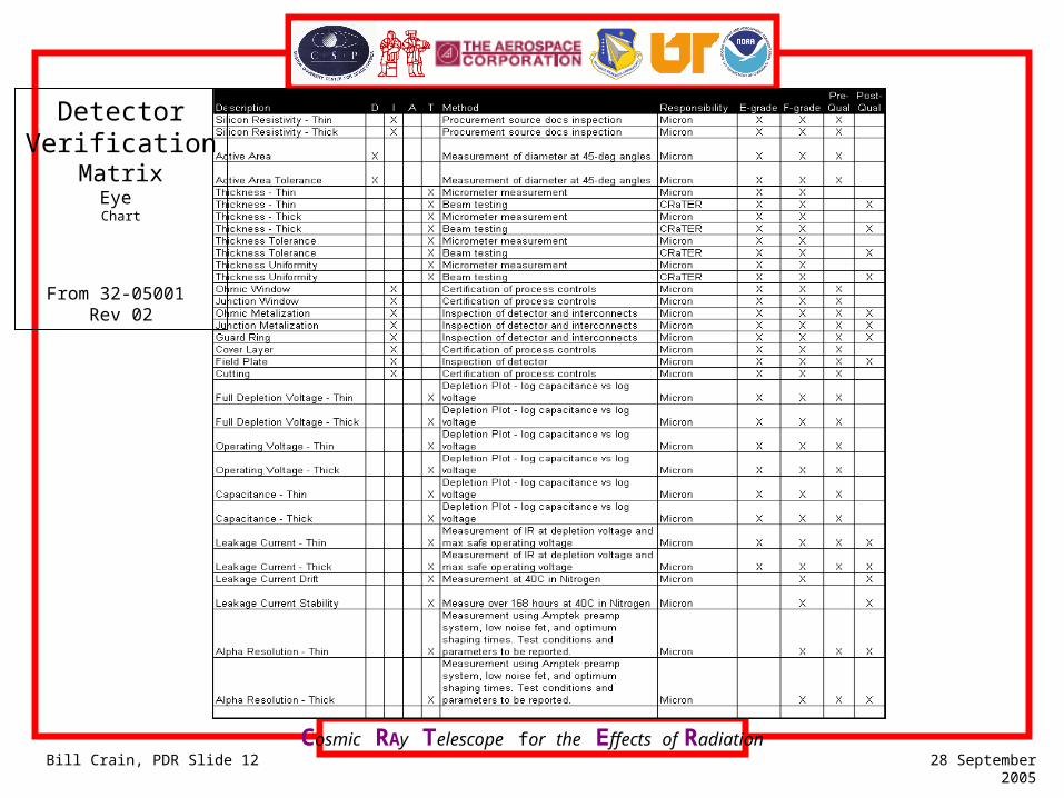
Cosmic RAy Telescope for the Effects of RadiationBill Crain, PDR Slide 12 28 September 2005
DetectorVerification
MatrixEye Chart
From 32-05001 Rev 02
Cosmic RAy Telescope for the Effects of RadiationBill Crain, PDR Slide 13 28 September 2005
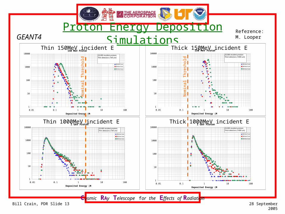
Proton Energy Deposition Simulations Reference:M. Looper
Thin 150MeV incident E Thick 150MeV incident E
Thin 1000MeV incident E Thick 1000MeV incident E1 GeV Protons
1
10
100
1000
10000
0.01 0.1 1 10 100
Deposited Energy (MeV)
Events
Detector 2
Detector 4
Detector 5
20,000 incident protonsThick detectors (1000 um)
1 GeV Protons
1
10
100
1000
10000
0.01 0.1 1 10 100
Deposited Energy (MeV)
Events
Detector 1
Detector 3
Detector 6
20,000 incident protonsThin detectors (140 um)
150 MeV Protons
1
10
100
1000
10000
0.01 0.1 1 10 100
Deposited Energy (MeV)
Events
Detector 2
Detector 4
Detector 5
20,000 incident protonsThick detectors (1000 um)
150 MeV Protons
1
10
100
1000
10000
0.01 0.1 1 10 100
Deposited Energy (MeV)
Events
Detector 1
Detector 3
Detector 6
20,000 incident protonsThin detectors (140 um)
Nom
inal
Thr
esho
ld
Nom
inal
Thr
esho
ld
GEANT4
Cosmic RAy Telescope for the Effects of RadiationBill Crain, PDR Slide 14 28 September 2005
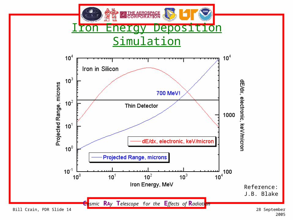
Iron Energy Deposition Simulation
Reference:J.B. Blake
Cosmic RAy Telescope for the Effects of RadiationBill Crain, PDR Slide 15 28 September 2005
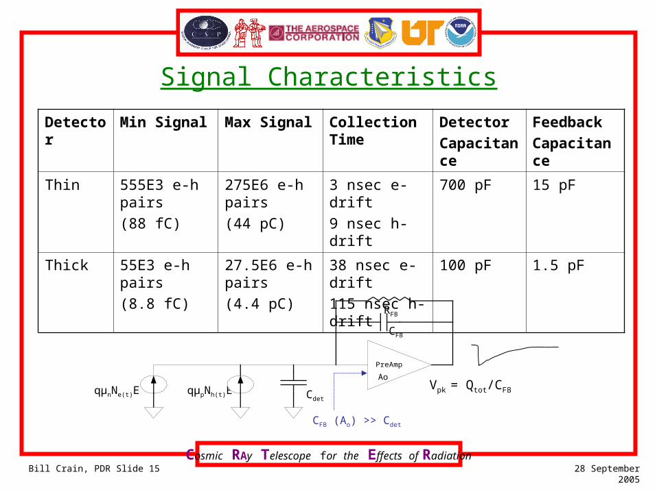
Signal Characteristics
Detector Min Signal Max Signal Collection Time
Detector
Capacitance
Feedback
Capacitance
Thin 555E3 e-h pairs
(88 fC)
275E6 e-h pairs
(44 pC)
3 nsec e-drift
9 nsec h-drift
700 pF 15 pF
Thick 55E3 e-h pairs
(8.8 fC)
27.5E6 e-h pairs
(4.4 pC)
38 nsec e-drift
115 nsec h-drift
100 pF 1.5 pF
qμnNe(t)E qμpNh(t)E
PreAmp
Cdet
CFB
RFB
CFB (Ao) >> Cdet
AoVpk = Qtot/CFB
Cosmic RAy Telescope for the Effects of RadiationBill Crain, PDR Slide 16 28 September 2005
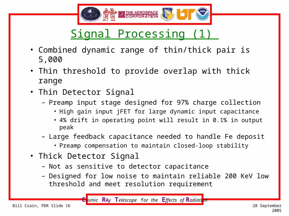
Signal Processing (1)
• Combined dynamic range of thin/thick pair is 5,000
• Thin threshold to provide overlap with thick range
• Thin Detector Signal– Preamp input stage designed for 97% charge collection
• High gain input jFET for large dynamic input capacitance
• 4% drift in operating point will result in 0.1% in output peak
– Large feedback capacitance needed to handle Fe deposit• Preamp compensation to maintain closed-loop stability
• Thick Detector Signal– Not as sensitive to detector capacitance
– Designed for low noise to maintain reliable 200 KeV low threshold and meet resolution requirement
Cosmic RAy Telescope for the Effects of RadiationBill Crain, PDR Slide 17 28 September 2005
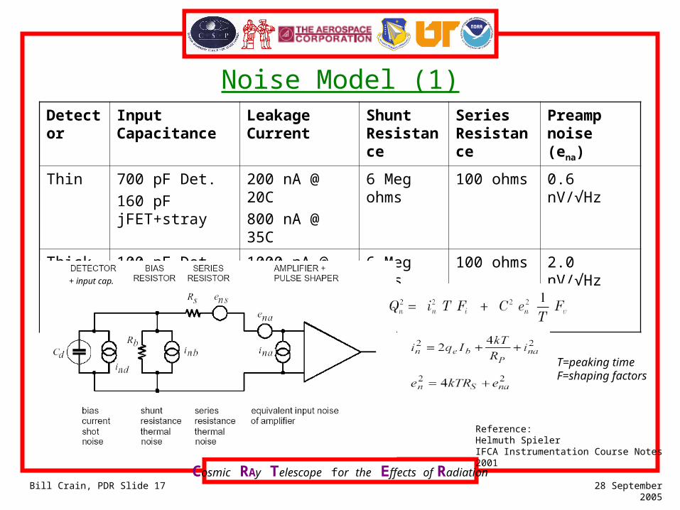
Noise Model (1)
Reference:Helmuth SpielerIFCA Instrumentation Course Notes2001
Detector Input Capacitance
Leakage Current
Shunt Resistance
Series Resistance
Preamp noise (ena)
Thin 700 pF Det.
160 pF jFET+stray
200 nA @ 20C
800 nA @ 35C
6 Meg ohms 100 ohms 0.6 nV/√Hz
Thick 100 pF Det
10 pF jFET+stray
1000 nA @ 20C
4000 nA @ 35C
6 Meg ohms 100 ohms 2.0 nV/√Hz
+ input cap.
T=peaking timeF=shaping factors
Cosmic RAy Telescope for the Effects of RadiationBill Crain, PDR Slide 18 28 September 2005
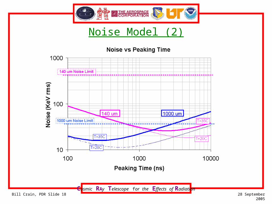
Noise Model (2)
Cosmic RAy Telescope for the Effects of RadiationBill Crain, PDR Slide 19 28 September 2005
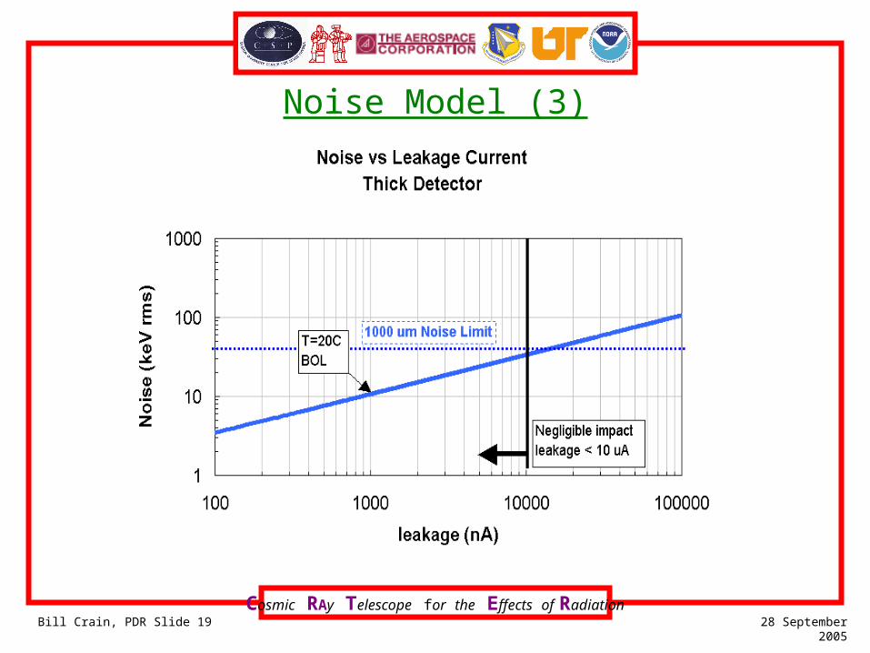
Noise Model (3)
20C BOL
Cosmic RAy Telescope for the Effects of RadiationBill Crain, PDR Slide 20 28 September 2005
Signal Processing (2)
• Noise dominated by thick detector leakage current
• Shaping time same for both thin and thick detectors – ~1 usec for comfortable PHA input timing
– 3-pole gaussian shaping improves symmetry
– 2-complex poles shortens tail
• Coincidence Timing– Noise occupancy in 1-usec coincidence window < 0.1%
– Threshold to noise ratio (T/N) ~ 3.2 for timing discriminator
– Timing discriminator threshold ~ 130 keV• Anticipated BOL T/N ratio is ~ 10
• Allows margin for leakage current drift up to 10 uA
Cosmic RAy Telescope for the Effects of RadiationBill Crain, PDR Slide 21 28 September 2005
Signal Processing (3)
• Other factors affecting noise performance– Bias resistor on thin detector sized to minimize voltage drop
– Bias resistor on thick detector sized to minimize noise
– Detector shot noise doubles every 8 C• Beneficial to operate cold; preferably below 20 C
Cosmic RAy Telescope for the Effects of RadiationBill Crain, PDR Slide 22 28 September 2005
Signal Processing (4)
• Pileup is rare due to low event rate and relatively short shaping time– Exception: occasional periods of high ESP flux
• Coincidence timing uncertainty from leading edge trigger is small– Amplified timing discriminator reduces time walk to acceptable
10% uncertainty
• Ballistic deficit is not an issue due to short collection times relative to peaking time of shaper
• Output voltage scaled for PHA input specifications
Cosmic RAy Telescope for the Effects of RadiationBill Crain, PDR Slide 23 28 September 2005
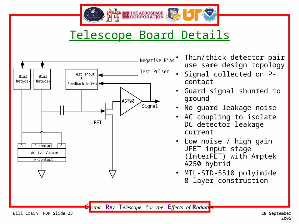
Telescope Board Details
• Thin/thick detector pair use same design topology
• Signal collected on P-contact• Guard signal shunted to
ground• No guard leakage noise• AC coupling to isolate DC
detector leakage current• Low noise / high gain JFET
input stage (InterFET) with Amptek A250 hybrid
• MIL-STD-5510 polyimide 8-layer construction
BiasNetwork
Test Input&
Feedback Network
Negative Bias
Test Pulser
Signal
P-contactG G
N-contact
Active Volume
JFET
BiasNetwork
A250
Cosmic RAy Telescope for the Effects of RadiationBill Crain, PDR Slide 24 28 September 2005
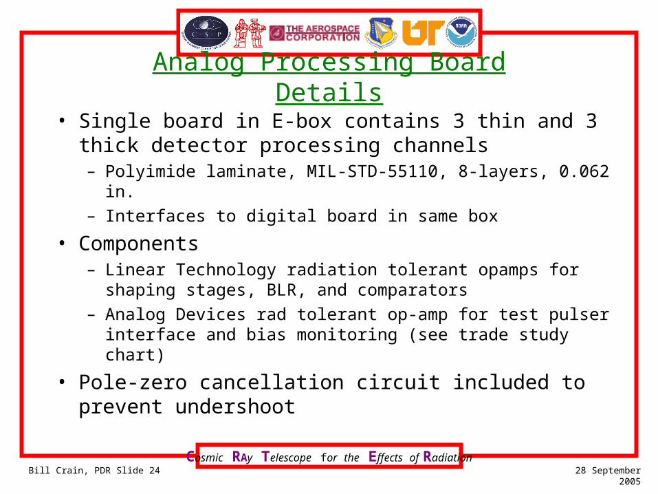
Analog Processing Board Details
• Single board in E-box contains 3 thin and 3 thick detector processing channels– Polyimide laminate, MIL-STD-55110, 8-layers, 0.062 in.
– Interfaces to digital board in same box
• Components– Linear Technology radiation tolerant opamps for shaping stages,
BLR, and comparators
– Analog Devices rad tolerant op-amp for test pulser interface and bias monitoring (see trade study chart)
• Pole-zero cancellation circuit included to prevent undershoot
Cosmic RAy Telescope for the Effects of RadiationBill Crain, PDR Slide 25 28 September 2005
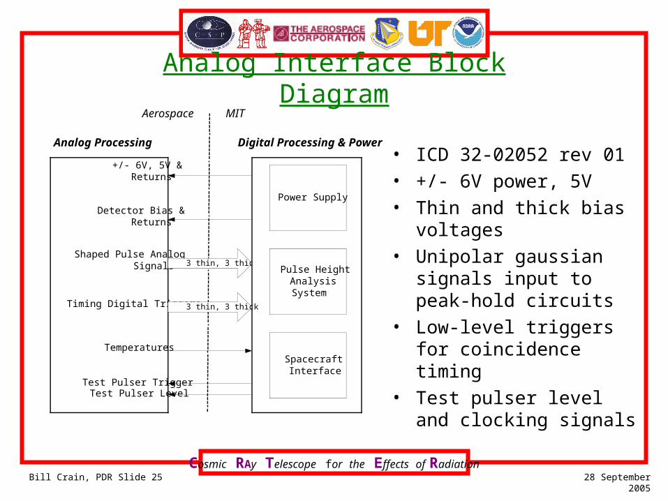
Analog Interface Block Diagram
• ICD 32-02052 rev 01
• +/- 6V power, 5V
• Thin and thick bias voltages
• Unipolar gaussian signals input to peak-hold circuits
• Low-level triggers for coincidence timing
• Test pulser level and clocking signals
+/- 6V, 5V &Returns
Shaped Pulse AnalogSignals
Timing Digital Triggers
Test Pulser Level
Detector Bias &Returns
Temperatures
MIT
Test Pulser Trigger
3 thin, 3 thick
Analog Processing
Aerospace
Digital Processing & Power
3 thin, 3 thick
Power Supply
Pulse HeightAnalysisSystem
SpacecraftInterface
Cosmic RAy Telescope for the Effects of RadiationBill Crain, PDR Slide 26 28 September 2005
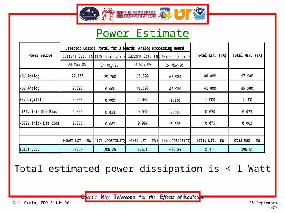
Power Estimate
Current Est. (mA) 10% Uncertainty Current Est. (mA) 10% Uncertainty
24-May-05 24-May-05 24-May-05 24-May-05
+6V Analog 27.000 29.700 61.800 67.980 88.800 97.680
-6V Analog 0.000 0.000 41.800 45.980 41.800 45.980
+5V Digital 0.000 0.000 1.000 1.100 1.000 1.100
-100V Thin Det Bias 0.030 0.033 0.000 0.000 0.030 0.033
-300V Thick Det Bias 0.075 0.083 0.000 0.000 0.075 0.083
Power Est. (mW) 10% Uncertainty Power Est. (mW) 10% Uncertainty Total Est. (mW) Total Max. (mW)
Total Load 187.5 206.25 626.6 689.26 814.1 895.51
Total Est. (mA) Total Max. (mA)
Analog Processing Board
Power Source
Detector Boards (total for 3 boards)
Total estimated power dissipation is < 1 Watt
Cosmic RAy Telescope for the Effects of RadiationBill Crain, PDR Slide 27 28 September 2005
Trade Studies
• Considering detector bias current monitor– Housekeeping item to provide leakage current for each detector
– No impact on noise or failure modes
– Useful for diagnostic purposes especially during environmental testing of flight units
Cosmic RAy Telescope for the Effects of RadiationBill Crain, PDR Slide 28 28 September 2005
Summary
• Detectors are well-established technology from experienced supplier
• Detector specification and Analog/Digital ICD documents have been released
• Electronics design meets requirements of instrument requirements document 32-01205
Cosmic RAy Telescope for the Effects of RadiationBill Crain, PDR Slide 29 28 September 2005