Embed Size (px)
Citation preview
Detection of Boron Segregation to Grain Boundaries in Silicon Carbideby Spatially Resolved Electron Energy-Loss Spectroscopy
Hui Gu and Yutaka Shinoda
‘‘Ceramics Superplasticity’’ International Cooperative Research Project (ICORP),Japan Science and Technology Corporation, Nagoya 456–8587, Japan
Fumihiro Wakai*
Center for Materials Design, Materials and Structures Laboratory, Tokyo Institute of Technology,Yokohama 226-8503, Japan
Boron segregation to grain boundaries in SiC was directlyobserved for the first time by using spatially resolved elec-tron energy-loss spectroscopy methods. The hot-pressed,fully dense material was doped with 0.3 wt% of boron andwas free of other additives, except for 2 wt% of free carbon.The detection of boron was achieved in the difference spec-tra at all the grain boundaries that were examined. Itsinterfacial excess was in the range of 15–29 atoms/nm2, orapproximately one monolayer. Concurrently, silicon deple-tion occurred at these boundaries, although to a lesser ex-tent (−13.5 atoms/nm2 on average), which indicated thatboron mainly replaces silicon and bonds with carbon at thegrain boundary. These findings validate the dual role ofboron at the grain boundary for promoting densificationvia improved grain-boundary diffusivity while maintaininga covalent grain boundary without an oxide phase.
I. Introduction
SINCE the first success to sinter SiC with boron and carbonadditions in the 1970s, the location of the boron and its role
in the sintering process have been of constant interest in SiCresearch. Boron doping is essential to promote densificationand reduce the sintering temperature of SiC ceramics. The firstthermodynamic reason that was proposed for this phenomenonwas that boron decreases the grain-boundary energy.1 Later,more studies were concentrated on the kinetic role of boron insintering: Greskovich and Rosolowski2 proposed that the pres-ence of boron impeded materials transport via surface diffusionand, thus, minimized grain coarsening; on the other hand, thedensification is promoted by materials transport through aboundary phase that is formed by the additives, as suggested bySuzuki and Hase.3,4 Subsequent mechanical-testing data fromvarious groups supported the kinetic picture; for example, Laneet al.5 found the controlling creep mechanism at both low andhigh temperatures to be grain-boundary sliding. Several micro-structural studies did not unambiguously reveal a proposedgrain-boundary film.6,7 The grain boundary in SiC was thoughtto be an ‘‘extended boundary’’ with a reconstructed boron-freecrystalline-like structure8,9 instead of disordered secondary-phase films that were filled with additives. Recent observationsclearly revealed amorphous films in samples that were codopedwith aluminum.10–12 The key to solve the controversy lies inthe true role of boron in the grain boundary.
Unlike aluminum, boron segregation to the grain boundaryhas never been clearly detected.5–9Although some of the blamehas always been placed on the detection limit, many peoplestarted to believe that boron did not segregate to the boundary,relating the infrequently observed amorphous films to othersources. Given the fundamental significance of boron in SiC, itseems worthwhile to attempt to detect boron segregation to thegrain boundary. Recently, analytical tools—especially electronenergy-loss spectroscopy (EELS)—have been very deeply in-volved in grain-boundary analysis, and remarkable progresshas been witnessed in both instrumentation and methodology.In this paper, we report the detection of boron segregationusing EELS analysis in boron- and carbon-doped high-puritySiC for the first time.
II. Experimental Methods
The bulk SiC material was sintered via hot pressing at atemperature of 2000°C for 1 h. The starting materials wereultrafine SiC powders that were 30 nm in size from a commer-cial source (T1 grade, Sumitomo Ohsaka Cement Co., Tokyo,Japan). They contained 1.27 wt% of free carbon and 1.57 wt%of oxygen, which were trapped at the surfaces of the fine pow-ders. Oxygen was determined to have escaped during sinteringat high temperatures, because it was not detected at grainboundaries or triple points, as detailed in the next section. Thecation impurities were all below the 1 ppm level or were evenundetectable. Pure boron (0.3 wt%) was mixed with startingpowders before sintering. The resulted materials were princi-pally b-phase with a trace amount ofa-phase (<5%), as re-vealed via X-ray diffractometry (XRD); stacking faults werefrequently observed via scanning electron microscopy (SEM)and transmission electron microscopy (TEM). The grain sizewas∼2 mm, and the density was 3.15 g/cm3 (or 98.1% of thetheoretical value).
TEM specimens were prepared by using standard slicing andpolishing methods before undergoing argon-ion milling. High-resolution electron microscopy (HREM) observation was per-formed in an electron microscope (Model EM 002B, TopconCorp., Tokyo, Japan) that was operated at 200 kV. The point-to-point resolution of this machine was 1.9 Å. The grain bound-aries were imaged edge-on, as judged from the behavior of theFresnel fringes at various amounts of defocus. However, be-cause most of SiC grain surfaces do not facet, grain-boundaryplanes generally were not flat enough to enable HREM toreveal the local structure near the grain boundaries directly andunambiguously.
The analytical work was performed by using a dedicatedscanning transmission electron microscopy (STEM) micro-scope (Model HB601UX/R2, VG Scientific, East Grinstead,England) that was operated at 100 kV with a field-emissionsource. The energy resolution was 0.5–0.7 eV, and the conver-
L. C. DeJonghe—contributing editor
Manuscript No. 189993. Received July 27, 1998; approved November 16, 1998.*Member, American Ceramic Society.
J. Am. Ceram. Soc., 82 [2] 469–72 (1999)Journal
469
gent and collection semi-angles that were used in this workwere both 12 mrad. The STEM microscope also was fitted witha parallel EELS spectrometer (DigiPEELS, Model 766, Gatan,Pleasanton, CA). A dispersion of 0.5 eV per channel was se-lected to record all the elements simultaneously.
To detect the weak boron signal at the grain-boundary re-gions, all the spectra were recorded in the first difference modeto remove the systematic channel-to-channel gain variation. Toquantify the boron concentration, spectra were taken from ras-tered square areas of a known size (5 nm × 5 nm, including theprobe size and the beam broadening)on andoff the interestedboundaries. The amount of boron segregation was calculated asan interfacial excess, with respect to a bulk constituent such ascarbon:13,14
GB =sB
sCSIB~on!
IC~on!−
IB~off!
IC~off!DNCw (1)
s is the EELS partial cross section of the subscript element;I(on) andI(off) are the signal intensities of the subscript ele-ment in the two scanning boxes, respectively;NC is the sitedensity of carbon in SiC (48.2 atoms/nm3); andw is the widthof the rastered area across the boundary (5 nm). The boronconcentration in SiC is too low to detect; thus,IB(off) 4 0.Equation (1) can also be applied to other elements, such assilicon. In this case, however, the calculated excess is rela-tive to its bulk concentration, and it may be either positive ornegative.
Alternatively, boron detection was also achieved using the‘‘spatial difference’’ method15,16 in the normal spectral mode.The silicon L2,3 edge is sensitive to the bonding change intetrahedrally coordinated silicon.16,17This property can be usedto exclude the matrix signal in the analysis of the grain bound-ary and, thus, obtain the grain-boundary composition and otheruseful parameters.13,18,19
The weak boron signal was quantified through least-squarefitting (Tence, Laboratoire de Physique des Solides, Paris,France20) by using a reference spectrum from the B4C phaseunder the same experimental conditions. The intensities of theother signals (Si and C) were integrated using the standardbackground stripping routine.21
III. Results and Discussions
HREM imaging has shown a grain boundary in this sample(Fig. 1). This is a general boundary without any special relationbetween the two grains. No distinct amorphous film can befound, although it is clear that the boundary is not coherent andthere is a certain degree of structural disorder.
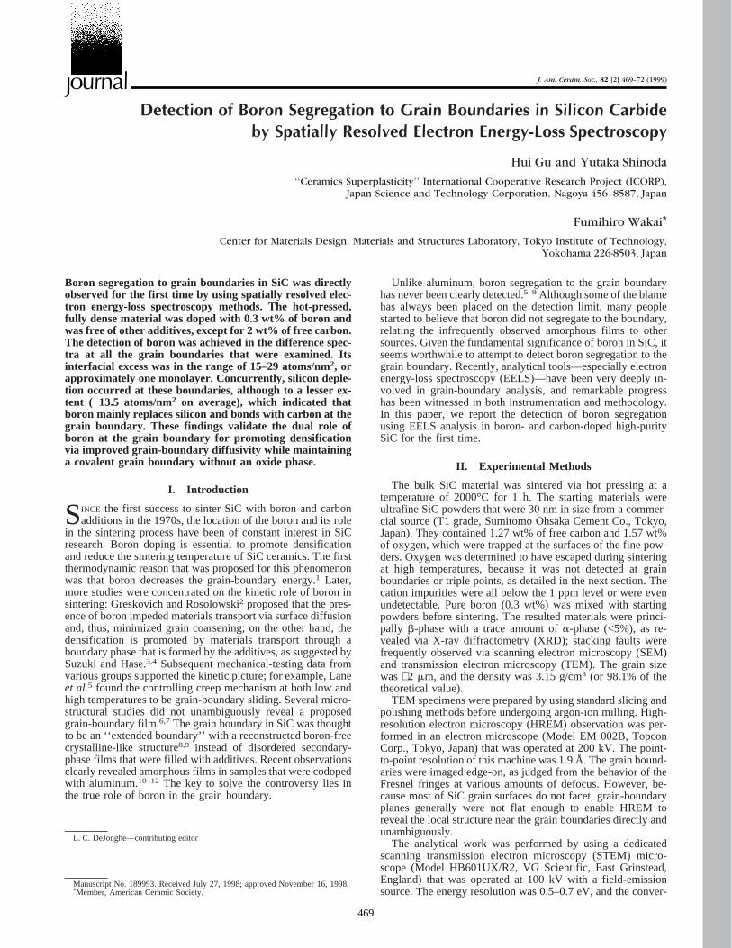
Boron was detected in all ten boundaries that were analyzed.A first-difference spectrum is shown in Fig. 2, together withthose from an SiC grain and the B4C reference. The boronK-edge signal from the boundary overlaps with the extendedstructures of the SiL1 signal; however, compared with the SiCand B4C spectra in the same spectral range, the arrowed peakclearly originates from the boron signal. A barely visible peakat its right side is more evidence for the presence of boron andis an indication that a similarity in the bonding environmentexists between the boron at the grain boundary and that in B4Cphase.
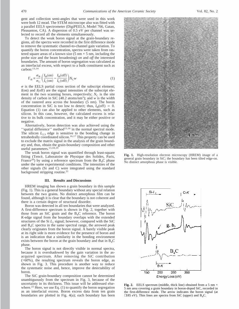
The boron signal is not directly visible in normal spectra,because it is overshadowed by the gain variation in the as-acquired spectrum. After removing the SiC contribution(>60%), the resulting spectrum reveals the boron edge, asshown in Fig. 3. This procedure is another way to reducethe systematic noise and, hence, improve the detectability ofboron.
The SiC grain-boundary composition cannot be determinedunambiguously from the spectrum in Fig. 3, because of theuncertainty in its thickness. This issue will be addressed else-where.22 Here, we use Eq. (1) to quantify the boron segregationas an interfacial excess. Boron excess data from ten grainboundaries are plotted in Fig. 4(a); each boundary has been
Fig. 1. High-resolution electron microscopy (HREM) image of ageneral grain boundary in SiC; the boundary has been tilted edge-on.No distinct amorphous phase is visible.
Fig. 2. EELS spectrum (middle, thick line) obtained from a 5 nm ×5 nm area covering a grain boundary in boron-doped SiC, recorded inthe first-difference mode. The arrow indicates the boron signal (at∼185 eV). Thin lines are spectra from SiC (upper) and B4C.
470 Communications of the American Ceramic Society Vol. 82, No. 2
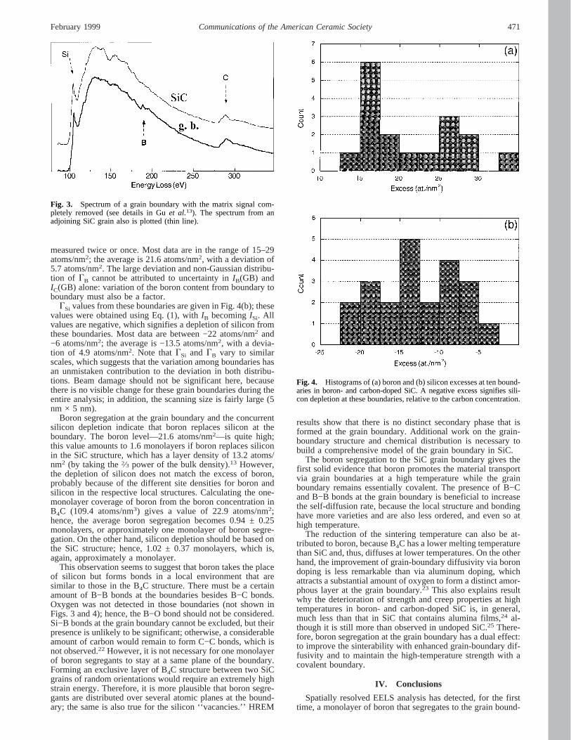
measured twice or once. Most data are in the range of 15–29atoms/nm2; the average is 21.6 atoms/nm2, with a deviation of5.7 atoms/nm2. The large deviation and non-Gaussian distribu-tion of GB cannot be attributed to uncertainty inIB(GB) andIC(GB) alone: variation of the boron content from boundary toboundary must also be a factor.
GSi values from these boundaries are given in Fig. 4(b); thesevalues were obtained using Eq. (1), withIB becomingISi. Allvalues are negative, which signifies a depletion of silicon fromthese boundaries. Most data are between −22 atoms/nm2 and−6 atoms/nm2; the average is −13.5 atoms/nm2, with a devia-tion of 4.9 atoms/nm2. Note thatGSi and GB vary to similarscales, which suggests that the variation among boundaries hasan unmistaken contribution to the deviation in both distribu-tions. Beam damage should not be significant here, becausethere is no visible change for these grain boundaries during theentire analysis; in addition, the scanning size is fairly large (5nm × 5 nm).
Boron segregation at the grain boundary and the concurrentsilicon depletion indicate that boron replaces silicon at theboundary. The boron level—21.6 atoms/nm2—is quite high;this value amounts to 1.6 monolayers if boron replaces siliconin the SiC structure, which has a layer density of 13.2 atoms/nm2 (by taking the2⁄3 power of the bulk density).13 However,the depletion of silicon does not match the excess of boron,probably because of the different site densities for boron andsilicon in the respective local structures. Calculating the one-monolayer coverage of boron from the boron concentration inB4C (109.4 atoms/nm3) gives a value of 22.9 atoms/nm2;hence, the average boron segregation becomes 0.94 ± 0.25monolayers, or approximately one monolayer of boron segre-gation. On the other hand, silicon depletion should be based onthe SiC structure; hence, 1.02 ± 0.37 monolayers, which is,again, approximately a monolayer.
This observation seems to suggest that boron takes the placeof silicon but forms bonds in a local environment that aresimilar to those in the B4C structure. There must be a certainamount of B−B bonds at the boundaries besides B−C bonds.Oxygen was not detected in those boundaries (not shown inFigs. 3 and 4); hence, the B−O bond should not be considered.Si−B bonds at the grain boundary cannot be excluded, but theirpresence is unlikely to be significant; otherwise, a considerableamount of carbon would remain to form C−C bonds, which isnot observed.22 However, it is not necessary for one monolayerof boron segregants to stay at a same plane of the boundary.Forming an exclusive layer of B4C structure between two SiCgrains of random orientations would require an extremely highstrain energy. Therefore, it is more plausible that boron segre-gants are distributed over several atomic planes at the bound-ary; the same is also true for the silicon ‘‘vacancies.’’ HREM
results show that there is no distinct secondary phase that isformed at the grain boundary. Additional work on the grain-boundary structure and chemical distribution is necessary tobuild a comprehensive model of the grain boundary in SiC.
The boron segregation to the SiC grain boundary gives thefirst solid evidence that boron promotes the material transportvia grain boundaries at a high temperature while the grainboundary remains essentially covalent. The presence of B−Cand B−B bonds at the grain boundary is beneficial to increasethe self-diffusion rate, because the local structure and bondinghave more varieties and are also less ordered, and even so athigh temperature.
The reduction of the sintering temperature can also be at-tributed to boron, because B4C has a lower melting temperaturethan SiC and, thus, diffuses at lower temperatures. On the otherhand, the improvement of grain-boundary diffusivity via borondoping is less remarkable than via aluminum doping, whichattracts a substantial amount of oxygen to form a distinct amor-phous layer at the grain boundary.23 This also explains resultwhy the deterioration of strength and creep properties at hightemperatures in boron- and carbon-doped SiC is, in general,much less than that in SiC that contains alumina films,24 al-though it is still more than observed in undoped SiC.25 There-fore, boron segregation at the grain boundary has a dual effect:to improve the sinterability with enhanced grain-boundary dif-fusivity and to maintain the high-temperature strength with acovalent boundary.
IV. Conclusions
Spatially resolved EELS analysis has detected, for the firsttime, a monolayer of boron that segregates to the grain bound-
Fig. 4. Histograms of (a) boron and (b) silicon excesses at ten bound-aries in boron- and carbon-doped SiC. A negative excess signifies sili-con depletion at these boundaries, relative to the carbon concentration.
Fig. 3. Spectrum of a grain boundary with the matrix signal com-pletely removed (see details in Guet al.13). The spectrum from anadjoining SiC grain also is plotted (thin line).
February 1999 Communications of the American Ceramic Society 471
ary in boron- and carbon-doped SiC. Concurrently, a mono-layer of silicon is depleted, with respect to the carbon content,from the grain boundary. This observation leads to the mainconclusion that boron segregants form covalent bonds withcarbon and also with themselves, which is similar to the case inthe bulk B4C phase. Therefore, the boron improves the grain-boundary diffusivity while retaining the high-tempera-ture strength with essentially covalent bonds at the grainboundary.
Acknowledgments: The authors would like to express their thanks toDr. Guo-Dong Zhan and Dr. Mamoru Mitomo for kindly fabricating the boron-and carbon-doped SiC materials. Beneficial discussions with Dr. Mitomo, Dr.Takayuki Nagano, Dr. Warren J. Moberly Chan, and Prof. S. Tsurekawa are alsoappreciated.
References1S. Prochazka,Special Ceramics 6; pp. 171–82. Edited by P. Popper. British
Ceramic Research Association, Stoke-on-Trent, England, 1975.2C. Greskovich and J. H. Rosolowski, ‘‘Sintering of Covalent Solids,’’J. Am.
Ceram. Soc., 59 [7–8] 336–43 (1976).3T. Hase and H. Suzuki, ‘‘Initial-Stage Sintering ofb-SiC with Concurrent
Boron and Carbon Additions’’ (in Jpn.),Yogyo Kyokaishi, 88 [5] 258–64(1980).
4S. Suzuki and T. Hase, ‘‘Boron Transport and Change of Lattice ParameterDuring Sintering ofb-SiC,’’ J. Am. Ceram. Soc., 63 [5–6] 349–50 (1980).
5J. E. Lane, C. H. Carter Jr., and R. F. Davis, ‘‘Kinetics and Mechanisms ofHigh-Temperature Creep in Silicon Carbide: III, Sintereda-Silicon Carbide,’’J.Am. Ceram. Soc., 71 [4] 281–95 (1988).
6R. Hamminger, G. Grathwhol, and F. Thu¨mmler, ‘‘Microanalytical Inves-tigation of Sintered SiC—Part 2. Study of the Grain Boundaries of Sintered SiCby High Resolution Auger Electron Spectroscopy,’’J. Mater. Sci., 18 [10]3154–60 (1983).
7R. H. J. Hannink, Y. Bando, H. Tanaka, and Y. Inomata, ‘‘MicrostructuralInvestigation and Indentation Response of Pressureless-Sintereda- andb-SiC,’’J. Mater. Sci., 23 [6] 2093–101 (1988).
8Y. Ikuhara, H. Kurishita, and H. Yoshinaga,2nd International Conferenceon Interface in Polymer, Ceramic and Metal Matrix Composites; pp. 673–84.Edited by H. Ishida. Elsevier Science Publishing, New York, 1988.
9S. Tsurekawa, S. Nitta, H. Nakashima, and H. Yoshinaga, ‘‘Grain BoundaryStructures in Silicon Carbide: Verification of the Extended Boundary Concept,’’Interface Sci., 3 [1] 75–84 (1995).
10W. J. Moberly Chan, J. J. Cao, C. J. Gilbert, R. O. Ritchie, and L. C. de
Jonghe, ‘‘The Cubic-to-Hexagonal Transformation to Toughen SiC’’; pp. 177–90 in Ceramic Microstructures ’96.Edited by A. P. Tomsia and A. Glaser.Plenum Press, New York.
11W. J. Moberly Chan, J. J. Cao, and L. C. de Jonghe, ‘‘The Role of Amor-phous Grain Boundaries and theb–a Transformation in Toughening SiC,’’ActaMater., 46 [5] 1625–36 (1998).
12T. Nagano, H. Gu, Y. Shinoda, M. Mitomo, and F. Wakai, ‘‘Tensile Duc-tility of Liquid-Phase Sinteredb-Silicon Carbide at Elevated Temperature’’; pp.1897–902 inProceedings of the Third Pacific Rim International Conference onAdvanced Materials and Processing. Edited by M. A. Imam, R. DeNale, S.Hanada, Z. Zhong, and D. N. Lee. The Minerals, Metals & Materials Society,Warrendale, PA, 1998.
13H. Gu, R. M. Cannon, and M. Ru¨hle, ‘‘Composition and Chemical Widthof Ultrathin Amorphous Films at Grain Boundaries in Silicon Nitride,’’J.Mater. Res., 13 [2] 376–87 (1998).
14H. Gu, X. Pan, R. M. Cannon, and M. Ru¨hle, ‘‘Dopant Distribution inGrain-Boundary Films in Calcia-Doped Silicon Nitride Ceramics,’’J. Am. Ce-ram. Soc., 81 [12] 3125–35 (1998).
15J. Bruley, ‘‘Detection of Nitrogen at {100} Platelets in a Type IaA/BDiamond,’’ Philos. Mag. Lett., 66 [1] 47–56 (1992).
16H. Gu, M. Ceh, S. Stemmer, H. Mu¨llejans, and M. Ru¨hle, ‘‘A QuantitativeApproach for Spatially-Resolved Electron Energy-Loss Spectroscopy of GrainBoundaries and Planar Defects on a Subnanometer Scale,’’Ultramicroscopy, 59[1–4] 215–27 (1995).
17H. Gu, ‘‘Distinguishing Ceramic Interfaces through Their Bonding: A NewApproach’’; in Frontiers of Materials Science and Engineering.Edited by S.Somiya, M. Doyama, R. Roy, and R. P. H. Chang. Elsevier Science, Amster-dam, The Netherlands, in press (1999).
18H. Gu, ‘‘ELNES Separation in Spatially-Resolved Analysis of GrainBoundaries and Interfaces,’’Ultramicroscopy, in press (1999).
19H. Gu, ‘‘Quantification of Interfacial Parameters in Spatially-ResolvedAnalysis Involving ELNES Separation,’’Ultramicroscopy, in press (1999).
20M. Tence, M. Quartuccio, and C. Colliex, ‘‘PEELS Compositional Profil-ing and Mapping at Nanometer Spatial Resolution,’’Ultramicroscopy, 58 [1]42–54 (1995).
21R. Egerton,Electron Energy-Loss Spectroscopy in Electron Microscopes.Plenum Press, New York, 1996.
22H. Gu, ‘‘Local Structure and Chemical Bonding in Silicon Carbide withand without Amorphous Films’’; unpublished work.
23L. S. Sigl and H.-J. Kleebe, ‘‘Core/Rim Structure of Liquid-Phase-SinteredSilicon Carbide,’’J. Am. Ceram. Soc., 76 [3] 773–76 (1993).
24G. Grathwohl, T. Reets, and F. Thummler, ‘‘Creep of Hot-Pressed andSintered SiC with Different Sintering Additives,’’Sci. Ceram., 11, 425–31(1981).
25Y. Shinoda, T. Nagano, and F. Wakai, ‘‘Fabrication of NanograinedSilicon Carbide by Ultrahigh-Pressure Hot Isostatic Pressing,’’J. Am. Ceram.Soc., in press. h
472 Communications of the American Ceramic Society Vol. 82, No. 2


![A Spatially Extended Model for Residential Segregationdownloads.hindawi.com/journals/ddns/2007/048589.pdf · which relies on segregation measures and indexes [6, 12, 13], and the](https://img.pdfslide.us/doc/110x75/6018be50e2d2472738110dff/a-spatially-extended-model-for-residential-which-relies-on-segregation-measures.jpg)