Embed Size (px)
Citation preview
CME 392 Laboratory
Revised Feb. 28, 2013 1
Designing with a Microcontroller - II
Safety: In this lab, voltages are less than 15 volts and this is not normally dangerous to humans. However, you should assemble or modify a circuit when power is disconnected and don’t touch a live circuit if you have a cut or break in the skin. Objective: This lab provides an opportunity to use a Stellaris® microcontroller (MCU) and its interfacing to other external devices. It uses the Stellaris® LM4F120 LaunchPad that has an ARM Cortex M4F (LM4F120H5QR) MCU in it. The lab has two parts. Part I of this lab uses the analog to digital converter (ADC) and pulse width modulation (PWM) to build a color generator. In Part II, the students are to design a microcontroller solution to solve one of several tasks.
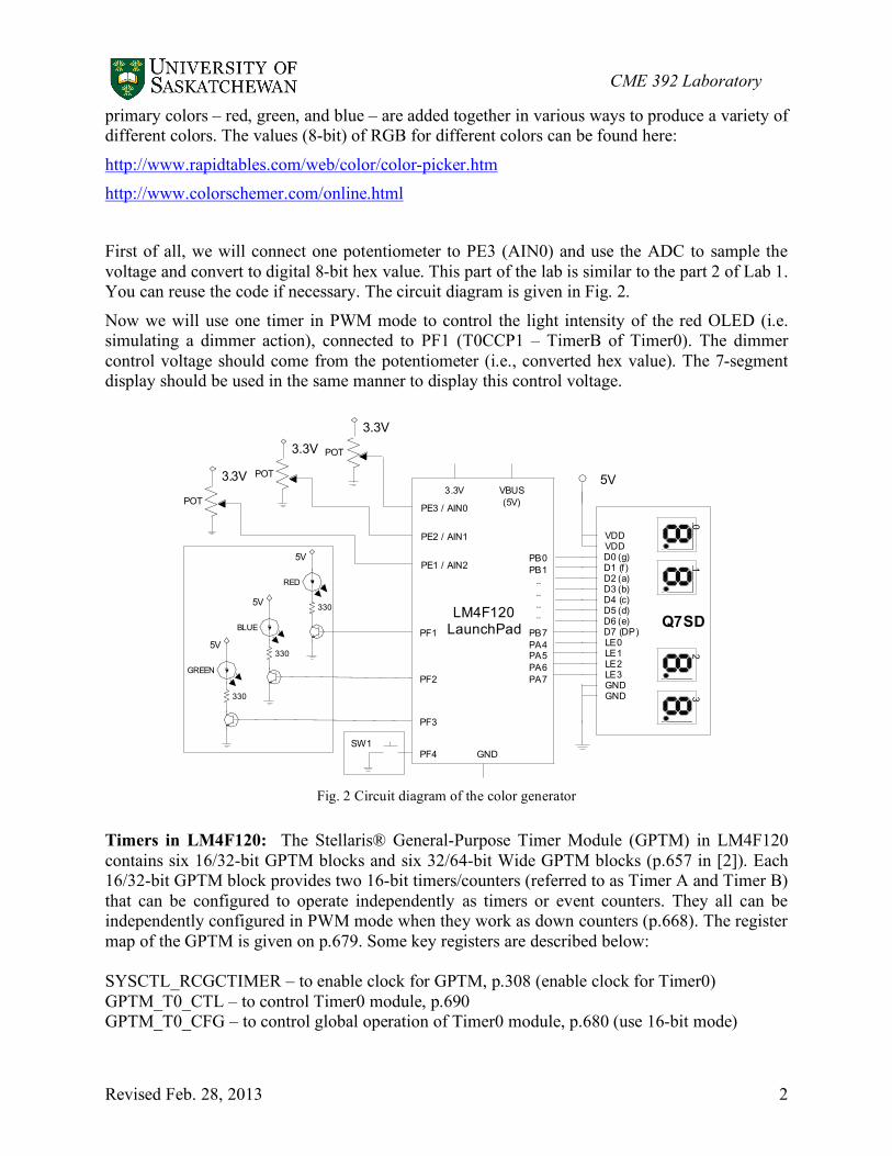
LaunchPad Interface: Before you go to the next section and build your circuit, you should carefully note the pin-out diagram of the LaunchPad. The pin-out diagram of the LaunchPad is shown in Fig. 1. Although the LM4F120H5QR MCU has 43 GPIO, only 35 of them are available through the LaunchPad. They are: 6 pins of Port A (PA2-PA7), 8 pins of Port B (PB0-PB7), 4 pins of Port C (PC4-PC7), 6 pins of Port D (PD0-PD3, PD6-PD7), 6 pins of Port E (PE0-PE5), and 5 pins of Port F (PF0-PF4). In addition, there are two ground, one 3.3V, one 5V (VBUS), and one reset pins available on the LaunchPad. Pins PC0-PC3 are left off as they are used for JTAG debugging. Pins PA0-PA1 are also left off as they are used to create a virtual COM port to connect the LaunchPad to PC. These pins should not be used for regular I/O purpose.
3.3V
PB5
PB0
PB1
PE4
PE5
PB4
PA5
PA6
PA7
VBUS
GND
PD0
PD1
PD2
PD3
PE1
PE2
PE3
PF1
PF2
PF3
PB3
PC4
PC5
PC6
PC7
PD6
PD7
PF4
GND
PB2
PE0
PF0
RST
PB7
PB6
PA4
PA3
PA2
J1 J3 J4 J2
Fig. 1 Header pins on the LaunchPad (EK-LM4F120XL)
Part 1 – Building a color generator The objective is to build a color generator using three pots (of similar rating) and three red, green and blue OLEDs (onboard). The RGB color model is an additive color model in which the
CME 392 Laboratory
Revised Feb. 28, 2013 2
primary colors – red, green, and blue – are added together in various ways to produce a variety of different colors. The values (8-bit) of RGB for different colors can be found here:
http://www.rapidtables.com/web/color/color-picker.htm http://www.colorschemer.com/online.html
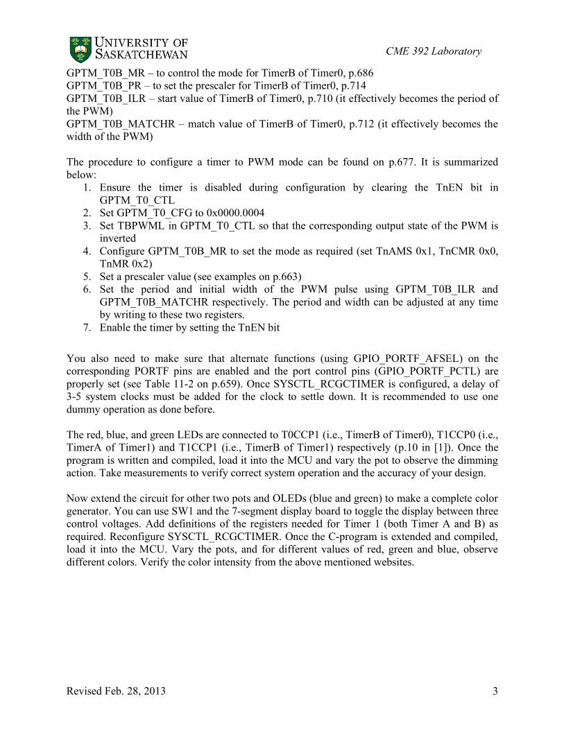
First of all, we will connect one potentiometer to PE3 (AIN0) and use the ADC to sample the voltage and convert to digital 8-bit hex value. This part of the lab is similar to the part 2 of Lab 1. You can reuse the code if necessary. The circuit diagram is given in Fig. 2.
Now we will use one timer in PWM mode to control the light intensity of the red OLED (i.e. simulating a dimmer action), connected to PF1 (T0CCP1 – TimerB of Timer0). The dimmer control voltage should come from the potentiometer (i.e., converted hex value). The 7-segment display should be used in the same manner to display this control voltage.
Q7SD
VDDVDDD0 (g)D1 (f)
LE0LE1LE2LE3GNDGND
01
23
D2 (a)D3 (b)D4 (c)D5 (d)D6 (e)D7 (DP)
LM4F120LaunchPad
PB0PB1
..
..
..
..
PB7PA4PA5PA6PA7
5V
SW1PF4
PE3 / AIN0
GND
3.3V VBUS (5V)
330
RED
5V
PF1
330
BLUE
5V
PF2
330
GREEN
5V
PF3
PE2 / AIN1
PE1 / AIN2
POT
3.3V POT
3.3V POT
3.3V
Fig. 2 Circuit diagram of the color generator
Timers in LM4F120: The Stellaris® General-Purpose Timer Module (GPTM) in LM4F120 contains six 16/32-bit GPTM blocks and six 32/64-bit Wide GPTM blocks (p.657 in [2]). Each 16/32-bit GPTM block provides two 16-bit timers/counters (referred to as Timer A and Timer B) that can be configured to operate independently as timers or event counters. They all can be independently configured in PWM mode when they work as down counters (p.668). The register map of the GPTM is given on p.679. Some key registers are described below: SYSCTL_RCGCTIMER – to enable clock for GPTM, p.308 (enable clock for Timer0) GPTM_T0_CTL – to control Timer0 module, p.690 GPTM_T0_CFG – to control global operation of Timer0 module, p.680 (use 16-bit mode)
CME 392 Laboratory
Revised Feb. 28, 2013 3
GPTM_T0B_MR – to control the mode for TimerB of Timer0, p.686 GPTM_T0B_PR – to set the prescaler for TimerB of Timer0, p.714 GPTM_T0B_ILR – start value of TimerB of Timer0, p.710 (it effectively becomes the period of the PWM) GPTM_T0B_MATCHR – match value of TimerB of Timer0, p.712 (it effectively becomes the width of the PWM) The procedure to configure a timer to PWM mode can be found on p.677. It is summarized below:
1. Ensure the timer is disabled during configuration by clearing the TnEN bit in GPTM_T0_CTL
2. Set GPTM_T0_CFG to 0x0000.0004 3. Set TBPWML in GPTM_T0_CTL so that the corresponding output state of the PWM is
inverted 4. Configure GPTM_T0B_MR to set the mode as required (set TnAMS 0x1, TnCMR 0x0,
TnMR 0x2) 5. Set a prescaler value (see examples on p.663) 6. Set the period and initial width of the PWM pulse using GPTM_T0B_ILR and
GPTM_T0B_MATCHR respectively. The period and width can be adjusted at any time by writing to these two registers.
7. Enable the timer by setting the TnEN bit You also need to make sure that alternate functions (using GPIO_PORTF_AFSEL) on the corresponding PORTF pins are enabled and the port control pins (GPIO_PORTF_PCTL) are properly set (see Table 11-2 on p.659). Once SYSCTL_RCGCTIMER is configured, a delay of 3-5 system clocks must be added for the clock to settle down. It is recommended to use one dummy operation as done before. The red, blue, and green LEDs are connected to T0CCP1 (i.e., TimerB of Timer0), T1CCP0 (i.e., TimerA of Timer1) and T1CCP1 (i.e., TimerB of Timer1) respectively (p.10 in [1]). Once the program is written and compiled, load it into the MCU and vary the pot to observe the dimming action. Take measurements to verify correct system operation and the accuracy of your design. Now extend the circuit for other two pots and OLEDs (blue and green) to make a complete color generator. You can use SW1 and the 7-segment display board to toggle the display between three control voltages. Add definitions of the registers needed for Timer 1 (both Timer A and B) as required. Reconfigure SYSCTL_RCGCTIMER. Once the C-program is extended and compiled, load it into the MCU. Vary the pots, and for different values of red, green and blue, observe different colors. Verify the color intensity from the above mentioned websites.
CME 392 Laboratory
Revised Feb. 28, 2013 4
Part 2: Student’s Own Design
The second part of this experiment allows for more advanced design using a microcontroller and the results of Part I. Students should select one of the following tasks develop their own procedure for completion and verification.
1. Student’s Own Task – Students are encouraged to propose their own experiment. 2. Warning Lamp – This task is to produce a visible warning system for tank pressure.
You are given a voltage developed by a pressure transducer (for this lab, use the potentiometer of Part Ic) and you are to flash a lamp at 0.5 Hz for normal operation, 1 Hz for mild overpressure, 2 Hz for danger and 4 Hz for extreme danger. The duty cycle of the lamp should be 25% in each case. The nominal pressure transducer voltages for each of these cases are 0.5 V, 1.5 V, 2.5 V and 3.5 V. You should select appropriate voltage thresholds for your four cases. Develop a procedure to verify the accuracy.
3. Remote Control – The task is to remotely control the intensity of a lamp in four steps. Hint: You might use PWM or you might control current using two or more output pins. The remote control might be one of the following: USB keyboard, TV remote control, flashlight (laser pointer not recommended), sound control, or any other suitable device. Develop a procedure to assess the range and reliability of your design.
4. Frequency Counter – The task is to measure the frequency of a 0-5 V square wave input signal in the frequency range 100 Hz to 2000 Hz and use the two digit 7-segment display to indicate the frequency. The only requirement on the frequency display is that it be monotonic with input voltage. Develop a procedure to verify system operation and that the measurement is monotonic.
5. Stepper Motor Control – This task is to operate a stepper motor using a microcontroller. Seven 6-wire motors are available for use.
6. UPC Bar Code Reader – This task is to read the first digit of the manufacturer code and display on one 7-segment readout used in Part Ib. Some UPC bar code information can be found here http://www.morovia.com/education/symbology/upc-a.asp
References 1. Stellaris® LM4F120 LaunchPad User Manual (SPMU289A–Revised December 2012):
http://www.ti.com/tool/sw-ek-lm4f120xl 2. LM4F120H5QR Datasheet (Aug 29, 2012): http://www.ti.com/lit/gpn/lm4f120h5qr
3. Helpful resources: http://users.ece.utexas.edu/~valvano/arm/index.htm
CME 392 Laboratory
Revised Feb. 28, 2013 5
Appendix – Stepper Motor Information
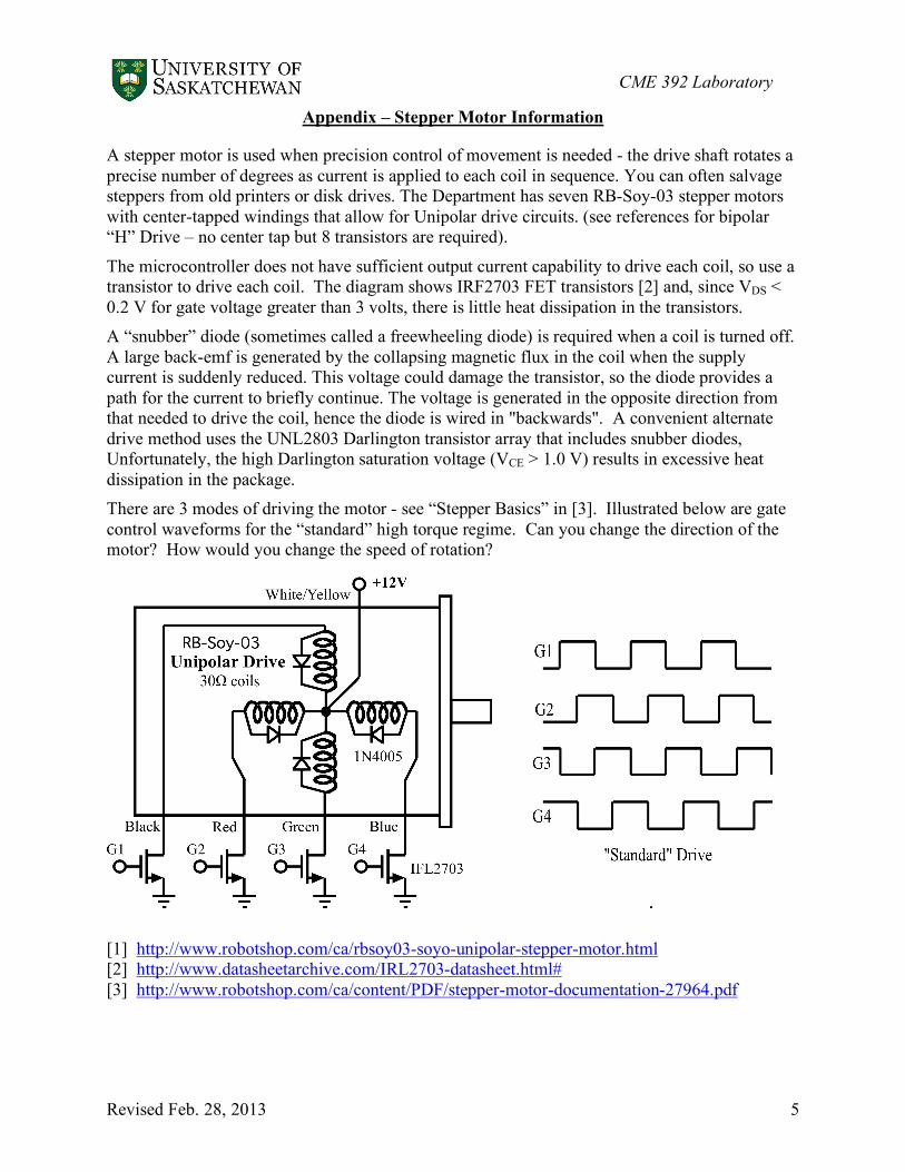
A stepper motor is used when precision control of movement is needed - the drive shaft rotates a precise number of degrees as current is applied to each coil in sequence. You can often salvage steppers from old printers or disk drives. The Department has seven RB-Soy-03 stepper motors with center-tapped windings that allow for Unipolar drive circuits. (see references for bipolar “H” Drive – no center tap but 8 transistors are required).
The microcontroller does not have sufficient output current capability to drive each coil, so use a transistor to drive each coil. The diagram shows IRF2703 FET transistors [2] and, since VDS < 0.2 V for gate voltage greater than 3 volts, there is little heat dissipation in the transistors. A “snubber” diode (sometimes called a freewheeling diode) is required when a coil is turned off. A large back-emf is generated by the collapsing magnetic flux in the coil when the supply current is suddenly reduced. This voltage could damage the transistor, so the diode provides a path for the current to briefly continue. The voltage is generated in the opposite direction from that needed to drive the coil, hence the diode is wired in "backwards". A convenient alternate drive method uses the UNL2803 Darlington transistor array that includes snubber diodes, Unfortunately, the high Darlington saturation voltage (VCE > 1.0 V) results in excessive heat dissipation in the package. There are 3 modes of driving the motor - see “Stepper Basics” in [3]. Illustrated below are gate control waveforms for the “standard” high torque regime. Can you change the direction of the motor? How would you change the speed of rotation?
[1] http://www.robotshop.com/ca/rbsoy03-soyo-unipolar-stepper-motor.html [2] http://www.datasheetarchive.com/IRL2703-datasheet.html# [3] http://www.robotshop.com/ca/content/PDF/stepper-motor-documentation-27964.pdf
CME 392 Laboratory
Revised Feb. 28, 2013 6
Appendix – UPC Bar Code Reader Information
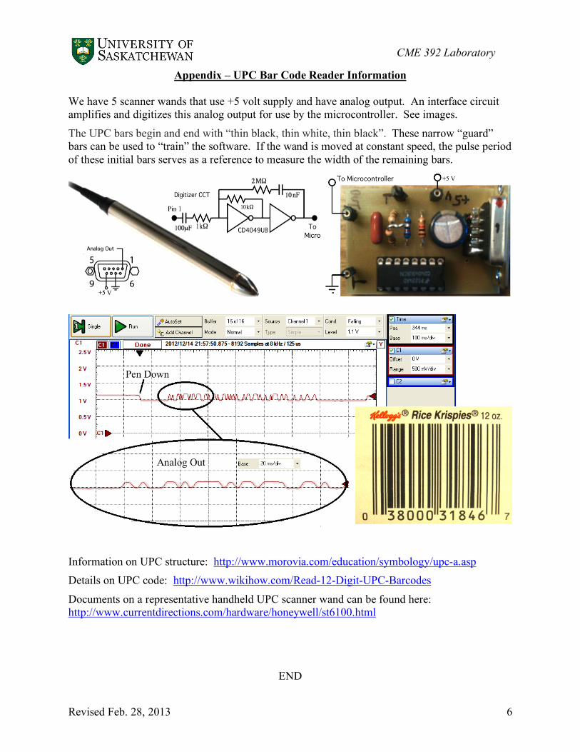
We have 5 scanner wands that use +5 volt supply and have analog output. An interface circuit amplifies and digitizes this analog output for use by the microcontroller. See images.
The UPC bars begin and end with “thin black, thin white, thin black”. These narrow “guard” bars can be used to “train” the software. If the wand is moved at constant speed, the pulse period of these initial bars serves as a reference to measure the width of the remaining bars.
Information on UPC structure: http://www.morovia.com/education/symbology/upc-a.asp Details on UPC code: http://www.wikihow.com/Read-12-Digit-UPC-Barcodes
Documents on a representative handheld UPC scanner wand can be found here: http://www.currentdirections.com/hardware/honeywell/st6100.html
END