Embed Size (px)
Citation preview
Designing for Reuse of Configurable Logic Joseph P. Elm
July 2005
TECHNICAL REPORT CMU/SEI-2005-TR-016 ESC-TR-2005-016

Pittsburgh, PA 15213-3890
Designing for Reuse of Configurable Logic CMU/SEI-2005-TR-016 ESC-TR-2005-016 Joseph P. Elm
July 2005
Acquisition Support Program
Unlimited distribution subject to the copyright.

This work is sponsored by the U.S. Air Force, Electronic Systems Center, GIGSG/KCF. The Software Engineering Institute is a federally funded research and development center sponsored by the U.S. Department of Defense.
Copyright 2005 Carnegie Mellon University.
NO WARRANTY
THIS CARNEGIE MELLON UNIVERSITY AND SOFTWARE ENGINEERING INSTITUTE MATERIAL IS FURNISHED ON AN "AS-IS" BASIS. CARNEGIE MELLON UNIVERSITY MAKES NO WARRANTIES OF ANY KIND, EITHER EXPRESSED OR IMPLIED, AS TO ANY MATTER INCLUDING, BUT NOT LIMITED TO, WARRANTY OF FITNESS FOR PURPOSE OR MERCHANTABILITY, EXCLUSIVITY, OR RESULTS OBTAINED FROM USE OF THE MATERIAL. CARNEGIE MELLON UNIVERSITY DOES NOT MAKE ANY WARRANTY OF ANY KIND WITH RESPECT TO FREEDOM FROM PATENT, TRADEMARK, OR COPYRIGHT INFRINGEMENT.
Use of any trademarks in this report is not intended in any way to infringe on the rights of the trademark holder.
Internal use. Permission to reproduce this document and to prepare derivative works from this document for internal use is granted, provided the copyright and "No Warranty" statements are included with all reproductions and derivative works.
External use. Requests for permission to reproduce this document or prepare derivative works of this document for external and commercial use should be addressed to the SEI Licensing Agent.
This work was created in the performance of Federal Government Contract Number F19628-00-C-0003 with Carnegie Mel-lon University for the operation of the Software Engineering Institute, a federally funded research and development center. The Government of the United States has a royalty-free government-purpose license to use, duplicate, or disclose the work, in whole or in part and in any manner, and to have or permit others to do so, for government purposes pursuant to the copy-right license under the clause at 252.227-7013.
For information about purchasing paper copies of SEI reports, please visit the publications portion of our Web site (http://www.sei.cmu.edu/publications/pubweb.html).
Table of Contents
Executive Summary ................................................................................................ vii
Abstract..................................................................................................................... ix
1 Introduction ....................................................................................................... 1 1.1 PLDs and Firmware Reuse......................................................................... 1 1.2 Evolution of Programmable Logic Devices ................................................. 2 1.3 FPGAs Today.............................................................................................. 3
2 Overview of FPGAs........................................................................................... 5
3 FPGA Application Design Process.................................................................. 9 3.1 Product Specification ................................................................................ 11 3.2 High-Level Design .................................................................................... 11
3.2.1 Hardware Description Languages................................................. 12 3.2.2 Schematic Capture ....................................................................... 13
3.3 Functional Simulation ............................................................................... 13 3.4 Synthesis .................................................................................................. 14 3.5 Operational Simulation ............................................................................. 14 3.6 Place and Route ....................................................................................... 14 3.7 Test and Verification.................................................................................. 15
4 Reuse ............................................................................................................... 17 4.1 Software Reuse ........................................................................................ 17 4.2 Reuse and FPGA Firmware...................................................................... 20 4.3 Black-Box Reuse ...................................................................................... 22 4.4 White-Box Reuse...................................................................................... 24
5 Evaluating Reusability.................................................................................... 27 5.1 Black-Box Reuse ...................................................................................... 27
5.1.1 General Problem Solution............................................................. 28 5.1.2 Good Development Practices ....................................................... 28 5.1.3 Verification Support....................................................................... 28 5.1.4 Complete Documentation ............................................................. 29
CMU/SEI-2005-TR-016 i
5.2 White-Box Reuse ..................................................................................... 30 5.2.1 Good Development Practices....................................................... 30 5.2.2 Test Support ................................................................................. 32 5.2.3 Comprehensive Testing................................................................ 32 5.2.4 Complete Documentation ............................................................. 33
6 Encouraging Reuse and Reusability ............................................................ 35 6.1 Barriers to Reuse ..................................................................................... 35 6.2 Promoting Reuse...................................................................................... 36
6.2.1 In a Development Organization .................................................... 36 6.2.2 In an Acquisition Organization ...................................................... 36
6.3 Promoting Reusability .............................................................................. 37
7 Summary ......................................................................................................... 39
Appendix A FPGA Firmware Reuse for the Software Communication Architecture ..................................................................................... 41
Appendix B OCP Signals..................................................................................... 53
Appendix C Acronyms......................................................................................... 57
References............................................................................................................... 59
ii CMU/SEI-2005-TR-016
List of Figures
Figure 1: Generic FPGA Architecture ...................................................................... 5
Figure 2: Xilinx’s Representation of a Typical CLB.................................................. 6
Figure 3: Xilinx’s Representation of a Typical Configurable I/O Block..................... 7
Figure 4: FPGA Application Design Process and Its Artifacts................................ 10
Figure 5: An Example of FPGA Reuse .................................................................. 18
Figure 6: Reusable FPGA Assets .......................................................................... 22
Figure 7: Macro I/O Registration ........................................................................... 32
Figure 8: Joint Tactical Radio System (JTRS) Joint Program Office SCA ............. 41
Figure 9: OCP-IP’s Representation of Simple OCP Read and Write .................... 43
Figure 10: OCP Interface Represented as a State Diagram ................................... 45
Figure 11: OCP-IP’s Representation of a Typical OCP Profile ................................ 47
Figure 12: OCP Interface for IP Cores .................................................................... 48
Figure 13: OCP Interface for Non-OCP Devices ..................................................... 49
CMU/SEI-2005-TR-016 iii

iv CMU/SEI-2005-TR-016
List of Tables
Table 1: Reuse Example Answers ....................................................................... 19
Table 2: FPGA Asset Reuse................................................................................. 24
Table 3: Basic OCP Dataflow Signals .................................................................. 43
Table 4: OCP Signals from the OCP 2.1 Specification......................................... 53
CMU/SEI-2005-TR-016 v

vi CMU/SEI-2005-TR-016
Executive Summary
Field-programmable gate arrays (FPGAs) are often utilized in systems to address the conflict-ing needs of increased and volatile performance demands and reduced cost and time-to-market. As FPGAs proliferate, the development of software for FPGAs, often referred to as firmware, becomes a larger contributor to the total project cost and schedule, and the effi-ciency of developing this firmware becomes an issue. Reuse of existing firmware compo-nents is one means of maximizing efficiency. With the growing complexity of FPGAs, the development of firmware has evolved to include similarities with the design of complex software subsystems. Designing reusable FPGA firmware components can leverage many of the approaches and techniques used within the software engineering discipline to design re-usable software components.
Understanding the reusability of FPGA firmware assets requires an understanding of the FPGA programming process. FPGA programs are developed using a multistep process whereby the developer first specifies the desired functionality of the resulting product. This specification drives a high-level design, which produces a functional design usually at the register transfer level (RTL), typically using either the Very High Speed Integrated Circuit (VHSIC) Hardware Description Language (VHDL) or Verilog HDL. After the design is cap-tured, it is tested using a simulation to verify the desired functionality. The tested design is then correlated with the architecture of the target FPGA by a “synthesis” process. This proc-ess converts the RTL design into a gate-level design that can be implemented with the re-sources of the FPGA. This synthesized design is again exercised through simulation to re-verify functionality and verify additional performance parameters such as gate loading, tim-ing, and so on. The tested gate-level design is then mapped to the FPGA resources. The im-plementation process results in the assignment of design elements to FPGA hardware ele-ments and interconnection of the design elements within the FPGA. The final design can again be tested using simulation to verify that functionality and timing constraints are met. The final design is then converted to machine code and downloaded to the FPGA.
Reuse of FPGA firmware components involves not only the reuse of the FPGA software, but reuse of the assets produced during the design process. Firmware may be reused in the form of black-box components or white-box components. Black-box reuse is the reuse of existing FPGA firmware without modification. This produces maximum benefit, but places additional burdens on the original developer, who must ensure that the component is sufficiently robust for reuse in multiple applications. White-box reuse is the appropriation and adaptation of existing FPGA firmware components to suit a new application.
The reusability of FPGA firmware components can be evaluated by examining observable characteristics of the component. Examining characteristics such as the general applicability
CMU/SEI-2005-TR-016 vii
of the problem being solved by the component, the structure and organization of the code, the test and verification support for the component, the level of component testing, and the com-ponent documentation provides insights into the quality of the component and its reusability.
Successful reuse requires both the development of components suitable for reuse and the sub-sequent application of these components in new product developments. The development of reusable components can be promoted by the early identification of reusability as a product requirement. Fulfillment of this requirement is further supported by defining the parameters of the intended reuse and providing sufficient time and resources needed to make the compo-nent reusable. Reuse guidelines for development and documentation are also helpful.
Promoting the reuse of existing components in new applications may be encouraged through contracting actions and requirements development.
viii CMU/SEI-2005-TR-016
Abstract
Field-programmable gate arrays (FPGAs) offer electronic systems designers the opportunity to reduce development cost, reduce time-to-market, increase system performance, and im-prove system adaptability. As FPGAs become larger and more complex, the process of de-veloping firmware for them has evolved to include similarities with the design of complex software subsystems. Reuse of FPGA firmware components can further reduce the system development cost and time-to-market, while also providing product quality improvements.
This technical report provides an overview of a generic FPGA firmware design process and identifies the resulting work products that may be suitable for reuse in future development efforts. It provides a brief summary of research done in the field of software reuse and high-lights its applicability to FPGA firmware. This report also provides guidance to developers on the evaluation of firmware components to determine their suitability for reuse and dis-cusses actions that can be taken by both acquirers and developers to produce reusable FPGA firmware.
CMU/SEI-2005-TR-016 ix

x CMU/SEI-2005-TR-016
1 Introduction
Both technology and market demands are ever-changing; in fact, these two areas are syner-gistic. As technology advances make new products possible, the entry of these products into the marketplace suggests new product possibilities. These possibilities stimulate demand for yet another generation of new products, which then drive development of yet more new tech-nologies. The net result is increasing product complexity, shortened product lifespan, and a need for more rapid incorporation of technology into new product development.
Simultaneously, changing political and economic conditions around the world give rise to demands for reduced time-to-market (or time-to-warfighter) and reduced development costs, creating a need for more rapid and more efficient development cycles.
In summary:
1. We need to produce more complex and more flexible products that incorporate the latest technology.
2. We need to do this in less time, at a lower cost.
These conflicting needs provide the impetus for the use and reuse of programmable logic de-vices (PLDs) and the software that they contain.
1.1 PLDs and Firmware Reuse One strategy to cope with these conflicting needs is the development of “flexible” hardware; hardware that can be easily reconfigured to match the evolving marketplace. The replace-ment of hard-wired logic by PLDs (i.e., hardware elements that can be easily reconfigured) is one element of this strategy. The ability to reconfigure hardware enables some degree of product adaptation as needs and markets change. However, this flexibility is not gained without cost. A new step is added to the design process—PLDs must be programmed to ful-fill their intended functions. Successful PLD development requires effort to be expended in design, implementation, verification, and documentation of this PLD programming, often referred to as firmware. This effort can be both time-consuming and costly. One way to mini-mize this time and cost is to reuse previously developed firmware components.
The economic case in support of firmware reuse is clear [Keating 02]. In the field of applica-tion specific integrated circuit (ASIC) design, a process with similarities to PLD-based de-sign, casual reuse of design code (i.e., the reuse of design code that was not specifically gen-erated for reuse) has been shown to provide a 200% to 300% increase in productivity. While
CMU/SEI-2005-TR-016 1
the design code does not need to be redeveloped for the new application, it does need to be understood, possibly modified, integrated, and verified in the new design. A much greater level of productivity improvement may be obtained by the use of design code that was spe-cifically created for reuse; however, this benefit is also not gained without cost. Creating a block of firmware, usually referred to as a macro, specifically intended for reuse and includ-ing appropriate levels of verification, documentation, and support, may cost 10 times as much as the creation of a single-use macro. For this reason, reusable macros are seldom designed as an integral part of a PLD application development. The application design teams are fo-cused on achieving their immediate project goals and do not have the time or resources needed to develop reusable macros that offer benefits primarily to future programs. As such, macros specifically intended for reuse are often designed by the PLD supplier or third-party vendors. The creation of reusable firmware components is further complicated by the accel-erating pace of both hardware evolution and design tool evolution. Rapid changes in the tar-get hardware and the supporting tools create a short product life for some reusable firmware components.
1.2 Evolution of Programmable Logic Devices By definition, a PLD is a programmable electronic component used to build digital circuits. A logic gate has a fixed function that is determined at the time of its manufacture at the semi-conductor foundry. This function is not mutable and remains constant throughout the life of the component. PLDs are different. Their function is not defined at the time of component manufacture, but at the time of application via firmware created by the application designer. Furthermore, PLDs may be modified via reprogramming even after product delivery. As such, PLDs must be viewed as a hardware/software ensemble.
Firmware design has evolved to include similarities with the design of complex software sub-systems. While there are obvious design considerations unique to hardware components, de-signing reusable firmware components can leverage many of the approaches and techniques used within the software engineering discipline to design reusable software components. Due to this similarity, we use the term software interchangeably with firmware throughout this document, except where distinction is needed for clarity.
The earliest PLDs were programmable read-only memories (PROMs). While these devices were intended for the storage of digital data, design engineers discovered that they could also be used to replace combinatorial logic hardware. This offered the advantage of reconfiguring the logic by reprogramming the PROM rather than modifying the circuit board interconnec-tions.
Recognizing the value of a logic device whose function could be defined by the user, semi-conductor manufacturers created programmable logic arrays (PLAs). PLAs are configured as a fixed topography of logic elements (AND, OR, and NOT gates) with one-time programmable interconnections. These devices are capable of much faster operation than PROMs.
2 CMU/SEI-2005-TR-016
Programmable array logic (PAL) was the next step in the evolution of PLDs. PALs were es-sentially PLAs with the inclusion of sequential logic elements such as flip-flops. Flip-flops are devices capable of responding to input signals by assuming either of two stable states. They are used to store a single bit of information. PALs were later enhanced to include re-programmable interconnections, thus was born gated array logic (GAL). Complex program-mable logic devices (CPLDs) arose as the number and size of PALs or GALs on a single chip increased.
The most recent evolutionary advance in PLDs is the creation of the field-programmable gate array (FPGA). In addition to having somewhat larger capacity, FPGAs differ from CPLDs in that the topography of their logic elements is more versatile, providing more flexibility in their application. An FPGA is an integrated circuit with numerous logic cells that can be viewed as standard components. Each logic cell can be configured to execute a simple logic function that is defined by the developer. The FPGA also contains programmable intercon-nection mechanisms between the logic cells. The term “field programmable” refers to the fact that the FPGA’s function is defined by the developer’s programming at the time of appli-cation, not by the device fabricator at the time of manufacturing. Field programmability al-lows the developer to create complex integrated designs without incurring the high costs as-sociated with building an ASIC.
1.3 FPGAs Today PLDs today find widespread use throughout consumer electronics, industrial electronics, and military electronics. Major suppliers of FPGAs include Xilinx,® Altera,® Actel,® and Quick-Logic.® In addition to providing the FPGAs themselves, many of these suppliers also pro-vide the tools needed to create FPGA-based designs.
As technology continues to evolve, FPGAs get larger and more complex. FPGAs today may have up to 8 million gates, contain 9 megabytes (MB) of memory, run at clock rates over 400 megahertz (MHz), support over 1000 I/O pins, and even include embedded digital signal processors (DSPs), microprocessors, and other “core” elements. This ever-increasing size and complexity is driven both by technology advances and by the demands from designers and users for more features and higher performance. As the size and complexity of the de-vices increase, so does the size and complexity of firmware required to configure them. Much of the development time and effort required for creation of an FPGA-based product lies in the development of this firmware.
As FPGA capabilities have increased, the process of developing FPGA firmware has evolved to exhibit similarities with the design of complex software subsystems. While there are obvi-ous design considerations unique to hardware components, designing reusable FPGA firm-ware components can leverage many of the approaches and techniques used within the soft-ware engineering discipline to design reusable software components.
CMU/SEI-2005-TR-016 3
Configuring an FPGA to perform a designated function can be a complex process. To sup-port this effort, FPGA manufacturers have developed a number of electronic design automa-tion (EDA) tools. Initially, these manufacturer-supplied tools were the only tools available to program FPGAs. However, with the growth of the FPGA market, other third-party suppliers now offer EDA tools with which to perform the FPGA design.
While individual FPGA applications are unique, they may have common features. Many ap-plications perform common functions such as a multiply-and-accumulate function or a binary counter function. Both FPGA manufacturers and third-party sources provide macro libraries of these lower level functions that developers may use in their FPGA applications. These libraries are themselves examples of the power of firmware reuse.
Design tools to assist developers in the application of FPGAs are abundant. FPGA vendors (e.g., Actel, Altera, QuickLogic, Xilinx) provide design tools to support their products. Addi-tionally, third-party vendors (e.g., AccelChip,® Altium,™ Magma® Design Automation, Men-tor Graphics,® Synopsys,® Synplicity®) also provide comprehensive tool sets.
4 CMU/SEI-2005-TR-016
2 Overview of FPGAs
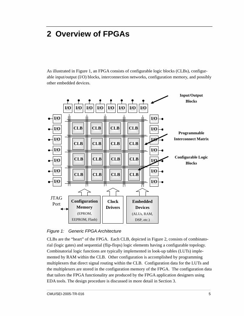
As illustrated in Figure 1, an FPGA consists of configurable logic blocks (CLBs), configur-able input/output (I/O) blocks, interconnection networks, configuration memory, and possibly other embedded devices.
I/O
I/O
I/O
I/O
I/O
I/O
I/O
I/O
I/O
I/O
I/O
I/O
I/O
I/O
I/O I/O I/O I/O I/O I/O I/O I/O
CLB CLB CLB CLB
CLB CLB CLB CLB
CLB CLB CLB CLB
CLB CLB CLB CLB
Input/Output Blocks
Configurable Logic Blocks
Configuration Memory (EPROM,
EEPROM, Flash)
Clock Drivers
Embedded Devices
(ALUs, RAM,
DSP, etc.)
JTAG Port
Programmable Interconnect Matrix
Figure 1: Generic FPGA Architecture
CLBs are the “heart” of the FPGA. Each CLB, depicted in Figure 2, consists of combinato-rial (logic gates) and sequential (flip-flops) logic elements having a configurable topology. Combinatorial logic functions are typically implemented in look-up tables (LUTs) imple-mented by RAM within the CLB. Other configuration is accomplished by programming multiplexers that direct signal routing within the CLB. Configuration data for the LUTs and the multiplexers are stored in the configuration memory of the FPGA. The configuration data that tailors the FPGA functionality are produced by the FPGA application designers using EDA tools. The design procedure is discussed in more detail in Section 3.
CMU/SEI-2005-TR-016 5
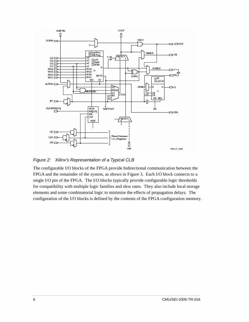
Figure 2: Xilinx’s Representation of a Typical CLB
The configurable I/O blocks of the FPGA provide bidirectional communication between the FPGA and the remainder of the system, as shown in Figure 3. Each I/O block connects to a single I/O pin of the FPGA. The I/O blocks typically provide configurable logic thresholds for compatibility with multiple logic families and slew rates. They also include local storage elements and some combinatorial logic to minimize the effects of propagation delays. The configuration of the I/O blocks is defined by the contents of the FPGA configuration memory.
6 CMU/SEI-2005-TR-016
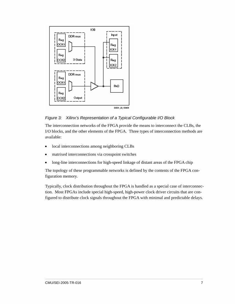
Figure 3: Xilinx’s Representation of a Typical Configurable I/O Block
The interconnection networks of the FPGA provide the means to interconnect the CLBs, the I/O blocks, and the other elements of the FPGA. Three types of interconnection methods are available:
• local interconnections among neighboring CLBs
• matrixed interconnections via crosspoint switches
• long-line interconnections for high-speed linkage of distant areas of the FPGA chip
The topology of these programmable networks is defined by the contents of the FPGA con-figuration memory.
Typically, clock distribution throughout the FPGA is handled as a special case of interconnec-tion. Most FPGAs include special high-speed, high-power clock driver circuits that are con-figured to distribute clock signals throughout the FPGA with minimal and predictable delays.
CMU/SEI-2005-TR-016 7

8 CMU/SEI-2005-TR-016
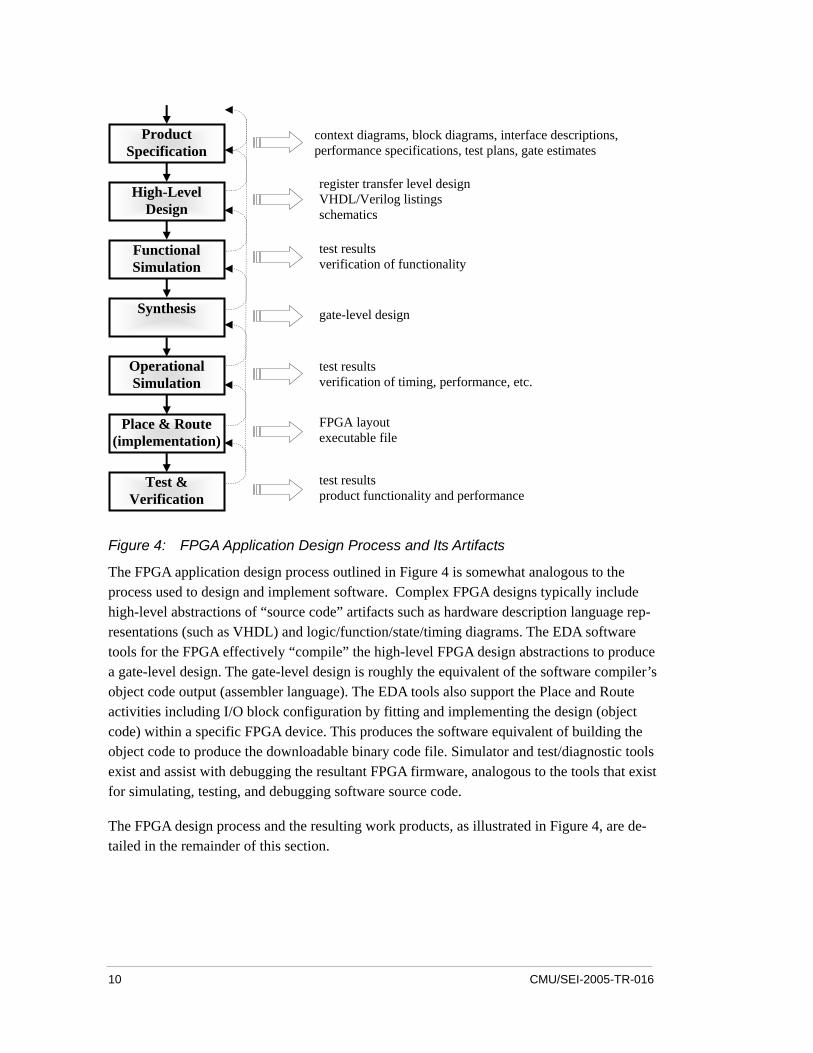
3 FPGA Application Design Process
The process of applying an FPGA to an electronic product is a complex activity requiring performance of multiple tasks and production of intermediate work products. Reusability of FPGA firmware lies in the reusability of these work products. As such, to understand the potential for reuse of FPGA design artifacts, one must first understand the design process used for FPGAs.
FPGAs are best applied within systems using a defined methodology [Zeidman 02]. Al-though many design processes have been promulgated, most embody a core set of tasks, as shown in Figure 4 and described throughout this section. The FPGA design process is sup-ported by a number of EDA tools. These tools enable the developer to define the intended function of the FPGA using schematic diagrams, hardware description languages, or other high-level languages. With the aid of the tool, the developer can then map this design onto the FPGA architecture. Most of these tools also contain simulation capabilities that enable the developer to test the design at various stages prior to download to the FPGA. Finally, the EDA tool can convert the design to the programming language of the FPGA and download it to configure the FPGA to perform the intended function.
A number of artifacts emerge from this design process including the specification, the func-tional model, test plans, test benches, etc. The potential for reuse is in the format and com-pleteness of these artifacts.
CMU/SEI-2005-TR-016 9
Product Specification
High-Level Design
Functional Simulation
Synthesis
Operational Simulation
Place & Route (implementation)
Test & Verification
register transfer level design VHDL/Verilog listings schematics
test results verification of functionality
gate-level design
test results verification of timing, performance, etc.
FPGA layout executable file
test results product functionality and performance
context diagrams, block diagrams, interface descriptions, performance specifications, test plans, gate estimates
Figure 4: FPGA Application Design Process and Its Artifacts
The FPGA application design process outlined in Figure 4 is somewhat analogous to the process used to design and implement software. Complex FPGA designs typically include high-level abstractions of “source code” artifacts such as hardware description language rep-resentations (such as VHDL) and logic/function/state/timing diagrams. The EDA software tools for the FPGA effectively “compile” the high-level FPGA design abstractions to produce a gate-level design. The gate-level design is roughly the equivalent of the software compiler’s object code output (assembler language). The EDA tools also support the Place and Route activities including I/O block configuration by fitting and implementing the design (object code) within a specific FPGA device. This produces the software equivalent of building the object code to produce the downloadable binary code file. Simulator and test/diagnostic tools exist and assist with debugging the resultant FPGA firmware, analogous to the tools that exist for simulating, testing, and debugging software source code.
The FPGA design process and the resulting work products, as illustrated in Figure 4, are de-tailed in the remainder of this section.
10 CMU/SEI-2005-TR-016
3.1 Product Specification The first step in the FPGA application design process is to define the intent and goals of the FPGA application in a detailed specification. In addition to defining the product to be devel-oped, the specification also serves as a primary communication medium not only among the members of the design team, but also among all stakeholders (e.g., users, testers, managers) of the project. The specification typically defines
• Context – This is the environment in which the FPGA will function. This definition of-ten takes the form of an annotated block diagram, showing the FPGA in relation to other system elements.
• Architecture – Internal structure of the design, which describes how the functionality of the design is partitioned and the interfaces between the partitions. It is often in the form of annotated block diagrams, including interface definitions and data flows.
• Input/Output – Definition of the quantity and characteristics of the physical inputs and outputs of the FPGA. This factor is often critical in selecting the specific hardware de-vice appropriate for the application.
• Gate Count Estimates – Rough estimate of the quantity of gates and other resources needed within the FPGA. This factor is often critical in selecting the specific hardware device appropriate for the application.
• Timing Estimates – Rough estimate of the speed and clock rates required for the device.
This factor is often critical in selecting the specific hardware device appropriate for the application.
• Test Plans – Definitions of the functions to be tested, the required results, and the ex-pected test methods. It is important to define testing plans early in the development process to ensure that appropriate hardware resources within the FPGA are dedicated to test support.
Other factors, such as cost, environment, power consumption, packaging, embedded devices, and more may also require definitions within the specification.
After it is completed, the product specification should be distributed to and reviewed by all relevant stakeholders.
3.2 High-Level Design The high-level design specifies the functional design of the FPGA firmware at the register transfer level (RTL).
One of the first design tasks is to select the hardware device. As noted previously, gate count, speed, and I/O capability often play a major role in the selection process. Prior experience of
CMU/SEI-2005-TR-016 11
the design team and the availability of a suitable development environment are also key fac-tors in the selection.
After the hardware device is chosen, high-level design of the firmware can commence. De-vice selection is a significant event for firmware development for several reasons. First, the choice of the FPGA can have a significant impact on the firmware development environment. Many of the development tools are supplied by the FPGA vendors, so the choice of a differ-ent FPGA may result in the use of a different development environment. Second, some FPGAs are better suited for some programming styles rather than others. Many FPGAs and FPGA design tools include design guidelines and recommended coding styles that improve the likelihood of creating a successful design effort with that product.
FPGAs are typically configured in one of the following three ways:
• hardware description language (HDL)
• algorithmic design using other high-level languages
• schematic capture
All of these methods provide a path for capturing the design intent and translating it into the programming necessary for the FPGA to implement that intent.
3.2.1 Hardware Description Languages HDLs provide a means of defining electronic hardware, supporting designs at levels of ab-straction that range from abstract behavioral descriptions down to gate level descriptions. As such, they can be used in both top-down and bottom-up design methodologies. HDLs are not technology-specific, so they can be used with any type of hardware. They support both static and dynamic modeling, enabling them to be used for behavioral analysis (e.g., logic verifica-tion, state verification) and timing verification. While HDLs were initially developed to sup-port integrated circuit designers, they also work well for the specification of FPGA configura-tions. The primary HDLs available today are VHDL and Verilog.
The Very High Speed Integrated Circuit (VHSIC) Hardware Description Language (VHDL) can be used to model a digital system. VHDL is an international standard defined and man-aged by the Institute of Electrical and Electronics Engineers (IEEE) under IEEE-Std-1076-2002 and IEEE-Std-1164-1993.
Verilog 2001 is a general-purpose digital design language supported by multiple verification and synthesis tools. It is an international standard defined and managed by IEEE under IEEE-Std 1364-2001. More recently, SystemVerilog, an enhanced version of Verilog, has been in-troduced by Accellera, an industry association supporting electronic design.
12 CMU/SEI-2005-TR-016
3.2.1.1 Algorithmic Design
A recent development is the use of other high-level languages for the capture of the design intent. Languages such as C and C++ are excellent for behavioral modeling of the design. Several tools capable of converting C/C++ programs into formats suitable for FPGA pro-gramming exist.
MATLAB® is a high-level technical computing language and interactive environment devel-oped and distributed by The MathWorks. It is widely used for system modeling, simulation, and analysis. Compilers that translate MATLAB models into VHDL models suitable for FPGA programming for algorithm development, data visualization, data analysis, and nu-merical computation are available.
Obtaining HDL code from C/C++/MATLAB and other non-HDL languages through the use of translating tools and the automatic generation of HDL code from VHDL models can result in code that is slower or uses more hardware resources than if the original programming was done manually in an HDL. Thus, developers should keep in mind the tradeoffs of developing the FPGA code in this manner.
3.2.2 Schematic Capture Schematic capture is yet another way to design FPGA software. Both FPGA and third-party vendors provide design tools that enable the designer to program the FPGA by generating an electronic schematic. Many designers who come from an electronics background prefer this method, since it emulates the design flow that is most familiar to them. Using the schematic capture tool, much like any other EDA tool, the designer can generate a schematic consisting of gates, registers, and more connected by wires and busses. The schematic capture tool then converts this into a configuration that can be implemented by the CLBs and interconnection structure of the FPGA.
While this design method can be quite efficient for a small design, it is often impractical to produce larger designs in this way due to complexity, high gate count, etc. Also, this method depends heavily on the capabilities of the schematic capture tool. As such, portability of de-signs captured in this way is somewhat limited.
3.3 Functional Simulation Regardless of the tools used, the high-level design process produces an RTL design. The RTL design captures the basic functionality of the application’s design. Before proceeding with more detailed design activities, it is prudent to verify the correctness of this functionality by exercising the RTL model via simulation. Most FPGA design tools support simulation.
To evaluate the performance of the model, the tester creates a test bench, a separate model that generates inputs to and collects outputs from the model under test. With test benches, model performance can be verified by simulating model execution to produce outputs that
CMU/SEI-2005-TR-016 13
can then be compared to the expected outputs. Test benches are often written in HDL, a high-level language such as C++, or a hardware verification language (HVL). It is desirable for the test benches to be developed by someone other than the firmware developer. If the same person or group develops both, then any misunderstanding in the requirements or the intended functionality can appear in both the design and the test bench and thus will not be discovered during the test phase.
Simulation at this level only addresses the functionality of the model. It does not address issues such as signal timing, power consumption, signal loading, and so on.
3.4 Synthesis After the functionality of the design is verified, the next step is to map the design onto the architecture of the FPGA. As shown in Figure 2, the CLBs of the FPGA contain a specific set of logic elements (LUTs, RAM, multiplexers). For example, perhaps the application de-sign calls for a simple logic function such as an 8-input AND gate feeding the J input on a JK flip-flop. These elements are not physically available within the CLB. Instead, the LUTs and multiplexers must be configured to emulate this logic while using the resources of the CLB. Implementation of more complex functions may require resources from many CLBs and sub-stantial exchange of signals between the CLBs. In these cases, the programmable intercon-nect matrix of the FPGA must also be configured to enable the CLBs to share these signals.
The process of converting the application design into a gate-level design that can be imple-mented with the resources of the FPGA is called synthesis. Synthesis is performed by the FPGA design tool. Checking is done at this stage to ensure that basic design rules (for exam-ple, logic fan-in and fan-out) are met and sufficient CLB and interconnect resources are available.
3.5 Operational Simulation We now return to simulation. This round of simulation again verifies the functionality of the design. However, we can now also examine power consumption, gate loading, and timing relationships within the design. If possible, the same test cases used for simulation at the RTL level should also be executed here and identical results should be achieved.
The timing analysis may reveal a need to constrain certain signal paths within the device. These constraints are then addressed during the final phase, placement and routing.
3.6 Place and Route After successfully completing an operational simulation and resolving all timing issues, the next step is to physically map the gate-level design onto the FPGA architecture. This task involves assigning individual design elements to specific CLBs and interconnection mecha-
14 CMU/SEI-2005-TR-016
nisms. Routing software within the FPGA design tool performs this function. Functions hav-ing critical timing constraints are distributed among CLBs in close proximity in order to minimize signal path lengths. The design tool also monitors and controls routing congestion as functions and signal paths are distributed throughout the FPGA.
3.7 Test and Verification The final step in the design process is to download the design into the FPGA and verify that it performs as anticipated. Test cases similar to those run during simulations should be exer-cised and produce equivalent results.
CMU/SEI-2005-TR-016 15

16 CMU/SEI-2005-TR-016
4 Reuse
4.1 Software Reuse A considerable body of research addressing the issue of software reuse exists. Much of this research is equally applicable to firmware reuse. This section discusses the generalities of software reuse, with details of firmware reuse discussed in later sections.
The incentive for reuse of software often arises from
• a desire to reduce cost
• a desire to reduce delivery time
• a desire to improve product quality
Software reuse has the potential to fulfill these needs if done properly. A study of reuse showed a 57% increase in productivity, a 43% decrease in time-to-market, and a 75% de-crease in defect rate [Lim 94]. However, successful reuse requires an initial investment. Be-fore a component can be reused, it must be developed having all of the additional attributes needed to support reuse.
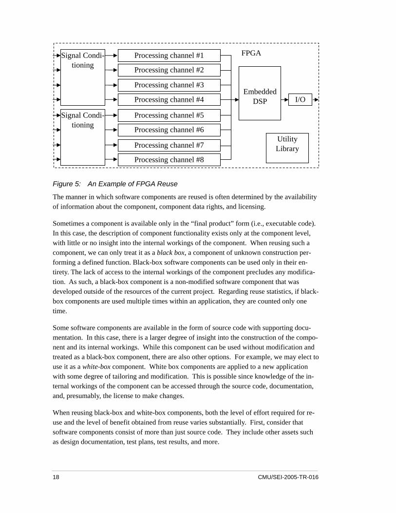
The definition of the term reuse is often not clear and the absence of a firm definition means that it is difficult to accurately determine what many reuse statistics really mean. Consider the FPGA shown in Figure 5, which consists of
• an embedded DSP core
• eight channels of signal processing derived by modifying components from a previous project
• a commercially purchased utility library
• two copies of signal conditioning appropriated from another project
• custom-designed I/O processing
If 90% of the firmware in this FPGA is attributed to reuse, what does this statistic really mean? Is the DSP core counted as reused code? Are seven of the eight signal processing channels counted as reused code? Is the utility library considered reused code? Are both of the signal conditioners instances of reused code? The answer to all of these questions de-pends on how reuse is being defined.
CMU/SEI-2005-TR-016 17
FPGA
Embedded DSP
Processing channel #1
Processing channel #2
Processing channel #3
Processing channel #4
Processing channel #5
Processing channel #6
Processing channel #7
Processing channel #8
Utility Library
Signal Condi-tioning
Signal Condi-tioning
I/O
Figure 5: An Example of FPGA Reuse
The manner in which software components are reused is often determined by the availability of information about the component, component data rights, and licensing.
Sometimes a component is available only in the “final product” form (i.e., executable code). In this case, the description of component functionality exists only at the component level, with little or no insight into the internal workings of the component. When reusing such a component, we can only treat it as a black box, a component of unknown construction per-forming a defined function. Black-box software components can be used only in their en-tirety. The lack of access to the internal workings of the component precludes any modifica-tion. As such, a black-box component is a non-modified software component that was developed outside of the resources of the current project. Regarding reuse statistics, if black-box components are used multiple times within an application, they are counted only one time.
Some software components are available in the form of source code with supporting docu-mentation. In this case, there is a larger degree of insight into the construction of the compo-nent and its internal workings. While this component can be used without modification and treated as a black-box component, there are also other options. For example, we may elect to use it as a white-box component. White box components are applied to a new application with some degree of tailoring and modification. This is possible since knowledge of the in-ternal workings of the component can be accessed through the source code, documentation, and, presumably, the license to make changes.
When reusing black-box and white-box components, both the level of effort required for re-use and the level of benefit obtained from reuse varies substantially. First, consider that software components consist of more than just source code. They include other assets such as design documentation, test plans, test results, and more.
18 CMU/SEI-2005-TR-016
If the reused component is a black-box component, many of these assets remain applicable, though usually unavailable. Reused documentation consists primarily of the component-level descriptions provided with the component. Reused test procedures, test results, and so on consist primarily of built-in test capabilities (if any) embedded in the component.
If the reused component is a white-box component, a greater number of supporting assets may be available. Design documentation, test procedures, and other supporting documents may be provided with the component. However, due to the fact that the white-box compo-nent may be tailored of modified for the application, fewer of these assets are reusable in their original form and may also require tailoring, modification, or even re-creation. One strong advantage of black-box reuse is that the reused components maintain the quality at-tributes embedded in the software as a result of previous verification and application. The tailoring applied to white-box components may compromise these. If software from a prior project or from a prior supplier is modified, many of the benefits of reuse are lost. The soft-ware documentation must also be modified. The software must be retested and reintegrated. The quality benefits arising from the use of “proven” software are lost. This is not to say that the use of modified versions of software assets is not helpful. Indeed, this type of reuse can result in cost savings of 50% of new development costs [Poulin 96]. However, structured reuse of unmodified software assets can produce far better returns.
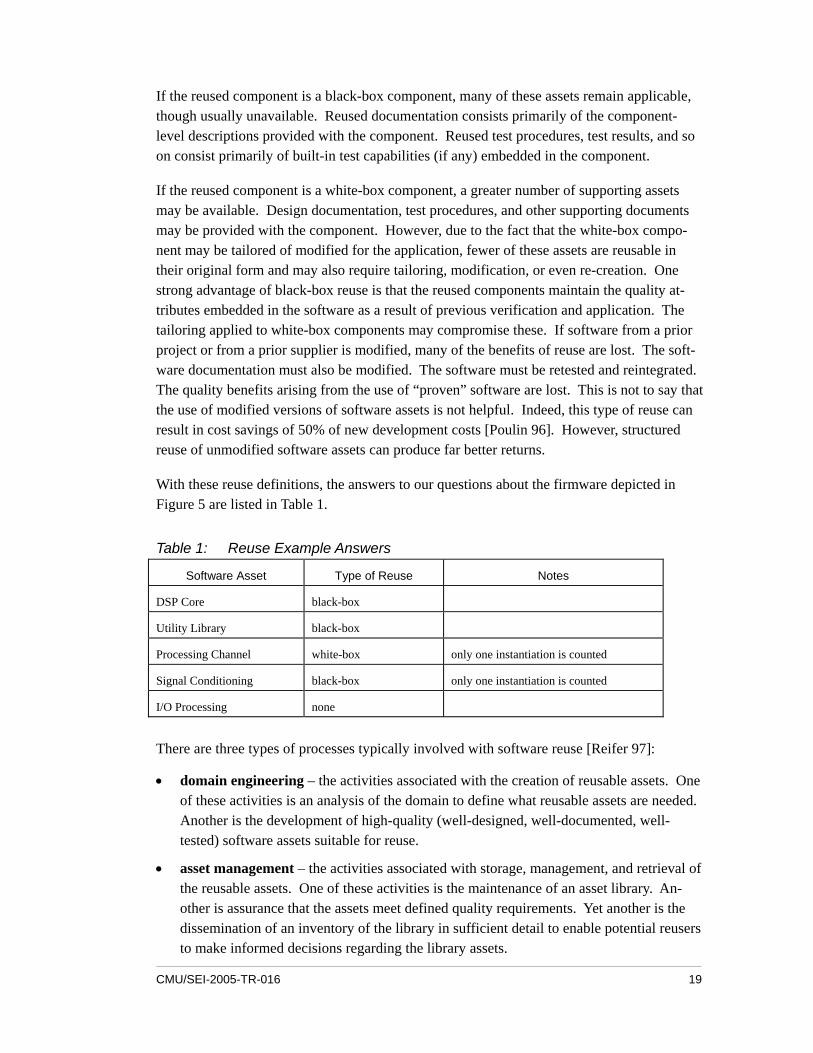
With these reuse definitions, the answers to our questions about the firmware depicted in Figure 5 are listed in Table 1.
Table 1: Reuse Example Answers
Software Asset Type of Reuse Notes
DSP Core black-box
Utility Library black-box
Processing Channel white-box only one instantiation is counted
Signal Conditioning black-box only one instantiation is counted
I/O Processing none
There are three types of processes typically involved with software reuse [Reifer 97]:
• domain engineering – the activities associated with the creation of reusable assets. One of these activities is an analysis of the domain to define what reusable assets are needed. Another is the development of high-quality (well-designed, well-documented, well-tested) software assets suitable for reuse.
• asset management – the activities associated with storage, management, and retrieval of the reusable assets. One of these activities is the maintenance of an asset library. An-other is assurance that the assets meet defined quality requirements. Yet another is the dissemination of an inventory of the library in sufficient detail to enable potential reusers to make informed decisions regarding the library assets.
CMU/SEI-2005-TR-016 19
• application engineering – the activities associated with the application of reusable assets to projects in development. These are the typical design, implementation, test, integra-tion, and documentation activities performed by project engineers.
When most people think of reuse, they envision only cost savings arising from the difference between the cost of new development versus the cost of the application engineering process. They often do not comprehend the costs and time of the domain engineering and asset man-agement processes. When a component is specifically developed with reuse in mind, the de-velopers pay additional attention to the generalization of the solution, clear and complete documentation, and rigorous and comprehensive testing. The costs associated with develop-ment of this type of component may be as much as ten times that of an equivalent single-use component. Alternately, reuse is sometimes attempted as an ad hoc activity; a software asset designed specifically for a prior application is appropriated for a new application. If the software asset has not been designed with reuse in mind, the following problems may arise:
• it may not provide the full functionality needed by the new organization
• it may not have sufficient documentation to enable the developers to properly apply it
• it may not operate correctly
• it may not integrate efficiently with other elements of the new system
In short, it may not provide any net benefits to the developer [Keating 02].
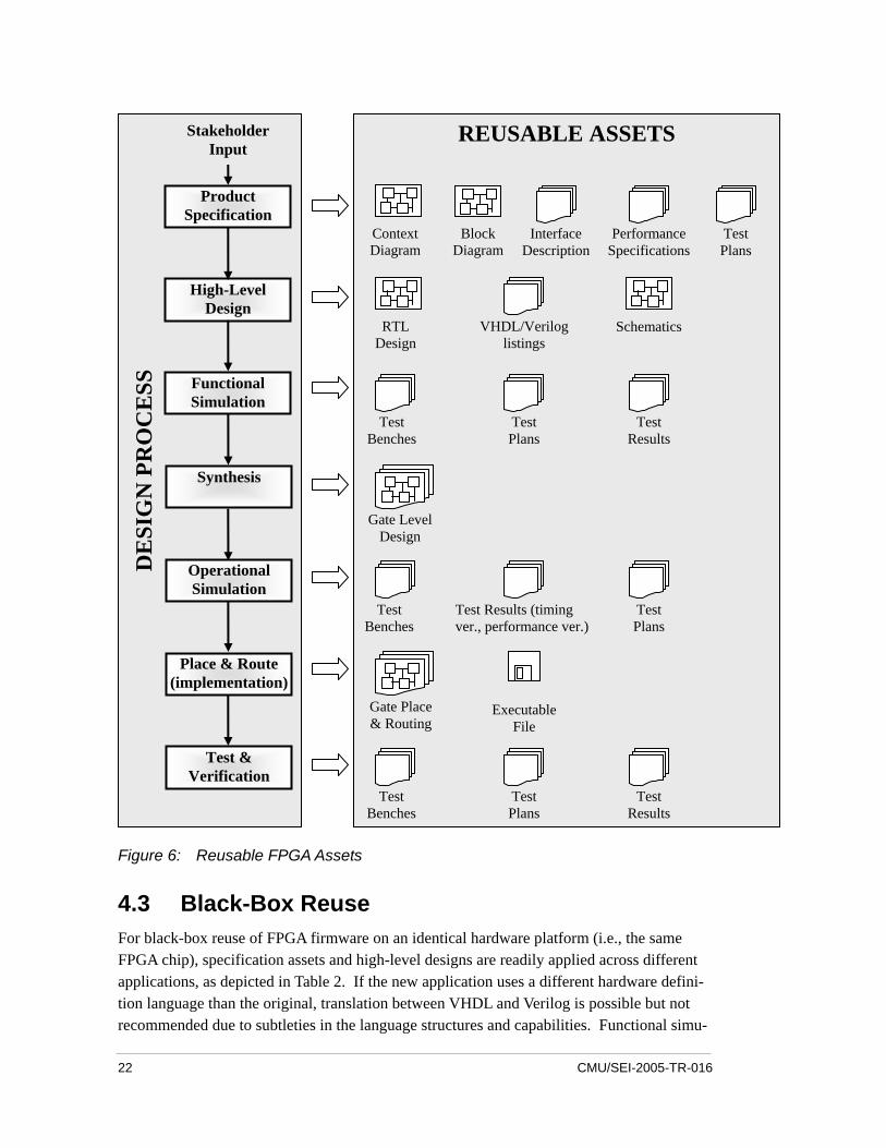
4.2 Reuse and FPGA Firmware In Section 3, we described a generic design process for FPGA firmware consisting of seven steps, each producing a collection of process outputs. Each of these process outputs is a po-tential reuse asset. The reusability of these assets depends highly upon the nature of the re-use, which may come in several forms. The most comprehensive form of reuse is reuse of the firmware on the same hardware platform for which it was developed; which enables the reuse of the broadest set of component assets. When reusing a component asset developed on a different hardware platform, fewer of the assets are reusable. Reusable component assets, as shown in Figure 6 consist of the following:
• specification assets
− context diagrams − block diagrams − performance specifications − interface specifications − test plans
• high-level design assets
− RTL designs − VHDL/Verilog listings − schematics
20 CMU/SEI-2005-TR-016
• functional simulation assets
− test benches − test plans − test results
• synthesis assets
− gate-level design • operational simulation assets
− test benches − test plans − test results
• implementation assets
− gate placement − routing
• test and verification assets
− test benches − test plans − test results
Depending on the nature of the reused component, the reuse may occur at various levels of abstraction. Components such as math libraries may be provided as VHDL or Verilog files, enabling their inclusion with the user’s source code. Embedded processors, with their more stringent timing requirements, may be provided fully implemented (e.g., synthesized, placed, and routed) for a specific FPGA. The availability of component assets is tied to this charac-teristic. Fully implemented components, such as those acquired from COTS software ven-dors, generally do not include documentation providing insight into the inner workings of the component−they are truly black-box components. Often, the only available documentation consists of the specification assets and perhaps some final test and verification assets.
CMU/SEI-2005-TR-016 21
Stakeholder Input
Product Specification
High-Level Design
Functional Simulation
Synthesis
Operational Simulation
Place & Route (implementation)
Test & Verification
DE
SIG
N P
RO
CE
SS
Test Plans
ContextDiagram
Block Diagram
Interface Description
Performance Specifications
RTL Design
VHDL/Verilog listings
Schematics
Test Benches
Test Plans
Gate Level Design
Test Benches
Test Results (timing ver., performance ver.)
Gate Place & Routing
Executable File
Test Benches
Test Plans
Test Results
Test Plans
Test Results
REUSABLE ASSETS
Figure 6: Reusable FPGA Assets
4.3 Black-Box Reuse For black-box reuse of FPGA firmware on an identical hardware platform (i.e., the same FPGA chip), specification assets and high-level designs are readily applied across different applications, as depicted in Table 2. If the new application uses a different hardware defini-tion language than the original, translation between VHDL and Verilog is possible but not recommended due to subtleties in the language structures and capabilities. Functional simu-
22 CMU/SEI-2005-TR-016
lation, synthesis, and operational simulation assets are also reusable. In general, implementa-tion and final test assets are less reusable due to the placement and routing process. Pre-determination of placement and routing for the reused elements can over-constrain the placement and routing of the remainder of the design and can lead to inefficient use of hard-ware resources.
Porting to different FPGAs is possible, but the number of assets that can be reused is reduced. Most specification assets are readily applied, with the exception of hardware-specific assets such as gate count estimates. Reuse of high-level design assets can be compromised by dif-ferent recommended coding styles for the different platforms. If the new application uses a different hardware definition language than the original, translation between VHDL and Ver-ilog is possible but not recommended due to subtleties in the language structures and capa-bilities. Functional simulation assets are reusable only to the extent that the high-level design assets are reusable. Synthesis assets are generally not reusable since the different target FPGA architecture forces a resynthesis and resimulation. Test results from operational simu-lation are not reusable since they no longer reflect testing of the current implementation. However operation simulation test assets such as test plans and test benches can be reusable. Implementation assets and final test results are not reusable. Test results from verification are not reusable; however, test assets such as test plans and test benches may be.
CMU/SEI-2005-TR-016 23
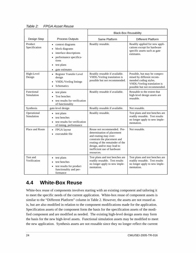
Table 2: FPGA Asset Reuse
Black-Box Reusability
Design Step Process Outputs Same Platform Different Platform Product Specification
• context diagrams • block diagrams • interface descriptions • performance specifica-
tions • test plans
• gate estimates
Readily reusable. Readily applied for new appli-cations except for hardware specific assets such as gate estimates.
High-Level Design
• Register Transfer Level design
• VHDL/Verilog listings • Schematics
Readily reusable if available. VHDL/Verilog translation is possible but not recommended.
Possible, but may be compro-mised by different recom-mended coding styles. VHDL/Verilog translation is possible but not recommended.
Functional Simulation
• test plans • Test benches • test results for verification
of functionality
Readily reusable if available. Reusable to the extent that high-level design assets are reusable.
Synthesis gate-level design Readily reusable if available. Not reusable.
Operational Simulation
• test plans • test benches • test results for verification
of timing, performance
Readily reusable. Test plans and test benches are readily reusable. Test results no longer apply to new imple-mentation.
Place and Route • FPGA layout • executable file
Reuse not recommended. Pre-determination of placement and routing may over-constrain the placement and routing of the remainder of the design, and/or may lead to inefficient use of hardware resources.
Not reusable.
Test and Verification
• test plans • test benches • test results for product
functionality and per-formance
Test plans and test benches are readily reusable. Test results no longer apply to new imple-mentation.
Test plans and test benches are readily reusable. Test results no longer apply to new imple-mentation.
4.4 White-Box Reuse White-box reuse of components involves starting with an existing component and tailoring it to meet the specific needs of the current application. White-box reuse of component assets is similar to the “Different Platform” column in Table 2. However, the assets are not reused as is, but are also modified in relation to the component modifications made for the application. Specification assets of the component form the basis for the specification assets of the modi-fied component and are modified as needed. The existing high-level design assets may form the basis for the new high-level assets. Functional simulation assets may be modified to meet the new application. Synthesis assets are not reusable since they no longer reflect the current
24 CMU/SEI-2005-TR-016
implementation. Test results from operational simulation are not reusable since they no longer reflect testing of the current implementation. However, operational simulation test assets such as test plans and test benches may be reusable with modification. Implementation assets and final test results are not reusable. Test results from verification are not reusable; however, test assets such as test plans and test benches may be reusable with modification.
CMU/SEI-2005-TR-016 25

26 CMU/SEI-2005-TR-016
5 Evaluating Reusability
A key question for both developers and acquirers is “How do I know whether or not a soft-ware component is reusable?” The answer to this question lies in the observable characteris-tics of the component. Both black-box and white-box components exhibit identifiable char-acteristics that impact their reusability.
5.1 Black-Box Reuse Two fundamental principles underlie the reusability of any black-box software asset. First, it must easily integrate into the overall design. Second, the component must be robust, with no internal verification needed. Software assets to be reused should exhibit certain characteris-tics. When discussing reuse of components in ASIC and System-on-Chip (SoC) design, the following characteristics have been identified [Keating 02]. The components must be
• designed to solve a general problem. Solutions to a specific, niche problem are unlikely to find applications for future reuse. On the other hand, only rarely is the problem to be solved today, exactly the same as the problem solved yesterday. Thus, the software asset must provide a generic solution to a general problem but must also incorporate flexibility to enable application to specific instantiations of the general problem.
• designed and built using good development practices. This includes the basics of com-plete, clear, structured documentation, clean code developed in accordance with coding standards, thorough source code comments, and well-designed, comprehensive verifica-tion support.
• compatible with a variety of verification environments and simulators. A software asset that can be verified by only one test bench or simulator creates a demand that the re-quired test asset be available for all uses of the asset. This severely limits the portability of the asset.
• designed in accordance with standard interfaces. Interfaces built to conform to published standards increase the portability of the software asset.
• comprehensively tested. Testing of the software asset must be thorough, exercising the asset in all modes with a wide range of inputs.
• completely documented. Documentation must include sufficient information to ensure understanding by the developers and the maintainers. It must address all capabilities, limitations, and constraints of the asset.
CMU/SEI-2005-TR-016 27
Many of these characteristics are equally applicable to FPGA reuse. Addressing a common problem ensures an adequate market to support the development of a robust component. Good development practices are essential to creating a reliable component. Verification sup-port is needed to ensure the operation and integration of the component into the target sys-tem. While comprehensive testing is essential to the development of a reusable component, it may not be observable by the user. For black-box reuse, complete and accurate documenta-tion is the most readily apparent characteristic of the component.
5.1.1 General Problem Solution The component must address a general problem; otherwise, there is no incentive to invest the time and resources needed to develop a reusable component. Common examples of black-box reusable components include
• embedded processors and DSPs
• function libraries (for example, math libraries)
• standard interfaces (for example, USB)
When considering reuse in your application, ask yourself if the problem you need to solve is a common problem. If so, a search for a black-box solution may be worthwhile. If not, it may be possible to partition your need into subcomponents, some unique to your application and some more generic, and then initiate a search for black-box solutions to the generic prob-lems.
5.1.2 Good Development Practices With black-box reuse, we may not have the luxury of detailed examination of the source code. An embedded processor is most likely provided in executable code for a specific FPGA. In such a case, we will have no insight into the code structure, code commenting, etc. However, we may have access to higher level documentation of the component. Using good development practices leaves “footprints” that we can see in this documentation. Among the characteristics we can search for are
• a well-documented architecture consisting of multiple views, descriptions of architecture elements, data flow descriptions
• detailed interface descriptions
• clear, consistent functional descriptions
• consistent, understandable variable naming
5.1.3 Verification Support Ultimately, the reused component is integrated with the remainder of the system, with verifi-cation performed at various stages. The lowest level of testing applied is at the level of the component. The reused component should include test assets (e.g. test plans and test
28 CMU/SEI-2005-TR-016
benches) to support this testing. Test assets should also be fully documented, including the purpose and methodology of the testing, acceptance and rejection criteria, and resources needed for execution.
5.1.4 Complete Documentation As stated previously, reuse involves more than just reusing code. Additional supporting documentation is needed to ensure sufficient understanding of the component and to facilitate application and integration of the code. For black-box reuse, typically we are concerned with a description of the component primarily from an external perspective. Assets supporting this perspective are the specification assets and a portion of the final test and verification assets, in particular, the test plans and test benches. Availability of these assets is crucial to the reuse of the component.
The specification assets should be clear, concise, and accurate. Context diagrams and block diagrams should be clear, with all elements and paths labeled and explained. Performance specifications should reflect the complete set of component functional and non-functional requirements. Interface specifications should be complete and accurate and should contain sufficient detail (signal characteristics, timing, etc.) to ensure proper interface with other components. Test plans should define the functions to be tested, the procedures used for test-ing, the resources needed for testing, and acceptance and rejection criteria. Test benches should be clearly linked to the test plans and should be fully documented and tested.
Additionally, IBM has developed a set of guidelines addressing what information is needed by developers to effectively reuse software components [Poulin 96]. While not directly ad-dressing FPGA firmware, these guidelines are relevant, and include the following elements:
• abstract to provide a concise and understandable description of the component
• change history to document the changes in the code, the reasons for the change, when they were made, and who made them
• description of dependencies that identifies other software assets needed for the use of this component
• design documents that describe the internal structure and function of the component, and include a rationale for major design decisions
• description of interfaces describing all component inputs and outputs
• legal summary defining legal information such as copyright and license restrictions
• performance specification defining timing, resource needs, and performance considera-tions of the component
• listing of restrictions defining limitations and special considerations regarding the use of the component
• application scenario illustrating the component’s application to a defined problem
• test documentation including test procedures, test cases, test history, and test results
CMU/SEI-2005-TR-016 29
5.2 White-Box Reuse When reusing a white-box component, we have more insight into the internal work-ings of the component. White-box components typically start as VHDL or Verilog code modules augmented by the component assets illustrated in
Figure 6: Reusable FPGA Assets
. These form the basis upon which we build the modifications needed to address the current application. Keys to successful reuse of white-box components are
• good development practices
• test support
• comprehensive testing
• complete documentation
5.2.1 Good Development Practices We start with the development footprints discussed for black-box reuse. The same character-istics should be observed for white-box components:
• a well-documented architecture consisting of multiple views, descriptions of architecture elements, data flow descriptions
• detailed interface descriptions
• clear, consistent functional descriptions
• consistent, understandable variable naming
• documented exception handling
Unlike with black-box reuse, we have the ability to view the internal workings of the compo-nent, enabling us to gain insight into the development practices employed to create the com-ponent. We can examine the design for evidence that good design practices were used at both a global and a local level.
At the global level, we want to verify that the design utilizes practices proven to be func-tional, reliable, and scalable. The design should also be as simple as possible. Design seg-mentation is critical to reusability. Partitioning the design into functional elements enhances understanding of the design and promotes fault isolation and testability by allowing anoma-lous operation to be localized for study and correction.
At the local level, more concrete characteristics can be observed:
• Designs should be synchronous in nature. Latches should be avoided in favor of clocked flip-flops and registers. Delays should be instantiated through dedicated delay elements, not via gate delays. Race conditions should be avoided by elimination of feed-back in combinatorial logic. Logic feedback should first be synchronized with a clocked element prior to feedback. Finally, clocks should not be gated. The exception to this is if
30 CMU/SEI-2005-TR-016
clock gating is used to disable an entire block of inactive circuitry for reasons of power conservation.
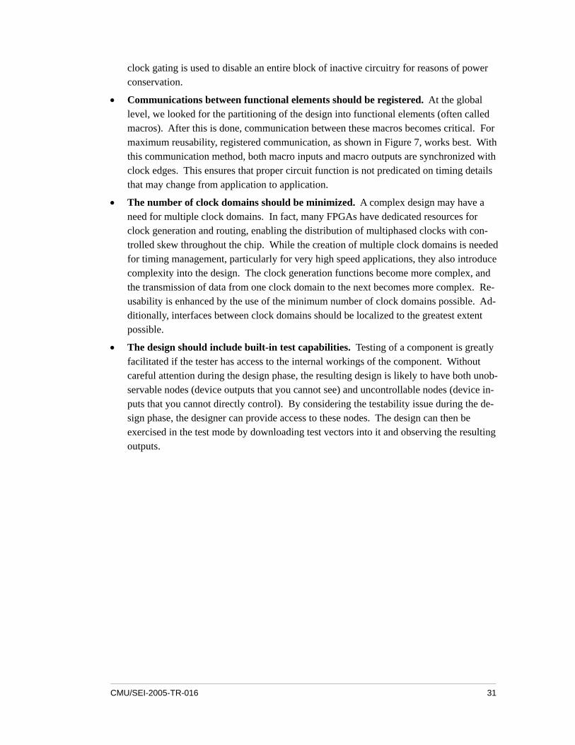
• Communications between functional elements should be registered. At the global level, we looked for the partitioning of the design into functional elements (often called macros). After this is done, communication between these macros becomes critical. For maximum reusability, registered communication, as shown in Figure 7, works best. With this communication method, both macro inputs and macro outputs are synchronized with clock edges. This ensures that proper circuit function is not predicated on timing details that may change from application to application.
• The number of clock domains should be minimized. A complex design may have a need for multiple clock domains. In fact, many FPGAs have dedicated resources for clock generation and routing, enabling the distribution of multiphased clocks with con-trolled skew throughout the chip. While the creation of multiple clock domains is needed for timing management, particularly for very high speed applications, they also introduce complexity into the design. The clock generation functions become more complex, and the transmission of data from one clock domain to the next becomes more complex. Re-usability is enhanced by the use of the minimum number of clock domains possible. Ad-ditionally, interfaces between clock domains should be localized to the greatest extent possible.
• The design should include built-in test capabilities. Testing of a component is greatly facilitated if the tester has access to the internal workings of the component. Without careful attention during the design phase, the resulting design is likely to have both unob-servable nodes (device outputs that you cannot see) and uncontrollable nodes (device in-puts that you cannot directly control). By considering the testability issue during the de-sign phase, the designer can provide access to these nodes. The design can then be exercised in the test mode by downloading test vectors into it and observing the resulting outputs.
CMU/SEI-2005-TR-016 31
MACRO 1
regi
ster
Macro logic re
gist
er MACRO 2
regi
ster
Macro logic re
gist
er
MACRO 1
regi
ster
Macro logic
MACRO 2
regi
ster
Macro logic re
gist
er
MACRO 1
regi
ster
Macro logic re
gist
er MACRO 2
Macro logic re
gist
er
BAD
BAD
GOOD
Figure 7: Macro I/O Registration
5.2.2 Test Support Test plans, test benches, and test results from functional, operational, and final testing for the original design are all helpful in developing their counterparts for the modified design. Each of these component assets will form the basis of the associated modified asset; as such, the quality of the original asset is important.
Test plans should define the functions to be tested, the procedures used for testing, the re-sources needed for testing, and accept/reject criteria. Test benches should be clearly linked to the test plans and should be fully documented and tested. Test results cannot be reused; how-ever, they can be helpful in understanding the execution of the test plans and may even pro-mote understanding of the component functionality.
5.2.3 Comprehensive Testing The component must be tested comprehensively. Test plans, test benches, and test results should be available from functional simulation, operational simulation, and final test and verification. These test plans and test benches form the basis for the test plans and test benches for the modified component. They should be understandable and well documented.
In addition to verifying the intended functionality of the component, testing should also ad-dress robustness issues such as
• performance under peak load or stress
32 CMU/SEI-2005-TR-016
• error detection and correction
• input boundaries and validity
• interfaces to other components
• conversions/limits/corner conditions
• timing/synchronization
5.2.4 Complete Documentation For black-box reuse, as discussed in Section 5.1.4, the desired documentation should focus on a description of the component from an external perspective. The same documentation mentioned for black-box reuse should also be available for white-box reuse. With greater insight into the internal workings of the component afforded by white-box reuse, we have access to a wider range of documentation. In addition to the specification assets and some of the verification assets, we should also have access to high-level design assets and perhaps functional simulation and synthesis assets.
The specification assets should be clear, concise, and accurate. Context diagrams and block diagrams should be clear, with all elements and paths labeled and explained. Performance specifications should reflect the complete set of component functional and non-functional requirements. Interface specifications should be complete and accurate and should contain sufficient detail (signal characteristics, timing, etc.) to ensure proper interface with other components.
The high-level design assets should include VHDL/Verilog listings representing the design at the RTL level. This source code should be fully commented. Comments should include headers for each functional element describing the operation of that element. Consistent and understandable naming conventions should be used throughout the component.
Test plans at all levels (i.e., functional, operational, and final) should define the functions to be tested, the procedures used for testing, the resources needed for testing, and acceptance and rejection criteria.
Test benches at all levels should be linked to test plans, and should be fully documented and tested.
CMU/SEI-2005-TR-016 33

34 CMU/SEI-2005-TR-016
6 Encouraging Reuse and Reusability
Encouraging reuse and encouraging reusability are two independent but related activities. By encouraging reuse, you are promoting the use of existing components in your current design. By encouraging reusability, you are promoting the development of current designs that have the potential for future reuse.
Development organizations often have a stake in firmware reuse. Reuse has the potential to reduce development time, reduce development cost, and improve product quality. Thus, managers of development organizations often play a role in encouraging both reuse and reus-ability. This encouragement within development organizations typically takes the form of company policy or technical direction.
Acquiring organizations also have a stake in firmware reuse for the same reasons—reduced time and cost and increased product quality. Furthermore, reusing components from other systems can have a favorable impact on interoperability among those systems. Thus, acquir-ers often play a role in encouraging reuse and reusability. This encouragement within acquir-ing organizations is typically expressed in the form of requirements or contracts.
6.1 Barriers to Reuse With all of the benefits attainable from reuse, why is it not universally practiced? A number of barriers, both technical and non-technical, must first be overcome [Reifer 97].
Reuse is most effective when pursued as part of a software product line. Product line devel-opment begins with a domain analysis to understand the needs of the market to be served be-yond the current project. Based upon the results of this analysis, a product line architecture may be developed. The architecture can then be populated with different sets of reusable components to satisfy the diverse needs of the broader market. The development of a product line architecture and the components to populate it is a technically challenging activity. In many cases, the program staff lacks the expertise and the experience to perform a domain analysis, and many are unfamiliar with open systems architectures and standards-based inter-faces.
Organizational issues can also impede reuse. Management often exhibits a project-by-project mentality, focusing program staff on the success of the current project, not the longer-term goal of product line development. Time and resources commensurate with solving the im-mediate problem are allocated but are insufficient to address the longer-term problem. Addi-tionally, many organizations lack the infrastructure to support product line development and
CMU/SEI-2005-TR-016 35
reuse. Many software engineering environments lack robust tools (library support, analyzers, etc.) to support reuse.
Psycho-social factors may also play a role. Developers often enjoy the creative aspects of their work. Although more efficient, modifying existing components is often viewed as being less satisfying work than creating new ones. Reuse also demands trust. The developer’s competence and performance will be measured based upon the performance of the new de-sign. With reuse, the developer is incorporating work that others have performed into the new design. As such, the developer is placing trust in the work of others—a choice that is not without risk and some discomfort from their perspective.
6.2 Promoting Reuse
6.2.1 In a Development Organization Promoting reuse in a development organization is not very difficult. In fact, most competent developers do not need to be encouraged to reuse components; they will do so naturally, driven by the desire for shorter development times, reduced development costs, and improved product quality.
In a development organization, financial incentives for reuse are often inherent in the opera-tion, if not always apparent. If reuse enables developers to provide products faster, better, and cheaper, developers who employ effective reuse strategies consistently exhibit better per-formance by being under budget and on time for their projects. In most development organi-zations, superior performance is recognized and rewarded.
6.2.2 In an Acquisition Organization From the perspective of an acquisition organization, incentives for developers to employ re-use strategies are not inherent, but must be explicitly addressed by using vehicles such as contract type, award fees, incentive fees, etc.
In some sense, the role of the acquirer is to
• ensure the presence of financial incentives (and the absence of financial disincentives) for the developer to take advantage of reuse opportunities
• ensure the presence of technical incentives (and the absence of technical disincentives) for the developer to reuse components
The acquirer must maintain a clear focus on the real goal, which is not to encourage reuse but to encourage appropriate reuse. Without this distinction, it is possible that contractual incen-tives for reuse results in the supplier reusing inappropriate components solely to meet the cri-teria of the reuse incentives. Such reuse may not achieve the desired benefits of shorter de-velopment times, reduced development costs, and improved product quality, and can actually
36 CMU/SEI-2005-TR-016
be detrimental. In reality, the acquirer must incentivize the performance of trade studies to identify and evaluate reuse opportunities.
Inadvertently, acquirers may provide financial disincentives for the reuse of existing compo-nents. Simply by using a cost-reimbursable contract (cost plus fixed fee (CPFF) or cost plus incentive fee (CPIF)), the acquirer may be discouraging reuse. If the supplier’s compensation depends on the amount of work done, there is no incentive to reduce development effort through reuse. This is not to imply that these types of contract are inappropriate for many firmware development efforts. The desire to encourage reuse is only one of the factors driv-ing the acquirer’s selection of contract type. Other factors such as overall complexity and stability of requirements, which also drive the selection of contract type, may have an over-riding influence on the selection of a contract type. In this event, if a cost-reimbursable con-tract is implemented the acquirer must be aware that it may not provide the desired encour-agement of reuse. The acquirer must then address the reuse issue directly through other language within the contract. In a competitive bid, this is sometimes accomplished by requir-ing the potential suppliers to define in their proposals the expected magnitude of reuse and the cost savings associated with the reuse. Award fees and incentive fees are then tied to meeting these objectives. The deficiency in this strategy, as noted in the previous paragraph, is that it may result in the contractor reusing inappropriate components solely to meet the in-centivized reuse criteria. A better strategy is to use award fees and incentive fees to encour-age trade studies of reuse opportunities, and negotiate cost sharing agreements for savings resulting from reuse.
Similarly, the acquirer may provide technical disincentives for reuse through overly prescrip-tive requirements. In the case where requirements promote a specific solution (or worse, ex-plicitly require a specific solution), an alternative solution more supportive of reuse of exist-ing components is eliminated. The supplier is pushed into a non-reuse strategy. This underscores the importance of proper requirements engineering: development of require-ments that define what is to be done, rather than how to do it.
Issues such as licensing and data rights can also affect reuse strategies. Consider the case where the acquirer requires full data rights to all delivered items. Perhaps existing compo-nents are available and appropriate for reuse, but they are only available with limited data rights. In this case, the result again is that the supplier is pushed into a non-reuse strategy. Make sure that the licensing and data rights clauses of your contract are sufficiently flexible to address these reuse issues.
6.3 Promoting Reusability Promoting reusability is a bit more difficult, in that the acquirer must play a more active role to incentivize the supplier to create reusable products. This incentivization is done through both contracting actions and technical requirements.
CMU/SEI-2005-TR-016 37
Achieving reusability in a product begins at the earliest stages of project initiation. As noted in Section 1.1, production of a fully reusable product may require as much as ten times the effort to produce a single-use product. Clearly this must be comprehended during the initial project planning and budgeting.
Identification of reusability needs is a key factor in successful reuse. The acquirer must de-fine the components for which reusability is desired, taking care not to be too extravagant, since development of reusable components requires additional time and resources.
Defining reuse parameters is also necessary. Is the component intended to be reused on an equivalent hardware platform or a different platform? Is the goal black-box reuse or white-box reuse? How much modification is anticipated or allowed for white-box reuse? Will the component be reused in the same domain for which it was developed, or will it be used in a new domain?
The acquirer should provide guidance for the documentation of reusable components. For black-box reuse, specification assets such as context diagrams, block diagrams, performance specifications, interface specifications, and test plans should be required and their contents should be mandated. Final test and verification assets such as test plans and test benches should also be required and their contents mandated. For white-box reuse, in addition to the previous assets, the acquirer should also require
• high-level design assets (RTL designs, VHDL/Verilog listings, schematics)
• functional simulation assets (test benches, test plans, test results)
• synthesis assets1 (gate-level designs)
• operational simulation assets (test benches, test plans, test results1)
• test and verification assets (test benches, test plans, test results1)
At design reviews, the acquirer should examine component designs for the characteristics cited in Section 5.2.1 (synchronous design, registered inter-block communication, minimal clock domains, built-in test) to verify good design practices. Coding standards and styles should also be defined and enforced.
1 These assets are required when the reusable component is used on the same hardware platform.
38 CMU/SEI-2005-TR-016
7 Summary
Reuse of FPGA firmware, like other forms of software reuse, can provide benefits such as reduced cost, shortened delivery time, and improved product quality. Like reuse of other software components, firmware reuse requires a detailed understanding of the functionality and the interfaces of the component to be reused and involves the reuse of not only the result-ing code, but also the supporting documentation.
Good development practices are the hallmark of reuse. Firmware reuse is most effective when planned for during component development. Specific practices such as synchronous design, registered communications between functional elements, minimization of the number of clock domains, and the inclusion of built-in test capabilities greatly enhance reusability.
Test support, comprehensive component testing, and complete documentation are the other key factors enabling reuse.
An acquirer can promote reuse through the use of financial and technical incentives that en-courage developers to take advantage of reuse opportunities. However, the acquirer must maintain a clear focus on the real goal, which is not to encourage reuse, but to encourage ap-propriate reuse. As such, it is seldom appropriate to establish a goal for a specified level of reuse. Rather, the acquirer should use contract incentives (e.g., award fees, incentive fees) to encourage the performance of trade studies of reuse opportunities. It is also necessary to en-sure appropriate data rights and the delivery of the complete documentation needed to sup-port future reuse.
CMU/SEI-2005-TR-016 39

40 CMU/SEI-2005-TR-016
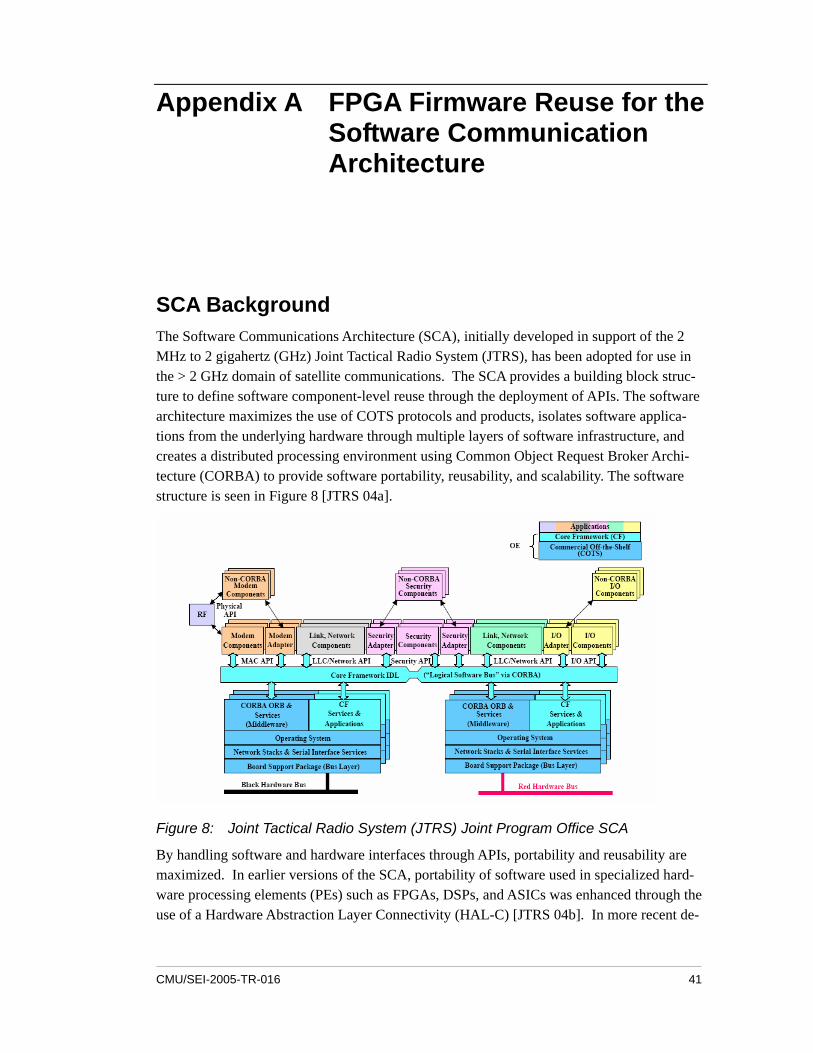
Appendix A FPGA Firmware Reuse for the Software Communication Architecture
SCA Background The Software Communications Architecture (SCA), initially developed in support of the 2 MHz to 2 gigahertz (GHz) Joint Tactical Radio System (JTRS), has been adopted for use in the > 2 GHz domain of satellite communications. The SCA provides a building block struc-ture to define software component-level reuse through the deployment of APIs. The software architecture maximizes the use of COTS protocols and products, isolates software applica-tions from the underlying hardware through multiple layers of software infrastructure, and creates a distributed processing environment using Common Object Request Broker Archi-tecture (CORBA) to provide software portability, reusability, and scalability. The software structure is seen in Figure 8 [JTRS 04a].
Figure 8: Joint Tactical Radio System (JTRS) Joint Program Office SCA
By handling software and hardware interfaces through APIs, portability and reusability are maximized. In earlier versions of the SCA, portability of software used in specialized hard-ware processing elements (PEs) such as FPGAs, DSPs, and ASICs was enhanced through the use of a Hardware Abstraction Layer Connectivity (HAL-C) [JTRS 04b]. In more recent de-
CMU/SEI-2005-TR-016 41
velopments, the tendency is to replace the proprietary HAL-C interfaces with interfaces de-veloped in compliance with the Open Core Protocol (OCP) standard.
Open Core Protocol The OCP was designed to facilitate communications between functional elements, often called intellectual property (IP) cores, which comprise a system on a chip. A major benefit of OCP is that it provides independence from bus protocols, while maintaining high-performance access to on-chip interconnects between IP cores. The ability to design IP cores independent of their interfaces to the target system greatly increases the reusability of these cores. To maintain sufficient flexibility to address the wide range of IP cores, the OCP inter-faces are highly configurable.
Fundamental concepts of the OCP include the following:
• point-to-point synchronous interface – all signals are unidirectional and sampled at the rising edge of the OCP clock
• bus independence – an OCP compliant core can be interfaced to any on-chip bus
• commands – the OCP implements a limited series of commands, consisting of basic commands of Read and Write and command extensions WriteNonPost, Broadcast, ReadExclusive, ReadLinked, and WriteConditional
• address/data – data and address bus widths are configurable
• pipelining – pipelining of transfers is supported
• response – requests and responses are separated in OCP. Responses can be immediate, delayed, or eliminated (e.g., for pipelining).
• burst – burst transfers are supported. Bursts can include addressing information for each successive command or can include addressing information only at burst initiation.
• tags – data transfers can be “tagged” (i.e., labeled with a unique identifier), enabling re-quests and responses to be transferred out of order, without loss of meaning
• threads and connection – the OCP supports multiple threads to support concurrency and out-of-order processing of transfers. Transactions within different threads are independ-ent, with no cross-thread ordering requirements; however, transfers within a single thread remain ordered unless tags are in use.
• interrupts, errors, and other sideband signaling – the OCP supports control signaling independent of address/data transfers
The OCP interface signals are classified as dataflow, sideband, or test signals. Dataflow sig-nals are further subdivided into basic, simple extensions, burst extensions, tag extensions, and thread extensions. All OCP signals are point to point, unidirectional, and synchronous with the rising edge of the OCP clock. As an example, the dataflow basic signals are shown in Table 3.
42 CMU/SEI-2005-TR-016
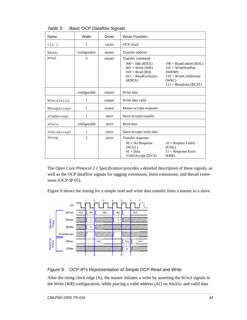
Table 3: Basic OCP Dataflow Signals
Name Width Driver Driver Function
Clk 1 1 varies OCP clock
MAddr configurable master Transfer address
Transfer command MCmd 3 master 000 = Idle (IDLE) 001 = Write (WR) 010 = Read (RD) 011 = ReadExclusive (RDEX)
100 = ReadLinked (RDL) 101 = WriteNonPost (WRNP) 110 = WriteConditional (WRC) 111 = Broadcast (BCST)
configurable master Write data
MDataValid 1 master Write data valid
MRespAccept 1 master Master accepts response
SCmdAccept 1 slave Slave accepts transfer
SData configurable slave Read data
SDataAccept 1 slave Slave accepts write data
Transfer response SResp 2 slave 00 = No Response (NULL) 01 = Data Valid/Accept (DVA)
10 = Request Failed (FAIL) 11 = Response Error (ERR)
The Open Core Protocol 2.1 Specification provides a detailed description of these signals, as well as the OCP dataflow signals for tagging extensions, burst extensions, and thread exten-sions [OCP-IP 05].
Figure 9 shows the timing for a simple read and write data transfer from a master to a slave.
Figure 9: OCP-IP’s Representation of Simple OCP Read and Write
After the rising clock edge (A), the master initiates a write by asserting the MCmd signals in the Write (WR) configuration, while placing a valid address (A1) on MAddr and valid data
CMU/SEI-2005-TR-016 43
(D1) on MData. In response, the slave immediately asserts the SCmdAccept signal, indi-cating that it is prepared to capture the address and data on the next rising clock edge. At the rising clock (B) the slave captures the address and data, while the master responds to the SCmdAccept signal and releases both the MAddr and MData signals.
The master initiates a read operation at clock edge (C) by asserting the MCmd signals in the Read (RD) configuration while placing a valid address (A2) on MAddr. In response, the slave immediately asserts the SCmdAccept signal, indicating that it is prepared to capture the address on the next rising clock edge. At the rising clock (D), the slave captures the ad-dress and decodes it to determine the data source to be read. When the data is ready for transmit, the slave asserts the DataValid/Accept (DVA) code on the SResp signal lines and places the data (D2) on the SData lines. The master captures the data (D2) at the rising clock (E) and de-asserts the SCmdAccept signal. At rising clock (E), the slave releases the SData and SResp lines.
The Open Core Protocol 2.1 Specification provides a detailed description of this transfer tim-ing, as well as the timing for other transfer types (e.g., handshake, burst, pipeline) [OCP-IP 05].
The operation of an OCP interface may also be viewed as a state machine. Figure 10 illus-trates a medium-throughput, high-frequency master-slave interface that uses a completely sequential design.
44 CMU/SEI-2005-TR-016
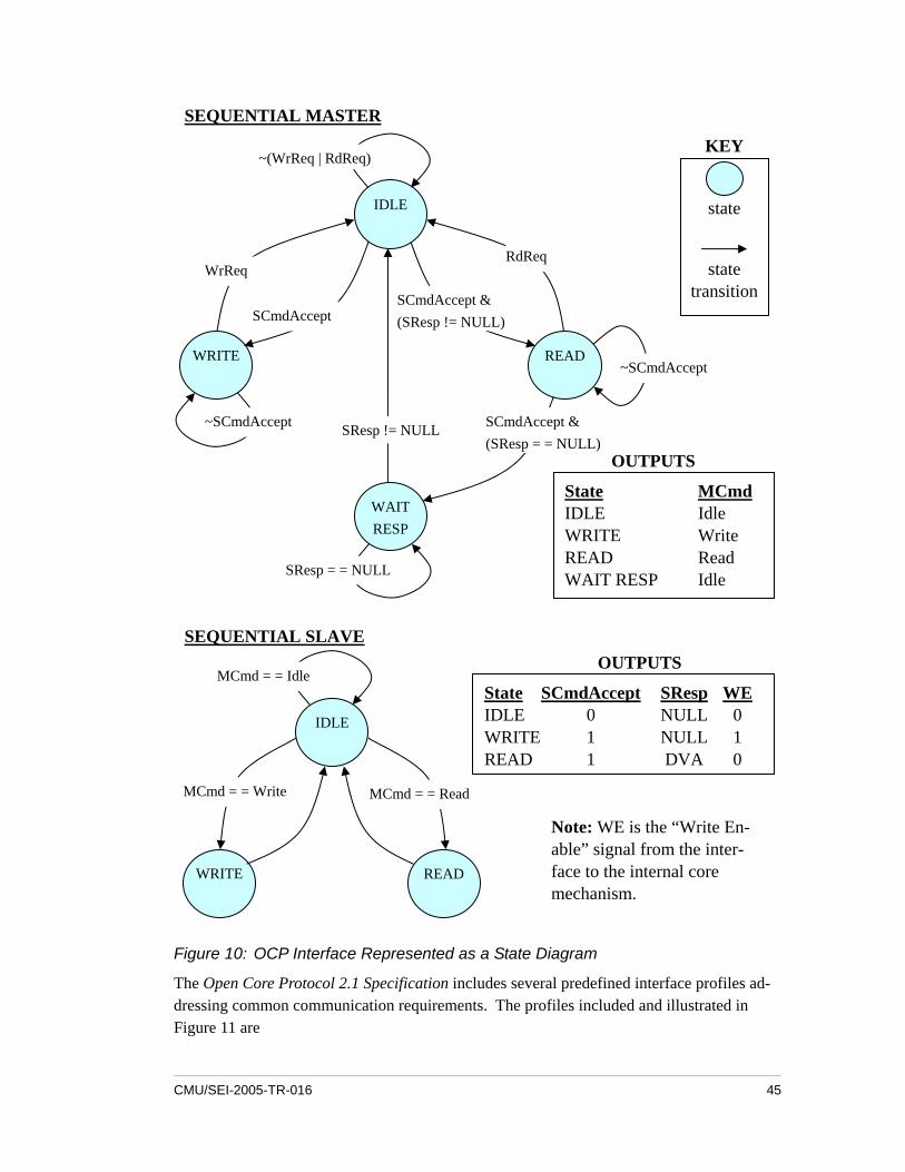
SEQUENTIAL MASTER
IDLE
WAIT RESP
READWRITE
WrReq
SCmdAccept
SCmdAccept & (SResp = = NULL)
SResp != NULL
SResp = = NULL
state
state transition
KEY
~SCmdAccept
OUTPUTS
State MCmd IDLE Idle WRITE Write READ Read WAIT RESP Idle
SCmdAccept & (SResp != NULL)
RdReq
~SCmdAccept
~(WrReq | RdReq)
SEQUENTIAL SLAVE
IDLE
READWRITE
OUTPUTS
State SCmdAccept SResp WE IDLE 0 NULL 0 WRITE 1 NULL 1 READ 1 DVA 0
MCmd = = Idle
MCmd = = Write MCmd = = Read
Note: WE is the “Write En-able” signal from the inter-face to the internal core mechanism.
Figure 10: OCP Interface Represented as a State Diagram
The Open Core Protocol 2.1 Specification includes several predefined interface profiles ad-dressing common communication requirements. The profiles included and illustrated in Figure 11 are
CMU/SEI-2005-TR-016 45
• block data flow − a master type interface for the exchange of data blocks with memory. It is suitable for pipelining defined-length traffic (e.g., MPEG macro blocks) to and from memory.
• sequential undefined length data flow − a master type interface for data streams com-munication with memory
• register access − an interface providing a control processor with the ability to program the operation of an attached core, such as a DMA engine
• simple H-bus − a bridge to other interface profiles; for example, to a central processing unit (CPU) using an Advanced Microcontroller Bus Architecture (AMBA™) Advanced High-performance Bus (AHB) protocol. The H-bus profile creates an OCP master wrap-per for native CPU interfaces performing multiple-request/multiple-data read and write transactions.
• X-bus packet write − supports instruction and data traffic (cacheable and non-cacheable) between a CPU and the memories and register interfaces of other targets. The “write” profile creates an OCP master wrapper for native CPU interfaces performing single-request/multiple-data write-only transactions.
• X-bus packet read − supports instruction and data traffic (cacheable and non-cacheable) between a CPU and the memories and register interfaces of other targets. The “read” profile creates an OCP master wrapper for native CPU interfaces performing single-request multiple-data read-only transactions.
The Open Core Protocol 2.1 Specification contains detailed information about the implemen-tation of each of these interface profiles [OCP-IP 05].
46 CMU/SEI-2005-TR-016
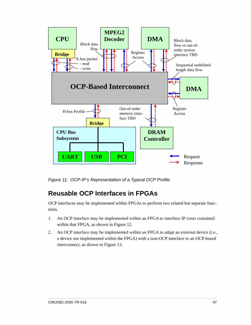
Request Response
CPU Bus Subsystem
OCP-Based Interconnect
CPU
MPEG2 Decoder
DMA
DRAM Controller
UART USB PCI
Bridge
Bridge
Out-of-order memory inter-face TBD
H-bus Profile
X-bus packet - read - write
Block data flow
Register Access
DMA
Register Access
Block data flow or out-of-order system interface TBD
Sequential undefilength data flow
ned
Figure 11: OCP-IP’s Representation of a Typical OCP Profile
Reusable OCP Interfaces in FPGAs OCP interfaces may be implemented within FPGAs to perform two related but separate func-tions.
1. An OCP interface may be implemented within an FPGA to interface IP cores contained within that FPGA, as shown in Figure 12.
2. An OCP interface may be implemented within an FPGA to adapt an external device (i.e., a device not implemented within the FPGA) with a non-OCP interface to an OCP-based interconnect, as shown in Figure 13.
CMU/SEI-2005-TR-016 47
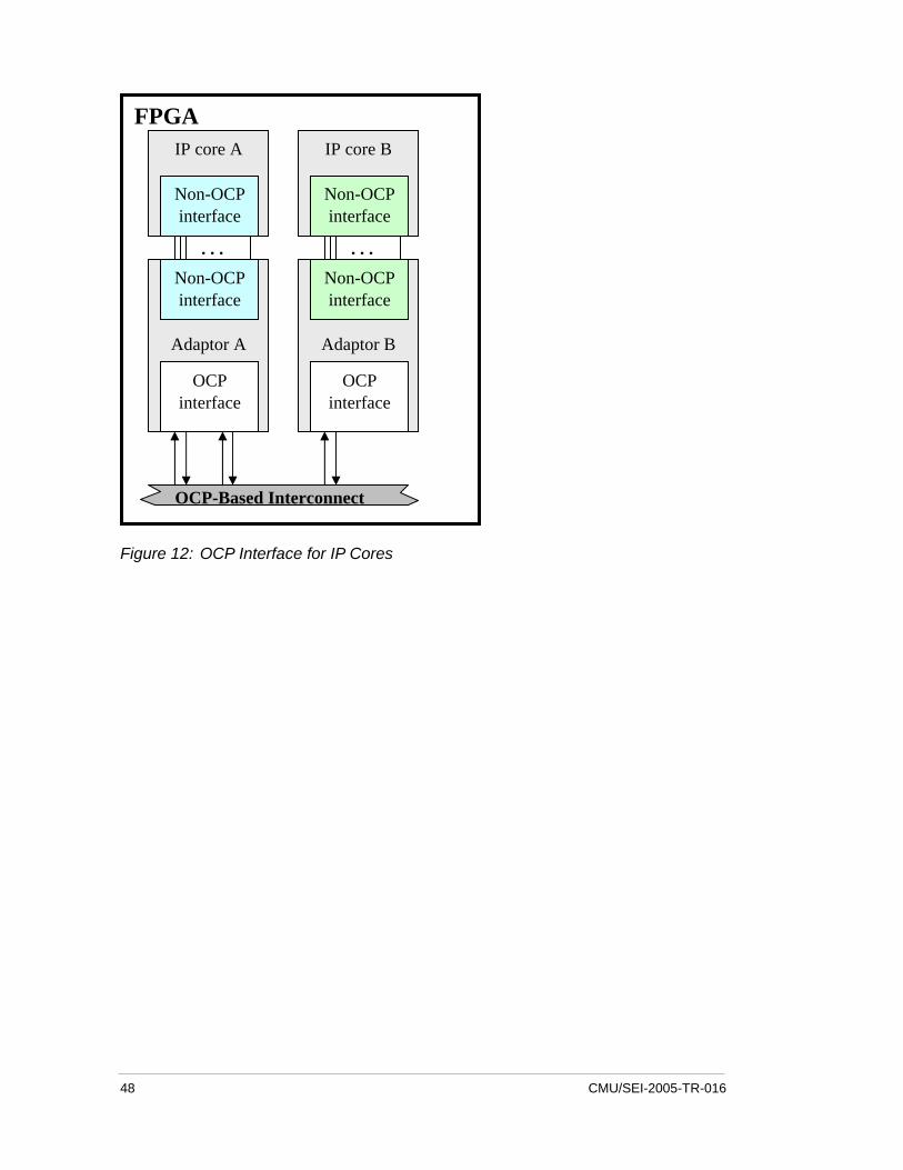
FPGA IP core A
Non-OCP interface
Adaptor A
OCP interface
. . .
Adaptor B
OCP interface
. . .
OCP-Based Interconnect
Non-OCP interface
Non-OCP interface
Non-OCP interface
IP core B
Figure 12: OCP Interface for IP Cores
48 CMU/SEI-2005-TR-016
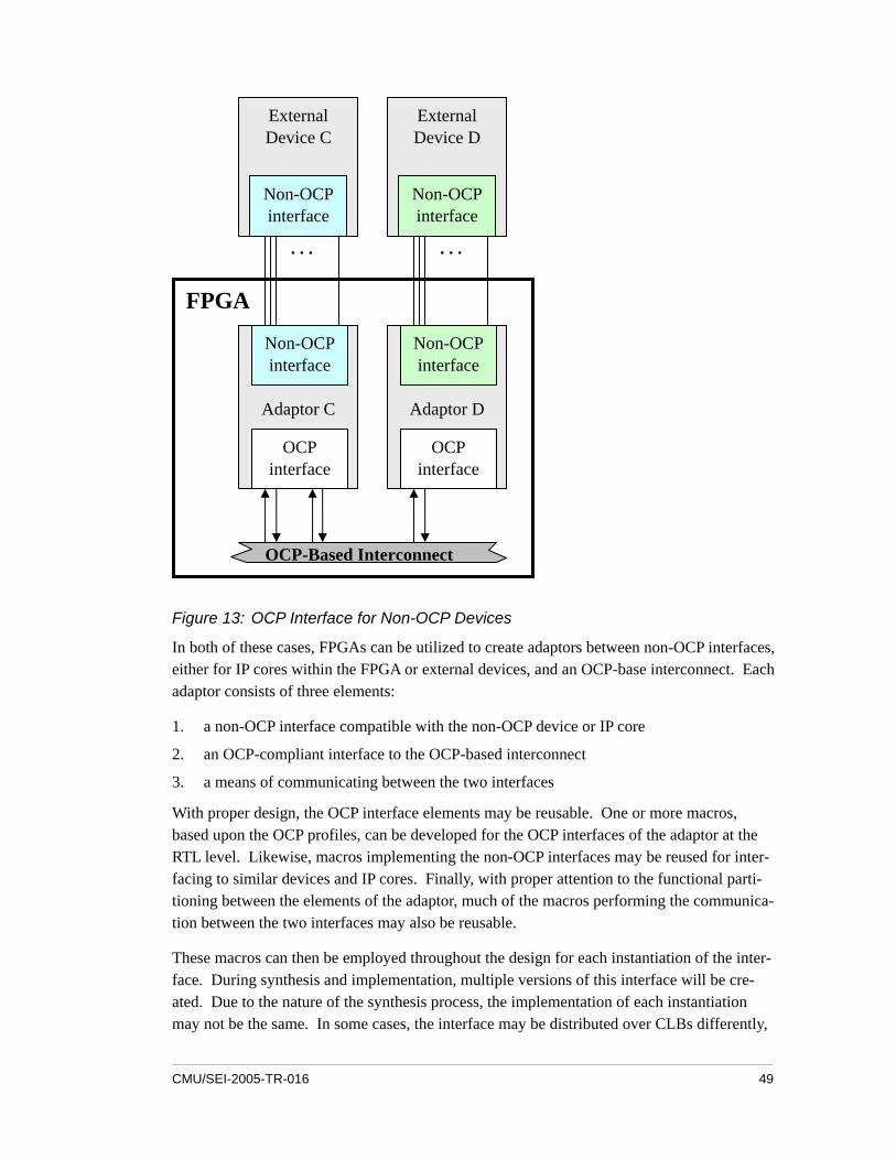
FPGA
External Device D
Adaptor D
Non-OCP interface
Adaptor C
OCP interface
OCP interface
OCP-Based Interconnect
. . . . . .
Non-OCP interface
Non-OCP interface
Non-OCP interface
External Device C
Figure 13: OCP Interface for Non-OCP Devices
In both of these cases, FPGAs can be utilized to create adaptors between non-OCP interfaces, either for IP cores within the FPGA or external devices, and an OCP-base interconnect. Each adaptor consists of three elements:
1. a non-OCP interface compatible with the non-OCP device or IP core
2. an OCP-compliant interface to the OCP-based interconnect
3. a means of communicating between the two interfaces
With proper design, the OCP interface elements may be reusable. One or more macros, based upon the OCP profiles, can be developed for the OCP interfaces of the adaptor at the RTL level. Likewise, macros implementing the non-OCP interfaces may be reused for inter-facing to similar devices and IP cores. Finally, with proper attention to the functional parti-tioning between the elements of the adaptor, much of the macros performing the communica-tion between the two interfaces may also be reusable.
These macros can then be employed throughout the design for each instantiation of the inter-face. During synthesis and implementation, multiple versions of this interface will be cre-ated. Due to the nature of the synthesis process, the implementation of each instantiation may not be the same. In some cases, the interface may be distributed over CLBs differently,
CMU/SEI-2005-TR-016 49
and CLBs may contain both elements of the interface and surrounding component functions. This method offers the most efficient utilization of the FPGA CLBs and routing resources.
Alternatively, the macro designs may be captured after synthesis. Each macro can be de-signed at the RTL level, functionally simulated, and synthesized. During synthesis of the en-tire design, these gate-level macro designs may be instantiated multiple times as needed and linked with the remainder of the design. When done in this manner, all instantiations of the macros will be distributed among CLBs in the same way; however, the instantiations of the macros may still exhibit minor performance variations due to the realization in CLBs distrib-uted throughout the FPGA by the place and route process. While this method provides more consistent performance among the macros, it provides for less efficient utilization of CLBs, and may overly constrain the place and route process.
To gain yet more control over the multiple macro instantiations, we can capture the macro design at the implementation level, after placement and routing. Each macro can be designed at the RTL level, functionally simulated, synthesized, operationally simulated, placed, and routed. During synthesis, placement, and routing of the entire design, these detailed imple-mentations of the interface designs may be instantiated multiple times as needed and linked with the remainder of the design. In this case, each interface would be implemented by a contiguous set of CLBs with defined signal routes. While this method provides the most consistent performance among the interfaces, it provides for less efficient utilization of CLBs, and may result in significant placement and routing challenges caused by local con-gestion.
Beyond OCP While OCP is a powerful method of encouraging software reuse, it is a necessary but not suf-ficient method. In addition to the interface constraints inherent in OCP, system designers must coordinate and constrain the interface options available within OCP, as well as the inter-face attributes not addressed by OCP.
Configurations and Options Within OCP Numerous options and configuration choices are found within the OCP specification. Inter-face designers can configure the width of the address data, the width of the transmit data, the width of the receive data, etc. They may choose to support different transfer types such as Write, Read, ReadEx, WriteNonPost, etc. The OCP specification contains numerous options for extensions to the basic signal set to provide support for burst data transfers, tagged data transfers, thread transfers, and so on. In addition to the preceding options of the basic OCP signals, the OCP specification also identifies a number of options for sideband signals and test signals. Furthermore, timing and speed of response must also be considered.
For each individual interface, these configurations and options within the OCP specification must be clearly defined. A data source with a 7-bit-wide address transmitting 32-bit-wide
50 CMU/SEI-2005-TR-016
data is not likely to communicate effectively with a data receiver expecting a 12-bit-wide ad-dress and 16-bit-wide data. A data source producing outputs at a 1 MHz rate will not com-municate effectively with a data receiver capable of processing data at a 1 kilohertz (KHz) rate.
The interface specification for each interface must fully define the OCP configurations and options. These attributes must be analyzed for consistency and sufficiency by the system de-velopers and communicated clearly to the component and interface developers.
Non-OCP Interface Attributes Always bear in mind that the OCP specification governs the interface details pertaining to the exchange of data. The specification does not address issues of data format or data interpreta-tion. Data format between IP cores must be consistent and managed. Numeric (e.g., fixed-point or floating-point) and text (e.g., ASCII) formats must be compatibly defined on all sides of the interface. Data interpretation must also be defined (e.g., does the numeric value trans-mitted across an interface represent the radio frequency (RF) carrier frequency in Hz or in MHz?).
The interface specification for each interface must fully define the data formats and the data meaning for all transmitted and received data. These attributes must be analyzed for consis-tency and accuracy by the system developers and communicated clearly to the component and interface developers.
CMU/SEI-2005-TR-016 51

52 CMU/SEI-2005-TR-016
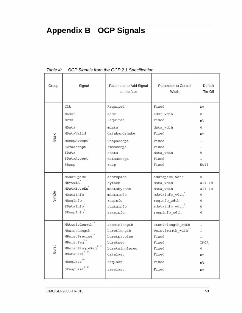
Appendix B OCP Signals
Table 4: OCP Signals from the OCP 2.1 Specification
Group
Signal
Parameter to Add Signal
to Interface
Parameter to Control
Width
Default
Tie-Off
Clk Required Fixed n/a
MAddr addr addr_wdth 0
MCmd Required Fixed n/a
MData mdata data_wdth 0
MDataValid datahandshake Fixed n/a
MRespAccept1
respaccept Fixed 1
SCmdAccept cmdaccept Fixed 1
SData1
sdata data_wdth 0
SDataAccept2
dataaccept Fixed 1
SResp resp Fixed Null
Bas
ic
MAddrSpace addrspace addrspace_wdth 0
MByteEn3
byteen data_wdth all 1s
MDataByteEn4
mdatabyteen data_wdth all 1s
MDataInfo mdatainfo mdatainfo_wdth5
0
MReqInfo reqinfo reqinfo_wdth 0
SDataInfo1
sdatainfo sdatainfo_wdth6
0
SRespInfo1
respinfo respinfo_wdth 0
Sim
ple
MAtomicLength19
atomiclength atomiclength_wdth 1
MBurstLength burstlength burstlength_wdth20
1
MBurstPrecise19
burstprecise Fixed 1
MBurstSeq19
burstseq Fixed INCR
MBurstSingleReq7,19
burstsinglereq Fixed 0
MDataLast8,19
datalast Fixed n/a
MReqLast19
reqlast Fixed n/a
SRespLast1,19
resplast Fixed n/a
Bur
st
CMU/SEI-2005-TR-016 53
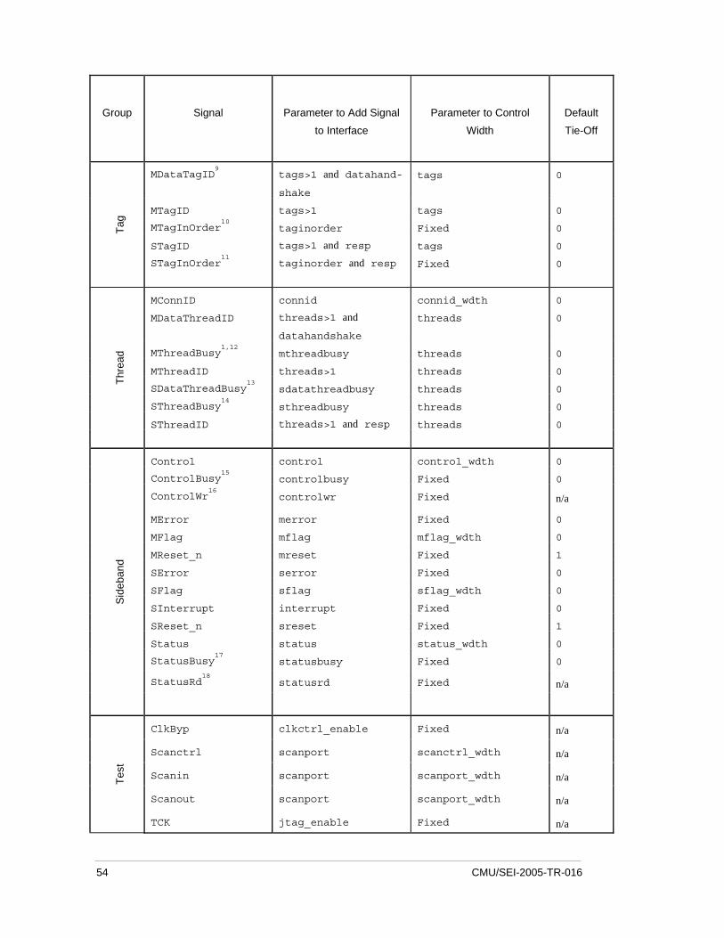
Group
Signal
Parameter to Add Signal
to Interface
Parameter to Control
Width
Default
Tie-Off
MDataTagID9
tags>1 and datahand-
shake
tags 0
MTagID tags>1 tags 0
MTagInOrder10
taginorder Fixed 0
STagID tags>1 and resp tags 0
STagInOrder11
taginorder and resp Fixed 0
Tag
MConnID connid connid_wdth 0
MDataThreadID threads>1 and
datahandshake
threads 0
MThreadBusy1,12
mthreadbusy threads 0
MThreadID threads>1 threads 0
SDataThreadBusy13
sdatathreadbusy threads 0
SThreadBusy14
sthreadbusy threads 0
SThreadID threads>1 and resp threads 0
Thre
ad
Control control control_wdth 0
ControlBusy15
controlbusy Fixed 0
ControlWr16
controlwr Fixed n/a
MError merror Fixed 0
MFlag mflag mflag_wdth 0
MReset_n mreset Fixed 1
SError serror Fixed 0
SFlag sflag sflag_wdth 0
SInterrupt interrupt Fixed 0
SReset_n sreset Fixed 1
Status status status_wdth 0
StatusBusy17
statusbusy Fixed 0
StatusRd18
statusrd Fixed n/a
Side
band
ClkByp clkctrl_enable Fixed n/a
Scanctrl scanport scanctrl_wdth n/a
Scanin scanport scanport_wdth n/a
Scanout scanport scanport_wdth n/a
Test
TCK jtag_enable Fixed n/a
54 CMU/SEI-2005-TR-016
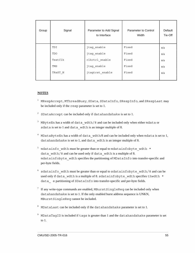
Group
Signal
Parameter to Add Signal
to Interface
Parameter to Control
Width
Default
Tie-Off
TDI jtag_enable Fixed n/a
TDO jtag_enable Fixed n/a
TestClk clkctrl_enable Fixed n/a
TMS jtag_enable Fixed n/a
TRsST_N jtagtrst_enable Fixed n/a
NOTES
1 MRespAccept, MThreadBusy, SData, SDataInfo, SRespInfo, and SRespLast may be included only if the resp parameter is set to 1.
2 SDataAccept can be included only if datahandshake is set to 1.
3 MByteEn has a width of data_wdth/8 and can be included only when either mdata or sdata is set to 1 and data_wdth is an integer multiple of 8.
4 MDataByteEn has a width of data_wdth/8 and can be included only when mdata is set to 1, datahandshake is set to 1, and data_wdth is an integer multiple of 8.
5 mdatainfo_wdth must be greater than or equal to mdatainfobyte_wdth * data_wdth/8 and can be used only if data_wdth is a multiple of 8. mdatainfobyte_wdth specifies the partitioning of MDataInfo into transfer-specific and per-byte fields.
6 sdatainfo_wdth must be greater than or equal to sdatainfobyte_wdth/8 and can be used only if data_wdth is a multiple of 8. sdatainfobyte_wdth specifies thwdth * data_ e partitioning of SDataInfo into transfer-specific and per-byte fields.
7 If any write-type commands are enabled, MBurstSingleReq can be included only when datahandshake is set to 1. If the only enabled burst address sequence is UNKN, MBurstSingleReq cannot be included.
8 MDataLast can be included only if the datahandshake parameter is set to 1.
9 MDataTagID is included if tags is greater than 1 and the datahandshake parameter is set to 1.
CMU/SEI-2005-TR-016 55
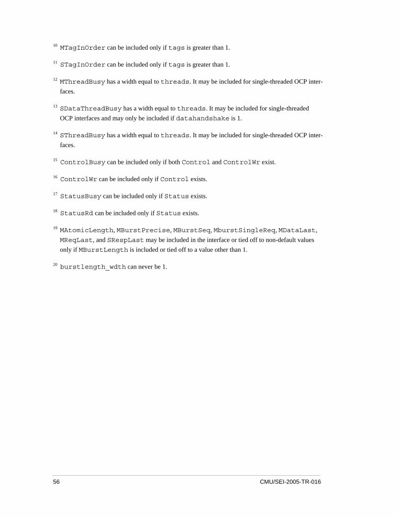
10 MTagInOrder can be included only if tags is greater than 1.
11 STagInOrder can be included only if tags is greater than 1.
12 MThreadBusy has a width equal to threads. It may be included for single-threaded OCP inter-faces.
13 SDataThreadBusy has a width equal to threads. It may be included for single-threaded OCP interfaces and may only be included if datahandshake is 1.
14 SThreadBusy has a width equal to threads. It may be included for single-threaded OCP inter-faces.
15 ControlBusy can be included only if both Control and ControlWr exist.
16 ControlWr can be included only if Control exists.
17 StatusBusy can be included only if Status exists.
18 StatusRd can be included only if Status exists.
19 MAtomicLength, MBurstPrecise, MBurstSeq, MburstSingleReq, MDataLast, MReqLast, and SRespLast may be included in the interface or tied off to non-default values only if MBurstLength is included or tied off to a value other than 1.
20 burstlength_wdth can never be 1.
56 CMU/SEI-2005-TR-016
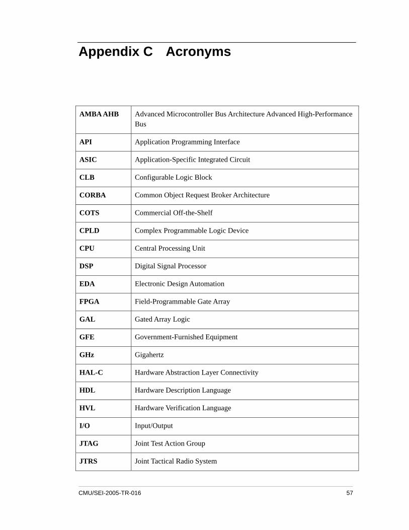
Appendix C Acronyms
AMBA AHB Advanced Microcontroller Bus Architecture Advanced High-Performance Bus
API Application Programming Interface
ASIC Application-Specific Integrated Circuit
CLB Configurable Logic Block
CORBA Common Object Request Broker Architecture
COTS Commercial Off-the-Shelf
CPLD Complex Programmable Logic Device
CPU Central Processing Unit
DSP Digital Signal Processor
EDA Electronic Design Automation
FPGA Field-Programmable Gate Array
GAL Gated Array Logic
GFE Government-Furnished Equipment
GHz Gigahertz
HAL-C Hardware Abstraction Layer Connectivity
HDL Hardware Description Language
HVL Hardware Verification Language
I/O Input/Output
JTAG Joint Test Action Group
JTRS Joint Tactical Radio System
CMU/SEI-2005-TR-016 57
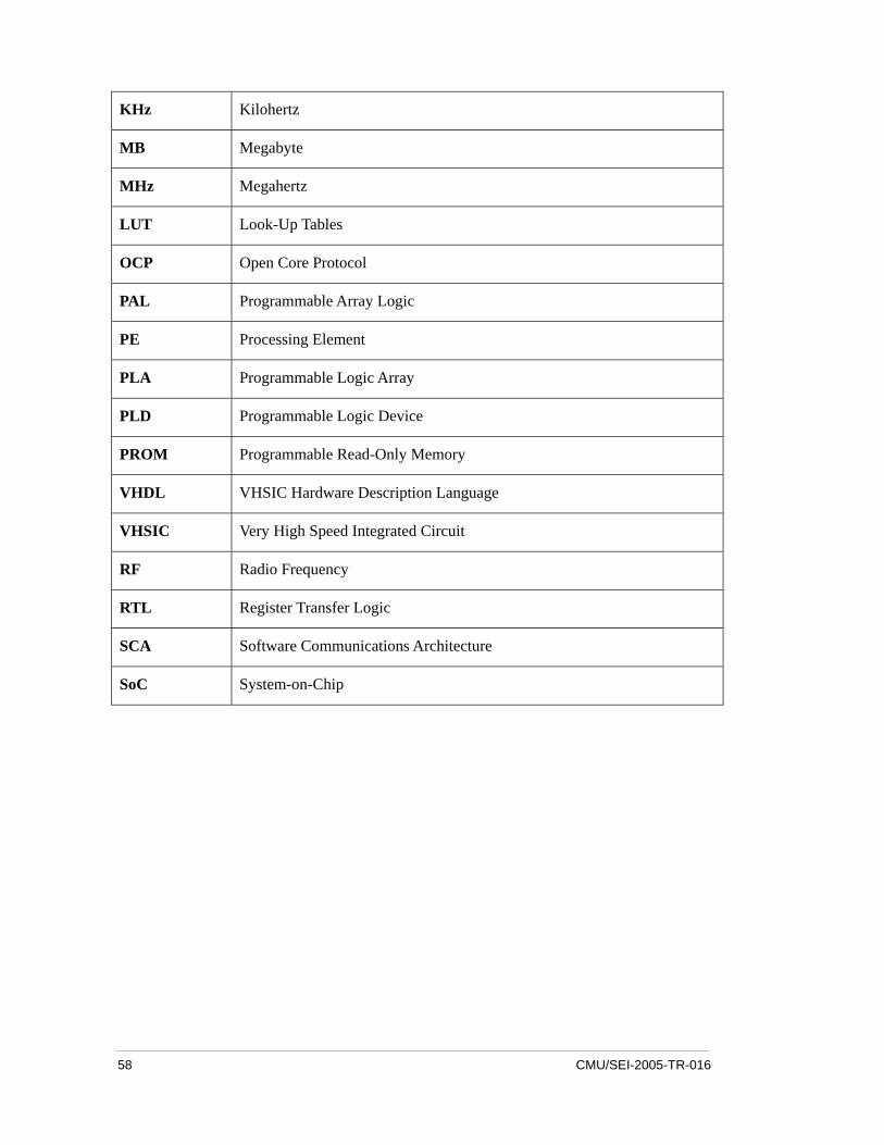
KHz Kilohertz
MB Megabyte
MHz Megahertz
LUT Look-Up Tables
OCP Open Core Protocol
PAL Programmable Array Logic
PE Processing Element
PLA Programmable Logic Array
PLD Programmable Logic Device
PROM Programmable Read-Only Memory
VHDL VHSIC Hardware Description Language
VHSIC Very High Speed Integrated Circuit
RF Radio Frequency
RTL Register Transfer Logic
SCA Software Communications Architecture
SoC System-on-Chip
58 CMU/SEI-2005-TR-016
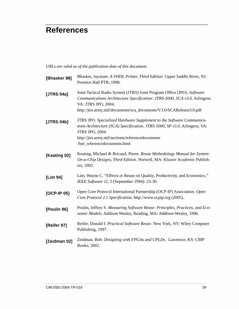
References
URLs are valid as of the publication date of this document.
[Bhasker 98] Bhasker, Jayaram. A VHDL Primer, Third Edition. Upper Saddle River, NJ: Prentice Hall PTR, 1998.
[JTRS 04a] Joint Tactical Radio System (JTRS) Joint Program Office (JPO). Software Communications Architecture Specification: JTRS-5000, SCA v3.0. Arlington, VA: JTRS JPO, 2004. http://jtrs.army.mil/documents/sca_documents/V3.0/SCARelease3.0.pdf
[JTRS 04b] JTRS JPO. Specialized Hardware Supplement to the Software Communica-tions Architecture (SCA) Specification: JTRS-5000, SP v3.0. Arlington, VA: JTRS JPO, 2004. http://jtrs.army.mil/sections/referencedocuments /fset_referencedocuments.html
[Keating 02] Keating, Michael & Bricaud, Pierre. Reuse Methodology Manual for System-On-a-Chip Designs, Third Edition. Norwell, MA: Kluwer Academic Publish-ers, 2002.
[Lim 94] Lim, Wayne C. “Effects or Reuse on Quality, Productivity, and Economics.” IEEE Software 11, 5 (September 1994): 23-30.
[OCP-IP 05] Open Core Protocol International Partnership (OCP-IP) Association. Open Core Protocol 2.1 Specification. http://www.ocpip.org (2005).
[Poulin 96] Poulin, Jeffrey S. Measuring Software Reuse: Principles, Practices, and Eco-nomic Models. Addison Wesley, Reading, MA: Addison-Wesley, 1996.
[Reifer 97] Reifer, Donald J. Practical Software Reuse. New York, NY: Wiley Computer Publishing, 1997.
[Zeidman 02] Zeidman, Bob. Designing with FPGAs and CPLDs. Lawrence, KS: CMP Books, 2002.
CMU/SEI-2005-TR-016 59

60 CMU/SEI-2005-TR-016
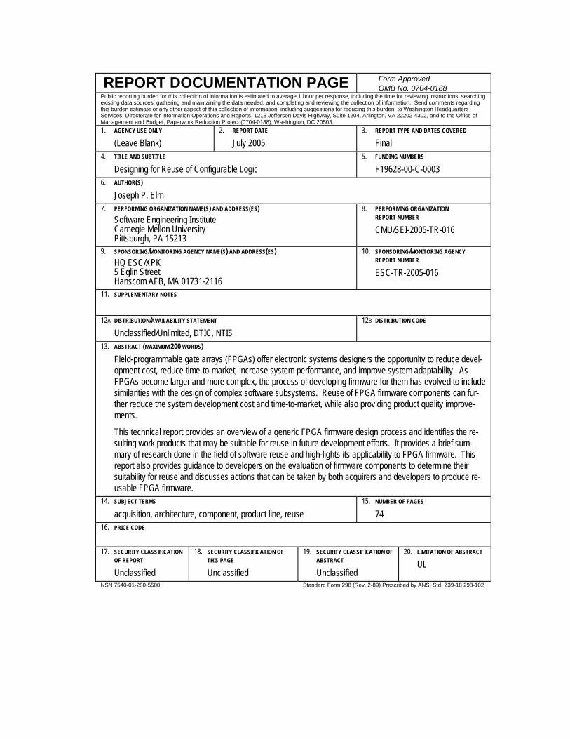
REPORT DOCUMENTATION PAGE Form Approved
OMB No. 0704-0188 Public reporting burden for this collection of information is estimated to average 1 hour per response, including the time for reviewing instructions, searching existing data sources, gathering and maintaining the data needed, and completing and reviewing the collection of information. Send comments regarding this burden estimate or any other aspect of this collection of information, including suggestions for reducing this burden, to Washington Headquarters Services, Directorate for information Operations and Reports, 1215 Jefferson Davis Highway, Suite 1204, Arlington, VA 22202-4302, and to the Office of Management and Budget, Paperwork Reduction Project (0704-0188), Washington, DC 20503. 1. AGENCY USE ONLY
(Leave Blank) 2. REPORT DATE
July 2005 3. REPORT TYPE AND DATES COVERED
Final 4. TITLE AND SUBTITLE
Designing for Reuse of Configurable Logic 5. FUNDING NUMBERS
F19628-00-C-0003 6. AUTHOR(S)
Joseph P. Elm 7. PERFORMING ORGANIZATION NAME(S) AND ADDRESS(ES)
Software Engineering Institute Carnegie Mellon University Pittsburgh, PA 15213
8. PERFORMING ORGANIZATION REPORT NUMBER
CMU/SEI-2005-TR-016
9. SPONSORING/MONITORING AGENCY NAME(S) AND ADDRESS(ES) HQ ESC/XPK 5 Eglin Street Hanscom AFB, MA 01731-2116
10. SPONSORING/MONITORING AGENCY REPORT NUMBER
ESC-TR-2005-016
11. SUPPLEMENTARY NOTES
12A DISTRIBUTION/AVAILABILITY STATEMENT
Unclassified/Unlimited, DTIC, NTIS 12B DISTRIBUTION CODE
13. ABSTRACT (MAXIMUM 200 WORDS)
Field-programmable gate arrays (FPGAs) offer electronic systems designers the opportunity to reduce devel-opment cost, reduce time-to-market, increase system performance, and improve system adaptability. As FPGAs become larger and more complex, the process of developing firmware for them has evolved to include similarities with the design of complex software subsystems. Reuse of FPGA firmware components can fur-ther reduce the system development cost and time-to-market, while also providing product quality improve-ments.
This technical report provides an overview of a generic FPGA firmware design process and identifies the re-sulting work products that may be suitable for reuse in future development efforts. It provides a brief sum-mary of research done in the field of software reuse and high-lights its applicability to FPGA firmware. This report also provides guidance to developers on the evaluation of firmware components to determine their suitability for reuse and discusses actions that can be taken by both acquirers and developers to produce re-usable FPGA firmware.
14. SUBJECT TERMS
acquisition, architecture, component, product line, reuse 15. NUMBER OF PAGES
74 16. PRICE CODE
17. SECURITY CLASSIFICATION
OF REPORT
Unclassified
18. SECURITY CLASSIFICATION OF THIS PAGE
Unclassified
19. SECURITY CLASSIFICATION OF ABSTRACT
Unclassified
20. LIMITATION OF ABSTRACT
UL
NSN 7540-01-280-5500 Standard Form 298 (Rev. 2-89) Prescribed by ANSI Std. Z39-18 298-102


![MPC8548E Configurable Development System … Configurable Development System Reference Manual, ... [4:0] ... MPC8548E Configurable Development System Reference Manual,](https://img.pdfslide.us/doc/110x75/5af028337f8b9ac62b8e4c0e/mpc8548e-configurable-development-system-configurable-development-system-reference.jpg)