Embed Size (px)
Citation preview
University of Arkansas, Fayetteville University of Arkansas, Fayetteville
ScholarWorks@UARK ScholarWorks@UARK
Graduate Theses and Dissertations
5-2014
Designing Customizable Network-on-Chip with support for Designing Customizable Network-on-Chip with support for
Embedded Private Memory for Multi-Processor System-on-Chips Embedded Private Memory for Multi-Processor System-on-Chips
Azad Fakhari University of Arkansas, Fayetteville
Follow this and additional works at: https://scholarworks.uark.edu/etd
Part of the Computer and Systems Architecture Commons
Citation Citation Fakhari, A. (2014). Designing Customizable Network-on-Chip with support for Embedded Private Memory for Multi-Processor System-on-Chips. Graduate Theses and Dissertations Retrieved from https://scholarworks.uark.edu/etd/1058
This Thesis is brought to you for free and open access by ScholarWorks@UARK. It has been accepted for inclusion in Graduate Theses and Dissertations by an authorized administrator of ScholarWorks@UARK. For more information, please contact [email protected].

Designing Customizable Network-on-Chipwith support for Embedded Private Memory
for Multi-Processor System-on-Chips
Designing Customizable Network-on-Chipwith support for Embedded Private Memory
for Multi-Processor System-on-Chips
A thesis submitted in partial fulfillmentof the requirements for the degree of
Master of Science in Computer Engineering
By
Azad FakhariIran University of Science and Technology
Bachelor of Science in Computer Hardware Engineering, 2009
May 2014University of Arkansas
This thesis is approved for recommendation to the Graduate Council
—————————————————-Dr. David Andrews, Ph.D.Thesis Director
—————————————————-Dr. Christophe Bobda, Ph.D.Committee Member
—————————————————-Dr. Jia Di, Ph.D.Committee Member
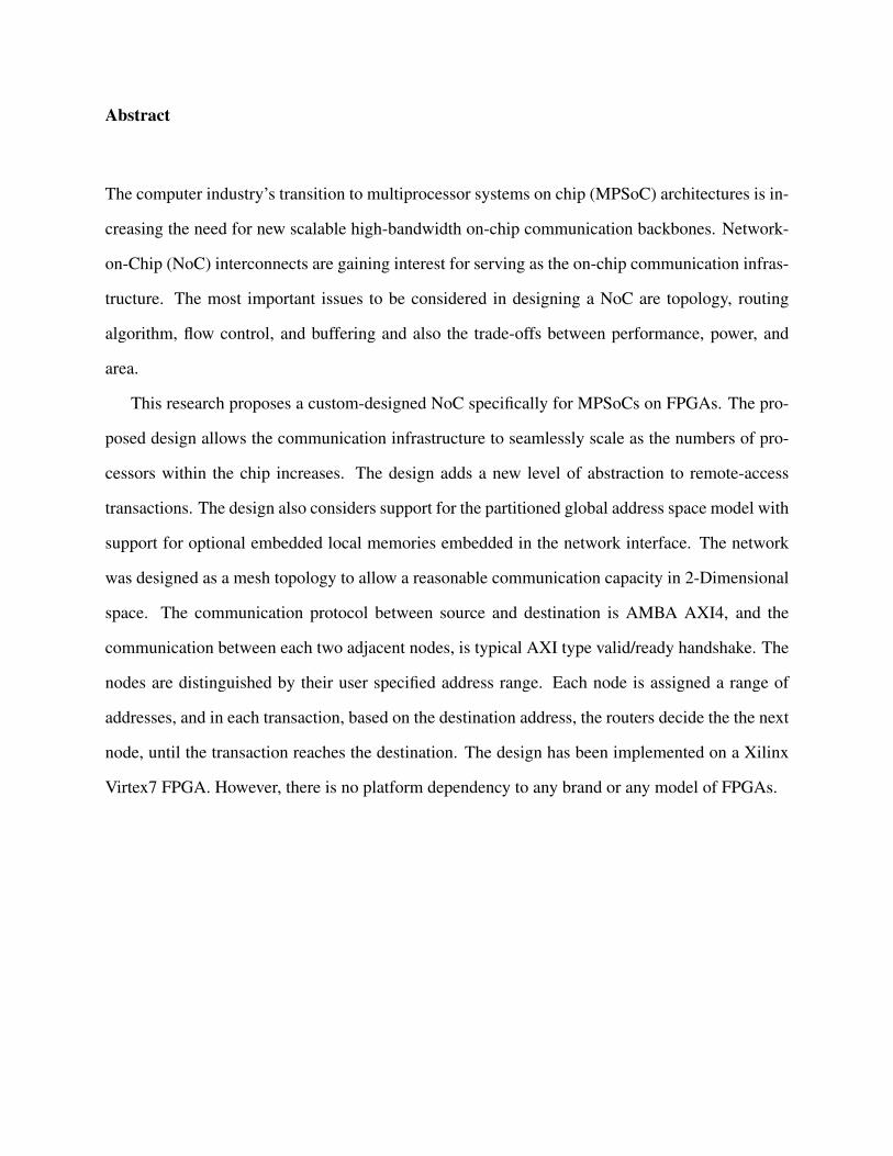
Abstract
The computer industry’s transition to multiprocessor systems on chip (MPSoC) architectures is in-
creasing the need for new scalable high-bandwidth on-chip communication backbones. Network-
on-Chip (NoC) interconnects are gaining interest for serving as the on-chip communication infras-
tructure. The most important issues to be considered in designing a NoC are topology, routing
algorithm, flow control, and buffering and also the trade-offs between performance, power, and
area.
This research proposes a custom-designed NoC specifically for MPSoCs on FPGAs. The pro-
posed design allows the communication infrastructure to seamlessly scale as the numbers of pro-
cessors within the chip increases. The design adds a new level of abstraction to remote-access
transactions. The design also considers support for the partitioned global address space model with
support for optional embedded local memories embedded in the network interface. The network
was designed as a mesh topology to allow a reasonable communication capacity in 2-Dimensional
space. The communication protocol between source and destination is AMBA AXI4, and the
communication between each two adjacent nodes, is typical AXI type valid/ready handshake. The
nodes are distinguished by their user specified address range. Each node is assigned a range of
addresses, and in each transaction, based on the destination address, the routers decide the the next
node, until the transaction reaches the destination. The design has been implemented on a Xilinx
Virtex7 FPGA. However, there is no platform dependency to any brand or any model of FPGAs.

Acknowledgment
I would like to thank my adviser and my mentor Dr. David Andrews for giving me the opportunity
to work in his research laboratory and for his support and guidance throughout my Master’s pro-
gram. I would also like to thank Dr. Ken Eguro, from whom I have learned a tremendous amount
during my time in Microsoft Research. Additionally, I would like to thank my thesis committee,
Dr. Chrisophe Bobda and Dr. Jia Di, for broadening my knowledge in this field. Finally, I would
like to thank my labmates in the CSDL lab for their friendship and support.
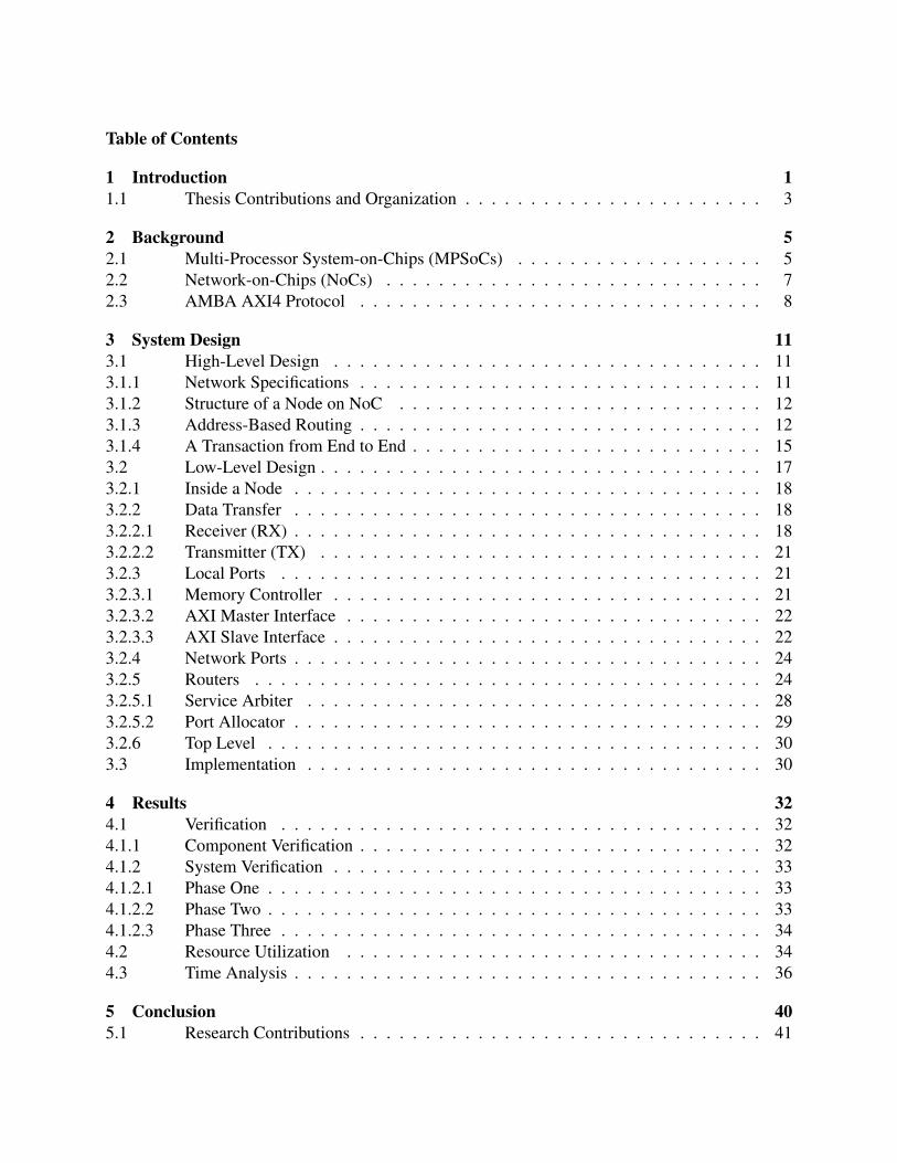
Table of Contents
1 Introduction 11.1 Thesis Contributions and Organization . . . . . . . . . . . . . . . . . . . . . . . 3
2 Background 52.1 Multi-Processor System-on-Chips (MPSoCs) . . . . . . . . . . . . . . . . . . . 52.2 Network-on-Chips (NoCs) . . . . . . . . . . . . . . . . . . . . . . . . . . . . . 72.3 AMBA AXI4 Protocol . . . . . . . . . . . . . . . . . . . . . . . . . . . . . . . 8
3 System Design 113.1 High-Level Design . . . . . . . . . . . . . . . . . . . . . . . . . . . . . . . . . 113.1.1 Network Specifications . . . . . . . . . . . . . . . . . . . . . . . . . . . . . . . 113.1.2 Structure of a Node on NoC . . . . . . . . . . . . . . . . . . . . . . . . . . . . 123.1.3 Address-Based Routing . . . . . . . . . . . . . . . . . . . . . . . . . . . . . . . 123.1.4 A Transaction from End to End . . . . . . . . . . . . . . . . . . . . . . . . . . . 153.2 Low-Level Design . . . . . . . . . . . . . . . . . . . . . . . . . . . . . . . . . . 173.2.1 Inside a Node . . . . . . . . . . . . . . . . . . . . . . . . . . . . . . . . . . . . 183.2.2 Data Transfer . . . . . . . . . . . . . . . . . . . . . . . . . . . . . . . . . . . . 183.2.2.1 Receiver (RX) . . . . . . . . . . . . . . . . . . . . . . . . . . . . . . . . . . . . 183.2.2.2 Transmitter (TX) . . . . . . . . . . . . . . . . . . . . . . . . . . . . . . . . . . 213.2.3 Local Ports . . . . . . . . . . . . . . . . . . . . . . . . . . . . . . . . . . . . . 213.2.3.1 Memory Controller . . . . . . . . . . . . . . . . . . . . . . . . . . . . . . . . . 213.2.3.2 AXI Master Interface . . . . . . . . . . . . . . . . . . . . . . . . . . . . . . . . 223.2.3.3 AXI Slave Interface . . . . . . . . . . . . . . . . . . . . . . . . . . . . . . . . . 223.2.4 Network Ports . . . . . . . . . . . . . . . . . . . . . . . . . . . . . . . . . . . . 243.2.5 Routers . . . . . . . . . . . . . . . . . . . . . . . . . . . . . . . . . . . . . . . 243.2.5.1 Service Arbiter . . . . . . . . . . . . . . . . . . . . . . . . . . . . . . . . . . . 283.2.5.2 Port Allocator . . . . . . . . . . . . . . . . . . . . . . . . . . . . . . . . . . . . 293.2.6 Top Level . . . . . . . . . . . . . . . . . . . . . . . . . . . . . . . . . . . . . . 303.3 Implementation . . . . . . . . . . . . . . . . . . . . . . . . . . . . . . . . . . . 30
4 Results 324.1 Verification . . . . . . . . . . . . . . . . . . . . . . . . . . . . . . . . . . . . . 324.1.1 Component Verification . . . . . . . . . . . . . . . . . . . . . . . . . . . . . . . 324.1.2 System Verification . . . . . . . . . . . . . . . . . . . . . . . . . . . . . . . . . 334.1.2.1 Phase One . . . . . . . . . . . . . . . . . . . . . . . . . . . . . . . . . . . . . . 334.1.2.2 Phase Two . . . . . . . . . . . . . . . . . . . . . . . . . . . . . . . . . . . . . . 334.1.2.3 Phase Three . . . . . . . . . . . . . . . . . . . . . . . . . . . . . . . . . . . . . 344.2 Resource Utilization . . . . . . . . . . . . . . . . . . . . . . . . . . . . . . . . 344.3 Time Analysis . . . . . . . . . . . . . . . . . . . . . . . . . . . . . . . . . . . . 36
5 Conclusion 405.1 Research Contributions . . . . . . . . . . . . . . . . . . . . . . . . . . . . . . . 41

5.2 Future Work . . . . . . . . . . . . . . . . . . . . . . . . . . . . . . . . . . . . . 42
References 43

List of Figures
2.1 Channel architecture of reads[5] . . . . . . . . . . . . . . . . . . . . . . . . . . . . . 9
2.2 Channel architecture of writes[5] . . . . . . . . . . . . . . . . . . . . . . . . . . . . . 10
3.1 Structure of a node from outside . . . . . . . . . . . . . . . . . . . . . . . . . . . . . 13
3.2 Connections between the nodes . . . . . . . . . . . . . . . . . . . . . . . . . . . . . . 14
3.3 Address ranges in a 4x4 mesh . . . . . . . . . . . . . . . . . . . . . . . . . . . . . . 16
3.4 Inside of a node . . . . . . . . . . . . . . . . . . . . . . . . . . . . . . . . . . . . . . 19
3.5 Receiver state machine . . . . . . . . . . . . . . . . . . . . . . . . . . . . . . . . . . 20
3.6 Receiver Module . . . . . . . . . . . . . . . . . . . . . . . . . . . . . . . . . . . . . 21
3.7 The local port and the memory controller . . . . . . . . . . . . . . . . . . . . . . . . 23
3.8 The structure of the router . . . . . . . . . . . . . . . . . . . . . . . . . . . . . . . . 28
4.1 The resource utilization for different sizes of mesh . . . . . . . . . . . . . . . . . . . 35
4.2 Latency with and without interfering traffic . . . . . . . . . . . . . . . . . . . . . . . 38
List of Tables
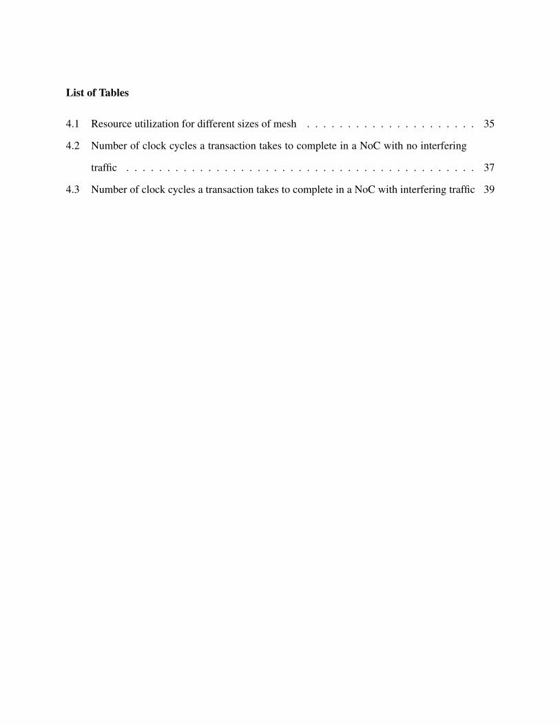
4.1 Resource utilization for different sizes of mesh . . . . . . . . . . . . . . . . . . . . . 35
4.2 Number of clock cycles a transaction takes to complete in a NoC with no interfering
traffic . . . . . . . . . . . . . . . . . . . . . . . . . . . . . . . . . . . . . . . . . . . 37
4.3 Number of clock cycles a transaction takes to complete in a NoC with interfering traffic 39
Terms and Definitions
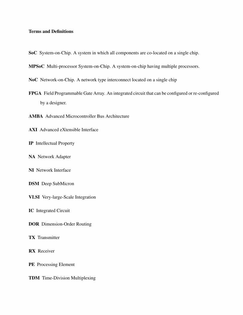
SoC System-on-Chip. A system in which all components are co-located on a single chip.
MPSoC Multi-processor System-on-Chip. A system-on-chip having multiple processors.
NoC Network-on-Chip. A network type interconnect located on a single chip
FPGA Field Programmable Gate Array. An integrated circuit that can be configured or re-configured
by a designer.
AMBA Advanced Microcontroller Bus Architecture
AXI Advanced eXtensible Interface
IP Intellectual Property
NA Network Adapter
NI Network Interface
DSM Deep SubMicron
VLSI Very-large-Scale Integration
IC Integrated Circuit
DOR Dimension-Order Routing
TX Transmitter
RX Receiver
PE Processing Element
TDM Time-Division Multiplexing

VC Virtual Channel
NF Negative First. Routing algorithm
WF West First. Routing algorithm
VHDL VHSIC Hardware Description Language
CRT Constrained Random Testing
Tcl Tool Command Language
RAM Random-Access Memory
LUT Lookup Table. A digital building block used to implement N-bit binary functions via lookup
operations.
DMA Direct Memory Access. Often referring to hardware devices that can perform memory-to-
memory operations without processor assistance.
Chapter 1
Introduction
Commercial Systems-on-Chip (SoC) designs continue to be dominated by shared-medium bus-
based functional interconnects for integrating IP blocks. The continued adherence to bus base
interconnects is in part historical due to their wide spread availability, ease of use, and familiarity.
Pragmatically bus interconnects still remain relevant for today’s multiprocessor SoC (MPSoC)
systems that contain relatively few processors. However the number of processors and IP modules
that will be integrated into future MPSoCs is projected to follow Moore’s law with a doubling of
IP modules every 18 months. The commercial MPSoC industry will soon be forced to deal with
the inevitable; bus-based interconnection architectures will prevent these systems from delivering
the performance that will be required by next generation applications[18][20].
A fundamental question that SoC manufacturers face is determining what type of interconnect
structure should replace standard buses. Many types of different structures have been proposed
as replacement interconnects for global bus structures for next generation MPSoPCs[39]. Hierar-
chical bus structures are a natural evolution of global buses. While hierarchical buses have some
performance advantages over a single bus, their resource requirements and performance will pre-
vent them from scaling to large numbers of processors. They are also limited in their ability to
support custom communications patterns. Recently Intel included a ring bus architecture within
their Knights corner manycore chip. Ring buses provide better scalability than hierarchical or
distributed buses but introduce variable latencies that can effect performance.
Of the different interconnect structures being studied Network on Chip (NoC) structures have
continued to enjoy growing interest in the academic community. This interest is primarily based
on the NoC’s ability to provide performance that scales with the number of processors. In general,
a network-on-chip can be viewed as being composed of three main building blocks. The first block
contains the links that physically connect the nodes and implements the communication. The
1
second block is the router, which implements the communication protocol. The router receives
packets from the shared links and, according to the address information contained in each packet,
forwards the packet to the client attached to it or onto another shared link. The protocol itself
consists of a set of policies defined during the design (and implemented within the router) to
handle common situations that can occur during the transmission of a packet. Policies include how
to process two or more packets arriving at the same time, for a single channel, avoiding deadlock
and livelock situations, reducing the communication latency. The last building block is the network
adapter (NA) or network interface (NI). This block makes the logic connection between the IP cores
and the network.
While NoCs do hold promise, there are still several issues must be explored to understand if
NoCs will be able to serve as the interconnect structures for next generation FPGA based MPSoCs.
Addressing the following issues was the main motivation for this work.
Issue 1: Support for local memory: Most multi-processor systems use some type of local mem-
ory for the PEs. The local memory can be placed in the main interconnect infrastructure where it is
accessible by the PE, or a secondary light-weight interconnect can be used for the communication
between each PE and its local memory. Consequently, having a smart support for local memory in
the interconnect backbone of the MPSoCs reduces the overhead of handling the local memory.
Issue 2: Unification of transactions: In MPSoC systems, based on the type of local resources
and the outside resources accessible to the PE, the type of transactions to access different resources
may vary. Unifying the transactions regardless of their locality ore remoteness reduces the over-
head of generating the transactions in each PE.
Issue 3: Customization of the NoC for each client: In heterogeneous systems, different clients
on the interconnect may require different services. For instance a PE may act as both master and
slave while a component such as memory controller always acts as slave. Also different PEs may
require local memories in different sizes. Customization of the NoC for each client allows the2
system to use the resources more efficiently.
This thesis attempts to explore these issues for FPGA Multiprocessor Systems on Chip com-
ponents.
1.1 Thesis Contributions and Organization
The thesis of this work is that Network-on-Chip interconnects can meet the communica-
tion needs while providing specific services for multi-processor systems. Those services
include support for local memory, transparency of the locality or the remoteness of the
accesses, and customization of each node based on the requirements of its client. These
services reduce the overhead of transaction generation on the PEs.
To explore this thesis statement, this thesis provides the following set of contributions:
• A working implementation of a prototype NoC on an FPGA. The NoC is a scalable, reliable,
and customizable infrastructure that uses an existing well-known communication protocol,
AMBA AXI, as its network interface. This allows the basic NoC to be portable. An im-
portant attribute of the proposed NoC is its support of a partitioned global address space
memory model to support scalability. The design supports inclusion of embedded local
memory in each node, which is accessible both locally and remotely. This allows all trans-
actions, whether local or remote to go through the same serving process. This is important
support for the partitioned global address space memory model as it enables the locality or
remoteness of the transaction to be transparent from the connected node.
• A complete implementation of both master side and slave sides of the AMBA AXI protocol
to interface with the NoC
• The design, implementation, and optimization of a scheduler (service arbiter) to prevent the
system from possible congestion.
3

• The design of a complex memory controller to synchronize remote and local accesses as
well as read and write accesses.
• The design of an address compilation mechanism that maps the location of each node in the
mesh to an address range, and decodes every address to its relative destination location in
the matrix of nodes.
• A tool that automates the generation of the top level architecture. The tool customizes the
size of the mesh, the type of the nodes(master/slave/both), and their need for memory con-
troller.
• An automated simulation process that generates the large number of signals in the system,
This eliminates the need for system designers to engage in time consuming manual simula-
tion and ordering of waveforms to observe signals.
This thesis takes a close look inside the network and describes different parts both at func-
tional level and the architectural level. Chapter 2 provides some background information on Multi-
Processor System-on-Chips as well as Network-on-chips. Details of the AMBA AXI protocol used
in this work is also described. Chapter 2 first observes the system at functional level as a network
and then explains the design details of every component inside the system. This is followed by
detailed discussions of the implementation of the design on the FPGA. Chapter 4 describes the
verification process used to test and evaluate the NoC and presents experimental results. Finally,
chapter 5 provides conclusions and directions for future work.
4
Chapter 2
Background
2.1 Multi-Processor System-on-Chips (MPSoCs)
The main motivation for the developments during decades is the System-on-Chip (SoC) technolo-
gies, where that complex applications are integrated onto single chips. These products such as
mobile phones, notebooks and personal hand-held sets are also becoming faster, smaller-in-size,
larger-in-capacity, lighter-in- weight, lower-in-power-consumption and cheaper. Following this
trend, more applications and even systems could be integrated onto a single chip. However, the
conventional methodologies for SoC design and integration do not evenly advance due to the big
challenges confronted.
Deep SubMicron (DSM) effects[16][29][45]: In early days of VLSI design, signal integrity
effects such as interconnect delay, crosstalk, inter-symbol interference, substrate coupling, transmission-
line effects, etc. were negligible due to slow clock speed and low integration density. Interconnec-
tion was reliable and robust. For 250 nm (with aluminum) and 180 nm (with copper) and below,
the dominating factor for chip robustness and performance became the interconnect. The speed
and the reliability of the wires are not keeping up with the increasing pace of the transistor density.
More noise sources due to inductive fringing, crosstalk and transmission line effects are coupled to
other circuit nodes globally on the chip via the substrate, common return ground and electromag-
netic interference. The increasing use of high-speed circuit families, for example, domino circuitry,
scaling of power supply and threshold voltages, and mixed-signal integration combine to make the
chips more noise-sensitive. Third, higher device densities and faster switching frequencies cause
larger switching-currents to flow in the power and ground networks. Consequently, power supply
is plagued with excessive IR voltage drops as well as inductive voltage drops over the power dis-
tribution network and package pins. Power supply noise degrades not only the driving capability
of gates but also causes possible false switching of logical gates. Today signal and power integrity5

analysis is as important as timing, area and power analysis.
Global Synchrony[2][21]: Predominating digital IC designs have been following a globally
synchronous design style where a global clock tree is distributed on the chip, and logic blocks
function synchronously. This style is unlikely to survive with future wire interconnect because
technology scaling does not treat wire delay and gate delay equally. While gate delay has been
getting dramatically smaller in proportion to the gate length, wires have slowed down. As the
chip s become communication-bound, multiple cycles are required to transmit a signal across their
diameter. Moreover, a clock tree is consuming larger portions of power and area budget and clock
skew is claiming an ever larger portion of the total cycle time. Even if an unlimited number of
transistors are available on a chip, chip design is to be constrained by communication rather than
capacity.
Communication Architecture[7][12]: Most SoCs have a bus-based architecture, such as sim-
ple, hierarchical or crossbar-type buses. In contrast to the scaling of chip capacity, buses do not
scale well with the system size in terms of bandwidth, clocking frequency and power. First, a bus
system has very limited concurrent communication capability since only one device can drive a
bus segment at a time. Second, as the number of clients grows, the intrinsic resistance and capac-
itance of the bus also increase. This means that the bus speed is inherently difficult to scale up.
Third, a bus is inefficient in energy since every data transfer is broadcast. The entire bus wire has
to be switched on and off. This means that the data must reach each receiver at great energy cost.
Although improvements such as split-transaction protocols and advanced arbitration schemes for
buses have been proposed, these incremental techniques can not overcome the fundamental prob-
lems.
Power and Thermal Management[32][38]: As circuits run with higher and higher frequen-
cies, lowering power consumption is becoming extremely important. Power is a design constraint,
which is no more subordinate to performance. Despite process and circuit improvements, power
consumption shows rapid growth. In face of DSM effects, reducing power consumption is becom-
ing even more challenging. As devices shrink to sub-micron dimensions, the supply voltage must
6

be reduced to avoid damaging electric fields. This development, in turn, requires a reduced thresh-
old voltage. However, leakage current increases exponentially with a decrease in the threshold
voltage. Further, leakage occurs as long as power flows through the circuit. This constant current
can produce an increase in the chip temperature, which in turn causes an increase in the thermal
voltage, leading to a further increase in leakage current.
Verification[36][11]: Today SoC design teams are struggling with the complexity of multimil-
lion gate designs. System verification runs through the whole design process from specification
to implementation, typically with formal methods or simulation-based validation. As the system
has become extremely complex, the verification or validation consumes an increasing portion of
the product development time. The verification effort has reached as high as 70% of engineering
efforts.
Productivity Gap[4][11]: Simply put, productivity gap is the gap between what we are capable
of building and what we are capable of designing. In line with Moores law, the logic capacity of a
single chip has increased at the rate of 58% per annum compounded. The complexity of developing
SoCs is increasing continuously in order to exploit the potential of the chip capacity. However, the
productivity of hardware and software design is not growing at a comparable pace. The hardware
design productivity is increased at a rate in the range 20% to 25% per annum compounded. Even
worse, the software design productivity improves at a rate in the range from 8% to 10% per annum
compounded. As a consequence, the costs of developing advanced SoCs are increasing at an
alarming pace and time-to-market is negatively affected. The design team size is increased by
more than 20% per year. This huge investment is becoming a serious threshold for new product
developments and is slowing down the innovation in the semiconductor industry [27]
2.2 Network-on-Chips (NoCs)
Integrating a large number of components onto a chip is becoming a major performance issue in
System-on-Chip (SoC) architectures [19][22][13][8]. Network-on-Chip (NoC) has been consid-
ered as a solution to address the communication demands of multi-core SoC architectures, due7
to scalability and parallelism in communication infrastructure [13][8]. Also, [34] talks about the
design trade-offs in NoC design and the performance evaluation based on different factors of the
design.
In projects such as CLICHE [15], Nostrum[31], and XGFT[24], new architectures have been
proposed to design NoC for multi-processor systems. In some other projects, NoCs have been de-
signed for specific purposes. For instance, in SoCWire [33] the network is designed to be optimized
for space application and GALS [41], targets inter-domain communication in heterogeneous DPS
platforms. DyNoC[28] has proposed runtime scheduling and resource allocation in the network to
increase the performance as well as flexibility. The NoC described in [14] is designed to ease the
use of memory in the NoC which is very similar to the proposed design in this thesis. Other works
such as [25] focus more on the power issues of the network. Projects such as [9] take advantage of
the more novel chip design technologies such as three-dimensional integrated circuits.
Some projects have focused on more specific aspects of Network-on-chip. For instance, vir-
tual channel allocation[40], deadlock free routing[23] and[17], coherency[26], dynamic priority
arbitration[43], and congestion control[3] are some of those areas. There are also other projects
that focus more on performance analysis [37][6][30]. Projects such as DART[42] and TOPAZ[1]
have worked on simulation of the NoC. Among all, CONNECT[35] has provided web-based front-
end to design user-customized NoCs for FPGAs.
2.3 AMBA AXI4 Protocol
The AMBA AXI is a high-performance communication protocol suitable for high-bandwidth high-
frequency systems. This protocol provides flexibility and efficiency in designing interconnection
and memory controllers by separating address, control, and data phases and also separating read
and write channels as well as supporting burst-based transactions. There are 5 separate channels
in AXI protocol
• Read Address (AR)
8
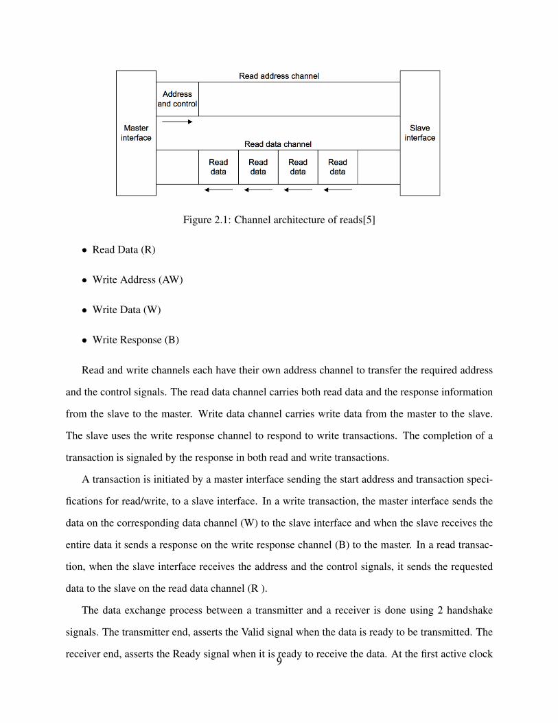
Figure 2.1: Channel architecture of reads[5]
• Read Data (R)
• Write Address (AW)
• Write Data (W)
• Write Response (B)
Read and write channels each have their own address channel to transfer the required address
and the control signals. The read data channel carries both read data and the response information
from the slave to the master. Write data channel carries write data from the master to the slave.
The slave uses the write response channel to respond to write transactions. The completion of a
transaction is signaled by the response in both read and write transactions.
A transaction is initiated by a master interface sending the start address and transaction speci-
fications for read/write, to a slave interface. In a write transaction, the master interface sends the
data on the corresponding data channel (W) to the slave interface and when the slave receives the
entire data it sends a response on the write response channel (B) to the master. In a read transac-
tion, when the slave interface receives the address and the control signals, it sends the requested
data to the slave on the read data channel (R ).
The data exchange process between a transmitter and a receiver is done using 2 handshake
signals. The transmitter end, asserts the Valid signal when the data is ready to be transmitted. The
receiver end, asserts the Ready signal when it is ready to receive the data. At the first active clock9
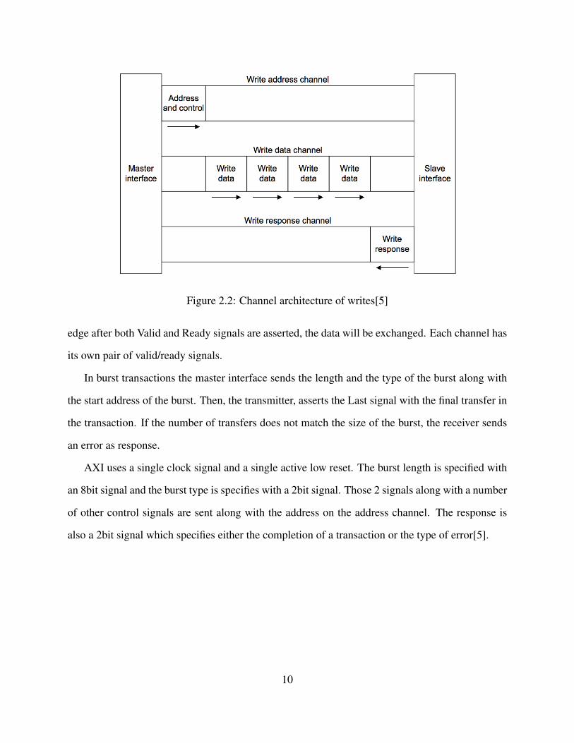
Figure 2.2: Channel architecture of writes[5]
edge after both Valid and Ready signals are asserted, the data will be exchanged. Each channel has
its own pair of valid/ready signals.
In burst transactions the master interface sends the length and the type of the burst along with
the start address of the burst. Then, the transmitter, asserts the Last signal with the final transfer in
the transaction. If the number of transfers does not match the size of the burst, the receiver sends
an error as response.
AXI uses a single clock signal and a single active low reset. The burst length is specified with
an 8bit signal and the burst type is specifies with a 2bit signal. Those 2 signals along with a number
of other control signals are sent along with the address on the address channel. The response is
also a 2bit signal which specifies either the completion of a transaction or the type of error[5].
10
Chapter 3
System Design
In this chapter, the design specification of the system is discussed by first looking at the high level
design and the details of the functions it provides. Then a view of the inside of the design is
provided to find out how each component works. Finally, the details of the implementation of the
design is discussed.
3.1 High-Level Design
In this section we look at the specifications of the network as a whole, and the details of the com-
munication from a high level perspective. We also track a transaction from source to destination to
understand the function of the network.
3.1.1 Network Specifications
Every network can be characterized by 3 major factors. First, there is the topology of the network
and the geometrical specifications of the nodes. The topology defines the spatial coordination
of the network. Then there is the flow control which handles the movement of the data from
source to destination. Finally, there is the routing mechanism which is responsible for finding
the path from source to destination through the network. This network is designed as a mesh to
function efficiently in the 2-dimensional space of the FPGA chip. The flow control is done by doing
valid/ready handshake between each two nodes on the path from the source to the destination.
The routing mechanism is adaptive and it is an adjusted Dimension-Order Routing (DOR) which
changes the order based on the traffic.
11
3.1.2 Structure of a Node on NoC
Each node in this NoC has 5 sets of ports. There is a set of ports for each possible direction in the
mech, plus a local port which is the network interface for the connected component. The directions
are entitled:
• North Port (N)
• East Port (E)
• South Port (S)
• West Port (W)
• Local Port (L)
Each set of ports includes a master subset and a slave subset. Each subset, consists of 5 separate
channels for each of the AXI channels. Figure 3.1 illustrates the structure of the node as a block.
The way each node is connected to the neighbor nodes is each master channel is connected to
the corresponding slave channel of the adjacent node, as it can be seen in figure 3.2 . For instance,
considering the horizontal connection between 2 adjacent nodes, the master AW east port of the
node on the left is connected to the slave AW west port of the node on the right. The same way for
the vertical connection, the slave B south port of the upper node is connected to the master B north
port of the lower node.
For each transmitter on a master channel, there is a receiver on the slave side for the same
channel, and for each transmitter on a slave channel, there is a receiver on the master side for the
same channel. Therefore, master sides of the channels are connected with the slave sides of the
channels channels of all the adjacent nodes and vice versa.
3.1.3 Address-Based Routing
In this design, the entire address range has been divided between the nodes. For instance, assuming
a 2x2 mesh, and 32bit address, the first node is assigned to the address range between 0x0000000012
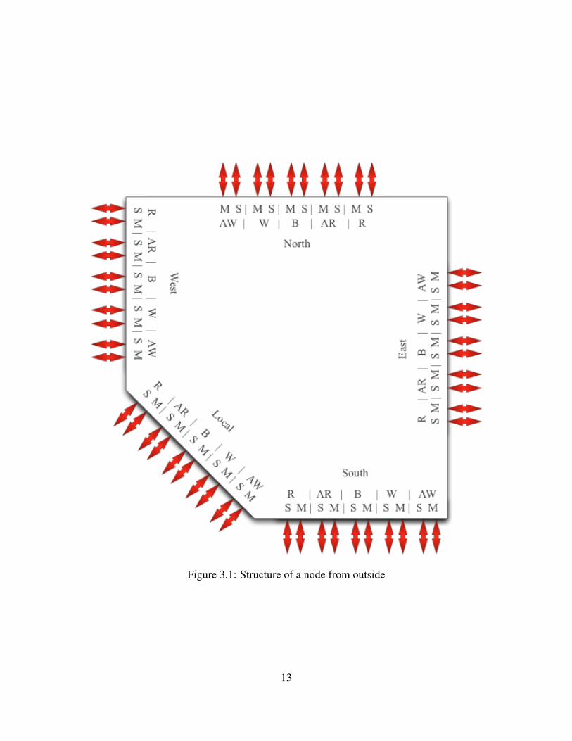
Figure 3.1: Structure of a node from outside
13
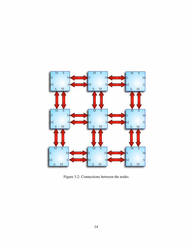
Figure 3.2: Connections between the nodes
14

and 0x3FFFFFFF, the second node between, 0x40000000 and 0x7FFFFFFF, the third node be-
tween 0x80000000 and 0xBFFFFFFF, and finally the fourth node is assigned to the address range
between 0xC0000000 and 0xFFFFFFFF. What routers need to do is to decide the direction of the
data, based on the destination address. For instance, let’s assume a router in the first node (bottom
left) receives a piece of data with the destination address of 0xD8AD0080. This destination address
belongs to the fourth node (top right). In order to go from the bottom left corner of a 2x2 mesh
to the top right corner 2 moves need to be done regardless of the order of their occurrences. One
move to the east and one move to the north. Now let’s describe a larger mesh and the way address
ranges are assigned. Assuming a 4x4 mesh and the address range is divided evenly between the
nodes. Figure 3.3 illustrates the way the address range has been divided in the mesh.
In the next section, an entire transaction in the described 4x4 mesh network will be tracked
from end to end.
3.1.4 A Transaction from End to End
In the aforementioned 4x4 mesh, node 4 (a.k.a (1, 0) ) sends a read request to node 14 (a.k.a
(3, 2) ) and node 14 responds with the requested data. The slave AR local port, connected to
the AXI master interface of a component (for instance a processor), receives a high Valid signal.
The request includes a destination address which is 0xED00804C, a burst-type signal defined as
incrementing, and a burst length defined as 2. In other word, node 4 wishes to read 2 words from
node 14 starting from address 0xED00804C. The AR router in node 4 receives an incoming data
request. Before setting the Ready signal high and consequently completing the transfer between
the local port and the component, the service arbiter decides when to serve the local port based on
the traffic on the AR router (for further information see 3.2.5.1). When the local port is scheduled,
a decoder in the router checks the destination address and finds out that the path between node 4
and node 14 consists of 2 east moves and 2 north moves. If both east and north output ports for
AR are available, the default setting is to move horizontally (see 3.2.5.2 for more information on
this). Assuming the east port is available, the port allocator assigns the east AR transmitter port to
15
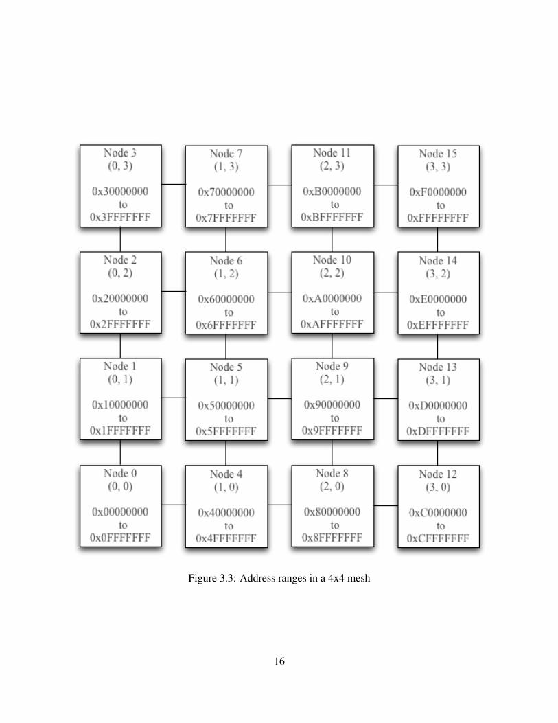
Figure 3.3: Address ranges in a 4x4 mesh
16

the request and ready signal for the local port becomes high simultaneously with the valid signal
on the master AR east port. At this point, node 8 receives a high Valid signal on the slave AR west
port. The same happens in the AR router and assuming another horizontal move the read request
arrives at node 12. After 2 more transfers to the north, the data arrives at the destination node.
This time, when the router decodes the address and finds out that it belongs to this node, instead
of sending it out to any of the four directions it will send the data out on the master AR local port.
This local port, mimics the behavior of the actual master port on the component that initiated this
transaction. Assuming there is a slave component connected to the local interface, the component
receives the read address and sends the data at address 0xED00804C on the R channel through the
local port to the router. Along with the address, node 14 have received the location of the source
of the transaction which is node 4. Therefore, it knows where to send the data. The data on R
channel needs to travel from node 14 to node 4 which requires 2 west moves and 2 south moves.
Immediately after node 14 sends the data from 0xED00804C, it sends the the data on the next
address, 0xED00804D, since the request was for an incrementing burst of length 2. The second
word carries the flag Last which informs the source that this is the last piece of data in the burst. It
also bears a response signal to indicate the status of the transaction from the slave side. The second
word of the burst, also takes two south moves and two west moves, but it does not necessarily take
the same path as the first word. There are defined signals for ordering on the receiver side. When
the last part of the burst data arrives at node 4, the slave R local port on node 4 receives the data
and sends it to the master component.
3.2 Low-Level Design
In this section, a close observation of the inside of the NoC components is provided. Also, their
function, and the structure of their hardware is explained.
17

3.2.1 Inside a Node
Inside each node there are 4 sets of full master/slave NoC interfaces connected to north, east, south,
and west ports and and one local interface connected to the local port. Each set of interfaces has
all 5 channels of AXI on both the master side and the slave side. All signals of the same channel
in a node, are connected to a router assigned to that AXI channel and based on the direction of the
channel, the are placed on the incoming side of the router or the outgoing side. As a result, there
are 5 routers, one for each channel, inside each node. Each router has north, east, south, west, and
local incoming ports, and the same exact ports on the outgoing side. Figure 3.4 shows the inside
of a node.
Based on the direction of each channel on the master side or the slave side of the protocol , they
are assigned to the incoming or the outgoing ports on the router. For instance, in AW router, the
slave channels are on the incoming side and the master channels are on the outgoing side, whereas
in R router, the slave channels are on the outgoing side and the master channels are on the incoming
side. This way, the router decides what direction an incoming data must be sent out.
3.2.2 Data Transfer
For building the channels, simple transmitter and receiver modules have been used. Each of the
incoming channels are connected to a receiver module to handle the handshake between the in-
coming ports of the node and the incoming ports of the router. The transmitters stand between the
outgoing ports of the router and the outgoing ports of the nodes. The receiver modules, also, buffer
the data until the router is ready to serve them.
3.2.2.1 Receiver (RX)
Receiver module packs all the AXI signals of the channel and saves them on a register. When
the router is ready, the data will be transferred and the receiver will become available for the next
incoming data. Figure 3.5 demonstrates the process as a state machine. When the receiver is in idle
state, the ready signal on the corresponding port/channel of the node becomes high. However, the18
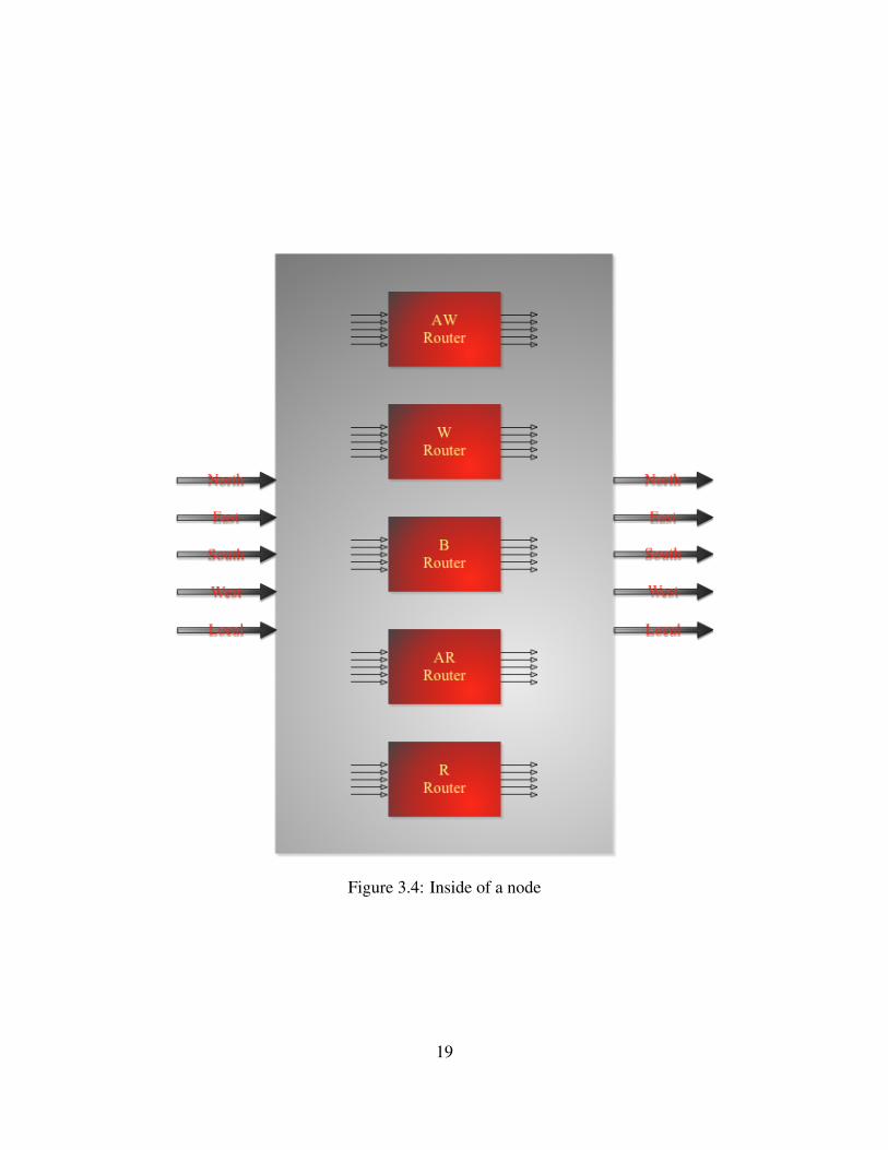
Figure 3.4: Inside of a node
19
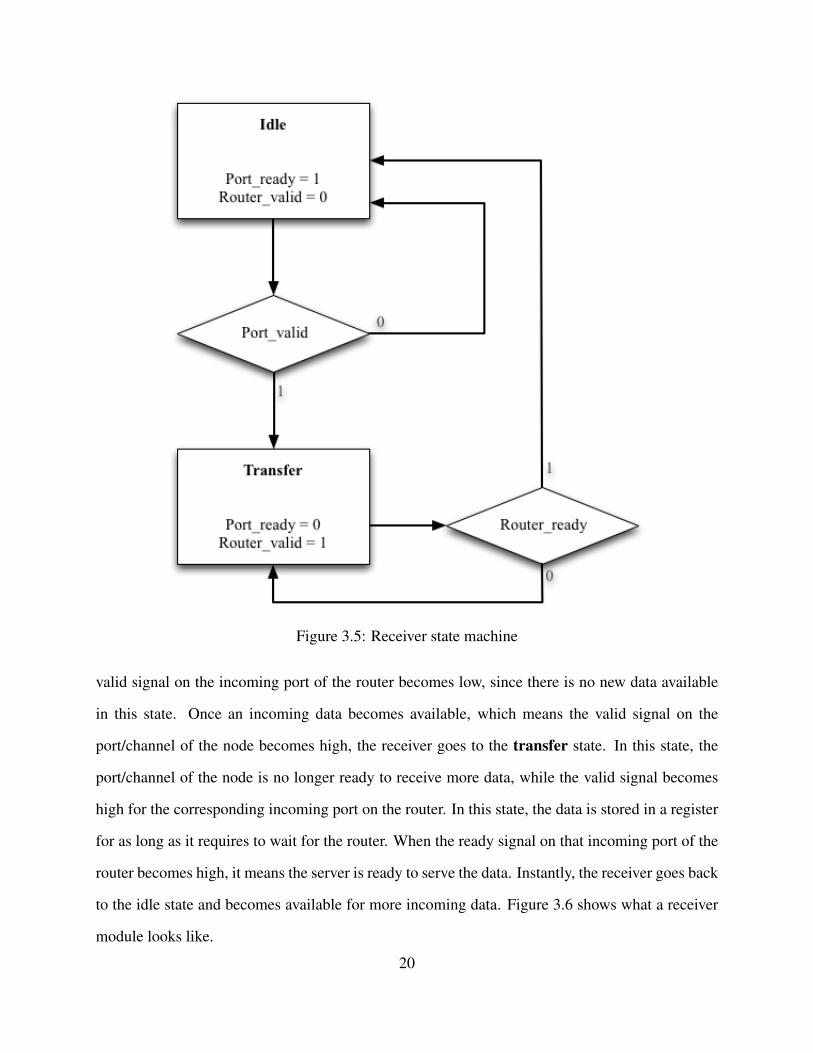
Figure 3.5: Receiver state machine
valid signal on the incoming port of the router becomes low, since there is no new data available
in this state. Once an incoming data becomes available, which means the valid signal on the
port/channel of the node becomes high, the receiver goes to the transfer state. In this state, the
port/channel of the node is no longer ready to receive more data, while the valid signal becomes
high for the corresponding incoming port on the router. In this state, the data is stored in a register
for as long as it requires to wait for the router. When the ready signal on that incoming port of the
router becomes high, it means the server is ready to serve the data. Instantly, the receiver goes back
to the idle state and becomes available for more incoming data. Figure 3.6 shows what a receiver
module looks like.
20
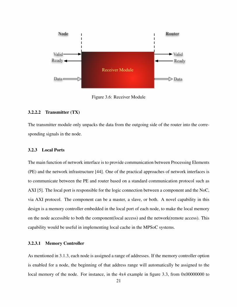
Figure 3.6: Receiver Module
3.2.2.2 Transmitter (TX)
The transmitter module only unpacks the data from the outgoing side of the router into the corre-
sponding signals in the node.
3.2.3 Local Ports
The main function of network interface is to provide communication between Processing Elements
(PE) and the network infrastructure [44]. One of the practical approaches of network interfaces is
to communicate between the PE and router based on a standard communication protocol such as
AXI [5]. The local port is responsible for the logic connection between a component and the NoC,
via AXI protocol. The component can be a master, a slave, or both. A novel capability in this
design is a memory controller embedded in the local port of each node, to make the local memory
on the node accessible to both the component(local access) and the network(remote access). This
capability would be useful in implementing local cache in the MPSoC systems.
3.2.3.1 Memory Controller
As mentioned in 3.1.3, each node is assigned a range of addresses. If the memory controller option
is enabled for a node, the beginning of that address range will automatically be assigned to the
local memory of the node. For instance, in the 4x4 example in figure 3.3, from 0x00000000 to21

0x0FFFFFFF is assigned to node 0. If the local memory is enabled and the size of the memory
is defined as 4KB, then the first 4KB (from 0x00000000 to 0x00000FFF) of the address will be
assigned to the memory and the rest (from 0x00001000 to 0x0FFFFFFF) will be the interface.
The memory controller abstracts the nature of the memory access (local or remote) from the
connected components. On the local port side, if the connected component requests an access and
the address is in the address range of the local memory of its own node, then the memory controller
accesses the memory and handles the AXI handshakes with the interface. However, if the address
does not belong to the node, then the request is for a remote access and it will be passed to the
router to find the path to the destination. Also, on the network side, if an incoming request arrives
at the local port of a node through the router, and the address is in the address range of the local
memory, then the memory controller accesses the memory and then handles the handshakes with
the router. Otherwise the local port sends the request, directly to the interface. Figure 3.7 shows
the connections between the memory, the interface and the network.
3.2.3.2 AXI Master Interface
If a transaction is issued by an AXI master interface such as a processor, then, when it arrives at
the destination, it goes through the master interface of the local port to imitate the behavior of the
source. A master interface is always connected to the slave interface of a component. For instance,
if a slave componentis placed on the NoC, it will be connected to the master interface of the node’s
local port, and therefore, the network is always master for the component.
3.2.3.3 AXI Slave Interface
When a transaction is issued by an AXI slave interface, such as an external memory controller,
then at the destination, the transaction goes through the slave interface to the local port. A slave
interface, similar to master, is always connected to the opposite interface of the connected compo-
nent. A master component on the NoC will always be connected to the slave interface of the local
port, therefore, the network is always slave for a master component. A component can have master
22
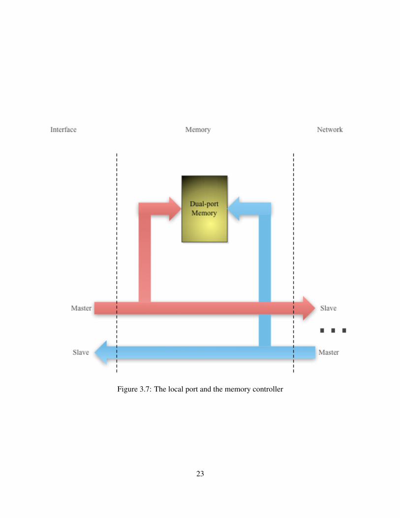
Figure 3.7: The local port and the memory controller
23
side and slave side at the same time and the local interface will handle both sides simultaneously.
3.2.4 Network Ports
Network ports are similar to the local ports. There are master and slave interfaces for all the
directions and each interface has all 5 AXI channels. Each port on a node is connected to an
opposite type port on the adjacent node in the opposite direction. As can be seen in figure 3.2,
each node’s master port is connected to the slave port of the adjacent port in the opposite direction.
For instance, the master W channel of the east port of a node is always connected to the slave
W channel of the west port of the node on its right. The direction of the signals are completely
opposite between master ports and the slave ports, therefore, each master port/channel can be
connected to its equivalent slave port/channel on another node. The direction of the channels are
different in master ports and slave ports. In master ports, AW, W, and AR, are transmitter and B
and R are receiver channels, whereas in slave ports, AW, W, and AR, are receiver ports and B and
R are transmitter ports.
3.2.5 Routers
The design and implementation of a router requires the definition of a set of policies to deal with
packet collision, routing, etc. A NoC router is composed of a number of input ports (connected
to shared NoC ports), a number of output ports (connected to possibly other shared ports), and
a switching matrix connecting the input ports to the output ports. In addition to this physical
connection infrastructure, the router also contains a logic block that implements the flow control
policies (routing, arbitration, etc.) and defines the overall strategy for moving data though the NoC.
A flow control policy characterizes the data movement along the NoC and as such it involves
both global (NoC-level) and local (router-level) issues. One can ensure a deadlock-free routing, for
instance, by taking specific measures in the flow control policy (by avoiding certain paths within
the NoC for example). Also, the optimization of the NoC resources usage (channels, bandwidth,
etc.) and the guarantees on the communication can be ensured as part of the flow control policy
24
(for instance, by choosing a routing algorithm that minimizes the path). Guarantees on the com-
munication performance and quality are known as quality-of-service. Control can be centralized
or distributed. In centralized control, routing decisions are made globally and applied to all nodes,
with an strategy that guarantees no traffic contention. This approach avoids the need for arbitra-
tion units but requires that all nodes share a common sense of time. A possible implementation
of this approach is the use of Time Division Multiplexing (TDM) mechanisms where each packet
is associated to a time frame. However, NoCs typically use a distributed control, where each
router makes decisions locally. Virtual Channels (VCs) implement the concept of multiplexing a
single physical channel over several logically separate channels with individual and independent
buffer queues. The main goal of a VC implementation is to improve performance by avoiding
deadlocks, optimizing wire usage, and providing some traffic guarantees. Deadlock occurs when
network resources are fully occupied and waiting for each other to be released to proceed with the
communication, that is, when two paths are blocked in a cyclic fashion
The routing algorithm is the logic that selects one output port to forward data that has arrived
at the router input. This port is selected according to the routing information available in the packet
header. There are several possible routing algorithms that can be used in a NoC, each one leading to
different trade-offs between performance and cost. For instance, in a deterministic routing, a packet
always uses the same path between two specific nodes. Common deterministic routing schemes
are Source Routing and Dimension Order Routing. In source routing, the source core specifies
the route to the destination. In Dimension Order Routing routing, the packet follows the one
direction first, then moves along the other direction toward the destination. In the adaptive routing,
alternative paths between two nodes may be used if the original path or a local link is congested.
This involves a dynamic evaluation of the link load and implies a dynamic load balancing strategy.
Negative First (NF) and West First (WF) algorithms are examples of adaptive routing algorithms.
In the static routing, paths between cores are defined at compilation time (of the application), while
in the dynamic routing the path is defined at run-time. A unicast routing indicates that a packet
has a single target whereas in the multicast routing a packet can be sent to several nodes in the
25
NoC simultaneously (similar to a bus) or several slaves of a master node. Similarly, a broadcast
communication targets all nodes whereas a narrowcast communication initiated by a master is
related to a single slave associated to it. A routing algorithm can also be classified as minimal or
non-minimal. A minimal routing guarantees that the shortest path to destination is always chosen.
Minimal routing algorithms are those where a bounding box is virtually present and implies that
only decreasing distances from source to destination are valid. On the other hand, non minimal
routing algorithms allow increasing the distance from source to destination. Routing algorithms
can lead to or avoid the occurrence of deadlocks.
While the routing algorithm selects an output port for data, the arbitration logic implemented
in the router selects one input port when multiple packets arrive at the router simultaneously.
Again, one has several options to implement the arbiter: it can be distributed (one per port) or
centralized (one per router), it can be based on static (fixed) or dynamic (variable) priorities among
ports. A centralized arbiter optimizes the use of the router switching matrix, but may lead to
higher latency whereas the distributed approach optimizes the latency. Arbitration logic also de-
fines whether the network assumes a delay or a loss communication model. In the delay model,
packets can be delayed, but never dropped. In the loss model a packet can be dropped as a solution,
for instance, to a congestion situation. In this case, retransmission logic must be implemented as
well.
The switching defines how the data is transmitted from the source node to the target node.
In the circuit switching approach the whole path (including routers and channels) from source
to node is previously established (by the header) and reserved for the transmission of the whole
packet. The payload is not sent until the whole path has been reserved. This can increase latency,
but once the path is defined, this approach can give some guaranteed throughput. In the packet-
based switching approach on the other hand, all flits of the packet are sent as the header establishes
the connection between routers. Still in this model the designer can choose between different
buffering and forward strategies that impact the overall NoC traffic (storing the whole packet in
each router before establishing the connection to the next router or sending the flits in a pipeline
26
mode for instance). In the store-and-forward strategy, the node stores the complete packet before
forwarding it to the next node in the path. In this strategy one must ensure that the buffer size at
each node is sufficient to store the whole packet or the packet can be stalled. In the wormhole
strategy, on the other hand, the node makes the routing decision and forwards the packet as soon as
the header arrives. The subsequent flits follow the header as they arrive. This reduces the latency
within the router, but in case of packet stalling, many links risk to be locked at once. The virtual-
cut-through mechanism is similar to the wormhole approach but, before forwarding the first data
flit to the next node in the path, the node waits for a confirmation that the whole packet can be
accepted by the next node. Thus, in case of stalling, no links are affected, only the current node.
The buffering policy is the strategy used to store information in the router when there is con-
gestion in the network and a packet cannot be forwarded right away. The buffering strategy (num-
ber, location and size of the buffers), has an important impact on the network traffic and, therefore,
on the NoC performance. In addition, the buffers are responsible for a large portion of the router
area. One can have a single buffer in the router, shared by all input ports, or one can have one buffer
per port (input or output). The main advantage of the first approach is the area optimization, but
the control can be more complex and additional care must be taken to deal with buffer overflow. In
the distributed approach, each input port has its own buffer and the most common implementation
is in the form of a FIFO, although other implementations are also possible. Distributed output
buffers are also possible, but they tend to be less efficient because several input ports may need to
store data in a single structure.
In this design, VC type distributed flow control is used and the routers make the decision
locally. The routing algorithm is adaptive and it depends on the traffic of the channels. The
arbitration logic is distributed so each channel has its own arbitration, and the arbitration priorities
are fixed. This design uses packet switching and considering a burst transaction, a packet, then the
packet switching uses the wormhole strategy for storing and forwarding. Each part of the burst
data is served individually and all the pieces do not necessarily take the same path. The buffering
policy, as mentioned in 3.2.2.1 is storing the data at the receiver side of each transfer, until further
27
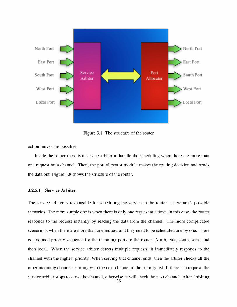
Figure 3.8: The structure of the router
action moves are possible.
Inside the router there is a service arbiter to handle the scheduling when there are more than
one request on a channel. Then, the port allocator module makes the routing decision and sends
the data out. Figure 3.8 shows the structure of the router.
3.2.5.1 Service Arbiter
The service arbiter is responsible for scheduling the service in the router. There are 2 possible
scenarios. The more simple one is when there is only one request at a time. In this case, the router
responds to the request instantly by reading the data from the channel. The more complicated
scenario is when there are more than one request and they need to be scheduled one by one. There
is a defined priority sequence for the incoming ports to the router. North, east, south, west, and
then local. When the service arbiter detects multiple requests, it immediately responds to the
channel with the highest priority. When serving that channel ends, then the arbiter checks all the
other incoming channels starting with the next channel in the priority list. If there is a request, the
service arbiter stops to serve the channel, otherwise, it will check the next channel. After finishing28
the routing service for one incoming channel, the arbiter always checks the next channel, even
if there are other requests waiting in the queue of the same channel. This method, prevents the
channels from starvation. For instance, if the incoming ports north, west, and local, request service
on the AW channel router, the north channel will be served immediately. When it’s finished, the
arbiter checks the east channel and then south channel (each channel test happens in one clock
cycle) and it skips them because there are no requests. When the arbiter reaches the west channel
it stops and serves the west channel. When this one is over, then there will be only one request on
the local port and the arbiter, schedules a single request by jumping directly to that request.
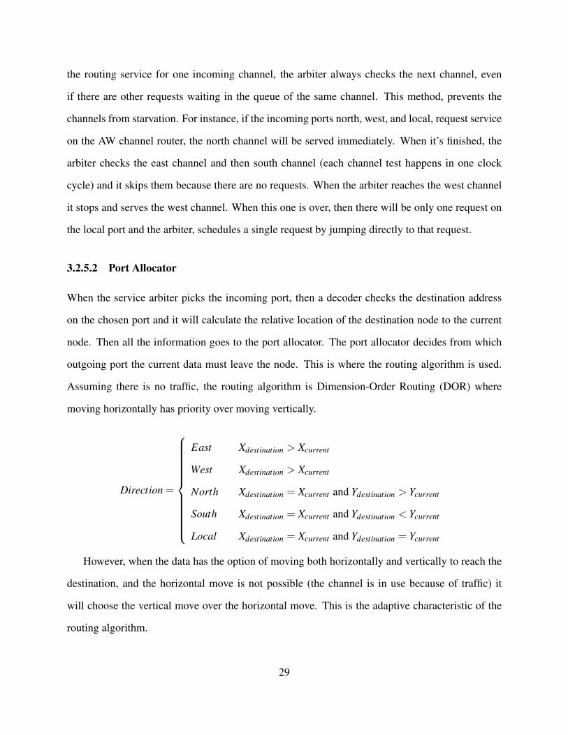
3.2.5.2 Port Allocator
When the service arbiter picks the incoming port, then a decoder checks the destination address
on the chosen port and it will calculate the relative location of the destination node to the current
node. Then all the information goes to the port allocator. The port allocator decides from which
outgoing port the current data must leave the node. This is where the routing algorithm is used.
Assuming there is no traffic, the routing algorithm is Dimension-Order Routing (DOR) where
moving horizontally has priority over moving vertically.
Direction =
East Xdestination > Xcurrent
West Xdestination > Xcurrent
North Xdestination = Xcurrent and Ydestination > Ycurrent
South Xdestination = Xcurrent and Ydestination < Ycurrent
Local Xdestination = Xcurrent and Ydestination = Ycurrent
However, when the data has the option of moving both horizontally and vertically to reach the
destination, and the horizontal move is not possible (the channel is in use because of traffic) it
will choose the vertical move over the horizontal move. This is the adaptive characteristic of the
routing algorithm.
29
3.2.6 Top Level
After designing all the pieces, a top-level design is required to create the mesh network. The top
level design instantiates the nodes, customizes them, and makes the proper connections between
them. For instance, if the goal is building a 4x4 mesh, the top level design instantiates 16 nodes as
a 2 dimensional matrix. Then, based on the user configurations, it customizes the nodes by adding
local memory of the defined size to the defined nodes, and adding master local interface, slave
local interface, or both, to each node based on the defined characteristics of the node. Finally, for
the mesh to function properly, the proper connection between the adjacent nodes must be made. A
master port is always connected to a slave port of the same channel in its adjacent node. When the
mesh is created, the top level design, maps the local ports to the input/output ports.
Creating each top level design, even by taking advantage of the multi-dimensional arrays of
signals and loops, is a time-consuming process. In order to ease the process of creating NoCs with
a particular design scenario, there is a script that gathers information from the user about the size
of the mesh, the size of each dimension, and the customizations on each node, and generates the
top level design.
3.3 Implementation
This NoC was designed in a top-down approach starting with the mesh. The mesh was broken
down to nodes, and then in each node the routers, channel interfaces and local-port interface were
designed. The channels were divided into the master side and the slave side and each side was
divided into 5 different AXI channels. Then each channel was designed using transmitter and
receiver modules. The tasks in the routers were distributed between the service arbiter, the port
allocator and a decoder for the destination address. The local ports were designed using dual-port
memory blocks and the controller logic for the memory controller and the interface. After the
design phase, the modeling of the design was done using VHDL. The components were modeled
from the bottom up. Each small component was modeled, tested and verified. Then the small com-
30

ponents were integrated to build larger components and did the same testing and verification parts.
At the end, to test and verify the functionality of the NoC, more elaborate tests were designed. The
design was implemented on Xilinx Virtex-7 FPGAs using VC707 boards and the version 14.3 of
the tools.
31
Chapter 4
Results
4.1 Verification
For this design, directed verification technique was used. The verification was done both at the
component level, after each component was designed and modeled, and at the system level when
the entire system was designed, and modeled. Although Constrained Random Testing (CRT) ver-
ification technique was not used, the directed verification plan was designed carefully to cover as
much of the corner cases as possible. The tests were designed as VHDL test-benches and the math-
ematical functions inside were used to generate different cases based on the scenario of the test.
The waveforms were observed in ModelSim. In order to automate the testing process, the Mod-
elSim Tcl scripts were created and also Make files were used to run them in the right sequence.
At the debugging process, both at the component level and the system level, the tests were run
several times, and without the automated testing, the testing and verification process would have
been excessively time-consuming.
4.1.1 Component Verification
After finishing each component, a test-bench was designed specifically to verify the function of
that component. Some of the components were small enough so it was possible to test every
possible case. For instance, in the receiver, combining all the possible cases for the handshakes on
both sides or in the port arbiter, and testing the entire range of the 32 bit address on the design was
feasible. For larger designs, such as a full master/slave AXI channel, covering all the possibilities
was not feasible. For cases like this, as much of the corner cases as possible were tested on each
channel for several scenarios. For the AXI channel, different situations on each single channel were
tried simultaneously with the other channels. Verifying each component means the component
functions exactly as desired. After integrating the small components, the functionality becomes32
more complex and designing the verification plan becomes more difficult and time-consuming.
4.1.2 System Verification
System verification was done after a complete NoC with the already verified components was
created. At this stage the functionality of the system as a whole, was tested. The tests started with
simpler scenarios and after each phase, the complexity of the scenarios were increased. In each
phase, bugs were found and fixed until the system was functioning correctly. A 4x4 mesh was
the subject of the system-level verification to have a reasonable balance between having a system
small enough to be observed clock-cycle by clock-cycle and large enough to implement all the
possible complexities in a test scenario.
4.1.2.1 Phase One
In this phase, two nodes in the network are picked. Then, from the local interface of the first node, a
write transaction is initiated to be sent to the second node. At the second node, if the signals arrive
correctly, a process emulates a slave component and stores the write data in the requested address
and the correct response signals are sent back to the source. This process is done for burst lengths
from 1 to 255 and for addresses both in the local memory range and the interface range. A table
in the source node stores all the sent addresses and the data associated with them. Then the same
source node reads the written data from the same destination in a different order and compares
the read data to the table and checks if the correct data has been read from the destination. The
same test is repeated for several pairs of nodes. The completion of this phase verified that single
transactions in a NoC, with no traffic caused by other nodes, work correctly.
4.1.2.2 Phase Two
Phase two added the effect of traffic to phase one. In this phase, a node is picked as the source of
the transactions. Then, from the selected node, write transactions were sent to all the other nodes
in the system. A table in the source node is assigned to each node in the system. This table stores33
the addresses that are used in the write transactions and the data associated to those addresses. To
make the verification easier, a particular range of data is assigned to each node so when they are
read back, they are identifiable. The transactions cover all the possible burst lengths. Then, the
source node reads data from every node in the system and compares the read data to the content
of the table. The test was repeated for several nodes as the source. The completion of this phase
verified that in a network with a light traffic, transactions reach their destination with no fault.
4.1.2.3 Phase Three
Phase three is a more complex version of phase 2 with heavy traffic. In this phase, every single
node in the NoC is a source node such as the one described in phase two. Each node sends write
transactions to all the other nodes in the network, and they all work simultaneously. Then each
source reads back from all the other nodes and compares it to it’s table. This process creates a
heavy traffic in the system. This test, evaluates the master side, of the interface, the slave side, and
also the memory controller. The completion of this phase verified that in a network with heavy
traffic, transactions reach their destination with no fault.
4.2 Resource Utilization
To analyze the resource utilization of the NoC, different sized of mesh with different configurations
were synthesized for Xilinx Virtex-7 FPGA. Table 4.1 shows the synthesis results for 2x2, 3x3,
4x4, 5x5, 6x6, and 7x7 meshes and it shows the resource utilization for flop-flops, LUTs and
Block RAMs. Also, figure 4.1 visualizes the results. The growth of the resource utilization is
almost linear with the growth of the number of the nodes. Also, the systems with local memory
controller enabled use slightly more resources than the ones without the controller. As an analogy,
the resource utilization between a 4x4 NoC and a bus-based MPSoC system[10] of the same scale,
synthesized for the same platform were compared. Both the NoC and the bus-based system utilize
3% of the flip-flops. The NoC uses 11% of the LUTs while the bus-based system uses only 8.5%.
The comparison for block RAMs are irrelevant because the size of the memories can vary.34
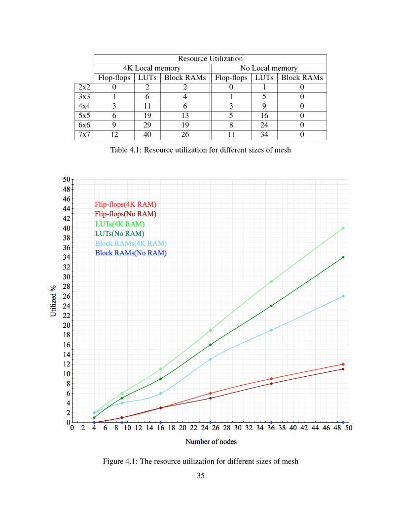
Resource Utilization4K Local memory No Local memory
Flop-flops LUTs Block RAMs Flop-flops LUTs Block RAMs2x2 0 2 2 0 1 03x3 1 6 4 1 5 04x4 3 11 6 3 9 05x5 6 19 13 5 16 06x6 9 29 19 8 24 07x7 12 40 26 11 34 0
Table 4.1: Resource utilization for different sizes of mesh
Figure 4.1: The resource utilization for different sizes of mesh
35
4.3 Time Analysis
In this section, the performance of the NoC is analyzed by observing the time it takes for a trans-
action to finish which is directly related to the length of the path between the source and the des-
tination. Also, the time it takes for data to traverse from a node to the adjacent node is calculated.
For this experiment, a 7x7 mesh was created. A node was selected as source and several other
nodes as destination. The source node is node 0 (the bottom left corner of the mesh). To make
the result of the experiment deterministic, the data was transfered without any interfering traffic.
When there is no interfering traffic in the way, the routers always respond instantly without making
the transaction wait in line until another transaction is served. Each transaction is a remote read of
size 1 (no burst). At the source node, a process in the test-bench initiates read transactions to go
to different nodes. In all the other nodes a process is always waiting for read requests and when it
receives one, it responds instantly. This way, only the latency of the network is measured without
the effect of the latency of the components connected to the NoC. The source process produces 12
different transactions for 12 different destinations in the mesh. The destination of each transaction
is different than the other one. The distance from the source to the destination varies from 1 hop
to 12 hops (longest path in a 7x7 mesh). Table 4.2 shows the results. Each transaction consists of
a AR request from the source to destination and a R data coming back from the destination node
to node 0. The results show that in all cases, passing through each node (including source node)
takes 5 clock cycles and it takes one clock cycle for each local interface to transfer data between
the component and the NoC. The following equation was extracted from table 4.2 and it shows the
latency of the path.
Of course this observation is an ideal case and when there is traffic in the network, the delays
increase. In MPSoCs, nodes with higher volume of communication must be placed as close as
possible to achieve the minimum delay in the system. For instance, if the main processor and a
memory subsystem in a MPSoC, communicate frequently, the optimal delay is achieved by placing
them in adjacent nodes in the mesh.
36
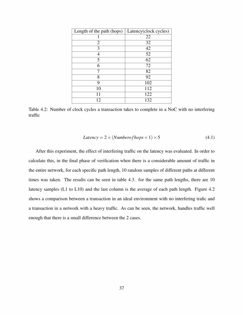
Length of the path (hops) Latency(clock cycles)1 222 323 424 525 626 727 828 929 102
10 11211 12212 132
Table 4.2: Number of clock cycles a transaction takes to complete in a NoC with no interferingtraffic
Latency = 2× (Numbero f hops+1)×5 (4.1)
After this experiment, the effect of interfering traffic on the latency was evaluated. In order to
calculate this, in the final phase of verification when there is a considerable amount of traffic in
the entire network, for each specific path length, 10 random samples of different paths at different
times was taken. The results can be seen in table 4.3. for the same path lengths, there are 10
latency samples (L1 to L10) and the last column is the average of each path length. Figure 4.2
shows a comparison between a transaction in an ideal environment with no interfering trafic and
a transaction in a network with a heavy traffic. As can be seen, the network, handles traffic well
enough that there is a small difference between the 2 cases.
37
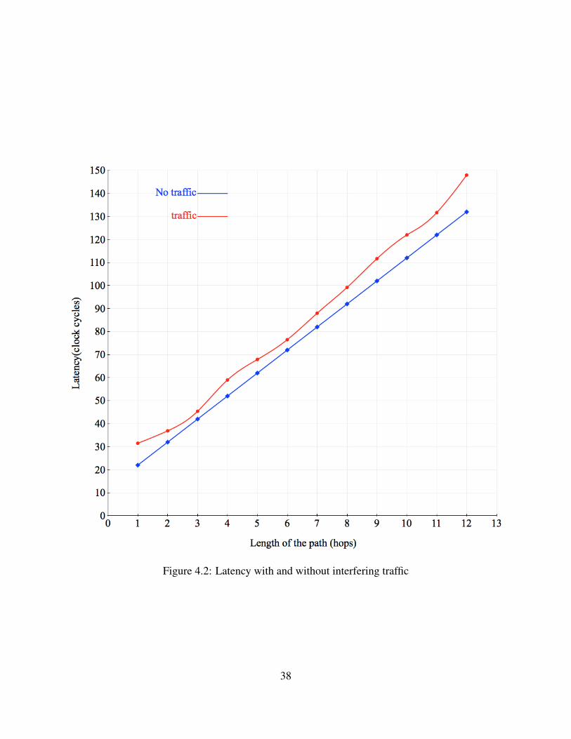
Figure 4.2: Latency with and without interfering traffic
38
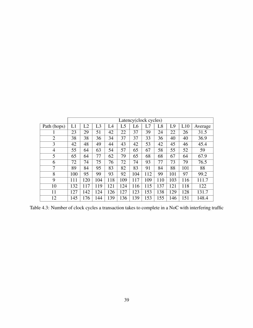
Latency(clock cycles)Path (hops) L1 L2 L3 L4 L5 L6 L7 L8 L9 L10 Average
1 23 29 51 42 22 37 39 24 22 26 31.52 38 38 36 34 37 37 33 36 40 40 36.93 42 48 49 44 43 42 53 42 45 46 45.44 55 64 63 54 57 65 67 58 55 52 595 65 64 77 62 79 65 68 68 67 64 67.96 72 74 75 76 72 74 93 77 73 79 76.57 89 84 95 83 82 83 91 84 88 101 888 100 95 99 93 92 104 112 99 101 97 99.29 111 120 104 118 109 117 109 110 103 116 111.7
10 132 117 119 121 124 116 115 137 121 118 12211 127 142 124 126 127 123 153 138 129 128 131.712 145 176 144 139 136 139 153 155 146 151 148.4
Table 4.3: Number of clock cycles a transaction takes to complete in a NoC with interfering traffic
39
Chapter 5
Conclusion
With the growth of of the number of components in SoCs, and more specifically the number of
processors in MPSoCs, having reliable, robust and scalable interconnect has become a major part
of every design. The most important issue in designing interconnect, is choosing an interconnect
based on the requirements of the system. The volume of the traffic, the characteristics of the
transactions, and the hardware infrastructure, together define what kind of interconnect is suitable
for the system. In multi-processor systems, the interconnect must provide specific services to the
clients (which are mostly processors) as efficiently as possible.
This project was designed based on the characteristics of a multi-processor system imple-
mented on Xilinx FPGAs. The system is called Hthreads [10] and it uses thread-based program-
ming to take advantage of the multiprocessing characteristics of the system by scheduling threads
to be executed on PEs in parallel. The type of the communications are normally read/writes of
small chunks of data between the nodes, and occasionally the DMA type communication of bigger
chunks between the host processor and the slave processors when a thread is assigned to a PE.
This NoC was initially designed only for AXI-Lite type (no burst) communication. Then to take
advantage of the burst capabilities of AXI protocol for DMA, the system was upgraded to support
burst. The NoC can handle more traffic than the current Hthread system can produce, but the fu-
ture generations of Hthreads with higher volume of interaction between the PEs will require such
a capable interconnect.
The main characteristics of this interconnect that make it suitable specifically for MPSoC sys-
tems are as follows:
• An important characteristic that the majority of multi-processor systems have in common is
having local memory for each PE. The local memory can be interpreted as a private cache
or just a local memory space for the processor. This design provides an embedded support40
for local memory. The memory is mapped to the node’s address space and a smart memory
controller compiles the transactions into series of memory accesses and also provides the
feedback signals for the PE
• several aspects of the transactions were abstracted to make it easier for the clients to com-
municate with the NoC. The first aspect was the remoteness or the locality of the transaction.
From the network client’s perspective, there is no difference between a remote access and a
local access because the transactions look the same. What differentiates a local access from
a remote access is , to which address domain the transaction address belongs. The other
aspect was whether the receiver of the transaction was another network client or a memory.
The memory controller makes the response from a memory access look exactly the same as
the response from an access to another client.
• This NoC is customizable in several areas. The network interface can be customized to in-
clude master interface, slave interface, or both, on each individual node. Also, each node can
have the local memory available or disable the memory controller based on the requirements
of the node. In addition, the size of the local memory is customizable for each single node.
5.1 Research Contributions
The purpose of this research was to provide a scalable and reliable mesh Network-on-Chip for
MPSoCs, as well as the support for embedded local memory on the nodes. This platform allows
the components on a MPSoCs to communicate with each other by assigning an address range to
each component and abstracting the difference between the way local accesses and remote accesses
are processed in the network interface. Some of the contributions of this project include:
• Designing a mesh Network-on-Chip with AMBA AXI interface.
• Supporting embedded local memory for nodes, interfacing it both to the interface and to the
rest of the network, and automatically assigning the memory to the beginning part of the
node’s address range41

• Adding customizability to each node’s interface so they can have master side, slave side, or
both, and also enabling or disabling the local memory controller.
• Designing thorough directed testbenches to verify the system and cover as much cases as
possible
5.2 Future Work
Designing the script to create the top-level design has made experimenting with different sizes
of mesh with different configurations very easy. As a part of the future work, The script can be
connected to a front-end web interface to be accessed online easily, without running the script and
passing the system configurations to it. Moreover, the same architecture can be used for other
topologies. The nodes are designed with 4 network links to be placed in a mesh network. With
slight adjustment in the routers and the nodes, the same architecture can be used to create a ring or
a tree. Finally, the router can be optimized to spend less sequences on the decision making process.
There needs to be different tests to find an optimum spot in the trade-off between the number of
sequences and the resource utilization in the router.
42
References
[1] P. Abad, P. Prieto, L.G. Menezo, A. Colaso, V. Puente, and J.-A. Gregorio. Topaz: An open-source interconnection network simulator for chip multiprocessors and supercomputers. InNetworks on Chip (NoCS), 2012 Sixth IEEE/ACM International Symposium on, pages 99–106, 2012.
[2] V. Agarwal, M. S. Hrishikesh, S.W. Keckler, and D. Burger. Clock rate versus ipc: the end ofthe road for conventional microarchitectures. In Computer Architecture, 2000. Proceedingsof the 27th International Symposium on, pages 248–259, 2000.
[3] N. Alfaraj, Junjie Zhang, Yang Xu, and H.J. Chao. Hope: Hotspot congestion control forclos network on chip. In Networks on Chip (NoCS), 2011 Fifth IEEE/ACM InternationalSymposium on, pages 17–24, 2011.
[4] A. Allan, D. Edenfeld, W.H. Joyner, A.B. Kahng, M. Rodgers, and Y. Zorian. 2001 technol-ogy roadmap for semiconductors. Computer, 35(1):42–53, 2002.
[5] ARM. AMBA AXI and ACE Protocol Specification. http://infocenter.arm.com/help/index.jsp?topic=/com.arm.doc.set.amba/index.html. Last accessed February 14, 2014.
[6] Y. Ben-Itzhak, I. Cidon, and A. Kolodny. Delay analysis of wormhole based heterogeneousnoc. In Networks on Chip (NoCS), 2011 Fifth IEEE/ACM International Symposium on, pages161–168, 2011.
[7] L. Benini and G. De Micheli. Networks on chips: a new soc paradigm. Computer, 35(1):70–78, 2002.
[8] L. Benini and G. De Micheli. Networks on chips: a new soc paradigm. Computer, 35(1):70–78, 2002.
[9] L.P. Carloni, P. Pande, and Yuan Xie. Networks-on-chip in emerging interconnect paradigms:Advantages and challenges. In Networks-on-Chip, 2009. NoCS 2009. 3rd ACM/IEEE Inter-national Symposium on, pages 93–102, 2009.
[10] E. Cartwright, A. Fahkari, S. Ma, C. Smith, M. Huang, D. Andrews, and J. Agron. Au-tomating the design of mlut mpsopc fpgas in the cloud. In Field Programmable Logic andApplications (FPL), 2012 22nd International Conference on, pages 231–236, 2012.
[11] Steve Leibson Chris Rowen. Engineering the Complex SOC: Fast, Flexible Design withConfigurable Processors. Prentice Hall PTR, 2004.
[12] Theo A C M Claasen. An industry perspective on current and future state of the art in system-on-chip (soc) technology. Proceedings of the IEEE, 94(6):1121–1137, 2006.
[13] W.J. Dally and B. Towles. Route packets, not wires: on-chip interconnection networks. InDesign Automation Conference, 2001. Proceedings, pages 684–689, 2001.
43

[14] M. Daneshtalab, M. Ebrahimi, P. Liljeberg, J. Plosila, and H. Tenhunen. A low-latency andmemory-efficient on-chip network. In Networks-on-Chip (NOCS), 2010 Fourth ACM/IEEEInternational Symposium on, pages 99–106, 2010.
[15] M.A.A. El Ghany, M.A. El-Moursy, and M. Ismail. High throughput architecture for cliche;network on chip. In SOC Conference, 2009. SOCC 2009. IEEE International, pages 155–158,2009.
[16] R. Ho, K.W. Mai, and M.A. Horowitz. The future of wires. Proceedings of the IEEE,89(4):490–504, 2001.
[17] R. Holsmark, S. Kumar, M. Palesi, and A. Mejia. Hira: A methodology for deadlockfree routing in hierarchical networks on chip. In Networks-on-Chip, 2009. NoCS 2009. 3rdACM/IEEE International Symposium on, pages 2–11, 2009.
[18] M. Horowitz and W. Dally. How scaling will change processor architecture. In Solid-StateCircuits Conference, 2004. Digest of Technical Papers. ISSCC. 2004 IEEE International,pages 132–133 Vol.1, 2004.
[19] Y. Hoskote, S. Vangal, A. Singh, N. Borkar, and S. Borkar. A 5-ghz mesh interconnect for ateraflops processor. Micro, IEEE, 27(5):51–61, 2007.
[20] Cheng-Ta Hsieh and M. Pedram. Architectural energy optimization by bus split-ting. Computer-Aided Design of Integrated Circuits and Systems, IEEE Transactions on,21(4):408–414, 2002.
[21] A. Iyer and D. Marculescu. Power and performance evaluation of globally asynchronouslocally synchronous processors. In Computer Architecture, 2002. Proceedings. 29th AnnualInternational Symposium on, pages 158–168, 2002.
[22] Axel Jantsch and Hannu Tenhunen, editors. Networks on Chip. Kluwer Academic Publishers,Hingham, MA, USA, 2003.
[23] S. Jovanovic, C. Tanougast, S. Weber, and C. Bobda. A new deadlock-free fault-tolerantrouting algorithm for noc interconnections. In Field Programmable Logic and Applications,2009. FPL 2009. International Conference on, pages 326–331, 2009.
[24] H. Kariniemi and J. Nurmi. On-line reconfigurable xgft network-on-chip designed for im-proving the fault-tolerance and manufacturability of the mpsoc chips. In Field ProgrammableLogic and Applications, 2006. FPL ’06. International Conference on, pages 1–6, 2006.
[25] Kangmin Lee, Se-Joong Lee, and Hoi-Jun Yoo. Low-power network-on-chip for high-performance soc design. Very Large Scale Integration (VLSI) Systems, IEEE Transactionson, 14(2):148–160, 2006.
[26] M. Lodde, J. Flich, and M.E. Acacio. Heterogeneous noc design for efficient broadcast-based coherence protocol support. In Networks on Chip (NoCS), 2012 Sixth IEEE/ACMInternational Symposium on, pages 59–66, 2012.
44
[27] Zhonghai Lu. Design and analysis of on-chip communication for network-on-chip platforms.Master’s thesis, KTH, 2007.
[28] P. Mahr and C. Bobda. Reducing communication costs on dynamic networks-on-chip throughruntime relocation of tasks. In Rapid System Prototyping (RSP), 2012 23rd IEEE Interna-tional Symposium on, pages 177–182, 2012.
[29] J.W. McPherson. Reliability challenges for 45nm and beyond. In Design Automation Con-ference, 2006 43rd ACM/IEEE, pages 176–181, 2006.
[30] N. Michael, M. Nikolov, Ao Tang, G.E. Suh, and C. Batten. Analysis of application-awareon-chip routing under traffic uncertainty. In Networks on Chip (NoCS), 2011 Fifth IEEE/ACMInternational Symposium on, pages 9–16, 2011.
[31] M. Millberg, E. Nilsson, R. Thid, S. Kumar, and A. Jantsch. The nostrum backbone-a com-munication protocol stack for networks on chip. In VLSI Design, 2004. Proceedings. 17thInternational Conference on, pages 693–696, 2004.
[32] T. Mudge. Power: a first-class architectural design constraint. Computer, 34(4):52–58, 2001.
[33] B. Osterloh, H. Michalik, B. Fiethe, and K. Kotarowski. Socwire: A network-on-chip ap-proach for reconfigurable system-on-chip designs in space applications. In Adaptive Hard-ware and Systems, 2008. AHS ’08. NASA/ESA Conference on, pages 51–56, 2008.
[34] P.P. Pande, C. Grecu, M. Jones, A. Ivanov, and R. Saleh. Performance evaluation and designtrade-offs for network-on-chip interconnect architectures. Computers, IEEE Transactions on,54(8):1025–1040, 2005.
[35] Michael K. Papamichael and James C. Hoe. Connect: Re-examining conventional wisdomfor designing nocs in the context of fpgas. In Proceedings of the ACM/SIGDA InternationalSymposium on Field Programmable Gate Arrays, FPGA ’12, pages 37–46, New York, NY,USA, 2012. ACM.
[36] Leena Singh Prakash Rashinkar, Peter Paterson. System-on-a-Chip Verification. Springer,2001.
[37] Yue Qian, Zhonghai Lu, and Wenhua Dou. Analysis of worst-case delay bounds for best-effort communication in wormhole networks on chip. In Networks-on-Chip, 2009. NoCS2009. 3rd ACM/IEEE International Symposium on, pages 44–53, 2009.
[38] V. Raghunathan, M.B. Srivastava, and R.K. Gupta. A survey of techniques for energy efficienton-chip communication. In Design Automation Conference, 2003. Proceedings, pages 900–905, 2003.
[39] E. Salminen, A. Kulmala, and T.D. Hamalainen. On network-on-chip comparison. In DigitalSystem Design Architectures, Methods and Tools, 2007. DSD 2007. 10th Euromicro Confer-ence on, pages 503–510, Aug 2007.
45
[40] Keun Sup Shim, Myong Hyon Cho, M. Kinsy, T. Wen, M. Lis, G.E. Suh, and S Devadas.Static virtual channel allocation in oblivious routing. In Networks-on-Chip, 2009. NoCS2009. 3rd ACM/IEEE International Symposium on, pages 38–43, 2009.
[41] A.T. Tran, D.N. Truong, and B.M. Baas. A gals many-core heterogeneous dsp platform withsource-synchronous on-chip interconnection network. In Networks-on-Chip, 2009. NoCS2009. 3rd ACM/IEEE International Symposium on, pages 214–223, 2009.
[42] Danyao Wang, N.E. Jerger, and J.G. Steffan. Dart: A programmable architecture for nocsimulation on fpgas. In Networks on Chip (NoCS), 2011 Fifth IEEE/ACM International Sym-posium on, pages 145–152, 2011.
[43] Jian Wang, Yubai Li, Qicong Peng, and Taiqiu Tan. A dynamic priority arbiter for network-on-chip. In Industrial Embedded Systems, 2009. SIES ’09. IEEE International Symposiumon, pages 253–256, 2009.
[44] C.A. Zeferino, M.E. Kreutz, and A.A. Susin. Rasoc: a router soft-core for networks-on-chip.In Design, Automation and Test in Europe Conference and Exhibition, 2004. Proceedings,volume 3, pages 198–203 Vol.3, 2004.
[45] Li-Rong Zheng. Design, analysis and integration of mixed-signal systems for signal andpower integrity. PhD thesis, KTH, 2001.
46