Embed Size (px)
Citation preview
i
Designing and Building the Vermonster Mini
Dual-Resonant Solid State Tesla Coil
Table Of Contents
The Design………………………………………………………………………………………….1
Tesla Coil Basics..........................................................................1
Secondary Coil Design................................................................3
Primary Circuit Design................................................................6
Schematic Design........................................................................12
Interrupter......................................................................12
Soft-Switching Circuitry...................................................13
Driver Chips.....................................................................15
Gate Drive Transformers..................................................16
H-Bridge...........................................................................17
Tesla Coil..........................................................................18
Feedback..........................................................................19
Over-Current Detection....................................................20
Interrupter Design…………………………………………………………………….21
Driver Design…………………………………………………………………………….22
H-Bridge Design…………………………………………………………………………26
Feedback Design………………………………………………………………………..28
The Build……………………………………………………………………………………………….29
Building the Secondary Coil……………………………………………………….29
Building the Topload………………………………………………………………….31
ii
Building the Capacitor Bank………………………………………………………31
Building the Primary Coil…………………………………………………………..32
Building the Strike Rail………………………………………………………………35
Building the Gate Drive Transformers……………………………………….38
Building the Bridge……………………………………………………………………39
Building the Driver…………………………………………………………………….43
Building the Current Sense Transformers………………………………….43
Building the Protection Circuitry……………………………………………….44
Testing………………………………………………………………………………………………….48
Low Power Testing…………………………………………………………………….48
High Power Testing…………………………………………………………………….50
First Light……………………………………………………………………………………54
Tuning………………………………………………………………………………………..56
Future Plans…………………………………………………………………………………………...59
1
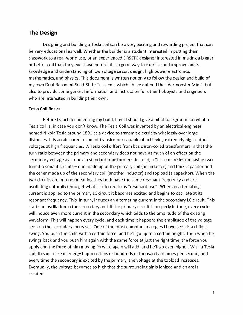
The Design
Designing and building a Tesla coil can be a very exciting and rewarding project that can
be very educational as well. Whether the builder is a student interested in putting their
classwork to a real-world use, or an experienced DRSSTC designer interested in making a bigger
or better coil than they ever have before, it is a good way to exercise and improve one’s
knowledge and understanding of low voltage circuit design, high power electronics,
mathematics, and physics. This document is written not only to follow the design and build of
my own Dual-Resonant Solid-State Tesla coil, which I have dubbed the “Vermonster Mini”, but
also to provide some general information and instruction for other hobbyists and engineers
who are interested in building their own.
Tesla Coil Basics
Before I start documenting my build, I feel I should give a bit of background on what a
Tesla coil is, in case you don’t know. The Tesla Coil was invented by an electrical engineer
named Nikola Tesla around 1891 as a device to transmit electricity wirelessly over large
distances. It is an air-cored resonant transformer capable of achieving extremely high output
voltages at high frequencies. A Tesla coil differs from basic iron-cored transformers in that the
turn ratio between the primary and secondary does not have as much of an effect on the
secondary voltage as it does in standard transformers. Instead, a Tesla coil relies on having two
tuned resonant circuits – one made up of the primary coil (an inductor) and tank capacitor and
the other made up of the secondary coil (another inductor) and topload (a capacitor). When the
two circuits are in tune (meaning they both have the same resonant frequency and are
oscillating naturally), you get what is referred to as “resonant rise”. When an alternating
current is applied to the primary LC circuit it becomes excited and begins to oscillate at its
resonant frequency. This, in turn, induces an alternating current in the secondary LC circuit. This
starts an oscillation in the secondary and, if the primary circuit is properly in tune, every cycle
will induce even more current in the secondary which adds to the amplitude of the existing
waveform. This will happen every cycle, and each time it happens the amplitude of the voltage
seen on the secondary increases. One of the most common analogies I have seen is a child’s
swing: You push the child with a certain force, and he’ll go up to a certain height. Then when he
swings back and you push him again with the same force at just the right time, the force you
apply and the force of him moving forward again will add, and he’ll go even higher. With a Tesla
coil, this increase in energy happens tens or hundreds of thousands of times per second, and
every time the secondary is excited by the primary, the voltage at the topload increases.
Eventually, the voltage becomes so high that the surrounding air is ionized and an arc is
created.
2
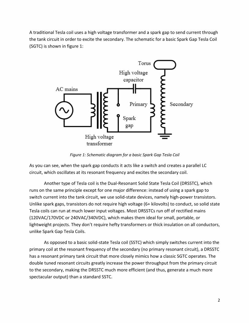
A traditional Tesla coil uses a high voltage transformer and a spark gap to send current through
the tank circuit in order to excite the secondary. The schematic for a basic Spark Gap Tesla Coil
(SGTC) is shown in figure 1:
Figure 1: Schematic diagram for a basic Spark Gap Tesla Coil
As you can see, when the spark gap conducts it acts like a switch and creates a parallel LC
circuit, which oscillates at its resonant frequency and excites the secondary coil.
Another type of Tesla coil is the Dual-Resonant Solid State Tesla Coil (DRSSTC), which
runs on the same principle except for one major difference: instead of using a spark gap to
switch current into the tank circuit, we use solid-state devices, namely high-power transistors.
Unlike spark gaps, transistors do not require high voltage (6+ kilovolts) to conduct, so solid state
Tesla coils can run at much lower input voltages. Most DRSSTCs run off of rectified mains
(120VAC/170VDC or 240VAC/340VDC), which makes them ideal for small, portable, or
lightweight projects. They don’t require hefty transformers or thick insulation on all conductors,
unlike Spark Gap Tesla Coils.
As opposed to a basic solid-state Tesla coil (SSTC) which simply switches current into the
primary coil at the resonant frequency of the secondary (no primary resonant circuit), a DRSSTC
has a resonant primary tank circuit that more closely mimics how a classic SGTC operates. The
double tuned resonant circuits greatly increase the power throughput from the primary circuit
to the secondary, making the DRSSTC much more efficient (and thus, generate a much more
spectacular output) than a standard SSTC.
3
Unfortunately, building a DRSSTC is not a simple task. You cannot simply replace a spark
gap with a transistor. There are a lot of calculations that go into the design, as well as lots of
research and extra circuitry. Now that you (hopefully) have a better idea of the different types
of Tesla Coils and the general theory of operation, we can move onto the secondary coil design.
Secondary Coil Design
In this section I will begin to discuss the design process. DRSSTCs require a fair amount
of math before one can even begin considering building their own. The math is fairly
straightforward; it is mostly "plug-and-play" using the different formulas. I recommend starting
with the secondary coil and working your way backwards because the secondary coil is one of
the most difficult parts to change once it has been built.
For this project I decided I wanted to keep the coil relatively small. I knew I had some 4-
inch ID (4.5-inch OD) white PVC pipe readily available, so this was where I started. Most
DRSSTCs have a secondary diameter-to-height ratio of 1:3 or 1:4, but I wanted to keep my
secondary around 12 inches tall. This is a little lower than the standard ratio but it should be
acceptable. I also knew I wanted to use #34 AWG enameled copper wire for my secondary coil
because it is cheap, easy to obtain, and will give me roughly the number of turns I'm looking for
on the 12 inch long form. I plan to use a 4-inch diameter dryer duct bent into a donut shape for
the topload because this is one of the cheapest methods and is tried and true. The topload
provides some capacitance with respect to ground, which is what makes the secondary circuit a
resonant LC circuit; along with the primary coil (an inductor), the secondary coil oscillates at its
resonant frequency. For the first step in designing a DRSSTC, I would recommend deciding on
your secondary specifications: height, diameter, wire gauge, and topload. From there you can
calculate the resonant frequency, which you will need for the rest of your coil design.
In order to calculate the resonant frequency of a standard LC circuit, one would use the
following formula:
𝑓 =1
2 ∗ 𝜋 ∗ √𝐿 ∗ 𝐶
where f is the resonant frequency, L is the inductance, and C is the capacitance. However, at
high frequencies like what we would expect to see on a Tesla coil, it’s not quite this simple. The
surrounding environment, the parasitic capacitance of the secondary coil windings, and lead
length can all significantly change the resonant frequency. Therefore, I strongly recommend a
program called “JavaTC” to help you determine your coil’s specifications. Based on Paul
Nicholson’s GEOTC software, JavaTC was developed by Bart Anderson to help Tesla coil
designers determine, with reasonable accuracy, various numbers and helpful information
regarding their coil’s operation. You can use or download JavaTC here:
4
http://www.classictesla.com/java/javatc3d/javatc3d.html
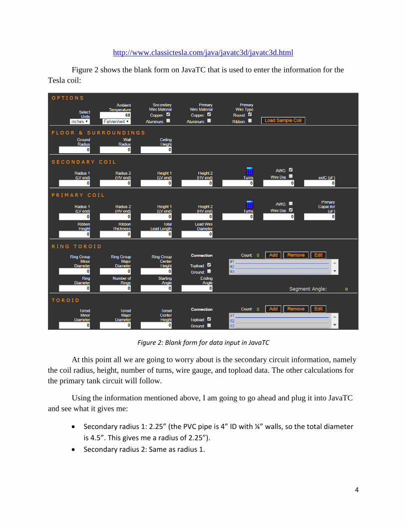
Figure 2 shows the blank form on JavaTC that is used to enter the information for the
Tesla coil:
Figure 2: Blank form for data input in JavaTC
At this point all we are going to worry about is the secondary circuit information, namely
the coil radius, height, number of turns, wire gauge, and topload data. The other calculations for
the primary tank circuit will follow.
Using the information mentioned above, I am going to go ahead and plug it into JavaTC
and see what it gives me:
Secondary radius 1: 2.25” (the PVC pipe is 4” ID with ¼” walls, so the total diameter
is 4.5”. This gives me a radius of 2.25”).
Secondary radius 2: Same as radius 1.
5
Height 1: This is how high off the ground the bottom of your secondary sits. I will
have mine set up on a stand that is 24” tall. Therefore, the height off the ground is
24”.
Height 2: The coil will be 12” tall, so 24” + 12” = 36”.
Since I haven’t wound the coil yet, I don’t have the number of turns and will need to
calculate it. I know that I am using #34 AWG wire, which has a bare wire diameter of
0.0063 inches plus 0.0007 inch thick enamel (JavaTC has a wire diameter calculator,
which I used to obtain these values), giving me a total wire diameter of 0.007 inches.
Therefore, I can calculate the number of turns by dividing 12 inches by 0.007 (the
width of each turn), which comes out to about 1558 turns.
Again, the wire gauge is #34, or 0.007 inches in diameter
My topload is a toroid (donut) shape. The minor diameter is the diameter of the
tubing. In my case it’s 4 inches.
The major diameter is the overall outer diameter of the donut shape. Mine came out to
be 15.75 inches.
The toroid center height is right in the vertical center of the toroid. Since the toroid is
4” tall (determined by the minor diameter), then the center is at 2 inches. The bottom
of my topload is level with the top of my secondary, so add this 2 inches to the height
of the coil (36” + 2”) and you get 38 inches for the height. Make sure to click “add”
to add the topload to the list. If you have more than one topload, then you can repeat
this process and add your other ones. I don’t recommend large or multiple toroids for
most small DRSSTCs though, as it can cause too much loading on the secondary
circuit and you will risk arcing between the primary and secondary coils. This could
destroy your secondary and potentially your driver circuitry as well.
These are the values that are specific to my coil. Every coil will be different. I plug these
values into JavaTC and the output is shown in Figure 3:
6
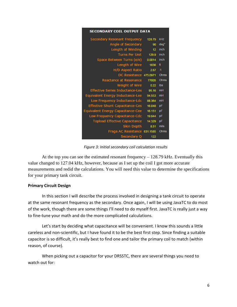
Figure 3: Initial secondary coil calculation results
At the top you can see the estimated resonant frequency – 128.79 kHz. Eventually this
value changed to 127.04 kHz, however, because as I set up the coil I got more accurate
measurements and redid the calculations. You will need this value to determine the specifications
for your primary tank circuit.
Primary Circuit Design
In this section I will describe the process involved in designing a tank circuit to operate
at the same resonant frequency as the secondary. Once again, I will be using JavaTC to do most
of the work, though there are some things I’ll need to do myself first. JavaTC is really just a way
to fine-tune your math and do the more complicated calculations.
Let’s start by deciding what capacitance will be convenient. I know this sounds a little
careless and non-scientific, but I have found it to be the best first step. Since finding a suitable
capacitor is so difficult, it’s really best to find one and tailor the primary coil to match (within
reason, of course).
When picking out a capacitor for your DRSSTC, there are several things you need to
watch out for:
7
Make sure they have a high pulse current. The tank capacitor can see several hundred
to over a thousand amps, or more if you’re running continuous wave ('CW', which
means no interrupter is used), so if the one you pick out can’t handle it, you might
have a small bomb on your hands.
Make sure it is rated for a voltage MUCH higher than your bus voltage (that is, the
voltage you are applying to the bridge, which is generally rectified mains). Some
experienced DRSSTC builders have recommended choosing a capacitor voltage that
is roughly 30x higher than your supplied bus voltage. This is because the voltage on
the primary can ramp up significantly during operation due to the LC resonant circuit.
The capacitor should have a very low dissipation factor. The dissipation factor is the
ratio between the power dissipated by the capacitor’s equivalent series resistance
(ESR) and the power dissipated by the capacitor’s reactance. Otherwise, you will lose
a lot of your energy in the capacitor, potentially damaging it and causing the Tesla
coil to perform poorly.
The capacitor must have a low ESR. A high ESR will lead to excessive internal
heating within the capacitor which will cause it to degrade, and possibly even
explode. Likewise, the equivalent series inductance should also be low.
The best choices are polypropylene film/foil capacitors as they work best at high
frequencies and have a low dissipation factor. I do not recommend ceramic types as
they are generally not very good at Tesla Coil frequencies and will likely be
damaged, regardless of their voltage ratings and capacitance.
The first thing I had to do before looking for capacitors was determine the voltage rating
I’d need. I plan to supply 170VDC to the bridge (rectified 120VAC mains), so that means my
capacitors should be rated for at least Vc = 170v * 30 = 5100 volts AC.
After searching for a while I found a distributor that was selling some MMKP 2uF
530VAC capacitors designed for IGBT snubber applications. Putting 16 of these capacitors in
series gave me a voltage rating of 8480 volts AC, which is plenty for my setup. In general you'll
want to get a capacitor bank that has the correct capacitance and the highest voltage rating
possible. This setup of 16 capacitors in series gave me a total capacitance of 125nF, which is a
very reasonable capacitance for a small DRSSTC. In order to determine what is reasonable you
will need to work ahead a bit to figure out what your primary coil inductance would need to be to
match the resonant frequency of the secondary coil and topload, and if the physical size of the
primary coil would be practical. I probably would not exceed 20 turns on the primary because
that would tend to be bulky and, since the outer coils are further away from the secondary, the
efficiency would likely be lower as well. I generally recommend between 10 and 20 turns,
though that is highly dependent of your particular setup. It is a good goal to aim for, however.
Now that I have a capacitor plan, I can design my primary coil based on the values I
have. To get a general value for the primary inductance required to match the resonance of the
8
secondary, I’m going to use the same formula that I mentioned in the Secondary Coil Design
section:
𝑓 =1
2 ∗ 𝜋 ∗ √𝐿 ∗ 𝐶
Since I know the frequency of the secondary is 128.79 kHz, and I know the capacitance
of the tank capacitor is 125nF, all I need to do is solve for L:
𝐿 =1
4 ∗ 𝐶 ∗ 𝜋2 ∗ 𝑓2
Plug in 125nF for C and 128.79 kHz for f and I get about 12.22uH. Therefore, in order for the
primary to resonate at the same frequency as my secondary, my primary coil will have to have
an inductance of about 12.22uH.
I’m not going to worry about this value too much at this point, as it can generally be
“tuned” later on by “tapping” the coil at different points. All this means is that the outer
connection to the primary coil can be moved around to different points to obtain different
inductances. JavaTC will help take care of any discrepancies later on.
Now that we have a rough estimate of the primary circuit, we can plug it into JavaTC and
see what we get. The values for the secondary will be the same as what I plugged in earlier.
However, we now have the value for the primary capacitor and a value for primary coil
inductance. Note that the primary capacitor is in uF, so I will have to enter 0.125uF instead of
125nF.
Now, the primary is a bit tricky here. Instead of asking for the primary coil inductance, it
asks for the dimensions. Therefore, we’ll have to do a little math. I plan to use ¼” copper tubing
for my primary with 1/8” spacing between each turn. Tubing with this diameter should be able to
handle the high currents reasonably well, and it is fairly easy to obtain from just about any
hardware store. 1/8" spacing between the turns means ¼" center-to-center distance from one turn
to the next (remember the tubing is ¼" diameter as well). I also know that I would like a flat
"pancake" primary coil (simply a flat spiral coil around the base of the secondary coil) to help
prevent primary strikes. So the question now is, how many turns should the primary coil have?
Once again, the number of turns can be adjusted later on by moving the tap point, but getting a
general idea of the number of turns can be very helpful in setting up JavaTC. Knowing that I
want to allow about half an inch between the innermost winding of the primary and the
secondary (to help prevent arc-over), my primary must have a diameter of 5.5”, which means a
radius of 2.75”.
Now the fun part: Calculating the number of turns. I’ll begin with the basic formula for
calculating inductance of a flat pancake primary coil:

9
𝐿 =𝑁2 (
𝐷 + 𝑁(𝑊 + 𝑆)2 )
2
30 (𝐷 + 𝑁(𝑊 + 𝑆)
2 ) − 11𝐷
where L is the inductance in uH, N is the number of turns, D is the inner diameter in inches, S is
the turn spacing in inches, and W is the wire (or tubing) diameter in inches. However, we want to
solve for the number of turns (N), not the inductance (L), so we need to rearrange the formula.
I’ll spare you the gory details and instead I have created an Excel file to approximate the
required turn count. It can be downloaded from the following link:
http://teslaunderground.com/Matt/Primary%20Turns%20Calculator.xlsx
This spreadsheet was put together by a friend of mine to help me out with this problem. It
turns out solving for “N” in the previous equation is not as easy as it sounds, and the formula
becomes very complex. We determined that a lookup table was the best method for estimating
the number of turns required to obtain a given inductance.
Using the Excel sheet I enter 0.125 for S (that is 1/8 inch spacing between the turns.
Note this is not a center-to-center measurement between the windings, but the minimum
distance between them), 0.25 for W (this is the diameter of the tubing I am using), 5.5 for D
(this is the diameter of the innermost winding), and 12.22 (this is the target inductance in
microhenrys in order for the primary tank circuit’s resonant frequency to match that of the
secondary, which I got from JavaTC earlier). In the end, I got N = 6.74 turns.
Now that I have this number, I have a general idea of what to plug into JavaTC. Below
are the values I will be using (which we have determined):
Radius 1: 2.75”
Radius 2: 5.275” (half of Do, calculated by the spreadsheet)
Height 1: 24.125” (this is the height of the stand, 24”, plus half the diameter of the
primary since we’re measuring to the center)
Height 2: Same as Height 1
Turns: 6.74 (calculated by the spreadsheet)
Wire diameter: 0.25”
The input to JavaTC is shown in Figure 4 (don’t forget to put in the values for the secondary coil
and topload again as well):
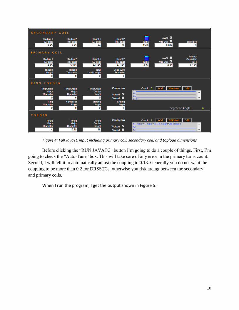
10
Figure 4: Full JavaTC input including primary coil, secondary coil, and topload dimensions
Before clicking the “RUN JAVATC” button I’m going to do a couple of things. First, I’m
going to check the “Auto-Tune” box. This will take care of any error in the primary turns count.
Second, I will tell it to automatically adjust the coupling to 0.13. Generally you do not want the
coupling to be more than 0.2 for DRSSTCs, otherwise you risk arcing between the secondary
and primary coils.
When I run the program, I get the output shown in Figure 5:
11
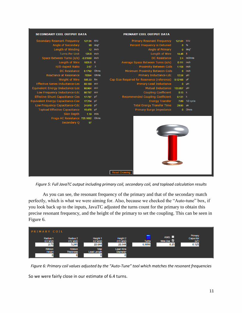
Figure 5: Full JavaTC output including primary coil, secondary coil, and topload calculation results
As you can see, the resonant frequency of the primary and that of the secondary match
perfectly, which is what we were aiming for. Also, because we checked the “Auto-tune” box, if
you look back up to the inputs, JavaTC adjusted the turns count for the primary to obtain this
precise resonant frequency, and the height of the primary to set the coupling. This can be seen in
Figure 6.
Figure 6: Primary coil values adjusted by the “Auto-Tune” tool which matches the resonant frequencies
So we were fairly close in our estimate of 6.4 turns.
12
At this point I think it’s fair to say we have completed the design for the primary and
secondary tank circuits. We have the specifications of both circuits, such as the resonant
frequencies, inductance, coupling coefficient, length of the wire, and so on. Now that we have
designed the actual Tesla coil itself, it’s time to start thinking about how we’re going to drive it.
In the next section we’ll take a look at the schematic and I’ll walk through the theory of
operation.
Schematic
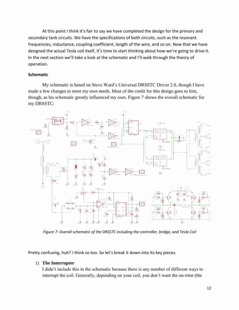
My schematic is based on Steve Ward’s Universal DRSSTC Driver 2.0, though I have
made a few changes to meet my own needs. Most of the credit for this design goes to him,
though, as his schematic greatly influenced my own. Figure 7 shows the overall schematic for
my DRSSTC:
Figure 7: Overall schematic of the DRSSTC including the controller, bridge, and Tesla Coil
Pretty confusing, huh? I think so too. So let’s break it down into its key pieces.
1) The Interrupter
I didn’t include this in the schematic because there is any number of different ways to
interrupt the coil. Generally, depending on your coil, you don’t want the on-time (the
13
amount of time your input signal is HIGH, and thus, the amount of time your coil is
switched on during each high-frequency cycle) to exceed 100uS (though some coils can
handle this without a problem), and generally want the duty cycle to remain around 5% or
lower. A longer on-time and duty cycle will allow excessive current to flow through your
IGBTs and capacitor bank, which could lead to heating and damage to your coil. The link
below is for downloading a calculator program written by Sigurthr (a member at
4hv.org). If you enter your coil’s information (bus voltage, primary tank cap voltage
rating, primary coil inductance, and resonant frequency) it will tell you your maximum
tank current, as well as the maximum allowed pulse width in order to protect your
primary capacitor.
http://teslaunderground.com/Matt/Sigurthr's%20DRSSTC%20Calculator.zip
Possible interrupter ideas range from simple single 555 timer circuits, to more complex
multiple 555 timer designs, to TL494 PWM circuits, and even to microcontroller-based
interrupters. Regardless of the interrupter, however, there is one thing you should pay
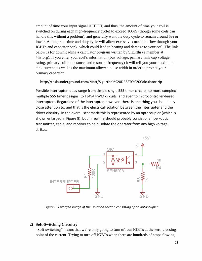
close attention to, and that is the electrical isolation between the interrupter and the
driver circuitry. In the overall schematic this is represented by an optocoupler (which is
shown enlarged in Figure 8), but in real life should probably consist of a fiber-optic
transmitter, cable, and receiver to help isolate the operator from any high voltage
strikes.
Figure 8: Enlarged image of the isolation section consisting of an optocoupler
2) Soft-Switching Circuitry
“Soft-switching” means that we’re only going to turn off our IGBTs at the zero-crossing
point of the current. Trying to turn off IGBTs when there are hundreds of amps flowing
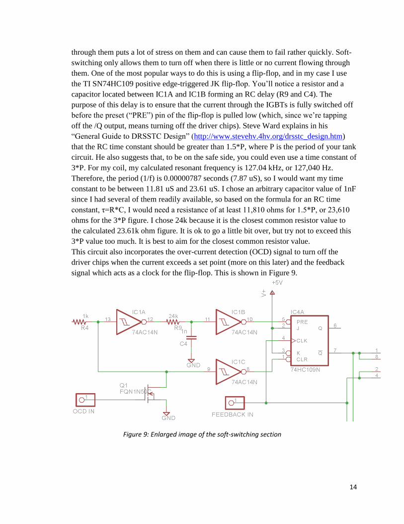
14
through them puts a lot of stress on them and can cause them to fail rather quickly. Soft-
switching only allows them to turn off when there is little or no current flowing through
them. One of the most popular ways to do this is using a flip-flop, and in my case I use
the TI SN74HC109 positive edge-triggered JK flip-flop. You’ll notice a resistor and a
capacitor located between IC1A and IC1B forming an RC delay (R9 and C4). The
purpose of this delay is to ensure that the current through the IGBTs is fully switched off
before the preset (“PRE”) pin of the flip-flop is pulled low (which, since we’re tapping
off the /Q output, means turning off the driver chips). Steve Ward explains in his
“General Guide to DRSSTC Design” (http://www.stevehv.4hv.org/drsstc_design.htm)
that the RC time constant should be greater than 1.5*P, where P is the period of your tank
circuit. He also suggests that, to be on the safe side, you could even use a time constant of
3*P. For my coil, my calculated resonant frequency is 127.04 kHz, or 127,040 Hz.
Therefore, the period (1/f) is 0.00000787 seconds (7.87 uS), so I would want my time
constant to be between 11.81 uS and 23.61 uS. I chose an arbitrary capacitor value of 1nF
since I had several of them readily available, so based on the formula for an RC time
constant, τ=R*C, I would need a resistance of at least 11,810 ohms for 1.5*P, or 23,610
ohms for the 3*P figure. I chose 24k because it is the closest common resistor value to
the calculated 23.61k ohm figure. It is ok to go a little bit over, but try not to exceed this
3*P value too much. It is best to aim for the closest common resistor value.
This circuit also incorporates the over-current detection (OCD) signal to turn off the
driver chips when the current exceeds a set point (more on this later) and the feedback
signal which acts as a clock for the flip-flop. This is shown in Figure 9.
Figure 9: Enlarged image of the soft-switching section
15
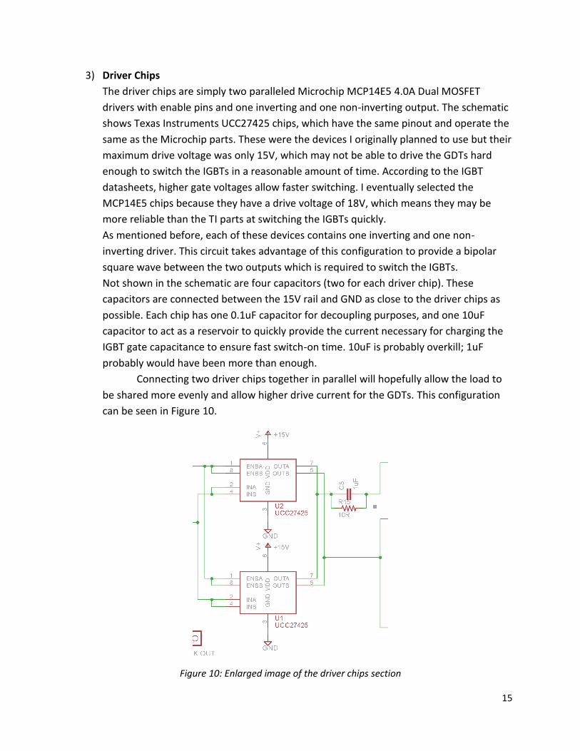
3) Driver Chips
The driver chips are simply two paralleled Microchip MCP14E5 4.0A Dual MOSFET
drivers with enable pins and one inverting and one non-inverting output. The schematic
shows Texas Instruments UCC27425 chips, which have the same pinout and operate the
same as the Microchip parts. These were the devices I originally planned to use but their
maximum drive voltage was only 15V, which may not be able to drive the GDTs hard
enough to switch the IGBTs in a reasonable amount of time. According to the IGBT
datasheets, higher gate voltages allow faster switching. I eventually selected the
MCP14E5 chips because they have a drive voltage of 18V, which means they may be
more reliable than the TI parts at switching the IGBTs quickly.
As mentioned before, each of these devices contains one inverting and one non-
inverting driver. This circuit takes advantage of this configuration to provide a bipolar
square wave between the two outputs which is required to switch the IGBTs.
Not shown in the schematic are four capacitors (two for each driver chip). These
capacitors are connected between the 15V rail and GND as close to the driver chips as
possible. Each chip has one 0.1uF capacitor for decoupling purposes, and one 10uF
capacitor to act as a reservoir to quickly provide the current necessary for charging the
IGBT gate capacitance to ensure fast switch-on time. 10uF is probably overkill; 1uF
probably would have been more than enough.
Connecting two driver chips together in parallel will hopefully allow the load to
be shared more evenly and allow higher drive current for the GDTs. This configuration
can be seen in Figure 10.
Figure 10: Enlarged image of the driver chips section
16
You’ll notice on the output that I have a capacitor in parallel with a resistor on one of
the outputs, in series with the GDT primaries. I eventually added a second capacitor
(0.01uF) in series with the resistor and connected the smaller capacitor and resistor
across the 1uF capacitor. The idea was that the 1uF capacitor would block any DC, which
could cause the GDTs and IGBTs to latch up and cause excessive heating. However, this
capacitor is in the same loop as an inductor (the primary coil of the GDTs), which will
cause “ringing” (unwanted oscillations). In order to avoid this, I added a 10 ohm resistor
in parallel to damp these oscillations. In the case of latch-up, though, this 10 ohm
resistor would pass current, heating up and burning in the process. This actually
happened to me once, which is why I added the 0.01uF capacitor in series with the
resistor. This allows the resistor to damp the oscillations caused by the capacitors and
the GDT primary, but the DC is still blocked by the capacitors.
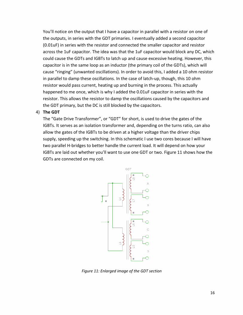
4) The GDT
The “Gate Drive Transformer”, or “GDT” for short, is used to drive the gates of the
IGBTs. It serves as an isolation transformer and, depending on the turns ratio, can also
allow the gates of the IGBTs to be driven at a higher voltage than the driver chips
supply, speeding up the switching. In this schematic I use two cores because I will have
two parallel H-bridges to better handle the current load. It will depend on how your
IGBTs are laid out whether you’ll want to use one GDT or two. Figure 11 shows how the
GDTs are connected on my coil.
Figure 11: Enlarged image of the GDT section
17
Notice that there are two pairs of secondaries, one pair on each of the cores (L5 & L6,
and L7 & L8). The phasing of each transformer is identical, but the two secondaries on
each core are out of phase with each other. This is because of how an H-bridge works;
when one IGBT is on, its complement must be off. In other words, if the high-side
transistor is on, the low-side transistor must be off. By connecting the out-of-phase
secondaries to complimentary IGBTs, it ensures that both of them are not on at the
same time. This phase difference could also be handled by swapping the secondary
connections to the IGBTs, which is what I did in my actual setup.
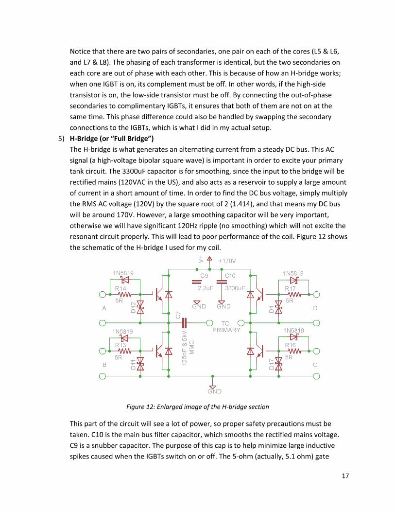
5) H-Bridge (or “Full Bridge”)
The H-bridge is what generates an alternating current from a steady DC bus. This AC
signal (a high-voltage bipolar square wave) is important in order to excite your primary
tank circuit. The 3300uF capacitor is for smoothing, since the input to the bridge will be
rectified mains (120VAC in the US), and also acts as a reservoir to supply a large amount
of current in a short amount of time. In order to find the DC bus voltage, simply multiply
the RMS AC voltage (120V) by the square root of 2 (1.414), and that means my DC bus
will be around 170V. However, a large smoothing capacitor will be very important,
otherwise we will have significant 120Hz ripple (no smoothing) which will not excite the
resonant circuit properly. This will lead to poor performance of the coil. Figure 12 shows
the schematic of the H-bridge I used for my coil.
Figure 12: Enlarged image of the H-bridge section
This part of the circuit will see a lot of power, so proper safety precautions must be
taken. C10 is the main bus filter capacitor, which smooths the rectified mains voltage.
C9 is a snubber capacitor. The purpose of this cap is to help minimize large inductive
spikes caused when the IGBTs switch on or off. The 5-ohm (actually, 5.1 ohm) gate
18
resistors help to minimize ringing on the IGBT gates, the transient voltage suppressor
(TVS) diodes prevent spikes from damaging the IGBT gates and, potentially, the driver
circuitry, and the 1N5819 diodes also help to protect the IGBTs from spikes. It is also
important to note the use of anti-parallel diodes across the emitter and collector of each
of the IGBTs. This also helps minimize large voltage spikes across the collectors and
emitters of the IGBTs when they switch off. Whether the IGBT has a built-in body diode
or not it is important to have an external high-speed diode as well. The body diodes
tend to be slow and will not offer as much protection as a high power, high-speed
Schottky diode would, for example. C7 is the primary resonant tank capacitor. This
capacitor and the primary coil will create a second-order LC circuit that will give us a
resonant frequency determined by the formula we looked at earlier:
𝑓 =1
2 ∗ 𝜋 ∗ √𝐿 ∗ 𝐶
where f is the resonant frequency in Hertz, L is the inductance of the primary in Henrys,
and C is the capacitance of the MMC (“multiple miniature capacitors”, which is a short
way of saying “capacitor bank”) in Farads. The trick is to match this frequency with the
resonant frequency of your secondary coil and topload. Once you do that, you have a
“tuned” Tesla coil.
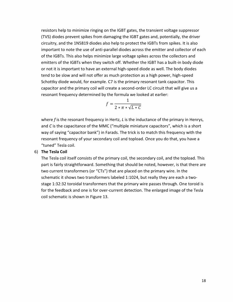
6) The Tesla Coil
The Tesla coil itself consists of the primary coil, the secondary coil, and the topload. This
part is fairly straightforward. Something that should be noted, however, is that there are
two current transformers (or “CTs”) that are placed on the primary wire. In the
schematic it shows two transformers labeled 1:1024, but really they are each a two-
stage 1:32:32 toroidal transformers that the primary wire passes through. One toroid is
for the feedback and one is for over-current detection. The enlarged image of the Tesla
coil schematic is shown in Figure 13.
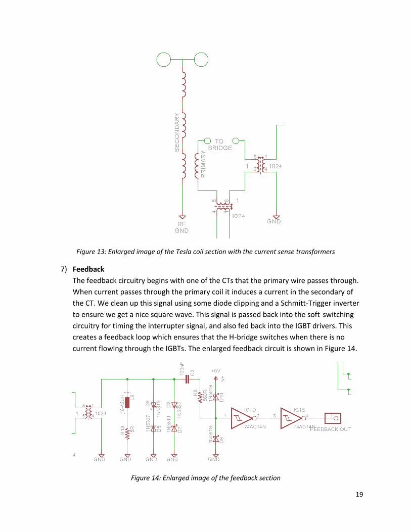
19
Figure 13: Enlarged image of the Tesla coil section with the current sense transformers
7) Feedback
The feedback circuitry begins with one of the CTs that the primary wire passes through.
When current passes through the primary coil it induces a current in the secondary of
the CT. We clean up this signal using some diode clipping and a Schmitt-Trigger inverter
to ensure we get a nice square wave. This signal is passed back into the soft-switching
circuitry for timing the interrupter signal, and also fed back into the IGBT drivers. This
creates a feedback loop which ensures that the H-bridge switches when there is no
current flowing through the IGBTs. The enlarged feedback circuit is shown in Figure 14.
Figure 14: Enlarged image of the feedback section
20
One important thing to note in the feedback circuitry is the variable inductor in series
with a 5 ohm resistor across the output of the transformer. This creates what is called
“phase lead” which, in simple terms, allows the IGBTs to handle higher frequencies.
Recall that we use the flip-flop circuitry to soft-switch the IGBTs. However, large brick-
type IGBTs (like CM300s) generally take a few hundred nanoseconds to switch. While
this may not sound like much, the rise and fall times add up and cause the IGBTs to
switch too late, which leads to them switching with some current flowing through them.
Again, this leads to excessive heating, especially at higher frequencies. The phase lead
allows us to “predict” when the current will cross zero, and make sure the IGBTs
complete their turn-off process right as the current reaches zero. This probably isn’t as
critical for the IGBTs I will be using as I am using smaller ones designed for high
frequencies, but this will be useful in case I ever want to switch to CM300s or CM600s.
By using a variable inductor it will be possible to adjust the phase lead until the actual
switch-off happens right at the zero-current-crossing point.
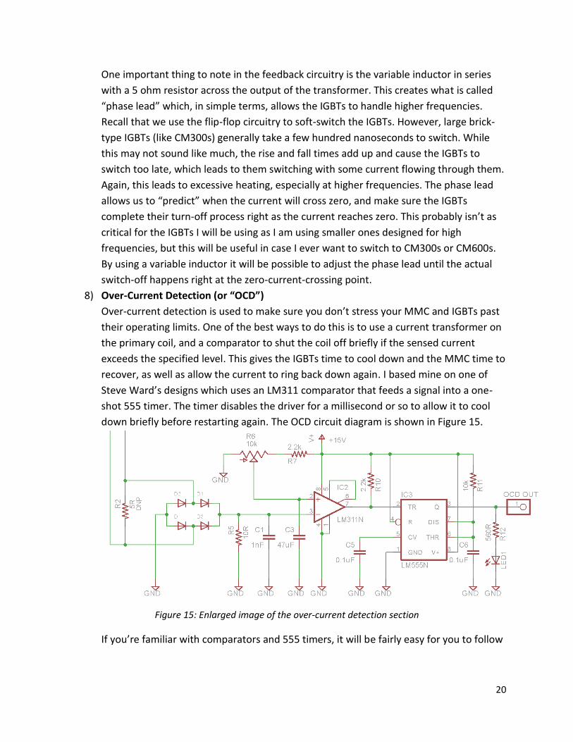
8) Over-Current Detection (or “OCD”)
Over-current detection is used to make sure you don’t stress your MMC and IGBTs past
their operating limits. One of the best ways to do this is to use a current transformer on
the primary coil, and a comparator to shut the coil off briefly if the sensed current
exceeds the specified level. This gives the IGBTs time to cool down and the MMC time to
recover, as well as allow the current to ring back down again. I based mine on one of
Steve Ward’s designs which uses an LM311 comparator that feeds a signal into a one-
shot 555 timer. The timer disables the driver for a millisecond or so to allow it to cool
down briefly before restarting again. The OCD circuit diagram is shown in Figure 15.
Figure 15: Enlarged image of the over-current detection section
If you’re familiar with comparators and 555 timers, it will be fairly easy for you to follow
21
how this works. When the current exceeds the threshold, the voltage on the inverting pin of the
comparator becomes higher than the set voltage on the non-inverting input. This causes the
output of the comparator to be pulled to ground, creating a falling-edge signal on the trigger of
the 555 timer. This causes the output of the 555 to go high for a certain amount of time
determined by the values of C6 and R11. In my case, I use a 10k resistor and a 0.1uF capacitor.
Based on the formula for a one-shot 555 timer:
𝑇 = 1.1 ∗ 𝑅 ∗ 𝐶
these values give me an on-time of 1.1mS. While the 555 output is high, it pulls the input of the
inverter (IC1C) low by an N-Channel MOSFET, and the “CLR” input of the flip-flop is held high.
Since we’re tapping off of the /Q output, then the enable pins of the drivers which are
connected to /Q are held low for that 1.1mS, which means the coil stays off for that amount of
time. I realize there are several inversions here and it may be difficult to follow, but it comes
out correctly in the end.
Interrupter Design
The interrupter is the part of the circuit that turns the Tesla coil on and off at a certain
frequency by disabling the driver circuit multiple times per second. The interrupter is probably
one of the easiest parts to design and build, but is still a critical piece if you designed your coil
to run in non-continuous-wave (“CW”) mode. “Continuous Wave” means that your Tesla coil is
constantly on, which means the output is running at the Tesla coil’s resonant frequency. These
coils tend to be very quiet due to the fact that their operating frequency is well above the range
that the human ear can detect, and since it is not being switched off for part of the cycle, the
current it draws is significantly higher. This can be great for effect, but it puts a lot of strain on
your coil, capacitors, H-bridge, and driver circuitry. Since the IGBTs I will be using really aren’t
designed for very high power I wouldn’t dare run my coil in CW mode as they would surely be
destroyed. The interrupter provides low duty cycle pulses to the H-bridge which significantly
reduces the average current flowing through the transistors.
The Microchip MCP14E5 MOSFET driver chips have an “enable” pin that allows you to
turn their outputs on or off. This is perfect for my DRSSTC since I will be able to have my
interrupter control it directly. If you build a DRSSTC and do not use driver chips that have
enable pins, you can use some AND and NAND gates (for the inverting and non-inverting
drivers) instead, and have one input of each gate connected to your interrupter to give you the
enable/disable control. Just make sure that when the interrupter is off, NEITHER driver is active.
22
Otherwise you will be drawing current when you shouldn’t be, and it can lead to undesired
operation or damage
One of the simplest interrupter designs I have seen to date is a basic 555 timer in
astable mode. When designing an interrupter there are several things you will need to take into
consideration. The main thing you’ll need to know is the maximum on-time that your IGBTs and
capacitors can handle before the average current through them is too high. For this you will
need to look at the datasheets, primarily the graphs. Figure out how your IGBTs, especially, are
affected by temperature, current, and duty cycle. In a previous section I linked to a program
written by Matt Giordano (“Sigurthr” on the 4hv.org forums) that can tell you what your
maximum on-time should be based on the various aspects of your coil. This program is very
useful when designing your interrupter.
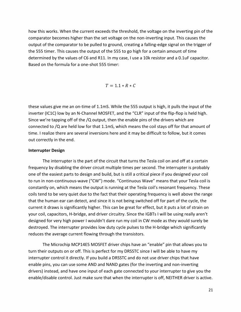
The design shown in Figure 16 is one Steve Ward used in his DRSSTC1, which I looked at
repeatedly (along with the designs for his Universal Driver 2) for reference throughout the
design process. It simply uses a 555 timer and has two adjustments – one for on-time and one
for off-time – which allows the operator to set the pulse width and frequency.
Figure 16: A very basic 555 timer based interrupter
This interrupter design will get you started, though you may eventually decide to design your
own, possibly with a microcontroller, to give you more control of the coil and added features
(for example, audio-modulated “musical” Tesla coils).
Driver Design (GDTs and Driver Circuitry)
In this section we will explore the circuitry used to switch the transistors in the H-bridge.
As mentioned in the Schematic section, I am using two parallel MCP14E5 Dual MOSFET drivers,
each has one inverting driver and one non-inverting driver. When one output is high the other
23
is low, allowing current to flow in one direction, and when the one output is low the other is
high, allowing current to flow in the opposite direction. This is what generates the 15V bipolar
square wave needed for driving the GDTs and the transistors in the H-bridge.
MOSFET drivers are required for this application instead of simply using logic circuitry
not only because of the voltage, but also the current required to drive the GDTs and switch the
IGBTs. If you look at the internal structure of a field-effect transistor (FET), you’ll see that there
is a thin insulating film (usually made of silicon-oxide) between the gate contact and the doped
substrate. You may recognize that this creates a capacitor – two conductive materials separated
by an insulator. As I mentioned before, an IGBT is effectively a MOSFET switching a BJT, so the
device will have a gate capacitance just like any other MOSFET. When running at the high
frequencies of the DRSSTC resonant circuit, charging the gate capacitance (in order to turn on
the IGBT) within a single cycle would require a large amount of current. Looking at the
datasheet for my IGBTs (Fairchild part number FGH60N60UFD), I see that the Gate-Emitter
charge is listed as being 21nC (shown in Figure 17):
Figure 17: Gate-Emitter charge as shown in the IGBT datasheet
Based on the formula:
𝐼 =𝑄
𝑡
where I is the current in Amps, Q is the charge (in Coulombs), and t is the time in seconds, in
order to charge the gate capacitance in, say, 50nS, we would need:
𝐼 =21 ∗ 10−9𝐶
50 ∗ 10−9𝑠= 0.42𝐴 𝑜𝑟 420𝑚𝐴
The driver circuit would need to be able to supply 420mA to switch on the transistor within
50nS. Most logic devices can only source a small fraction of that! Furthermore, some transistors
have even higher gate-emitter charges, or perhaps you need the transistors to switch on even
faster, meaning it could even take several amps to switch on the devices. This is why we use
special MOSFET drivers designed to be able to source this large amount of current.
In order to switch the transistors, it is important to remember that the gate-emitter
voltage on the IGBTs is what determines whether or not they are turned on. Since the collectors
of the top two transistors are connected to 170VDC and the collectors of the lower IGBTs are
connected to the emitters of the upper ones, the timing just wouldn’t work if we only had one
24
wire driving the gate of each IGBT and the other grounded. In order to switch on the top-left
transistor, for example, it would need to have a gate voltage referenced to the source voltage
(in our case, we would want it to be referenced to GND). However, in order to have the top-left
transistor’s gate referenced to ground, the bottom-right transistor would already need to be
switched on, connecting the primary circuit to ground through it. This means that instead of
switching the opposite transistors at the same time (top-left/bottom-right, then top-
right/bottom-left), the bottom transistors would need to turn on first before their
corresponding top transistors could. This would switch the transistors at different times
(bottom-right, then top-left, then bottom-left, then top-right). This would lead to all sorts of
problems.
Therefore, we use a transformer that we refer to as a gate drive transformer, or “GDT”.
Each secondary of the GDT connects directly across the gate and the emitter of its
corresponding transistor, applying the voltage pulse directly across the gate and emitter,
avoiding the need for the low-side transistors to be switched on first. By generating a pulse on
the primary of the GDT, we can get the same (or very similar) pulse on each of the multiple
secondaries which we can use to switch the transistors in the proper order.
Since the bridge has four IGBTs, I’ll need four secondaries on my GDT – one to drive
each gate – and one primary winding for the signal. In full-bridge designs, the preferred method
is to build a pentifilar (5-winding) transformer on a toroidal core. However, before you pick up
just any toroid and start winding, we need to explore why not all toroids will work.
Many toroidal cores are designed for use as chokes and are absolutely lousy at higher
frequencies, as in GDT applications. Instead of acting as a transformer (the primary inducing
current in the secondaries), these cores prevent fast switching and thus a mangled waveform is
generated on the secondaries. Iron cores or iron powder cores are probably the worst types to
use for GDTs as they have a very low permeability and are very lossy. In order for the GDT to
operate correctly it must have a very high permeability, generally >4,000 and preferably
>10,000. Ferrite is a material generally used that has a very high permeability value. These are
ideal for high frequency applications.
When designing a GDT the first thing you’ll want to determine is how many turns you’ll
need. Too few and your core will saturate, giving poor performance. Too many and you’ll have
a high leakage inductance which will also give you poor performance. Let’s start with the
following formula:
𝐵 =𝑉 ∗ 𝑡
𝑁 ∗ 𝐴𝑒
25
B is the flux density in Teslas, V is the voltage at which you’ll be driving your GDT in volts, t is
the on-time of the signal in seconds, N is the number of turns, and 𝐴𝑒 is the cross-sectional area
of the core in square meters. Saturation occurs when the flux density reaches around 0.2
Teslas, so we’ll rearrange the formula to solve for ‘N’, since we’re looking for the minimum
number of turns that we need:
𝑁 =𝑉 ∗ 𝑡
𝐵 ∗ 𝐴𝑒
Let’s plug in our values and see what we get. My controller drives the GDTs with a 15 volt
signal, so that is our V. To get t we must first find the period of our signal. If you’ll recall, back
when we were designing the resonant circuits we determined that my operating frequency will
be about 127.04 kHz. Since period is 1/frequency, that gives us a period of 7.87 uS. However,
we’re not quite done with this yet. Since t is the on-time, we then have to multiply that value by
the duty cycle as well. In this case I’m going to assume 10% (probably the highest duty cycle I’ll
ever run at), so 7.87𝑢𝑆 ∗ 0.1 = 0.787𝑢𝑆. B, we decided earlier, would need to be set to 0.2T to
signify the point of saturation. Finally, we can generally get 𝐴𝑒 from the datasheet of the core.
The 𝐴𝑒 for the toroid cores I ordered from Digikey (part number 495-3868-ND, which are ferrite
toroid cores from EPCOS, part number B64290L0674X038) is stated to be 95.89𝑚𝑚2, or
9.589 ∗ 10−5𝑚2. Plugging that all into the formula we get:
𝑁 =15𝑣 ∗ (0.787 ∗ 10−6)𝑠
0.2𝑇 ∗ (9.589 ∗ 10−5)𝑚2= 0.6 𝑡𝑢𝑟𝑛𝑠
Well, obviously we’re going to want more than 0.6 turns on our GDT, so we shouldn’t have to
worry about saturation. Most DRSSTC coilers wind their GDTs with 8-15 turns, though it often
involves a bit of trial-and-error, as well as some waveform testing using a signal generator and
an oscilloscope. I re-wound my GDTs several times before I got an acceptable waveform.
Something else to watch out for is having mismatched inductances between the secondaries. If
your secondaries aren’t the exact same length, you may get some switching delay that could
cause your coil to perform poorly, and even damage the IGBTs. We will look at our options in
the build portion of this document.
Keep in mind that it is important to keep the windings on the GDT as tight as possible to
the core. Loose winding leads to higher leakage inductance, which will likely cause excessive
ringing with the IGBT gate capacitances, and less efficient signal transference from the primary
to the secondaries. These oscillations have been known to exceed the turn-on voltage of the
transistors, causing them to switch on when they’re supposed to be off. This can lead to
damage. An extremely useful reference for building and testing your GDTs is Richie Burnett’s
gate-drive transformer page, which can be found here:
26
http://www.richieburnett.co.uk/temp/gdt/gdt2.html
That page shows various examples of different waveforms (good and bad), explains the causes
for the bad ones, and offers suggestions for how to improve them.
H-Bridge
The H-bridge, or just “Bridge”, is the part of the circuit that drives the series tank circuit
that is made up of the primary coil and the tank capacitor. The purpose of the bridge is to
generate a high voltage (170VDC) bipolar square wave from the low voltage (15VDC) bipolar
square wave from the GDTs by changing the direction of the current through the primary coil
and tank capacitor repeatedly. This is mainly done via two or four transistors switched in such a
way as to continuously reverse the current in the primary tank circuit. The most common type
of transistor to use is the IGBT. While MOSFETs may work, their losses will be much higher due
to their on-resistance. As current increases, the power increases exponentially as seen in Ohm’s
Law:
𝑃 = 𝐼2 ∗ 𝑅
where P is the power dissipated by the resistance, I is the current flowing through the
resistance, and R is the on-resistance of the MOSFET. On the other hand, IGBTs (Insulated Gate
Bipolar Transistors) are effectively BJTs switched on by a MOSFET, meaning that the collector-
emitter connection acts as a diode, and thus have a constant voltage drop. Therefore the power
dissipation only increases linearly with current:
𝑃 = 𝐼 ∗ 𝑉
where P is the power dissipated by the diode, I is the current, and V is the voltage drop of the C-
E junction. At the currents we’ll be seeing in this Tesla coil application, IGBTs are much more
efficient than MOSFETs, will not heat up as much, and will not be damaged as easily. I plan to
use IGBTs for this project, so when I reference the bridge transistors, those are what I am
referring to.
There are two main methods to drive the primary tank circuit:
A half bridge
A full bridge
The half bridge utilizes two transistors switched alternately and two bus capacitors to create
a voltage across the primary and tank cap that repeatedly switches polarity. The schematic is
shown in Figure 18.
27
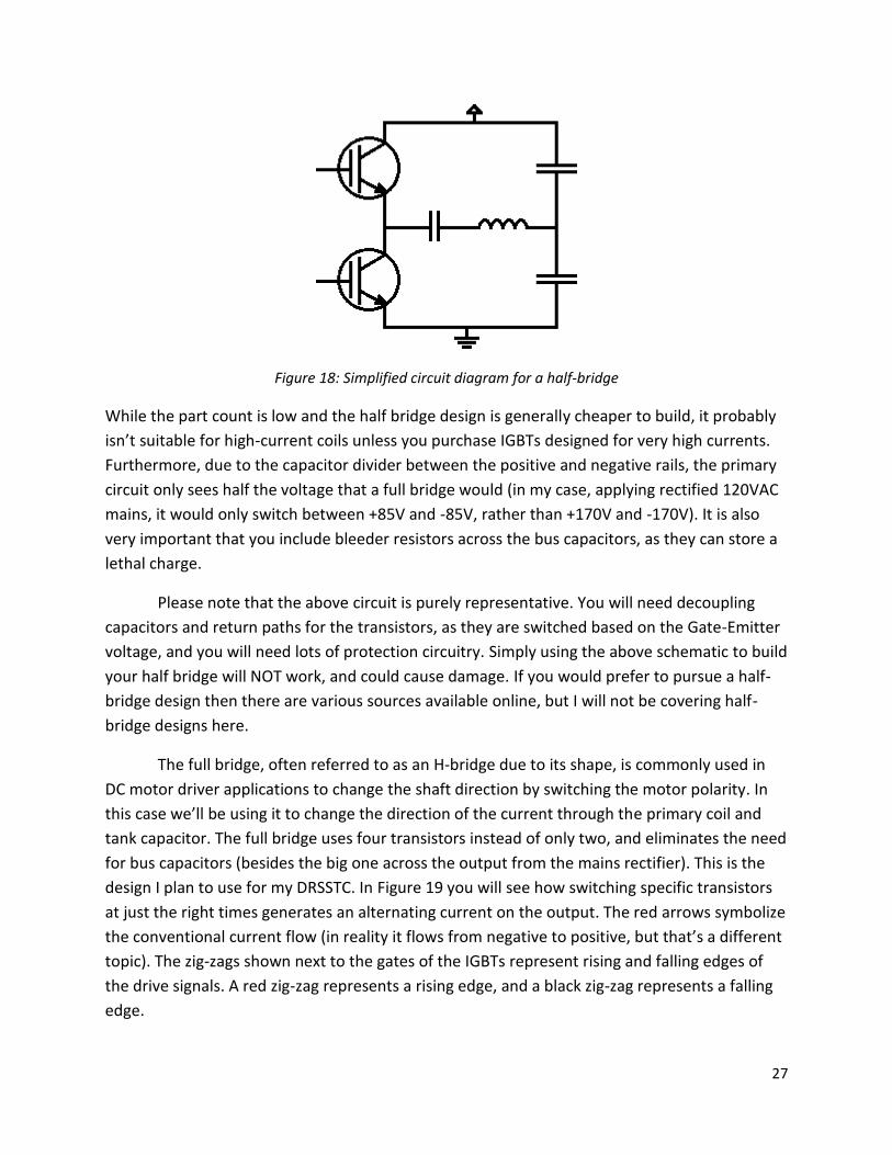
Figure 18: Simplified circuit diagram for a half-bridge
While the part count is low and the half bridge design is generally cheaper to build, it probably
isn’t suitable for high-current coils unless you purchase IGBTs designed for very high currents.
Furthermore, due to the capacitor divider between the positive and negative rails, the primary
circuit only sees half the voltage that a full bridge would (in my case, applying rectified 120VAC
mains, it would only switch between +85V and -85V, rather than +170V and -170V). It is also
very important that you include bleeder resistors across the bus capacitors, as they can store a
lethal charge.
Please note that the above circuit is purely representative. You will need decoupling
capacitors and return paths for the transistors, as they are switched based on the Gate-Emitter
voltage, and you will need lots of protection circuitry. Simply using the above schematic to build
your half bridge will NOT work, and could cause damage. If you would prefer to pursue a half-
bridge design then there are various sources available online, but I will not be covering half-
bridge designs here.
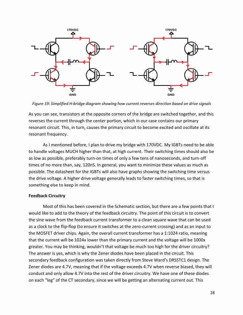
The full bridge, often referred to as an H-bridge due to its shape, is commonly used in
DC motor driver applications to change the shaft direction by switching the motor polarity. In
this case we’ll be using it to change the direction of the current through the primary coil and
tank capacitor. The full bridge uses four transistors instead of only two, and eliminates the need
for bus capacitors (besides the big one across the output from the mains rectifier). This is the
design I plan to use for my DRSSTC. In Figure 19 you will see how switching specific transistors
at just the right times generates an alternating current on the output. The red arrows symbolize
the conventional current flow (in reality it flows from negative to positive, but that’s a different
topic). The zig-zags shown next to the gates of the IGBTs represent rising and falling edges of
the drive signals. A red zig-zag represents a rising edge, and a black zig-zag represents a falling
edge.
28
Figure 19: Simplified H-bridge diagram showing how current reverses direction based on drive signals
As you can see, transistors at the opposite corners of the bridge are switched together, and this
reverses the current through the center portion, which in our case contains our primary
resonant circuit. This, in turn, causes the primary circuit to become excited and oscillate at its
resonant frequency.
As I mentioned before, I plan to drive my bridge with 170VDC. My IGBTs need to be able
to handle voltages MUCH higher than that, at high current. Their switching times should also be
as low as possible, preferably turn-on times of only a few tens of nanoseconds, and turn-off
times of no more than, say, 120nS. In general, you want to minimize these values as much as
possible. The datasheet for the IGBTs will also have graphs showing the switching time versus
the drive voltage. A higher drive voltage generally leads to faster switching times, so that is
something else to keep in mind.
Feedback Circuitry
Most of this has been covered in the Schematic section, but there are a few points that I
would like to add to the theory of the feedback circuitry. The point of this circuit is to convert
the sine wave from the feedback current transformer to a clean square wave that can be used
as a clock to the flip-flop (to ensure it switches at the zero-current crossing) and as an input to
the MOSFET driver chips. Again, the overall current transformer has a 1:1024 ratio, meaning
that the current will be 1024x lower than the primary current and the voltage will be 1000x
greater. You may be thinking, wouldn’t that voltage be much too high for the driver circuitry?
The answer is yes, which is why the Zener diodes have been placed in the circuit. This
secondary feedback configuration was taken directly from Steve Ward’s DRSSTC1 design. The
Zener diodes are 4.7V, meaning that if the voltage exceeds 4.7V when reverse biased, they will
conduct and only allow 4.7V into the rest of the driver circuitry. We have one of these diodes
on each “leg” of the CT secondary, since we will be getting an alternating current out. This
29
clamps the voltage to 0V and 4.7V, which is acceptable for the logic circuitry. However, these
Zener diodes are very slow, which means that when the current on the CT switches direction,
the diodes might become forward-biased which would generate a low-voltage square wave
(around 0.6V max). This would cause timing issues with the driver. Therefore, we also include
an ultra-fast diode front-to-front with each Zener diode to prevent them from ever being
forward-biased. These diodes add another 0.6V drop, which means the logic circuitry will see
between 0V and 5.3V (instead of just 4.7V due to the Zener diodes alone). This clamping forces
the high-amplitude sine wave from the CT to look more like a square wave, which is what we
need. This signal is then passed through a 100nF capacitor to ensure only AC signals can pass
through (again, to prevent latch-up), and then through a 560 ohm resistor to limit the current
into the two Schmitt trigger inverters. To prevent any voltage spikes from entering the logic
circuitry, we add two more ultra-fast diodes to clamp the signal to the + or – rail if it fluctuates
beyond the limits. The Schmitt triggers simply convert our near-square-wave (actually a clipped
sine wave) to a real square wave and cleans it up even further. The output of the second
Schmitt Trigger then feeds into our soft-switching circuitry and into our gate driver chips.
The Build
Now that we’ve covered the basic theory behind how a Tesla coil works, the
components that make up a DRSSTC, and the calculations required for designing the parts, it’s
time to get started with the actual build. Generally you’ll want to do a vast majority of the
planning and design before you begin the building process, though many of the designs may
change if you have difficulty sourcing parts, or trial-and-error suggests you need to make a
change.
Building the Secondary
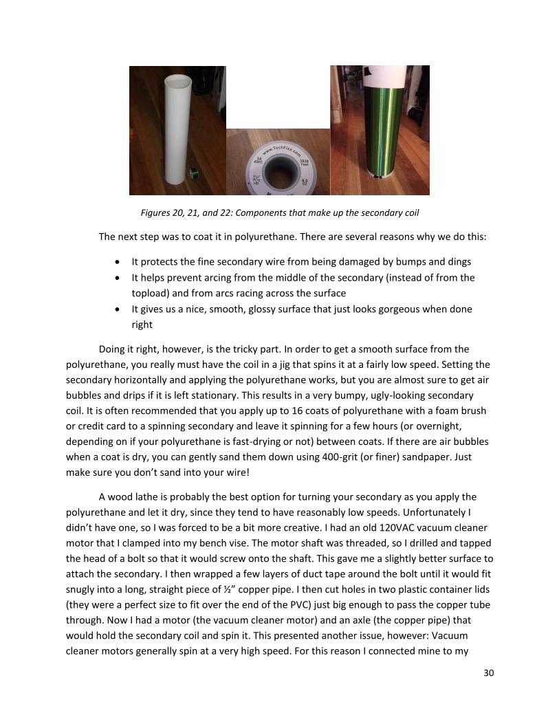
I generally start my Tesla coil builds with the secondary coil. Thankfully most of the
design for my secondary was already done, so all I had to do was put it together. I started with
a 4.5” outer-diameter PVC pipe (white PVC. Don’t use black PVC for Tesla coils, as it contains
traces of carbon which is conductive at higher voltages. This conductivity will likely cause
problems during operation). I bought a few thousand feet of #34 AWG magnet wire and started
winding (by hand). Ten and a quarter hours and over 1800 feet of wire later, I finished winding
my secondary. Most people build jigs to help them wind their secondaries more quickly, but
having limited resources I did it all by hand. The coil is 12 inches tall with approximately 1500
turns, which gave me an inductance of around 87-88mH. Figures 20, 21, and 22 show the PVC
pipe, wire, and completed secondary coil.
30
Figures 20, 21, and 22: Components that make up the secondary coil
The next step was to coat it in polyurethane. There are several reasons why we do this:
It protects the fine secondary wire from being damaged by bumps and dings
It helps prevent arcing from the middle of the secondary (instead of from the
topload) and from arcs racing across the surface
It gives us a nice, smooth, glossy surface that just looks gorgeous when done
right
Doing it right, however, is the tricky part. In order to get a smooth surface from the
polyurethane, you really must have the coil in a jig that spins it at a fairly low speed. Setting the
secondary horizontally and applying the polyurethane works, but you are almost sure to get air
bubbles and drips if it is left stationary. This results in a very bumpy, ugly-looking secondary
coil. It is often recommended that you apply up to 16 coats of polyurethane with a foam brush
or credit card to a spinning secondary and leave it spinning for a few hours (or overnight,
depending on if your polyurethane is fast-drying or not) between coats. If there are air bubbles
when a coat is dry, you can gently sand them down using 400-grit (or finer) sandpaper. Just
make sure you don’t sand into your wire!
A wood lathe is probably the best option for turning your secondary as you apply the
polyurethane and let it dry, since they tend to have reasonably low speeds. Unfortunately I
didn’t have one, so I was forced to be a bit more creative. I had an old 120VAC vacuum cleaner
motor that I clamped into my bench vise. The motor shaft was threaded, so I drilled and tapped
the head of a bolt so that it would screw onto the shaft. This gave me a slightly better surface to
attach the secondary. I then wrapped a few layers of duct tape around the bolt until it would fit
snugly into a long, straight piece of ½” copper pipe. I then cut holes in two plastic container lids
(they were a perfect size to fit over the end of the PVC) just big enough to pass the copper tube
through. Now I had a motor (the vacuum cleaner motor) and an axle (the copper pipe) that
would hold the secondary coil and spin it. This presented another issue, however: Vacuum
cleaner motors generally spin at a very high speed. For this reason I connected mine to my
31
Variac so that I could adjust the voltage being applied to it. Please note this is not a very good
way to do this, and I would strongly recommend setting up a pulley or gear system with a
motor that is easier to control.
I found that running my motor at around 50VAC would spin the secondary at a good
speed, but due to the unexpected load on the motor it would get very warm after only a couple
of minutes. This meant I would not be able to keep it spinning as it dried. For this reason, my
secondary ended up with some air bubbles and drips. However, if I can set up a new jig for
turning the coil I will probably sand it lightly and apply a fresh coat while the secondary is
spinning, which should clean it up nicely.
Building the Topload
My topload is a very simple and cheap one. I took some 4 inch aluminum dryer duct and
bent it into a donut shape. I then used some aluminum foil tape (available at most hardware
stores) to tape the ends together, and then I taped around the entire outside of the duct. This
gave me a nice, reasonably-smooth surface free of holes or sharp ridges that were in the dryer
duct. The final step was to fill the hole in the center of the “donut”. For this I used a 9 inch
aluminum pie plate and taped it in (both from the top and bottom) with the same foil tape I
used to tape over the surface of the toroid. Just like that, my topload was completed.
Ideally one would use a spun aluminum toroid for this purpose. Spun aluminum toroids
are incredibly smooth and prevent premature breakout, and they also look very snazzy.
Unfortunately they are also very expensive, and not in my budget for this coil. Maybe someday.
Building the Capacitor Bank
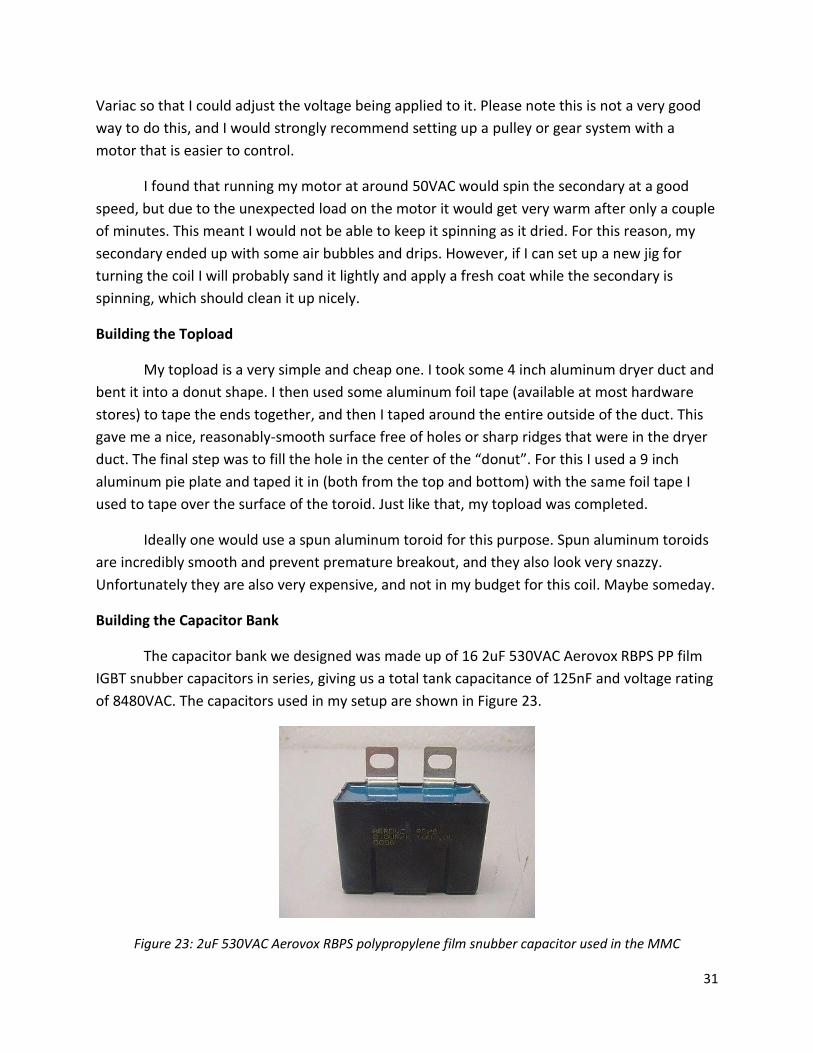
The capacitor bank we designed was made up of 16 2uF 530VAC Aerovox RBPS PP film
IGBT snubber capacitors in series, giving us a total tank capacitance of 125nF and voltage rating
of 8480VAC. The capacitors used in my setup are shown in Figure 23.
Figure 23: 2uF 530VAC Aerovox RBPS polypropylene film snubber capacitor used in the MMC
32
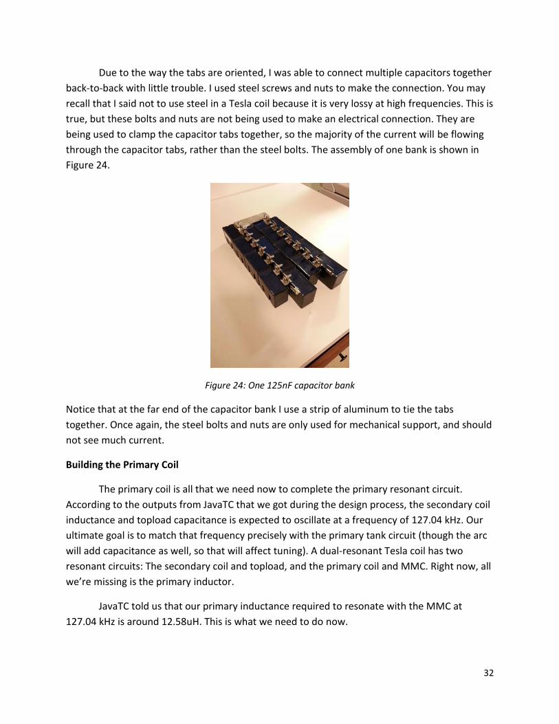
Due to the way the tabs are oriented, I was able to connect multiple capacitors together
back-to-back with little trouble. I used steel screws and nuts to make the connection. You may
recall that I said not to use steel in a Tesla coil because it is very lossy at high frequencies. This is
true, but these bolts and nuts are not being used to make an electrical connection. They are
being used to clamp the capacitor tabs together, so the majority of the current will be flowing
through the capacitor tabs, rather than the steel bolts. The assembly of one bank is shown in
Figure 24.
Figure 24: One 125nF capacitor bank
Notice that at the far end of the capacitor bank I use a strip of aluminum to tie the tabs
together. Once again, the steel bolts and nuts are only used for mechanical support, and should
not see much current.
Building the Primary Coil
The primary coil is all that we need now to complete the primary resonant circuit.
According to the outputs from JavaTC that we got during the design process, the secondary coil
inductance and topload capacitance is expected to oscillate at a frequency of 127.04 kHz. Our
ultimate goal is to match that frequency precisely with the primary tank circuit (though the arc
will add capacitance as well, so that will affect tuning). A dual-resonant Tesla coil has two
resonant circuits: The secondary coil and topload, and the primary coil and MMC. Right now, all
we’re missing is the primary inductor.
JavaTC told us that our primary inductance required to resonate with the MMC at
127.04 kHz is around 12.58uH. This is what we need to do now.
33
My primary coil material of choice for this small coil is ¼” copper tubing. JavaTC stated
that I would need 14.46 feet of it. However, I bought 20 feet (which cost me around $18 at my
local family-owned hardware store) in order to provide plenty of turns for tuning. It is always
good practice to have plenty of turns like this, just in case you decide to make any changes later
on that will require a higher primary coil inductance.
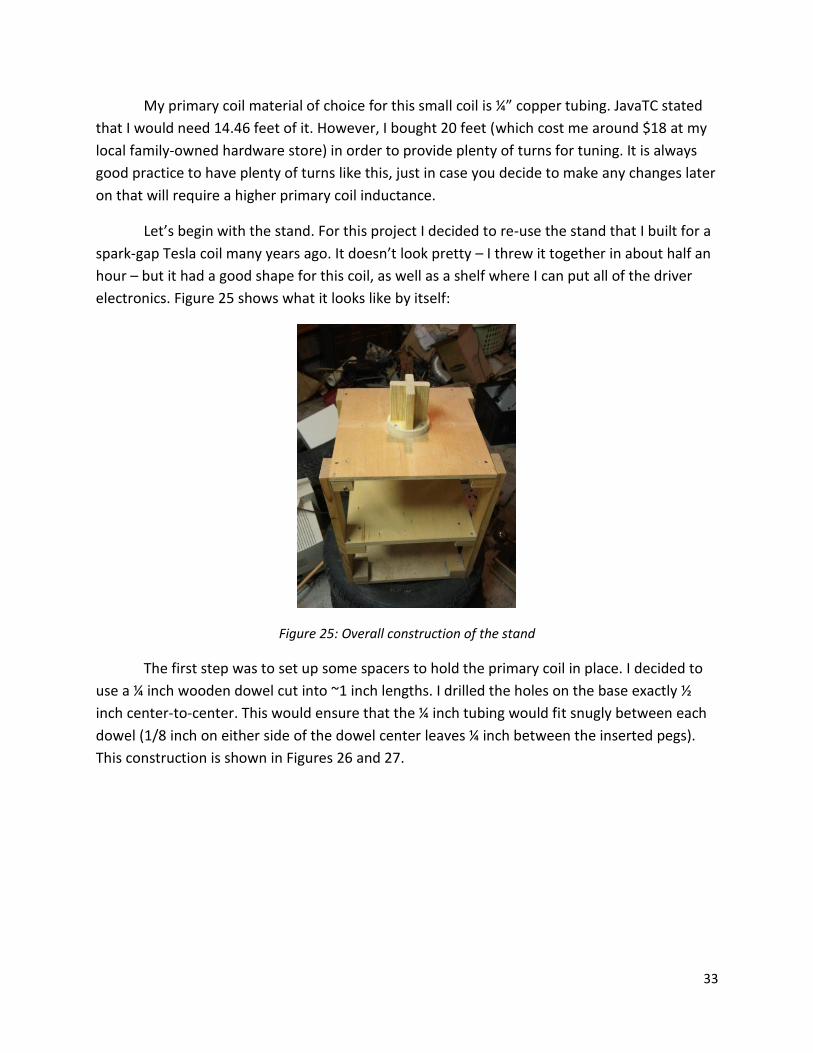
Let’s begin with the stand. For this project I decided to re-use the stand that I built for a
spark-gap Tesla coil many years ago. It doesn’t look pretty – I threw it together in about half an
hour – but it had a good shape for this coil, as well as a shelf where I can put all of the driver
electronics. Figure 25 shows what it looks like by itself:
Figure 25: Overall construction of the stand
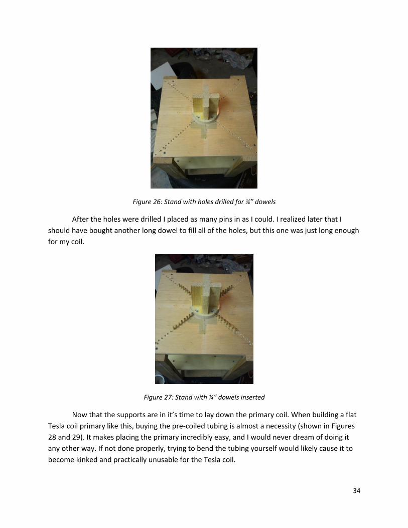
The first step was to set up some spacers to hold the primary coil in place. I decided to
use a ¼ inch wooden dowel cut into ~1 inch lengths. I drilled the holes on the base exactly ½
inch center-to-center. This would ensure that the ¼ inch tubing would fit snugly between each
dowel (1/8 inch on either side of the dowel center leaves ¼ inch between the inserted pegs).
This construction is shown in Figures 26 and 27.
34
Figure 26: Stand with holes drilled for ¼” dowels
After the holes were drilled I placed as many pins in as I could. I realized later that I
should have bought another long dowel to fill all of the holes, but this one was just long enough
for my coil.
Figure 27: Stand with ¼” dowels inserted
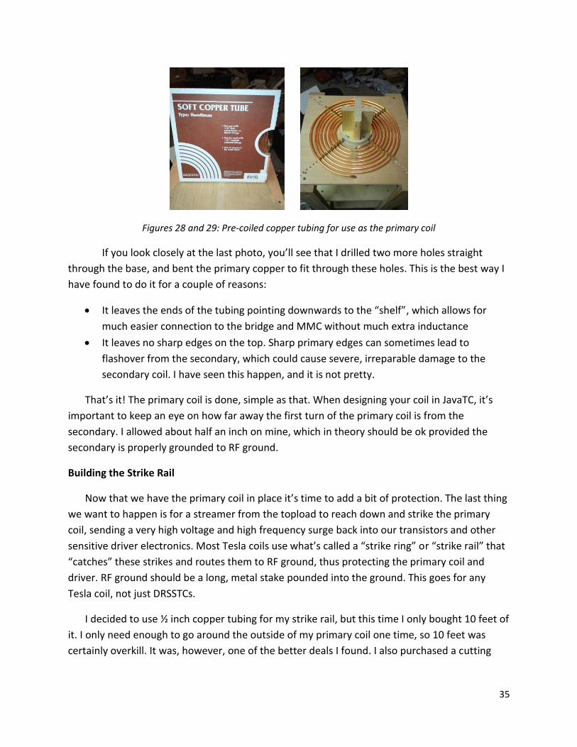
Now that the supports are in it’s time to lay down the primary coil. When building a flat
Tesla coil primary like this, buying the pre-coiled tubing is almost a necessity (shown in Figures
28 and 29). It makes placing the primary incredibly easy, and I would never dream of doing it
any other way. If not done properly, trying to bend the tubing yourself would likely cause it to
become kinked and practically unusable for the Tesla coil.
35
Figures 28 and 29: Pre-coiled copper tubing for use as the primary coil
If you look closely at the last photo, you’ll see that I drilled two more holes straight
through the base, and bent the primary copper to fit through these holes. This is the best way I
have found to do it for a couple of reasons:
It leaves the ends of the tubing pointing downwards to the “shelf”, which allows for
much easier connection to the bridge and MMC without much extra inductance
It leaves no sharp edges on the top. Sharp primary edges can sometimes lead to
flashover from the secondary, which could cause severe, irreparable damage to the
secondary coil. I have seen this happen, and it is not pretty.
That’s it! The primary coil is done, simple as that. When designing your coil in JavaTC, it’s
important to keep an eye on how far away the first turn of the primary coil is from the
secondary. I allowed about half an inch on mine, which in theory should be ok provided the
secondary is properly grounded to RF ground.
Building the Strike Rail
Now that we have the primary coil in place it’s time to add a bit of protection. The last thing
we want to happen is for a streamer from the topload to reach down and strike the primary
coil, sending a very high voltage and high frequency surge back into our transistors and other
sensitive driver electronics. Most Tesla coils use what’s called a “strike ring” or “strike rail” that
“catches” these strikes and routes them to RF ground, thus protecting the primary coil and
driver. RF ground should be a long, metal stake pounded into the ground. This goes for any
Tesla coil, not just DRSSTCs.
I decided to use ½ inch copper tubing for my strike rail, but this time I only bought 10 feet of
it. I only need enough to go around the outside of my primary coil one time, so 10 feet was
certainly overkill. It was, however, one of the better deals I found. I also purchased a cutting
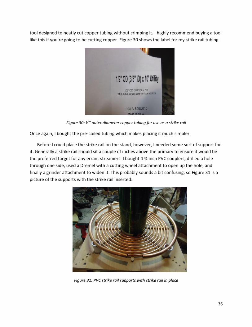
36
tool designed to neatly cut copper tubing without crimping it. I highly recommend buying a tool
like this if you’re going to be cutting copper. Figure 30 shows the label for my strike rail tubing.
Figure 30: ½” outer diameter copper tubing for use as a strike rail
Once again, I bought the pre-coiled tubing which makes placing it much simpler.
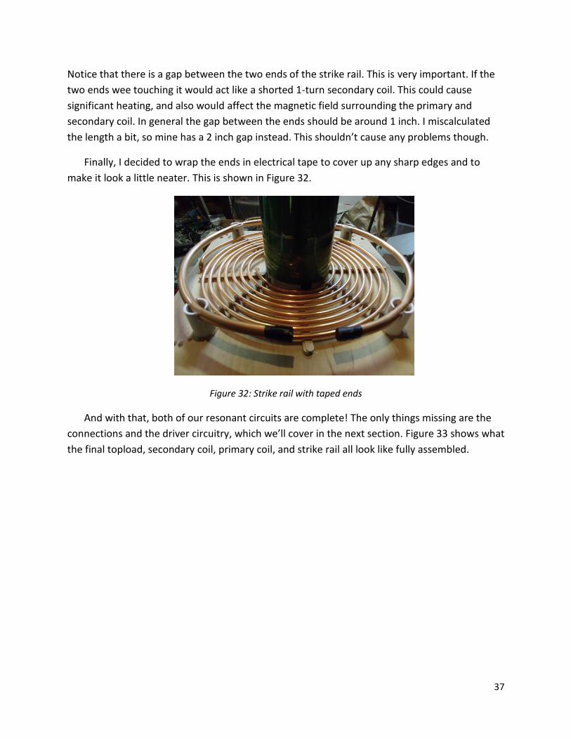
Before I could place the strike rail on the stand, however, I needed some sort of support for
it. Generally a strike rail should sit a couple of inches above the primary to ensure it would be
the preferred target for any errant streamers. I bought 4 ¾ inch PVC couplers, drilled a hole
through one side, used a Dremel with a cutting wheel attachment to open up the hole, and
finally a grinder attachment to widen it. This probably sounds a bit confusing, so Figure 31 is a
picture of the supports with the strike rail inserted:
Figure 31: PVC strike rail supports with strike rail in place
37
Notice that there is a gap between the two ends of the strike rail. This is very important. If the
two ends wee touching it would act like a shorted 1-turn secondary coil. This could cause
significant heating, and also would affect the magnetic field surrounding the primary and
secondary coil. In general the gap between the ends should be around 1 inch. I miscalculated
the length a bit, so mine has a 2 inch gap instead. This shouldn’t cause any problems though.
Finally, I decided to wrap the ends in electrical tape to cover up any sharp edges and to
make it look a little neater. This is shown in Figure 32.
Figure 32: Strike rail with taped ends
And with that, both of our resonant circuits are complete! The only things missing are the
connections and the driver circuitry, which we’ll cover in the next section. Figure 33 shows what
the final topload, secondary coil, primary coil, and strike rail all look like fully assembled.
38
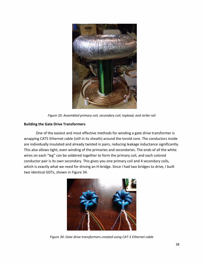
Figure 33: Assembled primary coil, secondary coil, topload, and strike rail
Building the Gate Drive Transformers
One of the easiest and most effective methods for winding a gate drive transformer is
wrapping CAT5 Ethernet cable (still in its sheath) around the toroid core. The conductors inside
are individually insulated and already twisted in pairs, reducing leakage inductance significantly.
This also allows tight, even winding of the primaries and secondaries. The ends of all the white
wires on each “leg” can be soldered together to form the primary coil, and each colored
conductor pair is its own secondary. This gives you one primary coil and 4 secondary coils,
which is exactly what we need for driving an H-bridge. Since I had two bridges to drive, I built
two identical GDTs, shown in Figure 34.
Figure 34: Gate drive transformers created using CAT-5 Ethernet cable
39
Building the Bridge
In order to generate the alternating current required for the primary coil and MMC to
oscillate, you’ll recall we’ll need to create a “Bridge”. Once again, I will be using an H-bridge
configuration for my Tesla coil. This is done using four transistors that, when switched in a
certain way, alternate the direction of current flow through the connected device. It is the same
circuit used in many motor drivers to change the motor direction. In our case it alternates the
direction of current flowing through the primary tank circuit.
The H-bridge was one of the first parts I thought about when starting the design for this
Tesla coil. It is one of the most important parts in the design. While all parts of the Tesla coil are
necessary for its operation, improper construction of the bridge could cause issues ranging
from poor output to severe damage of the device and surrounding property. My original plan
was to use large CM300 IGBT bricks, but I eventually settled on 60N60 IGBTs in TO-247
packages. While these will get significantly hotter than the CM300s due to their small thermal
dissipation area, they will be able to run much faster, which is very important in small, higher-
frequency Tesla coil applications.
I was a bit concerned that the transistors I chose wouldn’t be able to handle the
extremely high currents involved in Tesla coils. The packages were very small and will have
trouble dissipating the heat. I eventually decided that I would double-up the bridges. Using two
bridges in parallel instead of only one will allow them to share the current, thus allowing them
as a whole to handle about twice the current that only one of them could (in theory, assuming
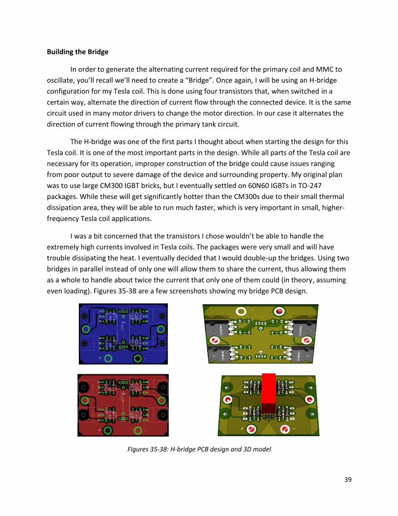
even loading). Figures 35-38 are a few screenshots showing my bridge PCB design.
Figures 35-38: H-bridge PCB design and 3D model
40
Above we have:
Figure 35 (Top-left): Bottom layer of the PCB design
Figure 36 (Top-right): A 3-D rendering (done in Eagle3D) of the bottom of the board (The
IGBT models are backwards though, the backs of the IGBTs should be facing down so
that the thermal tabs mate with the heat sink)
Figure 37 (Bottom-left): Top layer of the PCB design
Figure 38 (Bottom-right): A 3-D rendering (done in Eagle3D) of the top of the board
In these designs I have kept the connections as short as possible and the polygon fills as wide as
possible, to minimize inductance and to allow for better current handling. The schematic I used
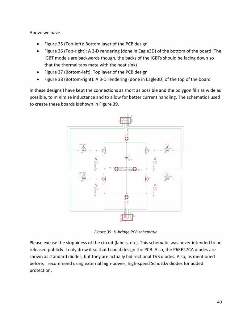
to create these boards is shown in Figure 39.
Figure 39: H-bridge PCB schematic
Please excuse the sloppiness of the circuit (labels, etc). This schematic was never intended to be
released publicly. I only drew it so that I could design the PCB. Also, the P6KE27CA diodes are
shown as standard diodes, but they are actually bidirectional TVS diodes. Also, as mentioned
before, I recommend using external high-power, high-speed Schottky diodes for added
protection.
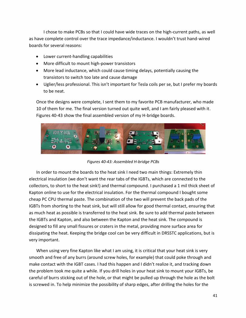
41
I chose to make PCBs so that I could have wide traces on the high-current paths, as well
as have complete control over the trace impedance/inductance. I wouldn’t trust hand-wired
boards for several reasons:
Lower current-handling capabilities
More difficult to mount high-power transistors
More lead inductance, which could cause timing delays, potentially causing the
transistors to switch too late and cause damage
Uglier/less professional. This isn’t important for Tesla coils per se, but I prefer my boards
to be neat.
Once the designs were complete, I sent them to my favorite PCB manufacturer, who made
10 of them for me. The final version turned out quite well, and I am fairly pleased with it.
Figures 40-43 show the final assembled version of my H-bridge boards.
Figures 40-43: Assembled H-bridge PCBs
In order to mount the boards to the heat sink I need two main things: Extremely thin
electrical insulation (we don’t want the rear tabs of the IGBTs, which are connected to the
collectors, to short to the heat sink!) and thermal compound. I purchased a 1 mil thick sheet of
Kapton online to use for the electrical insulation. For the thermal compound I bought some
cheap PC CPU thermal paste. The combination of the two will prevent the back pads of the
IGBTs from shorting to the heat sink, but will still allow for good thermal contact, ensuring that
as much heat as possible is transferred to the heat sink. Be sure to add thermal paste between
the IGBTs and Kapton, and also between the Kapton and the heat sink. The compound is
designed to fill any small fissures or craters in the metal, providing more surface area for
dissipating the heat. Keeping the bridge cool can be very difficult in DRSSTC applications, but is
very important.
When using very fine Kapton like what I am using, it is critical that your heat sink is very
smooth and free of any burrs (around screw holes, for example) that could poke through and
make contact with the IGBT cases. I had this happen and I didn’t realize it, and tracking down
the problem took me quite a while. If you drill holes in your heat sink to mount your IGBTs, be
careful of burrs sticking out of the hole, or that might be pulled up through the hole as the bolt
is screwed in. To help minimize the possibility of sharp edges, after drilling the holes for the
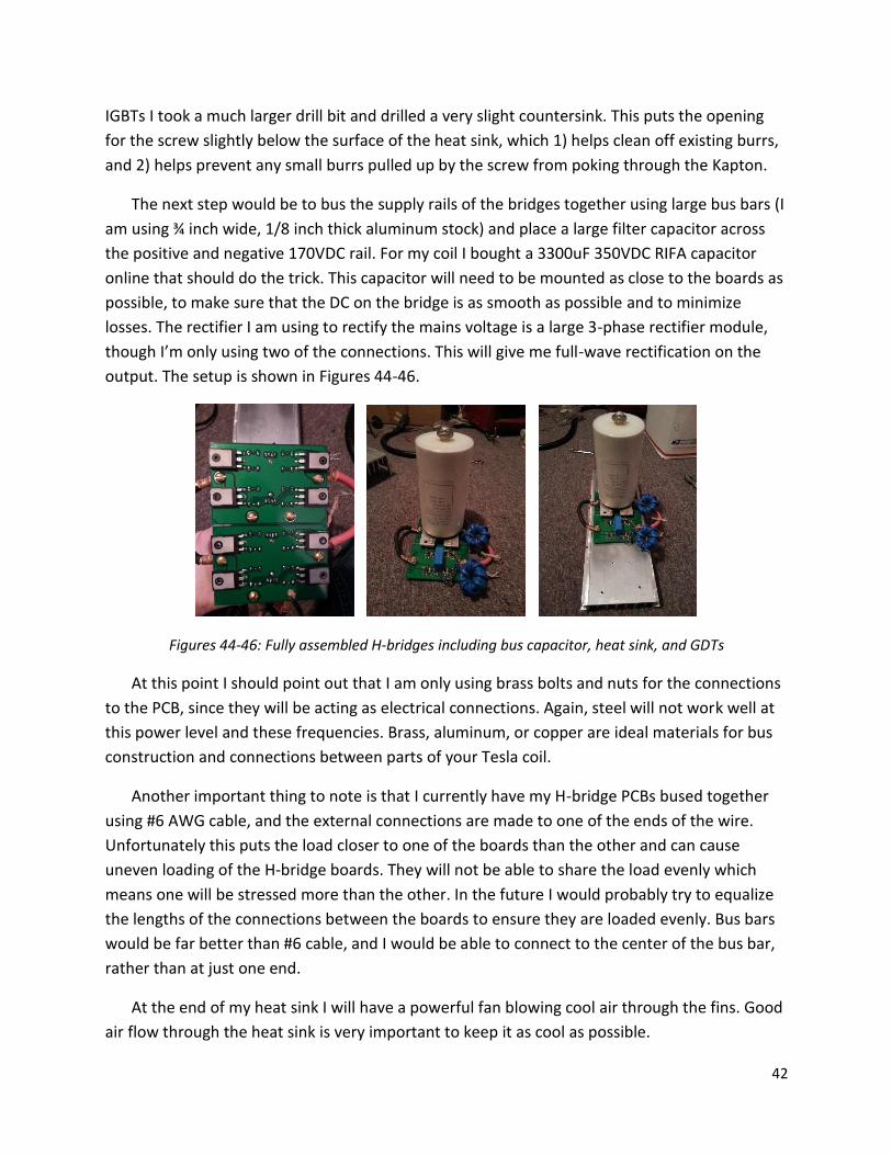
42
IGBTs I took a much larger drill bit and drilled a very slight countersink. This puts the opening
for the screw slightly below the surface of the heat sink, which 1) helps clean off existing burrs,
and 2) helps prevent any small burrs pulled up by the screw from poking through the Kapton.
The next step would be to bus the supply rails of the bridges together using large bus bars (I
am using ¾ inch wide, 1/8 inch thick aluminum stock) and place a large filter capacitor across
the positive and negative 170VDC rail. For my coil I bought a 3300uF 350VDC RIFA capacitor
online that should do the trick. This capacitor will need to be mounted as close to the boards as
possible, to make sure that the DC on the bridge is as smooth as possible and to minimize
losses. The rectifier I am using to rectify the mains voltage is a large 3-phase rectifier module,
though I’m only using two of the connections. This will give me full-wave rectification on the
output. The setup is shown in Figures 44-46.
Figures 44-46: Fully assembled H-bridges including bus capacitor, heat sink, and GDTs
At this point I should point out that I am only using brass bolts and nuts for the connections
to the PCB, since they will be acting as electrical connections. Again, steel will not work well at
this power level and these frequencies. Brass, aluminum, or copper are ideal materials for bus
construction and connections between parts of your Tesla coil.
Another important thing to note is that I currently have my H-bridge PCBs bused together
using #6 AWG cable, and the external connections are made to one of the ends of the wire.
Unfortunately this puts the load closer to one of the boards than the other and can cause
uneven loading of the H-bridge boards. They will not be able to share the load evenly which
means one will be stressed more than the other. In the future I would probably try to equalize
the lengths of the connections between the boards to ensure they are loaded evenly. Bus bars
would be far better than #6 cable, and I would be able to connect to the center of the bus bar,
rather than at just one end.
At the end of my heat sink I will have a powerful fan blowing cool air through the fins. Good
air flow through the heat sink is very important to keep it as cool as possible.
43
Building the Driver
My original driver was handmade on a piece of Veroboard, but I really didn’t like it. The
wiring was very inefficient and overall just looked sloppy. The wire lengths were also not
matched very well which could lead to timing problems. Ultimately I decided to design a new
driver PCB, which I then sent to my favorite manufacturer who made me 10 boards. The
completed PCB is shown in Figure 47.
Figure 47: Vermonster Mini driver PCB (Revision 01)
Assembled it’s still not the prettiest board I’ve done, but at least it looks better than the
hand-wired mess that I built originally.
Figure 48: Assembled Vermonster Mini driver (Revision 01)
Building the Current Sense Transformers
The current transformers, or “CTs”, are used to capture the waveform of the current in
the primary tank circuit and to use it to monitor its amplitude for over-current detection, and to
send a feedback signal to the driver circuitry. The construction of these current transformers is
very simple. I use the same cores as I used for the GDTs and, once again, used Ethernet cable.
44
This time, however, I took it out of its sheath and used Tom Blitch’s method for winding a
1:1024 current transformer. His video can be found here:
https://www.youtube.com/watch?v=HFVR12E2Mek
Each transformer has two cores making up two “stages”, to minimize the number of required
windings. The resulting CTs were then glued together so that they can be placed together
around one of the cables connecting the primary tank circuit to the bridge. The completed
feedback and OCD current transformers are shown in Figures 49 and 50.
Figures 49 and 50: Completed current sense transformers for feedback and over-current detection
Building the Protection Circuitry
One of the worst things that can happen while running a DRSSTC is for the streamer to
strike the primary coil and destroy your transistors. As mentioned before, the strike ring is
designed to “catch” such strikes before they hit the primary, but electricity can be very
unpredictable. For one reason or another it may decide that a jump to the primary coil is an
easier path. Such strikes have been known to destroy IGBTs and other driver circuitry, which we
obviously don’t want. We need to do something to protect the circuitry from primary strikes.
In Steve Ward’s write-up of his DRSSTC4, which can be found at
http://www.stevehv.4hv.org/DRSSTC4.htm , he links to a very helpful diagram he drew that
suggests a method to help prevent damage from primary strikes. This diagram is shown in
Figure 51:
45
Figure 51: Simplified diagram of primary strike protection circuitry and grounding
In this diagram you’ll notice that the RF ground connects to the driver shielding, the H-bridge
heat sink, the strike rail, and the bottom of the secondary coil. It also connects to AC ground.
However, in my setup I will be using a choke between the RF ground and AC ground to increase
the impedance of that branch, hopefully keeping noise out of the mains wiring and forcing it to
be grounded through the long metal rod in the ground. I made the choke out of some Ethernet
wire wrapped around an inductor core from an old ATX power supply. The choke can be seen in
Figure 52:
Figure 52: Choke between RF ground and mains ground to prevent noise from entering the house wiring
Noise on the mains ground is generally frowned upon as it has the potential to damage other
appliances that are plugged in to other power outlets. In reality the choke probably isn’t
required because the impedance of the mains ground path should be much higher than that of
the ground rod, but it still serves as an added safety feature.
46
Also included in Steve’s diagram are two 0.1uF capacitors, one between the positive and
negative DC rail, and one between the negative DC rail and the heat sink (RF ground). I already
had several 0.15uF 940C30P15K-F capacitors from Cornell-Dubilier so I used two of those in the
places shown in the diagram. This setup is shown in Figure 53.
Figure 53: H-bridge assembly with primary strike protection capacitors installed
The main purpose of the 0.15uF capacitor between the negative rail and RF ground (C3) is to
allow the current from the primary strike while the IGBTs are conducting to safely pass through
the IGBTs, through the low impedance of the cap, to RF ground. The capacitor between the
positive and negative rails (C2) is there to pass the current of the strike whenever the reverse
diodes of the IGBTs are conducting. The current from the strike will flow through the reverse
diodes to the positive rail, which is coupled to the negative rail through C2, and thus coupled to
RF ground via C3. In theory this path (regardless of whether it flows through the IGBTs or the
reverse diodes) is a much lower impedance than the path through the insulation of the IGBTs,
which hopefully means the IGBTs will be protected. If the capacitors weren’t there, the chance
of the high voltage punching through the IGBT’s insulation to get to the heat sink (the nearest
RF ground) would be quite high, which would probably destroy the transistors.
The next step was to ground my coil. I used a thin aluminum bar to make the RF ground
connections. I first used a long strip connecting the strike rail to my heat sink. I then cut a
smaller strip that connects to the base of the secondary coil through a spade connector, and
the other end is bolted to the first strip. This shorter bar is also bent around the front to provide
a point where I can connect the grounding rod or cable (shown in Figures 54 and 55).
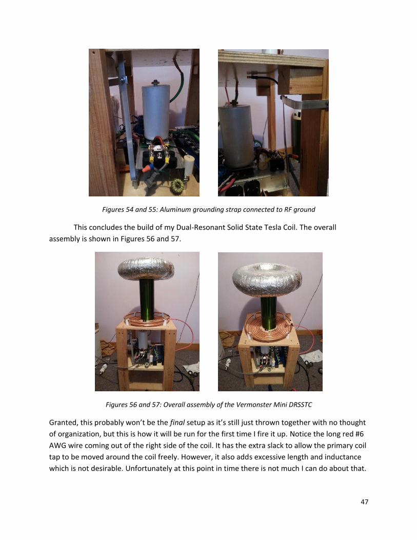
47
Figures 54 and 55: Aluminum grounding strap connected to RF ground
This concludes the build of my Dual-Resonant Solid State Tesla Coil. The overall
assembly is shown in Figures 56 and 57.
Figures 56 and 57: Overall assembly of the Vermonster Mini DRSSTC
Granted, this probably won’t be the final setup as it’s still just thrown together with no thought
of organization, but this is how it will be run for the first time I fire it up. Notice the long red #6
AWG wire coming out of the right side of the coil. It has the extra slack to allow the primary coil
tap to be moved around the coil freely. However, it also adds excessive length and inductance
which is not desirable. Unfortunately at this point in time there is not much I can do about that.
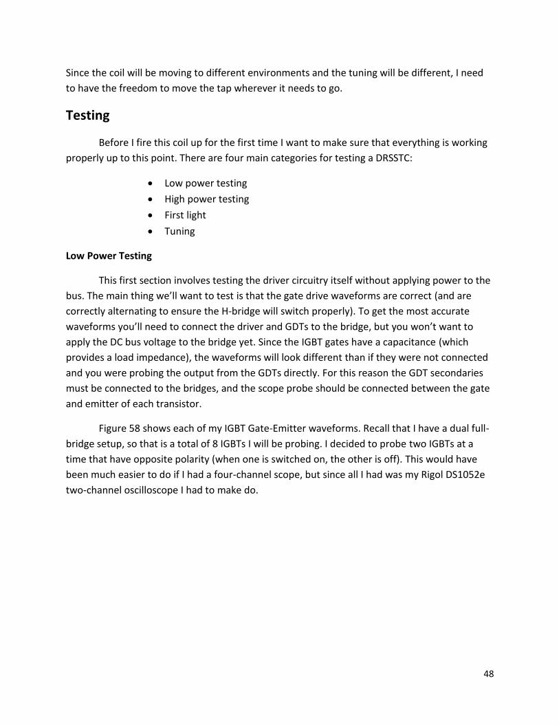
48
Since the coil will be moving to different environments and the tuning will be different, I need
to have the freedom to move the tap wherever it needs to go.
Testing
Before I fire this coil up for the first time I want to make sure that everything is working
properly up to this point. There are four main categories for testing a DRSSTC:
Low power testing
High power testing
First light
Tuning
Low Power Testing
This first section involves testing the driver circuitry itself without applying power to the
bus. The main thing we’ll want to test is that the gate drive waveforms are correct (and are
correctly alternating to ensure the H-bridge will switch properly). To get the most accurate
waveforms you’ll need to connect the driver and GDTs to the bridge, but you won’t want to
apply the DC bus voltage to the bridge yet. Since the IGBT gates have a capacitance (which
provides a load impedance), the waveforms will look different than if they were not connected
and you were probing the output from the GDTs directly. For this reason the GDT secondaries
must be connected to the bridges, and the scope probe should be connected between the gate
and emitter of each transistor.
Figure 58 shows each of my IGBT Gate-Emitter waveforms. Recall that I have a dual full-
bridge setup, so that is a total of 8 IGBTs I will be probing. I decided to probe two IGBTs at a
time that have opposite polarity (when one is switched on, the other is off). This would have
been much easier to do if I had a four-channel scope, but since all I had was my Rigol DS1052e
two-channel oscilloscope I had to make do.
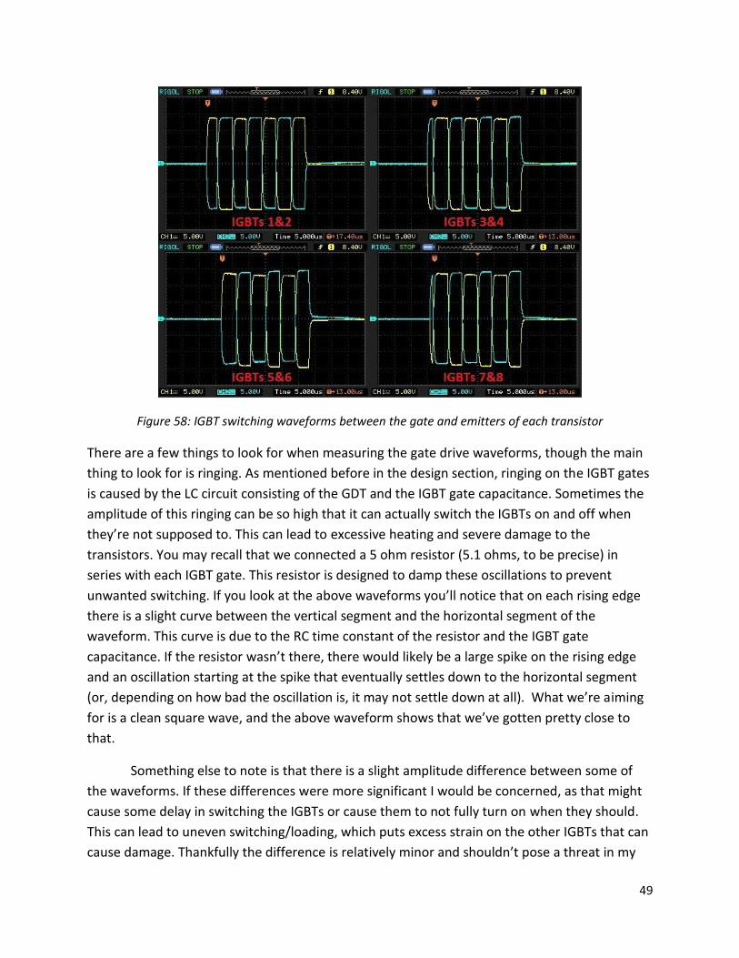
49
Figure 58: IGBT switching waveforms between the gate and emitters of each transistor
There are a few things to look for when measuring the gate drive waveforms, though the main
thing to look for is ringing. As mentioned before in the design section, ringing on the IGBT gates
is caused by the LC circuit consisting of the GDT and the IGBT gate capacitance. Sometimes the
amplitude of this ringing can be so high that it can actually switch the IGBTs on and off when
they’re not supposed to. This can lead to excessive heating and severe damage to the
transistors. You may recall that we connected a 5 ohm resistor (5.1 ohms, to be precise) in
series with each IGBT gate. This resistor is designed to damp these oscillations to prevent
unwanted switching. If you look at the above waveforms you’ll notice that on each rising edge
there is a slight curve between the vertical segment and the horizontal segment of the
waveform. This curve is due to the RC time constant of the resistor and the IGBT gate
capacitance. If the resistor wasn’t there, there would likely be a large spike on the rising edge
and an oscillation starting at the spike that eventually settles down to the horizontal segment
(or, depending on how bad the oscillation is, it may not settle down at all). What we’re aiming
for is a clean square wave, and the above waveform shows that we’ve gotten pretty close to
that.
Something else to note is that there is a slight amplitude difference between some of
the waveforms. If these differences were more significant I would be concerned, as that might
cause some delay in switching the IGBTs or cause them to not fully turn on when they should.
This can lead to uneven switching/loading, which puts excess strain on the other IGBTs that can
cause damage. Thankfully the difference is relatively minor and shouldn’t pose a threat in my
50
case. However, if I were to re-wind my GDTs I would try to be more careful about matching the
lead lengths.
High Power Testing
This is where things get interesting, and potentially hazardous. This is the point where
we apply a voltage to the bus, but leave the secondary coil out of the setup. It is very important
that you use observe all possible safety precautions and consider that, even though there is no
secondary coil, there can still be thousands of volts and hundreds of amps flowing through
certain parts of the circuit. The point where the primary tank capacitor connects to the primary
coil can have a potential of several thousand volts with currents that can be extremely lethal. I
recommend keeping a distance of at least 5 feet when conducting the tests, and preferably
more. This will also reduce the chance of personal harm if a capacitor or transistor explodes,
though 5 feet is definitely on the lower end. I suggest giving yourself as much space as you
possibly can.
There are two waveforms you’re going to want to look for when conducting these tests:
the primary current waveform and the bridge output waveform. In my case, the primary
current waveform is measured by connecting a 10 ohm resistor across the output of one of the
current transformers (ideally you would have a third, separate CT for testing the waveforms)
with the scope + and – leads connected across it. This resistor acts as a shunt that, assuming a
1:1000 turns ratio on the CT, provides a nice 1V/100A output ratio. This figure is very
convenient not only for testing purposes, but also for setting the over-current limiting circuitry
(which also connects to a current transformer with a 10 ohm resistor across it). In reality the
turns ratio is 1:1024, so to get the 1V/100A output ratio the resistor would need to be 10.24
ohms. I ended up using two 5.1 ohm resistors in series giving me 10.2 ohms, which should be
close enough for all intents and purposes.
The Bridge output waveform is measured directly across the output from the bridge
(across the primary coil and tank capacitor series circuit). Before you do this, however, it is very
important that you ensure your oscilloscope is isolated from mains ground. Something some
electronics hobbyists don’t know is that the ground lead of the oscilloscope probe is generally
connected to mains ground through the power cord. If someone tried to connect the probe
across the output of the bridge (each side has a potential of between 0 and 170VDC if powered
from rectified 120VAC mains), the ground lead would connect 170VDC directly to ground,
shorting the scope and potentially damaging it. For this reason an isolation transformer is an
absolute must. Similarly, do not try to probe two different points on your Tesla coil using the
same scope, even if you use different channels. Supposing the oscilloscope is isolated from
mains ground through the isolation transformer, the ground leads of the two channels are still
connected together inside the scope. If you use one probe to measure across the bridge, and
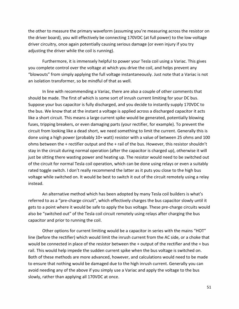
51
the other to measure the primary waveform (assuming you’re measuring across the resistor on
the driver board), you will effectively be connecting 170VDC (at full power) to the low-voltage
driver circuitry, once again potentially causing serious damage (or even injury if you try
adjusting the driver while the coil is running).
Furthermore, it is immensely helpful to power your Tesla coil using a Variac. This gives
you complete control over the voltage at which you drive the coil, and helps prevent any
“blowouts” from simply applying the full voltage instantaneously. Just note that a Variac is not
an isolation transformer, so be mindful of that as well.
In line with recommending a Variac, there are also a couple of other comments that
should be made. The first of which is some sort of inrush current limiting for your DC bus.
Suppose your bus capacitor is fully discharged, and you decide to instantly supply 170VDC to
the bus. We know that at the instant a voltage is applied across a discharged capacitor it acts
like a short circuit. This means a large current spike would be generated, potentially blowing
fuses, tripping breakers, or even damaging parts (your rectifier, for example). To prevent the
circuit from looking like a dead short, we need something to limit the current. Generally this is
done using a high power (probably 10+ watt) resistor with a value of between 25 ohms and 100
ohms between the + rectifier output and the + rail of the bus. However, this resistor shouldn’t
stay in the circuit during normal operation (after the capacitor is charged up), otherwise it will
just be sitting there wasting power and heating up. The resistor would need to be switched out
of the circuit for normal Tesla coil operation, which can be done using relays or even a suitably
rated toggle switch. I don’t really recommend the latter as it puts you close to the high bus
voltage while switched on. It would be best to switch it out of the circuit remotely using a relay
instead.
An alternative method which has been adopted by many Tesla coil builders is what’s
referred to as a “pre-charge circuit”, which effectively charges the bus capacitor slowly until it
gets to a point where it would be safe to apply the bus voltage. These pre-charge circuits would
also be “switched out” of the Tesla coil circuit remotely using relays after charging the bus
capacitor and prior to running the coil.
Other options for current limiting would be a capacitor in series with the mains “HOT”
line (before the rectifier) which would limit the inrush current from the AC side, or a choke that
would be connected in place of the resistor between the + output of the rectifier and the + bus
rail. This would help impede the sudden current spike when the bus voltage is switched on.
Both of these methods are more advanced, however, and calculations would need to be made
to ensure that nothing would be damaged due to the high inrush current. Generally you can
avoid needing any of the above if you simply use a Variac and apply the voltage to the bus
slowly, rather than applying all 170VDC at once.
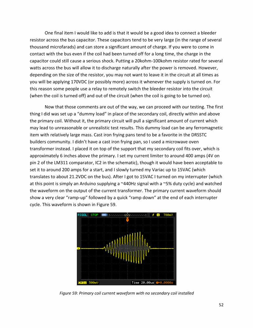
52
One final item I would like to add is that it would be a good idea to connect a bleeder
resistor across the bus capacitor. These capacitors tend to be very large (in the range of several
thousand microfarads) and can store a significant amount of charge. If you were to come in
contact with the bus even if the coil had been turned off for a long time, the charge in the
capacitor could still cause a serious shock. Putting a 20kohm-100kohm resistor rated for several
watts across the bus will allow it to discharge naturally after the power is removed. However,
depending on the size of the resistor, you may not want to leave it in the circuit at all times as
you will be applying 170VDC (or possibly more) across it whenever the supply is turned on. For
this reason some people use a relay to remotely switch the bleeder resistor into the circuit
(when the coil is turned off) and out of the circuit (when the coil is going to be turned on).
Now that those comments are out of the way, we can proceed with our testing. The first
thing I did was set up a “dummy load” in place of the secondary coil, directly within and above
the primary coil. Without it, the primary circuit will pull a significant amount of current which
may lead to unreasonable or unrealistic test results. This dummy load can be any ferromagnetic
item with relatively large mass. Cast iron frying pans tend to be a favorite in the DRSSTC
builders community. I didn’t have a cast iron frying pan, so I used a microwave oven
transformer instead. I placed it on top of the support that my secondary coil fits over, which is
approximately 6 inches above the primary. I set my current limiter to around 400 amps (4V on
pin 2 of the LM311 comparator, IC2 in the schematic), though it would have been acceptable to
set it to around 200 amps for a start, and I slowly turned my Variac up to 15VAC (which
translates to about 21.2VDC on the bus). After I got to 15VAC I turned on my interrupter (which
at this point is simply an Arduino supplying a ~440Hz signal with a ~5% duty cycle) and watched
the waveform on the output of the current transformer. The primary current waveform should
show a very clear “ramp-up” followed by a quick “ramp down” at the end of each interrupter
cycle. This waveform is shown in Figure 59.
Figure 59: Primary coil current waveform with no secondary coil installed
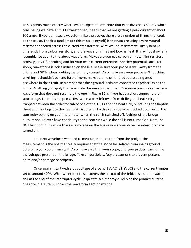
53
This is pretty much exactly what I would expect to see. Note that each division is 500mV which,
considering we have a 1:1000 transformer, means that we are getting a peak current of about
100 amps. If you don’t see a waveform like the above, there are a number of things that could
be the cause. The first (and I made this mistake myself) is that you are using a wire-wound
resistor connected across the current transformer. Wire-wound resistors will likely behave
differently from carbon resistors, and the waveform may not look as neat. It may not show any
resemblance at all to the above waveform. Make sure you use carbon or metal film resistors
across your CT for probing and for your over-current detection. Another potential cause for
sloppy waveforms is noise induced on the line. Make sure your probe is well away from the
bridge and GDTs when probing the primary current. Also make sure your probe isn’t touching
anything it shouldn’t be, and furthermore, make sure no other probes are being used
elsewhere in the circuit. Remember that their ground leads are connected together inside the
scope. Anything you apply to one will also be seen on the other. One more possible cause for a
waveform that does not resemble the one in Figure 59 is if you have a short somewhere on
your bridge. I had this happen at first when a burr left over from drilling the heat sink got
trapped between the collector tab of one of the IGBTs and the heat sink, puncturing the Kapton
sheet and shorting it to the heat sink. Problems like this can usually be tracked down using the
continuity setting on your multimeter when the coil is switched off. Neither of the bridge
outputs should ever have continuity to the heat sink while the coil is not turned on. Note, do
NOT test continuity while there is a voltage on the bus or while your driver or interrupter are
turned on.
The next waveform we need to measure is the output from the bridge. This
measurement is the one that really requires that the scope be isolated from mains ground,
otherwise you could damage it. Also make sure that your scope, and your probes, can handle
the voltages present on the bridge. Take all possible safety precautions to prevent personal
harm and/or damage of property.
Once again, I start with a bus voltage of around 15VAC (21.2VDC) and the current limiter
set to around 400A. What we expect to see across the output of the bridge is a square wave,
and at the end of the interrupter cycle I expect to see it decay quickly as the primary current
rings down. Figure 60 shows the waveform I got on my coil:
54
Figure 60: H-bridge output voltage waveform
If we look more closely at the waveform it doesn’t look much like a square wave except at the
beginning. After the first cycle it starts to slant upwards during the rising portion of the
waveform. This “droop”, as it’s often referred to, can be due to a number of factors. One of the
causes could be the equivalent series resistance (ESR) of the bus capacitor, another could be a
bus capacitance that is too low, and a third could be the position of my dummy load. Ideally my
dummy load would be set within the innermost turn of the primary coil close to the copper
tubing, but since the support is secured in place I simply set the MOT on top of the support.
Proper planning could have prevented this issue and allowed placement of the load closer to
the primary coil. Having the dummy load further away from the primary coil leads to excessive
current draw relative to the applied bus voltage, which leads to “drooping” in the waveform.
While the bridge output waveform is not perfect, it should still work just fine. For future
coils I plan to reduce the size of, or eliminate, the secondary support and find another way to
secure the secondary coil in place. This will allow me to put a dummy load much closer to the
primary, which would help reduce the droop seen in the waveform. I will also look for a
different bus capacitor with a lower ESR and a higher capacitance to minimize the droop.
First Light
“First Light” is a term used to describe a Tesla coil’s first run with a high voltage output.
It is the first run with the secondary placed within the primary coil. Since all the waveforms look
pretty good, I’m comfortable firing it up.
I originally planned to test it for the first time outdoors, with a proper earth ground rod
and everything. However, I decided that if I limit the bus voltage and keep the output low,
connecting to mains ground should be sufficient. I placed the secondary over the form and
connected the ground lead to the RF ground hookup I set up earlier. It is very important that
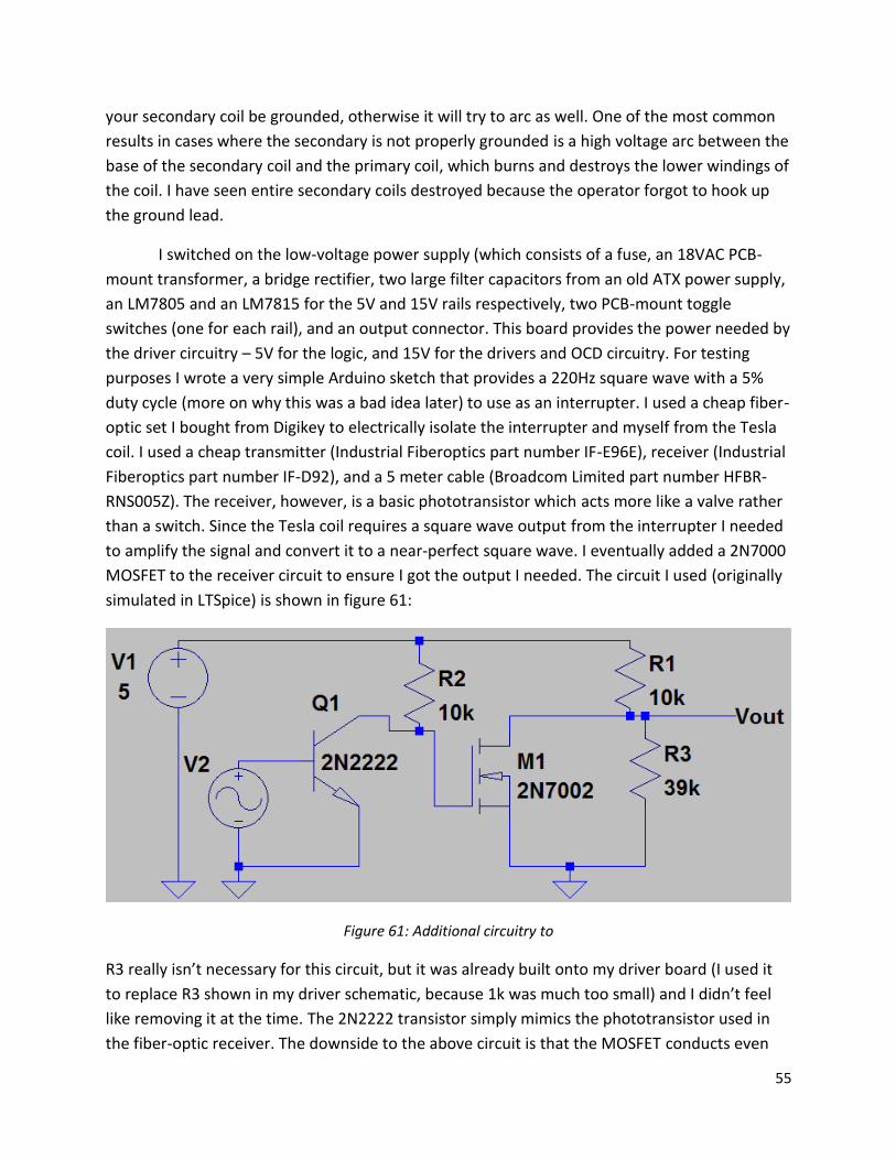
55
your secondary coil be grounded, otherwise it will try to arc as well. One of the most common
results in cases where the secondary is not properly grounded is a high voltage arc between the
base of the secondary coil and the primary coil, which burns and destroys the lower windings of
the coil. I have seen entire secondary coils destroyed because the operator forgot to hook up
the ground lead.
I switched on the low-voltage power supply (which consists of a fuse, an 18VAC PCB-
mount transformer, a bridge rectifier, two large filter capacitors from an old ATX power supply,
an LM7805 and an LM7815 for the 5V and 15V rails respectively, two PCB-mount toggle
switches (one for each rail), and an output connector. This board provides the power needed by
the driver circuitry – 5V for the logic, and 15V for the drivers and OCD circuitry. For testing
purposes I wrote a very simple Arduino sketch that provides a 220Hz square wave with a 5%
duty cycle (more on why this was a bad idea later) to use as an interrupter. I used a cheap fiber-
optic set I bought from Digikey to electrically isolate the interrupter and myself from the Tesla
coil. I used a cheap transmitter (Industrial Fiberoptics part number IF-E96E), receiver (Industrial
Fiberoptics part number IF-D92), and a 5 meter cable (Broadcom Limited part number HFBR-
RNS005Z). The receiver, however, is a basic phototransistor which acts more like a valve rather
than a switch. Since the Tesla coil requires a square wave output from the interrupter I needed
to amplify the signal and convert it to a near-perfect square wave. I eventually added a 2N7000
MOSFET to the receiver circuit to ensure I got the output I needed. The circuit I used (originally
simulated in LTSpice) is shown in figure 61:
Figure 61: Additional circuitry to
R3 really isn’t necessary for this circuit, but it was already built onto my driver board (I used it
to replace R3 shown in my driver schematic, because 1k was much too small) and I didn’t feel
like removing it at the time. The 2N2222 transistor simply mimics the phototransistor used in
the fiber-optic receiver. The downside to the above circuit is that the MOSFET conducts even
56
when the interrupter is turned off. On my next rev of the driver I will be replacing the fiber
optic phototransistor with one that has a TTL output, so I can eliminate all this extra circuitry.
The above circuit will work for testing, however.
After I placed the secondary onto the form and hooked up the ground lead, connected
the low voltage power supply, and set up the interrupter with the fiber optic connection, I was
ready to go. I turned on my Variac, making sure the output was set to 0V, with the interrupter
turned off. I then turned my interrupter on and slowly began to turn up the bus voltage. I began
to hear some buzzing from the breakout point on the topload (a piece of wire I set on top) but
at best I only saw about 1” sparks to the air. If I turned up the bus voltage beyond a certain
level my over-current detector kicked in. This was the telltale sign that my coil was significantly
out of tune, causing it to pull too much current and to have a very poor output.
Tuning
“Tuning” refers to the process of attempting to match the primary resonant frequency
with the secondary resonant frequency. In order to determine the (rough) resonant frequency
of my secondary, I set my function generator to supply a 10V peak-to-peak sine wave and
connected the positive lead to the bottom lead of the secondary coil (RF ground). I left the
negative lead dangling. I then set my scope probe up approximately 1.5 feet from the
secondary coil in a fixed position (to prevent it from swaying). In order to determine the
resonant frequency of my secondary circuit I started at the lowest frequency of my function
generator and slowly increased it. At first nothing really showed up on my scope, but as I
increased the frequency I started seeing a (somewhat sloppy) sine wave appearing on the
scope. As I neared 100 kHz the amplitude and cleanliness of this sine wave increased
dramatically (once again, the probe was not connected to anything) before starting to decrease
again as I continued to increase the frequency on the function generator. The point at which
the amplitude of the waveform on the scope is at its peak shows the resonant frequency of the
secondary (measured by the scope). In my case this test suggested the resonant frequency was
around 103 kHz. This is actually fairly close to my initial estimate of 127 kHz, because being in a
small room, the secondary circuit’s capacitance is slightly higher than calculated which drops
the resonant frequency. This means that in order to match this frequency I would need to
“tune” my primary coil so that it, too, has a lower resonant frequency. Tuning can be done in
two different ways: adjusting the primary tank capacitance or adjusting the primary coil
inductance. I tend to think of it as coarse tuning and fine tuning, respectively. In order to reduce
the resonant frequency I would either need to increase my primary capacitance (add capacitor
strings in parallel with the existing MMC), or increase my primary inductance (tap my primary
coil on one of the outer turns). I decided to move the tap to the last turn to see what effect it
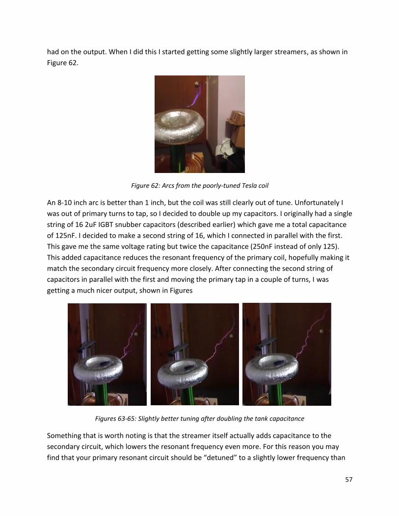
57
had on the output. When I did this I started getting some slightly larger streamers, as shown in
Figure 62.
Figure 62: Arcs from the poorly-tuned Tesla coil
An 8-10 inch arc is better than 1 inch, but the coil was still clearly out of tune. Unfortunately I
was out of primary turns to tap, so I decided to double up my capacitors. I originally had a single
string of 16 2uF IGBT snubber capacitors (described earlier) which gave me a total capacitance
of 125nF. I decided to make a second string of 16, which I connected in parallel with the first.
This gave me the same voltage rating but twice the capacitance (250nF instead of only 125).
This added capacitance reduces the resonant frequency of the primary coil, hopefully making it
match the secondary circuit frequency more closely. After connecting the second string of
capacitors in parallel with the first and moving the primary tap in a couple of turns, I was
getting a much nicer output, shown in Figures
Figures 63-65: Slightly better tuning after doubling the tank capacitance
Something that is worth noting is that the streamer itself actually adds capacitance to the
secondary circuit, which lowers the resonant frequency even more. For this reason you may
find that your primary resonant circuit should be “detuned” to a slightly lower frequency than
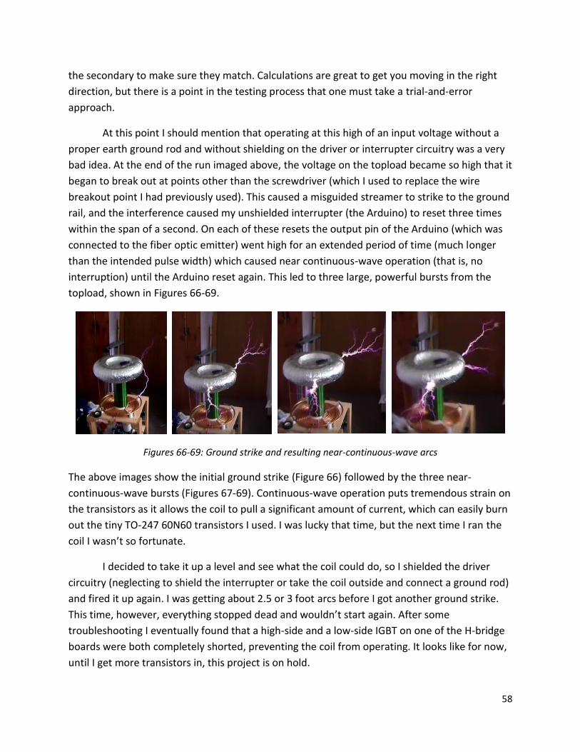
58
the secondary to make sure they match. Calculations are great to get you moving in the right
direction, but there is a point in the testing process that one must take a trial-and-error
approach.
At this point I should mention that operating at this high of an input voltage without a
proper earth ground rod and without shielding on the driver or interrupter circuitry was a very
bad idea. At the end of the run imaged above, the voltage on the topload became so high that it
began to break out at points other than the screwdriver (which I used to replace the wire
breakout point I had previously used). This caused a misguided streamer to strike to the ground
rail, and the interference caused my unshielded interrupter (the Arduino) to reset three times
within the span of a second. On each of these resets the output pin of the Arduino (which was
connected to the fiber optic emitter) went high for an extended period of time (much longer
than the intended pulse width) which caused near continuous-wave operation (that is, no
interruption) until the Arduino reset again. This led to three large, powerful bursts from the
topload, shown in Figures 66-69.
Figures 66-69: Ground strike and resulting near-continuous-wave arcs
The above images show the initial ground strike (Figure 66) followed by the three near-
continuous-wave bursts (Figures 67-69). Continuous-wave operation puts tremendous strain on
the transistors as it allows the coil to pull a significant amount of current, which can easily burn
out the tiny TO-247 60N60 transistors I used. I was lucky that time, but the next time I ran the
coil I wasn’t so fortunate.
I decided to take it up a level and see what the coil could do, so I shielded the driver
circuitry (neglecting to shield the interrupter or take the coil outside and connect a ground rod)
and fired it up again. I was getting about 2.5 or 3 foot arcs before I got another ground strike.
This time, however, everything stopped dead and wouldn’t start again. After some
troubleshooting I eventually found that a high-side and a low-side IGBT on one of the H-bridge
boards were both completely shorted, preventing the coil from operating. It looks like for now,
until I get more transistors in, this project is on hold.
59
Future Plans
1. New Driver
I have been working on a new revision of my driver that adds a few features like
under-voltage lockout (prevents the coil from operating when there’s not enough
drive voltage for the MOSFET drivers), a new fiber optic receiver with a TTL output,
on-board voltage regulation, adjustable drive voltage, and various other minor
changes.
2. New Bridge
TO-247 IGBTs may work ok for small coils, but they’re still pretty wimpy. Eventually I
would like to upgrade to 60N60s in a SOT-227 package which should be able to
handle more power due to their better heat-dissipative capabilities. This will require
an entirely new bridge design. In the meantime I will probably switch to
FGH60N60SMD IGBTs instead of –UFD because they have a higher power handling
capability and a slightly faster switching ability. They also have the same pinout as
the –UFD IGBTs (which I use now) so I would be able to reuse my bridge board if
necessary.
3. Organization
At the moment all of the “guts” of my coil are simply placed on the shelf of my
stand, with no real thought to troubleshooting or organization. I plan to eventually
build a new stand (this time planning the position of all the components to ensure
they’ll fit) and organize the parts in a way that minimizes the lead length.
4. MIDI Control
I plan to develop a MIDI recognition algorithm for a microcontroller that converts
the MIDI signals to signals that can be used to interrupt the Tesla coil. With this
interrupter it would be possible to make the Tesla coil play music through the arcs.
There are certainly more upgrades I would like to make, but they would probably constitute a
whole new Tesla coil.
This has been the process of designing and building my “Vermonster Mini” dual-
resonant solid-state Tesla coil, and hopefully provides a basic framework for designing your
own small DRSSTC as well.