Embed Size (px)
Citation preview

Helsinki Metropolia University of Applied Sciences
Bachelor of Science
Electronics
Thesis
June 19, 2013
Lars Dautermann
Designing a Three Phase Inverter for aPermanent Magnet Synchronous Motor


Abstract
Author Lars DautermannTitle Designing a Three Phase Inverter
for a Permanent Magnet Synchronous Motor
Number of Pages 51 pages + 7 appendicesDate June 19, 2013
Degree Bachelor of Science
Degree Programme European Electrical Engineering
Specialisation option Power electronics
Instructor Arja Ristola, Technology Manager
The motivation for this thesis is to provide a three phase inverter for an electric carin the Formula Student. Designing a inverter is a challenge that requires combinedknowledge in microcontroller programming, pcb layout, electric analysis and theprincipals of how to control a motor.The theory of electrical motors and especially permanent magnet synchronousmotors is shortly introduced. The physical and electrical characteristics werestudied to understand how the motor can be controlled with a three phase inverter.The schematics, the design of drivers and safety features for the switching elementsin the inverter are shown.The software to control the inverter and to communicate with other devices in a carto obtain the information about the desired torque and power is explained.A model of a space vector control in Matlab is simulated.The advantages and disadvantages of different control methods like direct torquecontrol and field oriented control are discussed.
During the study of the thesis two inverter designs were designed. A low voltage, lowpower version to study the concept and a high voltage, high power version for thepractical usage in the car. Due to the limitation of time only the low voltage inverteris built and demonstrated.
Keywords inverter, permanent magnet synchronous motor, mosfet, igbt
Contents
Nomenclature 1
1 Introduction 31.1 Formula Student . . . . . . . . . . . . . . . . . . . . . . . . . . . . 31.2 Metropolia Motorsport . . . . . . . . . . . . . . . . . . . . . . . . . 3
2 Car System Overview 4
3 Theory 53.1 History of Synchronous Motors . . . . . . . . . . . . . . . . . . . . 53.2 Permanent Magnet Motor . . . . . . . . . . . . . . . . . . . . . . . 6
3.2.1 Physical Types of Permant Magnet Motors . . . . . . . . . . 73.2.2 Parameters of PMSM . . . . . . . . . . . . . . . . . . . . . 103.2.3 Dynamic Model of IPMSM - Flux Linkage . . . . . . . . . . 113.2.4 Dynamic Model of IPMSM - Stationary and Synchronous
Frame . . . . . . . . . . . . . . . . . . . . . . . . . . . . . . 123.2.5 Torque Control . . . . . . . . . . . . . . . . . . . . . . . . . 14
3.3 Inverter . . . . . . . . . . . . . . . . . . . . . . . . . . . . . . . . . 153.3.1 Square Wave Conversion . . . . . . . . . . . . . . . . . . . 153.3.2 Modified Sine Wave Conversion . . . . . . . . . . . . . . . 163.3.3 Pure Sine Wave Conversion . . . . . . . . . . . . . . . . . . 173.3.4 Space Vector PWM . . . . . . . . . . . . . . . . . . . . . . 18
3.4 Control loop . . . . . . . . . . . . . . . . . . . . . . . . . . . . . . . 203.4.1 Direct Torque Control . . . . . . . . . . . . . . . . . . . . . 203.4.2 Field Orientated Control . . . . . . . . . . . . . . . . . . . . 203.4.3 Clark-Park Transformation . . . . . . . . . . . . . . . . . . . 23
3.5 Switching Devices . . . . . . . . . . . . . . . . . . . . . . . . . . . 243.5.1 MOSFET . . . . . . . . . . . . . . . . . . . . . . . . . . . . 243.5.2 IGBT . . . . . . . . . . . . . . . . . . . . . . . . . . . . . . . 24
4 Matlab Simulation 27
5 Schematic 285.1 Power Supply Module . . . . . . . . . . . . . . . . . . . . . . . . . 285.2 Microcontroller Modules . . . . . . . . . . . . . . . . . . . . . . . . 295.3 Optocoupler Module . . . . . . . . . . . . . . . . . . . . . . . . . . 305.4 CAN Bus Module . . . . . . . . . . . . . . . . . . . . . . . . . . . . 305.5 Inverter Module . . . . . . . . . . . . . . . . . . . . . . . . . . . . . 315.6 Resolver to Digital Converter Module . . . . . . . . . . . . . . . . . 31
6 Inverter Parts 336.1 Switching Devices . . . . . . . . . . . . . . . . . . . . . . . . . . . 33
6.1.1 MOSFET Driver . . . . . . . . . . . . . . . . . . . . . . . . 346.1.1.1 Bootstrap Driver Calculation . . . . . . . . . . . . 34
6.1.2 IGBT Driver . . . . . . . . . . . . . . . . . . . . . . . . . . . 366.2 Protection . . . . . . . . . . . . . . . . . . . . . . . . . . . . . . . . 38
6.2.1 Short Circuit Protection . . . . . . . . . . . . . . . . . . . . 38

6.2.2 RCD Snubber . . . . . . . . . . . . . . . . . . . . . . . . . . 396.3 Microcontroller . . . . . . . . . . . . . . . . . . . . . . . . . . . . . 406.4 Sensors . . . . . . . . . . . . . . . . . . . . . . . . . . . . . . . . . 40
6.4.1 Temperature Sensors . . . . . . . . . . . . . . . . . . . . . 406.4.2 Current Sensors . . . . . . . . . . . . . . . . . . . . . . . . 406.4.3 Voltage Sensor . . . . . . . . . . . . . . . . . . . . . . . . . 41
7 Measurements 427.1 Voltage Divider Resistance . . . . . . . . . . . . . . . . . . . . . . 427.2 Inverter . . . . . . . . . . . . . . . . . . . . . . . . . . . . . . . . . 44
8 Program 46
9 Summary and Conclusion 47
List of Figures 48
List of Tables 50
Bibliography 51
A Matlab Code 52A.1 Matlab code for square wave generation . . . . . . . . . . . . . . . 52A.2 Matlab code for modified sine wave generation . . . . . . . . . . . 53A.3 Matlab code for pure sine wave generation . . . . . . . . . . . . . 54A.4 Matlab code for space vector PWM . . . . . . . . . . . . . . . . . . 56

1
Nomenclature
λa Flux linkage phase a
λb Flux linkage phase b
λc Flux linkage phase c
λsd, λα Flux linkage in stationary d-axis
λsq, λβ Flux linkage in stationary q-axis
µ0 Permeability of the vacuum
ωr, ωe = P2ωr Rotor speed
ψm Magnetic flux of the permanent magnets
θr, θ = θe = P2θr Rotor flux angle
ea Back EMF phase a
eb Back EMF phase b
ec Back EMF phase c
ia Stationary current phase a
ib Stationary current phase b
ic Stationary current phase c
ied, id D-axis synchronous current
isd, iα D-axis stationary current
ieq, iq Q-axis synchronous current
isq, iβ Q-axis stationary current
kphase Back EMF constant
Ld D-axis synchronous inductance
Lq Q-axis synchronous inductance
Lδ Reluctance inductance component
Labcs Inductance corresponding to the uniform air gap
Lrlc Reluctance matrix
m Space vector sector number
N Number of turns of the d-axis winding
Pe Electric power

2
Te Torque
Ts Switching period
ved, vd D-axis synchronous voltage
vsd, vα D-axis stationary voltage
veq , vq Q-axis synchronous voltage
vsq , vβ Q-axis stationary voltage
Vdc Battery voltage
BLDC Brushless direct current motor
CAN Controller area network
CEMF Counter electromotive eorce
f Frequency
FOC Field oriented control
I2C Inter-integrated circuit
MOSFET Metal oxide semiconductor field effect transistor
P Number of motor poles
PM Permanent magnet
PMSM Permanent magnet synchronous motor
PWM Pulse width modulation
SPI Serial peripheral interface
SVPWM Space vector pulse width modulation

3
1 Introduction
The motivation for this thesis was to provide a three phase inverter for an electriccar in the Formula Student. The Formula Student is an engineering competitionwhere students design and build a car under the rules of the Formula Student.Points can be scored in different engineering and business events throughoutthe competition. Writing this thesis and creating a three phase inverter helps tounderstand the electric car in more detail and gain points in the design event. Aself built and self designed inverter in the car can be better tailored for the desiredpurposes and also helps to assess electromagnetic interference problems betterthat might occur in the car’s communication network.This study is carried out for the Metropolia Motorsport team.
1.1 Formula Student
Figure 1: Formula Student logos
The Formula Student is an engineering com-petition that took place the first time in the USAin 1981. The American competition is the For-mula SAE (Society of Automotive Engineers ).In 2013 there are 11 official competitions inter-nationally: three in the USA, one in Australia,one Brazil, one in Italy, one in the United King-dom, one in Germany, one in Austria, one in Hungary and one in Japan.[6, p. 6][2] The Formula Student in these countries use the same basic set of rules forits competitions which are slightly changed depending on the event. Teams arecreated by students to represent their universities. To the right the logo of theoverall formula student and the logo of the German competition can be seen.
1.2 Metropolia Motorsport
Figure 2: Metropolia Motorsportlogo
The Metropolia Motosport team was formerlyknown as Helsinki Polytechnic Formula Engi-neering Team, which was founded in 2000.The first competition participation was in 2002in Birmingham UK with the car HPF002. In2008 the team changed its name to Metropo-lia Motorsport due to the name change of theuniversity to Helsinki Metropolia University of Applied Sciences. Since then theteam has constructed a car each year and participated in several competitions.

4
In 2013 the team constructed its first fully electric car. In cooperation with ABBthey built their own permanent magnet synchronous motor, which is controlled bya inverter from ABB.[1]In figure 2 the logo of the Metropolia Motorsport team can be seen.
2 Car System Overview
Inverter 1
Inverter 2
Motor 1
Motor 2D
C B
ank
Das
hb
oar
dD
rive
r In
form
atio
n
Ped
als
Torq
ue
Co
ntr
ol
Inp
ut
Controller
Drive Train
Figure 3: System Overview
In figure 3 the top view of the electric car can be seen. The drive train is lo-cated in the rear of the car behind the driver’s seat. At the front of the car thepedals for acceleration and braking can be found.The car has a lot of electrical devices and sensors on board. To control all thosedevices a central control unit is used which runs a self developed software. Thiscontroller is also called main control unit (MCU). The separate electrical systemsin the car communicate by using a CAN bus. The CAN bus was specifically cre-ated to guarantee stable communication in automotive environments. It uses adifferential signal. This helps to prevent coupling of electromagnetic interferences.
For the driver to be able to control the car, the input devices have to be trans-formed into electrical signals. The two front pedals positions are sensed using ahigh precision linear resistor. The steering wheel has an encoder implementedwhich reveals the momentary angle. These signals are evaluated by the main

5
controller. According to the software the acceleration and steering angle infor-mation is calculated into torque and speed demands for the rear wheels. Via theCAN bus this information is send to the inverters in the drive train. The invertersuse the received information to each separately control one motor.Before the car can be set into ready to drive mode a series of safety procedureshave to be executed by the driver.All systems are constantly monitored for failures by software implemented rou-tines as well as hardware implemented safety features.
3 Theory
3.1 History of Synchronous Motors
Synchronous machines were first development during the middle of the 19th cen-tury as single phase generators to supply lighting systems. In the early develop-ment the salient pole rotor motor and the turbo generator formed as the typicaldesign type. Being closely connected with the development of power plants theusage and size of synchronous motors grew with the size of the power plants. Inan industrial manufacturing environment the synchronous motor was used wherea constant speed or usage as a phase shifter was needed.
With the development of frequency inverters the synchronous motor can nowbe used as a speed controlled motor and only recently found its way to new ap-plications ranging from smallest sizes, like watches, phonographs and precisionmechanics up to the biggest sizes and powers used in cement mills, conveyorsand steel mills. [3, p. 289]
The trend is to use high efficiency motors like Permanent Magnet SynchronousMotors (PMSM) in home applications such as refrigerators, air conditioners andwashing machines.A nice side effect is that the efficiency of permanent electric motors can playan important role to reduce greenhouse gases and help reduce the air pollutioncaused by exhausts. The requirement of a clean environment and the reductionof a petroleum dependency has lead to a a paradigm shift. Slowly gasoline en-gines are replaced or at least assisted by electrical machines. In vehicle powertrains more and more vehicles are using hybrid or fully electrical systems. Ongo-ing progress in CPU and power semi conductor performance has made it possibleto easily implement complicated control techniques and algorithms using cost ef-fective components. [4, p. xi]

6
3.2 Permanent Magnet Motor
As seen in Figure 4 AC motors can be divided into asynchronous and synchronousmotors. Like any AC motor asynchronous motors work on the principle of creat-ing a rotating field. [3, p. 170]. Technically asynchronous motors resemble trans-formers. The stator being the primary and the rotor being the secondary side.Asynchronous motors are called asynchronous because the speed of the rotor isless than the speed of the rotating field. This behaviour is called slip.
Synchronous motors use the stator’s and rotor’s magnetic field to lock witheach other in respect to their position leading to a synchronous rotation of therotor with the stator’s magnetic field. The speed of a synchronous motor is n =120∗fP
. If a motor had 4 poles and was supplied with a 50Hz frequency the speedwould be 1500rpm.
Reluctance motors use the effect of attraction experienced when holding amagnet to a magnetisable material like an iron nail. The rotor consisting of amagnetisable material is attracted to the magnetic field created by the stator’scoils.
Permanent magnet motors use the effect of repulsion of equally magnetic po-larized fields experienced when bringing two magnets together with the samepole. The rotor’s magnets are being pushed away by the magnetic field createdin the stator coils.
AC-Motors
Asynchronous Synchronous
Permanent Magnet Motor
BLDC Motor
Surface PM
Motor
Switched Reluctance
Synchronous Reluctance
Reluctance Motor
PMSM
Interior PM
Motor
Squirrel CageInduction Motor
Doubly FedInduction Motor
Figure 4: Taxonomy of AC motors
Permanent magnet motors are classified into two categories based on theshape of their counter clectromotive force (CEMF). According to Faraday’s lawΦB =
∫∫∑
(t)
B(r, t)dA, CEMF is created when a coil rotates in a magnetic field or the

7
other way round a static coil experiences a rotating magnetic field. The changein magnetic flux then induces a voltage according to eb = Kbωr, where Kb is theback EMF constant, and ωr is the rotor angular speed. [4, p. 2]
ea
ea
eb
eb
ec
ec
Time [s]
Vol
tage
[V]
Counter EMF PMSM
(a)
Time [s]
Vol
tage
[V]
Counter EMF BLDC
(b)
Figure 5: (a) Continuous Counter EMF of a PMSM, (b) Trapezoidal Counter EMFof a BLDC
Because the thesis concentrates on a inverter used for a PMSM this type ofpermanent magnet motor will be focused on.
3.2.1 Physical Types of Permant Magnet Motors
In Figure 6 typical PMSM structures are shown. Motors where the PMs are at-tached to the surface of the rotor are called surface PMSM (SPMSM). Motorswhere the PMs are inserted into the rotor are called interior PMSM (IPMSM). Thedifferent arrangement of the permanent magnets leads to different reluctancesand inductances. Because modern PMs have a permeability close to 1 they canbe treated like air regarding the magnetic reluctance. PMs embedded in the rotoralmost always lead to the q-axis synchronous inductance being larger than thed-axis synchronous inductance,
Lq > Ld,
withLd =
µ0N2A
2(g + hm)
andLq =
µ0N2A
2g.

8
Figure 6: Typical PMSM structures: (a) surface magnet, (b) inset magnet, (c) poleshoe rotor, (d) tangentially embedded magnets, (e) radially embedded magnets(flux-concentration), (f) two magnets per pole in the V position, (g) a synchronousreluctance motor equipped with permanent magnets.[8, p. 397]
while PMs on the rotor surface lead to the q-axis synchronous inductancebeing equal to the d-axis synchronous inductance.
Lq = Ld,
withLd = Lq =
µ0N2A
2(g + hm).
With the arrangement in Figure 6(e) a flux concentration can be achieved, forexample an effective flux density of 0,8T using magnets with 0,4T flux density.Though the use of PM mounted on the surface makes better use of the PMs flux,because the magnets in SPMSMs are mounted on the surface the speed rangeand power density is smaller compared to IPMSMs due to the centrifugal forcethat acts upon them and magnet flux leakage, which can even lead to demag-natisation of surface mounted PMs due to the heat created by the losses. [4, p.140],[8]
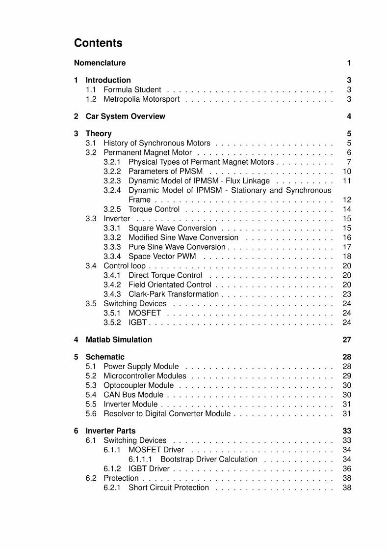
Figure 7 shows the physical structure of the stator and rotor of the motor fromthe Metropolia Motorsport team. It has 24 slots in the stator and 4 magnetic poleson the rotor. The magnets are tangentially embedded. This design was chosento allow speed up to 6000 rpm and and efficient use of power of 8kW-22kW.
9
Stator
North
North
South South
Rotor
Rotor
Slot
Slot
Slot
Slot
Figure 7: Structure of the Metropolia Motorsport’s motor: interior magnet

10
3.2.2 Parameters of PMSM
Given the physical description of a PMSM the most important parameters to de-scribe the motor mathematically are shown in table 1.
Physical representa-tion
Parameter representa-tion
Dimension
Resistance of the mo-tor’s stator winding
RS Ω
D-axis inductance of onemotor phase. This isa transformed value de-rived by the Park trans-formation.
Ld H
Q-axis inductance ofone motor phase. Thisis a transformed valuederived by the Parktransformation.
Lq H
Back EMF constant. KpV srad
Rotor Pole Pair. P 1
Table 1: PMSM parameter overview

11
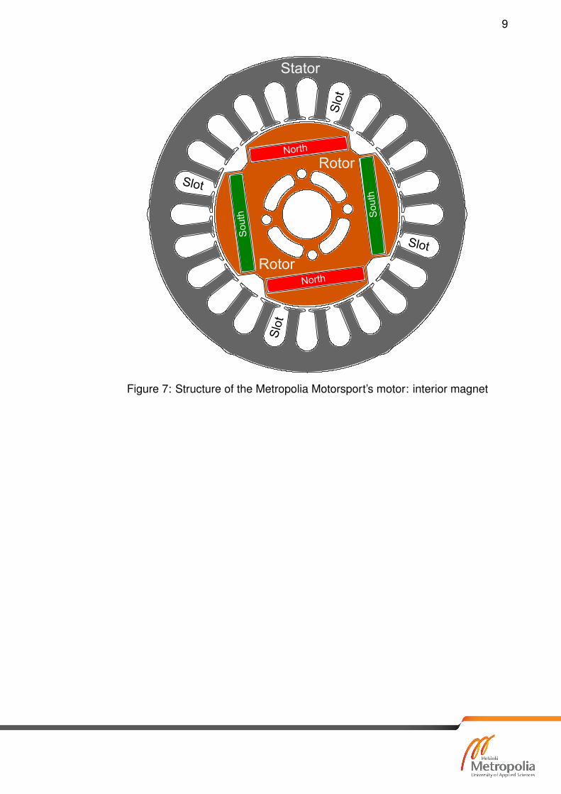
3.2.3 Dynamic Model of IPMSM - Flux Linkage
A simplified equivalent circuit of any AC machine can be seen in Figure 8.The inductance can be divided into stator and rotor inductance. The induc-
tance can be described as [4, p. 149]
Labcs = Labcs − Lrlc(θ),
where
Lrlc(θ) = Lδ
cos 2θ cos(2θ − 2π/3) cos(2θ + 2π/3)
cos(2θ − 2π/3) cos(2θ + 2π/3) cos 2θ
cos(2θ + 2π/3) cos 2θ cos(2θ − 2π/3)
,with
Lδ ≡ µ0N2A
2γ2.
Lδ describes the reluctance component.θ is the rotor angle.µ0 is the permeability of the vacuum.A is the air gap area through which the flux crosses.N is the number of turns of the d-axis winding.γ2 is a positive constant describing the air gap.Lrlc is called reluctance matrix and varies along with the rotor angle.
va
L
ia
ea
ebLib
ec
Libvb
vc
Figure 8: Simplified equivalent circuit of a 3 Phase AC motor.
12
Labcs is the inductance corresponding to the uniform air gap described as
Labcs =
Lms + Lls −1/2Lms −1/2Lms
−1/2Lms Lms + Lls −1/2Lms
−1/2Lms −1/2Lms Lms + Lls
,with
Lms ≡ µ0N2A
2γ0.
γ0 and γ2 are positive constants.The total flux linkage isλaλb
λc
= [Labcs − Lrlc(θ)]
iaibic
+ ψm
cos θ
cos(θ − 2π/3
cos(θ + 2π/3
.
Figure 9: Stationary equivalent circuit of a PMSM (one phase)
3.2.4 Dynamic Model of IPMSM - Stationary and Synchronous Frame
The flux linkage in (3.2.3) is transformed into the stationary d,q frame as[λsdλsq
]=
[Ls − 3/2Lδ cos 2θ −3/2Lδ sin 2θ
−3/2Lδ sin 2θ Ls + 3/2Lδ cos 2θ
][isdisq
]+ ψm
[cos θ
sin θ
].
From this the stationary IPMSM dynamic model is obtained through
vsdq = rsisdq +
d
dtλsdq
An overview of the dynamic models of SPMSM and IPMSM can be seen inTable 2.

13
SPMSM in the stationary frame
ddt
[isdisq
]= rs
Ls
[isdisq
]− ψmωe
Ls
[− sin θecos θe
]+ 1
Ls
[vsdvsq
]IPMSM in the stationary frame[
vsdvsq
]= rs
[isdisq
]+
[Ls − 3
2Lδ cos 2θe −3
2Lδ sin 2θe
−32Lδ sin 2θe Ls + 3
2Lδ cos 2θe
]ddt
[isdisq
]−3ωeLδ
[− sin 2θe cos 2θecos 2θe sin 2θe
] [isdisq
]+ ωeψm
[− sin θecos θe
]SPMSM in the synchronous frame
ddt
[iedieq
]=
[ −rsLs
ωe−ωe − rs
Ls
] [iedieq
]− ψωe
Ls
[01
]+ 1
Ls
[vedveq
]IPMSM in the synchronous frame
ddt
[iedieq
]=
[−rsLd
ωeLq
Ld
−ωe Ld
Lq− rsLs
] [iedieq
]− ψωe
Lq
[01
]+
[1Ldved
1Lqveq
]
Table 2: PMSM dynamic equations[4, p. 154]
Ld = Ls −3
2Lδ
Lq = Ls +3
2Lδ
Ls =3
2Lms + Lls

14
3.2.5 Torque Control
Torque in the rotating frame (synchronous) is calculated as:
Te =3P
4
[ψmi
eq − (Lq − Ld)iedieq
].
ψmieq is the electro-magnetic torque based on the Lorentz force, which is build
by the quadrature current.−(Lq − Ld)iedieq is the reluctance torque caused by the Ld − Lq asymmetry.
Using a lossless model where ved = −ωeLqieq and veq = ωeLdied + ωeψm the total
electric power is
Pe =3P
4ωr(ψmi
eq + (Ld − Lq)iedieq
).
From this the torque equation in the stationary frame can be derived as
Te =3P
4(λsdsi
sq − λsqsisd).
where
λsd = Lsisd −
3
2Lδ(−isd cos 2θe + isq sin 2θe) + ψm cos θe,
λsq = Lsisq −
3
2Lδ(i
sd sin 2θe − isq cos 2θe) + ψm sin θe.

15
3.3 Inverter
There are several methods to convert DC to AC. They differ mainly in their approx-imation to a perfect sinusoidal signal. As one would expect the best approximationyields the best transfer of power to a device that expects a sinusoidal signal. Abetter approximation comes with more complexity and cost. A compromise be-tween functionality, cost and complexity has to be made.In this part the advantages and disadvantages of different conversion methodswill be discussed and evaluated.
3.3.1 Square Wave Conversion
The simplest form of DC to AC conversion is a square wave. As shown in figure 10it uses the full DC voltage and switches between this maximum level at 50% dutycycle. This hard switching could be used for a BLDC as this type of motor expectsa DC signal. For a PMSM it is not desirable because it expects a sinusoidalsignal. The advantages of square wave conversion are its simplicity and low costof components. The disadvantages are high amplitude harmonics (Figure 11)and unsmooth behaviour of devices that expect a sinusoidal signal, which leadsto physical stress.
0 0.2 0.4 0.6 0.8 1 1.2 1.4 1.6 1.8 2
−1
−0.5
0
0.5
1
1.5
Time [s]
Vol
tage
[V]
SquareWave
Figure 10: Square wave conversion
The Matlab code to create figure 10 and 11 can be seen in appendix A.1.

16
0 1 2 3 4 5 6 7 8 9 100
0.2
0.4
0.6
0.8
1
Amplitude Spectrum of SquareWave
Frequency [Hz]
|Vol
tage
[V]|
Figure 11: Square wave amplitude spectrum
3.3.2 Modified Sine Wave Conversion
In figure 12 a modified sine wave conversion can be seen. It is an improvementin comparison to the square wave conversion. Instead of just two levels and a 50% duty cycle it uses three levels. The
0 0.2 0.4 0.6 0.8 1 1.2 1.4 1.6 1.8 2
−1
−0.5
0
0.5
1
Time [s]
Vol
tage
[V]
Modified Sinus Wave
Figure 12: Modified sine wave conversion
The Matlab code to create figure 12 and 13 can be seen in appendix A.2.

17
0 1 2 3 4 5 6 7 8 9 100
0.2
0.4
0.6
0.8
1Amplitude Spectrum of Modified Sine Wave
Frequency [Hz]
|Vol
tage
[V]|
Figure 13: Modified sine wave amplitude spectrum
3.3.3 Pure Sine Wave Conversion
In a pure sine wave conversion, the desired sinusoidal signal is compared againsta sawtooth wave. Whenever the desired sinusoidal signal and the desired valueintersects with the sawtooth sampling frequency a new pulse is started until thesawtooth signal reaches the maximum amplitude. A Matlab generated examplecan be seen in figure 14.
0 0.1 0.2 0.3 0.4 0.5 0.6 0.7 0.8 0.9 1
−1
−0.5
0
0.5
1
Pure Sine Wave PWM switching
Time [s]
|Vol
tage
[V]|
Vdc
Vdc/2
Figure 14: Simulated PWM signal for a pure sine wave
In figure 15 the amplitude spectrum of the pure sine wave PWM signal can beseen. It has components spread across a wide range of frequencies because ofthe changing duty cycles during the modulation.
The Matlab code to create figure 14 and 15 can be seen in appendix A.3.

18
0 10 20 30 40 50 60 70 80 90 1000
0.2
0.4
0.6
0.8
1Amplitude Spectrum of sine wave
Frequency [Hz]
|Vol
tage
[V]|
Figure 15: Simulated PWM signal for a pure sine wave amplitude spectrum
3.3.4 Space Vector PWM
In space vector PWM the different switching states of the inverter are mapped intoa hexagon. The state vectors are placed analog to the abc frame. By doing so thesynchronous voltage vectors can be obtained by their amplitude and angle. Whenthey fall into the designated sector a sequence of vector states is run to synthesizethe desired output voltage. To reduce the computing that has to be done thevalues from the stationary abc frame are transformed into the dq synchronousframe. The voltages ved and veq are calculated in the rotating frame as:
ved = (PI)(ie∗d − ied)− ωLqieq, (3.1)
veq = (PI)(ie∗q − ieq)− ωLdied + ωψm. (3.2)
These values are then transformed back into the stationary α,β frame as seenin figure 16. The maximum rms voltages in space vector PWM that can beachieved are higher than with sinusoidal PWM. This is because of the utilisa-tion of the 3rd harmonic.The maximum rms voltage for sinusoidal PWM is
√3
2·√2· Vdc ≈ 0.612 · Vdc.
The maximum rms voltage for space vector PWM is 1√2· Vdc ≈ 0.707 · Vdc
Because space vector PWM utilizes a higher voltage, more or equal power canbe transferred using less current.
In figure 17 it can be seen how the voltage vector is synthesized. The desiredvoltage vector is Va. The vector V1 and V2 represent the configuration of the upperswitches of the inverter. To create vector Va the switch configuration V1 is switchedon for a proportional time T1 of Va1. Then V2 is switched on for a proportional timeT2 of Va2. The duration of each switch position is calculated from vα and vβ as: [4,p. 278]

19
a
b
c
α
β
(a)
V0(0, 0, 0)
V7(1, 1, 1)
V1(1, 0, 0)
V2(1, 1, 0)V3(0, 1, 0)
V4(0, 1, 1)
V5(0, 0, 1) V6(1, 0, 1)
Sector 1
Sector 2
Sector 3
Sector 4
Sector 5
Sector 6α
β
(b)
Figure 16: Stationary frame of the three phases abc with overlayed stationary α,βframe (a), Space dector diagram (b)
T1 =
√3 · TsVdc
·[sin(
πm
3· vα − cos(
πm
3· vβ]
T2 =
√3 · TsVdc
·[− sin(
π(m− 1)
3· vα − cos(
π(m− 1)
3· vβ].
T0 = Ts − (T1 + T2);
Ts is the the switching period.T0 is the zero vector switching time.m is the number of the sector.Vdc is the battery voltage.
V1(1, 0, 0)
V2(1, 1, 0)
Va
Va1
Va2
Sector 1α
β
Figure 17: Space vector synthesizing

20
3.4 Control loop
To control the speed and torque of a PMSM the frequency and voltage have tobe controlled. Thus the devices to control such a motor are called variable fre-quency drive (VFD). Mainly two different control types are distinguished: scalarcontrol and vector control. Scalar control uses the effect of changing the operat-ing parameters such as voltage and frequency to drive the motor at different setsof characteristic curve families. It is called scalar control because it scales theoperating parameters. [9, p. 671]Vector control dynamically controls the motor’s torque directly by observing themotor’s current and keeping the magnitude of the instantaneous magnetizing cur-rent space vector constant so that the rotor flux linkage remains constant.[9, p.645] It is called vector control because it analysis voltage, current and magneticflux based on their vector representation. Two types of vector control, directtorque control (DTC) and field oriented control (FOC), are discussed in moredetail in the following section.
3.4.1 Direct Torque Control
Direct torque control uses the measurement of voltage and current to calculateand estimate the magnetic flux and torque. It can be divided into direct self-control(DSC) and space vector modulation (SVM).
3.4.2 Field Orientated Control
The overall control loop looks similar to figure 18. The torque is controlled by thequadrature current (iq) of the rotor. The current component id does not need tobe controlled. id is normally used to create the flux of the excitation circuit. In aPMSM this flux is constantly present because of the magnets. id can be used toinduce field weakening.As seen in figure 18 the three phase current are measured with an ADC (analogto digital inverter) of a microcontroller. This information is then transformed fromthe stationary three phase stator frame into the rotating rotor frame. Further thisinformation is subtracted from the desired current. A PI controller regulates howmuch the current has to be increased or decreased. This is then calculated intothe corresponding voltage values. After an inverse park transformation from therotating dq frame into the stationary αβ frame the appropriate switching sequenceis executed.

21
Figure 18: Control loop overview
In a more compact way it can be said that field oriented control is the tech-nique used to achieve the decoupled control of torque and flux by transformingthe stator current quantities (phase currents) from the stationary reference frameto torque and flux producing currents components in the rotating (synchronous)reference frame(Figure 19).[7]
A comparison overview between DTC and FOC can be seen in table 3 [10].

22
Comparison property DTC FOC
Dynamic response totorque
Very fast Fast
Coordinates referenceframe
alpha, beta (stator) d, q (rotor)
Low speed (¡ 5% ofnominal) behavior
Requires speed sensorfor continuous braking
Good with position orspeed sensor
Controlled variables torque & stator flux rotor flux, torque currentiq & rotor flux current idvector components
Steady-state torque/cur-rent/flux ripple & distor-tion
Low (requires high qual-ity current sensors)
Low
Parameter sensitivity,sensorless
Stator resistance d, q inductances, rotorresistance
Parameter sensitivity,closed-loop
d, q inductances, flux(near zero speed only)
d, q inductances, rotorresistance
Rotor position measure-ment
Not required Required (either sensoror estimation)
Current control Not required Required
PWM modulator Not required Required
Coordinate transforma-tions
Not required Required
Switching frequency Varies widely around av-erage frequency
Constant
Switching losses Lower (requires highquality current sensors)
Low
Audible noise spread spectrum siz-zling noise
constant frequencywhistling noise
Control tuning loops speed (PID control) speed (PID control), ro-tor flux control (PI), idand iq current controls(PI)
Complexity/processingrequirements
Lower Higher
Typical control cycletime
10-30 microseconds 100-500 microseconds
Table 3: Comparison between DTC and FOC
23
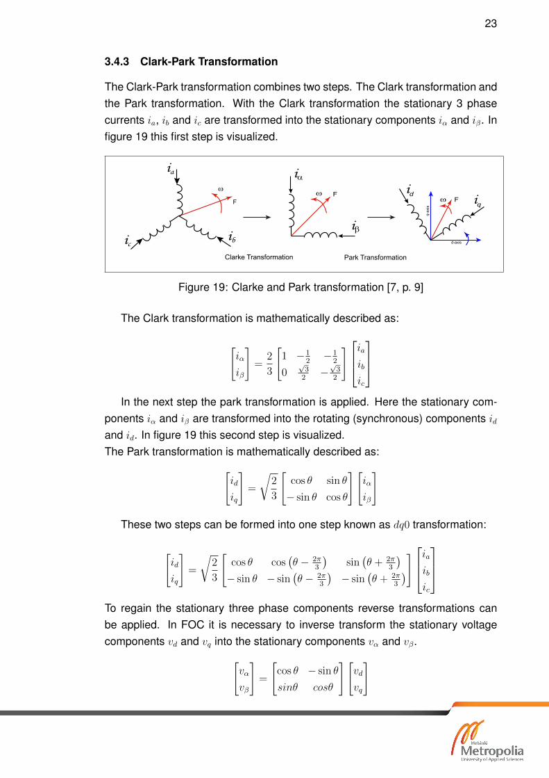
3.4.3 Clark-Park Transformation
The Clark-Park transformation combines two steps. The Clark transformation andthe Park transformation. With the Clark transformation the stationary 3 phasecurrents ia, ib and ic are transformed into the stationary components iα and iβ. Infigure 19 this first step is visualized.
Permanent Magnet Synchronous Motor
10 Revis ion 0
TransformationsIn FOC, the components Iq and Id are referenced to the rotating reference frame. Hence the measured stator currents have to be transformed from the three phase time variant stator reference frame to the two axis rotating dq rotor reference frame. This can be done in two steps as shown in Figure 1-5.
The transformation from the 3-phase 120 degree reference frame to two axis orthogonal reference frame is known as Clarke transform. Similarly the transformation from two axis orthogonal reference frame to the two axis rotating reference frame is known as Park transform.
Clarke TransformationThe measured motor currents are first translated from the 3-phase reference frame to the two axis orthogonal reference frame. The transform is expressed by the following equations.
Iα = Ia
Iβ = (Ia + 2Ib)/√3
Where Ia+Ib+Ic = 0
Park TransformationThe two axis orthogonal stationary reference frame quantities are then transformed to rotating reference frame quantities. The transform is expressed by the following equations:
Id = Iα cosθ + Iβ sinθ
Iq = Iβ cosθ – Iα sinθ
Inverse Park TransformationNow the outputs of the PI controllers provide the voltage components in the rotating reference frame. Thus an inverse of the previous process has to be applied to get the reference voltage waveforms in stationary reference frame. At first, the quantities in rotating reference frame are transformed to two axis orthogonal stationary reference frame using Inverse Park transformation. The Inverse Park transformation is expressed by the following equations:
Vα = Vd cosθ - Vq sinθ
Vβ = Vq cosθ + Vd sinθ
Figure 1-5 • Forward Transformations
ia
ibic
F
Clarke Transformation Park Transformation
i
i
F id iq
q-a
xis
d-axis
F
Figure 19: Clarke and Park transformation [7, p. 9]
The Clark transformation is mathematically described as:
[iα
iβ
]=
2
3
[1 −1
2−1
2
0√32−√32
]iaibic
In the next step the park transformation is applied. Here the stationary com-
ponents iα and iβ are transformed into the rotating (synchronous) components idand id. In figure 19 this second step is visualized.The Park transformation is mathematically described as:[
id
iq
]=
√2
3
[cos θ sin θ
− sin θ cos θ
][iα
iβ
]
These two steps can be formed into one step known as dq0 transformation:
[id
iq
]=
√2
3
[cos θ cos
(θ − 2π
3
)sin(θ + 2π
3
)− sin θ − sin
(θ − 2π
3
)− sin
(θ + 2π
3
)]iaibic
To regain the stationary three phase components reverse transformations canbe applied. In FOC it is necessary to inverse transform the stationary voltagecomponents vd and vq into the stationary components vα and vβ.[
vα
vβ
]=
[cos θ − sin θ
sinθ cosθ
][vd
vq
]

24
3.5 Switching Devices
3.5.1 MOSFET
Mosfet stands for metal-oxide-semiconductor field-effect transistor. The mosfetnowadays has replaced the bipolar transistor in low power switching applicationsalmost completely. Being a voltage controlled device it is more efficient and faster.
of device structure, geometry, and bias voltages. During turn-
on, capacitors Cgd and Cgs must be charged through the gate,
hence, the design of the gate control circuit must take into
consideration the variation in these capacitances. The largest
variation occurs in the gate-to-drain capacitance as the drain-
to-gate voltage varies. The MOSFET parasitic capacitance is
given in terms of the device data sheet parameters Ciss, Coss,
and Crss as follows:
Cgd ¼ Crss
Cgs ¼ Ciss ÿ Crss
Cds ¼ Coss ÿ Crss
where Crss is the small-signal reverse transfer capacitance; Ciss
is the small-signal input capacitance with the drain and source
terminals shorted; and Coss is the small-signal output capaci-
tance with the gate and source terminals shorted.
The MOSFET capacitances Cgs, Cgd and Cds are nonlinear
and a function of the dc bias voltage. The variations in Coss
and Ciss are significant as the drain-to-source voltage and the
gate-to-source voltage each cross zero. The objective of the
drive circuit is to charge and discharge the gate-to-source and
gate-to-drain parasitic capacitances to turn on and off the
device, respectively.
In power electronics, the aim is to use power-switching
devices that operate at higher and higher frequencies. Hence,
the size and weight of output transformers, inductors, and
filter capacitors will decrease. As a result, MOSFETs are now
used extensively in power supply design that requires high
switching frequencies, including switching and resonant mode
power supplies and brushless dc motor drives. Because of its
large conduction losses, its power rating is limited to a few
kilowatts. Because of its many advantages over BJT devices,
modern MOSFET devices have received high market accep-
tance.
6.6 MOSFET Regions of Operation
Most MOSFET devices used in power electronics applications
are of the n-channel, enhancement type, like that shown in
Fig. 6.6a. For the MOSFET to carry drain current, a channel
between the drain and the source must be created. This occurs
when the gate-to-source voltage exceeds the device threshold
voltage VTh. For vGS > VTh, the device can be either in the
triode region, which is also called ‘‘constant resistance’’ region,
or in the saturation region, depending on the value of vDS. For
given vGS, with small vDS (vDS < vGS ÿ VTh), the device oper-
ates in the triode region (saturation region in the BJT), and for
larger vDS ðvDS > vGS ÿ VTh), the device enters the saturation
region (active region in the BJT). For vGS < VTh, the device
turns off, with drain current almost equal to zero. Under both
regions of operation, the gate current is almost zero. This is
why the MOSFET is known as a voltage-driven device and,
therefore, requires simple gate control circuit.
The characteristic curves in Fig. 6.6b show that there are
three distinct regions of operation labeled as triode region,
saturation region, and cut-off region. When used as a switch-
ing device, only triode and cut-off regions are used, whereas,
when it is used as an amplifier, the MOSFET must operate in
the saturation region, which corresponds to the active region
in the BJT.
The device operates in the cut-off region (off-state) when
vGS < vTh, resulting in no induced channel. In order to operate
the MOSFET in either the triode or saturation region, a
channel must first be induced. This can be accomplished by
applying gate-to-source voltage that exceeds vTh, that is,
vGS > VTh
Once the channel is induced, the MOSFET can operate in
either the triode region (when the channel is continuous with
no pinch-off, resulting in drain current proportional to the
channel resistance) or the saturation region (the channel
pinches off, resulting in constant ID). The gate-to-drain bias
voltage (vGD) determines whether the induced channel enters
pinch-off or not. This is subject to the following restriction.
Cds
Cgd
Cgs
(a)
FIGURE 6.9 (a) Equivalent MOSFET representation including junc-
tion capacitances; and (b) representation of this physical location.
n+
n-
n+
n+
p
G
D
S
SiO2
S
Cg
d
Cds
Cgs
(b)
6 The Power MOSFET 83
Figure 20: (a) Equivalent MOSFET representation including junction capaci-tances; and (b) representation of this physical location.[9, p. 83]
In figure 20 you can see the physical structure of a mosfet with the location ofthe capacitances (b) and an equivalent representation (a). The behaviour of thecapacitance charging and discharging is almost exactly the same as with an igbt.In the following section this is explained in more detail. To understand the similarbehaviour in can be assumed that the drain of a mosfet is the collector of an igbtand the source of a mosfet is the emitter of an igbt.
3.5.2 IGBT
Igbt stands for insulated-gate bipolar transistor. The igbt combines the advan-tages of a mosfet and a bipolar transistor. The gate of an igbt, like a mosfet, isvoltage driven and needs little to ideally zero gate current. Like a bipolar transistorit is capable of conducting high currents. In figure 21 the physical structure, theequivalent circuit and the capacitance model are shown.

25
characteristics, good switching speed and excellent safe oper-
ating area. Compared to power MOSFETs the absence of the
integral body diode can be considered as an advantage or
disadvantage depending on the switching speed and current
requirements. An external fast-recovery diode or a diode in the
same package can be used for specific applications. The IGBTs
are replacing MOSFETs in high-voltage applications with
lower conduction losses. They have on-state voltage and
current density comparable to a power BJT with higher
switching frequency. Although they exhibit fast turn-on,
their turn-off is slower than a MOSFET because of current
fall time. Also, IGBTs have considerably less silicon area than
similar rated power MOSFETs. Therefore, by replacing power
MOSFETs with IGBTs, the efficiency is improved and cost is
reduced. Additionally, IGBT is known as a conductivity-
modulated FET (COMFET), insulated gate transistor (IGT),
and bipolar-mode MOSFET.
As soft-switching topologies offer numerous advantages
over the hard-switching topologies, their use is increasing in
the industry. By use of soft-switching techniques IGBTs can
operate at frequencies up to hundreds of kilohertz. However,
IGBTs behave differently under soft-switching condition
compared to their behavior under hard-switching conditions.
Therefore, the device trade-offs involved in soft-switching
circuits are different than those in the hard-switching case.
Application of IGBTs in high-power converters subjects them
to high-transient electrical stress such as short-circuit and
turn-off under clamped inductive load, and therefore robust-
ness of IGBTs under stress conditions is an important require-
ment. Traditionally, there has been limited interaction between
device manufacturers and power electronic circuit designers.
Therefore, the shortcomings of device reliability are observed
only after the devices are used in actual circuits. This signifi-
cantly slows down the process of power electronic system
optimization. However, the development time can be signifi-
cantly reduced if all issues of device performance and relia-
bility are taken into consideration at the design stage. As high
stress conditions are quite frequent in circuit applications, it is
extremely cost efficient and pertinent to model the IGBT
performance under these conditions. However, development
of the model can follow only after the physics of device
operation under stress conditions imposed by the circuit is
properly understood. Physically based process and device
simulations are a quick and cheap way of optimizing the
IGBT. The emergence of mixed-mode circuit simulators in
which semiconductor carrier dynamics is optimized within the
constraints of circuit level switching is a key design tool for
this task.
7.2 Basic Structure and Operation
The vertical cross section of a half cell of one of the parallel
cells of an n-channel IGBT shown in Fig. 7.2 is similar to that
of a double-diffused power MOSFET (DMOS) except for a
pþ-layer at the bottom. This layer forms the IGBT collector
and a pn-junction with nÿ-drift region, where conductivity
modulation occurs by injecting minority carriers into the
drain drift region of the vertical MOSFET. Therefore, the
current density is much greater than a power MOSFET and
the forward voltage drop is reduced. The pþ-substrate, nÿ-
drift layer and pþ-emitter constitute a BJT with a wide base
region and hence small current gain. The device operation can
be explained by a BJT with its base current controlled by the
voltage applied to the MOS gate. For simplicity, it is assumed
that the emitter terminal is connected to the ground potential.
By applying a negative voltage to the collector, the pn-junction
between the pþ-substrate and the nÿ-drift region is reverse-
biased, which prevents any current flow and the device is in its
reverse blocking state. If the gate terminal is kept at ground
potential but a positive potential is applied to the collector, the
pn-junction between the p-base and nÿ-drift region is reverse-
biased. This prevents any current flow and the device is in its
FIGURE 7.1 Hybrid Darlington configuration of MOSFET and BJT.
(a) (b)
FIGURE 7.2 The IGBT (a) half-cell vertical cross section and (b)
equivalent circuit model.
102 S. Abedinpour and K. Shenai
(a)
Application Note
Revision:
Issue Date:
Prepared by:
00
2007-10-31
Markus Hermwille
Key Words: IGBT driver, calculation, gate charge, power, gate current
IGBT Driver Calculation
AN-7004
1 / 8 2007-10-31 – Rev00 © by SEMIKRON
Introduction.............................................................................................................................................................................1 Gate Charge Curve ................................................................................................................................................................1 Measuring the Gate Charge ...................................................................................................................................................3 Determining the Gate Charge.................................................................................................................................................3 Driver Output Power...............................................................................................................................................................5 Gate Current...........................................................................................................................................................................5 Peak Gate Current..................................................................................................................................................................6 Selection Suitable IGBT Driver...............................................................................................................................................6 DriverSel – The Easy IGBT Driver Calculation Method ..........................................................................................................6 Symbols and Terms used.......................................................................................................................................................7 References .............................................................................................................................................................................8 This application note provides information on the determination of driver output performance for switching IGBTs. The information given in this application note contains tips only and does not constitute complete design rules; the information is not exhaustive. The responsibility for proper design remains with the user. Introduction One key component of every power electronic system is – besides the power modules themselves – the IGBT driver, which forms the vital interface between the power transistor and the controller. For this reason, the choice of driver and thus the calculation of the right driver output power are closely linked with the degree of reliability of a converter solution. Insufficient driver power or the wrong choice of driver may result in module and driver malfunction. Gate Charge Curve The switching behaviour (turn-on and turn-off) of an IGBT module is determined by its structural, internal capacitances (charges) and the internal and outer
resistances. When calculating the output power requirements for an IGBT driver circuit, the key parameter is the gate charge. This gate charge is characterised by the equivalent input capacitances CGC and CGE.
IGBT Capacitances
The following table explains the designation of the capacitances. In IGBT data sheets these capacitances are specified as voltage-dependent low-signal capacitances of IGBTs in the “off” state. The capacitances are independent of temperature, but dependent on the collector-emitter voltage, as shown in the following curve. This dependency is substantially higher at a very low collector-emitter voltage.
www.Semikron.com/Application/DriverCalculation
(b)
Figure 21: The IGBT (a) half-cell vertical cross section and equivalent circuitmodel[9, p. 102], (b) IGBT capacitances
Take a look at the igbt equivalent circuit in figure 21 (a). The igbt works as ifa bipolar npn transistor’s gate was driven by a mosfet’s gate. This npn transistorbecomes conductive and drives the gate of the high power pnp transistor.To switch an igbt efficiently the gate mosfet needs to be driven into saturationas quickly as possible. Therefore the capacitances seen in figure 21 (b) haveto be charged. In figure 22 (a) the sequence of charging the capacitances isshown. At first the gate-emitter capacitor is charged. When the gate-emittervoltage VGE(th) is reached, the igbt begins to conduct. When VGE(pl) is reached thegate-collector capacitance is charged in parallel. After crossing the Miller plateauthe gate-emitter capacitance becomes fully charged an VGE(on) is reached. Thegate charge of an igbt plays an important role in selecting and calculating a driver.The information about the gate charge can be found in the datasheet of the igbtmanufacturer. In 22 (b) an example gate charge curve can be seen. Dependingon the voltage applied to the collector and emitter and the ambient temperature,the capacitance varies.

26
Application Note AN-7004
2 / 8 2007-10-31 – Rev00 © by SEMIKRON
Parasitic and Low-Signal Capacitances Cies, Coes, Cres = f(VCE)
Capacitances Designation
CGE Gate-emitter capacitance
CCE Collector-emitter capacitance
CGC Gate-collector capacitance (Miller capacitance)
Low-Signal Capacitances Designation
Cies = CGE + CGC Input capacitance
Cres = CGC Reverse transfer capacitance
Coes = CGC + CCE Output capacitance
VGE = 0V f = 1MHz
The following table shows simplified the gate charge waveforms VGE= f(t), IG=f(t), VCE=f(t), and IC=f(t) during turn-on of the IGBT. The turn-on process can be divided into three stages. These are charging of the gate-emitter capacitance, charging of the gate-collector capacitance and charging of the gate-emitter capacitance until full IGBT saturation. To calculate the switching behaviour and the driver, the input capacitances may only be applied to a certain
extent. A more practical way of determining the driver output power is to use the gate charge characteristic given in the IGBT data sheets. This characteristic shows the gate-emitter voltage VGE over the gate charge QG. The gate charge increases in line with the current rating of IGBT modules. The gate charge is also dependent on the DC-Link voltage, albeit to a lesser extent. At higher operation voltages the gate charge increases due to the larger influence of the Miller capacitance. In most applications this effect is negligible.
Simplified Gate Charge Waveforms Gate Charge Characteristic
QGE QGC QGE
VGE(on)
VGE(off)
t0 switching interval: The gate current IG charges the input capacitance CGE and the gate-emitter voltage VGE rises to
VGE(th). Depending on the gate resistor, several amperes may be running in this state. As VGE is still below VGE(th), no collector current flows during this period and VCE is maintained at VCC level.
(a)
Application Note AN-7004
2 / 8 2007-10-31 – Rev00 © by SEMIKRON
Parasitic and Low-Signal Capacitances Cies, Coes, Cres = f(VCE)
Capacitances Designation
CGE Gate-emitter capacitance
CCE Collector-emitter capacitance
CGC Gate-collector capacitance (Miller capacitance)
Low-Signal Capacitances Designation
Cies = CGE + CGC Input capacitance
Cres = CGC Reverse transfer capacitance
Coes = CGC + CCE Output capacitance
VGE = 0V f = 1MHz
The following table shows simplified the gate charge waveforms VGE= f(t), IG=f(t), VCE=f(t), and IC=f(t) during turn-on of the IGBT. The turn-on process can be divided into three stages. These are charging of the gate-emitter capacitance, charging of the gate-collector capacitance and charging of the gate-emitter capacitance until full IGBT saturation. To calculate the switching behaviour and the driver, the input capacitances may only be applied to a certain
extent. A more practical way of determining the driver output power is to use the gate charge characteristic given in the IGBT data sheets. This characteristic shows the gate-emitter voltage VGE over the gate charge QG. The gate charge increases in line with the current rating of IGBT modules. The gate charge is also dependent on the DC-Link voltage, albeit to a lesser extent. At higher operation voltages the gate charge increases due to the larger influence of the Miller capacitance. In most applications this effect is negligible.
Simplified Gate Charge Waveforms Gate Charge Characteristic
QGE QGC QGE
VGE(on)
VGE(off)
t0 switching interval: The gate current IG charges the input capacitance CGE and the gate-emitter voltage VGE rises to
VGE(th). Depending on the gate resistor, several amperes may be running in this state. As VGE is still below VGE(th), no collector current flows during this period and VCE is maintained at VCC level.
(b)
Figure 22: (a) Simplified gate charge waveforms, (b) Gate charge characteristic[5, p. 2]

27
4 Matlab Simulation
powergui
ContinuousIdeal Switch
abc to dq transformation
iaibic
theta_e
id
iq fcn
Voltage Measurement2
v+-
Voltage Measurement1
v+-
Voltage Measurement
v+-
Vdc
Space Vector Generator and Gate Drive
vd_e
vq_e
ramptime
theta_e
Ts
Vdc
S1S2S3S4S5S6
sectort1
fcn
Scope5
Scope4
Scope3
Scope2
Scope1
Scope
RepeatingSequence
Product1
Product
Permanent MagnetSynchronous Machine
m
A
B
C
? ? ?
IGBT/S6/Sb'
g CE
IGBT/S5/Sc
g CE
IGBT/S4/Sa'
g CE
IGBT/S3/Sb
g CE
IGBT/S2/Sc'
g CE
IGBT/S1/Sa
g CE
Gain9
P/2
Gain3
60/(2*pi)
Gain2
psim
Gain1
P/2
DiscretePI Controller1
PI
DiscretePI Controller
PI
Current Measurement1
i+-
Current Measurement
i+-
Constant6
Ts
Constant5
Vdc
Constant4
0
Constant3
Ld
Constant2
Lq
Constant1
i_Sqref
Constant
i_Sdref
desired id_e
desired iq_e
S6S6S5
S5
S4S4
S3S3
S2S2
S1
S1
current ia
current ib
current ib
id_e_synchronousiq_e_synchronous
current ic
vd_e_synchronous
vq_e_synchronous
ramptime
ramptime
ramptime
<Rotor angle thetam (rad)>
<Rotor angle thetam (rad)>
<Rotor speed wm (rad/s)>
Rotor speed (rpm)
Figure 23: Matlab simulation of space vector pwm
As seen in figure 23 a Matlab simulation has been created to simulate thedynamic behaviour of a PMSM. Until now the results from the situation are notas expected. The simulation needs to be studied in more detail to see where theproblem is. The code for the space vector PWM and Clark-Park transformationcan be found in appendix A.4.
28
5 Schematic
5.1 Power Supply Module
<Drawn By>
<Checked By>
<QC By>
<Released By>
<Drawn Date>
<Checked Date>
<QC Date>
<Release Date>
<Company Name>
<Title>
<Code>
B
<Drawing Number>
<Revision>
<Scale>
1
1
REV:
SIZE:
CODE:
DRAWN:
DATED:
DATED:
CHECKED:
QUALITY CONTROL:
DATED:
DATED:
RELEASED:
COMPANY:
TITLE:
DRAWING NO:
SHEET: OF
SCALE:
REVISION RECORD
APPROVED:
ECO NO:
A
B
D
DATE:
1
2
3
4
5
6
D
C
A
B
C
LTR
Voltage Supplies
D-SUB Connector Power
1
IN
2
GND
3
OUT
U1
LM7805
C1
330nF
C2
100nF
J1-1
J1-2
J1-3
J1-4
J1-5
J1-6
J1-7
J1-8
J1-9
+
C34
100µF
+
C35
10µF
1
IN
2
GND
3
OUT
U6
LM7805
C13
330nF
C14
100nF
J2-1
J2-2
J2-3
J2-4
J2-5
J2-6
J2-7
J2-8
J2-9
J2-10
J3-1
J3-2
J3-3
J3-4
J3-5
J3-6
J3-7
J3-8
J3-9
J3-10
J2-11
J2-12
J2-13
J2-14
J2-15
J2-16
J2-17
J2-18
J2-19
J2-20
J3-11
J3-12
J3-13
J3-14
J3-15
J3-16
J3-17
J3-18
J3-19
J3-20
D17
F1
1
2
HEAT1
HEATSINK
1
-IN
2
+IN
4
-OUT
3
+OUT
DCDC1
AEE03A18-L
+12V
+12V
+12V
+12V
+12V
+5V
+12V_ISOLATED
GND_ISOLATED
+12V_ISOLATED
+5V_ISOLATED
+5V_ISOLATED
+5V
Figure 24: Power supply schematic
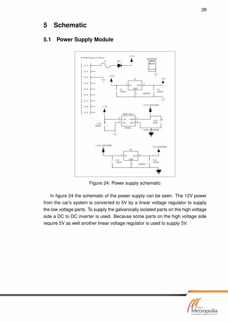
In figure 24 the schematic of the power supply can be seen. The 12V powerfrom the car’s system is converted to 5V by a linear voltage regulator to supplythe low voltage parts. To supply the galvanically isolated parts on the high voltageside a DC to DC inverter is used. Because some parts on the high voltage siderequire 5V as well another linear voltage regulator is used to supply 5V.

29
5.2 Microcontroller Modules
<Drawn By>
<Checked By>
<QC By>
<Released By>
<Drawn Date>
<Checked Date>
<QC Date>
<Release Date>
<Company Name>
<Title>
<Code>
A1
<Drawing Number>
<Revision>
<Scale>
1
1
REV:
SIZE:
CODE:
DRAWN:
DATED:
DATED:
CHECKED:
QUALITY CONTROL:
DATED:
DATED:
RELEASED:
COMPANY:
TITLE:
DRAWING NO:
SHEET: OF
SCALE:
REVISION RECORD
A
B
C
D
DATE:
1
2
3
4
5
6
D
C
B
A
LTR
ECO NO:
APPROVED:
Teensy2++
C2000 Launchpad
CAN Connector
JTAG Connector
1
GND
2
PB7/PCINT7/OC.0A/OC.1C
3
PD0/OC0B/SCL/INT0
4
PD1/OC2B/SDA/INT1
5
PD2/RXD1/INT2
6
PD3/TXD1/INT3
7
PD4/ICP1
8
PD5/XCK1
9
PD6/T1
10
PD7/T0
11
PE0/WR
12
PE1/RD
13
PC0/A8
14
PC1/A9
15
PC2/A10
16
PC3/A11/T.3
17
PC4/A12/OC.3C
18
PC5/A13/OC.3B
19
PC6/A14/OC.3A
20
PC7/A15/IC.3/CLKO
21
VCC
22
PB6/PCINT6/OC.1B
23
PB5/PCINT5/OC.1A
24
PB4/PCINT4/OC.2A
25
PB3/PDO/PCINT3/MISO
26
PB2/PDI/PCINT2/MOSI
27
PB1/PCINT1/SCLK
28
PB0/SS/PCINT0
29
PE7/INT.7/AIN.1/UVCON
30
PE6/INT.6/AIN.0
31
GND
32
AREF
33
PF0/ADC0
34
PF1/ADC1
35
PF2/ADC2
36
PF3/ADC3
37
PF4/ADC4/TCK
38
PF5/ADC5/TMS
39
PF6/ADC6/TDO
40
PF7/ADC7/TDI
41
+5V
42
GN
D
43
RST
B18
TEENSY++2.0
J1-1
+3.3V
J1-2
ADCINA6
J1-3
GPIO28/SCIRXDA/SDAA/TZ2
J1-4
GPIO29/SCITXDA/SCLA/TZ3
J1-5
GPIO34/COMP2OUT/RSVD/RSVD
J1-6
ADCINA4
J1-7
GPIO18/SPICLK/SCITXDA
J1-8
ADCINA2
J1-9
ADCINB2
J1-10
ADCINB4
J2-1
GND
J2-2
GPIO19/SPISTEA/SCIRXDA/ECAP1
J2-3
GPIO12/TZ1/SCITXDA/RSVD
J2-4
NC
J2-5
RESET
J2-6
GPIO16^32/SPISIMOA^SDAA/RSVD^EPWMSYNCI
J2-7
GPIO17^33/SPISOMIA^SCLA/RSVD^EPWMSYNCO
J2-8
GPIO6/EPWM4A/EPWMSYNCI/EPWMSYNCO
J2-9
GPIO7/EPWM4B/SCIRXDA/RSVD
J2-10
ADCINB6
J6-1
0
NC
J6-9
NC
J6-8
GPIO
17^
33/S
PIS
OM
IA^
SCLA/R
SVD
^EPW
MSYN
CO
J6-7
GPIO
16^
32/S
PIS
IMO
A^
SD
AA/R
SVD
^EPW
MSYN
CI
J6-6
GPIO
5/E
PW
M3B/R
SVD
/ECAP1
J6-5
GPIO
4/E
PW
M3A/R
SVD
/RSVD
J6-4
GPIO
3/E
PW
M2B/R
SVD
/CO
MP2O
UT
J6-3
GPIO
2/E
PW
M2A/R
SVD
/RSVD
J6-2
GPIO
1/E
PW
M1B/R
SVD
/CO
MP1O
UT
J6-1
GPIO
0/E
PW
M1A/R
SVD
/RSVD
J5-1
0
NC
J5-9
AD
CIN
B7
J5-8
AD
CIN
B3
J5-7
AD
CIN
B1
J5-6
AD
CIN
A0
J5-5
AD
CIN
A1
J5-4
AD
CIN
A3
J5-3
AD
CIN
A7
J5-2
GN
D
J5-1
+5V
J3-1
GND
J3-2
GND
J3-3
+3.3V
B1
C2000LAUNCHPAD
1
GND
2
CANL
3
GND
4
NC
5
NC
6
NC
7
CANH
8
NC
9
NC
10
GND
20
VCC
19
SPI_CS_TEENSY
18
SPI_MISO_TEENSY
17
SPI_MOSI_TEENSY
16
SPI_CLK_TEENSY
15
SPI_INT_TEENSY
14
NC
13
GND
12
GND
11
GND
CANMODULE1
CANMODULE
1
VSS
2
VDD
3
V0
4
RS
5
R/W
6
EN
7
DB0
8
DB1
9
DB2
10
DB3
11
DB4
12
DB5
13
DB6
14
DB7
LCD
1
GTC-1
6026
1
+5V
2
NC
3
NC
4
TEMP_OS
5
SCL
6
SDA
7
NC
8
GND
9
GND
10
GND
20
+5V2
19
GND2
18
NC
17
SDA2
16
SCL2
15
TEMP_OS2
14
NC
13
GND2
12
GND2
11
GND2
OPTO1
OPTOCOUPLERMODULE
J1-1
J1-2
J1-3
J1-4
J1-5
J1-6
J1-7
J1-8
J1-9
1
+12V
2
NC
9
NC
10
GND
11
NC
17
SPI_MISO_C2000
18
SPI_MOSI_C2000
19
SPI_CLK_C2000
20
GND
40
+12V
39
GND
34
R2D_A0
33
R2D_A1
32
R2D_LOT
31
R2D_RESET
30
R2D_WR/FSYNC
29
R2D_SAMPLE
22
NC
21
NC
R2D1
RESOLVER2DIGITALMODULE
J2-1
J2-2
J2-3
J2-4
J2-5
J2-6
J2-7
J2-8
J2-9
J2-10
1
+12V
2
+12V
3
+12V
4
NC
5
NC
6
NC
7
NC
8
NC
9
GND
10
GND
11
GND
12
NC
13
NC
14
NC
15
NC
16
NC
17
NC
18
+5V
19
+5V
20
+5V
40
+12V
39
+12V
38
+12V
37
NC
36
NC
31
+12V_ISOLATED
30
+12V_ISOLATED
29
+12V_ISOLATED
28
NC
27
GND_ISOLATED
26
GND_ISOLATED
25
GND_ISOLATED
24
NC
23
+5V_ISOLATED
22
+5V_ISOLATED
21
+5V_ISOLATED
POWER1
POWERSUPPLYMODULE
1
GND
2
NC
3
NC
4
NC
5
EPWM3A
6
+5V
7
EPWM2B
8
EPWM2A
9
EPWM1B
10
EPWM1A
11
EPWM3B
12
CURRENT_SENS1_OUT
13
CURRENT_SENS2_OUT
14
OVERCURRENT1_FAULT
15
OVERCURRENT2_FAULT
16
OVERCURRENT3_FAULT
17
+5V
18
NC
19
NC
20
GND
21
NC
22
PC7_TEENSY
23
PC6_TEENSY
24
PC5_TEENSY
25
PC4_TEENSY
26
PC3_TEENSY
27
PC2_TEENSY
28
PC1_TEENSY
29
PC0_TEENSY
30
PE0_TEENSY
31
PE1_TEENSY
32
OVER_CURRENT_FAULT_RESET
33
NC
34
NC
35
SDA_ISOLATED
36
SCL_ISOLATED
37
TEMP_OS_ISOLATED
38
NC
39
NC
40
NC
51
NC
52
NC
53
EPWM2A
54
EPWM1A
55
+5V
56
NC
57
NC
58
GND
59
CURRENT_SENS1_OUT
60
+5V
119
GND_ISOLATED
118
NC
117
NC
116
NC
115
NC
114
NC
113
NC
112
NC
111
NC
110
+5V_ISOLATED
109
NC
108
+12V_ISOLATED
107
NC
106
NC
105
NC
104
NC
103
NC
102
NC
101
NC
100
NC
99
NC
98
NC
97
NC
96
NC
95
NC
94
NC
93
NC
92
NC
91
NC
90
NC
120
NC
89
NC
88
NC
87
NC
86
NC
85
NC
84
NC
83
NC
82
NC
81
NC
80
NC
79
NC
78
NC
77
NC
76
NC
75
NC
74
NC
73
NC
72
SDA_ISOLATED
71
SCL_ISOLATED
70
TEMP_OS_ISOLATED
69
NC
68
EPWM3A
67
NC
66
CURRENT_SENS3_OUT
65
NC
64
NC
63
NC
62
NC
61
NC
INV1
INVERTERMODULEMOSFET
1
2
R1
120R
1
2
R2
1k2R
D1
C1
10nF
1
2
R3
120R
1
2
R4
1k2R
D2
C2
10nF
1
2
R5
120R
1
2
R6
1k2R
D3
C3
10nF
1
2
R7
120R
1
2
R8
1k2R
D4
C4
10nF
1
2
R9
120R
1
2
R10
1k2R
D5
C5
10nF
1
2
R11
120R
1
2
R12
1k2R
D6
C6
10nF
1
2
R13
120R
1
2
R14
1k2R
D7
C7
10nF
1
2
R15
120R
1
2
R16
1k2R
D8
C8
10nF
1
2
R17
120R
1
2
R18
1k2R
D9
C9
10nF
1
2
R19
120R
1
2
R20
1k2R
D10
C10
10nF
1
2
R21
120R
1
2
R22
1k2R
D11
C11
10nF
1
2
R23
120R
1
2
R24
1k2R
D12
C12
10nF
1
2
R25
120R
1
2
R26
1k2R
D13
C13
10nF
1
2
R27
120R
1
2
R28
1k2R
D14
C14
10nF
1
2
R29
120R
1
2
R30
1k2R
D15
C15
10nF
1
2
R31
120R
1
2
R32
1k2R
D16
C16
10nF
1
2
R33
120R
1
2
R34
1k2R
D17
C17
10nF
1
2
R35
120R
1
2
R36
1k2R
D18
C18
10nF
1
2
R37
120R
1
2
R38
1k2R
D19
C19
10nF
1
2
R39
120R
1
2
R40
1k2R
D20
C20
10nF
1
2
R43
120R
1
2
R44
1k2R
D22
C22
10nF
1
2
R45
120R
1
2
R46
1k2R
D23
C23
10nF
1
2
R41
120R
1
2
R42
1k2R
D21
C21
10nF
1
2
R47
120R
1
2
R48
1k2R
D24
C24
10nF
1
2
R49
120R
1
2
R50
1k2R
D25
C25
10nF
1
2
R51
120R
1
2
R52
1k2R
D26
C26
10nF
1
2
R54
1k2R
1
2
R69
120R
1
2
R71
120R
1
2
R73
120R
1
2
R75
120R
1
2
R77
120R
1
2
R79
120R
FET1
FET2
1
2
R55
120R
1
2
R56
1k2R
D28
1
2
R57
120R
1
2
R59
120R
1
2
R60
1k2R
D30
C29
10nF
C30
10nF
1
2
R61
120R
1
2
R62
1k2R
D32
C31
10nF
1
2
R63
120R
1
2
R64
1k2R
D33
C32
10nF
1
2
R65
120R
1
2
R66
1k2R
D31
C33
10nF
1
2
R67
120R
D40
C40
10nF
1
2
R81
120R
D41
C41
10nF
1
2
R83
1k2R
1
2
R84
1k2R
1
2
R85
47k
1
2
R86
47k
1
2
R87
120R
D42
1
2
R89
120R
1
2
R91
120R
1
2
R93
120R
1
2
R95
120R
1
2
R97
120R
1
2
R99
120R
1
2
R100
1k2R
D48
C48
10nF
1
2
R101
120R
1
2
R102
1k2R
D49
C49
10nF
1
2
R103
120R
1
2
R104
1k2R
D50
C50
10nF
1
2
R105
120R
1
2
R106
1k2R
D51
C51
10nF
1
2
R107
120R
1
2
R108
1k2R
D52
C52
10nF
1
2
R109
120R
1
2
R110
1k2R
D53
C53
10nF
1
2
R111
120R
1
2
R112
1k2R
D54
C54
10nF
1
2
R113
120R
1
2
R114
1k2R
D55
C55
10nF
1
2
R115
120R
1
2
R117
120R
1
2
R130
120R
1
2
R131
1k2R
D69
C58
10nF
D43
D44
D45
D46
D34
D35
D36
D37
D38
D39
D47
D56
D29
1
2
R58
120R
D57
1
2
R70
1k2R
1
2
R72
1k2R
C34
10nF
C35
10nF
C36
10nF
C37
10nF
C38
10nF
C39
10nF
C42
10nF
C43
10nF
1
2
R92
1k2R
1
2
R94
1k2R
1
2
R96
1k2R
1
2
R98
1k2R
1
2
R116
1k2R
1
2
R118
1k2R
D58
C44
10nF
C45
10nF
C46
10nF
C47
10nF
C56
10nF
C57
10nF
1
2
R119
1k2R
1
2
R120
1k2R
C59
10nF
C60
10nF
1
2
R53
1k2R
1
2
R121
1k2R
1
2
R122
1k2R
1
2
R123
120R
1
2
R124
120R
1
2
R125
120R
C27
10nF
C28
10nF
C61
10nF
D27
D59
D60
+12V
+12V
+12V
+12V
+5V
EPWM3A
EPWM2B
EPWM2A
EPWM1B
EPWM1A
EPWM3B
CURRENT_SENS1_OUT
PC7_TEENSY
PC6_TEENSY
PC5_TEENSY
PC4_TEENSY
PC3_TEENSY
PC2_TEENSY
PC1_TEENSY
PC0_TEENSY
PE0_TEENSY
PE1_TEENSY
OVER_CURRENT_FAULT_RESET
SDA_ISOLATED
SCL_ISOLATED
TEMP_OS_ISOLATED
EPWM2A
EPWM1A
CURRENT_SENS1_OUT
EPWM3A
TEMP_OS_ISOLATED
SCL_ISOLATED
SDA_ISOLATED
CANL
CANH
TEMP_OS_ISOLATED
SCL_ISOLATED
SDA_ISOLATED
SDA
SCL
TEMP_OS
CANL
CANH
PF4/TCK_TEENSY
PF6/TDO_TEENSY
PF5/TMS_TEENSY
JTAG_NSRST
PF7/TDI_TEENSY
+5V
PD6_LCD_RW
OVER_CURRENT_FAULT_RESET
PD5_LCD_EN
PD7_LCD_RS
PC0_TEENSY
PC1_TEENSY
PC2_TEENSY
PC3_TEENSY
PC4_TEENSY
PC5_TEENSY
PC6_TEENSY
PC7_TEENSY
PE1_TEENSY
PE0_TEENSY
PF6/TDO_TEENSY
PF5/TMS_TEENSY
PF4/TCK_TEENSY
PF7/TDI_TEENSY
PF3_TEENSY
PF2_TEENSY
PF1_TEENSY
PF0_TEENSY
SPI_CLK_TEENSY
SPI_MOSI_TEENSY
SPI_MISO_TEENSY
INT.7_TEENSY
JTAG_NSRST
EPW
M1A
EPW
M1B
EPW
M2A
EPW
M2B
EPW
M3A
EPW
M3B
TEMP_OS
OVERCURRENT1_FAULT
OVERCURRENT2_FAULT
OVERCURRENT3_FAULT
OVERCURRENT3_FAULT
OVERCURRENT2_FAULT
OVERCURRENT1_FAULT
SDA
SCL
SPI_MISO_C2000
SDA
SCL
+3.3V
SPI_MOSI_C2000
SPI_MISO_C2000
R2D_LOT
R2D_RESET
R2D_A0
R2D_A1
R2D_A0
R2D_A1
R2D_LOT
R2D_RESET
R2D_WR/FSYNC
R2D_SAMPLE
SPI_
MO
SI_
C2000
SPI_
CLK_C2000
R2D
_SAM
PLE
R2D
_W
R/F
SYN
C
PD5_LCD_EN
PD6_LCD_RW
PD7_LCD_RS
PF7/TDI_TEENSY
PF6/TDO_TEENSY
PF5/TMS_TEENSY
PF4/TCK_TEENSY
PF3_TEENSY
PF2_TEENSY
PF1_TEENSY
PF0_TEENSY
SPI_SS_TEENSY
INT.7_TEENSY
SPI_CLK_TEENSY
SPI_MOSI_TEENSY
SPI_MISO_TEENSY
SPI_SS_TEENSY
SPI_CLK_C2000
+3.3V
CURRENT_SENS3_OUT
CURRENT_SENS2_OUT
CURRENT_SENS1_OUT
CURRENT_SENS2_OUT
CURRENT_SENS3_OUT
Figure 25: Teensy2++ schematic
In figure 25 and 26 the schematic of the Teensy2++ and the C2000 launchpadcan be seen. The I/Os of the microcontrollers are protected by a zener diodeagainst voltage transients. Also a resistor directly at the input protects the interiordiodes of the microcontroller against too high currents.
<Drawn By>
<Checked By>
<QC By>
<Released By>
<Drawn Date>
<Checked Date>
<QC Date>
<Release Date>
<Company Name>
<Title>
<Code>
A1
<Drawing Number>
<Revision>
<Scale>
1
1
REV:
SIZE:
CODE:
DRAWN:
DATED:
DATED:
CHECKED:
QUALITY CONTROL:
DATED:
DATED:
RELEASED:
COMPANY:
TITLE:
DRAWING NO:
SHEET: OF
SCALE:
REVISION RECORD
A
B
C
D
DATE:
1
2
3
4
5
6
D
C
B
A
LTR
ECO NO:
APPROVED:
Teensy2++
C2000 Launchpad
CAN Connector
JTAG Connector
1
GND
2
PB7/PCINT7/OC.0A/OC.1C
3
PD0/OC0B/SCL/INT0
4
PD1/OC2B/SDA/INT1
5
PD2/RXD1/INT2
6
PD3/TXD1/INT3
7
PD4/ICP1
8
PD5/XCK1
9
PD6/T1
10
PD7/T0
11
PE0/WR
12
PE1/RD
13
PC0/A8
14
PC1/A9
15
PC2/A10
16
PC3/A11/T.3
17
PC4/A12/OC.3C
18
PC5/A13/OC.3B
19
PC6/A14/OC.3A
20
PC7/A15/IC.3/CLKO
21
VCC
22
PB6/PCINT6/OC.1B
23
PB5/PCINT5/OC.1A
24
PB4/PCINT4/OC.2A
25
PB3/PDO/PCINT3/MISO
26
PB2/PDI/PCINT2/MOSI
27
PB1/PCINT1/SCLK
28
PB0/SS/PCINT0
29
PE7/INT.7/AIN.1/UVCON
30
PE6/INT.6/AIN.0
31
GND
32
AREF
33
PF0/ADC0
34
PF1/ADC1
35
PF2/ADC2
36
PF3/ADC3
37
PF4/ADC4/TCK
38
PF5/ADC5/TMS
39
PF6/ADC6/TDO
40
PF7/ADC7/TDI
41
+5V
42
GND
43
RST
B18
TEENSY++2.0
J1-1
+3.3V
J1-2
ADCINA6
J1-3
GPIO28/SCIRXDA/SDAA/TZ2
J1-4
GPIO29/SCITXDA/SCLA/TZ3
J1-5
GPIO34/COMP2OUT/RSVD/RSVD
J1-6
ADCINA4
J1-7
GPIO18/SPICLK/SCITXDA
J1-8
ADCINA2
J1-9
ADCINB2
J1-10
ADCINB4
J2-1
GND
J2-2
GPIO19/SPISTEA/SCIRXDA/ECAP1
J2-3
GPIO12/TZ1/SCITXDA/RSVD
J2-4
NC
J2-5
RESET
J2-6
GPIO16^32/SPISIMOA^SDAA/RSVD^EPWMSYNCI
J2-7
GPIO17^33/SPISOMIA^SCLA/RSVD^EPWMSYNCO
J2-8
GPIO6/EPWM4A/EPWMSYNCI/EPWMSYNCO
J2-9
GPIO7/EPWM4B/SCIRXDA/RSVD
J2-10
ADCINB6
J6-1
0
NC
J6-9
NC
J6-8
GPIO
17^
33/S
PIS
OM
IA^
SCLA/R
SVD^
EPW
MSYNCO
J6-7
GPIO
16^
32/S
PIS
IMO
A^
SDAA/R
SVD^
EPW
MSYNCI
J6-6
GPIO
5/E
PW
M3B/R
SVD/E
CAP1
J6-5
GPIO
4/E
PW
M3A/R
SVD/R
SVD
J6-4
GPIO
3/E
PW
M2B/R
SVD/C
OM
P2O
UT
J6-3
GPIO
2/E
PW
M2A/R
SVD/R
SVD
J6-2
GPIO
1/E
PW
M1B/R
SVD/C
OM
P1O
UT
J6-1
GPIO
0/E
PW
M1A/R
SVD/R
SVD
J5-1
0
NC
J5-9
ADCIN
B7
J5-8
ADCIN
B3
J5-7
ADCIN
B1
J5-6
ADCIN
A0
J5-5
ADCIN
A1
J5-4
ADCIN
A3
J5-3
ADCIN
A7
J5-2
GND
J5-1
+5V
J3-1
GND
J3-2
GND
J3-3
+3.3V
B1
C2000LAUNCHPAD
1
GND
2
CANL
3
GND
4
NC
5
NC
6
NC
7
CANH
8
NC
9
NC
10
GND
20
VCC
19
SPI_CS_TEENSY
18
SPI_MISO_TEENSY
17
SPI_MOSI_TEENSY
16
SPI_CLK_TEENSY
15
SPI_INT_TEENSY
14
NC
13
GND
12
GND
11
GND
CANMODULE1
CANMODULE
1
VSS
2
VDD
3
V0
4
RS
5
R/W
6
EN
7
DB0
8
DB1
9
DB2
10
DB3
11
DB4
12
DB5
13
DB6
14
DB7
LCD1
GTC-1
6026
1
+5V
2
NC
3
NC
4
TEMP_OS
5
SCL
6
SDA
7
NC
8
GND
9
GND
10
GND
20
+5V2
19
GND2
18
NC
17
SDA2
16
SCL2
15
TEMP_OS2
14
NC
13
GND2
12
GND2
11
GND2
OPTO1
OPTOCOUPLERMODULE
J1-1
J1-2
J1-3
J1-4
J1-5
J1-6
J1-7
J1-8
J1-9
1
+12V
2
NC
9
NC
10
GND
11
NC
17
SPI_MISO_C2000
18
SPI_MOSI_C2000
19
SPI_CLK_C2000
20
GND
40
+12V
39
GND
34
R2D_A0
33
R2D_A1
32
R2D_LOT
31
R2D_RESET
30
R2D_WR/FSYNC
29
R2D_SAMPLE
22
NC
21
NC
R2D1
RESOLVER2DIGITALMODULE
J2-1
J2-2
J2-3
J2-4
J2-5
J2-6
J2-7
J2-8
J2-9
J2-10
1
+12V
2
+12V
3
+12V
4
NC
5
NC
6
NC
7
NC
8
NC
9
GND
10
GND
11
GND
12
NC
13
NC
14
NC
15
NC
16
NC
17
NC
18
+5V
19
+5V
20
+5V
40
+12V
39
+12V
38
+12V
37
NC
36
NC
31
+12V_ISOLATED
30
+12V_ISOLATED
29
+12V_ISOLATED
28
NC
27
GND_ISOLATED
26
GND_ISOLATED
25
GND_ISOLATED
24
NC
23
+5V_ISOLATED
22
+5V_ISOLATED
21
+5V_ISOLATED
POWER1
POWERSUPPLYMODULE
1
GND
2
NC
3
NC
4
NC
5
EPWM3A
6
+5V
7
EPWM2B
8
EPWM2A
9
EPWM1B
10
EPWM1A
11
EPWM3B
12
CURRENT_SENS1_OUT
13
CURRENT_SENS2_OUT
14
OVERCURRENT1_FAULT
15
OVERCURRENT2_FAULT
16
OVERCURRENT3_FAULT
17
+5V
18
NC
19
NC
20
GND
21
NC
22
PC7_TEENSY
23
PC6_TEENSY
24
PC5_TEENSY
25
PC4_TEENSY
26
PC3_TEENSY
27
PC2_TEENSY
28
PC1_TEENSY
29
PC0_TEENSY
30
PE0_TEENSY
31
PE1_TEENSY
32
OVER_CURRENT_FAULT_RESET
33
NC
34
NC
35
SDA_ISOLATED
36
SCL_ISOLATED
37
TEMP_OS_ISOLATED
38
NC
39
NC
40
NC
51
NC
52
NC
53
EPWM2A
54
EPWM1A
55
+5V
56
NC
57
NC
58
GND
59
CURRENT_SENS1_OUT
60
+5V
119
GND_ISOLATED
118
NC
117
NC
116
NC
115
NC
114
NC
113
NC
112
NC
111
NC
110
+5V_ISOLATED
109
NC
108
+12V_ISOLATED
107
NC
106
NC
105
NC
104
NC
103
NC
102
NC
101
NC
100
NC
99
NC
98
NC
97
NC
96
NC
95
NC
94
NC
93
NC
92
NC
91
NC
90
NC
120
NC
89
NC
88
NC
87
NC
86
NC
85
NC
84
NC
83
NC
82
NC
81
NC
80
NC
79
NC
78
NC
77
NC
76
NC
75
NC
74
NC
73
NC
72
SDA_ISOLATED
71
SCL_ISOLATED
70
TEMP_OS_ISOLATED
69
NC
68
EPWM3A
67
NC
66
CURRENT_SENS3_OUT
65
NC
64
NC
63
NC
62
NC
61
NC
INV1
INVERTERMODULEMOSFET
1
2
R1
120R
1
2
R2
1k2R
D1
C1
10nF
1
2
R3
120R
1
2
R4
1k2R
D2
C2
10nF
1
2
R5
120R
1
2
R6
1k2R
D3
C3
10nF
1
2
R7
120R
1
2
R8
1k2R
D4
C4
10nF
1
2
R9
120R
1
2
R10
1k2R
D5
C5
10nF
1
2
R11
120R
1
2
R12
1k2R
D6
C6
10nF
1
2
R13
120R
1
2
R14
1k2R
D7
C7
10nF
1
2
R15
120R
1
2
R16
1k2R
D8
C8
10nF
1
2
R17
120R
1
2
R18
1k2R
D9
C9
10nF
1
2
R19
120R
1
2
R20
1k2R
D10
C10
10nF
1
2
R21
120R
1
2
R22
1k2R
D11
C11
10nF
1
2
R23
120R
1
2
R24
1k2R
D12
C12
10nF
1
2
R25
120R
1
2
R26
1k2R
D13
C13
10nF
1
2
R27
120R
1
2
R28
1k2R
D14
C14
10nF
1
2
R29
120R
1
2
R30
1k2R
D15
C15
10nF
1
2
R31
120R
1
2
R32
1k2R
D16
C16
10nF
1
2
R33
120R
1
2
R34
1k2R
D17
C17
10nF
1
2
R35
120R
1
2
R36
1k2R
D18
C18
10nF
1
2
R37
120R
1
2
R38
1k2R
D19
C19
10nF
1
2
R39
120R
1
2
R40
1k2R
D20
C20
10nF
1
2
R43
120R
1
2
R44
1k2R
D22
C22
10nF
1
2
R45
120R
1
2
R46
1k2R
D23
C23
10nF
1
2
R41
120R
1
2
R42
1k2R
D21
C21
10nF
1
2
R47
120R
1
2
R48
1k2R
D24
C24
10nF
1
2
R49
120R
1
2
R50
1k2R
D25
C25
10nF
1
2
R51
120R
1
2
R52
1k2R
D26
C26
10nF
1
2
R54
1k2R
1
2
R69
120R
1
2
R71
120R
1
2
R73
120R
1
2
R75
120R
1
2
R77
120R
1
2
R79
120R
FET1
FET2
1
2
R55
120R
1
2
R56
1k2R
D28
1
2
R57
120R
1
2
R59
120R
1
2
R60
1k2R
D30
C29
10nF
C30
10nF
1
2
R61
120R
1
2
R62
1k2R
D32
C31
10nF
1
2
R63
120R
1
2
R64
1k2R
D33
C32
10nF
1
2
R65
120R
1
2
R66
1k2R
D31
C33
10nF
1
2
R67
120R
D40
C40
10nF
1
2
R81
120R
D41
C41
10nF
1
2
R83
1k2R
1
2
R84
1k2R
1
2
R85
47k
1
2
R86
47k
1
2
R87
120R
D42
1
2
R89
120R
1
2
R91
120R
1
2
R93
120R
1
2
R95
120R
1
2
R97
120R
1
2
R99
120R
1
2
R100
1k2R
D48
C48
10nF
1
2
R101
120R
1
2
R102
1k2R
D49
C49
10nF
1
2
R103
120R
1
2
R104
1k2R
D50
C50
10nF
1
2
R105
120R
1
2
R106
1k2R
D51
C51
10nF
1
2
R107
120R
1
2
R108
1k2R
D52
C52
10nF
1
2
R109
120R
1
2
R110
1k2R
D53
C53
10nF
1
2
R111
120R
1
2
R112
1k2R
D54
C54
10nF
1
2
R113
120R
1
2
R114
1k2R
D55
C55
10nF
1
2
R115
120R
1
2
R117
120R
1
2
R130
120R
1
2
R131
1k2R
D69
C58
10nF
D43
D44
D45
D46
D34
D35
D36
D37
D38
D39
D47
D56
D29
1
2
R58
120R
D57
1
2
R70
1k2R
1
2
R72
1k2R
C34
10nF
C35
10nF
C36
10nF
C37
10nF
C38
10nF
C39
10nF
C42
10nF
C43
10nF
1
2
R92
1k2R
1
2
R94
1k2R
1
2
R96
1k2R
1
2
R98
1k2R
1
2
R116
1k2R
1
2
R118
1k2R
D58
C44
10nF
C45
10nF
C46
10nF
C47
10nF
C56
10nF
C57
10nF
1
2
R119
1k2R
1
2
R120
1k2R
C59
10nF
C60
10nF
1
2
R53
1k2R
1
2
R121
1k2R
1
2
R122
1k2R
1
2
R123
120R
1
2
R124
120R
1
2
R125
120R
C27
10nF
C28
10nF
C61
10nF
D27
D59
D60
+12V
+12V
+12V
+12V
+5V
EPWM3A
EPWM2B
EPWM2A
EPWM1B
EPWM1A
EPWM3B
CURRENT_SENS1_OUT
PC7_TEENSY
PC6_TEENSY
PC5_TEENSY
PC4_TEENSY
PC3_TEENSY
PC2_TEENSY
PC1_TEENSY
PC0_TEENSY
PE0_TEENSY
PE1_TEENSY
OVER_CURRENT_FAULT_RESET
SDA_ISOLATED
SCL_ISOLATED
TEMP_OS_ISOLATED
EPWM2A
EPWM1A
CURRENT_SENS1_OUT
EPWM3A
TEMP_OS_ISOLATED
SCL_ISOLATED
SDA_ISOLATED
CANL
CANH
TEMP_OS_ISOLATED
SCL_ISOLATED
SDA_ISOLATED
SDA
SCL
TEMP_OS
CANL
CANH
PF4/TCK_TEENSY
PF6/TDO_TEENSY
PF5/TMS_TEENSY
JTAG_NSRST
PF7/TDI_TEENSY
+5V
PD6_LCD_RW
OVER_CURRENT_FAULT_RESET
PD5_LCD_EN
PD7_LCD_RS
PC0_TEENSY
PC1_TEENSY
PC2_TEENSY
PC3_TEENSY
PC4_TEENSY
PC5_TEENSY
PC6_TEENSY
PC7_TEENSY
PE1_TEENSY
PE0_TEENSY
PF6/TDO_TEENSY
PF5/TMS_TEENSY
PF4/TCK_TEENSY
PF7/TDI_TEENSY
PF3_TEENSY
PF2_TEENSY
PF1_TEENSY
PF0_TEENSY
SPI_CLK_TEENSY
SPI_MOSI_TEENSY
SPI_MISO_TEENSY
INT.7_TEENSY
JTAG_NSRST
EPW
M1A
EPW
M1B
EPW
M2A
EPW
M2B
EPW
M3A
EPW
M3B
TEMP_OS
OVERCURRENT1_FAULT
OVERCURRENT2_FAULT
OVERCURRENT3_FAULT
OVERCURRENT3_FAULT
OVERCURRENT2_FAULT
OVERCURRENT1_FAULT
SDA
SCL
SPI_MISO_C2000
SDA
SCL
+3.3V
SPI_MOSI_C2000
SPI_MISO_C2000
R2D_LOT
R2D_RESET
R2D_A0
R2D_A1
R2D_A0
R2D_A1
R2D_LOT
R2D_RESET
R2D_WR/FSYNC
R2D_SAMPLE
SPI_
MO
SI_
C2000
SPI_
CLK_C2000
R2D_SAM
PLE
R2D_W
R/F
SYNC
PD5_LCD_EN
PD6_LCD_RW
PD7_LCD_RS
PF7/TDI_TEENSY
PF6/TDO_TEENSY
PF5/TMS_TEENSY
PF4/TCK_TEENSY
PF3_TEENSY
PF2_TEENSY
PF1_TEENSY
PF0_TEENSY
SPI_SS_TEENSY
INT.7_TEENSY
SPI_CLK_TEENSY
SPI_MOSI_TEENSY
SPI_MISO_TEENSY
SPI_SS_TEENSY
SPI_CLK_C2000
+3.3V
CURRENT_SENS3_OUT
CURRENT_SENS2_OUT
CURRENT_SENS1_OUT
CURRENT_SENS2_OUT
CURRENT_SENS3_OUT
Figure 26: C2000 launchpad schematic

30
<Drawn By>
<Checked By>
<QC By>
<Released By>
<Drawn Date>
<Checked Date>
<QC Date>
<Release Date>
<Company Name>
<Title>
<Code>
B
<Drawing Number>
<Revision>
<Scale>
1
1
REV:
SIZE:
CODE:
DRAWN:
DATED:
DATED:
CHECKED:
QUALITY CONTROL:
DATED:
DATED:
RELEASED:
COMPANY:
TITLE:
DRAWING NO:
SHEET: OF
SCALE:
REVISION RECORD
APPROVED:
ECO NO:
A
B
D
DATE:
1
2
3
4
5
6
D
C
A
B
C
LTR
Optocoupler Isolation
1
SDA
7
SCL
3
TXD,SDA
2
RXD,SDA
5
TXD,SCL
6
RXD,SCL
8
VCC
4
GND
B11
P82B96
1
2
R22
¨1k5
1
2
R23
1k5
VF2
VF1
1
+
2
-
3
-
4
+
8
VCC
7
VO1
6
VO2
5
GND
B15
HCPL2630
1
2
R24
390
1
2
R25
390R
1
2
R26
390R
VF2
VF1
1
+
2
-
3
-
4
+
8
VCC
7
VO1
6
VO2
5
GND
B16
HCPL2630
1
2
R27
390
1
2
OC
U4-A
7417
1
2
R28
1k
3
4
OC
U4-B
7417
1
2
R34
390
J2-1
J2-2
J2-3
J2-4
J2-5
J2-6
J2-7
J2-8
J2-9
J2-10
J1-1
J1-2
J1-3
J1-4
J1-5
J1-6
J1-7
J1-8
J1-9
J1-10
1
2
R1
1k
SDA
SCL
SCL
SDA_ISOLATED
SCL_ISOLATED
+5V_ISOLATED
TEMP_OS_ISOLATED
TEMP_OS
+5V
SCL
+5V
SDA_ISOLATED
SCL_ISOLATED
TEMP_OS_ISOLATED
TEMP_OS
SDA
Figure 27: Optocoupler module schematic
5.3 Optocoupler Module
In figure 27 the optocoupler module can be seen. It uses the P82B96 IC (inte-grated circuit) and two fast optocouplers to galvanically isolate the high voltageside from the low voltage side of the I2C bus. This is to protect the low voltageside from a failure on the high voltage side and to prevent high voltage transientscoupled into the bus lines.
5.4 CAN Bus Module
<Drawn By>
<Checked By>
<QC By>
<Released By>
<Drawn Date>
<Checked Date>
<QC Date>
<Release Date>
<Company Name>
<Title>
<Code>
B
<Drawing Number>
<Revision>
<Scale>
1
1
REV:
SIZE:
CODE:
DRAWN:
DATED:
DATED:
CHECKED:
QUALITY CONTROL:
DATED:
DATED:
RELEASED:
COMPANY:
TITLE:
DRAWING NO:
SHEET: OF
SCALE:
REVISION RECORD
APPROVED:
ECO NO:
A
B
D
DATE:
1
2
3
4
5
6
D
C
A
B
C
LTR
CAN Bus
1
TXCAN
2
RXCAN
3
CLKOUT/SOF
4
TX0RTS
5
TX1RTS
6
TX2RTS
7
OSC2
8
OSC1
9
VSS
18
VDD
17
RESET
16
CS
15
SO
14
SI
13
SCK
12
INT
11
RX0BF
10
RX1BF
B30
MCP2515
T1
10nH
C15
330nF
C16
330nF
C17
330nF
C18
330nF
D10
1
2
R41
60R
1
2
B31
1
TXD
2
VSS
3
VDD
4
RXD
8
RS
7
CANH
6
CANL
5
VREF
B34
MCP2551
C31
100nF
1
2
Y2
20MHz
C32
22pF
C33
22pF
1
2
R62
10k
K
A
D15
LED
K
A
D16
LED
1
2
R65
560R
1
2
R66
560R
J1-1
J1-2
J1-3
J1-4
J1-5
J2-1
J2-2
J2-3
J2-4
J2-5
J2-6
J2-7
J2-8
J2-9
J2-10
1
2
R1
60R
1
2
B1
C1
330nF
J1-6
J1-7
J1-8
J1-9
J1-10
CANL
CANH
SPI_MISO_TEENSY
SPI_MOSI_TEENSY
SPI_CLK_TEENSY
SPI_CS_TEENSY
SPI_INT_TEENSY
+5V
GND
CANL
CANH
SPI_INT_TEENSY
SPI_CS_TEENSY
SPI_MISO_TEENSY
SPI_MOSI_TEENSY
SPI_CLK_TEENSY
Figure 28: CAN bus module schematic
In figure 28 the CAN bus module can be seen. It uses the MCP2515 as the SPICan interface and the MCP2551 bus driver. A common mode choke is consideredin case of interference that leads to a bad bus. The choke is not placed on the

31
board yet. If the CAN bus works without the choke it is better to avoid using itbecause it creates high voltage transients at the driver’s bus input.
5.5 Inverter Module
<Drawn By>
<Checked By>
<QC By>
<Released By>
<Drawn Date>
<Checked Date>
<QC Date>
<Release Date>
<Company Name>
<Title>
<Code>
A1
<Drawing Number>
<Revision>
<Scale>
1
1
REV:
SIZE:
CODE:
DRAWN:
DATED:
DATED:
CHECKED:
QUALITY CONTROL:
DATED:
DATED:
RELEASED:
COMPANY:
TITLE:
DRAWING NO:
SHEET: OF
SCALE:
REVISION RECORD
A
B
C
D
DATE:
1
2
3
4
5
6
D
C
B
A
LTR
ECO NO:
APPROVED:
Temperature Sensor
HV Measuring
Bootstrap Driver
Current Measurement
Isolation
1
VDD1
2
VDD2
3
R1
4
R2
5
GND2
6
GND3
7
OUT
8
NC
9
TRST
10
GND1
20
IIN
19
IIN
18
IIN
17
IIN
16
IIN
15
IOUT
14
IOUT
13
IOUT
12
IOUT
11
IOUT
B8
SI8503-C-IS
1
VCC
2
HIN
3
LIN
4
COM
8
VB
7
HO
6
VS
5
LO
U2
FAN7382
B2
B3
1
2
R7
4R7
1
2
R8
4R7
C3
150nF
1
2
R9
5R
+
C4
+
C9
+
C10
+
C11
+
C12
J2-1
VF1
VF2
1
+
2
-
3
-
4
+
8
VCC
7
VO1
6
VO2
5
GND
B10
HCPL2630
1
2
R1
1k
1
2
R2
1k
1
2
R3
390R
1
2
R4
390R
1
VCC
2
HIN
3
LIN
4
COM
8
VB
7
HO
6
VS
5
LO
U3
FAN7382
B4
B5
1
2
R5
4R7
1
2
R6
4R7
C5
150nF
1
2
R10
5R
+
C6
VF1
VF2
1
+
2
-
3
-
4
+
8
VCC
7
VO1
6
VO2
5
GND
B6
HCPL2630
1
2
R11
1k
1
2
R12
1k
1
2
R13
390R
1
2
R14
390R
1
VCC
2
HIN
3
LIN
4
COM
8
VB
7
HO
6
VS
5
LO
U7
FAN7382
B7
B13
1
2
R15
4R7
1
2
R16
4R7
C7
150nF
1
2
R17
5R
+
C8
VF1
VF2
1
+
2
-
3
-
4
+
8
VCC
7
VO1
6
VO2
5
GND
B14
HCPL2630
1
2
R18
1k
1
2
R19
1k
1
2
R20
390R
1
2
R21
390R
1
SDA
2
SCL
3
OS
4
GND
8
VCC
7
A0
6
A1
5
A2
B12
SE95
1
2
R29
996k5
1
2
R30
46k9
1
2
R33
10k
1
SDA
2
SCL
3
OS
4
GND
8
VCC
7
A0
6
A1
5
A2
B21
SE95
1
2
R36
10k
1
SDA
2
SCL
3
OS
4
GND
8
VCC
7
A0
6
A1
5
A2
B25
SE95
1
2
R39
10k
1
2
R40
10k
1
VDD
2
VSS
3
AIN
5
SCL
4
SDA
ADC1
MCP3021A5T
J1-1
J1-2
J1-3
J1-4
J1-5
J1-6
J1-7
J1-8
J1-9
J1-10
J1-11
J1-12
J1-13
J1-14
J1-15
J1-16
J1-17
J1-18
J1-19
J1-20
J3-1
J3-2
J3-3
J3-4
J3-5
J3-6
J3-7
J3-8
J3-9
J3-10
J3-11
J3-12
J3-13
J3-14
J3-15
J3-16
J3-17
J3-18
J3-19
J3-20
C1
100nF
+
C2
1
2
R22
4M7
1
VDD1
2
VDD2
3
R1
4
R2
5
GND2
6
GND3
7
OUT
8
NC
9
TRST
10
GND1
20
IIN
19
IIN
18
IIN
17
IIN
16
IIN
15
IOUT
14
IOUT
13
IOUT
12
IOUT
11
IOUT
B1
SI8503-C-IS
C13
100nF
1
2
R23
4M7
D1
D2
D4
D5
D7
D8
1
2
R24
10k
1
2
R25
47k
J6-1
J6-2
J6-3
J6-4
J6-5
J6-6
J6-7
J6-8
J6-9
J6-10
J6-11
J6-12
J6-13
J6-14
J6-15
J6-16
J6-17
J6-18
J6-19
J6-20
3
4
OC
U1-B
7417
5
6
OC
U1-C
7417
9
8
OC
U1-D
7417
11
10
OC
U1-E
7417
13
12
OC
U1-F
7417
1
2
OC
U1-A
7417
-
+
2
3
1
U6-A
LM393
VF1
VF2
1
+
2
-
3
-
4
+
8
VCC
7
VO1
6
VO2
5
GND
B9
HCPL2630
1
2
R26
390R
1
2
R27
1k
1
1R
2
1S1
3
1S2
4
1Q
5
2R
6
2S
7
2Q
8
GND
16
VCC
15
4S
14
4R
13
4Q
12
3S1
11
3S2
10
3R
9
3Q
LATCH1
SN54LS279AN
1
2
R28
1k
1
2
OC
U5-A
74ALS05A
1
2
3
U9-A
74LS08
4
5
6
U9-B
74LS08
1
VDD1
2
VDD2
3
R1
4
R2
5
GND2
6
GND3
7
OUT
8
NC
9
TRST
10
GND1
20
IIN
19
IIN
18
IIN
17
IIN
16
IIN
15
IOUT
14
IOUT
13
IOUT
12
IOUT
11
IOUT
B11
SI8503-C-IS
C16
100nF
1
2
R34
4M7
1
2
R41
47k
11
B0
10
B1
9
B2
8
B3
7
B4
6
B5
5
B6
4
B7
12
CS
13
WR
3
GND
14
VDD
16
RFB
1
I_OUT1
2
I_OUT2
15
VREF
U8
AD7524N
C15
100µF
-
+
6
5
7
U6-B
LM393
VF1
VF2
1
+
2
-
3
-
4
+
8
VCC
7
VO1
6
VO2
5
GND
B15
HCPL2630
1
2
R42
390R
1
2
R43
1k
1
2
R44
1k
3
4
OC
U5-B
74ALS05A
-
+
2
3
1
U14-A
LM393
1
2
R45
390R
5
6
OC
U5-C
74ALS05A
9
10
8
U10-C
74LS08
12
13
11
U10-D
74LS08
J2-2
F1
1
2
3
U10-A
74LS08
4
5
6
U10-B
74LS08
C18
15nF
1
2
R46
50R
J4-1
J4-2
J4-3
1
2
R47
10k
1
2
R48
10k
1
2
R49
10k
1
2
R50
10k
1
2
R51
10k
1
2
R52
10k
D3
D6
D9
D10
J7-1
J7-2
J7-3
J7-4
J7-5
J7-6
J7-7
J7-8
J7-9
J7-10
J8-1
J8-2
J8-3
J8-4
J8-5
J8-6
J8-7
J8-8
J8-9
J8-10
C19
15nF
J8-11
J8-12
J8-13
J8-14
J8-15
J8-16
J8-17
J8-18
J8-19
J8-20
J7-11
J7-12
J7-13
J7-14
J7-15
J7-16
J7-17
J7-18
J7-19
J7-20
J5-1
J5-2
J5-3
J5-4
J5-5
J5-6
J5-7
J5-8
J5-9
J5-10
J5-11
J5-12
J5-13
J5-14
J5-15
J5-16
J5-17
J5-18
J5-19
J5-20
1
2
OC
U4-A
7417
1
2
R31
390R
1
2
JUMPER1
2P-5.08
+
C14
+
C17
4.7µF
1
2
JUM
PER2
2P-2
.54
1
2
JUM
PER3
2P-2
.54
1
2
JUM
PER4
2P-2
.54
CURRENT_SENS1
+12V_ISOLATED
+5V_ISOLATED
CURRENT_SENS2
+12V_ISOLATED
+5V_ISOLATED
+12V_ISOLATED
+5V_ISOLATED
SDA_IS
OLATED
SCL_IS
OLATED
SDA_ISOLATED
SCL_ISOLATED
TEMP_OS_ISOLATED
SDA_ISOLATED
SCL_ISOLATED
TEMP_OS_ISOLATED
SDA_ISOLATED
SCL_ISOLATED
TEMP_OS_ISOLATED
CURRENT_SENS1_OUT
EPWM1A
EPWM1B
EPWM2A
EPWM2B
CURRENT_SENS2_OUT
EPWM1A
EPWM2A
+5V
EPWM1B
EPWM1A
EPW
M2B
EPW
M2A
EPWM3A
EPWM3B
CURRENT_SENS1_OUT
OVERCURRENT1_FAULT
OVERCURRENT1_FAULT
OVERCURRENT1_FAULT
CURRENT_SENS3
CURRENT_SENS3_OUT
EPWM3A
PC0_TEENSY
PC1_TEENSY
PC2_TEENSY
PC3_TEENSY
PC4_TEENSY
PC5_TEENSY
PC6_TEENSY
PC7_TEENSY
PE0_TEENSY
PE1_TEENSY
OVERCURRENT_VOLTAGE_REF
OVERCURRENT_VOLTAGE_REF
CURRENT_SENS2_OUT
OVERCURRENT3_FAULT
OVERCURRENT_VOLTAGE_REF
CURRENT_SENS3_OUT
OVERCURRENT_VOLTAGE_REF
OVERCURRENT2_FAULT
OVERCURRENT2_FAULT
OVERCURRENT2_FAULT
OVERCURRENT3_FAULT
OVERCURRENT3_FAULT
CURRENT_SENS1
CURRENT_SENS2
CURRENT_SENS3
PC3_TEENSY
PC4_TEENSY
PC5_TEENSY
PC6_TEENSY
PC7_TEENSY
PC0_TEENSY
PC1_TEENSY
PC2_TEENSY
PE0_TEENSY
PE1_TEENSY
SCL_ISOLATED
SDA_ISOLATED
EPWM3A
EPWM1A
EPWM2A
TEMP_OS_ISOLATED
OVER_CURRENT_FAULT_RESET
CURRENT_SENS1_OUT
EPWM3B
CURRENT_SENS2_OUT
EPWM3A
SCL_ISOLATED
SDA_ISOLATED
TEMP_OS_ISOLATED
OVER_CURRENT_FAULT_RESET
CURRENT_SENS1_OUT
CURRENT_SENS3_OUT
Figure 29: Mosfet inverter module schematic
In figure 29 the schematic of the inverter module can be seen. It includes theADC for measuring the battery’s voltage, the isolated bootstrap driver circuit, thetemperature sensor for the pair of mosfets, the current measurement and the twomosfet switches.
5.6 Resolver to Digital Converter Module
In figure 30 the schematic for the resolver to digital converter module can beseen. The motor’s resolver is connected at the terminals S1-S4 and R1-R2. R1and R2 supply the excitation voltage. S1-S4 receive the angle information of the

32
<Drawn By>
<Checked By>
<QC By>
<Released By>
<Drawn Date>
<Checked Date>
<QC Date>
<Release Date>
<Company Name>
<Title>
<Code>
A2
<Drawing Number>
<Revision>
<Scale>
1
1
REV:
SIZE:
CODE:
DRAWN:
DATED:
DATED:
CHECKED:
QUALITY CONTROL:
DATED:
DATED:
RELEASED:
COMPANY:
TITLE:
DRAWING NO:
SHEET: OF
SCALE:
REVISION RECORD
A
B
C
D
DATE:
1
2
3
4
5
6
D
C
B
A
LTR
ECO NO:
APPROVED:
D-S
UB C
onnect
or Enco
der
1
RES1
2
CS
3
RD
4
WR/FSYNC
5
DGND
6
DVDD
7
CLKIN
8
XTALOUT
9
SOE
10
SAMPLE
11
DB15/SDO
12
DB14/SDI
36
A1
35
DOS
34
LOT
33
RESET
32
DIR
31
NM
30
B
29
A
28
DB0
27
DB1
26
DB2
25
DB3
37
A0
38
EXC
39
EXC
40
AGND
41
SIN
42
SIN
LO
43
AVDD
44
CO
SLO
45
CO
S
46
REFBYP
47
REFO
UT
48
RES0
24
DB4
23
DB5
22
DB6
21
DB7
20
DB8
19
DGND
18
VDRIV
E
17
DB9
16
DB10
15
DB11
14
DB12
13
DB13/S
CLK
B32
AD2S1210
C19
10µF
C20
10nF
C21
10nF
+
C22
4.7µF
C24
10nF
1
2
Y1
8.192MHz
C25
22pF
C26
22pF
C27
10nF
1
2
R42
15.4k
C29
120pF
1
2
R43
22k
1
2
R44
10k
1
2
R45
10k
D11
D12
1
2
R46
3R3
1
2
R47
2.2k
1
2
R48
3R3
1
2
R49
2.2k
E
B
C
Q1
E
B
C
Q2
1
2
R50
4R7
1
2
R51
4R7
1
2
R52
15.4k
C30
120pF
1
2
R53
22k
1
2
R54
10k
1
2
R55
10k
D13
D14
1
2
R56
3R3
1
2
R57
2.2k
1
2
R58
3R3
1
2
R59
2.2k
E
B
C
Q3
E
B
C
Q4
1
2
R60
4R7
1
2
R61
4R7
1
OUT1
2
-IN1
3
+IN1
B33-A
TS992
7
OUT2
6
-IN2
5
+IN2
B33-B
TS992
1
2
R63
10k
1
2
B36
1
2
R64
10k
1
2
B37
J3-1
J3-2
J3-3
J3-4
J3-5
J3-6
J3-7
J3-8
J3-9
J2-1
J2-2
J2-3
J2-4
J2-5
J2-6
J2-7
J2-8
J2-9
J2-10
J1-1
J1-2
J1-3
J1-4
J1-5
J1-6
J1-7
J1-8
J1-9
J1-10
+
C1
4.7µF
+
C2
4.7µF
C3
680nF
J1-11
J1-12
J1-13
J1-14
J1-15
J1-16
J1-17
J1-18
J1-19
J1-20
J2-11
J2-12
J2-13
J2-14
J2-15
J2-16
J2-17
J2-18
J2-19
J2-20
+12V
+12V
+12V
+12V
S2
S4
S3
S1
+5V
+5V
R1
+5V
R2
SPI_
MIS
O_C2000
SPI_
MO
SI_
C2000
R2D_A0
R2D_A1
R2D_WR/FSYNC
R2D_SAMPLE
R2D_RESET
R2D_LO
T
SPI_CLK_C2000
+5V
+5V
S2
S4
S3
S1
R1
R2
SPI_MOSI_C2000
SPI_CLK_C2000
SPI_MISO_C2000
R2D_A0
R2D_A1
R2D_RESET
R2D_SAMPLE
R2D_WR/FSYNC
R2D_LOT
Figure 30: Resolver to digital converter module schematic
rotor. The output voltages of the resolver that are interpreted by the converter areexpressed as sine and cosine functions of the rotor angle θr:
Vd = V0 sin θr sinωrst
Vq = V0 cos θr sinωrst

33
6 Inverter Parts
In figure 31 the assembled mosfet inverter can be seen. It is separated into8 modules with the purpose to make failure search easier. Being a prototype ifsomething goes bad only the damaged module has to be replaced or redesigned.
Power Supply Module
C2000 Launchpad
Optocoupler Module Inverter Module Mosfet
CAN Bus Module
LCD
Teen
sy2
++
Resolver to Digital Converter
Module
Figure 31: Modules of the mosfet inverter
6.1 Switching Devices
The choice of the right switch depends on the voltage of the intermediate cir-cuit, the maximum current, the switching frequency and the ambient temperature.Lower switching frequencies are generally better because the on an off-state islonger compared to the switching time in which Rdson creates heat. What switch-ing frequencies are permissible for the switches and what frequencies are suitablefor the motor to be controlled has to be tested. For now a maximum switching fre-quency of 4kHz is assumed.

34
6.1.1 MOSFET Driver
In order to design a good driver we have to look at some requirements:To achieve a good efficiency with the inverter it is important to keep the switchinglosses as small as possible. Most of the losses are created during the on andoff switching of the device. During the transition of these two states the switchprovides a greater resistance and more power is turned into heat. This is dueto the fact that during a transition the mosfet is not ideally driven in saturation.The n-doped layer is not fully enhanced. A quick transition means less losses.This quick transition can be achieved by reducing the time it takes to charge anddischarge the gate capacitances of the switch. The charging and discharging timecan be reduced by providing a high enough current.The mosfets are switching a high voltage power source. The hard switching leadsto electromagnetic interference that can be coupled back into the system andeffect the electronics. Thus it is necessary to galvanically isolate the switchesfrom the low voltage electronics.Because each mosfet pair is connected in series a driver has to be implementedwhich can drive each mosfet separately without the risk of accidentally switchingon the upper switch. This could be caused by the flyback voltage generated bythe connected motor’s inductance. The flyback voltage can create a negativepotential which can lead the mosfet to switch on again.A bootstrap driver was chosen because of its simplicity and small cost. It has thedisadvantage that the on-time duty cycle is limited by the requirement to refreshthe charge in the bootstrap capacitor.
6.1.1.1 Bootstrap Driver Calculation
In figure 32 you can see the schematic of the driver circuit. The driver ic usedis FAN7382. The choice for this driver is based on recommendations accordingto the application note AN-6076 from Fairchild Semiconductor. The mosfet to bedriven is IXFH-FK170N10P.

35
<Drawn By>
<Checked By>
<QC By>
<Released By>
<Drawn Date>
<Checked Date>
<QC Date>
<Release Date>
<Company Name>
<Title>
<Code>
A1
<Drawing Number>
<Revision>
<Scale>
1
1
REV:
SIZE:
CODE:
DRAWN:
DATED:
DATED:
CHECKED:
QUALITY CONTROL:
DATED:
DATED:
RELEASED:
COMPANY:
TITLE:
DRAWING NO:
SHEET: OF
SCALE:
REVISION RECORD
A
B
C
D
DATE:
1
2
3
4
5
6
D
C
B
A
LTR
ECO NO:
APPROVED:
Temperature Sensor
HV Measuring
Bootstrap Driver
Current Measurement
Isolation
1
VDD1
2
VDD2
3
R1
4
R2
5
GND2
6
GND3
7
OUT
8
NC
9
TRST
10
GND1
20
IIN
19
IIN
18
IIN
17
IIN
16
IIN
15
IOUT
14
IOUT
13
IOUT
12
IOUT
11
IOUT
B8
SI8503-C-IS
1
VCC
2
HIN
3
LIN
4
COM
8
VB
7
HO
6
VS
5
LO
U2
FAN7382
B2
B3
1
2
R7
4R7
1
2
R8
4R7
C3
150nF
1
2
R9
5R
+
C4
+
C9
+
C10
+
C11
+
C12
J2-1
VF1
VF2
1
+
2
-
3
-
4
+
8
VCC
7
VO1
6
VO2
5
GND
B10
HCPL2630
1
2
R1
1k
1
2
R2
1k
1
2
R3
390R
1
2
R4
390R
1
VCC
2
HIN
3
LIN
4
COM
8
VB
7
HO
6
VS
5
LO
U3
FAN7382
B4
B5
1
2
R5
4R7
1
2
R6
4R7
C5
150nF
1
2
R10
5R
+
C6
VF1
VF2
1
+
2
-
3
-
4
+
8
VCC
7
VO1
6
VO2
5
GND
B6
HCPL2630
1
2
R11
1k
1
2
R12
1k
1
2
R13
390R
1
2
R14
390R
1
VCC
2
HIN
3
LIN
4
COM
8
VB
7
HO
6
VS
5
LO
U7
FAN7382
B7
B13
1
2
R15
4R7
1
2
R16
4R7
C7
150nF
1
2
R17
5R
+
C8
VF1
VF2
1
+
2
-
3
-
4
+
8
VCC
7
VO1
6
VO2
5
GND
B14
HCPL2630
1
2
R18
1k
1
2
R19
1k
1
2
R20
390R
1
2
R21
390R
1
SDA
2
SCL
3
OS
4
GND
8
VCC
7
A0
6
A1
5
A2
B12
SE95
1
2
R29
996k5
1
2
R30
46k9
1
2
R33
10k
1
SDA
2
SCL
3
OS
4
GND
8
VCC
7
A0
6
A1
5
A2
B21
SE95
1
2
R36
10k
1
SDA
2
SCL
3
OS
4
GND
8
VCC
7
A0
6
A1
5
A2
B25
SE95
1
2
R39
10k
1
2
R40
10k
1
VD
D
2
VSS
3
AIN
5
SCL
4
SD
A
AD
C1
MCP3021A5T
J1-1
J1-2
J1-3
J1-4
J1-5
J1-6
J1-7
J1-8
J1-9
J1-10
J1-11
J1-12
J1-13
J1-14
J1-15
J1-16
J1-17
J1-18
J1-19
J1-20
J3-1
J3-2
J3-3
J3-4
J3-5
J3-6
J3-7
J3-8
J3-9
J3-10
J3-11
J3-12
J3-13
J3-14
J3-15
J3-16
J3-17
J3-18
J3-19
J3-20
C1
100nF
+
C2
1
2
R22
4M7
1
VDD1
2
VDD2
3
R1
4
R2
5
GND2
6
GND3
7
OUT
8
NC
9
TRST
10
GND1
20
IIN
19
IIN
18
IIN
17
IIN
16
IIN
15
IOUT
14
IOUT
13
IOUT
12
IOUT
11
IOUT
B1
SI8503-C-IS
C13
100nF
1
2
R23
4M7
D1
D2
D4
D5
D7
D8
1
2
R24
10k
1
2
R25
47k
J6-1
J6-2
J6-3
J6-4
J6-5
J6-6
J6-7
J6-8
J6-9
J6-10
J6-11
J6-12
J6-13
J6-14
J6-15
J6-16
J6-17
J6-18
J6-19
J6-20
3
4
OC
U1-B
7417
5
6
OC
U1-C
7417
9
8
OC
U1-D
7417
11
10
OC
U1-E
7417
13
12
OC
U1-F
7417
1
2
OC
U1-A
7417
-
+
2
3
1
U6-A
LM393
VF1
VF2
1
+
2
-
3
-
4
+
8
VCC
7
VO1
6
VO2
5
GND
B9
HCPL2630
1
2
R26
390R
1
2
R27
1k
1
1R
2
1S1
3
1S2
4
1Q
5
2R
6
2S
7
2Q
8
GND
16
VCC
15
4S
14
4R
13
4Q
12
3S1
11
3S2
10
3R
9
3Q
LATCH1
SN54LS279AN
1
2
R28
1k
1
2
OC
U5-A
74ALS05A
1
2
3
U9-A
74LS08
4
5
6
U9-B
74LS08
1
VDD1
2
VDD2
3
R1
4
R2
5
GND2
6
GND3
7
OUT
8
NC
9
TRST
10
GND1
20
IIN
19
IIN
18
IIN
17
IIN
16
IIN
15
IOUT
14
IOUT
13
IOUT
12
IOUT
11
IOUT
B11
SI8503-C-IS
C16
100nF
1
2
R34
4M7
1
2
R41
47k
11
B0
10
B1
9
B2
8
B3
7
B4
6
B5
5
B6
4
B7
12
CS
13
WR
3
GND
14
VDD
16
RFB
1
I_OUT1
2
I_OUT2
15
VREF
U8
AD7524N
C15
100µF
-
+
6
5
7
U6-B
LM393
VF1
VF2
1
+
2
-
3
-
4
+
8
VCC
7
VO1
6
VO2
5
GND
B15
HCPL2630
1
2
R42
390R
1
2
R43
1k
1
2
R44
1k
3
4
OC
U5-B
74ALS05A
-
+
2
3
1
U14-A
LM393
1
2
R45
390R
5
6
OC
U5-C
74ALS05A
9
10
8
U10-C
74LS08
12
13
11
U10-D
74LS08
J2-2
F1
1
2
3
U10-A
74LS08
4
5
6
U10-B
74LS08
C18
15nF
1
2
R46
50R
J4-1
J4-2
J4-3
1
2
R47
10k
1
2
R48
10k
1
2
R49
10k
1
2
R50
10k
1
2
R51
10k
1
2
R52
10k
D3
D6
D9
D10
J7-1
J7-2
J7-3
J7-4
J7-5
J7-6
J7-7
J7-8
J7-9
J7-10
J8-1
J8-2
J8-3
J8-4
J8-5
J8-6
J8-7
J8-8
J8-9
J8-10
C19
15nF
J8-11
J8-12
J8-13
J8-14
J8-15
J8-16
J8-17
J8-18
J8-19
J8-20
J7-11
J7-12
J7-13
J7-14
J7-15
J7-16
J7-17
J7-18
J7-19
J7-20
J5-1
J5-2
J5-3
J5-4
J5-5
J5-6
J5-7
J5-8
J5-9
J5-10
J5-11
J5-12
J5-13
J5-14
J5-15
J5-16
J5-17
J5-18
J5-19
J5-20
1
2
OC
U4-A
7417
1
2
R31
390R
1
2
JUMPER1
2P-5.08
+
C14
+
C17
4.7µF
1
2
JUM
PER2
2P-2
.54
1
2
JUM
PER3
2P-2
.54
1
2
JUM
PER4
2P-2
.54
CURRENT_SENS1
+12V_ISOLATED
+5V_ISOLATED
CURRENT_SENS2
+12V_ISOLATED
+5V_ISOLATED
+12V_ISOLATED
+5V_ISOLATED
SD
A_IS
OLATED
SCL_IS
OLATED
SDA_ISOLATED
SCL_ISOLATED
TEMP_OS_ISOLATED
SDA_ISOLATED
SCL_ISOLATED
TEMP_OS_ISOLATED
SDA_ISOLATED
SCL_ISOLATED
TEMP_OS_ISOLATED
CURRENT_SENS1_OUT
EPWM1A
EPWM1B
EPWM2A
EPWM2B
CURRENT_SENS2_OUT
EPWM1A
EPWM2A
+5V
EPWM1B
EPWM1A
EPW
M2B
EPW
M2A
EPWM3A
EPWM3B
CURRENT_SENS1_OUT
OVERCURRENT1_FAULT
OVERCURREN
T1_FAU
LT
OVERCU
RREN
T1_FAU
LT
CURRENT_SENS3
CURRENT_SENS3_OUT
EPWM3A
PC0_TEENSY
PC1_TEENSY
PC2_TEENSY
PC3_TEENSY
PC4_TEENSY
PC5_TEENSY
PC6_TEENSY
PC7_TEENSY
PE0_TEENSY
PE1_TEENSY
OVERCURRENT_VOLTAGE_REF
OVERCURRENT_VOLTAGE_REF
CURRENT_SENS2_OUT
OVERCURRENT3_FAULT
OVERCURRENT_VOLTAGE_REF
CURRENT_SENS3_OUT
OVERCURRENT_VOLTAGE_REF
OVERCURRENT2_FAULT
OVERCURRENT2_FAULT
OVERCURRENT2_FAULT
OVERCURRENT3_FAULT
OVERCURRENT3_FAULT
CURRENT_SENS1
CURRENT_SENS2
CURRENT_SENS3
PC3_TEENSY
PC4_TEENSY
PC5_TEENSY
PC6_TEENSY
PC7_TEENSY
PC0_TEENSY
PC1_TEENSY
PC2_TEENSY
PE0_TEENSY
PE1_TEENSY
SCL_ISOLATED
SDA_ISOLATED
EPWM3A
EPWM1A
EPWM2A
TEMP_OS_ISOLATED
OVER_CURRENT_FAULT_RESET
CURRENT_SENS1_OUT
EPWM3B
CURRENT_SENS2_OUT
EPWM3A
SCL_ISOLATED
SDA_ISOLATED
TEMP_OS_ISOLATED
OVER_CURRENT_FAULT_RESET
CURRENT_SENS1_OUT
CURRENT_SENS3_OUT
Figure 32: Mosfet driver schematic
The parameters involved in the calculations are:
Parameter name Value DescriptionVdd 12V Supply voltage of gate driverVf 0.7V Bootstrap diode forward voltage drop
Vgsmin 10V minimum gate-source saturation voltageQg 198nC Total gate chargeQls 3nC Charge required by the internal level shifter, which
is set to 3 nC for all HV gate driversIlkgs 100nA Switch gate-source leakage currentIlkcap 0nA Bootstrap capacitor leakage currentIqbs 120µA Bootstrap circuit quiescent current
Ilkdiode 10nA Bootstrap diode leakage currentIlk 50µA Bootstrap circuit leakage currentton 25µs High-side switch on time
Table 4: Bootstrap driver parameters
The total charge that needs to be supplied by the bootstrap capacitor is calcu-lated by the following equation.
Qtotal = Qg + (Ilkcap + Ilkgs + Iqbs + Ilk + Ilkdiode) · ton +Qls = 205.3nC
The voltage over the capacitor is determined by the supplied driver voltage,the voltage drop over the diode and the minimum voltage to drive the switch into

36
saturation. The voltage drop over the resistor is not relevant because it only limitsthe time in which the capacitor can be charged.
∆Vboot = Vdd − Vf − Vgsmin = 1.3V
The value of the bootstrap capacitor then is:
Cboot =Qtotal
∆Vboot= 157.9nF.
As the bootstrap resistor value 8Ω is chosen. The resistor limits the chargingcurrent of the capacitor to protect it. The RC constant for charging the capacitoris:
τ = 8Ω · 157.9nF = 1.26µs
This is the minimal time that has to be ensured to exist between the PWMpulses to allow the capacitor to charge up. With a maximum frequency of 4000Hz
even with a duty cycle of 99% there would be enough time to charge the capacitor.
1
f· (1−D) =
1
4kHz· (1− 0.99) = 2.5µs
6.1.2 IGBT Driver
The igbt module to be driven is 6MBI 100S-120. It combines a full 3 phase bridgein one package. The igbt gate charges are nearly equal to that of the mosfetdriver. Here another approach is taken from the application note AN-7004.The following parameters are considered:
• Qg = 600nC - The dynamic gate charge of the igbt.• Vgon = 12V - The gate voltage to drive the igbt in saturation.• Vgoff = 0V - The minimum voltage at which the igbt is shut off.• Rg = 12Ω - The gate resistance.• fs = 4kHz - The switching frequency.• VCE = 400V - The collector-emitter voltage.• Pdriver - Gate driver output power.• Igpeak - Gate driver peak current.The dynamic gate charge can be read from the igbt datasheet seen in figure
33 (a). At VCE = 400V we can read around 200nC. To be on the safe side we cango a bit higher on the curve. 600nC is chosen. In figure 33 (b) at Vgon = 12V wecan see that the igbt is in saturation.

37
6MBI 100S-1206-Pack IGBT
1200V6x100A
(a)
6MBI 100S-1206-Pack IGBT
1200V6x100A
(b)
Figure 33: (a)Igbt dynamic gate charge, (b VGE vs. current)
The energy needed to be transferred to the gate is:
E = Qg · (Vgon − Vgoff ) = 2nWh.
The driver output power needs to be:
Pdriver = E · fs = 0.029W.
The average gate current is:
Ig = Qg · fs = 2.4mA.
The peak gate current is:
Igpeak =Vgon − Vgoff
Rg
As an integrated solution the driver module SKYPER 32 R from Semikroncould be used to drive a pair of igbts.

38
6.2 Protection
The inverter has to be protected to ensure the safety of the people working with itand to protect the device and the motor attached to it. In any case, situations forwhich the inverter and the motor are not designed have to be avoided.Variables that need to be monitored are:
• DC battery voltage. If the DC voltage is to high it can cause the isolation ofthe switching devices to break down and destroy them.
• Switch and motor temperature. If the switches experience high tempera-tures due to inappropriate switching or too high ambient temperature theycould get damaged.
• Current. A short circuit can cause the temperature in the switches and themotor to rise rapidly, to fast for the temperature control to respond.
• Motor speed. High motor speed above the maximum rating or for longer pe-riods can heat the motor and can also present a mechanical risk to people.
The battery voltage is measured with a 10 bit ADC (Analogue to digital in-verter). The ADC is connected to the isolated I2C bus (Inter-integrated circuit).Overvoltage protection exists in the form of a RDC snubber (directional snubber)The temperature of the switches is measured by placing the heatsink of a pair ofmosfets on a SOIC (small-outline integrated circuit) 13 bit temperature sensor.The motor temperature is measured with 3 analogue sensors which are mea-sured by the C2000 launchpad’s ADCs.A fuse is placed at the positive battery terminal.
6.2.1 Short Circuit Protection
The current is measured with 3 AC sensors with an analog 5V output.Short circuit protection is implemented with logic gates. In the case of a short cir-cuit the logic will latch and will not return into operational mode without a manualfailure reset. The logic circuit is shown in figure 34. The comparator to the leftswitches it output to a logic one if the current voltage signals rises higher thanthe reference voltage at the negative input. This sets the latch (flip-flop) to a logicone. The signal is then inverted and fed to an AND gate. Thus blocking any inputfrom the PWM input to the AND gate and preventing the mosfet to be switched.
Figure 34: Short circuit protection logic circuit

39
6.2.2 RCD Snubber
<Drawn By>
<Checked By>
<QC By>
<Released By>
<Drawn Date>
<Checked Date>
<QC Date>
<Release Date>
<Company Name>
<Title>
<Code>
A1
<Drawing Number>
<Revision>
<Scale>
1
1
REV:
SIZE:
CODE:
DRAWN:
DATED:
DATED:
CHECKED:
QUALITY CONTROL:
DATED:
DATED:
RELEASED:
COMPANY:
TITLE:
DRAWING NO:
SHEET: OF
SCALE:
REVISION RECORD
A
B
C
D
DATE:
1
2
3
4
5
6
D
C
B
A
LTR
ECO NO:
APPROVED:
Temperature Sensor
HV Measuring
Bootstrap Driver
Current Measurement
Isolation
1
VDD1
2
VDD2
3
R1
4
R2
5
GND2
6
GND3
7
OUT
8
NC
9
TRST
10
GND1
20
IIN
19
IIN
18
IIN
17
IIN
16
IIN
15
IOUT
14
IOUT
13
IOUT
12
IOUT
11
IOUT
B8
SI8503-C-IS
1
VCC
2
HIN
3
LIN
4
COM
8
VB
7
HO
6
VS
5
LO
U2
FAN7382
B2
B3
1
2
R7
4R7
1
2
R8
4R7
C3
150nF
1
2
R9
5R
+
C4
+
C9
+
C10
+
C11
+
C12
J2-1
VF1
VF2
1
+
2
-
3
-
4
+
8
VCC
7
VO1
6
VO2
5
GND
B10
HCPL2630
1
2
R1
1k
1
2
R2
1k
1
2
R3
390R
1
2
R4
390R
1
VCC
2
HIN
3
LIN
4
COM
8
VB
7
HO
6
VS
5
LO
U3
FAN7382
B4
B5
1
2
R5
4R7
1
2
R6
4R7
C5
150nF
1
2
R10
5R
+
C6
VF1
VF2
1
+
2
-
3
-
4
+
8
VCC
7
VO1
6
VO2
5
GND
B6
HCPL2630
1
2
R11
1k
1
2
R12
1k
1
2
R13
390R
1
2
R14
390R
1
VCC
2
HIN
3
LIN
4
COM
8
VB
7
HO
6
VS
5
LO
U7
FAN7382
B7
B13
1
2
R15
4R7
1
2
R16
4R7
C7
150nF
1
2
R17
5R
+
C8
VF1
VF2
1
+
2
-
3
-
4
+
8
VCC
7
VO1
6
VO2
5
GND
B14
HCPL2630
1
2
R18
1k
1
2
R19
1k
1
2
R20
390R
1
2
R21
390R
1
SDA
2
SCL
3
OS
4
GND
8
VCC
7
A0
6
A1
5
A2
B12
SE95
1
2
R29
996k5
1
2
R30
46k9
1
2
R33
10k
1
SDA
2
SCL
3
OS
4
GND
8
VCC
7
A0
6
A1
5
A2
B21
SE95
1
2
R36
10k
1
SDA
2
SCL
3
OS
4
GND
8
VCC
7
A0
6
A1
5
A2
B25
SE95
1
2
R39
10k
1
2
R40
10k
1
VD
D
2
VSS
3
AIN
5
SCL
4
SD
A
AD
C1
MCP3021A5T
J1-1
J1-2
J1-3
J1-4
J1-5
J1-6
J1-7
J1-8
J1-9
J1-10
J1-11
J1-12
J1-13
J1-14
J1-15
J1-16
J1-17
J1-18
J1-19
J1-20
J3-1
J3-2
J3-3
J3-4
J3-5
J3-6
J3-7
J3-8
J3-9
J3-10
J3-11
J3-12
J3-13
J3-14
J3-15
J3-16
J3-17
J3-18
J3-19
J3-20
C1
100nF
+
C2
1
2
R22
4M7
1
VDD1
2
VDD2
3
R1
4
R2
5
GND2
6
GND3
7
OUT
8
NC
9
TRST
10
GND1
20
IIN
19
IIN
18
IIN
17
IIN
16
IIN
15
IOUT
14
IOUT
13
IOUT
12
IOUT
11
IOUT
B1
SI8503-C-IS
C13
100nF
1
2
R23
4M7
D1
D2
D4
D5
D7
D8
1
2
R24
10k
1
2
R25
47k
J6-1
J6-2
J6-3
J6-4
J6-5
J6-6
J6-7
J6-8
J6-9
J6-10
J6-11
J6-12
J6-13
J6-14
J6-15
J6-16
J6-17
J6-18
J6-19
J6-20
3
4
OC
U1-B
7417
5
6
OC
U1-C
7417
9
8
OC
U1-D
7417
11
10
OC
U1-E
7417
13
12
OC
U1-F
7417
1
2
OC
U1-A
7417
-
+
2
3
1
U6-A
LM393
VF1
VF2
1
+
2
-
3
-
4
+
8
VCC
7
VO1
6
VO2
5
GND
B9
HCPL2630
1
2
R26
390R
1
2
R27
1k
1
1R
2
1S1
3
1S2
4
1Q
5
2R
6
2S
7
2Q
8
GND
16
VCC
15
4S
14
4R
13
4Q
12
3S1
11
3S2
10
3R
9
3Q
LATCH1
SN54LS279AN
1
2
R28
1k
1
2
OC
U5-A
74ALS05A
1
2
3
U9-A
74LS08
4
5
6
U9-B
74LS08
1
VDD1
2
VDD2
3
R1
4
R2
5
GND2
6
GND3
7
OUT
8
NC
9
TRST
10
GND1
20
IIN
19
IIN
18
IIN
17
IIN
16
IIN
15
IOUT
14
IOUT
13
IOUT
12
IOUT
11
IOUT
B11
SI8503-C-IS
C16
100nF
1
2
R34
4M7
1
2
R41
47k
11
B0
10
B1
9
B2
8
B3
7
B4
6
B5
5
B6
4
B7
12
CS
13
WR
3
GND
14
VDD
16
RFB
1
I_OUT1
2
I_OUT2
15
VREF
U8
AD7524N
C15
100µF
-
+
6
5
7
U6-B
LM393
VF1
VF2
1
+
2
-
3
-
4
+
8
VCC
7
VO1
6
VO2
5
GND
B15
HCPL2630
1
2
R42
390R
1
2
R43
1k
1
2
R44
1k
3
4
OC
U5-B
74ALS05A
-
+
2
3
1
U14-A
LM393
1
2
R45
390R
5
6
OC
U5-C
74ALS05A
9
10
8
U10-C
74LS08
12
13
11
U10-D
74LS08
J2-2
F1
1
2
3
U10-A
74LS08
4
5
6
U10-B
74LS08
C18
15nF
1
2
R46
50R
J4-1
J4-2
J4-3
1
2
R47
10k
1
2
R48
10k
1
2
R49
10k
1
2
R50
10k
1
2
R51
10k
1
2
R52
10k
D3
D6
D9
D10
J7-1
J7-2
J7-3
J7-4
J7-5
J7-6
J7-7
J7-8
J7-9
J7-10
J8-1
J8-2
J8-3
J8-4
J8-5
J8-6
J8-7
J8-8
J8-9
J8-10
C19
15nF
J8-11
J8-12
J8-13
J8-14
J8-15
J8-16
J8-17
J8-18
J8-19
J8-20
J7-11
J7-12
J7-13
J7-14
J7-15
J7-16
J7-17
J7-18
J7-19
J7-20
J5-1
J5-2
J5-3
J5-4
J5-5
J5-6
J5-7
J5-8
J5-9
J5-10
J5-11
J5-12
J5-13
J5-14
J5-15
J5-16
J5-17
J5-18
J5-19
J5-20
1
2
OC
U4-A
7417
1
2
R31
390R
1
2
JUMPER1
2P-5.08
+
C14
+
C17
4.7µF
1
2
JUM
PER2
2P-2
.54
1
2
JUM
PER3
2P-2
.54
1
2
JUM
PER4
2P-2
.54
CURRENT_SENS1
+12V_ISOLATED
+5V_ISOLATED
CURRENT_SENS2
+12V_ISOLATED
+5V_ISOLATED
+12V_ISOLATED
+5V_ISOLATED
SD
A_IS
OLATED
SCL_IS
OLATED
SDA_ISOLATED
SCL_ISOLATED
TEMP_OS_ISOLATED
SDA_ISOLATED
SCL_ISOLATED
TEMP_OS_ISOLATED
SDA_ISOLATED
SCL_ISOLATED
TEMP_OS_ISOLATED
CURRENT_SENS1_OUT
EPWM1A
EPWM1B
EPWM2A
EPWM2B
CURRENT_SENS2_OUT
EPWM1A
EPWM2A
+5V
EPWM1B
EPWM1A
EPW
M2B
EPW
M2A
EPWM3A
EPWM3B
CURRENT_SENS1_OUT
OVERCURRENT1_FAULT
OVERCU
RREN
T1_FAU
LT
OVERCU
RREN
T1_FAU
LT
CURRENT_SENS3
CURRENT_SENS3_OUT
EPWM3A
PC0_TEENSY
PC1_TEENSY
PC2_TEENSY
PC3_TEENSY
PC4_TEENSY
PC5_TEENSY
PC6_TEENSY
PC7_TEENSY
PE0_TEENSY
PE1_TEENSY
OVERCURRENT_VOLTAGE_REF
OVERCURRENT_VOLTAGE_REF
CURRENT_SENS2_OUT
OVERCURRENT3_FAULT
OVERCURRENT_VOLTAGE_REF
CURRENT_SENS3_OUT
OVERCURRENT_VOLTAGE_REF
OVERCURRENT2_FAULT
OVERCURRENT2_FAULT
OVERCURRENT2_FAULT
OVERCURRENT3_FAULT
OVERCURRENT3_FAULT
CURRENT_SENS1
CURRENT_SENS2
CURRENT_SENS3
PC3_TEENSY
PC4_TEENSY
PC5_TEENSY
PC6_TEENSY
PC7_TEENSY
PC0_TEENSY
PC1_TEENSY
PC2_TEENSY
PE0_TEENSY
PE1_TEENSY
SCL_ISOLATED
SDA_ISOLATED
EPWM3A
EPWM1A
EPWM2A
TEMP_OS_ISOLATED
OVER_CURRENT_FAULT_RESET
CURRENT_SENS1_OUT
EPWM3B
CURRENT_SENS2_OUT
EPWM3A
SCL_ISOLATED
SDA_ISOLATED
TEMP_OS_ISOLATED
OVER_CURRENT_FAULT_RESET
CURRENT_SENS1_OUT
CURRENT_SENS3_OUT
Figure 35: RCD snub-ber circuit
In figure 35 the RCD snubber circuit can be seen.To design it the following parameters are consid-ered:
• Vpeak = 100V - The estimated flyback voltage isaround 2 times the battery’s voltage.
• Ipeak = 20A - maximum estimated bleeding resis-tor current
• Coss = 2340pF - IXFH-FK170N10P• Cmount = 500pF - IXFH-FK170N10P• fs = 4kHz - maximum switching frequencyA safe value for the snubber capacitance is 2 times
the total gate capacitance. Because there are 2 activeswitching paths at all times this value can be doubled.
Cs = 2 · 2 · (Coss + Cmount) = 11.36nF
A standard value for Cs of 15nF is used.Energy to be dissipated in the capacitor is:
ERs =Cs · V 2
peak
2= 15.78nWh.
The average power dissipation in Rso at given frequency is:
PRs = Cs · V 2peak · fs = 0.454W.
The value for Rs is:
Rs =VpeakIpeak
= 5Ω.

40
6.3 Microcontroller
Figure 36: C2000 Launchpad
As the motorcontroller the C2000Launchpad from Texas Instruments isused. The microcontroller itself on theboard is Piccolo TMS320F28027. Itwas chosen because of its capabil-ity to run complex control algorithmslike field oriented control at a low cost.The board costs around 14 e(May2013). Ready made libraries are avail-able that provide basic tools for mo-tor control. This makes the softwaredevelopment comparatively easy andsaves time.
6.4 Sensors
6.4.1 Temperature Sensors
Figure 37: TemperatureSensor SE95DP fromNXP
As a temperature sensor SE95DP from NXP is used.It communicates via I2C and has a temperature accu-racy of ±1°C at 13-bit resolution. 6 of these sensorsare placed beneath the IGBT module. 3 of these sen-sors are used to sense the temperature of the mosfetmodules, one sensor for each pair.
6.4.2 Current Sensors
Figure 38: CurrentSensor HAIS-50-Pand HAIS-100-P fromLEM used for currentmeasurement.
For the low power version, which uses MOSFETswitches, a shunt resistor will be used to measure thecurrent to keep the price low. For the high power ver-sion, which uses IGBT switches, closed loop Hall effectsensor will be used to measure the current with a goodlinearity over a wide range. One sensor measures theDC input current from the battery. Two other sensorsmeasure the AC phase currents ia and ib. ic can be cal-culated from those two phase currents. To avoid longmeasuring wires the sensors are placed directly at the housing, where the wire

41
is being fed through the cable gland. There the measurement contacts are con-nected closely to the measuring microcontroller. The DC leading cable comingfrom the battery pack has a wire size of 16mm2 and a diameter of 10.2mm. Thewire size has to be considered to fit through the sensing hole. A too tight fit mightdamage the sensor.
6.4.3 Voltage Sensor
The DC battery voltage is measured using a 10 bit ADC inverter which is con-nected to the I2C bus. A voltage divider is used to reduce the measured voltageto 5V maximum.
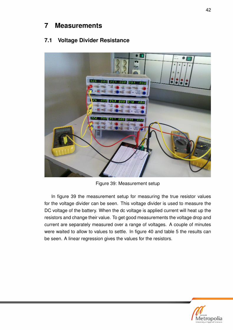
42
7 Measurements
7.1 Voltage Divider Resistance
Figure 39: Measurement setup
In figure 39 the measurement setup for measuring the true resistor valuesfor the voltage divider can be seen. This voltage divider is used to measure theDC voltage of the battery. When the dc voltage is applied current will heat up theresistors and change their value. To get good measurements the voltage drop andcurrent are separately measured over a range of voltages. A couple of minuteswere waited to allow to values to settle. In figure 40 and table 5 the results canbe seen. A linear regression gives the values for the resistors.

43
Figure 40: Linear regression of resistance value
V [V ] V 1[V ](calc.) V 2[V ] I[µA]
97.60 93.23 4.37 103.50
89.80 85.78 4.02 95.25
80.00 76.42 3.58 84.90
70.00 66.87 3.13 74.20
59.90 57.21 2.688 63.60
50.00 47.76 2.241 53.00
40.00 38.21 1.793 42.40
30.10 28.75 1.350 31.90
19.98 19.08 0.895 21.10
10.00 9.55 0.448 10.60
5.00 4.78 0.224 5.30
R1 lin.reg.[kΩ] R2 lin.reg.[kΩ]900.500 4.22
Table 5: Resistance measurement results

44
7.2 Inverter
The generated PWM is filtered using a RC low pass filter with R = 50kΩ andC = 8nF .
Figure 41: PWM at 4000 Hz
In figure 41 the generated sinusoidal PWM by the microcontroller can be seen.A lookup table with 12 lookup points is used resulting in the waveform in figure42.
Figure 42: Sine wave 166 Hz with 12 lookup points

45
Figure 43: PWM at 25000 Hz
In figure 43 the generated sinusoidal PWM by the microcontroller can be seen.A lookup table with 42 lookup points is used resulting in the waveform in figure44.
Figure 44: Sine wave 285 Hz with 42 lookup points

46
8 Program
Teensy(I2C Master)
TI C2000Launchpad
Can Bus Controller
Temperature Sensor x3
I2C Communication BusGalvanic isolation
DC Voltage Sensor x1
Mosfet Switches
SPI B
us
Resolver Signal
SPI Bus
Battery
AC Motor
AC Current Sensor x3
ADC Input
GalvanicIsolation
Mosfet Driver with Overcurrent Protection
Figure 45: System communication overview
In figure 45 you can see a system overview of the inverter. The systems inblue are the parts that need to be programmed. Until now the CAN bus com-munication using SPI has been programmed. The I2C communication with thetemperature sensors has been programmed but not successfully tested. Usingthe C2000 launchpad the sinusoidal PWM has been programmed to work in astationary state.The control loop has still to be implemented. The resolver information via SPIhas to be programmed. The I2C routine to read the DC voltage has to be pro-grammed.

47
9 Summary and Conclusion
In this thesis the theory of controlling a permanent magnet synchronous motorshas been introduced. The control loop of the inverter was shown and direct torquecontrol and field oriented control were discussed. A low voltage mosfet inverterwas built. The sinusoidal pulse width modulation was programmed and tested.Most of the parts of a inverter were discussed. Ways to design and calculate adriver for a mosfet or igbt were shown. The components used in the project weremostly taken from the inventory of the university’s laboratory. Thus the cost waskept lower than 150 e.
As an outline into the future of this project the following points are considered.The control equations to design a PI controller have to be discussed.The low voltage mosfet inverter has to be further tested and programmed.A field oriented control can then be implemented and tested on a low voltage in-verter.The low voltage mosfet inverter was mostly built with through hole components.To keep parasitic capacitances and inductances as low as possible the final in-verter should be designed using small outline components.

48
List of Figures
1 Formula Student logos . . . . . . . . . . . . . . . . . . . . . . . . . 32 Metropolia Motorsport logo . . . . . . . . . . . . . . . . . . . . . . 33 System Overview . . . . . . . . . . . . . . . . . . . . . . . . . . . . 44 Taxonomy of AC motors . . . . . . . . . . . . . . . . . . . . . . . . 65 (a) Continuous Counter EMF of a PMSM, (b) Trapezoidal Counter
EMF of a BLDC . . . . . . . . . . . . . . . . . . . . . . . . . . . . . 76 Typical PMSM structures: (a) surface magnet, (b) inset magnet,
(c) pole shoe rotor, (d) tangentially embedded magnets, (e) radiallyembedded magnets (flux-concentration), (f) two magnets per polein the V position, (g) a synchronous reluctance motor equippedwith permanent magnets.[8, p. 397] . . . . . . . . . . . . . . . . . 8
7 Structure of the Metropolia Motorsport’s motor: interior magnet . . 98 Simplified equivalent circuit of a 3 Phase AC motor. . . . . . . . . . 119 Stationary equivalent circuit of a PMSM (one phase) . . . . . . . . 1210 Square wave conversion . . . . . . . . . . . . . . . . . . . . . . . . 1511 Square wave amplitude spectrum . . . . . . . . . . . . . . . . . . . 1612 Modified sine wave conversion . . . . . . . . . . . . . . . . . . . . 1613 Modified sine wave amplitude spectrum . . . . . . . . . . . . . . . 1714 Simulated PWM signal for a pure sine wave . . . . . . . . . . . . . 1715 Simulated PWM signal for a pure sine wave amplitude spectrum . 1816 Stationary frame of the three phases abc with overlayed stationary
α,β frame (a), Space dector diagram (b) . . . . . . . . . . . . . . . 1917 Space vector synthesizing . . . . . . . . . . . . . . . . . . . . . . . 1918 Control loop overview . . . . . . . . . . . . . . . . . . . . . . . . . 2119 Clarke and Park transformation [7, p. 9] . . . . . . . . . . . . . . . 2320 (a) Equivalent MOSFET representation including junction capaci-
tances; and (b) representation of this physical location.[9, p. 83] . . 2421 The IGBT (a) half-cell vertical cross section and equivalent circuit
model[9, p. 102], (b) IGBT capacitances . . . . . . . . . . . . . . . 2522 (a) Simplified gate charge waveforms, (b) Gate charge character-
istic [5, p. 2] . . . . . . . . . . . . . . . . . . . . . . . . . . . . . . . 2623 Matlab simulation of space vector pwm . . . . . . . . . . . . . . . . 2724 Power supply schematic . . . . . . . . . . . . . . . . . . . . . . . . 2825 Teensy2++ schematic . . . . . . . . . . . . . . . . . . . . . . . . . 2926 C2000 launchpad schematic . . . . . . . . . . . . . . . . . . . . . 2927 Optocoupler module schematic . . . . . . . . . . . . . . . . . . . . 3028 CAN bus module schematic . . . . . . . . . . . . . . . . . . . . . . 30

49
29 Mosfet inverter module schematic . . . . . . . . . . . . . . . . . . 3130 Resolver to digital converter module schematic . . . . . . . . . . . 3231 Modules of the mosfet inverter . . . . . . . . . . . . . . . . . . . . 3332 Mosfet driver schematic . . . . . . . . . . . . . . . . . . . . . . . . 3533 (a)Igbt dynamic gate charge, (b VGE vs. current) . . . . . . . . . . 3734 Short circuit protection logic circuit . . . . . . . . . . . . . . . . . . 3835 RCD snubber circuit . . . . . . . . . . . . . . . . . . . . . . . . . . 3936 C2000 Launchpad . . . . . . . . . . . . . . . . . . . . . . . . . . . 4037 Temperature Sensor SE95DP from NXP . . . . . . . . . . . . . . . 4038 Current Sensor HAIS-50-P and HAIS-100-P from LEM used for
current measurement. . . . . . . . . . . . . . . . . . . . . . . . . . 4039 Measurement setup . . . . . . . . . . . . . . . . . . . . . . . . . . 4240 Linear regression of resistance value . . . . . . . . . . . . . . . . . 4341 PWM at 4000 Hz . . . . . . . . . . . . . . . . . . . . . . . . . . . . 4442 Sine wave 166 Hz with 12 lookup points . . . . . . . . . . . . . . . 4443 PWM at 25000 Hz . . . . . . . . . . . . . . . . . . . . . . . . . . . 4544 Sine wave 285 Hz with 42 lookup points . . . . . . . . . . . . . . . 4545 System communication overview . . . . . . . . . . . . . . . . . . . 46

50
List of Tables
1 PMSM parameter overview . . . . . . . . . . . . . . . . . . . . . . 102 PMSM dynamic equations[4, p. 154] . . . . . . . . . . . . . . . . . 133 Comparison between DTC and FOC . . . . . . . . . . . . . . . . . 224 Bootstrap driver parameters . . . . . . . . . . . . . . . . . . . . . . 355 Resistance measurement results . . . . . . . . . . . . . . . . . . . 43

51
References
[1] Metropolia Motorsport Team History, 2013. http://
metropolia-motorsport.fi/team/team-history/; accessed 20.05.2013.
[2] Zsolt Borkai. About FSHungary, 2012. http://fshungary.hu/
about-fshungary; accessed 20.05.2013.
[3] Rolf Fischer. Elektrische Maschinen 15. edition. HANSER, Munchen, 2011.
[4] Kwang Hee Nam. AC Motor Control and Electric Vehivle Applications. CRCPress, New York, 2010.
[5] Markus Hermwille. Igbt driver calculation. Technical report, Semicron,2007. http://www.semikron.com/skcompub/en/AN-7004_IGBT_Driver_
Calculation_rev00.pdf.
[6] SAE International. 2013 Formula SAE Rules, 2012. http://students.sae.org/competitions/formulaseries/rules/2013fsaerules.pdf.
[7] Microsemi. Field oriented control of permanent magnet synchronous motors.Technical report, Microsemi Cooperation, 2012. http://www.actel.com/
documents/SF_FOC_PMSM_HALL_UG.pdf.
[8] J. Pyrhonen, T. Jokinen, and V. Hrabovcova. Design of Rotating ElectricalMaschines. Wiley, Chichester, UK, 2008.
[9] Muhammad H. Rashid. Power Electronics Handbook. Academic Press,2001.
[10] Wikipedia. Direct torque control, June 2013. http://en.wikipedia.org/
wiki/Direct_torque_control.

52
A Matlab Code
A.1 Matlab code for square wave generation
freq = 1; % Base Frequency
fs=freq*1000; % Sampling frequency
A = 1; % Amplitude
t = 0:1/fs:32/freq;
y = A* square(2*pi*freq*t);
figure(1);
clf(1,'reset');
plot(t,y);
axis([0 2/freq −1.2*A 1.5*A]);
xlabel('Time [s]');
ylabel('Voltage[V]');
title('SquareWave');
set(gcf,'color','w'); %set background to white
%set(gca,'XTick',0:pi/4:2*pi)
%set(gca,'XTickLabel','0','pi/4','pi/2','3/4pi','pi','5/4pi','6/4pi...','7/4pi','2pi')
% Fast Fourier Transform of Square Wave
L = length(y); %Length of Signal
NFFT = 2ˆnextpow2(L); % Next power of 2 from length of signal => FFT...
length
FFT = fft(y,NFFT)/L;
%FFT is symmetric => through away second half
FFT=FFT(1:NFFT/2+1); %+1 ?
%Take the magnitude of FFT
mFFT=2*abs(FFT);
%create frequence vector
f = fs/2*linspace(0,1,NFFT/2+1);%(0:NFFT/2−1)*fs/NFFT;
% Plot single−sided amplitude spectrum.
figure(2);
clf(2,'reset');
plot(f,mFFT);
title('Amplitude Spectrum of SquareWave');
xlabel('Frequency [Hz]');
ylabel(' |Voltage[V] |');set(gcf,'color','w');%set background to white
axis([0 10*freq 0 1.2*A]);

53
A.2 Matlab code for modified sine wave generation
clf(1,'reset');
clf(2,'reset');
freq = 1; % Base Frequency
fs=freq*10000; % Sampling frequency
A = 1; % Amplitude
n= 20; %n Periods
%D = [2.5 10 17.5 20]' * 1/freq; % pulse delay times
D= 0.25*1/freq:1/freq:n/freq;
D2=0.75*1/freq:1/freq:n/freq;
t = 0 : 1/fs : n/freq; % signal evaluation time
w = 0.25*1/freq; % width of each pulse
y = A*(pulstran(t,D,'rectpuls',w)−pulstran(t,D2,'rectpuls',w));
figure(1);
plot(t,y);
axis([0 2/freq −1.2*A 1.2*A]);
xlabel('Time [s]');
ylabel('Voltage[V]');
title('Modified Sinus Wave');
set(gcf,'color','w'); %set background to white
% Fast Fourier Transform of Square Wave
L = length(y); %Length of Signal
NFFT = 2ˆnextpow2(L); % Next power of 2 from length of signal => FFT...
length
FFT = fft(y,NFFT)/L;
%FFT is symmetric => through away second half
FFT=FFT(1:NFFT/2+1); %+1 ?
%Take the magnitude of FFT
mFFT=2*abs(FFT);
%create frequence vector
f = fs/2*linspace(0,1,NFFT/2+1);%(0:NFFT/2−1)*fs/NFFT;
% Plot single−sided amplitude spectrum.
figure(2);
plot(f,mFFT);
title('Amplitude Spectrum of Modified Sine Wave');
xlabel('Frequency [Hz]');
ylabel(' |Voltage[V] |');set(gcf,'color','w');%set background to white
axis([0 10*freq 0 A]);

54
A.3 Matlab code for pure sine wave generation
sinfreq = 1;% Base Frequency
fs = sinfreq*10000; %sampling frequency
fc = 20; %carrying frequency
A=1; %Amplitude
t = 0:1/fs:32/sinfreq;
desired pos signal = A*sin(2*pi*sinfreq*t);
carrying signal = A*sawtooth(2*pi*fc*t,0.5);
desired vel signal = zeros(size(desired pos signal));
desired vel signal = sign(diff(desired pos signal));
PWM = zeros(size(desired pos signal)); %fill PWM with zeros
figure(1)
clf(1,'reset');
plot(t,carrying signal,'g');
hold on
for k= 1:length(desired pos signal)
if carrying signal(k) > desired pos signal(k)
PWM(k)=−1;elseif carrying signal(k) < desired pos signal(k)
PWM(k)=1;
end
end
plot(t,desired pos signal)
hold on
plot(t,PWM,'r')
title('Pure Sine Wave PWM switching');
xlabel('Time [s]');
ylabel(' |Voltage[V] |');axis([0 1 −1.2 1.2]);
set(gcf,'color','w'); %set background to white
annotation('textbox',...
[0.001 0.817 0.095 0.072],...
'String','Vdc',...'LineStyle','none');
annotation('textbox',...
[0.001 0.49 0.095 0.072],...
'String','Vdc/2',...'LineStyle','none');
y = PWM;
% Fast Fourier Transform

55
L = length(y); %Length of Signal
NFFT = 2ˆnextpow2(L); % Next power of 2 from length of signal => FFT...
length
FFT = fft(y,NFFT)/L;
%FFT is symmetric => through away second half
FFT=FFT(1:NFFT/2+1); %+1 ?
%Take the magnitude of FFT
mFFT=2*abs(FFT);
%create frequence vector
f = fs/2*linspace(0,1,NFFT/2+1);%(0:NFFT/2−1)*fs/NFFT;
% Plot single−sided amplitude spectrum.
figure(2);
clf(2,'reset');
plot(f,mFFT);
title('Amplitude Spectrum of sine wave');
xlabel('Frequency [Hz]');
ylabel(' |Voltage[V] |');set(gcf,'color','w');%set background to white
axis([0 100*sinfreq 0 A]);

56
A.4 Matlab code for space vector PWM
function [S1,S2,S3,S4,S5,S6,sector,t1]=fcn(vd e,vq e,ramptime,...
theta e,Ts,Vdc)
S1=3;S2=3;S3=3;S4=3;S5=3;S6=3; %switching fault state values
%transform from synchronous into stationary frame
vd s=cos(theta e)*vd e−sin(theta e)*vd e;
vq s=sin(theta e)*vq e+cos(theta e)*vq e;
%find sector number in hexagon
if(vq s > 0)
if(abs(vq s) > (sqrt(3)*abs(vd s)) )
sector=2;
elseif(vd s > 0)
sector=1;
else
sector=3;
end;
elseif(abs(vq s) > (sqrt(3)*abs(vd s)))
sector=5;
elseif(vd s > 0)
sector=6;
else
sector=4;
end;
%calculate T1,T2 duties for each sector to generate relation between...
d,q
T1=sqrt(3)*Ts/(Vdc)*(sin(pi/3*sector)*vd s−cos(pi/3*sector)*vq s);
T2=sqrt(3)*Ts/(Vdc)*(−sin(pi/3*(sector−1))*vd s+cos(pi/3*(sector−1)...)*vq s);
T0 =Ts−(T1+T2);t1=[T0/4 T1 T2 T0/4 T0/4 T2 T1 T0/4];t1=cumsum(t1);
%sector I
if(sector==1)
pwmS1=[0 1 1 1 1 1 1 0];pwmS3=[0 0 1 1 1 1 0 0];pwmS5=[0 0 0 1 1...
0 0 0];
pwmS4=[1 0 0 0 0 0 0 1];pwmS6=[1 1 0 0 0 0 1 1];pwmS2=[1 1 1 0 0...
1 1 1];
for j=1:8
if(ramptime<t1(j))

57
break;
end;
end;
S1=pwmS1(j);S3=pwmS3(j);S5=pwmS5(j);
S4=pwmS4(j);S6=pwmS6(j);S2=pwmS2(j);
end;
% sector II
if(sector==2)
pwmS1=[0 0 1 1 1 1 0 0];pwmS3=[0 1 1 1 1 1 1 0];pwmS5=[0 0 0 1 1...
0 0 0];
pwmS4=[1 1 0 0 0 0 1 1];pwmS6=[1 0 0 0 0 0 0 1];pwmS2=[1 1 1 0 0...
1 1 1];
for j=1:8
if(ramptime<t1(j))
break;
end;
end;
S1=pwmS1(j);S3=pwmS3(j);S5=pwmS5(j);
S4=pwmS4(j);S6=pwmS6(j);S2=pwmS2(j);
end;
%sector III
if(sector==3)
pwmS1=[0 0 0 1 1 0 0 0];pwmS3=[0 1 1 1 1 1 1 0];pwmS5=[0 0 1 1 1...
1 0 0];
pwmS4=[1 1 1 0 0 1 1 1];pwmS6=[1 0 0 0 0 0 0 1];pwmS2=[1 1 0 0 0...
0 1 1];
for j=1:8
if(ramptime<t1(j))
break;
end;
end;
S1=pwmS1(j);S3=pwmS3(j);S5=pwmS5(j);
S4=pwmS4(j);S6=pwmS6(j);S2=pwmS2(j);
end;
%sector IV
if(sector==4)
pwmS1=[0 0 0 1 1 0 0 0];pwmS3=[0 0 1 1 1 1 0 0];pwmS5=[0 1 1 1 1...
1 1 0];
pwmS4=[1 1 1 0 0 1 1 1];pwmS6=[1 1 0 0 0 0 1 1];pwmS2=[1 0 0 0 0...
0 0 1];

58
for j=1:8
if(ramptime<t1(j))
break;
end;
end;
S1=pwmS1(j);S3=pwmS3(j);S5=pwmS5(j);
S4=pwmS4(j);S6=pwmS6(j);S2=pwmS2(j);
end;
% sector V
if(sector==5)
pwmS1=[0 0 1 1 1 1 0 0];pwmS3=[0 0 0 1 1 0 0 0];pwmS5=[0 1 1 1 1...
1 1 0];
pwmS4=[1 1 0 0 0 0 1 1];pwmS6=[1 1 1 0 0 1 1 1];pwmS2=[1 0 0 0 0...
0 0 1];
for j=1:8
if(ramptime<t1(j))
break;
end;
end;
S1=pwmS1(j);S3=pwmS3(j);S5=pwmS5(j);
S4=pwmS4(j);S6=pwmS6(j);S2=pwmS2(j);
end;
%Sector VI
if(sector==6)
pwmS1=[0 1 1 1 1 1 1 0];pwmS3=[0 0 0 1 1 0 0 0];pwmS5=[0 0 1 1 1...
1 0 0];
pwmS4=[1 0 0 0 0 0 0 1];pwmS6=[1 1 1 0 0 1 1 1];pwmS2=[1 1 0 0 0...
0 1 1];
for j=1:8
if(ramptime<t1(j))
break;
end;
end;
S1=pwmS1(j);S3=pwmS3(j);S5=pwmS5(j);
S4=pwmS4(j);S6=pwmS6(j);S2=pwmS2(j);
end;