Embed Size (px)
Citation preview

Case History: Development of a Bluetooth Transceiver in RF CMOSBy Bob Koupal & Marshall Wang, Signia Technologies
& Cory Edelman, Agilent Technologies
The design of Signia Technologies’ Ulysses SBT5010 2.4-GHz Bluetooth transceiver requiredspecial attention to achieve its design using a low-cost CMOS RFIC process. Key performancecriteria were evaluated at all stages of the design process using EDA software that includedintegrated foundry models, system-compliance test templates for Bluetooth test signals and linksto test instruments to verify that measured results agreed with simulation data.
The Bluetooth standard was established for short-range wireless transceivers that are embeddedin a wide range of devices, including notebook computers, printers, fax machines, cameras, cell-phones, head-sets, home appliances, PDAs and other portable devices. Manufacturers of thesedevices require that the addition of Bluetooth be accomplished with small size, low powerconsumption and low cost. To meet this demand, a System-on-Chip (SoC) solution using a highlevel of integration is required. The goal of SoC is to eliminate expensive external componentssuch as surface acoustic wave (SAW) filters and inductors, to minimize the number of externalpassive components and reduce overall cost, eliminating external RF tuning elements to simplifyimplementation.
Interference is a significant design issue for Bluetooth radio links, which operate in the non-licensed 2.4-GHz ISM band with a signal that is frequency hopped over eighty 1-MHz channelsat a rate of 1600 hops per second. Bluetooth links must have reliable operation in the presence ofother RF emitters in the 2.4-GHz band, including other Bluetooth devices, cordless telephones,microwave ovens and wireless LAN systems such as those using the IEEE 802.11 standard.
A single-chip radio has been the stated goal for many wireless standards, including GSM andCDMA phones, but Bluetooth is the first standard to truly demand it to be successfullyimplemented in high volumes, with small size and low cost. Bluetooth IC designs requireincreasing levels of complexity as radio, mixed-signal and digital functional blocks are combinedon a single piece of silicon.
The Signia Two-Chip SolutionSignia Technologies has implemented a Bluetooth SoC solution on two chips, a 2.4 GHztransceiver RFIC (see Fig. 1) and a baseband controller IC. This approach optimizes the Bill ofMaterials (BOM) costs, with the flexibility to address a number of applications. The radio ICincludes a cascode-type low-noise amplifier (LNA) with a source-degenerating inductor fornoise matching and a 50-Ω input impedance. The LNA has a 4-dB noise figure, 15-dB gain and a-10 dBm input third-order intercept point (IIP3.) The receiver also includes an IF filter, mixerand demodulator. The transmitter includes a mixer, filter and power amplifier (PA.) The PA ismatched to 50 Ω using an on-chip high-Q inductor and delivers 20-dB gain, +8 dBm P1dB, and apower-added-efficiency of 15% at P1dB.

Fig. 1: The Signia Ulysses SBT5010 Bluetooth TxRx showing the primary simulationmethods used for each block
The chip also includes a Gaussian Frequency-Shift Keyed (GFSK) modulator/demodulator, a2.4-GHz PLL controlling a quadrature voltage-controlled-oscillator (VCO), tunable IF filters,digital clock recovery circuitry, dc estimation and control logic. The VCO is implementedcompletely on the RFIC with an on-chip resonator and frequency-tuning varactors. The VCOconsumes only 5 mA, and its single-sideband phase noise has 10 to 15 dB margin beyond thelevel required by the Bluetooth specification. The baseband IC (not covered in this article)contains the entire core Bluetooth functionality, with interfaces for USB, UART, and aninnovative host interface that allows the controller to be configured for PCMCIA, parallel/printerport, and PCI interfaces without the need for additional components. The two chips communicatethrough an 8-pin BlueRF mode-2 bi-directional interface.
Bluetooth RF Design IssuesComplexity, combined with cost-related goals, requires that the design of a Bluetooth radio SoCtake a different approach to simulation and layout. Traditional RF building-block design wouldstart with components, then develop a circuit topology, which is analyzed using harmonicbalance or circuit envelope simulation. This sequential design method does not work for SoCdesign; instead, several disciplines are applied simultaneously, since portions of the circuit arehigh-frequency analog, portions are mixed-signal, and the remainder are purely digital. Someparts require linear, nonlinear or electromagnetic RF simulation, others require both SPICE-likesimulations and Verilog for timing analysis, while some require only Verilog simulation. In thisdesign, there are several hundred active components in the analog portion, and over 30,000 gateson the digital side. The complexity of this design prevents the designer from using a single EDAtool for simulating the entire chip: System-level planning must ensure that the individual blocksare specified correctly and simulated using the right technologies.
Power and noise budgets are among the first, and most important, system parameters that defineperformance. Bluetooth is nominally a 1-mW (0-dBm) system, using GFSK modulation in a 1-MHz bandwidth. Together with a 0.1% Bit Error Rate (BER) requirement, this implies a Carrier-to-Noise (C/N) ratio of 21 dB. The thermal noise floor for a 1-MHz bandwidth is -114 dBm, andthe Bluetooth specification demands a receiver sensitivity of -70 dBm or better, or a receivernoise figure of 23 dB, which is based on the typical transmitted signal level at a range of 10 m.

However, realistic applications of Bluetooth require 10 to 15 dB better receiver sensitivity toovercome the effects of the difficult indoor propagation environment (see Fig. 2.)
Fig. 2: The signal and noise level relationships governing Bluetooth receiver performance
For the requirements of Bluetooth, there are several options for a process technology:• Complementary Metal-Oxide Semiconductor (CMOS)• Bipolar-CMOS (BiCMOS)• Silicon-on-Insulator (SoI)• Silicon-Germanium (SiGe)
Of these processes the lowest cost is CMOS. For example, the 0.25-µm CMOS process providedby Taiwan Semiconductor Manufacturing Company Ltd. (TSMC) and other companies istypically 30 to 50% lower in cost than BiCMOS because it requires fewer mask and processsteps. SoI and SiGe have more expensive starting materials and more complex processes. CMOSachieves its low cost though high volume, and there are many foundries with available capacity.
To produce the RF blocks necessary for radio system design, TSMC’s well-established 0.25 µmprocess provides an fT of more than 30 GHz, which enables the design of the required Bluetoothbuilding blocks – a 3.5-dB noise figure LNA with 20 dB of small signal gain, a fully integratedVCO with quadrature output and phase noise better than –95 dBc/Hz at 500-kHz offset, and a
fully integrated 10-dBm PA with 30% efficiency. The process has been tailored for analog RFdesign, with features that include thick top metal for fabrication of high-Q inductors andtransformers, metal-insulator-metal (MIM) capacitors, multiple VT devices and varactor diodes.The process also has deep-n-well structures that improve device isolation.
The overall system architecture is the next step in the design phase. Beginning with the receiver,we recall that Bluetooth specifications require at least a –70 dBm sensitivity with a BER of0.1%, even with interference present, with –80 dBm or better needed for most applications. Forcost and manufacturability this performance must be achieved with a minimal number ofexternal components. There are 3 basic receiver architectures that might be considered, each withits own advantages and limitations:
• Traditional superhetrodyne (see Fig. 3) – The superhetrodyne topology easily meets theelectrical requirements. They have high channel selectivity and are well understood circuits,but require external SAW filters making them too expensive for Bluetooth requirements.
Fig. 3: Superhetrodyne receiver architecture
• Zero-IF (see Fig. 4) – Zero-IF designs allow high levels of integration and eliminate the needfor an image filter, but have poor rejection of local oscillator (LO) feed-through and can havedc offsets on the outputs, making zero-IF a relatively complex design to implement.
Fig. 4: Zero-IF receiver architecture
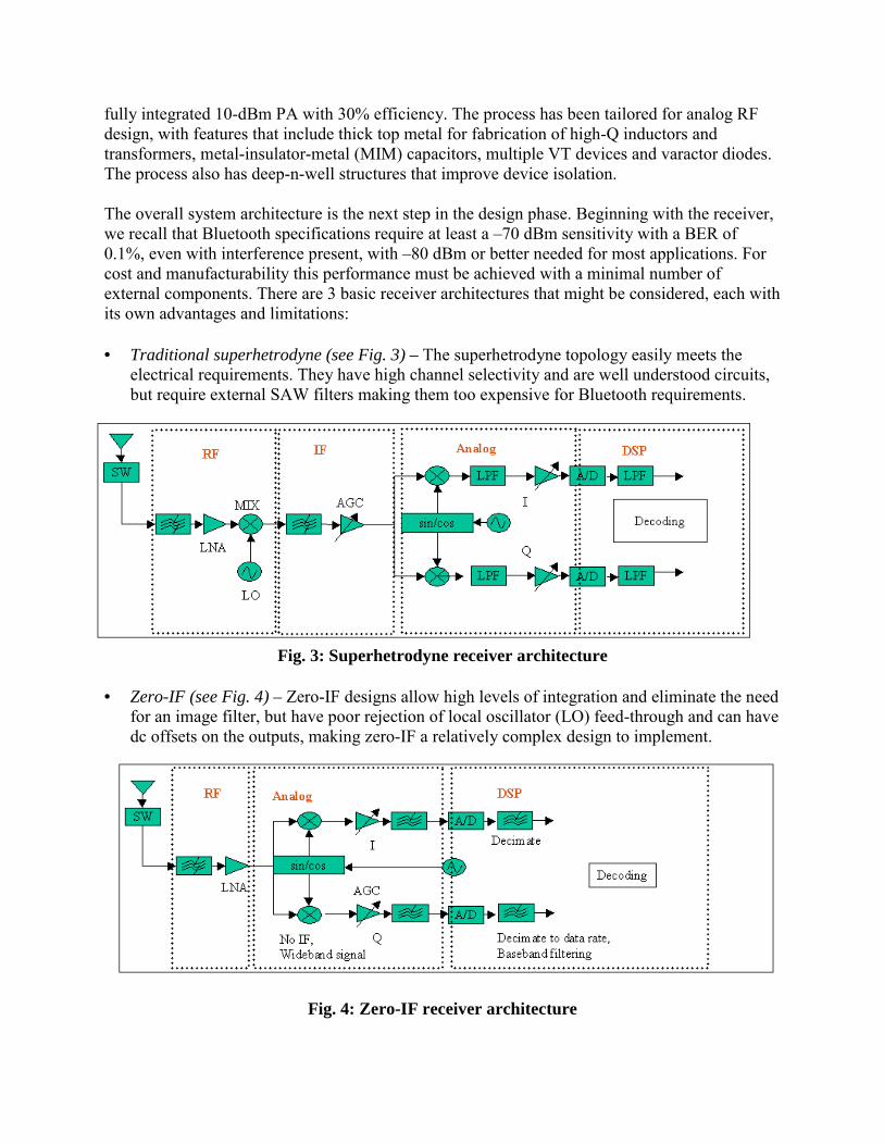
• Low-IF (see Fig. 5) – Low-IF was selected by Signia, a design architecture that also supportshigh levels of integration and eliminates the need for external filters, but is simpler toimplement than the zero-IF approach, and leads to higher yields and lower cost.
Fig. 5: Low-IF receiver architecture
Once the low-IF receiver architecture was selected, the next decision was whether to use limiter-based or I-Q demodulation. I-Q receivers are commonly used in digital communication circuitsfor QPSK demodulation, but require accurate quadrature LO signals and a high-linearity AGCamplifier. The limiter-based method is well suited for 2-FSK applications and, without needingan AGC amplifier, is much simpler to implement, which lowers the cost. Another design choicewas a matched 50-Ω receiver front-end that did not require external matching networks. Theentire low-IF topology was verified in simulation and optimized for the desired performanceusing high-level behavioral blocks included in the Bluetooth DesignGuide which is part ofAgilent EEsof EDA's Advanced Design System 2001 (ADS 2001.)
The Bluetooth transmitter specification permits three levels of output power: 0 dBm (Class 3),+4 dBm (Class 2), and +20 dBm (Class 1.) Class 1 enables a range up to 150 meters, and its +20dBm power level is usually going to be implemented with an external PA. In this design, carewas taken to keep the 2-MHz spur of the transmitter below –40 dBc to stay within specificationsif an external PA is added. To determine the optimum transmitter topology two approaches wereconsidered: Direct VCO modulation and I-Q modulation. The direct VCO approach is attractivebecause it a simpler design and requires less current, but it is prone to problems with frequencydrift and variation of the modulation index. The approach selected for this design was I-Qmodulation, which effectively eliminates frequency drift problems and allows direct modulationusing I and Q signals derived from the baseband IC. As with the receiver, the entire transmittopology was verified using Bluetooth DesignGuide in ADS.
Simulation And Verification Of The DesignsRF circuits designed to fit the selected topologies were initially simulated using the ADSharmonic balance simulator, in conjunction with a Design Kit that includes RF models providedby TSMC. The Design Kit has symbols created for each supported device type in the TSMClibrary, including corner models. The devices include a variety of BSIM3 models for nMOS and
pMOS transistors, MIM capacitors, a number of polysilicon and diffused resistors, inductors,varactors and other diodes.
To derive on-chip baluns or specific inductor values that are not supported by the Design Kit, thedevices are designed separately and the file then attached to a symbol for use in simulation. Theyare first laid out using Cadence Analog Artist, then imported into ADS’s Momentum RF 2.5Delectromagnetic simulator. Pins are added to the layout to define the current flow direction, thepolygons are meshed into rectangles and triangles, and the dielectric properties of the substrateare defined. The circuit is then simulated using the planar field solver, and the S-parameters arecreated and stored in a model file.
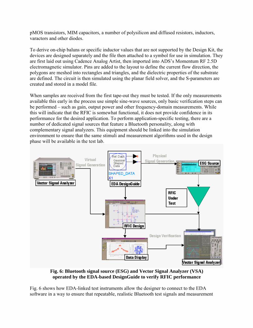
When samples are received from the first tape-out they must be tested. If the only measurementsavailable this early in the process use simple sine-wave sources, only basic verification steps canbe performed – such as gain, output power and other frequency-domain measurements. Whilethis will indicate that the RFIC is somewhat functional, it does not provide confidence in itsperformance for the desired application. To perform application-specific testing, there are anumber of dedicated signal sources that feature a Bluetooth personality, along withcomplementary signal analyzers. This equipment should be linked into the simulationenvironment to ensure that the same stimuli and measurement algorithms used in the designphase will be available in the test lab.
Fig. 6: Bluetooth signal source (ESG) and Vector Signal Analyzer (VSA)operated by the EDA-based DesignGuide to verify RFIC performance
Fig. 6 shows how EDA-linked test instruments allow the designer to connect to the EDAsoftware in a way to ensure that repeatable, realistic Bluetooth test signals and measurement

algorithms are used for simulation and hardware design. It is also possible to insert simulationmodels into the signal path at any point. These models may be hardware, such as portions of thecircuit that are not part of the RFIC, or they may be signal impairments such as multipath fadingor interfering signals of any type. The Bluetooth 1.1 specification spells out what is required forreceiver performance: Sensitivity, adjacent-channel interference at various frequency offsets, co-channel interference and intermodulation distortion. For each of these tests the system mustachieve a BER of 0.1% (see Fig. 7.) This is the so-called “raw” BER, which does not include anyimprovements gained by error-correcting coding.
Fig. 7: A critical test for the low-IF receiver’s performance is adjacent-channel selectivity

Verifying The Design
Fig. 8: Receiver Sensitivity Template in the EDA environment
Fig. 8 shows a typical test template that combines both the EDA environment and test equipmentfor hardware design and verification. The reference transmitter and/or receiver model is replacedby the circuit under test, which is then compared with the simulated design until the hardwarebecomes available. The signal path may include a simple Additive White Gaussian Noise(AWGN), or Multipath model optimized for indoor propagation. Performance may be observedby using an eye diagram (Fig. 9), a BER measurement (Fig. 10), or via a software-based VectorSignal Analyzer to demodulate the signal and measure modulation accuracy (Fig. 11.)
Fig. 9: Eye diagrams at the test receiver’s demodulated outputwith a -70 dBm input (left) and -84.5 dBm input (right)

Fig. 10: BER vs. received signal power for the candidate receiver, which exceedsthe -70 dBm Bluetooth requirement, and should be usable to -83 dBm

Fig. 11: Vector Signal Analyzer showing the demodulated symbols vs. time, eye diagram,FSK error percent and received data statistics and the signal spectrum
As noted earlier, a variety of simulation technologies must be used for complete and accurateverification. Initial analysis of circuit design can be started using non-linear steady-statetechniques such as harmonic balance. Using single or multiple tones and their harmonics,harmonic balance is applicable to mixers, amplifiers and filters. For I-Q modulation with directup-conversion to the desired transmit frequency it is difficult, if not impossible, to infer thequality of performance using tone excitation; the full I-Q representation of the modulated signalmust be used to drive the modulator. Although a transient simulation can infer some aspects ofmodulator performance, only an circuit envelope simulator can predict it fully. Therefore, theEDA environment must provide either the signal-processing necessary to produce the I-Qrepresentation of the Bluetooth signal and be able to apply the envelopes to the circuit being
evaluated, or that signal must be created ahead of time and stored in a format usable by thecircuit envelope simulator.
Finally, the schematic was transferred to a layout environment and subjected to time-domainsimulation as an additional verification step. Following the layout entry and design rule check, aGDSII stream was produced and sent to the foundry. Finally, the fabricated devices were verifiedin a full transmit or receive configuration, again using the EDA-based test templates andassociated test equipment.
Simulation And Verification ResultsTo review, the simulations were performed using both steady-state and time-domain methods.Harmonic balance techniques were used for the initial design of the I-Q modulator, poweramplifier, LNA and mixer subcircuits. Two time-domain methods were used. First, SPICE wasused to examine transient performance where needed. The Circuit Envelope simulation methodwas used to examine the time-domain co-simulation of complete subcircuits including signalsand measurements, operating in the Agilent Ptolemy-based behavioral signal-processingenvironment. With the appropriate simulation tools available, there was no need to compromiseaccuracy by introducing simplistic behavioral models for the RF subcircuits into the compliancetest templates.
A sample of measured and simulated results for the power amplifier subcircuit of the transceiverare shown in Fig. 12. In this case, measurements of the first-pass design all comfortablyexceeded simulated performance parameters.
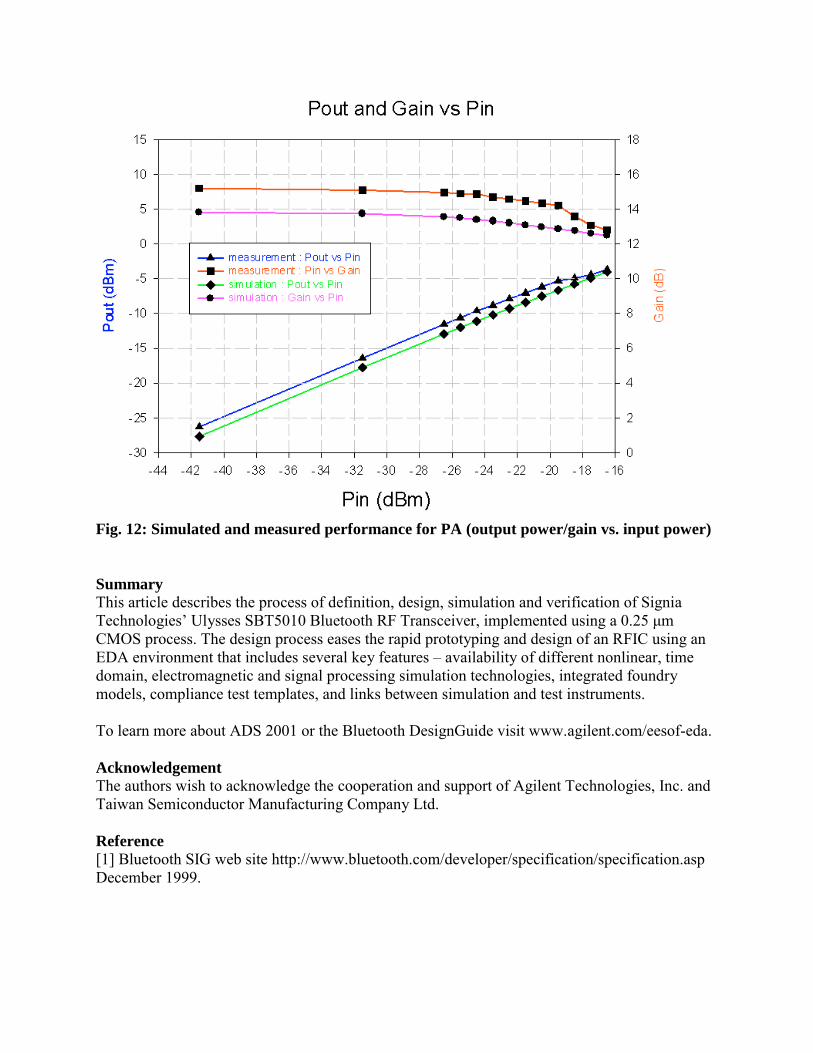
Fig. 12: Simulated and measured performance for PA (output power/gain vs. input power)
SummaryThis article describes the process of definition, design, simulation and verification of SigniaTechnologies’ Ulysses SBT5010 Bluetooth RF Transceiver, implemented using a 0.25 µmCMOS process. The design process eases the rapid prototyping and design of an RFIC using anEDA environment that includes several key features – availability of different nonlinear, timedomain, electromagnetic and signal processing simulation technologies, integrated foundrymodels, compliance test templates, and links between simulation and test instruments.
To learn more about ADS 2001 or the Bluetooth DesignGuide visit www.agilent.com/eesof-eda.
AcknowledgementThe authors wish to acknowledge the cooperation and support of Agilent Technologies, Inc. andTaiwan Semiconductor Manufacturing Company Ltd.
Reference[1] Bluetooth SIG web site http://www.bluetooth.com/developer/specification/specification.aspDecember 1999.