Embed Size (px)
Citation preview
1
DesignCon 2016
100Gbps Dual-channel PAM-4
transmission over Datacenter
Interconnects
Pulkit Khandelwal, Inphi Corp
Jamal Riani, Inphi Corp
Arash Farhoodfar, Inphi Corp
Arun Tiruvur, Inphi Corp
Ishwar Hosagrahar, Inphi Corp
Frank Chang, Inphi Corp
Jennifer Wu, Inphi Corp
Karthik Gopalakrishnan, Inphi Corp
Sameer Herlekar, Inphi Corp
Sudeep Bhoja, Inphi Corp

2
Abstract
This paper highlights a PAM-4 transceiver that achieves 100Gbps Dual Channel
transmission over electrical and optical interconnects used within world’s largest
Datacenters. The transceiver chip, built in 28nm CMOS process, employs a PAM-4
transmitter with 3tap FFE, a PAM-4 receiver with CTLE, ADC and DSP based
equalization and FEC logic.
Measured lab results are presented showing 100G PAM-4 transmission with BER<1E-15
over a IEEE Std. 802.3bj 100GBASE-CR4 compliant 3m 30AWG Direct-Attach Copper
cable used for Server to TOR connections; optical fibers linking the TOR, aggregation
and core switches; and a IEEE Std. 802.3bj 100GBASE-KR4 compliant backplane +
connector solution typically found within layer-3 core switches and/or edge routers.
Author(s) Biography
Pulkit Khandelwal is a Systems Engineer in the Networking Interconnect CTO Office at
Inphi. He is presently a lead contributor on the PAM-4 transceiver technology, working
on chip architecture, analog modelling, design verification and post-Si lab activities
focused on performance evaluation and software development.
Jamal Riani is a Senior Principal Engineer in the Networking Interconnect CTO Office at
Inphi. He is the lead DSP architect on the PAM-4 transceiver ASIC. He has a PhD degree
from Eindhoven University of Technology, The Netherlands and BE and MSEE from
Ecole Polytechnique and Ecole Nationale Superieure de telecommunications-Paris,
France.
Arash Farhoodfar is Sr. Director of Engineering at Inphi, leading the design and
development of high-speed transceiver ASICs. Arash is hands on with designing low-
power and high performance DSP Phys. He is familiar with the end to end process from
concept through design and production.
Arun Tiruvur is Director of Engineering in the Networking Interconnect CTO Office at
Inphi, leading the design and development of high-speed DSP and FEC logic for PAM-4
based applications. He received his B.E, EC from University of Mysore and MSEE from
Kansas State University.
Frank Chang is a Principal Engineer at Inphi CTO Optics Office for Optics
Interconnect. He leads the optical system engineering efforts for physical layer IC
products involving high speed drivers, TIAs and PAM-4 PHYs for various optical
applications. He holds a Ph.D in Optoelectronics from Ecole Polytechnique of University
of Montreal, Canada.
Ishwar Hosagrahar is a Sr. Staff Engineer at Inphi in the Signal Integrity team. He is a
key contributor working on a wide range of SI challenges with both NRZ and PAM-4
SerDes ranging from link simulations/evaluation to lab measurements for correlating

3
algorithmic models. He holds a Masters degree in E.E. (VLSI/Circuits) from University
of Texas.
Jiangfeng (Jennifer) Wu is an Associate Technical Director at Inphi, working on DSP
based broadband transceivers. Prior to Inphi, Jennifer worked for Broadcom as an
Associate Technical Director and Senior Principal Engineer, and other companies in the
area of DSP based transceiver design and implementation. She holds a Ph.D. degree in
E.E. from McMaster University.
Karthik Gopalakrishnan is currently leading the high-speed analog group developing
PAM-4 based solutions for optical and electrical applications. He is a Senior Member of
IEEE and has co-authored several patents and publications. He received his B.E, EE from
Mangalore Univ. and M.S, EE from Michigan State University respectively.
Sameer Herlekar is a Senior Staff Engineer with Inphi, Santa Clara. He has published,
and frequently serves as a reviewer for many leading journals and conferences. Sameer
received his PhD in Electrical Engineering from Louisiana State University, a B.E. in
Electronics and M.Sc. in Mathematics from BITS, Pilani, India.
Sudeep Bhoja has served as Inphi’s CTO, Networking Interconnect since March 2012
and leads the system architecture team responsible for the development of the PAM-4
DSP transceiver IC. Prior to Inphi, he was Technical Director in the Infrastructure and
Networking Group at Broadcom and played an instrumental role in developing 10-
Gigabit Ethernet optical and copper transceivers.

4
1. Introduction
The ongoing trends of rapid growth in cloud computing, web streaming, mobile
applications, search, social media, etc. are creating the need to double the bandwidth
demand in the datacenter every 12-15 months leading to constant evolution of datacenter
architectures [1]. As server processing power and storage capacity continues to ramp up
quickly, the interconnect pipes linking the hundreds of thousands of servers and storage
arrays within a data-center and also cross-connecting multiple datacenters are seen as key
bottlenecks in satisfying this insatiable need for unlimited bandwidth.
Today’s datacenter interconnects are transitioning from 10/40GbE rapidly towards
100GbE, whilst there is clear roadmap forming within IEEE for 50GbE, 200GbE and
400GbE. Current 40GbE and 100GbE physical connections are typically 4x10G, 10x10G
or 4x25G NRZ links. Going forward, PAM-4 modulation has now been recognized as the
modulation scheme that will take the industry over the next wave of Ethernet
deployments for optical and copper interconnects by doubling the bits per symbol at the
same baud rate.
This paper considers the application of PAM-4 transceiver technology at each tier of a so-
called 3-tier switch topology [2] [3], a canonical model of which is illustrated in Figure 1.
At the lowest tier, a cabinet, or rack of servers is connected to a switch at the top of the
rack (ToR). The next higher layer, typically known as the leaf layer, consists of switches
that aggregate traffic from all the ToRs in the datacenter. The interconnects at this layer
are typically multi-mode fibers (MMF) and single-mode fibers (SMFs) covering
distances of up to 500m. At the top-most tier, a spine switch combines traffic from all the
leaf switches. The interconnects between the Leaf and Spine switches are also SMF
optical links spanning distances of up to 2km. Finally, within a Spine switch chassis with
multiple front-plane line cards cross-connected to fabric cards, the traffic is routed
internally over a backplane.
ToR
Leaf
Spine
Server
Rack
Figure 1: Intra-Datacenter 3-Tier Switching Topology

5
The next section describes the overall chip architecture with details on the salient features
of the PAM-4 transmitter and receiver. This is followed by lab results on three setups
representing the datacenter interconnect topology described above, highlighting the
performance of 50Gbps/lane PAM-4 over media currently deployed for 25Gbps/lane
NRZ links.
2. PAM-4 XCVR Architecture
2.1 Top-level Description
A high level block-diagram of the PAM-4 transceiver is illustrated in Figure 2 below,
with the top half constituting the Egress path and the bottom half being Ingress path.
Figure 2: Inphi PAM-4 Transceiver Block Diagram
The Egress path of the transceiver starts with a CAUI-4 25.78125Gbps CEI-28G-VSR
compliant NRZ Receiver (Rx) to interface to the host ASIC. The Ethernet traffic
originating from the host is FEC encoded and transmitted out of the chip as two
25.78125Gbaud PAM-4 data streams. The FEC encoding function can be bypassed if this
function is implemented in the host ASIC. The Transmitter (Tx) architecture is outlined
in Section 2.2. The transceiver implements the IEEE Std. 802.3bj 100GBASE-KR4 and
100GBASE-KP4 FEC schemes.
The Ingress path of the transceiver starts with ADC+DSP based receiver. The details are
outlined in Section 2.3. The output data stream from the DSP is passed on to the FEC
decoder block, which if enabled, recovers the original Ethernet stream. The 100G data is
transmitted back to the host through a CAUI-4 25.78125Gbps CEI-28G-VSR compliant
NRZ Tx.
In addition the chip implements both MDIO and I2C management interfaces to program
registers for device configuration and diagnostic features.
6
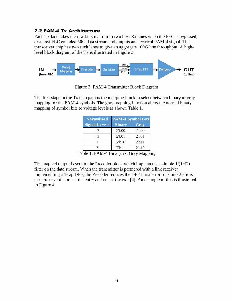
2.2 PAM-4 Tx Architecture
Each Tx lane takes the raw bit stream from two host Rx lanes when the FEC is bypassed,
or a post-FEC encoded 50G data stream and outputs an electrical PAM-4 signal. The
transceiver chip has two such lanes to give an aggregate 100G line throughput. A high-
level block diagram of the Tx is illustrated in Figure 3.
Figure 3: PAM-4 Transmitter Block Diagram
The first stage in the Tx data path is the mapping block to select between binary or gray
mapping for the PAM-4 symbols. The gray mapping function alters the normal binary
mapping of symbol bits to voltage levels as shown Table 1.
Table 1: PAM-4 Binary vs. Gray Mapping
The mapped output is sent to the Precoder block which implements a simple 1/(1+D)
filter on the data stream. When the transmitter is partnered with a link receiver
implementing a 1-tap DFE, the Precoder reduces the DFE burst error runs into 2 errors
per error event – one at the entry and one at the exit [4]. An example of this is illustrated
in Figure 4.
Binary Gray
-3 2'b00 2'b00
-1 2'b01 2'b01
1 2'b10 2'b11
3 2'b11 2'b10
Normalised
Signal Levels
PAM-4 Symbol Bits

7
Figure 4: Tx Precoder Example (Courtesy: [4])
This is followed by a Serializer block which generates individual pre-cursor, main-cursor
and post-cursor serialized PAM-4 symbol stream to the 3-tap FIR filter. The FIR filter
has independent control on the PAM-4 MSB and LSB paths. Overall, the filter
coefficients can range from 0 to -0.25 for the pre-cursor and from 0 to -0.5 for the post-
cursor.
The FIR output is fed into an output driver which provides swing levels up to 1.4Vppd.
The MSB to LSB ratio can also be altered for providing pre-distortion on the PAM-4 eye,
which is useful in applications where the PAM transmitter interfaces with optical drivers.
Measured PAM-4 eye diagrams from the Tx are shown in Figure 5 showing a 1V ppd
signal with no pre-cursor and post-cursor FIR coefficients and with an example pre-
cursor and post-cursor taps both set to -0.15.

8
Figure 5: PAM-4 Tx Measured Eye Diagrams at Tx FIR [pre main post] coefficients of
[0 1 0] on the left and [-0.15 0.7 -0.15] on the right
2.3 PAM-4 Rx Architecture
The transceiver chip has two Rx lanes to give an aggregate 100G line throughput. The
block diagram of the ADC+DSP Receiver is shown in Figure 6.
Figure 6: PAM-4 Receiver Block Diagram
The Rx signal terminates with 50ohms at the Continuous-time Linear Equalizer (CTLE)
block. The CTLE provides a programmable high-frequency boost ranging from 0dB to
8dB. It also has a gain range >12dB in 0.1dB steps to scale the input signal voltage to
match the ADC input swing requirements. The CTLE drives the Track-and-Hold (T/H)
and a 7-bit time-interleaved ADC which can operate up to 28GSamples/Sec.
The clocking for the T/H and ADC is derived from a PLL operating off an external
reference clock. The PLL block takes timing recovery controls from the DSP to track the
phase variations of the incoming data.
The DSP core employs a set of parallel FFE slices for channel equalization. The parallel
factor which is chosen to be a multiple of the number of sub-channels in the time

9
interleaved ADC allows for any bandwidth mismatch between the different AFE paths to
be compensated by independent adaptation of the FFE slices.
Following the FFE, the DSP can optionally enable an adaptive PAM-4 Decision
Feedback Equalizer (DFE). The feedback taps are limited to 1 tap to reduce the impact of
error propagation. The inverse of the Tx Precoder is implemented after the DFE.
For timing recovery, the DSP implements a baud-rate CDR which is based on the well-
known Mueller-Muller [5] scheme taking inputs directly at the ADC output, thus
eliminating interaction problems with other DSP blocks.
The DSP bring-up and link training are handled by a combination of Finite State
Machines implemented in hardware and firmware running on an on-chip micro-
controller.
For link training and diagnostics, the DSP has a Signal-to-Noise Ratio (SNR) monitor
block. The SNR is derived from calculating the mean square of the error signal which is
simply the delta between the slicer input and the ideal PAM-4 expected levels.
The Slicer Histogram block further enhances link diagnostic capabilities by giving more
details of the distribution of samples at the final Slicer around the 4 signal amplitude
levels. This is accomplished by counting the number of hits at the Slicer within a finite
number of discrete bins (effectively determining a certain voltage resolution). Figure 7
depicts a typical output of the block. The x-axis is address of the bins indicating the
PAM-4 levels. The y-axis is simply a count of the number of hits within each bin. This
data can be captured in real-time without interrupting traffic and represents true slicer
margin at the sampling phase.
Figure 7: Example output from Slicer Histogram Block
A more conventional post-equalized eye diagram at the final slicer can be obtained by
stitching the slicer histogram data at timing recovery phases swept over the entire UI,
even over asynchronous links. An example is shown in Figure 8.

10
Figure 8: Example post-equalized PAM-4 eye at Rx slicer
3. PAM-4 Evaluation in Cloud Data Centre Applications
3.1 Server to TOR Switch Interconnect using Direct-Attach
Copper Cable
3.1.1 Objective
This section covers the application of PAM-4 over a ToR architecture where each server
in the rack is typically connected via a QSFP28 Direct-Attach Copper (DAC) cable to a
so-called ToR switch which is physically located within the cabinet, often at the top of
the rack as illustrated in Figure 9.
In current 100G deployments, the DAC cable assemblies with QSFP28 mating interfaces
feature eight differential copper pairs, providing four data transmission channels at
speeds of up to 28Gbps per channel. The reach in these applications is usually 3 to 5
meters and trade-offs are often made between wire gauges, length and cost depending on
the application. The overall link insertion loss budgets spanning the Server board and
Switch board traces are defined in the IEEE Std. 802.3bj 100GBASE-CR4 standard.

11
Server
Server
Server
SWITCH
ASIC
ToR Switch
50GE ports
Copper DAC cable
Figure 9: Server to TOR Switch connectivity
The QSFP28 form-factor allows up to 32 ports on front panel of a typical ToR switch. By
transitioning to PAM-4, the switch bandwidth can be effectively doubled from 3.2Tbps to
6.4Tbps. The lab experiments outlined below demonstrate the technical feasibility of
pushing 50G/lane using PAM-4 over existing 25G cabling infrastructure.
3.1.2 Lab Setup
The lab experiment setup was based around TE Connectivity’s IEEE Std. 802.3bj
100GBASE-CR4 compliant 3m 30AWG QSFP28 DAC Copper Cable assembly system.
The 3m cable setup was supplied with 2 breakout cards with QSFP28 connector cages. A
block diagram of the link setup build around this cable and breakout card setup is
depicted in Figure 10 and the actual photograph of the bench is captured in Figure 11.
Figure 10 : Lab Setup Diagram for 3m QSFP28 cable experiments

12
Figure 11: Lab Setup for 3m QSFP28 Cable Experiments
The Insertion Loss and Insertion Loss Deviation (ILD) of the cable plus the breakout
cards is compared to the total system loss, excluding the chip package, in the S-
parameters plotted in Figure 12. As evident from the setup diagram, an additional PCB
trace (8in) was introduced to mimic Server board and Switch board traces. This board
was constructed with Nelco4000-SI dielectric to add a controlled amounts of ISI in this
link margin experiment. The total measured link insertion loss was 34.4dB at Nyquist for
the cascaded channel. Two adjacent lanes (TX1+/TX1- and TX2+/TX2-) were chosen to
transmit two lanes of PAM-4 signals through the breakout card.
Figure 12: Insertion Loss (top) and Insertion Loss Deviation (bottom) of the cascaded
channel including 3m cable, breakout cards and additional fixtures

13
A Viavi (formerly JDSU) ONT-603 Network Tester generated the Ethernet traffic frames
emulating a typical host with 100% utilization in the MAC layer. The PAM-4 XCVR
chip was configured to use the IEEE Std. 802.3bj 100GBASE-KR4 FEC and the FFE and
DFE functions were enabled in the DSP. The PAM-4 Tx output was set as 1Vppd and the
FIR coefficients were optimized for this channel utilizing SNR and eye-margin data from
the Rx. The 100GbE traffic eventually terminates back to the ONT-603 which
continuously monitors for PHY, PCS and MAC layer throughput and performance.
3.1.3 Test Results
The PAM-4 receiver measured SNR at the slicer and BER before FEC on both the 50G
lanes are shown in Table 2.
Table 2: Link performance results on TE 3m cable kit
The theoretical SNR and pre-FEC BER limits are extracted from numerical analysis of
the RS(528, 514) IEEE Std. 802.3bj 100GBASE-KR4 FEC for a target post-FEC BER of
1E-15 as illustrated in Figure 13.
Figure 13: RS(528,514, m=10) Theoritical Output BER performance for given input
SNR and BER
The Slicer Histogram capture and the post-equalized eye diagram are shown in Figure 14
and Figure 15 respectively.
Theoretical Measured Theoretical Measured
0 ~19.1 dB 20.8 dB ~2E-5 6.0E-07
1 ~19.1 dB 20.7 dB ~2E-5 8.0E-07
LaneSNR Pre-FEC BER

14
Figure 14: TE 3m cable PAM-4 Slicer Histogram
Figure 15: TE 3m cable PAM-4 eye at Rx Slicer
Long-term gating tests included overnight runs where the setup was continuously
monitored for Bit and Frame Errors. There were none recorded with the setup running
error-free with BER<1E-15. The setup photograph in Figure 11 shows zero errors on all
layers with the cable application as seen on the ONT-603 display.
The above experiment clearly demonstrate the feasibility of running 50G/lane PAM-4
modulation reliably for QSFP28 DAC cable assemblies for Server to ToR interconnect.
3.2 TOR to Leaf switch and Leaf to Spine switch interconnects
using SMF optical fibers
3.2.1 Objective
As ToR server bandwidth scale up, the ToR to leaf and leaf to Spine connectivity should
scale up proportionately. The leaf and spine switch connections are usually realized using

15
Single-Mode Fiber (SMF28 or equivalent) optical fiber. Traditional connections typically
utilize optical modules that are high-density QSFP+ form factor, and historically range
from 2km to 10km+ distances (inside larger data centers). This topology is illustrated in
Figure 16.
SWITCH
ASIC
ToR Switch
50GE portsSWITCH
ASIC
ToR Switch
50GE portsSWITCH
ASIC
ToR Switch
50GE ports
Leaf
Switch
Optical
fiber link
Spine
Switch
Optical
fiber link
Figure 16: TOR to Leaf and Leaf to Spine Connectivity
Current 100G deployments are based on optical links defined by IEEE 802.3bm standard
and multi-source agreements such as the CWDM4 MSA [6]. These links use either four
fibers or four wavelengths at 25Gbps per lane. The upcoming IEEE 400GbE P802.3bs
standard [7] has already adopted PAM-4 signaling as the only viable technology standard
for data interconnects 2km and above, as well as the shorter 500m and below reaches,
traditionally using Multi-Mode Fiber (MMF) links. At the time of writing, a call for
interest has been scheduled in IEEE for 50GbE over a single lane also a next generation
200GbE standard which is also based on using PAM-4 technology.
40G/
The lab experiments outlined below demonstrate 1) single wavelength (1λ) 40Gb/s and 2)
dual wavelength (2λ) 100Gbps with either PIN or APD devices using PAM-4 modulation
over up to 10Km of single mode fiber. An industry first experiment of 40km transmission
for 100Gbps using a high sensitivity APD optical receiver is also shown.
3.2.2 Lab Setup
Shown in Figure 17 below are the block diagrams of the experimental setups evaluated
while a photograph of the lab benches showing the different components is depicted in
Figure 18 and Figure 19.

16
Figure 17: Test Diagrams for (a) Single-wavelength 40Gbps DML, (b) Two-wavelength
100Gbps EML, with recovered PAM-4 histograms shown in inset
Figure 18: Lab Setup for 40G PAM-4 Experiments
Figure 19: Lab Setup for 100G PAM-4 Experiments

17
In both setups internal PRBS generation + verification capability in the PAM-4
transceiver chip was used. Experiments were conducted with different PRBS sequences,
but the majority of the investigation centered around PRBS15 and higher order.
In the 1λx41.25Gb/s PAM-4 test, one 41.25 Gb/s PAM-4 signal was generated
differentially at 500 mVpp/side from PAM-4 PHY transmit (TX) output. A 1299nm
DML with integrated linear Shunt driver was used as optical source. One 10-km SMF
spool (with an optical loss of 5.6dB) was inserted before VOA (variable optical
attenuator) for varying the input power to the optical receiver. For lower cost
consideration, a 10G LRM ROSA of 8GHz 3-dB bandwidth was chosen for optical-to-
electrical conversion in front of PAM-4 PHY receiver (RX).
The 2λx51.5625Gb/s experimental setup is similar to that of 1λ PAM-4, but with two
wavelengths each running simultaneously at 51.5625Gb/s. The linear driver (IN3214SZ)
was fed with differential input and generated single-ended output for driving EML. The
two wavelengths at 1299nm and 1304nm from commercial quad EML TOSA module
were then combined via a LAN-WDM multiplexer and attenuated through VOA, which
controlled the input power to the ROSA. Figure 20 shows the output of the EML TOSA.
Several SMF spools of various distances of 2, 10, 25, 40-km (with optical losses of 1.8,
5.6, 8.7, 13.6dB, respectively) are then inserted for transmission link test. Two kinds of
different commercial ROSAs were investigated with either PIN (IN3250TA) or APD
(IN2860TA). The optical power of each wavelength was controlled and calibrated by
VOA and wavemeter before it was fed into the ROSA and was demultiplexed. The
insertion losses of LAN-WDM multiplexer, demultiplexer, and VOA are 1.6, 1.5, and
2.6dB, respectively.
Figure 20: 25Gbaud PAM-4 TX electrical eye (b) PAM-4 Optical Eye Diagram from
100G-LR4 EML (output power +2bBm @1299.8nm)
3.2.3 Test Results
(a) 40G PAM-4 over 10Km SMF
The measured BER curves vs. receiver (RX) optical power at 20.625Gbaud for back-to-
back (B2B) and 10km are presented in Figure 21. The 1299nm DML is biased at DC
current of ~80mA with optical output power of +4.6dBm. The extinction ratio (ER) was
around 4.8dB. The power penalty at the FEC limit for 10km is negligible as compared to

18
B2B case, while the BER floors at BER values of ~1 order of magnitude higher. This is
most likely due to the significant bandwidth limitation of the ROSA, which was designed
for 10G LRM applications but now demonstrated at these data rates.
Figure 21: 40G PAM-4 Results with 10G LRM ROSA
(b) 100G PAM-4 over 10Km+ SMF
The BER curves with PIN receiver for LSB, MSB and combined (LSB+MSB) bit
streams after various distances and with back-to-back (B2B) fiber connections are
captured in Figure 22. Both EMLs for λ1 and λ2 were biased at 80mA and maintained at
42 degrees C. The extinction ratios were around 6.8dB, and 6.5dB, respectively. The Rx
sensitivity was around -12.9dBm, while the power penalty for 10km fell within 0.5dB of
the B2B case at FEC limit.
19
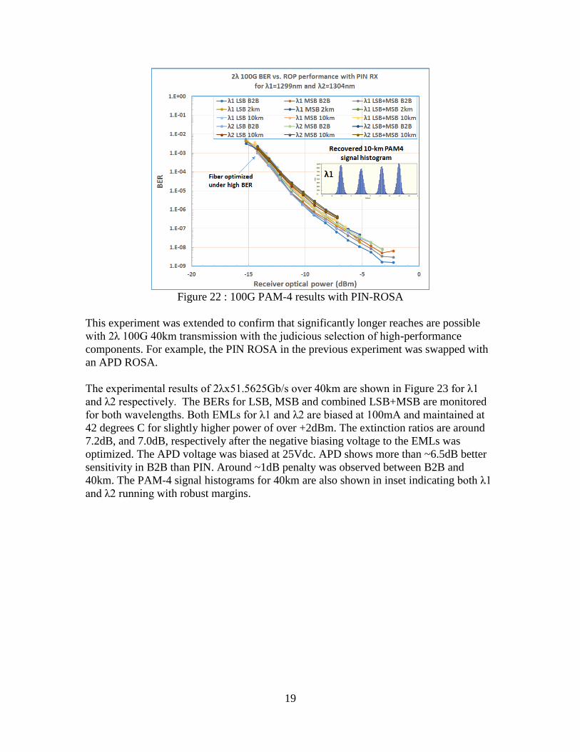
Figure 22 : 100G PAM-4 results with PIN-ROSA
This experiment was extended to confirm that significantly longer reaches are possible
with 2λ 100G 40km transmission with the judicious selection of high-performance
components. For example, the PIN ROSA in the previous experiment was swapped with
an APD ROSA.
The experimental results of 2λx51.5625Gb/s over 40km are shown in Figure 23 for λ1
and λ2 respectively. The BERs for LSB, MSB and combined LSB+MSB are monitored
for both wavelengths. Both EMLs for λ1 and λ2 are biased at 100mA and maintained at
42 degrees C for slightly higher power of over +2dBm. The extinction ratios are around
7.2dB, and 7.0dB, respectively after the negative biasing voltage to the EMLs was
optimized. The APD voltage was biased at 25Vdc. APD shows more than ~6.5dB better
sensitivity in B2B than PIN. Around ~1dB penalty was observed between B2B and
40km. The PAM-4 signal histograms for 40km are also shown in inset indicating both λ1
and λ2 running with robust margins.

20
Figure 23: 100G PAM-4 results with APD over 40Km SMF
3.3 100GBASE-KR4 compliant backplane within a Layer-3 Switch
3.3.1 Objective
An electrical backplane forms the backbone of a Layer-3 switch by providing
point-to-point connections between the line cards and switch/fabric cards. Current
100GbE deployments are typically built around 4x 25G NRZ serial links with combined
link comprising line-card, backplane and fabric card traces compliant to IEEE Std.
802.3bj 100GBASE-KR4.
Figure 24: Layer-3 Switch chassis
(Source: http://www.lightreading.com/document.asp?doc_id=25989)
As the front-panel capacity on the line cards scales upwards from 100G/port to 200G
and/or 400G/port, the backplane capacity would need to scale accordingly. But to run, for

21
example 50G/lane on existing IEEE Std. 802.3bj 100GBASE-KR4 compliant channels,
the insertion loss can approach 60dB+ for NRZ signaling posing a significant challenge
for Rx design while using PAM-4 signaling has the obvious benefits of keeping the
Nyquist the same for 25Gbps.
This section aims to demonstrate the technical feasibility of pushing 50G/lane using
PAM-4 over existing IEEE Std. 802.3bj 100GBASE-KR4 compliant backplane channels.
3.3.2 Lab Setup
The lab setup for backplane evaluation is based on a TE Connectivity STRADA Whisper
Backplane Test Kit shown in Figure 25. The experiments below focus on the longest 30”
trace on the backplane. Including the 5” traces on each of the paddle cards, the total trace
length is 40” (1 meter).
Figure 25 : The TE STRADA Whisper Backplane Evaluation System
A block diagram of the link setup build around this backplane is depicted in Figure 26
and the actual photograph of the bench is captured in Figure 27.
Figure 26 : Lab Setup Diagram for 100G PAM-4 Backplane Evaluation

22
Figure 27 : Lab Setup for 100G PAM-4 Backplane Evaluation
Similar to the setup in Section 3.1, a Viavi (formerly JDSU) ONT-603 Network Tester
generated the Ethernet traffic frames emulating a typical host with 100% utilization in the
MAC layer. The PAM-4 XCVR chip was configured to use the IEEE Std. 802.3bj
100GBASE-KR4 FEC and the FFE and DFE functions were enabled in the DSP. The
PAM-4 Tx output was set as 1Vppd and the FIR coefficients were optimized for this
channel utilizing SNR and eye-margin data from the Rx. The 100GbE traffic eventually
terminates back to the ONT-603 which continuously monitors for PHY, PCS and MAC
layer throughput and performance.
Figure 28: Insertion Loss (top) and Insertion Loss Deviation (bottom) of the backplane
kit and additional fixtures

23
The two PAM-4 “thru” backplane channels used were labelled [G14-G15] and [H11-
H12] set on the paddle cards. The insertion loss of the STRADA Whisper backplane 40”
[G14-G15] channel only is compared to the complete test system link which includes the
backplane kit and additional fixtures in Figure 28 which also shows the ILD. The other
[H11-H12] trace is designed to have very similar characteristics.
Additional PAM-4 Evaluation boards were connected to excite the crosstalk aggressors in
the STRADA Whisper Connector system. For the [G14-G15] victim, connector pairs
[F14-F15], [G11-G12], [G17-G18] and [H14-H15] were used as Near-End Crosstalk
(NEXT) aggressors. And connector pairs [F11-F12], [F17-F18], [H11-H12] and [H17-
H18] were used as Far-End Crosstalk (FEXT) aggressors.
The ICN (Integrated Crosstalk Noise) computed using IEEE COM methods was
approximately 2mV for the setup. It is to be noted that this calculation is specifically for
the backplane kit and does not include the additional lab fixtures used in this experiment.
Figure 29: TE STRADA Whisper 40” Crosstalk Profile, Source: Tyco Electronics
Furthermore, the crosstalk transmitters were clocked asynchronously to the victim
channels to sweep over possible worst-case alignments, as would be representative in a
real system. In addition, all NEXT crosstalk transmitters were setup to be 1V ppd
amplitude with no TX FIR settings applied. This setup condition is worse than typically
expected, since a real-life system will have some additional crosstalk filtering due to the
application of TX FIR settings for all applicable transmitters connected to a typical
40inch channel.
3.3.3 Test Results
The PAM-4 receiver measured SNR at the slicer and BER before FEC on both the 50G
lanes are shown in Table 3. The theoretical SNR and pre-FEC BER limits are extracted
from numerical analysis as illustrated in Figure 13.

24
Table 3: Link performance data on TE STRADA Whisper backplane
The Slicer Histogram capture and the post-equalized eye diagram are shown in Figure 30
and Figure 31 respectively.
Figure 30: TE STRADA Whisper 40" backplane PAM-4 Slicer Histogram
Figure 31: TE STRADA Whisper 40" backplane PAM-4 eye at Rx Slicer
Long-term gating tests included overnight runs where the setup was continuously
monitored for Bit and Frame Errors. There were none recorded with the setup running
error-free with BER<1E-15. The setup photograph in Figure 27 shows zero errors on all
layers with the backplane application as seen on the ONT-603 display.

25
The above experiment clearly demonstrates the feasibility of running 50G/lane PAM-4
modulation reliably for IEEE Std. 802.3bj 100GBASE-KR4 compliant backplane
channels.
4. Conclusions
With multiple contributions on PAM-4 technology in the IEEE and other industry MSAs
and with the IEEE 400Gbps taskforce agreeing to use PAM-4 for next-generation
electrical and optical interfaces, this paper demonstrates that not only does the technology
work, it can be productized and is indeed the right way forward for 50/100/200/400GbE
future deployments in datacenters.
Acknowledgements
We thank Megha Shanbhag and TE Connectivity Solutions for the 3m QSFP28 DAC
Cable and the STRADA Whisper Backplane kits used in this study.
We thank Keysight, Discovery Semiconductors, NeoPhotonics, Avago, Oplink, and SEDI
for various optical components and specialized test equipment that were provided for this
evaluation at different times.
References
[1] Google, Inc, "Jupiter Rising: A Decade of Clos Topologies," 2015. [Online].
Available: http://conferences.sigcomm.org/sigcomm/2015/pdf/papers/p183.pdf.
[2] B. Benson and A. Akella, "Network Traffic Characteristics of Data Centers in the
Wild," in 10th ACM SIGCOMM conference on Internet, 2010.
[3] B. Booth and T. Issenhuth, "Objectives to Support Cloud Scale Data Center Design,"
in IEEE 802.3 400Gb/s Ethernet Study Group, Dallas, TX, 2013.
[4] S. Bhoja, "Precoding proposal for PAM4 modulation," in IEEE P802.3bj Task Force,
2011.
[5] K. H. Mueller and M. S. Muller, "Timing Recovery in Digital Synchronous Data
Receivers," IEEE Transactions on Communications, Vols. COM-24, pp. 516-531,
1976.
[6] "CWDM4 MSA Group," [Online]. Available: http://www.cwdm4-msa.org.php53-
12.ord1-1.websitetestlink.com/.
[7] "IEEE P802.3bs 400Gb/s Ethernet Task Force," 2015. [Online]. Available:
http://www.ieee802.org/3/bs/public.


![DesignCon 2014 - SiSoft...1 DesignCon 2014 How Design of Experiments Saved my CEI VSR 28G Design Richard Allred, SiSoft [rallred@sisoft.com] Barry Katz, SiSoft Ishwar Hosagrahar, Inphi](https://img.pdfslide.us/doc/110x75/5f19284848bb9016ff191954/designcon-2014-sisoft-1-designcon-2014-how-design-of-experiments-saved-my.jpg)