Embed Size (px)
Citation preview

Design and CAD Methodologies for Low Power Gate-levelMonolithic 3D ICs
Shreepad Panth†, Kambiz Samadi§, Yang Du§, and Sung Kyu Lim†
†School of ECE, Georgia Institute of Technology, Atlanta, GA§Qualcomm Research, San Diego, CA
spanth,[email protected]
ABSTRACT
In a gate-level monolithic 3D IC (M3D), all the transistors in a sin-gle logic gate occupy the same tier, and gates in different tiers areconnected using nano-scale monolithic inter-tier vias. This designstyle has the benefit of the superior power-performance quality of-fered by flat implementations (unlike block-level M3D), and zerototal silicon area overhead compared to 2D (unlike transistor-levelM3D). In this paper we develop, for the first time, a complete RTL-to-GDSII design flow for gate-level M3D. Our tool flow is basedon commercial tools built for 2D ICs and enhanced with our 3D-specific methodologies. We use this flow along with a 28nm PDKto build layouts for the OpenSPARC T2 core. Our simulationsshow that at the same performance, gate-level M3D offers 16%total power reduction with 0% area overhead compared to com-mercial quality 2D IC designs.
Categories and Subject Descriptors
B.7.2 [Integrated Circuits]: Design Aids—Placement and routing
Keywords
Monolithic 3D; Timing Closure
1. INTRODUCTIONMonolithic 3D ICs (M3D) are an emerging technology that of-
fers orders of magnitude higher integration density than other 3Dintegration technologies such as through-silicon-via (TSV), siliconinterposer, etc, thanks to its nano-scale monolithic inter-tier vias(MIVs) [1]. There are three design styles possible for monolithic3D ICs: transistor-level, gate-level, and block-level. In transistor-level monolithic 3D ICs [2, 5], the PMOS and NMOS within eachstandard cell is split into different tiers, andMIVs are used for intra-cell as well as inter-cell connections. This is the finest-grained in-tegration style, and has the advantage that the PMOS and NMOSfabrication process can be optimized separately. However, it re-quires redesign and re-characterization of the standard cells them-selves, which takes significant effort. Also, the standard cell foot-
This work is supported by Qualcomm Research.
Permission to make digital or hard copies of all or part of this work for personal or
classroom use is granted without fee provided that copies are not made or distributed
for profit or commercial advantage and that copies bear this notice and the full cita-
tion on the first page. Copyrights for components of this work owned by others than
ACMmust be honored. Abstracting with credit is permitted. To copy otherwise, or re-
publish, to post on servers or to redistribute to lists, requires prior specific permission
and/or a fee. Request permissions from [email protected].
ISLPED’14, August 11–13, 2014, La Jolla, CA, USA
Copyright 2014 ACM 978-1-4503-2975-0/14/08 ...$15.00.
http://dx.doi.org/10.1145/2627369.2627642.
print does not reduce by 50% in 3D due to the mismatch in thePMOS and NMOS sizes. This leads to an increase in total siliconarea and cost.
The next design style is gate-level monolithic 3D ICs, where ex-isting standard cells and memory can simply be reused. Gates areplaced onto multiple tiers, and MIVs are used to connect them to-gether. The authors of [2] provided a rudimentary design flow thatis not capable of handling any hard macros such as memory, andtherefore cannot be applied to real designs. The last design style isblock-level monolithic 3D ICs, where functional blocks are floor-planned onto different tiers [7]. This style has the benefit of IPreuse, but does not fully take advantage of the fine-grained natureof MIVs. Since the blocks are implemented in 2D, the power ben-efit of this style is limited.
This paper focuses on gate-level monolithic 3D ICs because theyoffer the reuse of existing standard cells and memory, zero totalsilicon area overhead (unlike transistor-level), and a sufficientlyhigh integration density to obtain significant power benefits (un-like block-level). In addition, we focus only on the two-tier case,as it requires only one silicon attachment step. This paper pro-poses, for the first time, a CAD methodology that is capable of tak-ing gate-level monolithic 3D IC designs all the way though place,route, clock-tree-synthesis, and timing optimization. We use theOpenSPARC T2 [6] core as a case study, and demonstrate thatmonolithic 3D ICs offer significant power benefits compared tocommercial-quality 2D IC designs.
We demonstrate that using multiple MIVs per signal net canhelp reduce the total wirelength by 10.03%, giving us a 4.53% netpower reduction, which in turn translates into 2.66% total powersavings. Next, we present a CTS methodology, that when com-pared with existing techniques, reduces the clock wirelength andbuffer count by 21.91% and 21.56% respectively. This leads to aclock power reduction of 29.82%. When compared to a 2D clocktree, our CTS method enables monolithic 3D to have 23.20% lessclock power. All these techniques enable us to achieve 15.57% to-tal power reduction when compared to commercial-grade 2D ICs.Finally, we demonstrate that the power benefit of M3D carries overeven when using dual-Vt libraries, and the total power savings risesto 16.08%.
2. DIE STACKING TECHNOLOGIESWe show the various design styles for monolithic 3D ICs in Fig-
ure 1(a). As seen from this figure, transistor-level integration is themost fine-grained technique. However, since MIVs are requiredwith each cell, there is an increase in the total cell area (as seenin the INV cell). In addition, each cell will need to be redesignedfrom scratch. In gate-level monolithic 3D ICs, we observe thatthere is no area overhead for each cell. We also observe that since

(a) Monolithic 3D ICs
NAND INV
NAND
TSV
μ-bump
(b) Gate-level TSV-based 3D IC
NAND INVF2F via
(c) Gate-level face-to-face 3D IC
ILD
NOR INV NORMIV
Transistor-level
INV NAND
Block-level
Block
Block
Gate-level
Figure 1: Various design styles available for different die stack-
ing technologies.
MIVs can be placed anywhere in between cells, a sufficiently highintegration density can be obtained, which will lead to significantpower savings. Lastly, we observe that in block-level integration,since each block is the same in 2D and 3D, the potential powerbenefit is limited.Out of the three styles considered, gate-level offers the greatest
balance between integration density and reuse of existing libraries.Therefore, we focus on gate-level integration in this paper. Forgate-level designs, we also show diagrams for TSV-based 3D ICsin Figure 1(b) and face-to-face 3D ICs in Figure 1(c). We clearlysee that in TSV-based 3D ICs, the via size is so large that the powerbenefit is limited. However, face-to-face 3D ICs offer only slightlylarger via sizes than monolithic 3D, and can also be consideredfine-grained. Therefore, we also include results for gate-level face-to-face 3D ICs in this paper.
3. CAD METHODOLOGYThis section presents our sign-off CAD methodology for mono-
lithic 3D ICs. This methodology is based on the fact that the z-dimension is negligible in monolithic 3D ICs (only a few µm),which enables us to utilize commercial 2D IC tools to performplace and route for M3D.
3.1 Overall MethodologyConsider a true 3D analytical placer that solves equations in
the x,y, and z dimensions. Since we consider only the rectilinearhalf-perimeter wirelength (HPWL), each axis is independent of theother, and is therefore solved independently. Now, since the z di-mension is so small (and discrete), all z solutions for a given x andy solution will have more or less the same HPWL. This impliesthat a 2D placer can be used to first find the x and y solutions, andthe z location can be determined as a post-process. Note that thisentire process is contingent on the 2D placer being able to place allthe gates in a monolithic 3D IC footprint, which is half the foot-print area of a 2D IC. This requires several techniques to utilize the
Technology Scaling Memory Scaling
Memory Placement
Memory Flattening
Shrunk 2D Place & Route
Tier Partitioning
Initial Timing Analysis
Tier-by-tier Route
3D Timing & Power Analysis
Cadence Encounter
Synopsys PrimeTime
Custom Script
Figure 2: The overall CADmethodology flow used in this paper.
commercial 2D IC tool. In addition, memory complicates the issue,as they are pre-placed in both tiers, and this somehow needs to befed into the commercial tool.
The overall design flow is shown in Figure 2. First, in order toutilize the 2D tool to handle all the standard cells in a reduced foot-print, several technology files are scaled, and this process will bedescribed in detail in Subsection 3.2. Next, memory handling re-quires several steps such as memory scaling, memory placementand memory flattening, which will be described in detail in Sub-section 3.3. Once this is done, the commercial 2D engine (CadenceEncounter) can be run on this “shrunk 2D” design (described inSubsection 3.4). This result is then split into multiple tiers to ob-tain a DRC-clean sign-off design as described in Subsection 3.5,and finally timing and power analysis is performed as described inSubsection 3.6.
3.2 Scaling Technology FilesThe goal of this step is twofold. We need to utilize the com-
mercial 2D tool into placing all the gates in half the footprint area,and we also need to make sure that the wire RC information thatthe tool sees accurately reflects what will be present in the final 3Ddesign. Note that this subsection assumes a gate-only design, andhandling memory will be introduced in Subsection 3.3.
Placing all the gates into half the area can be achieved by shrink-ing the area of each standard cell by 50%. We scale the width,height and the location of all the pins within the cell by 1/
√
2
(0.707). In addition, the chip width and height are scaled by 0.707to reduce the 2D footprint area by half. This will also be the foot-print of each tier in the final M3D design. Note that since the x andy axis equations in an analytical placer are linear, scaling all thedimensions by 0.707 will simply make the cell locations 0.707 ofwhat they used to be in the 2D placement solution. This leads to atheoretical HPWL improvement of 29.3%.
Next, in order to make the routing in the shrunk 2D accuratelyrepresent the routing in monolithic 3D, we shrink both the metalwidth and pitch of each metal layer by 0.707. Since the chip widthand height are also shrunk by the same amount, the total routingtrack length does not change between 2D and shrunk 2D. The totaltrack length will also be the same once we go to 3D; hence, thismethod gives a good estimate of wire length. Note that we do not
change the wire RC per unit length, even though the wire widthis smaller. Therefore, the extracted RC values from the tool doesnot reflect the geometry of shrunk 2D, but that of a M3D wire ofequivalent length using the original metal geometries.
3.3 Handling Memory MacrosWhile standard cells can be handled by shrinking their footprint,
this is not the case for memory. This is because standard cells canbe moved by the placer, while memory is pre-placed. Since nostandard cell can be placed in the location where a memory is pre-placed, simply shrinking the memory is not an option. We utilizethe fact that a pre-placed memory can be thought of as a combina-
New
Footprint
Pins outside
footprint
(a) (b)
Memory Pins
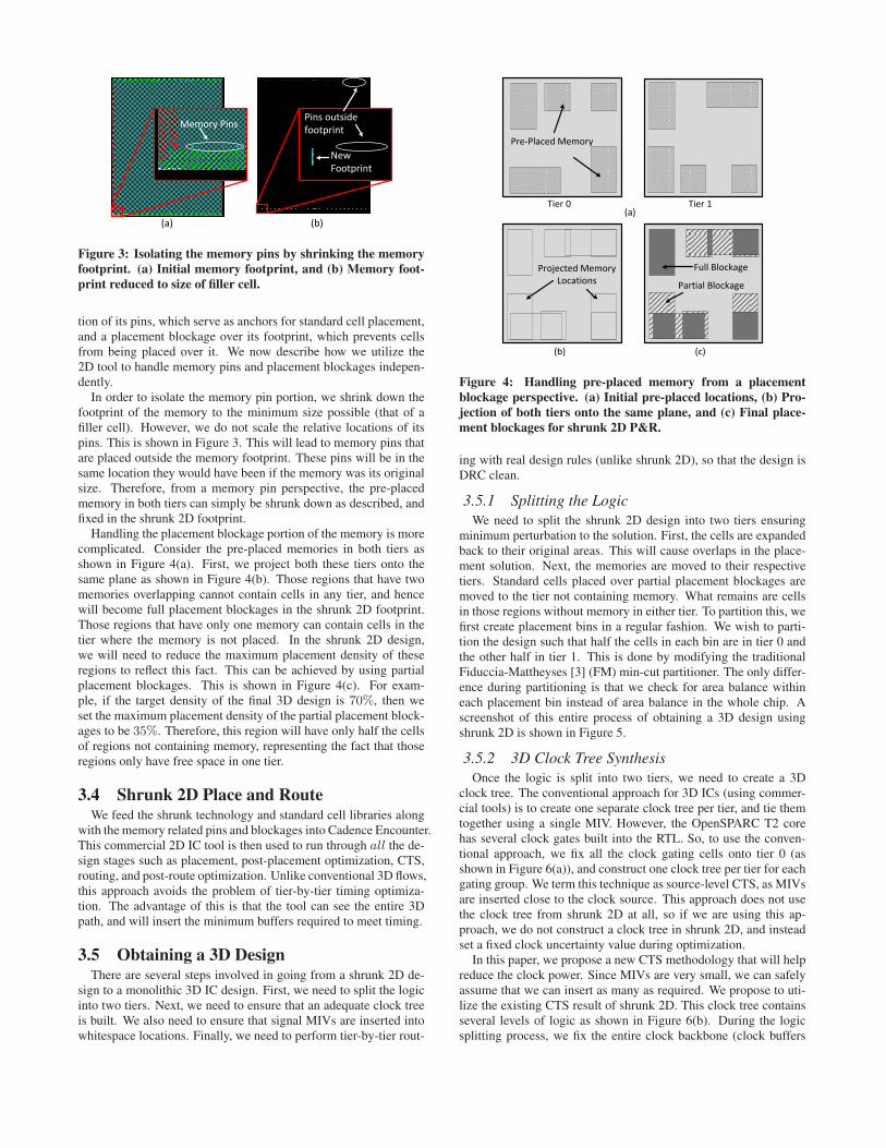
Figure 3: Isolating the memory pins by shrinking the memory
footprint. (a) Initial memory footprint, and (b) Memory foot-
print reduced to size of filler cell.
tion of its pins, which serve as anchors for standard cell placement,and a placement blockage over its footprint, which prevents cellsfrom being placed over it. We now describe how we utilize the2D tool to handle memory pins and placement blockages indepen-dently.In order to isolate the memory pin portion, we shrink down the
footprint of the memory to the minimum size possible (that of afiller cell). However, we do not scale the relative locations of itspins. This is shown in Figure 3. This will lead to memory pins thatare placed outside the memory footprint. These pins will be in thesame location they would have been if the memory was its originalsize. Therefore, from a memory pin perspective, the pre-placedmemory in both tiers can simply be shrunk down as described, andfixed in the shrunk 2D footprint.Handling the placement blockage portion of the memory is more
complicated. Consider the pre-placed memories in both tiers asshown in Figure 4(a). First, we project both these tiers onto thesame plane as shown in Figure 4(b). Those regions that have twomemories overlapping cannot contain cells in any tier, and hencewill become full placement blockages in the shrunk 2D footprint.Those regions that have only one memory can contain cells in thetier where the memory is not placed. In the shrunk 2D design,we will need to reduce the maximum placement density of theseregions to reflect this fact. This can be achieved by using partialplacement blockages. This is shown in Figure 4(c). For exam-ple, if the target density of the final 3D design is 70%, then weset the maximum placement density of the partial placement block-ages to be 35%. Therefore, this region will have only half the cellsof regions not containing memory, representing the fact that thoseregions only have free space in one tier.
3.4 Shrunk 2D Place and RouteWe feed the shrunk technology and standard cell libraries along
with the memory related pins and blockages into Cadence Encounter.This commercial 2D IC tool is then used to run through all the de-sign stages such as placement, post-placement optimization, CTS,routing, and post-route optimization. Unlike conventional 3D flows,this approach avoids the problem of tier-by-tier timing optimiza-tion. The advantage of this is that the tool can see the entire 3Dpath, and will insert the minimum buffers required to meet timing.
3.5 Obtaining a 3D DesignThere are several steps involved in going from a shrunk 2D de-
sign to a monolithic 3D IC design. First, we need to split the logicinto two tiers. Next, we need to ensure that an adequate clock treeis built. We also need to ensure that signal MIVs are inserted intowhitespace locations. Finally, we need to perform tier-by-tier rout-
Partial Blockage
Pre-Placed Memory
Projected Memory
Locations
(a)
(b) (c)
Tier 0 Tier 1
Full Blockage
Figure 4: Handling pre-placed memory from a placement
blockage perspective. (a) Initial pre-placed locations, (b) Pro-
jection of both tiers onto the same plane, and (c) Final place-
ment blockages for shrunk 2D P&R.
ing with real design rules (unlike shrunk 2D), so that the design isDRC clean.
3.5.1 Splitting the Logic
We need to split the shrunk 2D design into two tiers ensuringminimum perturbation to the solution. First, the cells are expandedback to their original areas. This will cause overlaps in the place-ment solution. Next, the memories are moved to their respectivetiers. Standard cells placed over partial placement blockages aremoved to the tier not containing memory. What remains are cellsin those regions without memory in either tier. To partition this, wefirst create placement bins in a regular fashion. We wish to parti-tion the design such that half the cells in each bin are in tier 0 andthe other half in tier 1. This is done by modifying the traditionalFiduccia-Mattheyses [3] (FM) min-cut partitioner. The only differ-ence during partitioning is that we check for area balance withineach placement bin instead of area balance in the whole chip. Ascreenshot of this entire process of obtaining a 3D design usingshrunk 2D is shown in Figure 5.
3.5.2 3D Clock Tree Synthesis
Once the logic is split into two tiers, we need to create a 3Dclock tree. The conventional approach for 3D ICs (using commer-cial tools) is to create one separate clock tree per tier, and tie themtogether using a single MIV. However, the OpenSPARC T2 corehas several clock gates built into the RTL. So, to use the conven-tional approach, we fix all the clock gating cells onto tier 0 (asshown in Figure 6(a)), and construct one clock tree per tier for eachgating group. We term this technique as source-level CTS, as MIVsare inserted close to the clock source. This approach does not usethe clock tree from shrunk 2D at all, so if we are using this ap-proach, we do not construct a clock tree in shrunk 2D, and insteadset a fixed clock uncertainty value during optimization.
In this paper, we propose a new CTS methodology that will helpreduce the clock power. Since MIVs are very small, we can safelyassume that we can insert as many as required. We propose to uti-lize the existing CTS result of shrunk 2D. This clock tree containsseveral levels of logic as shown in Figure 6(b). During the logicsplitting process, we fix the entire clock backbone (clock buffers

Tier 0
Pre-placed Memory
Par!al Blockage
Reduced Placement Density
over Par!al Blockages
Full Blockage
Memory Pins
Tier 1
Memory Fla"ening Shrunk 2D P&R
Tier Par!!oning
Figure 5: Pre-placed memory is flattened to get a shrunk 2D footprint, on which 2D P&R is performed. This is then partitioned to
get a monolithic 3D solution.
Clock BufferClock gate
Flip-flop
Tier 0
Tier 0 Tier 1 Tier 0 Tier 1
Tier 0
3D Net
3D Net(a) (b)
Figure 6: Two different types of 3D CTS possible (a) One clock
tree per tier for each gating group (source-level), and (b) The
entire backbone is fixed onto tier 0 (leaf-level).
and clock gates) onto tier 0. Only the leaf-level flip-flops are freeto be partitioned to maintain area balance. Therefore, MIVs willbe inserted following all leaf clock buffers that drive flip-flops inboth tiers. We determine these clock MIV locations using an ap-proach similar to what will be described in Subsection 3.5.3, andthen once the tiers are split, we re-route the leaf-level clock nets.This approach is termed leaf-level CTS, and an example of this ap-proach for the OpenSPARC T2 core is shown in Figure 7.
3.5.3 Signal MIV Insertion
We utilize a 2D router that is capable of routing to pins on mul-tiple metal layers to perform MIV insertion for us. First, all themetal layers in the technology LEF are duplicated to yield a new3D LEF with twice the number of metal layers. Next, for each cellin the LEF file, we define two flavors – one for each tier. The onlydifference between the two flavors is that their pins are mappedonto different metal layers depending on tier. Next, each cell in the3D space is mapped to its appropriate flavour, and forced onto thesame placement layer. Note that this will lead to cell overlap in theplacement layer, but there will be no overlap in the routing layers.We also place routing blockages in the via layer between the twotiers, to prevent MIVs being placed over cells. This entire structureis then fed into Cadence Encounter. Once routed, we trace the rout-ing topology to extract the MIV locations, and generate separateverilog/DEF files for each tier.Note that for certain nets, the router is bound to insert multiple
MIVs. Since existing 3D tool flows use tier-by-tier optimization,
(a)
Clock MIV
Leaf clock net
Flip-Flop
Clock backbone
Leaf
buffer
(b)
Figure 7: Our proposed CTS methodology (a) The clock back-
bone in tier 0, and (b) Zoom-in shot of leaf-level flip-flops in
both tiers connected to a leaf clock buffer in tier 0.
timing constraints need to be derived for each tier. In each tier,MIVs are defined as I/O ports, and the timing constraints are cap-tured as input/output delays. However, if a single net contains mul-tiple MIVs, then it becomes very difficult to capture multiple in-put/output delays on a single net, as such conditions do not arise in2D ICs (which current tools are designed for). Therefore, multipleMIV insertion is converted to single MIV insertion by picking thebest MIV (in terms of HPWL) from those inserted, and re-routingthe net. This could potentially increase the wirelength, but is un-avoidable for conventional 3D flows. In our flow, since the opti-mization is performed in the shrunk 2D design and not tier-by-tier,we can use multiple MIV insertion, which will reduce wirelengthand give us a power benefit. Routing topologies for single and mul-tiple MIV insertion for a given net are shown in Figure 8.
Note that the approach proposed here is not limited to monolithic3D ICs, and can also be applied to other fine-grained 3D integra-tion technologies such as face-to-face (F2F) integration. This canbe achieved by simply changing the order of the metal layers in thegenerated 3D technology LEF file, and not adding a routing block-age over cells, thereby allowing F2F vias to be placed over cells.This is because F2F vias occupy the top metal layer only, and do notrequire placement space. Sample MIV and F2F vias after insertionare shown in Figure 9.

Tier0 Mul ple MIVs
Single 3D connec on
(a)
Tier1
Tier0
Tier1
(b)
Figure 8: Two types of MIV insertion for a 3D net (a) Single,
(b) Multiple
(a) (b)
MIV
F2F
Figure 9: (a) Monolithic 3D integration, and (b) Face-to-face
3D integration. MIVs are limited to whitespace, while F2F vias
are not.
3.6 Timing and Power AnalysisOnce the MIV/F2F locations are determined, each tier is first
trial routed and estimates of parasitics for each tier are dumped.The netlist for each tier, along with its parasitics is then fed intoSynopsys PrimeTime. In addition, a top-level netlist and parasiticfile is created that contains the MIV/F2F connectivity and para-sitics. With all this information, an initial timing analysis is per-formed to derive timing constraints for each tier. With these timingconstraints, we go back to each tier, and run timing-driven rout-ing. The real sign-off parasitics for each tier are then fed back intoPrimeTime to get the final timing and statistical power simulationnumbers.
4. POWER BENEFIT STUDYWe choose the OpenSPARC T2 core as a case study, implement
it in a 28nm technology library and explore the power benefit thatmonolithic 3D ICs offer when compared to a commercial qualitysign-off 2D design. All the numbers presented in this section arefor timing closed designs, with a frequency of 1Ghz. This is themaximum frequency that we could design the 2D version using ahigh-effort timing-driven flow in Cadence Encounter. The footprintarea of the monolithic 3D IC design is exactly half that of the 2Ddesign, and therefore, all 3D designs presented here have zero totalsilicon area overhead when compared to 2D.The MIV diameter is assumed to be 100nm, and its resistance
and capacitance are assumed to be 2Ω and 0.1fF respectively. Wealso provide comparisons with face-to-face integration and the F2Fvia diameter, resistance and capacitance are assumed to be 500nm,0.5Ω and 0.2fF respectively. All required scripts are implementedin C/C++, Python and Tcl.
Table 1: Comparison of single vs. multiple MIV/F2F insertion.
Power values are reported in mW, and wirelength in meter.Monolithic 3D Face-to-face
Single Multiple Diff(%) Single Multiple Diff(%)
Total WL 15.61 14.29 -8.43 15.44 13.89 -10.05#MIV/F2F 106k 235k +120.44 106k 202k +89.72
Total Pwr 534.10 522.10 -2.25 538.30 524.00 -2.66
Cell Pwr 126.90 126.10 -0.63 127.30 126.40 -0.71Net Pwr 293.90 282.70 -3.81 297.80 284.30 -4.53Lkg Pwr 113.30 113.30 0.00 113.30 113.30 0.00
Table 2: Comparison of two different types of 3D CTS. Power
values are reported in mW, and wirelength in meter.Monolithic 3D Face-to-face
Source- Leaf- Diff Source- Leaf- Difflevel level (%) level level (%)
#MIV/F2F 871 11,376 +1.2k 871 11,376 +1.2kSkew (ps) 197.42 103.00 -47.83 172.90 117.07 -32.29
Clock Pwr 68.40 48.00 -29.82 69.00 48.50 -29.71
Tier0 WL 0.55 0.62 +11.89 0.53 0.62 +16.61Tier1 WL 0.48 0.19 -60.50 0.48 0.17 -64.85Total WL 1.03 0.80 -21.67 1.01 0.79 -21.91
#Tier0 Buf 14,610 21,687 +48.44 14,958 21,687 +44.99#Tier1 Buf 12,444 0 -100 12,691 0 -100#Total Buf 27,054 21,687 -19.84 27,649 21,687 -21.56
4.1 Single vs. Multiple MIV InsertionWe first discuss the power benefit offered by using multipleMIVs
(or F2F vias) for each 3D net. A summary of results for both sin-gle and multiple MIV insertion is tabulated in Table 1. From thistable, we observe that using multiple vias offers 8.4% and 10.04%wirelength reduction for M3D and F2F respectively. We also notethat the number of 3D vias double. This means that each net is, onaverage, using approximately two MIV/F2F vias. This wirelengthreduction does not reduce leakage power, but it does reduce somecell power. The biggest reduction is in net power, which reducesby 3.81% and 4.53% for M3D and F2F, which translates to 2.25%and 2.66% total power reduction, respectively.
4.2 CTS: Source-level vs. Leaf-levelIn this section, we discuss the power benefit that our proposed
CTS methodology (leaf-level) offers over existing 3D techniques(source-level). A summary of results is tabulated in Table 2. Fromthis table, we first observe that leaf-level CTS offers huge reduc-tions in clock skew, as well as a 29.82% reduction in the clocktree power. There are 871 clock-gating related cells in the design,which is why source-level CTS uses that number of MIV/F2F vias.We observe that leaf-level uses far more 3D vias, which helps re-duce the clock power.
These power reduction numbers can be explained on the basisof per-tier wirelength and buffer count. We observe that leaf-leveluses far more buffers and has a longerWL on tier 0, which is the tierwith the clock-backbone. On the other hand, the number of buffersis zero in tier 1 and theWL is much smaller. In comparison, source-level has a more balanced clock WL and buffer count between thetiers, but this comes at the cost of an increase in the total clock WLand buffer count.
4.3 Overall Comparisons: 2D vs. 3DUsing the techniques that give us the best power reduction (i.e.
multiple MIV insertion and leaf-level CTS), we now make a com-parison of M3D and F2F with a 2D IC designed using CadenceEncounter. A summary of results is tabulated in Table 3. From this

Table 3: Overall comparisons between 2D and different 3D implementation stylesEncounter 2D Shrunk 2D Monolithic 3D Face-to-face
Total WL(m) 17.96 13.10 ( -27.05% ) 14.29 ( -20.40% ) 13.89 ( -22.65% )# MIV/F2F - - 235,394 235,394# Buffers 164,917 128,098 ( -22.33% ) 128,098 ( -22.33% ) 128,098 ( -22.33% )
#Total Gates 458,824 421,959 ( -8.03% ) 421,959 ( -8.03% ) 421,959 ( -8.03% )
Total Power (mW) 618.40 514.40 ( -16.82% ) 522.10 ( -15.57% ) 524.00 ( -15.27% )
Cell Power (mW) 135.60 126.80 ( -6.49% ) 126.10 ( -7.01% ) 126.40 ( -6.78% )Net Power (mW) 356.30 274.30 ( -23.01% ) 282.70 ( -20.66% ) 284.30 ( -20.21% )
Leakage Power (mW) 126.50 113.30 ( -10.43% ) 113.30 ( -10.43% ) 113.30 ( -10.43% )
Memory Power (mW) 49.00 45.10 ( -7.96% ) 45.10 ( -7.96% ) 45.00 ( -8.16% )Combinational Power (mW) 385.10 300.00 ( -22.10% ) 305.30 ( -20.72% ) 306.80 ( -20.33% )Clock Tree Power (mW) 62.50 46.90 ( -24.96% ) 48.00 ( -23.20% ) 48.50 ( -22.40% )FF Clock Pin Power (mW) 9.70 9.90 ( +2.06% ) 9.60 ( -1.03% ) 9.70 ( 0.00% )
Register Power (mW) 112.10 112.50 ( +0.36% ) 114.00 ( +1.69% ) 114.00 ( +1.69% )
table, we first observe that shrunk 2D reduces the wirelength by27.05% compared to 2D. This is very close to the 29.3% HPWLbound predicted in Section 3. The improvement number goes downfor both M3D and F2F, which is to be expected. In addition, M3Dhas slightly higher WL compared to F2F because the MIVs are lim-ited to whitespace, while F2F vias are not. Next, we observe thatthe 3D implementations reduce the buffer count by 22.3%, whichtranslates to a 8.03% reduction in total gate count. Since MIV andF2F designs are obtained by simply splitting the shrunk 2D design,all three have the same gate counts. The reduced wirelength andgate count lead to a total power reduction of 15.57% and 15.27%for M3D and F2F respectively. We observe that F2F has a higherpower consumption than M3D even though it has lower WL, whichis due to increased parasitics of F2F vias. Also, both M3D and F2Fpower numbers are quite close to the shrunk 2D numbers, whichshows that the shrunk 2D design is a very good estimate of M3Dand other fine-grained 3D technologies.We first divide the total power into cell, net, and leakage power.
From the table, we observe that the cell power reduces at a numberroughly equal to the total gate count reduction. The net power re-duces roughly proportional to wirelength, and finally, the leakagereduction is slightly larger than cell count reduction due to smallerbuffer sizes. We can also split up the total power by lumping theinternal, net and leakage power of certain classes of gates/memorytogether. This is also tabulated in Table 3. We observe that the flip-flop clock pin power and register power are virtually unchanged in3D. The biggest savings in power come from combinational logic(20.72% savings), and from the clock tree (23.20% savings). Wealso observe some memory power savings due to reduction in theoutput net length that the memory drives.
4.4 Impact of Dual-Vt GatesAll the results discussed so far have used only the regular Vt
standard cell library for both 2D and 3D designs. However, it isknown that converting cells on non-critical paths to a high Vt flavorcan help reduce leakage power. In this section, we evaluate dual Vt
designs (DVT), and investigate whether the power benefit of M3Dcarries over from the single Vt designs (SVT).For both 2D and 3D (shrunk 2D), we initially use Encounter to
perform leakage optimization during the P&R flow. We also per-form leakage optimizations in PrimeTime using a script similar to[4], and tabulate the results in Table 4. From this table, we observethat M3D designs reduce the total power of 2D designs by 16.08%.This is a slightly better improvement number than the SVT casealone. This is due to the fact that there are more paths that becomenon-critical in 3D. We also observe that the F2F improvement num-bers are better than the SVT case. Therefore, the 3D power benefitnot only carries over to dual-Vt designs, it actually improves.
Table 4: Dual-Vt comparisons between 2D and different 3D
implementation styles. Power is in mW.Enc. 2D Monolithic 3D Face-to-face
Total WL(m) 17.94 14.29 ( -20.33% ) 13.89 ( -22.59% )#MIV/F2F - 235,394 202,593
Total Pwr 572.10 480.10 ( -16.08% ) 482.20 ( -15.71% )
Cell Pwr 131.80 123.00 ( -6.68% ) 123.30 ( -6.45% )Net Pwr 356.60 282.70 ( -20.72% ) 284.30 ( -20.27% )Leak. Pwr 83.60 74.40 ( -11.00% ) 74.60 ( -10.77% )
Mem. Pwr 48.80 45.10 ( -7.58% ) 45.00 ( -7.79% )Comb. Pwr 361.60 283.00 ( -21.74% ) 284.30 ( -21.38% )Clk Tree Pwr 62.50 48.00 ( -23.20% ) 48.50 ( -22.40% )FF Clk Pin Pwr 9.10 9.20 ( +1.10% ) 9.20 ( +1.10% )
Reg. Pwr 90.00 94.90 ( +5.44% ) 94.80 ( +5.33% )
5. CONCLUSIONIn this work, for the first time, we have demonstrated a CAD
methodology that is capable of taking gate-level monolithic 3DIC designs all the way though place, route, CTS, and timing op-timization. We have used the OpenSPARC T2 core as a case study,and demonstrated that monolithic 3D ICs offer significant powerbenefits when compared to commercial-quality 2D ICs. We havedemonstrated several low-power techniques such as multiple MIVinsertion and a leaf-level CTS methodology. All these techniquesenable us to achieve 15.57% total power reduction when comparedto commercial-grade 2D ICs. In addition, we demonstrate thatthe power benefit of M3D carries over even when using dual-Vt
libraries, and we can achieve a total power reduction of 16.08%.
6. REFERENCES
[1] P. Batude et al. Advances in 3D CMOS Sequential Integration. InProc. IEEE Int. Electron Devices Meeting, 2009.
[2] S. Bobba et al. CELONCEL: Effective design technique for 3-Dmonolithic integration targeting high performance integrated circuits.In Proc. Asia and South Pacific Design Automation Conf., 2011.
[3] C. M. Fiduccia and R. M. Mattheyses. A linear-time heuristic forimproving network partitions. In Proc. ACM Design Automation
Conf., 1982.
[4] P. Gupta, A. Kahng, P. Sharma, and D. Sylvester. Gate-length biasingfor runtime-leakage control. IEEE Trans. on Computer-Aided Design
of Integrated Circuits and Systems, 2006.
[5] Y.-J. Lee, D. Limbrick, and S. K. Lim. Power Benefit Study forUltra-High Density Transistor-Level Monolithic 3D ICs. In Proc.ACM Design Automation Conf., 2013.
[6] Oracle. OpenSPARC T2.
[7] S. Panth, K. Samadi, Y. Du, and S. K. Lim. High-Density Integrationof Functional Modules Using Monolithic 3D-IC Technology. In Proc.Asia and South Pacific Design Automation Conf., 2013.