Embed Size (px)
Citation preview

Design Techniques for EMC Part 2 - Cables andConnectors (first half of part 2)By Eur Ing Keith Armstrong C.Eng MIEE MIEEE, Cherry Clough Consultants
This is the second in a series of six articles on basic good-practice electromagnetic compatibility (EMC)techniques in electronic design, to be published during 2006. It is intended for designers of electronicmodules, products and equipment, but to avoid having to write modules/products/equipment throughout -everything that is sold as the result of a design process will be called a ’product’ here.
This series is an update of the series first published in the UK EMC Journal in 1999 [1], and includesbasic good EMC practices relevant for electronic, PCB and mechanical designers in all applications areas(household, commercial, entertainment, industrial, medical and healthcare, automotive, railway, marine,aerospace, military, etc.). Safety risks caused by electromagnetic interference (EMI) are not covered here;see [2] for more on this issue.
These articles deal with the practical issues of what EMC techniques should generally be used and howthey should generally be applied. Why they are needed or why they work is not covered (or, at least, notcovered in any theoretical depth) - but they are well understood academically and well proven overdecades of practice. A good understanding of the basics of EMC is a great benefit in helping to preventunder- or over-engineering, but goes beyond the scope of these articles.
The techniques covered in these six articles will be:1) Circuit design (digital, analogue, switch-mode, communications), and choosing components2) Cables and connectors3) Filters and transient suppressors4) Shielding5) PCB layout (including transmission lines)6) ESD, surge, electromechanical devices, power factor correction, voltage fluctuations, supply dips anddropouts
Many textbooks and articles have been written about all of the above topics, so this magazine articleformat can do no more than introduce the various issues and point to the most important of the basicgood-practice EMC design techniques. References are provided for further study and more in-depth EMCdesign techniques.
2. Part 2 - Cables and Connectors2.1 Introduction2.2 All conductors are ’accidental antennas’2.2.1 All conductors should use EMC design2.2.2 It might be cost-effective not to use conductors at all 2.2.3 Controlling the DM and CM current paths 2.2.4 Coaxial and twisted-send/return conductors2.2.5 Differential (’balanced’) interconnections2.3 Cable segregation

2.4 Unshielded interconnections 2.4.1 Unshielded wires and cables 2.4.2 Unshielded connectors 2.5 Earthing and grounding conductors 2.6 Shielded (screened) cables 2.6.1 How do we shield a wire or cable? 2.6.2 How shielded interconnections work2.6.3 Why coaxial cables aren’t very cost-effective for EMC 2.6.4 The ZT and Shielding Effectiveness (SE) of various types of cable2.6.5 More on designing shielded interconnections2.7 Transmission line interconnections 2.8 References: 2.9 Acknowledgements
2. Part 2 - Cables and Connectors
2.1 Introduction
This article concerns the EMC design of metal interconnections for analogue and digital signals, andpulse-width modulated (PWM), AC or DC power. These interconnections can be between differentcircuits inside a product, or between different products in a system or installation.
Until a few years ago, it could generally be assumed that, for most products, most of the EMC problems atradio frequencies (RF) concerned their external cables, because they were long enough to act asreasonably effective ’accidental antenna’ at the frequencies being employed by the electronicstechnologies of the time. Sometimes an internal conductor caused a problem for RF immunity above afew hundred MHz, in products with unshielded enclosures. However, internal conductors often causedproblems due to electromagnetic coupling (e.g. crosstalk causing worsened signal/noise ratios) andtransmission-line mismatch problems such as overshoot and ringing on digital signals. These ’internalelectromagnetic compatibility’ problems often required one or more additional design iterations to solve,and so delayed market introduction.
These days the frequencies being used by the digital devices found in almost all products are so high thatinternal conductors can be major sources of EMC problems (emissions and immunity), unless productshave well-shielded and filtered overall enclosures - but ever-increasing cost pressures can make suchenclosures too costly. And ever-reducing time-to-market pressures mean that design iterations must beavoided, so even if well-shielded and filtered product enclosures are used - electromagnetic coupling andmismatches in internal cables can no longer be left to be fixed during the development stage.
So the careful EMC design of conductors and their connectors during the earliest stages in the productdesign process is now very important indeed for both legal EMC compliance and successful, profitableproducts.
2.2 All conductors are ’accidental antennas’
Radio and television antennas are made of conductors, carefully dimensioned and arranged to efficientlytransmit or receive electric (E), magnetic (H) or plane-wave electromagnetic (EM) fields in a given rangeof frequencies and/or polarisations. But the physical laws that govern the design of antennas mean that allconductors are what we might call ’accidental antennas’, interacting with external E-, H- and EM-fields,often in complex ways not envisaged by designers using them as simple low-cost means of transferringelectrical signals or power from one place to another. So this article could be said to be concerned mostlywith how to use conductive interconnections whilst minimising their accidental antenna effects.
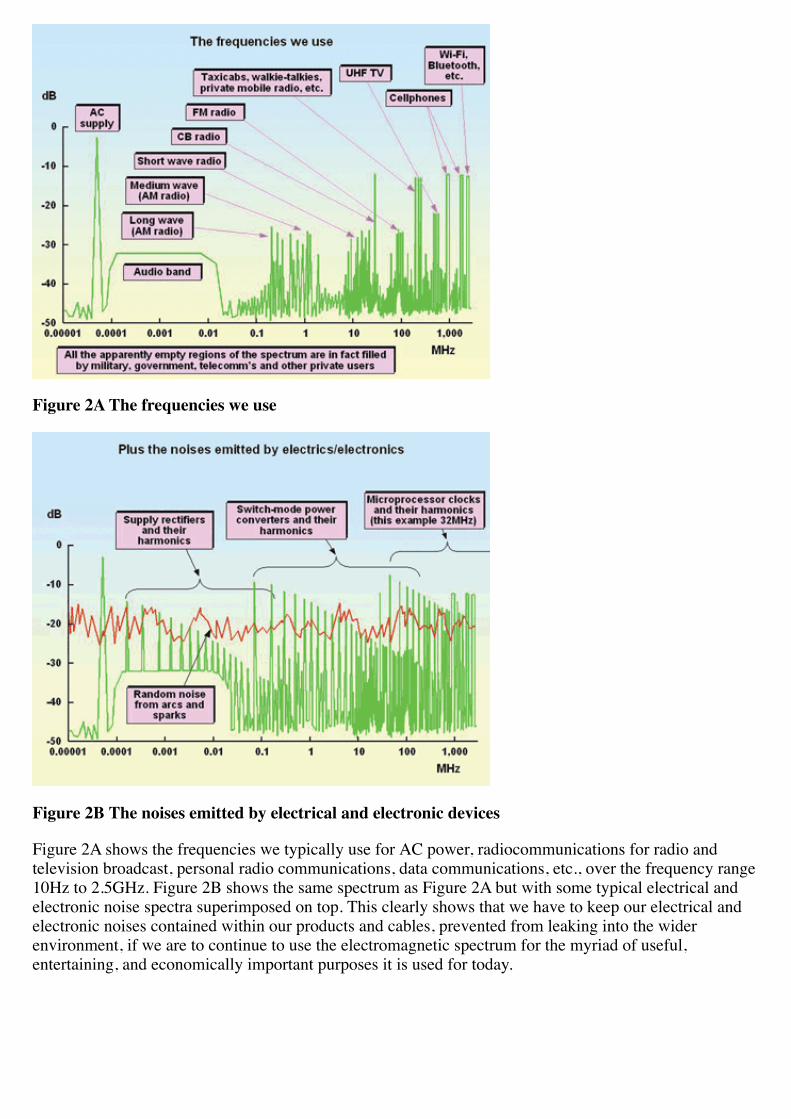
Figure 2A The frequencies we use
Figure 2B The noises emitted by electrical and electronic devices
Figure 2A shows the frequencies we typically use for AC power, radiocommunications for radio andtelevision broadcast, personal radio communications, data communications, etc., over the frequency range10Hz to 2.5GHz. Figure 2B shows the same spectrum as Figure 2A but with some typical electrical andelectronic noise spectra superimposed on top. This clearly shows that we have to keep our electrical andelectronic noises contained within our products and cables, prevented from leaking into the widerenvironment, if we are to continue to use the electromagnetic spectrum for the myriad of useful,entertaining, and economically important purposes it is used for today.

Figure 2C The ’accidental antenna’ behaviour of typical conductors
Figure 2C shows the same spectrum as Figure 2B, but the vertical axis has been changed to metres andlines have been added to show the accidental antenna behaviour of a typical straight conductor in freespace, driven at one end by a low-impedance source and with a high-impedance load at its other end. Suchconductors resonate at frequencies at which their length is an integer multiple of a quarter-wavelength,and at those frequencies they are supremely efficient antennas. Indeed, almost all small portable radiotransmitters and receivers rely on exactly such antennas, known as whip antennas.
The bold line in Figure 2C shows the curve of length versus frequency for a conductor that is one quarterof a wavelength long. Below their first resonance, such conductors convert almost all of the signals theyare carrying at their resonant frequency into electric fields launched into the air, which means there is littlesignal at that frequency left for the load - distorting waveforms and causing signal integrity (SI) problems.The E-fields launched turn into EM-fields in the far field (i.e. at distances greater than λ/6, λ being thewavelength). Such conductors also convert electric fields in their environments (and the electric fieldcomponents of EM-fields) into noise signals in themselves, causing signal integrity (SI) and EMCimmunity problems for their circuits.
There are two other diagonal lines in Figure 2C, one indicating the length of conductor that makes arelatively poor antenna (approximately -20dB efficiency) at a given frequency, and another indicating thelength that makes a very poor antenna (approx. -40dB efficiency). Note that this latter line crosses the axisat 10mm length at a frequency of around 70MHz, showing that for a 10mm long conductor (whether apiece of wire or a cable shield that is only terminated at one end) we might be able to ignore its accidentalantenna behaviour at frequencies below 70MHz - in typical commercial/industrial situations, unless it wascarrying atypically large RF currents. In especially sensitive applications, or in the very harsh EMenvironments of some military and aerospace applications, just 10mm of accidental antenna could causeinterference problems at frequencies as low as 7MHz, and maybe even less.
The above analysis was for a straight conductor on its own, rather like the structure of a whip antenna,and a similar analysis can be applied to another common shape, the loop. Below its first resonance, a loopconductor with a low-impedance source and load emits and picks-up magnetic fields and also picks up themagnetic components of EM-fields. The H-fields it emits turn into EM-fields in the far field. Foraccidental loop antennas, the diagonal lines of accidental antenna efficiency in Figure 2C represent theradius of a circular loop, or half the loop’s longest diagonal dimension.
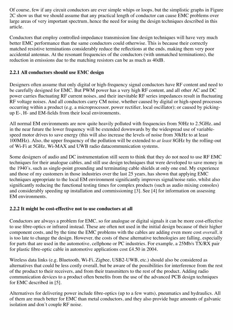
Of course, few if any circuit conductors are ever simple whips or loops, but the simplistic graphs in Figure2C show us that we should assume that any practical length of conductor can cause EMC problems overlarge areas of very important spectrum, hence the need for using the design techniques described in thisarticle.
Conductors that employ controlled-impedance transmission line design techniques will have very muchbetter EMC performance than the same conductors could otherwise. This is because their correctlymatched resistive terminations considerably reduce the reflections at the ends, making them very pooraccidental antennas. At the resonant frequencies of the conductors (with unmatched terminations), thereduction in emissions due to the matching resistors can be as much as 40dB.
2.2.1 All conductors should use EMC design
Designers often assume that only digital or high-frequency signal conductors have RF content and need tobe carefully designed for EMC. But PWM power has a very high RF content, and all other AC and DCpower carries fluctuating RF current noises, and their inevitable RF series impedances result in fluctuatingRF voltage noises. And all conductors carry CM noise, whether caused by digital or high-speed processesoccurring within a product (e.g. a microprocessor, power rectifier, local oscillator); or caused by picking-up E-, H- and EM-fields from their local environments.
All normal EM environments are now quite heavily polluted with frequencies from 50Hz to 2.5GHz, andin the near future the lower frequency will be extended downwards by the widespread use of variable-speed motor drives to save energy (this will also increase the levels of noise from 30kHz to at least100MHz). Also, the upper frequency of the pollution will be extended to at least 8GHz by the rolling-outof Wi-Fi at 5GHz, Wi-MAX and UWB radio datacommunication systems.
Some designers of audio and DC instrumentation still seem to think that they do not need to use RF EMCtechniques for their analogue cables, and still use design techniques that were developed to save money inthe 1940’s, such as single-point grounding and terminating cable shields at only one end. My experienceand those of my customers in those industries over the last 25 years, has shown that applying EMCtechniques appropriate to the local EM environment significantly improves signal/noise ratio, whilst alsosignificantly reducing the functional testing times for complex products (such as audio mixing consoles)and considerably speeding up installation and commissioning [3]. See [4] for information on assessingEM environments.
2.2.2 It might be cost-effective not to use conductors at all
Conductors are always a problem for EMC, so for analogue or digital signals it can be more cost-effectiveto use fibre-optics or infrared instead. These are often not used in the initial design because of their highercomponent costs, and by the time the EMC problems with the cables are adding even more cost overall, itis too late to change the design. However, the costs of these alternative technologies are falling, especiallyfor parts that are used in the automotive, cellphone or PC industries. For example, a 25Mb/s TX/RX pairfor plastic fibre-optic cable in automotive applications cost £4.50 in 2004.
Wireless data links (e.g. Bluetooth, Wi-Fi, Zigbee, USB2-UWB, etc.) should also be considered asalternatives that could be less costly overall, but be aware of the possibilities for interference from the restof the product to their receivers, and from their transmitters to the rest of the product. Adding radiocommunication devices to a product often benefits from the use of the advanced PCB design techniquesfor EMC described in [5].
Alternatives for delivering power include fibre-optics (up to a few watts), pneumatics and hydraulics. Allof them are much better for EMC than metal conductors, and they also provide huge amounts of galvanicisolation and don’t couple RF noise.
Conductors used for safety ’earthing’ or ’grounding’ are covered at the end of this article.
If using metal conductors: products that employ a single PCB with a 0V plane over the whole of its area,and no internal wires at all, are generally the most cost-effective. The 0V plane must underlie all of thecomponents and traces and extend beyond them by at least 3mm on all sides (see Part 4 of [5] for moredetails).
Where multiple PCBs are required in a product, it can even be cost-effective to use flexi-rigid PCBs withan overall 0V plane, because of their EMC benefits. Flexi-rigid PCBs use one or more flexible PCB layersover all their area, plus rigid areas where components are mounted. The flexible areas are really just signaland power interconnections between the rigid areas, but the advantage over a number of PCBs connectedby flexible jumpers, connectors, or cables is that the 0V plane can be continuous over the whole assembly.Flexi-rigid PCB assemblies generally cost more in themselves, but the EMC benefits of their continuous0V planes can save development time and manufacturing costs overall, plus they do not have the cost,size, and unreliability problems associated with electromechanical connectors, and they can be muchquicker to assemble in a product.
2.2.3 Controlling the DM and CM current paths
EMC design techniques for metal conductor interconnects are all about controlling the physical (i.e.geometrical) relationships between the send and return current paths, for both the differential-mode (DM)and common-mode (CM) currents. The DM currents and voltages are our wanted signals or power, whilstCM currents and voltages are associated with the accidental ’leakage’ from our DM signals due to straycapacitance and inductance.
Conversion of DM into CM currents and voltages always happens in any real-life circuit, and in mostapplications is responsible for most of our EMC emissions problems above about 1MHz. The reverseprocess of CM-DM conversion is responsible for most immunity problems above about 1MHz. Theexception is in applications where the metal chassis is used as the DM current return path, where DMcurrents and voltages can be significant above 1MHz. It is very bad EMC practice to use a chassis as aDM current return, but unfortunately this is exactly the method used for heavy loads in motor cars.
It would be ideal for EMC if we could use conductors in which the send and return path were physicallyidentical, because their stray couplings to the rest of the world would then be identical and CM problemsminimised. But of course this is physically impossible (the conductors would short-out), and the nextsection discusses practical cable types.
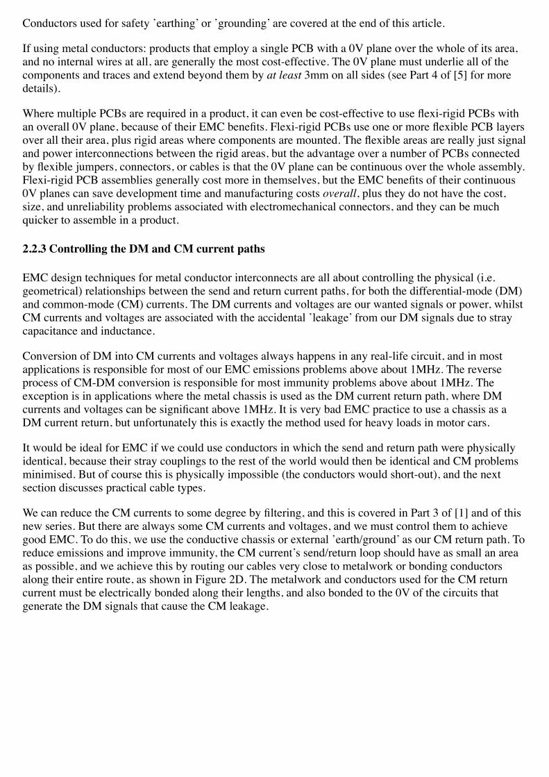
We can reduce the CM currents to some degree by filtering, and this is covered in Part 3 of [1] and of thisnew series. But there are always some CM currents and voltages, and we must control them to achievegood EMC. To do this, we use the conductive chassis or external ’earth/ground’ as our CM return path. Toreduce emissions and improve immunity, the CM current’s send/return loop should have as small an areaas possible, and we achieve this by routing our cables very close to metalwork or bonding conductorsalong their entire route, as shown in Figure 2D. The metalwork and conductors used for the CM returncurrent must be electrically bonded along their lengths, and also bonded to the 0V of the circuits thatgenerate the DM signals that cause the CM leakage.
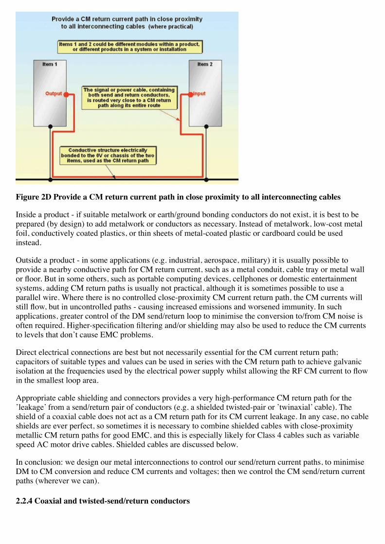
Figure 2D Provide a CM return current path in close proximity to all interconnecting cables
Inside a product - if suitable metalwork or earth/ground bonding conductors do not exist, it is best to beprepared (by design) to add metalwork or conductors as necessary. Instead of metalwork, low-cost metalfoil, conductively coated plastics, or thin sheets of metal-coated plastic or cardboard could be usedinstead.
Outside a product - in some applications (e.g. industrial, aerospace, military) it is usually possible toprovide a nearby conductive path for CM return current, such as a metal conduit, cable tray or metal wallor floor. But in some others, such as portable computing devices, cellphones or domestic entertainmentsystems, adding CM return paths is usually not practical, although it is sometimes possible to use aparallel wire. Where there is no controlled close-proximity CM current return path, the CM currents willstill flow, but in uncontrolled paths - causing increased emissions and worsened immunity. In suchapplications, greater control of the DM send/return loop to minimise the conversion to/from CM noise isoften required. Higher-specification filtering and/or shielding may also be used to reduce the CM currentsto levels that don’t cause EMC problems.
Direct electrical connections are best but not necessarily essential for the CM current return path;capacitors of suitable types and values can be used in series with the CM return path to achieve galvanicisolation at the frequencies used by the electrical power supply whilst allowing the RF CM current to flowin the smallest loop area.
Appropriate cable shielding and connectors provides a very high-performance CM return path for the’leakage’ from a send/return pair of conductors (e.g. a shielded twisted-pair or ’twinaxial’ cable). Theshield of a coaxial cable does not act as a CM return path for its CM current leakage. In any case, no cableshields are ever perfect, so sometimes it is necessary to combine shielded cables with close-proximitymetallic CM return paths for good EMC, and this is especially likely for Class 4 cables such as variablespeed AC motor drive cables. Shielded cables are discussed below.
In conclusion: we design our metal interconnections to control our send/return current paths, to minimiseDM to CM conversion and reduce CM currents and voltages; then we control the CM send/return currentpaths (wherever we can).
2.2.4 Coaxial and twisted-send/return conductors
Coaxial cable is the closest approach to coincident send/return conductors, because the averaged currentflow in the coaxial shield across the cross-section lies along the centre line, where the centre conductor isrouted. But flexible coaxial cables turn out to be less than ideal in practice, for reasons discussed later, andmany manufacturers prefer to use unshielded cables to save cost.
We must always route each send conductor with at least one dedicated return conductor, and make themas close together as possible without compromising insulation requirements, as shown in Figure 2D.
Figure 2E Always provide a return current path physically close to the send path
If we twist the send and return conductors together with a twist-pitch that is much less than one-tenth of awavelength at the highest frequency of concern, the effects of stray capacitances and inductances tend tocancel out, reducing the rate of DM-CM conversion (and CM-DM). Better repeatability twist-to-twistmeans better cancellation and still lower conversion rates.
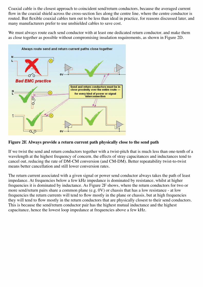
The return current associated with a given signal or power send conductor always takes the path of leastimpedance. At frequencies below a few kHz impedance is dominated by resistance, whilst at higherfrequencies it is dominated by inductance. As Figure 2F shows, where the return conductors for two ormore send/return pairs share a common plane (e.g. 0V) or chassis that has a low resistance - at lowfrequencies the return currents will tend to flow mostly in the plane or chassis, but at high frequenciesthey will tend to flow mostly in the return conductors that are physically closest to their send conductors.This is because the send/return conductor pair has the highest mutual inductance and the highestcapacitance, hence the lowest loop impedance at frequencies above a few kHz.
Figure 2F The send/return current automatically flows in the loop that has the least impedance
This natural, automatic behaviour of the return current results in the best crosstalk and best EMC that ispossible given a particular conductor structure. So all we have to do to make crosstalk, SI and EMC evenbetter is provide lower-impedance return paths - and the return currents will automatically take them andachieve the benefits we want.
When using single-ended signals and power, all the low-impedance return paths appear in parallel withthe reference voltage (typically 0V) on the circuit schematic, which looks like an unnecessary duplicationand is prone to being simplified during ’value analysis’ to save cost - so it is important to mark these onthe drawing as an important EMC design issue, the removal of which will almost certainly add costoverall or cause non-compliance.
Sometimes the return current might flow in one or more DC power supplies as well as in the 0V system(e.g. in a +/-12V analogue system), or might flow in all of the other phases and neutral of a three-phasemains electricity supply. So sometimes we may need to twist more than just a pair of conductors toprovide the return current path, we might have to twist three, four or more wires. For example, a three-phase star-connected mains AC supply should twist five wires - the three phases, neutral and the earth orground.
When very heavy currents are used (e.g. kA) it might not be possible to route the send and returnconductors as close together as we would like for good EMC, because the physical and mechanical forcesacting on the conductors themselves due to the very powerful magnetic fields between them can cause theconductors to damage their insulation. I had the experience of working on a steel rolling mill motor drive,where the motor currents were +/-8kA. To prevent damage to the cables the send and return motorconductors were routed in steel cable trays about two metres apart. The magnetic fields in the nearbycontrol room, resulting from the motor currents in the widely-spaced cables was over 100μT, whichcaused terrible distortion of the images on the cathode-ray type monitors, making the control roomunusable.
The problem could have easily been foreseen by a few back-of-envelope calculations using the verysimple Biot-Savart law, bearing in mind that most such monitors show image movement with more than1æT. But the customer instead relied on the motor drive supplier’s assurances that the drive passed all ofthe EMC Directive standards and was CE marked, and assumed this would guarantee no interference ofany sort. But this article is not the place to discuss the difference between complying with EMC Directive
listed standards, and actually complying with its EMC ’Protection Requirements’. In the end, the problemwas solved by replacing the CRT monitors with liquid crystal flat-panel models. Now that the EMFDirective (1999/519/EC) is in force, and we have associated measurement standards, the human exposurein the control room should be measured and steps taken if it exceeds the limits, but this is also outside thescope of this article.
So the conclusion is that where the send and return path cannot be close together for some good reason,bad EMC effects must be expected and calculations or experiments undertaken to determine their scaleand whether mitigation techniques (shielding, filtering, suppression, etc.) will be required.
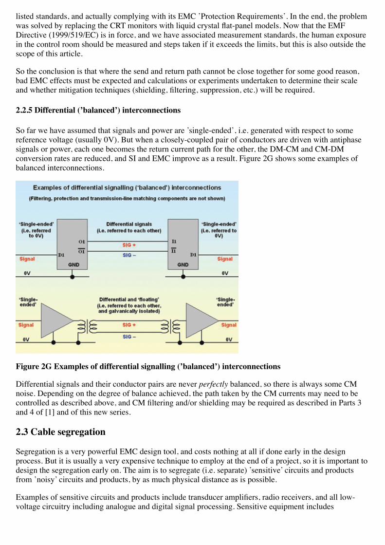
2.2.5 Differential (’balanced’) interconnections
So far we have assumed that signals and power are ’single-ended’, i.e. generated with respect to somereference voltage (usually 0V). But when a closely-coupled pair of conductors are driven with antiphasesignals or power, each one becomes the return current path for the other, the DM-CM and CM-DMconversion rates are reduced, and SI and EMC improve as a result. Figure 2G shows some examples ofbalanced interconnections.
Figure 2G Examples of differential signalling (’balanced’) interconnections
Differential signals and their conductor pairs are never perfectly balanced, so there is always some CMnoise. Depending on the degree of balance achieved, the path taken by the CM currents may need to becontrolled as described above, and CM filtering and/or shielding may be required as described in Parts 3and 4 of [1] and of this new series.
2.3 Cable segregation
Segregation is a very powerful EMC design tool, and costs nothing at all if done early in the designprocess. But it is usually a very expensive technique to employ at the end of a project, so it is important todesign the segregation early on. The aim is to segregate (i.e. separate) ’sensitive’ circuits and productsfrom ’noisy’ circuits and products, by as much physical distance as is possible.
Examples of sensitive circuits and products include transducer amplifiers, radio receivers, and all low-voltage circuitry including analogue and digital signal processing. Sensitive equipment includes

instrumentation and metering, computers and programmable logic controllers, audio, and radio receivers.
’Noisy’ circuits and products include digital signal processing, switch-mode power conversion (DC powersupplies, inverters, PWM, etc.), radio transmitters, RF processing of materials (e.g. plastic welders andsealers, induction heaters), and anything associated with electrical sparking or arcing, such as relays,contactors, switches, and commutator motors.
Notice that computer technology can be both sensitive and noisy. A variable speed motor drive can have anoisy output and also a sensitive input (e.g. from a tachogenerator or position sensor). Radio equipmentcan include a transmitter and a receiver.
To apply the principles of segregation to interconnecting cables, we first sort our cables into ’classes’according to the types of signals they carry...
Class 1: cables carrying very sensitive signals. This can usefully be split into Class 1a for very sensitiveanalogue signals, and Class 1b for very sensitive digital signals.
Class 2: cables carrying slightly sensitive signals.
Class 3: cables carrying slightly interfering signals (the 230VAC mains supply in a typical office ordomestic building would generally be considered to be Class 3).
Class 4: cables carrying strongly interfering signals.
The above four classes are for power and signals at less than 1kVACrms or 1500VDC or peak. We couldallocate Class 5 and 6 to high-voltage electrical supply cables with 1-32kV and above 32kV, respectively,but this article does not cover such high voltages.
Classes 1 and 4 should always use shielded cables and connectors along their entire route. Where this isnot possible, EMC problems should be expected and mitigation measures may need to be applied.
>p>Once we have the cables classified, we segregate their routes according to their class, always keepingthem very close to a CM return path at all times as discussed earlier. There should be as much space aspossible between each class (or sub-class) but it is very difficult indeed to specify what the spacing shouldbe, because it depends upon the types, qualities and lengths of the cables, and the EMC performance ofthe electrical and electronic circuits connected to them.
However, a very crude guide for cables of 500mm long or more is to separate parallel runs of cables insideproducts by at least 100mm between classes 1-2, 2-3 or 3-4. This means 200mm between classes 1-3 or 2-4, and 300mm between 1 and 4, as shown in Figure 2H. For parallel cable runs outside a product up to30m long and close to CM return path - use at least 150mm between classes 1-2 and 3-4, but 300mmbetween classes 2-3. For more than 30m, increase these spacings proportionally (e.g. doubling them for arun of 60m).
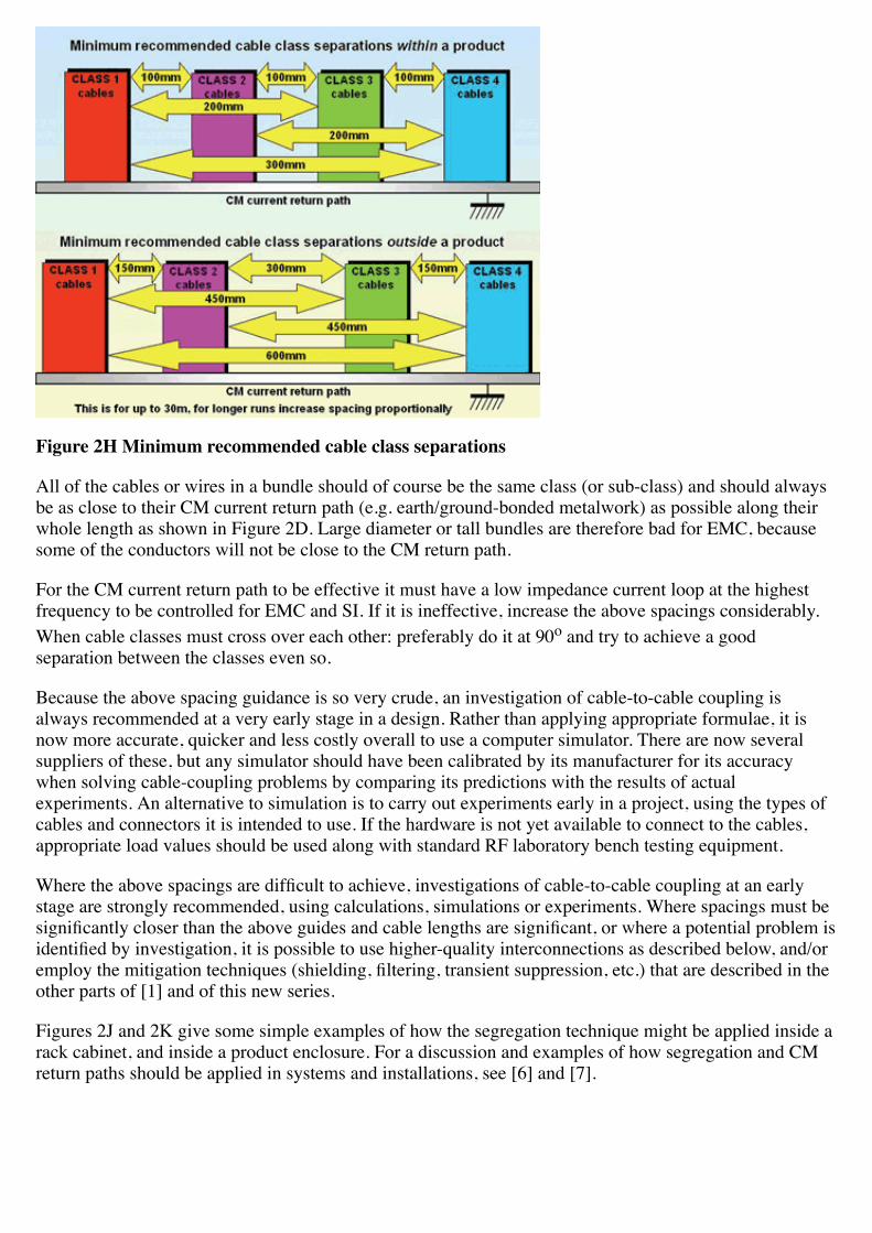
Figure 2H Minimum recommended cable class separations
All of the cables or wires in a bundle should of course be the same class (or sub-class) and should alwaysbe as close to their CM current return path (e.g. earth/ground-bonded metalwork) as possible along theirwhole length as shown in Figure 2D. Large diameter or tall bundles are therefore bad for EMC, becausesome of the conductors will not be close to the CM return path.
For the CM current return path to be effective it must have a low impedance current loop at the highestfrequency to be controlled for EMC and SI. If it is ineffective, increase the above spacings considerably.When cable classes must cross over each other: preferably do it at 90o and try to achieve a goodseparation between the classes even so.
Because the above spacing guidance is so very crude, an investigation of cable-to-cable coupling isalways recommended at a very early stage in a design. Rather than applying appropriate formulae, it isnow more accurate, quicker and less costly overall to use a computer simulator. There are now severalsuppliers of these, but any simulator should have been calibrated by its manufacturer for its accuracywhen solving cable-coupling problems by comparing its predictions with the results of actualexperiments. An alternative to simulation is to carry out experiments early in a project, using the types ofcables and connectors it is intended to use. If the hardware is not yet available to connect to the cables,appropriate load values should be used along with standard RF laboratory bench testing equipment.
Where the above spacings are difficult to achieve, investigations of cable-to-cable coupling at an earlystage are strongly recommended, using calculations, simulations or experiments. Where spacings must besignificantly closer than the above guides and cable lengths are significant, or where a potential problem isidentified by investigation, it is possible to use higher-quality interconnections as described below, and/oremploy the mitigation techniques (shielding, filtering, transient suppression, etc.) that are described in theother parts of [1] and of this new series.
Figures 2J and 2K give some simple examples of how the segregation technique might be applied inside arack cabinet, and inside a product enclosure. For a discussion and examples of how segregation and CMreturn paths should be applied in systems and installations, see [6] and [7].

Figure 2J Example of segregation in a 19" rack cabinet
Figure 2K Example of segregation inside a product’s enclosure
Where ’noisy’ and ’sensitive’ circuits or products must interconnect, the sensitive one is at risk fromconducted DM and CM noise from the noisy one. This is best avoided by using galvanic isolationtechniques suitable for the frequency range of the noise, including:
Isolating transformersOpto-isolators or opto-couplersFibre-optics (using cables that contain no metal, e.g. for pulling strength, vapour barriers or armour)Infra-red communicationsWireless communicationsFree-space microwave or laser communications

Any conductive interconnections between noisy and sensitive units will need to be mitigated (e.g. byshielding, filtered, transient/surge suppression, etc.) to reduce the potentially interfering DM and CMnoises on the conductors to acceptable levels.
2.4 Unshielded interconnections
2.4.1 Unshielded wires and cables
Unshielded conductors can be quite good for EMC - providing they use the twisted-send/return techniquedescribed above, and have connectors that maintain close proximity between their send and return pins.But shielded twisted-pairs are better, and are discussed below.
Some manufacturers prefer to use bundles of single conductors, or ribbon cables that can be mass-terminated, because they require less time (hence costs) during assembly, and are more easily automated,than twisted-pairs. Although such conductors have poor EMC performance (for both ’internal’ and’external’ EMC), they can be designed to obtain the best EMC performance they are capable of. Thishelps reduce the cost of the product by easing filtering and shielding requirements, and helps avoid delaysby reducing the number of design iterations.
The EMC performance of bundles of single conductors can be improved considerably by including anumber of additional return wires in the bundle, as shown in Figure 2L. These extra conductors must havelow-impedance RF bonds (e.g. direct connections or series capacitors) to the reference planes (e.g. 0V) orchassis at both ends of the bundle. The additional wires should ideally be distributed regularly throughoutthe bundle, and with nearly as many additional wires as there are original signal or power wires theimprovement in EMC can be more than 10dB up to at least 200MHz.
Figure 2L Improving wire bundles and flat cables
The EMC performance of ribbon cables can be improved markedly, by adding return conductors. Eachsignal or power conductor should have at least one return conductor adjacent to it, so the minimumimplementation is: return, signal, signal, return, signal, signal, return, ..etc. as shown in Figure 2L. But thebest implementation is: return, signal, return, signal, return, signal, ..etc., also as shown in Figure 2LMaking the outermost two conductors in a ribbon cable return, not signal or power, can also help. Powerconductors are treated as if they were signals.
Unshielded wires and cables that are implemented using correctly-matched controlled-impedancetransmission lines will have very much better EMC performance than the same wires could otherwise.This is because their correctly matched resistive terminations considerably reduce the reflections at theends, making them very poor accidental antennas. At the resonant frequencies of the (unmatched)conductors, the reduction in emissions due to matching can be as much as 40dB. Transmission-line designwill be discussed in the second instalment of this article.
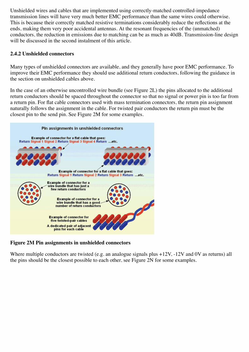
2.4.2 Unshielded connectors
Many types of unshielded connectors are available, and they generally have poor EMC performance. Toimprove their EMC performance they should use additional return conductors, following the guidance inthe section on unshielded cables above.
In the case of an otherwise uncontrolled wire bundle (see Figure 2L) the pins allocated to the additionalreturn conductors should be spaced throughout the connector so that no signal or power pin is too far froma return pin. For flat cable connectors used with mass termination connectors, the return pin assignmentnaturally follows the assignment in the cable. For twisted pair conductors the return pin must be theclosest pin to the send pin. See Figure 2M for some examples.
Figure 2M Pin assignments in unshielded connectors
Where multiple conductors are twisted (e.g. an analogue signals plus +12V, -12V and 0V as returns) allthe pins should be the closest possible to each other, see Figure 2N for some examples.

Figure 2N Example of an unshielded 10-way connector carrying signals and power
2.5 Earthing and grounding conductors
This article is about signal and power interconnections, but it is worth saying a few words about earthingand grounding, because this is usually done with conductors.
The purpose of earthing and grounding of products is to ensure personnel safety and protection of theinstallation against damage. The main consideration for safety earths and grounds are power system faultsand lightning, with typical currents being 10kA or more.
To function as an effective earth/ground, the installation’s earth/ground structure must have a lowimpedance at the highest frequency of concern. Traditional building installation earth/ground structuresuse long conductors to connect to a single point of connection (the main earth/ground terminal or bar).10m (40 feet) of wire has an impedance of about 1W at about 16kHz, so we can see that such structuresare generally ineffective for EMC above a few tens of kHz. Figure 2C also shows us that a 10m wire startsto behave as a significant accidental antenna above about 75kHz, which makes it no kind of earth/groundat all at such frequencies.
To have some useful effect on higher frequencies requires a meshed conductive earth/ground structure; forexample, a 1m mesh size provides a low-impedance earth/ground structure up to about 1MHz. But sheetmetal earth/ground structures, typical of traditional aircraft, ships, oil and gas platforms, etc., are evenbetter than meshes, and can provide low impedance earths/grounds up to hundreds of MHz.
But the only effective RF earth/ground is a local one, so to be of any use at all for EMC a low impedanceearth/ground structure in an installation should be closer to the product to be grounded than one-tenth of awavelength at the highest frequency of concern. For a good quality earth/ground connection, the productshould be even closer to the low-impedance ground structure, maybe one-hundredth of a wavelength orless.
Assuming that we had a perfect low-impedance earth/ground structure in the installation our product isintended for, and our product was close enough to it, we still need to make our connection between theproduct and the earth/ground with a low enough impedance, and without resonances in the frequencyrange of concern. For example, a 600mm square cabinet on insulated feet 10mm above a sheet metalearth/ground floor will have a stray capacitance of approximately 0.4nF between the cabinet and the floor.
Bonding them together with 100mm of round wire, or 150mm of braid strap has an inductanceapproximately 100nH, resulting in a parallel resonance with the stray capacitance at around 25MHz -making its EMC worse around this frequency than if there was no connection at all between the cabinetand the installation’s earth/ground. The only RF bonding that is truly effective up to 1GHz or more isdirect metal-to-metal contact, preferably at multiple points, ideally seam-soldered or seam-welded.
So the EMC effects of connecting a product to the earth/ground in its installation depends on how theearth/ground structure is implemented and its impedance versus frequency characteristics; plus the straycapacitance between the product and the earth/ground and the inductance associated with the connectionbetween the product and the earth/ground.
Typical building installations constructed using single-point earthing/grounding with long conductors areuseless as EMC earth/grounds above a few tens of kHz. Meshed ground structures with multiple veryshort conductors or braids connecting to a product’s chassis can be made to be effective up to tens ofMHz, and large areas of sheet metal with the product’s chassis bolted directly to it at multiple points canbe a very effective ground up to hundreds of MHz. To be more precise than this requires a detailedanalysis of the structures and conductors concerned, and the shape and location of the product.
2.6 Shielded (screened) cables
2.6.1 How do we shield a wire or cable?
Like any electromagnetic (EM) shields, shielded cables and connectors have a metal layer (the shield)around all of the conductors to be shielded. For good shielding performance, they need 360o shieldcoverage along their entire length, including at all connectors, glands or joints. The phrase: "360o shieldcoverage" is sometimes called peripheral or circumferential shield coverage, and these terms are appliedto shielded cables of any cross-sectional shape, whether they are round, flat, or whatever. 360o shieldcoverage means that there are no gaps or regions of high conductivity in the shield’s material all aroundthe cross-section of the cable and its connectors or glands.
For good shielding performance the electrical bonding between a cable’s shield and the shields of itsconnectors or glands and any shielded enclosures should have no gaps in it either. This means that thereshould be a seamless low-impedance electrical connection all around the perimeter or circumference ofthe electrical joint. This is often referred to as 360o shield bonding, and it applies between a cable shieldand connector shield, the shields of two mating connectors, and also between the shield of a connectorand the metal chassis or structure it is mounted on.
It can help to think of shielding cables as plumbing with copper pipes - if there are any gaps in the 360o
surface of the metal pipes or its connectors and glands, or in their soldered or metal-to-metal compressionjoints, the water will leak out. If we substitute EM-field leakage for water leakage we have a usefulanalogy. The higher the frequency, the higher the field leakage rate through a given shield imperfection, sowe could make an analogy between higher frequencies and higher water pressures. But it doesn’t do tostretch the analogy very far, because EM-fields also leak into a cable at its shield imperfections; and thereis no EM analogy for preventing water leakage with a rubber washer.
The metal shielding layer is ideally made of a solid metal. This makes the cable inflexible, but this can beacceptable where cables lie in fixed routes, for example products often use ’microwave semi-rigid’ cablesfor the fixed wiring for their microwave signals.
Flexible shielded cables either use a metallised plastic tape wound around the conductors to be shielded(usually called ’foil shielded’), or a braided wire tube (’braid shielded’). Multiple shields are also used,typically two braids in contact with each other, or braid and foil. Because the foil shield is wound as ahelix, the metallised layers do not make contact between the turns, so a ’drain wire’ is used to short each

turn of the foil to its neighbour. In a braid and foil shielded cable, it is best if the braid is on the metallisedside of the plastic foil, because this connects the foil’s turns to each other better.
All flexible shielded cables have ’leakage’ problems because they don’t use a solid metal shield. Theimperfections in flexible shields have associated stray capacitance and stray inductance, and it is possibleto ’optimise’ a braid so that these effects cancel out to some extent.
Special cables are also available with multiple insulated shields, in which the different shields do notmake contact with each other (e.g. Triaxial). Even more exotic (and expensive) are ’superscreened’flexible cables, which combine one or more metal shields with one or more high-permeability metal tapeswound around the conductors.
Some connectors use multi-point bonding for their shields, instead of 360o bonding. The more bondingpoints there are, the better the shielding will be, with continuous bonding around the whole circumferencebeing the best.
2.6.2 How shielded interconnections work
When a shield interacts with an EM-field, currents flow in the shield. ’Skin Effect’ makes RF currentstravel on the surface of a shield, with current density diminishing with depth into the shield’s metal by36% for every ’skin depth’. The higher the frequency, or the more conductive the metal of the shield, thesmaller is the skin depth. For good shielding effectiveness the shield should have many skin depths ofthickness at the lowest frequency to be shielded. Skin effect is not described further here, but a usefulreference is [8]. Figure 2P shows that providing we achieve our 360o shield coverage and 360o electricalbonding at shield joints, and have enough thickness in our shield’s metal given the frequency, the skineffect tends to force the ’external’ surface currents to flow on the outside of the shield, and the ’internal’
surface currents on the inside.
Figure 2P Skin effect and its effect on cable and connector shielding
The external surface currents shown by Figure 2P are created by the interaction of the shield with itsexternal EM environment, and they are CM currents. For good immunity we must ensure that their currentdensity in the shield material is very low indeed by the time they reach its inner surface.
Still referring to Figure 2P, the internal surface currents are created by the CM currents leaking from theDM signals or RF noise in the send/return conductor twisted pair. For low emissions we must ensure that
their current density in the shield material is very low indeed by the time they reach its outer surface.
The inner surface of the shield makes an ideal low-impedance CM return path for the interconnection, andit is important to complete the loop by connecting the shield to the electronic circuit where the DM signalsor RF noise originated. This is shown in Figure 2P as a direct connection between the PCB’s referenceplane (usually a 0V plane for analogue or digital signals) and the chassis that the shielded connector ismounted upon. As mentioned earlier, the CM current path can be completed by series capacitors insteadof direct connection, where galvanic isolation is required (e.g. for automotive applications, or off-linemains power supplies).
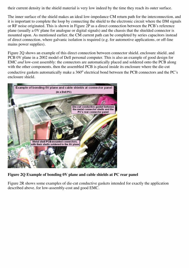
Figure 2Q shows an example of this direct connection between connector shield, enclosure shield, andPCB 0V plane in a 2002 model of Dell personal computer. This is also an example of good design forEMC and low-cost assembly: the connectors are automatically placed and soldered onto the PCB alongwith the other components, then the assembled PCB is placed inside its enclosure where the die-cutconductive gaskets automatically make a 360o electrical bond between the PCB connectors and the PC’senclosure shield.
Figure 2Q Example of bonding 0V plane and cable shields at PC rear panel
Figure 2R shows some examples of die-cut conductive gaskets intended for exactly the applicationdescribed above, for low-assembly-cost and good EMC.

Figure 2R Some examples of die-cut conductive gaskets
2.6.3 Why coaxial cables aren’t very cost-effective for EMC
In the shielded twisted-pair of Figure 2P, the shield only carries CM currents, which are typically 100 to1000 times smaller than the DM currents, depending on the ’balance’ of the twisted-pair. But in coaxialcables the DM return current itself flows on the inside surface of the shield, so the resulting ’leakage’current density on the outer surface of the shield, responsible for creating the emissions, is much largerthan it would be for a twisted-pair with the same type of shield.
Also, in a coaxial cable the current density on the inside surface of the shield resulting from the diffusionof the external CM currents adds a noise voltage in series with the return path of the DM signal, which isthe same as adding the same noise voltage into the send path of the wanted signal. So coaxial cable is notas good for immunity as the same shield over a twisted-pair either.
Coaxial cables with solid and thick metal shields have very good EMC performance indeed, for bothemissions and immunity, but they are not flexible so are not generally used. There are some types offlexible coaxial cables that achieve good EM performance by using double-layer shields and othertechniques, such as ’superscreening’, but at a price. So coaxial cables are not preferred when we needgood EMC at a low cost - shielded twisted-pairs are better.
2.6.4 The ZT and Shielding Effectiveness (SE) of various types of cable
SE is defined as the ratio (in dB) of the field emitted without the shield, compared with the field emittedwith the shield. Measuring this accurately can be quite tricky, so it is more usual to measure the surfacetransfer impedance: ZT. ZT is measured in test jigs that inject a surface current into the cable’s shield, andmeasure the noise voltage resulting on the inner conductors. The ratio of the measured noise voltage to theinjected shield current is ZT, in Ω. These tests are more easy to set up to give accurate results, so when wewant a cable with a good SE, we choose one with a low value of ZT over the frequency range we areconcerned about.
One formula relating ZT to SE is: SE = 36 - 20log10L - 20log10ZT, where L is the cable’s length in metresand ZT is in Ω/m. But because of the variety of definitions and measuring methods for SE, this simple

equation might not predict the SE actually measured.
Figure 2S shows some test results for different types of coaxial cable, taken from figure A2 of Def Stan59-41 Part 7/1 Annex A. I would expect a shielded twisted-pair to have a usefully lower ZT (higher SE)than a coaxial cable with the same design of shield.
Figure 2S The ZT of different types of coaxial cable
As Figure 2S shows, a lower shield resistance (more metal in the shield) reduces ZT and hence improvesSE at frequencies below 1MHz. Above 1MHz, it is clear that all flexible shielded cables suffer from’leakages’ that increase their ZT (reduce their SE) above a frequency that generally lies somewherebetween 1 and 100MHz. Even ’superscreened’ cables show this behaviour, except for the more costlytypes. [9] has a lot more information on the SE and ZT of various cables.
However, cables with solid metal shields (e.g. microwave ’semi-rigid’, and solid metal circular conduitwith 360o bonds at all joints and both ends) have a ZT that continually reduces as the frequency increases.This is because with solid metal shields, skin effect can work to its fullest extent, keeping internal CMsurface currents inside, and external CM surface currents outside.
2.6.5 More on designing shielded interconnections
The 2nd Instalment of this article will continue discussing the design of shielded interconnections.
2.7 Transmission line interconnections
This topic will be covered in the 2nd Instalment of this article.
2.8 References
[1] Keith Armstrong, "Design Techniques for EMC", UK EMC Journal, a 6-part series publishedbimonthly February - December 1999. An improved version of this original series is available via the"Publications & Downloads" page at http://www.cherryclough.com[2] The Institution of Electrical Engineers (IEE), Professional Network on Functional Safety, "EMC and

Functional Safety Resource List", via the "Publications & Downloads" page athttp://www.cherryclough.com[3] The articles in the "EMC for Pro-Audio" section of the "Publications & Downloads" page athttp://www.cherryclough.com [4] Keith Armstrong, "Assessing an EM Environment", includes informative tables, an example of aninitial questionnaire, guidance and useful references, available via the "Publications & Downloads" pageat http://www.cherryclough.com[5] Keith Armstrong, "Advanced PCB Design and Layout Techniques for EMC", an 8-part seriespublished in the EMC & Compliance Journal, March 2004 - November 2005. An improved version of thisseries is available via the "Publications & Downloads" page at http://www.cherryclough.com.[6] Keith Armstrong, "EMC for Systems and Installations", a 6-part series published in theEMC+Compliance Journal, January-December 2000, also available via the "Publications & Downloads"page at http://www.cherryclough.com.[7] Tim Williams and Keith Armstrong, "EMC for Systems and Installations", Newnes 2000, ISBN 07506 4167 3, www.newnespress.com, RS Components Part No. 377-6463.[8] Skin Depth formula and material properties:http://www.rfcafe.com/references/_spreadsheets/skin_depth_calc_ss.htm[9] Lothar O (Bud) Hoeft, "Analysis of Electromagnetic Shielding of Cables and Connectors (keepingcurrents/voltages where they belong)", IEEE EMC Symposium 2002, Minneapolis,www.emcinfo.se/ieee/protokoll/ 34/EMag_Shielding_of_Cables _and_Connectors
2.9 Acknowledgements
I am very grateful to the following people for suggesting a number of corrections, modifications andadditions to the first series published in 1999: Feng Chen, Kevin Ellis, Neil Helsby, Alan Keenan, MikeLangrish, Tom Liszka, Tom Sato, and John Woodgate.
Eur Ing Keith Armstrong CEng MIEE MIEEEPartner, Cherry Clough Consultants, www.cherryclough.com, Member EMCIA Phone: +44 (0)1457 871 605, Fax: +45 (0)1457 820 145, Email: [email protected]