Embed Size (px)
Citation preview
Design, Simulation, Fabrication and Characterization of Optical Metasurface
by
Mao Ye
A dissertation submitted in partial fulfillment
of the requirements for the degree of
Doctor of Philosophy
(Electrical and Computer Engineering)
in the University of Michigan-Dearborn
2019
Doctoral Committee:
Professor Ya Sha Yi, Chair
Professor Wei Lu
Professor Pravansu Mohanty
Professor Weidong Xiang

ii
Acknowledgements
Firstly, I would like to thank to Prof. Yasha Yi, for his guidance and support through all the five
years of my PhD study. It was a great pleasure to learn academics and much more than
academics from him. Thanks for numerous discussion and idea exchange happening at our lab
and his cozy office. His sharp advices and remarkable help concluding all the publications
contained in this dissertation. I really appreciate it!
For willing to be on my doctoral committee and for helpful comments on my research, I
thank Prof. Pravansu Mohanty, Prof. Weidong Xiang, and Prof. Lu Wei. I also thank my lab
mates Dachuan Wu, Yueheng Peng, Wei Guo, Xiaopeng Guo, and Duomai Zhang for the help
and support through all these years.
Furthermore, I am greatly thankful to the excellent cooperation with all my coauthors,
many colleagues in Umich and Lurie Nano Fabrication. Special thanks to Dr. Vishva Ray for
providing training and turoring at LNF. Of course, there is a huge research community of many
people and friends who supported me deeply. I don’t have the space to thank everyone I met
during my doctoral journey, but they’ve all made me stronger and wiser throughout all these
years of study.
iii
Table of Contents
Acknowledgements ......................................................................................................................... ii
List of Figures ................................................................................................................................. v
Abstract ……………………………………………………………………………………………………………..xi
Chapter 1 Introduction .................................................................................................................... 1
Chapter 2 Simulation Method (FDTD and RCWA) ....................................................................... 7
Chapter 3 Design of Optical Metasurface ..................................................................................... 10
Chapter 4 Nano Fabrication Method Metasurface ........................................................................ 15
Chapter 5 Silicon-rich Silicon Nitride Thin Films for Metalens .................................................. 17
Chapter 6 Linear Polarization Distinguishing Metalens in Visible Wavelength .......................... 30
Chapter 7 Continuous Achromatic Flat Subwavelength Grating Lens over whole Visible
Bandwidths .................................................................................................................... 43
Chapter 8 Transmission Enhancement of Subwavelength Grating Micro Lens by Tapered Nano
Structure ........................................................................................................................ 55
Chapter 9 Taper Resistant Subwavelength Grating Micro Lens .................................................. 65
Chapter 10 Low Contrast Subwavelength Grating Lenses ........................................................... 75
Chapter 11 Influence of Grating Thickness in Low Contrast Subwavelengths Grating
Concentrating Lenses .................................................................................................. 84

iv
Chapter 12 Artificial Focus Pattern Theory .................................................................................. 90
References ................................................................................................................................... 101
Appendix ..................................................................................................................................... 104
v
List of Figures
Figure 1: Illustration of metalens compared with traditional lens compared with traditional lens 4
Figure 2: Space discretization method. (a) Square space discretization. (b) Hexagon space
discretization. ............................................................................................................... 11
Figure 3: schematic diagram for metalens (propagation phase based) cross-section. (a) Large
pitch size. (b) Small pitch size. .................................................................................... 12
Figure 4: Illustration of nano fabrication process ......................................................................... 16
Figure 5: n & k of silicon rich silicon nitride thin films deposited with different N2/Ar
concentration (shown as percentage) through PVD. (a) Refractive index n. (b)
Extinction coefficient k. ............................................................................................... 20
Figure 6: n & k of silicon rich silicon nitride thin films deposited with different SiH4 and NH3
concentration through PECVD. (a) refractive index n. (b) Extinction coefficient k. .. 21
Figure 7: (a) Fabrication-limited phase coverage of 220 nm-pitch phase shifters. (b) Focus
efficiency of simulated metalens (NA=0.9) in 2-D with pitch size (period) ranging
from 220 nm to 360 nm. (c) Field distribution of 2D metalens designed with 220 nm
pitch size....................................................................................................................... 24
Figure 8: SEM picture at center of lens (5×5 µm) ........................................................................ 25
Figure 9: Schematic diagraph for characterization system. (b) Characterized field distribution at
the plane of focus. (c) Focus profile of the SiNx based metalens. ............................... 27
vi
Figure 10: Structure of traditional phase shifter for linear polarized incidence. (b) Structure of
linear polarization distinguishing phase shifter. (c) Design layout of polarization
distinguishing metalens .............................................................................................. 33
Figure 11: Phase and Transmission Diagram for linear polarization distinguishing phase shifters.
(a) Phase diagram for Ez incidence. (b) Transmission for Ez incidence. (c) Phase
diagram for Hz incidence. (d) Transmission for Hz incidence. Period between dashed
lines are periods exhibit strong linear polarization distinguishing effect................... 34
Figure 12: Field distribution at cross-section x=0 of the lens at Ez and Hz incidence. (a) Field
distribution under incidence of Ez Polarization. (b) Field distribution under incidence
of Hz polarization. Lens plane is marked as red line. (c) Field distribution of lens
when Ez is incident. (d) Field distribution of lens when Hz is incident. Lens
structures are confined within red dash line. Lens structures are within the
area marked by red dash lines. ............................................................................... 35
Figure 13: SEM image of polarization distinguishing lens. (a) overall view of the lens, with scale
bar of 5 µm (b) magnified view at the center of lens with scale bar of 1 µm. ........... 39
Figure 14: Characterization system consists of diode laser, linear polarizer (LP), quarter
waveplate (QWP), 50x objective, tube lens (TL) and camera. .................................. 40
Figure 15: Optical characterization of linear polarization distinguishing metalens under Ez (a)
polarized incidence and Hz (b) polarized incidence. (c) Focus profile of both incident
polarizations ............................................................................................................... 41
Figure 16: (a-c) Field distribution of GaN metalens with wavelength of 435 nm (a), 585 nm (b),
and 685 nm (c). Intensity is normalized by the intensity of incident light. (d) Phase
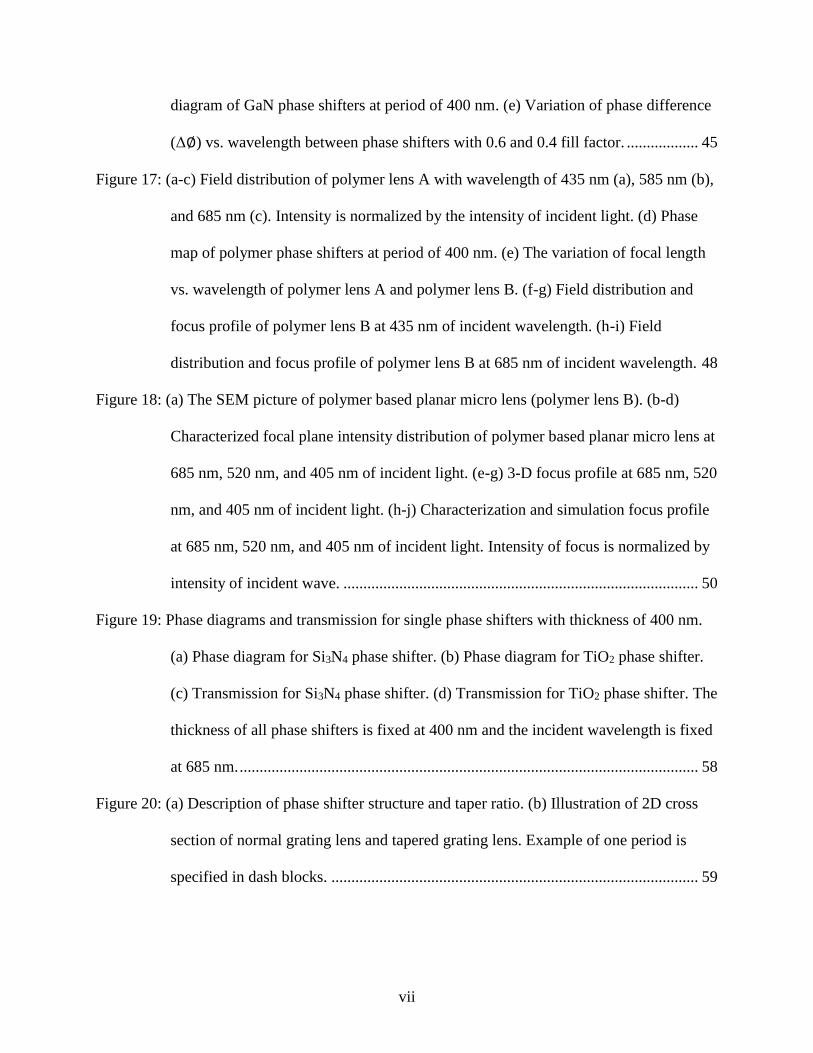
vii
diagram of GaN phase shifters at period of 400 nm. (e) Variation of phase difference
(Δ∅) vs. wavelength between phase shifters with 0.6 and 0.4 fill factor. .................. 45
Figure 17: (a-c) Field distribution of polymer lens A with wavelength of 435 nm (a), 585 nm (b),
and 685 nm (c). Intensity is normalized by the intensity of incident light. (d) Phase
map of polymer phase shifters at period of 400 nm. (e) The variation of focal length
vs. wavelength of polymer lens A and polymer lens B. (f-g) Field distribution and
focus profile of polymer lens B at 435 nm of incident wavelength. (h-i) Field
distribution and focus profile of polymer lens B at 685 nm of incident wavelength. 48
Figure 18: (a) The SEM picture of polymer based planar micro lens (polymer lens B). (b-d)
Characterized focal plane intensity distribution of polymer based planar micro lens at
685 nm, 520 nm, and 405 nm of incident light. (e-g) 3-D focus profile at 685 nm, 520
nm, and 405 nm of incident light. (h-j) Characterization and simulation focus profile
at 685 nm, 520 nm, and 405 nm of incident light. Intensity of focus is normalized by
intensity of incident wave. ......................................................................................... 50
Figure 19: Phase diagrams and transmission for single phase shifters with thickness of 400 nm.
(a) Phase diagram for Si3N4 phase shifter. (b) Phase diagram for TiO2 phase shifter.
(c) Transmission for Si3N4 phase shifter. (d) Transmission for TiO2 phase shifter. The
thickness of all phase shifters is fixed at 400 nm and the incident wavelength is fixed
at 685 nm. ................................................................................................................... 58
Figure 20: (a) Description of phase shifter structure and taper ratio. (b) Illustration of 2D cross
section of normal grating lens and tapered grating lens. Example of one period is
specified in dash blocks. ............................................................................................ 59
viii
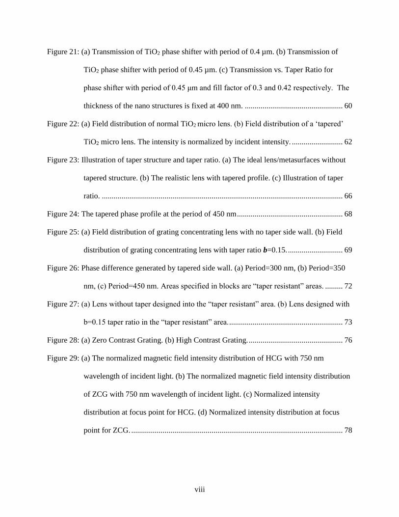
Figure 21: (a) Transmission of TiO2 phase shifter with period of 0.4 µm. (b) Transmission of
TiO2 phase shifter with period of 0.45 µm. (c) Transmission vs. Taper Ratio for
phase shifter with period of 0.45 μm and fill factor of 0.3 and 0.42 respectively. The
thickness of the nano structures is fixed at 400 nm. .................................................. 60
Figure 22: (a) Field distribution of normal TiO2 micro lens. (b) Field distribution of a ‘tapered’
TiO2 micro lens. The intensity is normalized by incident intensity. .......................... 62
Figure 23: Illustration of taper structure and taper ratio. (a) The ideal lens/metasurfaces without
tapered structure. (b) The realistic lens with tapered profile. (c) Illustration of taper
ratio. ........................................................................................................................... 66
Figure 24: The tapered phase profile at the period of 450 nm ...................................................... 68
Figure 25: (a) Field distribution of grating concentrating lens with no taper side wall. (b) Field
distribution of grating concentrating lens with taper ratio b=0.15. ............................ 69
Figure 26: Phase difference generated by tapered side wall. (a) Period=300 nm, (b) Period=350
nm, (c) Period=450 nm. Areas specified in blocks are “taper resistant” areas. ......... 72
Figure 27: (a) Lens without taper designed into the “taper resistant” area. (b) Lens designed with
b=0.15 taper ratio in the “taper resistant” area. .......................................................... 73
Figure 28: (a) Zero Contrast Grating. (b) High Contrast Grating. ................................................ 76
Figure 29: (a) The normalized magnetic field intensity distribution of HCG with 750 nm
wavelength of incident light. (b) The normalized magnetic field intensity distribution
of ZCG with 750 nm wavelength of incident light. (c) Normalized intensity
distribution at focus point for HCG. (d) Normalized intensity distribution at focus
point for ZCG. ............................................................................................................ 78

ix
Figure 30: (a1-4) Concentration forming procedure using HCG lenses. (b1-4) Concentration
forming procedure using ZCG lenses. ....................................................................... 79
Figure 31: (a) Intensity distribution of ZCG with waveguide layer thickness of 0.5 µm. (b)
Intensity distribution of ZCG with waveguide layer thickness of 1 µm. (c) Intensity
distribution of ZCG with waveguide layer thickness of 2 µm. .................................. 82
Figure 32: (a) Field distribution at 750 nm source of 100 nm grating thickness. (b) Magnetic field
distribution at 750 nm source of 200 nm grating thickness. (c) Magnetic field
distribution at 750 nm source of 400 nm grating thickness. (d) Magnetic field
distribution at 750 nm source of 600 nm grating thickness. (e) Magnetic field
distribution at 750 nm source of 800 nm grating thickness. (f) Magnetic field
distribution at 750 nm source of 1000 nm grating thickness. .................................... 85
Figure 33: The normalized magnetic field intensity distribution at 750 nm source of 100 nm
grating thickness. (b) The normalized magnetic field intensity distribution at 750 nm
source of 200 nm grating thickness. (c) The normalized magnetic field intensity
distribution at 750 nm source of 400 nm grating thickness. (d) The normalized
magnetic field intensity distribution at 750 nm source of 600 nm grating thickness.
(e) The normalized magnetic field intensity distribution at 750 nm source of 800 nm
grating thickness. (f) The normalized magnetic field intensity distribution at 750 nm
source of 1000 nm grating thickness. ......................................................................... 86
Figure 34: (a) Illustration of 3-D off axis metalens. (b) The field distribution of x-y focus plane
when off-axis focus moved to (-2, -2) at z = c (focus plane). (c) The field distribution
of of x-z plane. ........................................................................................................... 91
x
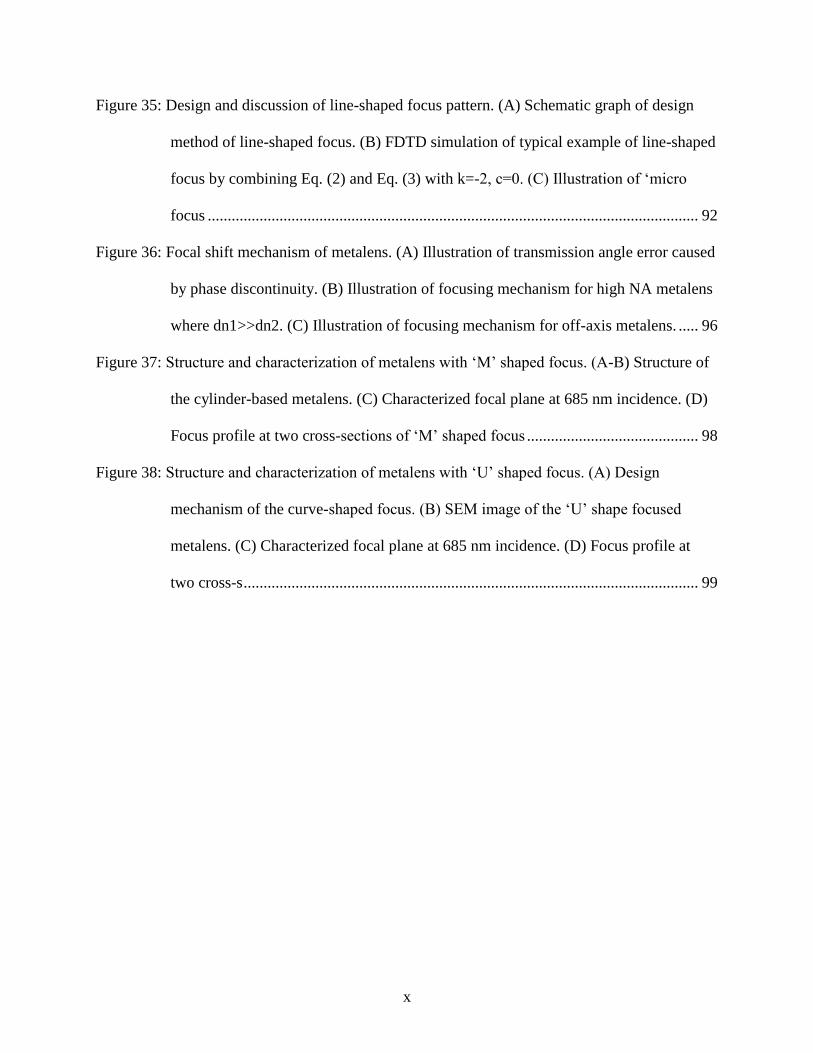
Figure 35: Design and discussion of line-shaped focus pattern. (A) Schematic graph of design
method of line-shaped focus. (B) FDTD simulation of typical example of line-shaped
focus by combining Eq. (2) and Eq. (3) with k=-2, c=0. (C) Illustration of ‘micro
focus ........................................................................................................................... 92
Figure 36: Focal shift mechanism of metalens. (A) Illustration of transmission angle error caused
by phase discontinuity. (B) Illustration of focusing mechanism for high NA metalens
where dn1>>dn2. (C) Illustration of focusing mechanism for off-axis metalens. ..... 96
Figure 37: Structure and characterization of metalens with ‘M’ shaped focus. (A-B) Structure of
the cylinder-based metalens. (C) Characterized focal plane at 685 nm incidence. (D)
Focus profile at two cross-sections of ‘M’ shaped focus ........................................... 98
Figure 38: Structure and characterization of metalens with ‘U’ shaped focus. (A) Design
mechanism of the curve-shaped focus. (B) SEM image of the ‘U’ shape focused
metalens. (C) Characterized focal plane at 685 nm incidence. (D) Focus profile at
two cross-s .................................................................................................................. 99
xi
Abstract
Optical metasurface is an emerging concept in the field of nano optics, nano photonics, and
silicon photonics. It is an idea of creating novel planar optical devices based on space
discretization and phase reconstruction method. The targeting wavelength of optical metasurface
ranges from ultraviolet to near infrared bandwidths based on its application. It is a
groundbreaking approach with which people for the first time can have full control of wavefront.
The control is achieved through the alteration of phase, transmission and polarization at a single
plane simultaneously.
This dissertation is a summary of the author’s research in the field of optical metasurface
including a complete process of design, simulation, fabrication and characterization of optical
metasurface. The major contribution of his study lies in visible band metalens, which is of great
interest in the field of imaging and sensing.

1
Chapter 1 Introduction
Optical devices modify the wavefront of light by altering its phase, amplitude and
polarization. Conventional bulk optical components achieve modification of this kind based
on refraction, reflection or diffraction of light. And these physical phenomena is basically
caused via propagation through media of given refractive indices or attenuation coefficient
that can be engineered to control the optical path of light beams. In this way phase and
polarization changes are accumulated through propagation in traditional optical components
such as lenses and waveplates. Secondary waves created by diffractive optical components
such as holograms propagate in air and interfere in the far-field to form complex patterns.
Recent years have seen a rapid development of CMOS-compatible nano fabrication
technology, which is rigorously pushed by the demand of high-performance integrated circus
devices or in other word ‘Moores Law’. This has made large-scale fabrication of sub-visible
wavelength sized nano structures possible.
Optical metasurface is an emerging concept in the field of nano optics, nano photonics, and
silicon photonics. It is an idea of creating novel planar optical devices base on space
discretization and phase reconstruction method. The word ‘meta’ comes from ancient Greek
phrases which means ‘beyond’.
Previous planar optical devices in pursuit of wavefront shaping functions namely Fresnel
zone plate relies on matching of diffraction orders. This approach is apparently subjected to
major energy loss. Another ‘planar’ optical lens is Fresnel lens. While a perfect Fresnel lens still
2
requires polishing of curvatures as it is created just by removing the parts that does not contribute
to propagation-phase shift. So, it may be controversial to state Fresnel lens as a planar lens.
1.1 Metasurface and Metalens
The concept ‘Metasurface’ as aforementioned is indicating planar devices created by sub-
wavelength nano structures through space discretization and phase reconstruction method. This
method can be applied to mimic the function of most traditional optical devices, additionally,
create devices with unprecedented functions. The targeting wavelength of optical metasurface
ranges from ultraviolet to near infrared bandwidths based on its application. But theoretically this
method can be applied to electro-magnetic wave devices targeting any wavelength as long as
there exist proper material and the dimension of structure is achievable.
The most common traditional optical device is probably a concentrating lens. So here we
take concentrating lens as an example to explain the metasurface method.
Traditional optical lenses are made from transparent materials, typically glass through
mechanical processes such as grinding. The performance of conventional bulk lens is mainly
limited by the mechanical error such that a perfect convex or concave surface is unattainable.
Advances in CMOS nano fabrication techniques have enabled the fabrication of high-aspect-
ratio nano structures with some transparent materials. This has given rise to the development of
metalens type of metasurface, which is formed by groups of sub-visible-wavelength sized nano
structures [1-5]. Through this approach, numerous types of bulk optical devices can be replaced
by a thin layer of nano structures with similar or even better performance. Furthermore, with full
control of phase [3-5], transmission [6] and polarization [7], metasurface enabled the integration
3
of multi-functionalities including achromatic focusing [8-10], color routing [11] and
polarization separation [7] into one lens. These devices are formed by a thin layer of nano
structures which grant them inherent advantages such as compactness and light weight. In
addition, compared with traditional planar optical devices including Fresnel lenses or Fresnel
zone plate, metasurfaces provide better performance in various aspects especially efficiency.
This is mainly realized by the engineering with sub-wavelength precision.
The design of metalens are achieved by arranging the sub-wavelength nano structures into a
space-variant phase profile [1-11]. And this profile in 2-D and 3-D are shown by Eq. 1 and Eq. 2
respectively.
( ) ( ) ( )2 220x x f f
− = + −
(1)
( ) ( ) ( )2 2 22, 0,0x y x y f f
− = + + −
(2)
The lens is lay out at x-y plane. In the equations shown above, 𝜆 is the incident wavelength, f
is the designed focal length, x and y is space coordinate assuming the center is (0,0). 𝜙(𝑥) and
𝜙(𝑥, 𝑦) are the phase needed for this phase shifter with location specified by coordinate (x) and
(x, y), and 𝜙(0) and 𝜙(0,0) is the phase shifted at the center of lens.
The engineering of phase shift through nano structures is the most important process for the
design of metalens. In order to achieve the phase profile aforementioned through propagation
phase, the lens plane is first discretized into finite number of pitches (period). Then high-
refractive index materials are filled into each pitch with designed geometry, which provide
variation of effective index over the lens plane. The objective of this step is to achieve the
engineering of optical response within each period including transmission and phase shift.
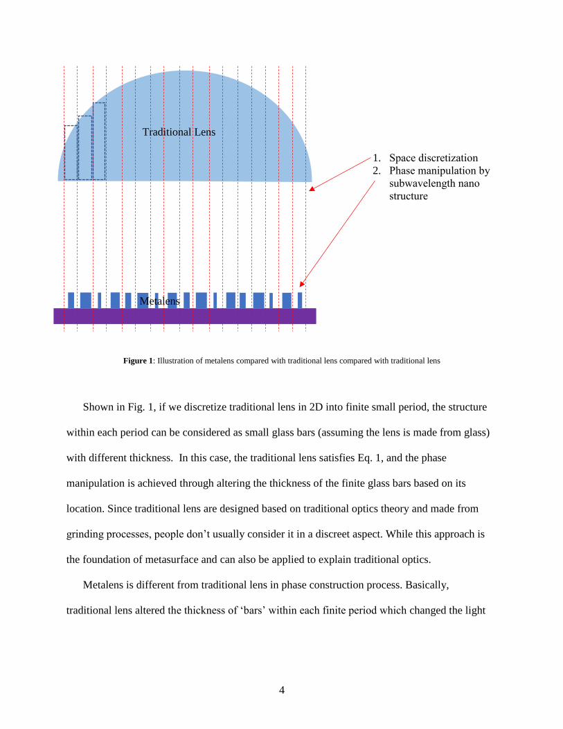
A more vivid way can be applied to better describe metalens as Shown in Figure 1.
4
Shown in Fig. 1, if we discretize traditional lens in 2D into finite small period, the structure
within each period can be considered as small glass bars (assuming the lens is made from glass)
with different thickness. In this case, the traditional lens satisfies Eq. 1, and the phase
manipulation is achieved through altering the thickness of the finite glass bars based on its
location. Since traditional lens are designed based on traditional optics theory and made from
grinding processes, people don’t usually consider it in a discreet aspect. While this approach is
the foundation of metasurface and can also be applied to explain traditional optics.
Metalens is different from traditional lens in phase construction process. Basically,
traditional lens altered the thickness of ‘bars’ within each finite period which changed the light
1. Space discretization
2. Phase manipulation by
subwavelength nano
structure
Traditional Lens
Metalens
Figure 1: Illustration of metalens compared with traditional lens compared with traditional lens
5
propagation length of each ‘finite ray’. In terms of Eq. 1 and 2, the phase required is achieved by
modifying the path length of light propagation.
If we assume a ‘finite ray’ that pass through a media, and this process generate a phase shift
Ø, calculated as:
∅ =𝑛×2𝜋
𝜆× L (3)
Where n is the refractive index of the material within the period, 𝜆 is the wavelength of
electro-magnetic wave, and L is the length of optical path. Basically, traditional lenses achieve
the alteration of phase through changing the ‘L’ term in the discreet finite view.
Metasurface/metalens phase construction is achieved with planar subwavelength nano
structure. Which means the modification of phase is achieved not from the altering the length of
optical path. Instead, propagation-phase based metasurface search for the alteration of effective
index within each finite period, which is the ‘n’ term in Eq. 3.
Refractive index has long been considered as an inherent property of materials. Modification
of materials refractive index can be achieved through altering the composition of material or by
changing the electric/magnetic polarities inside the materials (e.g. ferro-electric or ferro-
magnetic materials. While the design of metasurface is not following either path aforementioned.
The foundation for metasurface phase construction is based on the concept of ‘effective’ index.
As previously mentioned, for metasurface, the surface plane is discretized into finite small
periods. And within each period, we partially fill it with high-refractive-index material. Here we
assume, if the period is small enough, each period can be considered as a complete entity (e.g.
the filled material part and unfilled void together as an entity) with ‘effective’ refractive index.
And the effective index can be adjusted by the filling percentage of high-refractive-index
material. The nano structure within each period (or pitch in 3D) is also known as phase shifter.

6
As a result, the ability of each phase shifter to ‘mimic’ equilibrium media become a key
factor that determines the quality of a metasurface or metalens. Basically, smaller the period is,
better the performance. While the feature size (size of smallest structure) of the metasurface is
limited by current nano fabrication techniques, so the design of metasurface is a trade-off
between optical performance and ease of nano fabrication.
7
Chapter 2 Simulation Method (FDTD and RCWA)
Simulations of optical behaviors are crucial for the design of optical devices. Basically, with the
development of numerical simulation method, we are now able to simulate the physical world
with very high preciseness. In this chapter, I will introduce two major numerical simulation
methods that utilized during the design of optical metasurface.
2.1 Finite Different Time Domain Simulation
Finite-difference time-domain also known as Yee's method (named after the applied
mathematician Kane S. Yee) is a numerical analysis technique used for modeling computational
electrodynamics (finding approximate solutions to the associated system of differential
equations). Since it is a time-domain method, FDTD solutions can cover a wide frequency range
with a single simulation run, and treat nonlinear material properties in a natural way.
The FDTD method belongs in the general class of grid-based differential numerical modeling
methods (finite difference methods). The time-dependent Maxwell's equations (in partial
differential form) are discretized using central-difference approximations to the space and
time partial derivatives. The resulting finite-difference equations are solved in either software or
hardware in a leapfrog manner: the electric field vector components in a volume of space are
solved at a given instant in time; then the magnetic field vector components in the same spatial
8
volume are solved at the next instant in time; and the process is repeated over and over again
until the desired transient or steady-state electromagnetic field behavior is fully evolved.
In this work, the commercial finite difference time domain software Omnisim and Crystal
wave is applied for the field simulation of metasurface. For visible wavelengths, the simulation
grid size is around 3~5 nm which is smaller than one-tenth of the feature size. Sufficiently long
time steps (usually 20000 steps or more based on the size of simulation field) is applied for the
simulation. Perfect matched layer (PML) is applied at all edges of the simulation window to
truncate the simulation area, basically all electronic wave that pass through the edge area are
absorbed. The refractive index of air is set as 1 and the glass as 1.46 at visible range. The
absorption coefficient for dielectric materials are ignored.
2.2 Rigorous Coupled-wave Analysis
Rigorous coupled-wave analysis (RCWA) is a semi-analytical method in computational
electromagnetics that is most typically applied to solve scattering from periodic dielectric
structures. It is a Fourier-space method so devices and fields are represented as a sum of spatial
harmonics. The method is based on Floquet's theorem that the solutions of periodic differential
equations can be expanded with Floquet functions (or sometimes referred as Bloch wave,
especially in solid-state physics community). A device is divided into layers that are each
uniform in the z direction. A staircase approximation is needed for curved devices with
properties such as dielectric permittivity graded along the z-direction. The electromagnetic
modes in each layer are calculated and analytically propagated through the layers. The overall
problem is solved by matching boundary conditions at each of the interfaces between the layers
9
using a technique like scattering matrices. To solve for the electromagnetic modes, which are
decided by the wave vector of the incident plane wave, in periodic dielectric medium,
the Maxwell's equations (in partial differential form) as well as the boundary conditions are
expanded by the Floquet functions and turned into infinitely large algebraic equations. With the
cutting off of higher order Floquet functions, depending on the accuracy and convergence speed
one needs, the infinitely large algebraic equations become finite and thus solvable by computers.
In this study, RCWA method is utilized to calculate phase shifts for single phase shifters.
Although FDTD method can be applied to calculate phase shifts, it requires higher calculation
power that scanning for large dimension scale takes a long time. Here I utilize the RCWA solver
embeded in Omnisim software. Both 2D and 3D RCWA simulation are utilizing periodical
boundary condition, and the phase shift calculation can be achieved within several seconds for
single subwavelength dimention.
10
Chapter 3 Design of Optical Metasurface
Optical metasurface is designed mainly through space discretization and phase reconstruction.
While this process can be divided into several detailed steps as: 1. Space discretization. 2. Filling
material selection. 3. Calculation of discreet phase shifts. 4. Linear regression. 5. Phase matching
and design layout. In this chapter I will discuss these steps in details.
3.1 Space Discretization of Lens Plane
The first step of design a metasurface is space discretization, which basically indicating the
discretization of device plane into finite small grids (periods). There are two factors that
determining the performance of optical metasurface in this step: 1. Size of the grid; 2. Shape of
the grid.
Ideally, the size of the grid should be as small as possible to reduce the influence of space
discretization. While there are several factors that limiting us from idealy-small grid size,
namely, material’s refractive index and nano fabrication capability. Materials with lower
refractive index requires higher thickness to achieve same phase shift (Eq. 3), while this result in
high-aspect-ratio nano structures which increase the fabrication difficulty. In this case, the grid
size is increased to meet minimum fabrication capability. So basically, the size of grid (or
period) is determined by the trade-offs between performance and material-fabrication limitation.
While certain devices have clear upper-limit for the grid size, namely metalens. If a metalens is
11
targeting on diffraction limited focus, its grid size must be smaller than the Abby’s diffraction
limit. While this requirement does not promise high performance metalens. As aforementioned,
ideal phase-reconstruction relies on the mimicking of equilibrium media with designed effective
index. To be specific, for a set of phase shifters, their propagation phase shift should be in near-
linear correlation with the fill-factor within each grid. And usually, the grid size meets this
requirement is smaller than Abby’s diffraction limit.
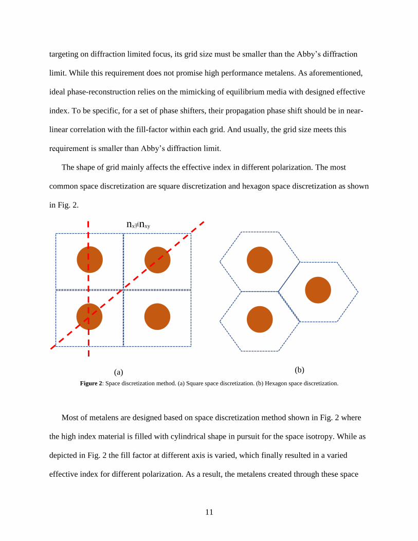
The shape of grid mainly affects the effective index in different polarization. The most
common space discretization are square discretization and hexagon space discretization as shown
in Fig. 2.
Most of metalens are designed based on space discretization method shown in Fig. 2 where
the high index material is filled with cylindrical shape in pursuit for the space isotropy. While as
depicted in Fig. 2 the fill factor at different axis is varied, which finally resulted in a varied
effective index for different polarization. As a result, the metalens created through these space
Figure 2: Space discretization method. (a) Square space discretization. (b) Hexagon space discretization.
(a) (b)
nx≠nxy
12
discretization methods are called ‘polarization insensitive’. There are also pure isotropic design,
which end up with a grating based metalens, which will be discussed in later chapters.
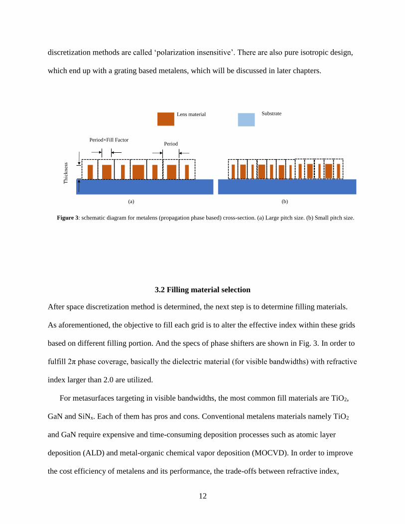
3.2 Filling material selection
After space discretization method is determined, the next step is to determine filling materials.
As aforementioned, the objective to fill each grid is to alter the effective index within these grids
based on different filling portion. And the specs of phase shifters are shown in Fig. 3. In order to
fulfill 2π phase coverage, basically the dielectric material (for visible bandwidths) with refractive
index larger than 2.0 are utilized.
For metasurfaces targeting in visible bandwidths, the most common fill materials are TiO2,
GaN and SiNx. Each of them has pros and cons. Conventional metalens materials namely TiO2
and GaN require expensive and time-consuming deposition processes such as atomic layer
deposition (ALD) and metal-organic chemical vapor deposition (MOCVD). In order to improve
the cost efficiency of metalens and its performance, the trade-offs between refractive index,
(a) (b)
Lens material Substrate
Period×Fill Factor Period
Figure 3: schematic diagram for metalens (propagation phase based) cross-section. (a) Large pitch size. (b) Small pitch size.
13
fabrication difficulty and metalens performance is studied in later chapter. And we have
developed a feasible approach that is silicon-rich nitride (SiNx) as metalens material, which
balance the trade-offs between refractive index and fabrication difficulty to large extent.
3.3 Calculation of discreet phase shift
In order to acquire a proper set of phase shifter (continuously shifting phase through 0-2π),
researchers have to search large material-dimension combinations. This process can be achieved
through RCWA calculation. One thing to be noted is that when calculating the phase shift of a
single dimension, we consider a periodical boundary condition. While during the phase
reconstruction of metalens process, these phase shifters are placed based on the phase matching
equation. To be specific, a metasurface is rarely designed to be a periodic structure. So there are
always possibility that unpredicted resonance or scatter occur at adjacent phase shifter area.
3.4 linear regression, phase matching and design layout
After a set of phase shifter is acquired, we basically have a number of periods, fill factors related
phase shift. A common step I utilize before phase matching is linear regression of these points
which end up with a dimension-phase shift function, which is continuous.
As aforementioned, the design of metasurface generate a space-variant phase profile (Eq. 1,
2). In order to lay out the surface design, we have to generate a space-variant dimension profile,

14
which is acquired by combining the dimension-phase shift function with the space-variant phase
profile.
Additionally, metasurface usually requires numerous of phase shifters, the 3D layout of
metasurface thus requires programming-based method. In this study, the 3D layout of metalens
structure is achieved through Matlab and Python programming, example code is attached in
appendix.
15
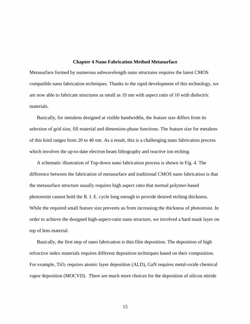
Chapter 4 Nano Fabrication Method Metasurface
Metasurface formed by numerous subwavelength nano structures requires the latest CMOS
compatible nano fabrication techniques. Thanks to the rapid development of this technology, we
are now able to fabricate structures as small as 10 nm with aspect ratio of 10 with dielectric
materials.
Basically, for metalens designed at visible bandwidths, the feature size differs from its
selection of grid size, fill material and dimension-phase functions. The feature size for metalens
of this kind ranges from 20 to 40 nm. As a result, this is a challenging nano fabrication process
which involves the up-to-date electron beam lithography and reactive ion etching.
A schematic illustration of Top-down nano fabrication process is shown in Fig. 4. The
difference between the fabrication of metasurface and traditional CMOS nano fabrication is that
the metasurface structure usually requires high aspect ratio that normal polymer-based
photoresist cannot hold the R. I. E. cycle long enough to provide desired etching thickness.
While the required small feature size prevents us from increasing the thickness of photoresist. In
order to achieve the designed high-aspect-ratio nano structure, we involved a hard mask layer on
top of lens material.
Basically, the first step of nano fabrication is thin film deposition. The deposition of high
refractive index materials requires different deposition techniques based on their composition.
For example, TiO2 requires atomic layer deposition (ALD), GaN requires metal-oxide chemical
vapor deposition (MOCVD). There are much more choices for the deposition of silicon nitride
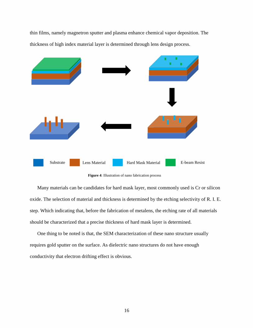
16
thin films, namely magnetron sputter and plasma enhance chemical vapor deposition. The
thickness of high index material layer is determined through lens design process.
Many materials can be candidates for hard mask layer, most commonly used is Cr or silicon
oxide. The selection of material and thickness is determined by the etching selectivity of R. I. E.
step. Which indicating that, before the fabrication of metalens, the etching rate of all materials
should be characterized that a precise thickness of hard mask layer is determined.
One thing to be noted is that, the SEM characterization of these nano structure usually
requires gold sputter on the surface. As dielectric nano structures do not have enough
conductivity that electron drifting effect is obvious.
Substrate Lens Material Hard Mask Material E-beam Resist
Figure 4: Illustration of nano fabrication process
17
Chapter 5 Silicon-rich Silicon Nitride Thin Films for Metalens
The engineering of phase shift through nano structures is the most important process for the
design of metalens. In order to achieve the phase profile aforementioned through propagation
phase, the lens plane is first discretized into finite number of pitches (period). Then high-
refractive index materials are filled into each pitch with designed geometry, which provide
variation of effective index over the lens plane. The objective of this step is to achieve the
engineering of optical response within each period including transmission and phase shift.
In order to achieve 2π propagation-phase coverage (distinguishing from Pancharatnam-Berry
phase), high-refractive index materials such as TiO2 [3] and GaN [8] are applied. In most cases,
the highest aspect ratio of nanostructures fabricated is around 10 to ensure precise phase
coverage. While the application of TiO2 and GaN as lens material involves atomic layer
deposition (ALD) or metal-organic chemical vapor deposition (MOCVD). This has increased the
time and cost of metalens fabrication to a large extent.
The most important approach to improve the performance of metalens is to shrink the pitch
size (also known as period). In this way, researchers are trying to avoid the influence on
wavefront caused by the discretization of space, so that the loss caused by scattering or unwanted
resonance is minimized. While the decrease of pitch size (period) in pursuit of higher focus
efficiency is limited by nano fabrication, to be specific, the minimum physical dimension of a
phase shifter is limited. As a result, there exist a fabrication-limited minimum pitch size for
certain material and incident wavelength combination to achieve 2π propagation-phase coverage.
18
In this work, we have developed silicon rich silicon nitride (SiNx) as metalens material with a
more cost-efficient thin film deposition process: physical vapor deposition (PVD) and plasma
enhanced vapor deposition (PECVD). We have achieved a film with much higher refractive
index n=2.74 at targeting wavelength 685 nm which enabled unprecedented small pitch size of
220 nm. A subwavelength grating metalens with 220 nm pitch size under 685 nm light is
designed, fabricated and characterized in this work.
5.1 Development of high-refractive-index silicon rich silicon nitride (SiNx) films for
metalens design
Silicon nitride is a conventional material applied in CMOS industry as passivation layer. Recent
advances in optical communication have seen the application of Si3N4 as ultra-low loss
waveguide [12].
For the metalens application, Si3N4 with refractive index around 2.0 in visible bandwidth
requires nano structures with high thickness for the coverage of 2π phase. Limited by current
nano fabrication techniques, this has result in a large pitch size [13]. In this case, the negative
impact of space discretization on focus efficiency is inevitable. The common upper limit for
pitch size is below the Abby’s diffraction limit (𝜆
2𝑁𝐴), if the lens is designed for the diffraction
limited focus. In order to achieve small pitch size with 2π coverage, lens material with a higher
index seems required.
Common deposition of Si3N4 thin films are basically vapor deposition processes namely
PVD and PECVD. Recent studies have reported adjustment of optical parameters of SiNx (x as
19
variable) films through both approaches [14-15], but a high refractive index SiNx film suitable
for metalens application has not yet been developed.
5.1.1 Silicon rich silicon nitride film deposited by magnetron sputter
Conventional physical vapor deposition (PVD) of silicon nitride thin film is through magnetron
sputtering of pure Si3N4 target. In order to increase the refractive index of silicon nitride, the
concentration of silicon is supposed to be increased. And this result in a silicon rich silicon
nitride material.
In this study, we have developed a reactive magnetron sputtering process for high-refractive-
index SiNx thin films. A silicon target (Kurt J. Lesker) is applied on direct current source (DC)
of PVD 75 magnetron sputtering tool (Kurt J. Lesker). The DC power is fixed at 350 W. A radio-
frequency bias power is applied on the substrate at 60 W. The pressure of process chamber is
fixed at 6 mT with N2 and Ar gas flow simultaneously. The gas contration N2/Ar is varied from
10% to 20%. All films are deposited with thickness around 200 nm and their optical parameters
(n & k) is measured through ellipsometer (Woollam). The result of n & k is shown in Fig. 5.
20
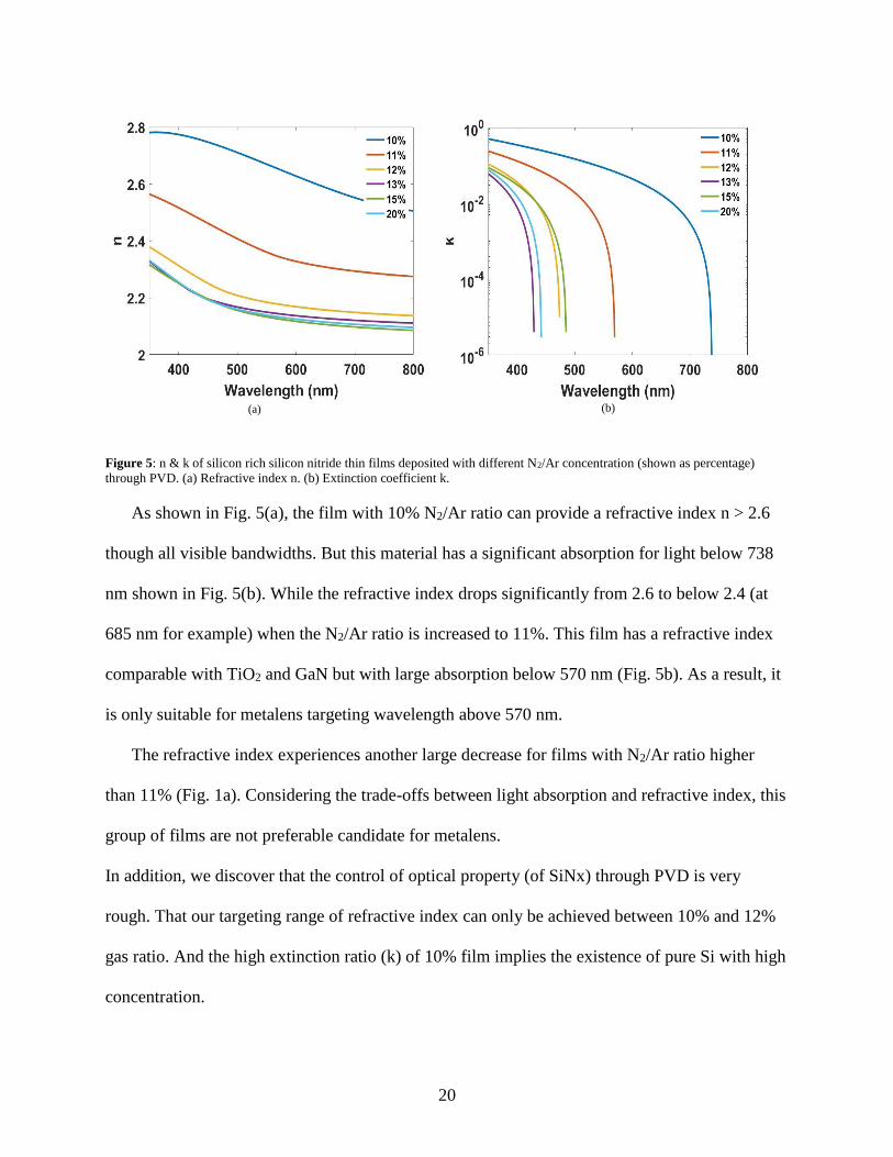
Figure 5: n & k of silicon rich silicon nitride thin films deposited with different N2/Ar concentration (shown as percentage)
through PVD. (a) Refractive index n. (b) Extinction coefficient k.
As shown in Fig. 5(a), the film with 10% N2/Ar ratio can provide a refractive index n > 2.6
though all visible bandwidths. But this material has a significant absorption for light below 738
nm shown in Fig. 5(b). While the refractive index drops significantly from 2.6 to below 2.4 (at
685 nm for example) when the N2/Ar ratio is increased to 11%. This film has a refractive index
comparable with TiO2 and GaN but with large absorption below 570 nm (Fig. 5b). As a result, it
is only suitable for metalens targeting wavelength above 570 nm.
The refractive index experiences another large decrease for films with N2/Ar ratio higher
than 11% (Fig. 1a). Considering the trade-offs between light absorption and refractive index, this
group of films are not preferable candidate for metalens.
In addition, we discover that the control of optical property (of SiNx) through PVD is very
rough. That our targeting range of refractive index can only be achieved between 10% and 12%
gas ratio. And the high extinction ratio (k) of 10% film implies the existence of pure Si with high
concentration.
(a) (b)
21
5.1.2 Silicon rich silicon nitride film deposited by plasma enhanced chemical vapor
deposition
Plasma enhanced chemical vapor deposition (PECVD) has long been a reliable approach for the
deposition of Si3N4. In this study we have applied SiH4 and NH3 as reaction gas for the
deposition of SiNx under 350 °C. The refractive index of film is tuned by the variation of gas
concentration. The pressure is fixed at 2 torr. The optical parameters (n & k) of deposited films
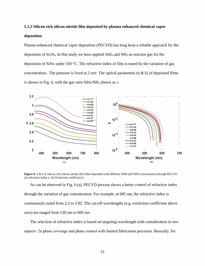
is shown in Fig. 6, with the gas ratio SiH4/NH3 shown as α.
Figure 6: n & k of silicon rich silicon nitride thin films deposited with different SiH4 and NH3 concentration through PECVD.
(a) refractive index n. (b) Extinction coefficient k.
As can be observed in Fig. 6 (a), PECVD process shows a better control of refractive index
through the variation of gas concentration. For example, at 685 nm, the refractive index is
continuously tuned from 2.2 to 2.82. The cut-off wavelengths (e.g. extinction coefficient above
zero) are ranged from 530 nm to 600 nm.
The selection of refractive index is based on targeting wavelength with consideration in two
aspects: 2π phase coverage and phase control with limited fabrication precision. Basically, for
(a) (b)
22
phase shifters, high refractive index lowered the aspect-ratio needed for 2π coverage. While it
increases the requirement of fabrication precision for phase control. And this PECVD process
with continuous tuning of refractive index provides unprecedented balancing of these 2 factors
based on targeting wavelengths.
Considering aforementioned trade-offs, the film deposited with SiH4/NH3 ratio 4.68 with
high refractive-index (n = 2.74 at 685 nm) and k = 0 above 600 nm is preferable for metalens
targeting beyond 600 nm bandwidths. And we have chosen this film for later design.
5.2 Shrinking the pitch size of metalens with high index SiNx material
The major approach to increase the efficiency of metalens is to minimize the influence cause by
space discretization. This method, in other words, is to shrink the pitch size (period) of each
phase shifter. A schematic diagram of propagation-phase-based metalens in 2-D is shown in Fig.
3, with large pitch size (Fig. 3a) and small pitch size (Fig. 3b). And the smallest reachable pitch
size is limited by feature size (e.g. smallest nano structure) of nano fabrication. The structure
within each pitch (period) is defined by the fill factor and thickness. Fill factor represents the
percentage of period (e.g. length in 2D and area in 3D) filled by lens material. Theoretically, the
phase coverage is increased with the increase of lens material’s refractive index and the thickness
of phase shifter. Based on current fabrication techniques, the dimension of phase shifters is
limited to certain feature size and thickness combination (e.g. maximum-achievable aspect ratio).
As a result, the pitch size for conventional TiO2 based metalens is 350 nm with the thickness of
600 nm under 660 nm light [16]. This pitch size is near the limit (e.g. near the smallest-possible
pitch size) for material with n = 2.4 to cover 2 π phase shift.
23
In this study we are able to shrink the pitch size down to 220 nm under 685 nm light with silicon-
rich silicon nitride developed. The phase distribution for phase shifters under 220 nm pitch with
n =2.74 and n = 2.4 is calculated through RCWA (Photon Design Ltd.) and is shown in Fig. 7
(a). Both phase shifters are 600 nm thick with feature size of 60 nm, which indicating a
fabrication-limited aspect ratio 10:1. As shown in Fig. 4(a), n = 2.74 can achieve a continuous
full phase coverage under the fabrication-limited features while n = 2.4 material can only cover
half of it.
In order to evaluate the effectiveness of minimization of space discretization on focus
efficiency, a series of propagation-phase-based metalens are designed in 2D with pitch size
(period) ranging from 220 nm to 360 nm. These lenses are designed with high numerical aperture
NA = 0.9 under incidence of 685 nm light. The thickness of the lens is fixed at 600 nm and the
feature size is set around 60 nm. FDTD simulation is performed for all lenses under appropriate
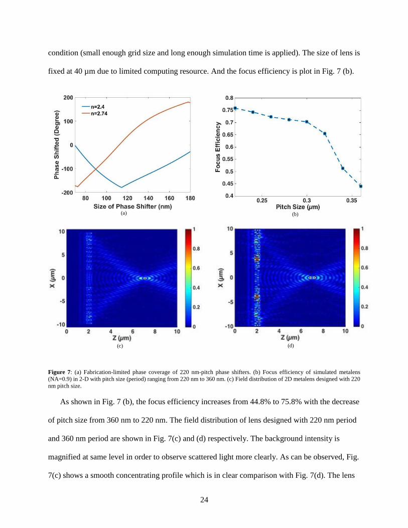
24
condition (small enough grid size and long enough simulation time is applied). The size of lens is
fixed at 40 µm due to limited computing resource. And the focus efficiency is plot in Fig. 7 (b).
Figure 7: (a) Fabrication-limited phase coverage of 220 nm-pitch phase shifters. (b) Focus efficiency of simulated metalens
(NA=0.9) in 2-D with pitch size (period) ranging from 220 nm to 360 nm. (c) Field distribution of 2D metalens designed with 220
nm pitch size.
As shown in Fig. 7 (b), the focus efficiency increases from 44.8% to 75.8% with the decrease
of pitch size from 360 nm to 220 nm. The field distribution of lens designed with 220 nm period
and 360 nm period are shown in Fig. 7(c) and (d) respectively. The background intensity is
magnified at same level in order to observe scattered light more clearly. As can be observed, Fig.
7(c) shows a smooth concentrating profile which is in clear comparison with Fig. 7(d). The lens
(b)
(c) (d)
(a)
25
designed with 360 nm pitch size shows strong resonance behavior at lens plane compared with
220 nm pitched lens. And the scattered light outside the focusing profile is notable in Fig. 7(d).
This decrease of focusing performance of 360 nm pitched lens (compared with 220 nm lens) is a
result of coarse space discretization. In this case, scattering and undesired resonance become
more significant.
5.3 Lens fabrication and characterization
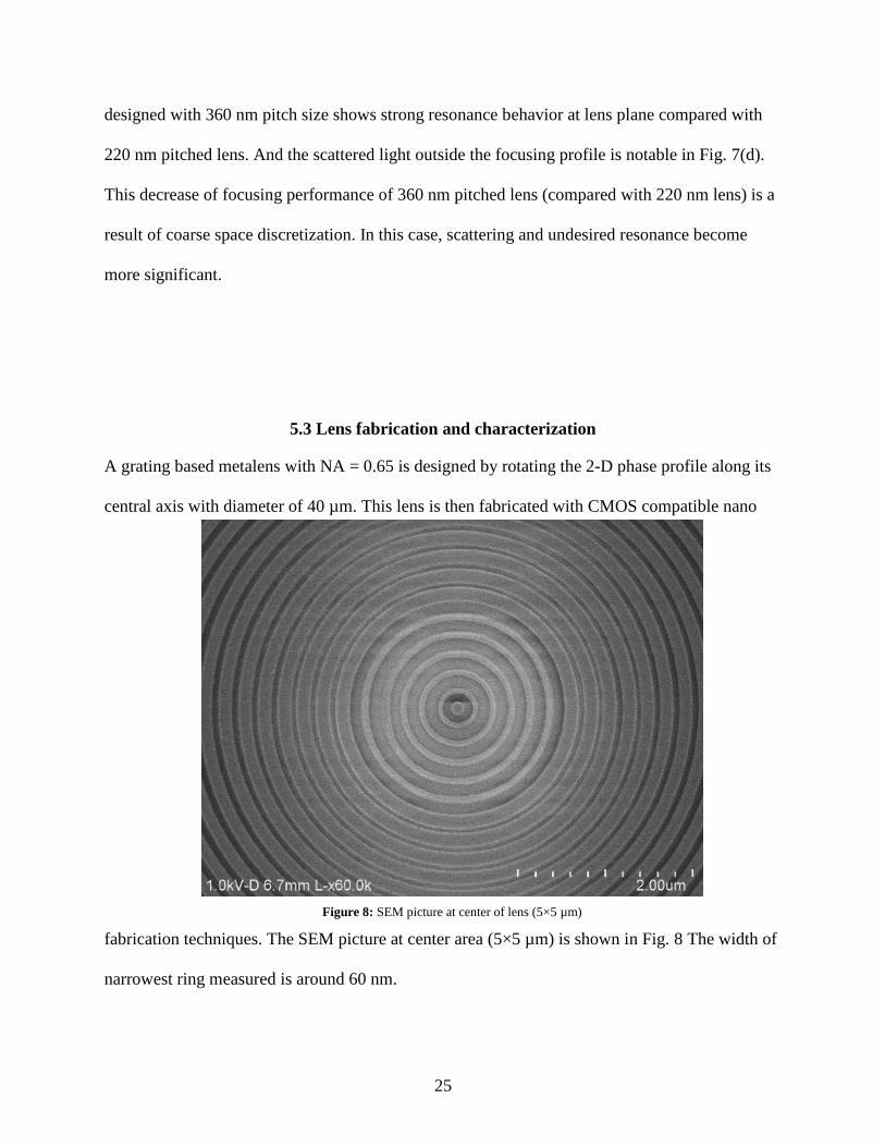
A grating based metalens with NA = 0.65 is designed by rotating the 2-D phase profile along its
central axis with diameter of 40 µm. This lens is then fabricated with CMOS compatible nano
fabrication techniques. The SEM picture at center area (5×5 µm) is shown in Fig. 8 The width of
narrowest ring measured is around 60 nm.
Figure 8: SEM picture at center of lens (5×5 µm)
26
The silicon rich silicon nitride (SiNx, n = 2.74) layer with thickness of 600 nm is deposited
on the substrate of glass wafer as lens material. Then a 300 nm thick SiO2 layer is deposited on
top of SiNx layer as a hard mask. Before E-beam lithography, a photoresist layer (ZEP520A) of
200 nm is spin coated on top of SiO2 layer. The 2-D lens pattern is written by E-beam and the
pattern is created on the photoresist after development. The lens structure is then transferred into
SiO2 hard mask layer by reactive ion etching (R.I.E.) and the residual photoresist is stripped by
O2 plasma stripper. The pattern is finally transferred into silicon rich silicon nitride layer by
another reactive ion etching process. The selectivity of SiNx/SiO2 is around 2.0 with the
application of 20% of SF6 concentration during reactive ion etching.
The reason for our utilization of SiO2 layer as hard mask is because there is no E-beam
photoresist available (at 200 nm thickness) to provide enough selectivity versus SiNx to achieve
direct R.I.E. with 600 nm depth. While the thickness of E-beam resist is limited by the feature
size around 60 nm. As a result, a two-step R.I.E. process with hard mask is necessary for the
fabrication of this metalens.
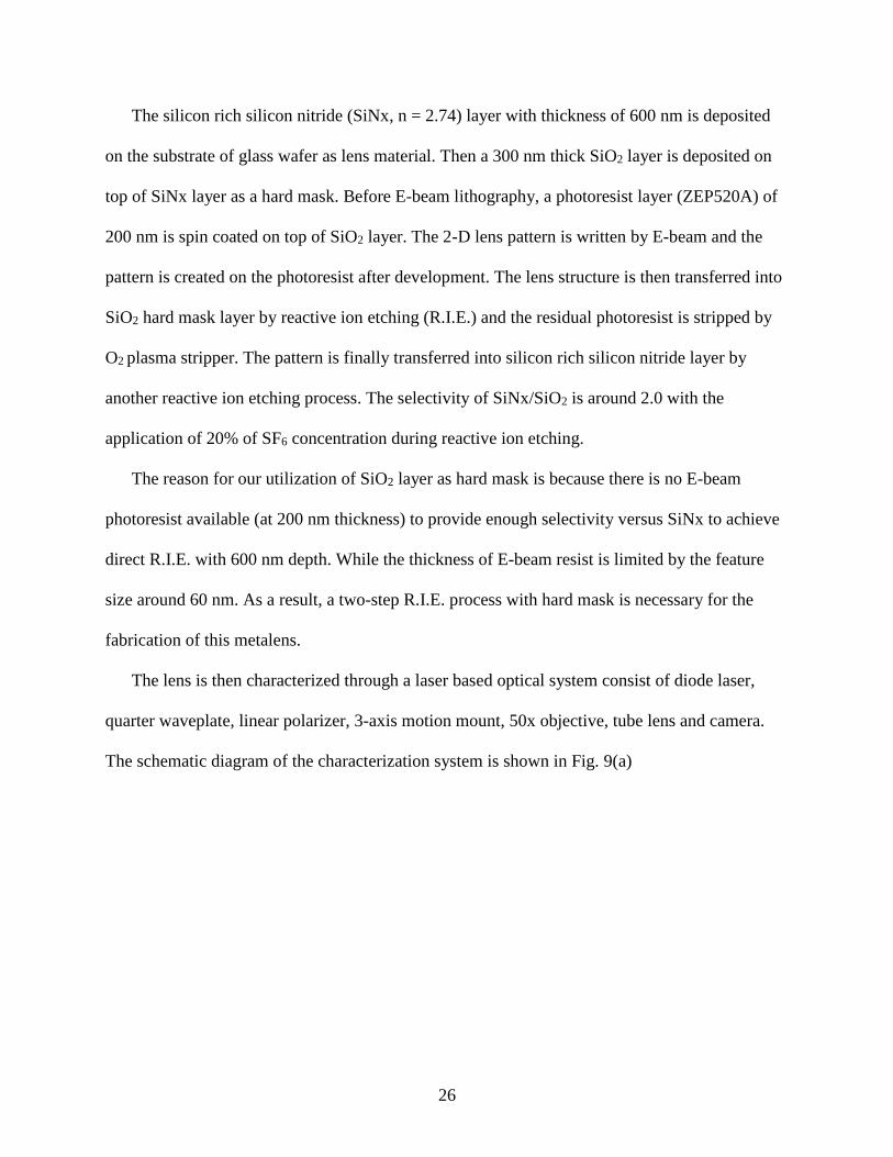
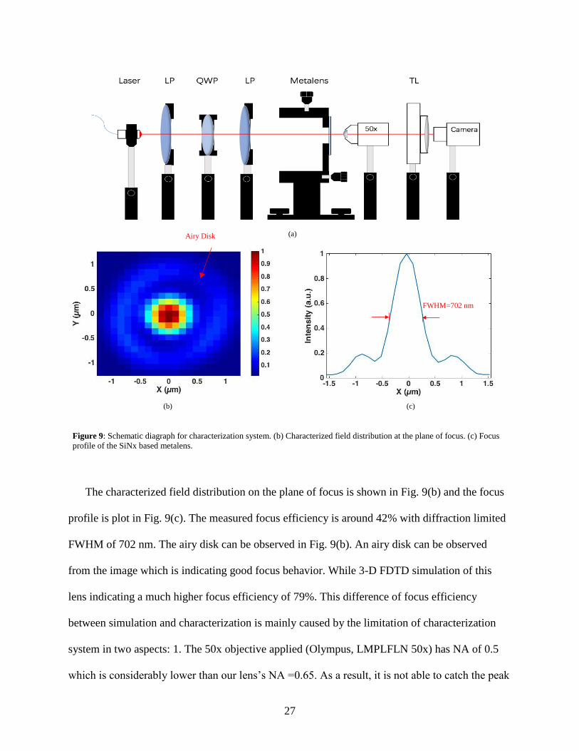
The lens is then characterized through a laser based optical system consist of diode laser,
quarter waveplate, linear polarizer, 3-axis motion mount, 50x objective, tube lens and camera.
The schematic diagram of the characterization system is shown in Fig. 9(a)
27
The characterized field distribution on the plane of focus is shown in Fig. 9(b) and the focus
profile is plot in Fig. 9(c). The measured focus efficiency is around 42% with diffraction limited
FWHM of 702 nm. The airy disk can be observed in Fig. 9(b). An airy disk can be observed
from the image which is indicating good focus behavior. While 3-D FDTD simulation of this
lens indicating a much higher focus efficiency of 79%. This difference of focus efficiency
between simulation and characterization is mainly caused by the limitation of characterization
system in two aspects: 1. The 50x objective applied (Olympus, LMPLFLN 50x) has NA of 0.5
which is considerably lower than our lens’s NA =0.65. As a result, it is not able to catch the peak
(a)
(b) (c)
FWHM=702 nm
Airy Disk
Figure 9: Schematic diagraph for characterization system. (b) Characterized field distribution at the plane of focus. (c) Focus
profile of the SiNx based metalens.
28
intensity of diffraction limited focus. 2. The resolution for motion system (Thorlabs, MT3A) is
0.5 µm, which is similar to the size of diffraction limited focus (532 nm). In this case, the capture
of exact focal plane become extremely challenging.
5.4 Discussion
Emerging metalens is designed based on the discretization of space into finite number of pitches
(periods) and the application of high-refractive index materials. While traditional metalens
material such as TiO2 or GaN involves expensive and time-consuming deposition process. In
addition, further shrinking of pitch size in pursuit of better performance is restricted by nano
fabrication limitation and material’s refractive index.
In this study, we have developed a more cost-effective CMOS compatible silicon rich silicon
nitride material for metalens fabrication with considerably higher refractive index. The pitch size
of propagation-phase-based metalens can be shrinked to unprecedented 220 nm for the incidence
of 685 nm light. A subwavelength grating metalens is designed and characterized for the prove
of concept. The feature size and aspect ratio of the 220 nm pithed metalens demonstrated are
similar to conventional TiO2 350 nm pitched metalens. This is enabled by the development of
ultra-high refractive index SiNx thin film (n = 2.74) at 685 nm incidence.
The major drawback of this silicon rich silicon nitride material is the absorption under certain
visible wavelength. As a result, it is not preferable for the design of achromatic metalens. On the
other hand, this special dispersion relationship provides the integration of metalens with long-
pass filter. In addition, with the continuous tunability of refractive index through PECVD, silicon

29
rich silicon nitride films provide a new degree of freedom for the modification of phase through
artificial phase shifters.
30
Chapter 6 Linear Polarization Distinguishing Metalens in Visible Wavelength
Traditional control of polarization is basically achieved through optical devices namely, polarizer
and wave plate. Linear polarizer allows the propagation of certain linearly polarized electro-
magnetic wave while prohibits its orthogonal polarization by either absorption or redirection
(through birefringent effect). Wave plate is a typical application of a group of birefringent
materials. Upon the propagation of electromagnetic wave through the wave plate, a designed
phase difference is created between orthogonal optical axis, which changes the polarization state
of the propagated electro-magnetic wave. With the development of optical metasurface,
researchers are able to create subwavelength birefringence unit in nano scale [17]. This has led
to the design and fabrication of metalens utilizing Pancharatnam-Berry phase (also known as
geometric phase) based on circularly polarized incidence. The basic structures (phase shifters) of
these metalens are (in most cases) a group of cuboids with space-variant orientation. These phase
shifters can also be considered as small waveplates. By tuning the orientation of these tinny
waveplates, researchers are able to acquire 2π phase shift coverage which is essential for lens
design. In addition, it is possible to distinguish circular polarization state (e.g. left-handed
circular polarization, LCP and right-handed circular polarization, RCP) by applying two sets of
phase shifters in one lens [18], which results in a hybrid metalens that creates different focus or
image with the incidence of LCP or RCP light. Even though linearly polarized light can be
viewed as the superposition of left-handed and right-handed circularly polarized light, it is not
efficient to design the metalens for linearly polarized incidence with Pancharatnam-Berry phase
shifters, as Berry-phase shifters only works under certain polarization (e.g. either LCP or RCP).
31
In order to achieve metalens for linearly polarized incidence, researchers have looked into the
modification of propagation phase. This modification is usually achieved by altering the size of
nano structure (e.g. period and fill factor) at sub-wavelength scale that the phase shifted (e.g.
phase shift of the 0th diffraction mode) upon propagation is altered. With the help of modern
computer aided engineering tool (e.g. FDTD and RCWA), people are able to acquire the phase
shift for a number of nano structures with various of dimensions and materials in a convenient
way. The metalens for linear polarized incidence is then formed by a group of nano structures
with space-variant dimensions with designed space-variant phase shift. These phase shifters are
usually appeared as cylinders with space-variant diameters [19-20] and are considered as
polarization-intensitive.
In this study, we have designed, fabricated and characterized a linear polarization
distinguishing metalens by increasing the polarization sensitivity of individual phase shifters,
while maintaining necessary phase coverage on the designed polarization. The linear polarization
distinguishing performance of this metalens is confirmed by both simulation and optical
characterization. It is the first focusing metalens designed with a linear polarization
distinguishing focus.
Metalens is physically formed by a number of subwavelength nano structures which are also
known as phase shifters. The dimension of individual phase shifters is altered based on its
location to form a space-variant phase profile. The phase profile of concentrating metalens in x-z
plane is shown as equation 5.
ϕ(x, z) − ϕ(0,0) =2𝜋
𝜆(√𝑥2 + 𝑧2 + 𝑓2 − 𝑓) = −Δϕ(x, z) (5)
Where 𝜆 is the incident wavelength, x and z are the space coordinate (assuming the center is
0,0). Ф(x, z) is the phase needed at (x, z) location and ∆Ф (x, z) is the phase shift of the nano
32
structure at this location. In this equation, the lens is laid out at x-z plane and the light is incident
in y direction. The focus is formed at the center of the focal plane with a distance of 𝑓 (focal
length) to the lens plane.
For metalens designed under linear polarized incidence, the control of phase is achieved by
the variation of nano structure at the lens plane (e.g. the variation of period and fill factor). At 3-
D domain, conventional phase shifters for concentrating metalens are mostly cylinder nano
structures confined within individual period shaped by square [19] (Fig. 10 a) or hexagon [20].
In other words, their 2-D lens plane is discretized into finite number of squares or haxagons. In
this case, the phase variation is achieved by tuning the diameter of cylinder nano structure (e.g.
the effective index is varied within the period). While this design is polarization-intensitive,
because for each phase shifter, the variation of effective index with the change of incident
polarization is negligible [19]. Another example of polarization intensitive metalens is the
grating metalens. By rotating the 2-D space-variant dimension profile along the central axis,
metalens can be designed with concentric rings structure [3, 20] and this design is purely
isotropic.
33
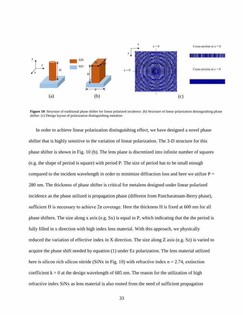
In order to achieve linear polarization distinguishing effect, we have designed a novel phase
shifter that is highly sensitive to the variation of linear polarization. The 3-D structure for this
phase shifter is shown in Fig. 10 (b). The lens plane is discretized into infinite number of squares
(e.g. the shape of period is square) with period P. The size of period has to be small enough
compared to the incident wavelength in order to minimize diffraction loss and here we utilize P =
280 nm. The thickness of phase shifter is critical for metalens designed under linear polarized
incidence as the phase utilized is propagation phase (different from Pancharatnam-Berry phase),
sufficient H is necessary to achieve 2π coverage. Here the thickness H is fixed at 600 nm for all
phase shifters. The size along x axis (e.g. Sx) is equal to P, which indicating that the the period is
fully filled in x direction with high index lens material. With this approach, we physically
reduced the variation of effective index in X direction. The size along Z axis (e.g. Sz) is varied to
acquire the phase shift needed by equation (1) under Ez polarization. The lens material utilized
here is silicon rich silicon nitride (SiNx in Fig. 10) with refractive index n = 2.74, extinction
coefficient k = 0 at the design wavelength of 685 nm. The reason for the utilization of high
refractive index SiNx as lens material is also rooted from the need of sufficient propagation
z
x
y
(a) (b) (c)
Cross-section at x = 0
Cross-section at z = 0
z
x
x = 0
z = 0
Sz
H
H
P
SiN
SiO
Figure 10: Structure of traditional phase shifter for linear polarized incidence. (b) Structure of linear polarization distinguishing phase
shifter. (c) Design layout of polarization distinguishing metalens
34
phase shift within small period. The lens is designed on glass wafer with n = 1.46 and thickness
of 500 µm. The optical properties of glass wafer and SiNx films are measured through woollam
M-2000 ellipsometer. By matching the phase requirement in equation (1), a polarization
distinguishing lens is designed and shown in Fig. 10 (c) with top view and cross section views
(light is incidented in Y direction).
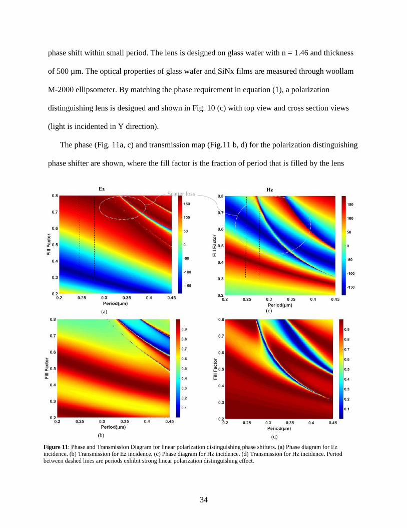
The phase (Fig. 11a, c) and transmission map (Fig.11 b, d) for the polarization distinguishing
phase shifter are shown, where the fill factor is the fraction of period that is filled by the lens
(c)
(d)
(a)
(b)
Scatter loss Ez Hz
Figure 11: Phase and Transmission Diagram for linear polarization distinguishing phase shifters. (a) Phase diagram for Ez
incidence. (b) Transmission for Ez incidence. (c) Phase diagram for Hz incidence. (d) Transmission for Hz incidence. Period
between dashed lines are periods exhibit strong linear polarization distinguishing effect.
35
material (Sz = Period × Fill Factor). These phase and transmission map is calculated through
rigorous coupled wave analysis (RCWA, Photon Design Ltd.) with wavelength of 685 nm. As
can be observed from Fig. 11 (a), from period 0.3-0.45 µm, a continuous variation of phase shift
is not accompanied with the constant change of fill factor, which is indicating the existence of
scattering loss. To be specific, each individual period that forms metalens/metasurface is
mimicking a homogenous medium with different effective index. In this case, the effective index
is tuned by the fill factor, so ideally, the phase shifted is supposed to be in positive correlation
with fill factor. The existence of abrupt phase shift shows the formation of strong resonance
(c) (d)
Ez incidence Hz incidence
Ez incidence Hz incidence
(a) (b)
Figure 12: Field distribution at cross-section x=0 of the lens at Ez and Hz incidence. (a) Field distribution under incidence of Ez
Polarization. (b) Field distribution under incidence of Hz polarization. Lens plane is marked as red line. (c) Field distribution of lens when Ez is incident. (d) Field distribution of lens when Hz is incident. Lens structures are confined within red dash line. Lens structures are within the area marked by red dash lines.
36
within the structure that cause scattering loss to the lens. As a result, the upper limit for period
for the lens design is set to 0.3 µm.
In order to achieve linear polarization distinguishing at Ez polarization, it is important to
reduce its performance under Hz. This can be achieved through two approaches. The first one is
to reduce the phase coverage under the incidence of Hz while maintain 2π coverage under Ez. As
calculated from Fig. 11 (a) and (c), at 0.22<P<0.3 µm, there exists 2π phase coverage (e.g. when
fill factor is varied) under Ez. While its phase covered under Hz varies from 1.2π to 1.33π, which
does not show significant improvement. The other approach is to create scattering loss at
unwanted incident polarization. As aforementioned, each period inside metalens/metasurface is
mimicking a homogeneous medium with effective index tuned by fill factor. Failure of
continuous tuning of phase shift by constant change of fill factor is indicating strong scattering or
unwanted resonance, which can be observed in Fig. 11 (c) at 0.26<P<0.3 µm area (between
dashed lines). This means phase shifters designed within this area experience strong scattering
loss under Hz polarized incidence while remains stable tuning of phase under Ez polarized
incidence, which is the property of our interest.
Even though smaller period generally indicating better lens performance, the lower limit of P
is restricted by current nano fabrication technology as the fabrication of small nano structure
with high aspect ratio is very challenging (in this case H = 600 nm) either by deep reactive ion
etching (DRIE) or lift-off process [14]. By considering the trade-off between performance and
fabrication, we finally pick P = 280 nm and designed a 10×10 µm polarization distinguishing
lens with numerical aperture NA = 0.9 for the proof of concept simulation. The smallest feature
in this lens is around 48 nm.
37
The performance of this lens is then simulated by 3-D finite difference time domain (FDTD)
method (Omnisim, Photon Design Ltd.). Perfect match layer (PML) is applied on all boundaries
of simulation window to truncate simulation space. Refractive index of SiO2 substrate and air are
1.46 and 1 respectively. Imaginary part of refractive index for glass and air are set zero,
sufficient small grid size and sufficient long simulation times are applied for the simulation.
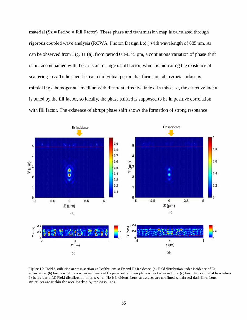
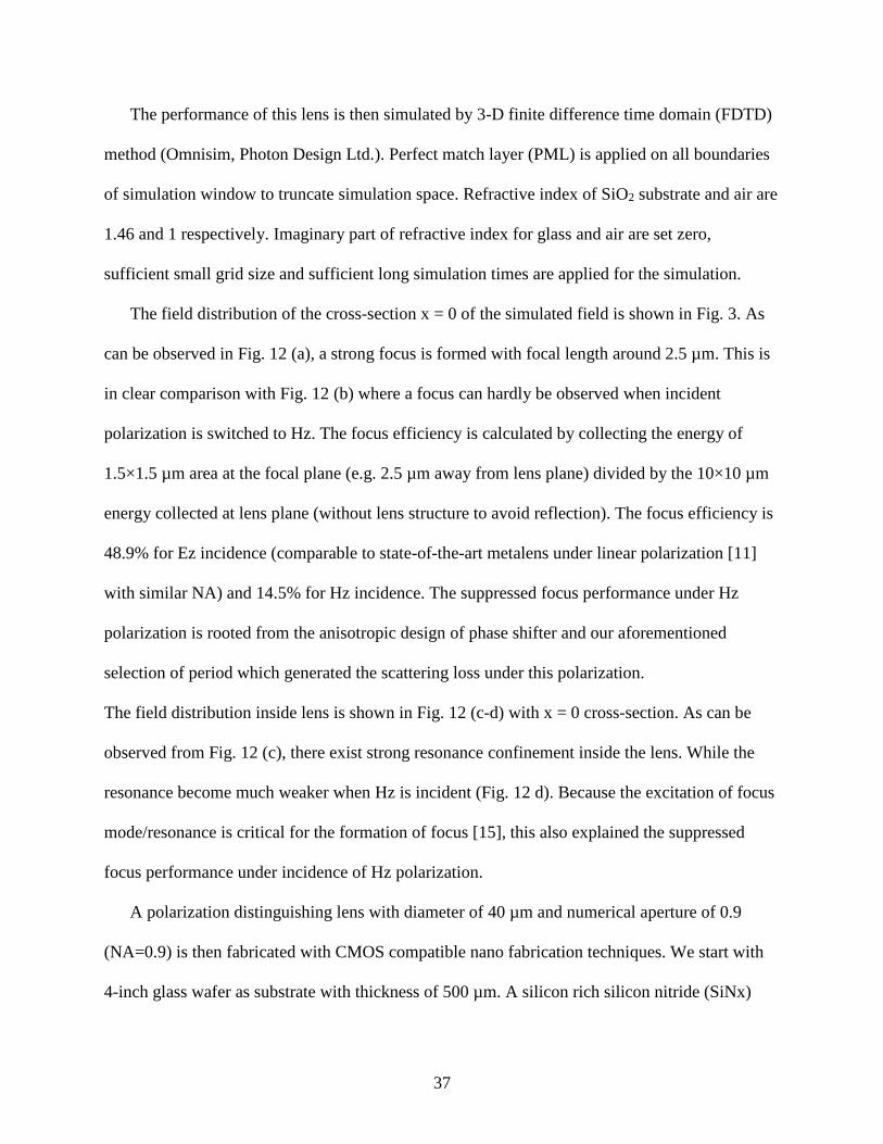
The field distribution of the cross-section x = 0 of the simulated field is shown in Fig. 3. As
can be observed in Fig. 12 (a), a strong focus is formed with focal length around 2.5 µm. This is
in clear comparison with Fig. 12 (b) where a focus can hardly be observed when incident
polarization is switched to Hz. The focus efficiency is calculated by collecting the energy of
1.5×1.5 µm area at the focal plane (e.g. 2.5 µm away from lens plane) divided by the 10×10 µm
energy collected at lens plane (without lens structure to avoid reflection). The focus efficiency is
48.9% for Ez incidence (comparable to state-of-the-art metalens under linear polarization [11]
with similar NA) and 14.5% for Hz incidence. The suppressed focus performance under Hz
polarization is rooted from the anisotropic design of phase shifter and our aforementioned
selection of period which generated the scattering loss under this polarization.
The field distribution inside lens is shown in Fig. 12 (c-d) with x = 0 cross-section. As can be
observed from Fig. 12 (c), there exist strong resonance confinement inside the lens. While the
resonance become much weaker when Hz is incident (Fig. 12 d). Because the excitation of focus
mode/resonance is critical for the formation of focus [15], this also explained the suppressed
focus performance under incidence of Hz polarization.
A polarization distinguishing lens with diameter of 40 µm and numerical aperture of 0.9
(NA=0.9) is then fabricated with CMOS compatible nano fabrication techniques. We start with
4-inch glass wafer as substrate with thickness of 500 µm. A silicon rich silicon nitride (SiNx)
38
layer with thickness of 600 nm is deposited on the substrate as lens material. Then a silicon
dioxide layer with thickness of 300 nm is then deposited on top of SiNx layer as a hard mask.
Plasma enhanced chemical vapor deposition (PECVD) is applied for both depositions. A
photoresist layer (ZEP520A) of 200 nm is then spin coated on top of SiO2 layer for lithography.
The 2-D lens pattern is written by E-beam lithography (JEOL, Inc.) and the pattern is created on
the photoresist mask after development. The lens structure is then transferred into SiO2 hard
mask layer by reactive ion etching (R.I.E.) and the residual photoresist is stripped through
plasma stripper (YES, Inc.). The pattern is finally transferred into silicon rich silicon nitride layer
by another reactive ion etching and the remaining SiO2 is removed by rinsing with hydro fluoric
acid. The reason for our utilization of SiO2 layer as hard mask is because there is no E-beam
photoresist available (at 200 nm thickness) to provide enough selectivity versus SiNx to achieve
direct R.I.E. of 600 nm depth. While the thickness of E-beam resist is limited by our feature size
39
of 48 nm. As a result, a two-step R.I.E. process with hard mask is necessary for the fabrication of
this metalens.
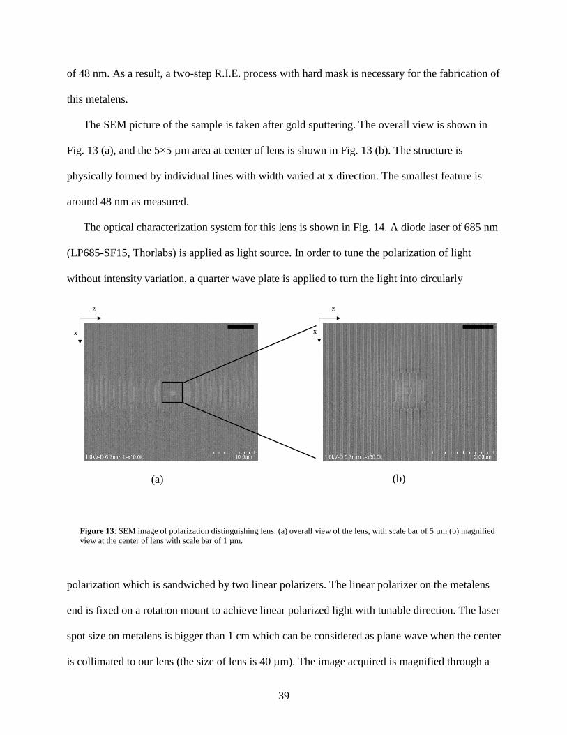
The SEM picture of the sample is taken after gold sputtering. The overall view is shown in
Fig. 13 (a), and the 5×5 µm area at center of lens is shown in Fig. 13 (b). The structure is
physically formed by individual lines with width varied at x direction. The smallest feature is
around 48 nm as measured.
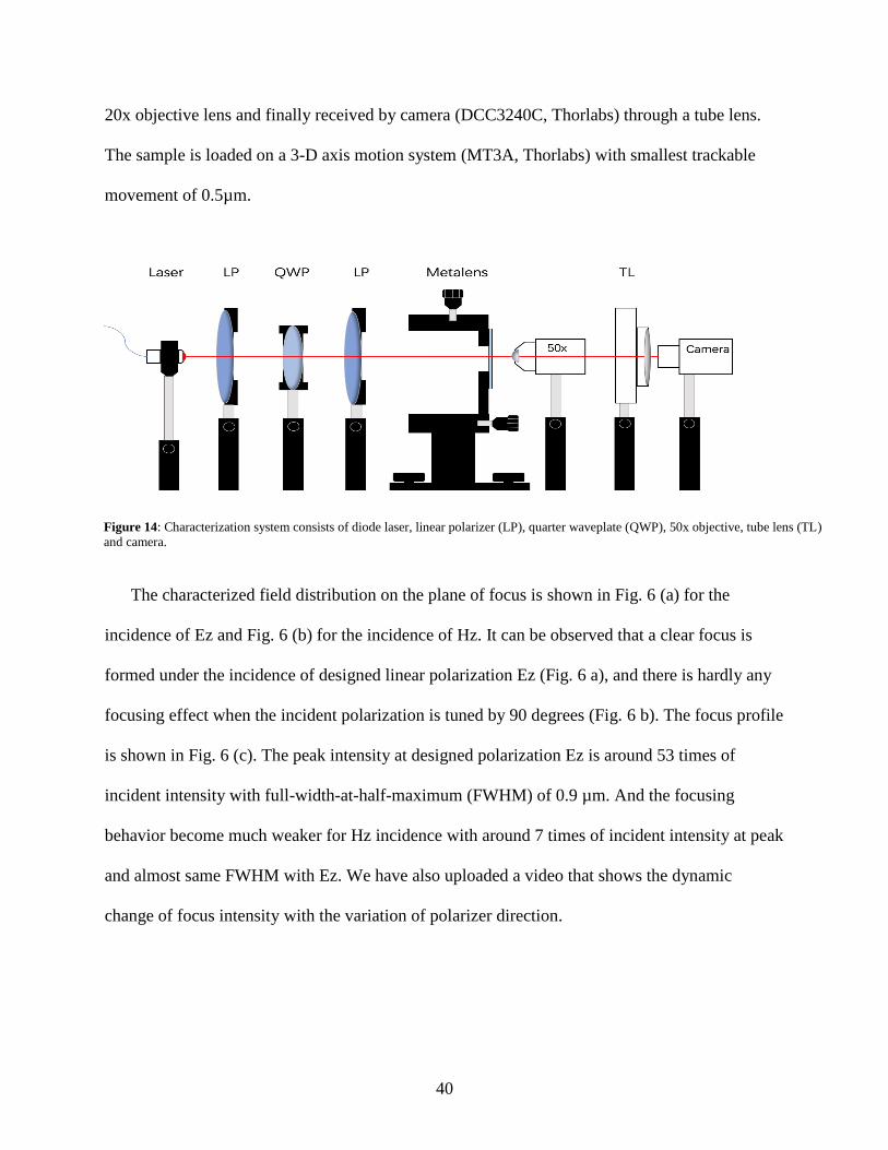
The optical characterization system for this lens is shown in Fig. 14. A diode laser of 685 nm
(LP685-SF15, Thorlabs) is applied as light source. In order to tune the polarization of light
without intensity variation, a quarter wave plate is applied to turn the light into circularly
polarization which is sandwiched by two linear polarizers. The linear polarizer on the metalens
end is fixed on a rotation mount to achieve linear polarized light with tunable direction. The laser
spot size on metalens is bigger than 1 cm which can be considered as plane wave when the center
is collimated to our lens (the size of lens is 40 µm). The image acquired is magnified through a
(a) (b)
z
x
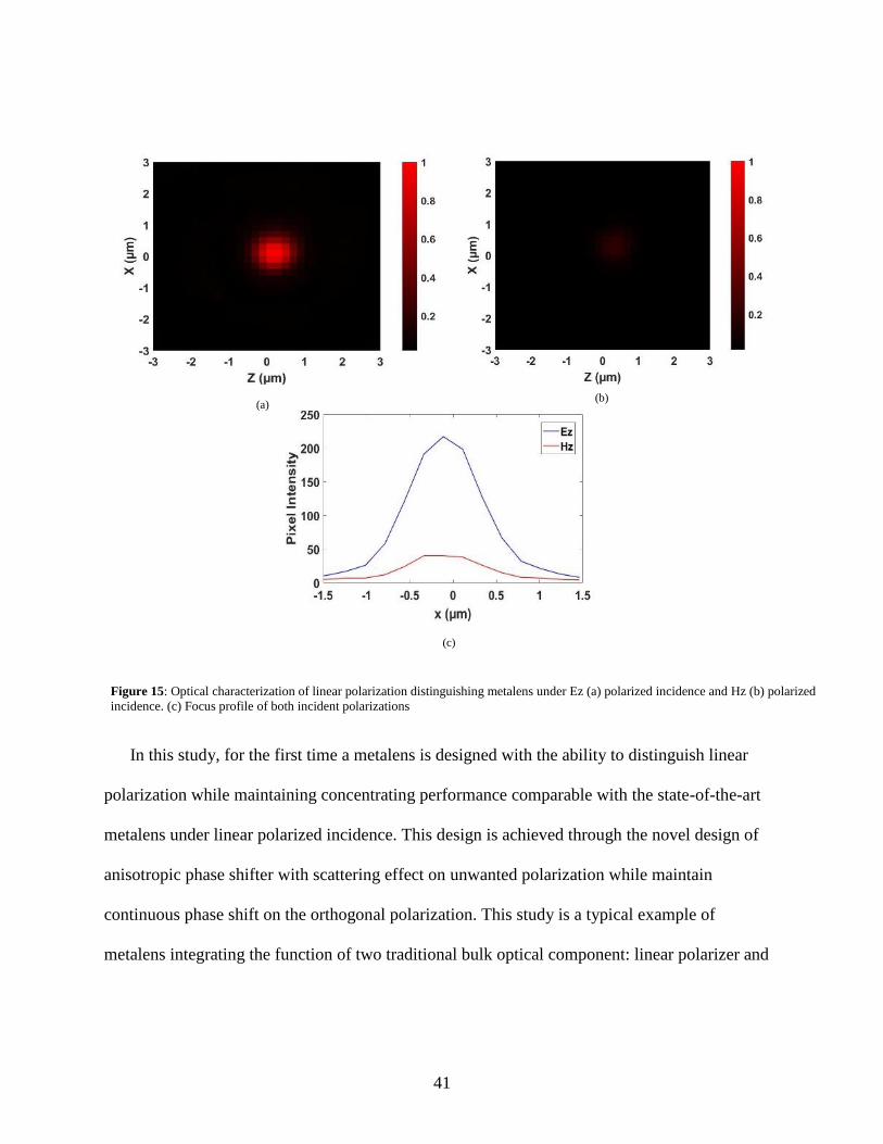
z
x
Figure 13: SEM image of polarization distinguishing lens. (a) overall view of the lens, with scale bar of 5 µm (b) magnified
view at the center of lens with scale bar of 1 µm.
40
20x objective lens and finally received by camera (DCC3240C, Thorlabs) through a tube lens.
The sample is loaded on a 3-D axis motion system (MT3A, Thorlabs) with smallest trackable
movement of 0.5µm.
The characterized field distribution on the plane of focus is shown in Fig. 6 (a) for the
incidence of Ez and Fig. 6 (b) for the incidence of Hz. It can be observed that a clear focus is
formed under the incidence of designed linear polarization Ez (Fig. 6 a), and there is hardly any
focusing effect when the incident polarization is tuned by 90 degrees (Fig. 6 b). The focus profile
is shown in Fig. 6 (c). The peak intensity at designed polarization Ez is around 53 times of
incident intensity with full-width-at-half-maximum (FWHM) of 0.9 µm. And the focusing
behavior become much weaker for Hz incidence with around 7 times of incident intensity at peak
and almost same FWHM with Ez. We have also uploaded a video that shows the dynamic
change of focus intensity with the variation of polarizer direction.
Figure 14: Characterization system consists of diode laser, linear polarizer (LP), quarter waveplate (QWP), 50x objective, tube lens (TL)
and camera.
41
In this study, for the first time a metalens is designed with the ability to distinguish linear
polarization while maintaining concentrating performance comparable with the state-of-the-art
metalens under linear polarized incidence. This design is achieved through the novel design of
anisotropic phase shifter with scattering effect on unwanted polarization while maintain
continuous phase shift on the orthogonal polarization. This study is a typical example of
metalens integrating the function of two traditional bulk optical component: linear polarizer and
(a) (b)
(c)
Figure 15: Optical characterization of linear polarization distinguishing metalens under Ez (a) polarized incidence and Hz (b) polarized
incidence. (c) Focus profile of both incident polarizations
42
concentrating lens. This study is especially attractive to applications including polarized light
microscopy and optical communication where the orthogonal signal is focused and split.
With the inherent advantage of fully controlling the wavefront, metalens/metasurfaces promises
a bright future for the integration of traditional optical components into compact and light weight
thin films (metalens is usually as thin as several hundred nanometers). The major drawback of
metalens is the difficulty and high cost of nano fabrication that holding it back from
industrialization. But with the rapid development of nano fabrication technique which is also
pushed by moore’s law, mass production of metalens can be achieved in near future.
43
Chapter 7 Continuous Achromatic Flat Subwavelength Grating Lens over whole Visible
Bandwidths
Micro lens/metasurface is one of emerging planar optical devices that have unprecedented
control of the light at nano scale and have potential applications in highly multidisciplinary fields
including imaging, sensing, spectroscopy and photovoltaics [1-6]. Recent years have seen a rapid
development of metasurface photonic devices in various aspects including design, fabrication
and characterization [1-41]. Typically, a high index contrast grating is used as individual phase
shifter to satisfy the lens focusing requirements, as it can provide relatively large phase shift
from 0 to 2π so that the light focusing condition can be met. However, the high index contrast
gratings gives rise to a significant chromatic behavior of the micro lens and achieving achromatic
focusing over certain bandwidth turns out to be very challenging [36-40]. The achromatic
focusing capability is critical for a variety of applications, as light sources (e.g., light emitting
diodes) or the signal (e.g., photoluminescence and fluorescence signals) has a substantial
bandwidth, especially in the visible wavelength range. Great efforts have been made along this
direction but until now, only narrow bandwidth in the visible wavelength has been achieved for
continuous achromatic behavior in visible wavelength [36]. In this work, for the first time we
have demonstrated the continuous achromatic micro lens covering the whole visible wavelength
based on a relatively low index contrast gratings. Because of the unique chromatic phase shift
behavior of polymer nano structure, we have demonstrated a continuous broadband
subwavelength achromatic microlens which can cover 250 nm of visible bandwidths (from 435
nm to 685 nm) with focal shift less than 5%. Our work is a critical step further to achieve the
44
promises made by the flat micro lens that is comparable with image qualities obtained by the
commercial objective [9].
The design strategy of a micro lens/metasurface is fundamentally a phase matching
mechanism [1,7]. This process relies on precise matching of one phase at the focus point by a
number of phase shifters fabricated at different locations throughout the lens, and these phase
shifters work independently to tune light wave into different phases according to its location. The
relationship of designed phase and phase shifter’s location in two-dimensional domain is
illustrated in an alteration of equation (1), shown as Eq. (1-1):
ϕ(x) − ϕ(0) =2𝜋
𝜆(√𝑥2 + 𝑓2 − 𝑓) = Δϕ (1-1)
Where 𝜆 is the incident wavelength, f is the designed focal length, x is the distance between
the phase shifter and the center of the lens, ϕ(𝑥) is the phase needed for this phase shifter, and
ϕ(0) is the phase at the center of lens. With careful selection of nano structures at different
location, a planar micro lens is designed with the same phase overlap at the focus by a number of
phase shifters. However, this process can be significantly affected when the wavelength of
incident light source is varied, which causes the chromatic behavior due to the high-index
contrast materials.
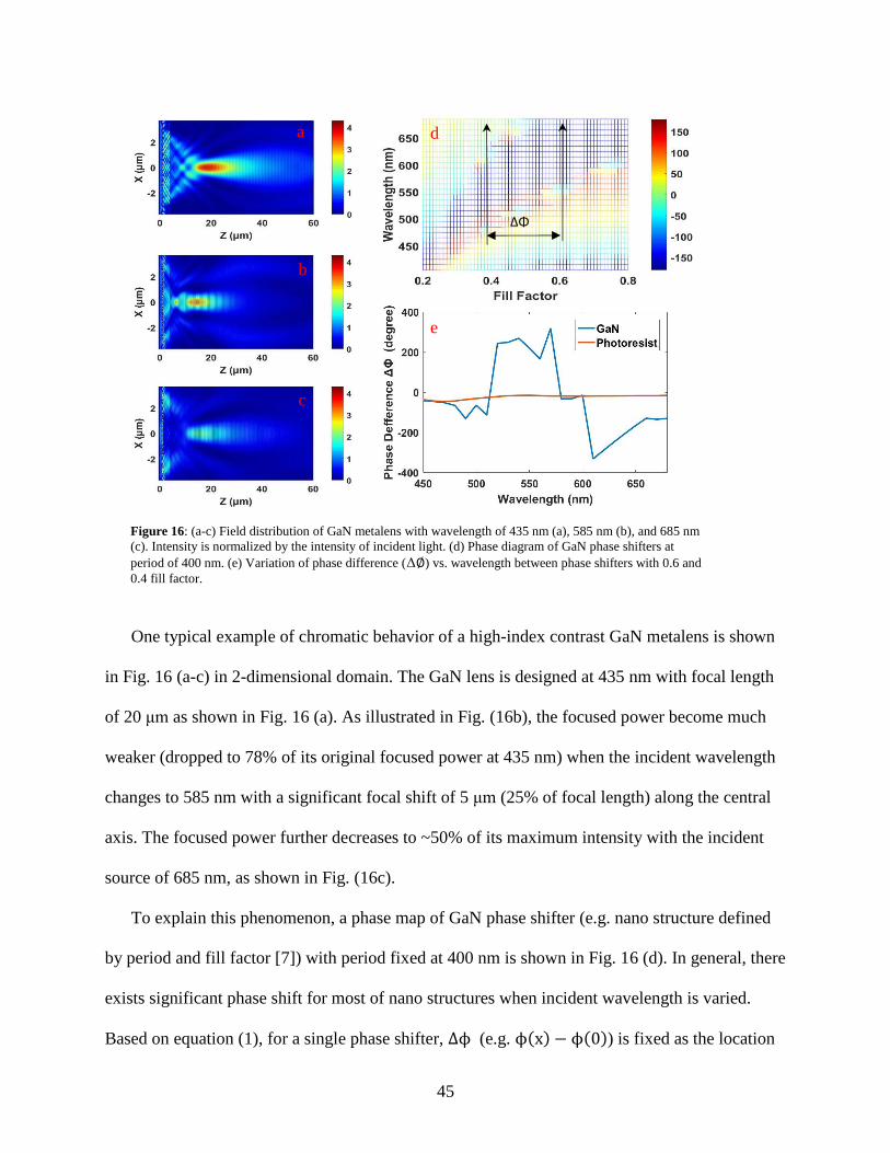
45
One typical example of chromatic behavior of a high-index contrast GaN metalens is shown
in Fig. 16 (a-c) in 2-dimensional domain. The GaN lens is designed at 435 nm with focal length
of 20 μm as shown in Fig. 16 (a). As illustrated in Fig. (16b), the focused power become much
weaker (dropped to 78% of its original focused power at 435 nm) when the incident wavelength
changes to 585 nm with a significant focal shift of 5 μm (25% of focal length) along the central
axis. The focused power further decreases to ~50% of its maximum intensity with the incident
source of 685 nm, as shown in Fig. (16c).
To explain this phenomenon, a phase map of GaN phase shifter (e.g. nano structure defined
by period and fill factor [7]) with period fixed at 400 nm is shown in Fig. 16 (d). In general, there
exists significant phase shift for most of nano structures when incident wavelength is varied.
Based on equation (1), for a single phase shifter, Δϕ (e.g. ϕ(x) − ϕ(0)) is fixed as the location
a
b
c
ΔΦ
d
e
Figure 16: (a-c) Field distribution of GaN metalens with wavelength of 435 nm (a), 585 nm (b), and 685 nm
(c). Intensity is normalized by the intensity of incident light. (d) Phase diagram of GaN phase shifters at
period of 400 nm. (e) Variation of phase difference (Δ∅) vs. wavelength between phase shifters with 0.6 and
0.4 fill factor.
46
of phase shifter is determined during the designing process. If we pick two typical phase shifter
in Fig. 16 (d), for example, assuming that fill factor =0.4 as ϕ(x) and fill factor =0.6 as ϕ(0),
their Δϕ vs. wavelength is shown as blue line in Fig. 16 (e). The dramatic variation of Δϕ over
the change of wavelength indicating that it is significantly wavelength dependent which further
leads to the significant chromatic loss for micro lens as shown in Fig. 16 (a-c). This means that
even though conventional planar micro lens can be formed by phase shifters (nano structures)
with a variety of shapes and combination methods, an inevitable and considerable chromatic loss
always exist.
Previous efforts have been made to engineer achromatic behavior of metalens/reflectors, such
as maintaining its focus property within a 60 nm bandwidth [37], or at multiple wavelengths [38-
41]. However, the design of an achromatic lens that can cover whole visible band is still very
challenging, due to the huge chromatic phase shift of conventional dielectric phase shifters with
high refractive index (e.g. GaN and TiO2).
7.1 Results
In our works, we have discovered that it is possible to design subwavelength metasurface
lens with low refractive index materials (e.g. polymer-ZEP520A, a commercial E-beam
photoresist material with refractive index 1.56). The most impressive advantage of this polymer
based micro lens is its broadband behavior. For comparison, a polymer micro lens (Polymer lens
A) is designed with similar size and focal length (as compared to above GaN micro lens), whose
field distribution is shown in Fig. 17 (a-c). Unlike GaN micro lens, the polymer micro lens gives
similar field distribution over three wavelengths across nearly all visible bandwidth (435 nm, 585
47
nm, and 685 nm) and maintains over 85% of its focus power in the mean time. For example, the
polymer lens A remains 96% of its maximum focus power at 685 nm while the GaN counterpart
remains only 55%. The reason of its superior achromatic behavior is rooted from significantly
small variation of Δϕ over a large bandwidth (Fig. 17 d). One example is shown as the orange
line in Fig. 16 (e), that the Δϕ of polymer phase shifter only changed around 26 degree which is
in a stark contrast with its GaN counterpart.
Even though polymer lens A maintains much better focus over 250 nm of visible bandwidth
(435 nm to 685 nm) compared to a GaN counterpart, there exist a significant focal shift of 26%,
and its focal length keeps varying throughout the visible bandwidth, shown as the orange line in
Fig. 17 (e). One important question arises: are we able to design an achromatic micro lens that
has minimum chromatic focal shift across the full visible wavelength?
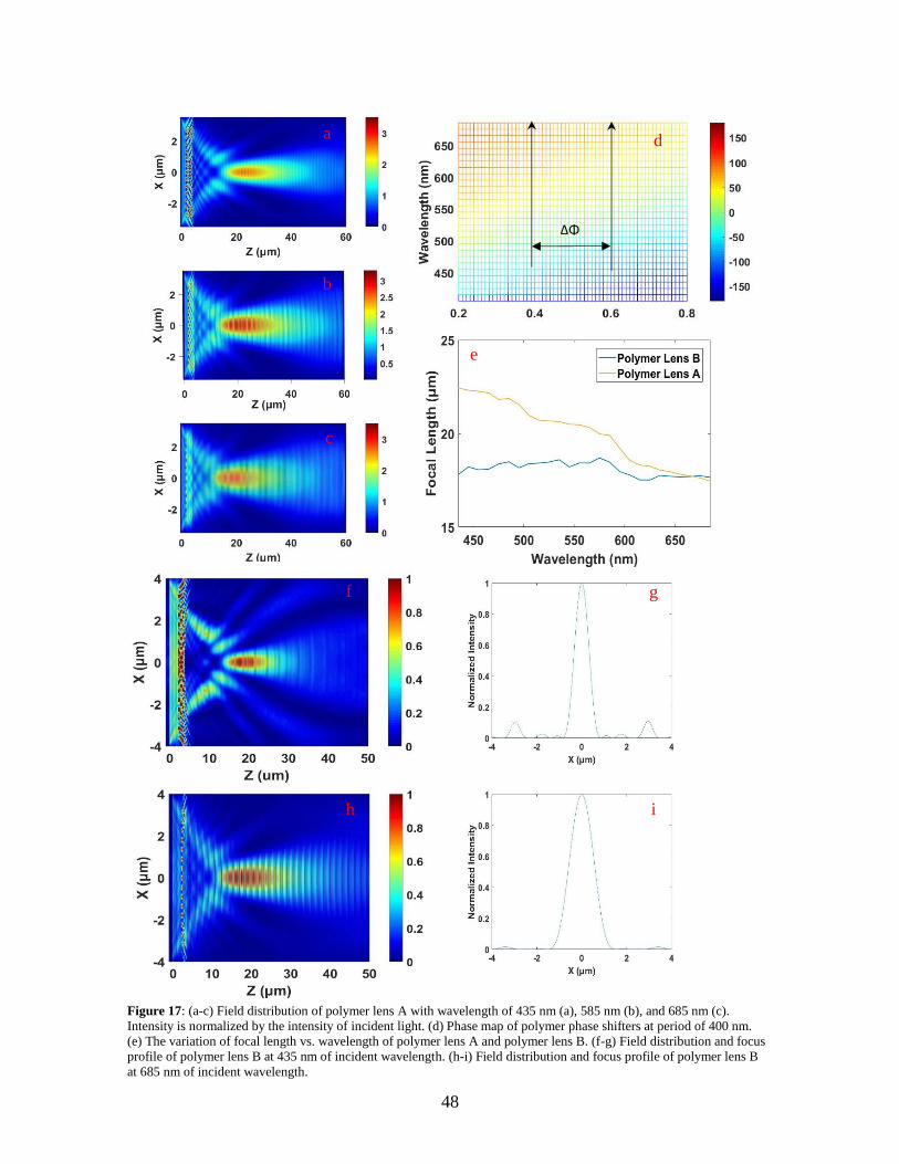
48
a
b
c
ΔΦ
f g
h i
d
e
Figure 17: (a-c) Field distribution of polymer lens A with wavelength of 435 nm (a), 585 nm (b), and 685 nm (c).
Intensity is normalized by the intensity of incident light. (d) Phase map of polymer phase shifters at period of 400 nm.
(e) The variation of focal length vs. wavelength of polymer lens A and polymer lens B. (f-g) Field distribution and focus
profile of polymer lens B at 435 nm of incident wavelength. (h-i) Field distribution and focus profile of polymer lens B
at 685 nm of incident wavelength.
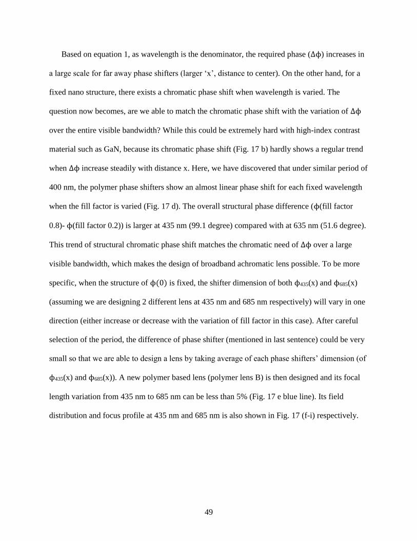
49
Based on equation 1, as wavelength is the denominator, the required phase (Δϕ) increases in
a large scale for far away phase shifters (larger ‘x’, distance to center). On the other hand, for a
fixed nano structure, there exists a chromatic phase shift when wavelength is varied. The
question now becomes, are we able to match the chromatic phase shift with the variation of Δϕ
over the entire visible bandwidth? While this could be extremely hard with high-index contrast
material such as GaN, because its chromatic phase shift (Fig. 17 b) hardly shows a regular trend
when Δϕ increase steadily with distance x. Here, we have discovered that under similar period of
400 nm, the polymer phase shifters show an almost linear phase shift for each fixed wavelength
when the fill factor is varied (Fig. 17 d). The overall structural phase difference (ϕ(fill factor
0.8)- ϕ(fill factor 0.2)) is larger at 435 nm (99.1 degree) compared with at 635 nm (51.6 degree).
This trend of structural chromatic phase shift matches the chromatic need of Δϕ over a large
visible bandwidth, which makes the design of broadband achromatic lens possible. To be more
specific, when the structure of ϕ(0) is fixed, the shifter dimension of both ϕ435(x) and ϕ685(x)
(assuming we are designing 2 different lens at 435 nm and 685 nm respectively) will vary in one
direction (either increase or decrease with the variation of fill factor in this case). After careful
selection of the period, the difference of phase shifter (mentioned in last sentence) could be very
small so that we are able to design a lens by taking average of each phase shifters’ dimension (of
ϕ435(x) and ϕ685(x)). A new polymer based lens (polymer lens B) is then designed and its focal
length variation from 435 nm to 685 nm can be less than 5% (Fig. 17 e blue line). Its field
distribution and focus profile at 435 nm and 685 nm is also shown in Fig. 17 (f-i) respectively.
50
Figure 18: (a) The SEM picture of polymer based planar micro lens (polymer lens B). (b-d) Characterized focal plane intensity
distribution of polymer based planar micro lens at 685 nm, 520 nm, and 405 nm of incident light. (e-g) 3-D focus profile at 685
nm, 520 nm, and 405 nm of incident light. (h-j) Characterization and simulation focus profile at 685 nm, 520 nm, and 405 nm of
incident light. Intensity of focus is normalized by intensity of incident wave.
Fig. 18 (a) shows the SEM picture of polymer based metalens (Polymer lens B) fabricated
through E-beam lithography process. This design is achieved by spining the 2D structure on x-y
plane around its central axis, which ends up with a bull’s eye structure with diameter of around 7
μm. This micro lens’s focus property is then measured through a laser-based system. Since diode
lasers are linearly polarized, light processing and focusing happens in a 2-D domain which is the
a
b c d
e f g
h i j
51
same as previous simulation. Three single wavelength diode lasers are utilized as source (685
nm, 520 nm and 405 nm respectively), and their intensity distribution profile at focus plane are
demonstrated as Fig. 18 (b-d) in 2-D and Fig. 18 (e-g) in 3-D. It can be observed that the lens can
achieve a clear focus for three wavelengths across 280 nm range. While more side peaks can be
observed at 405 nm of incident light (Fig. 18d & g) compared with 685 nm (Fig. 18 b & e). This
came from increased phase mismatch when away from our original design at 435 nm, which also
lowered the focused intensity. The focus profiles are also plotted and shown on Fig. 18 (e-g) for
simulation and Fig. 18 (h-j) for characterization at 405 nm, 520 nm, and 685 nm respectively. As
can be observed, the measured maximum intensity at the focus is in good agreement with the
simulation results. One interesting point is that the measured full width at half maximum is
around 0.6 micron larger than simulation result for all three wavelengths, which may indicate
further fabrication process improvement. The measured focal lengths are 17.5 ± 1 microns for all
three wavelengths which shows a good consistency with simulation.
7.2 Discussion
The low-index contrast all dielectric materials are not limited to the polymer we used in this
work, other representative low-index contrast materials like SiO2 and Si3N4, etc. can also be
utilized to achieve continuous broadband achromatic behavior covering the whole visible
wavelength, in which CMOS compatible fabrication and large-scale manufacturing process can
be fully utilized. There are several potential advantages for a polymer micro lens. Usually,
subwavelength nano structure utilizing traditional high-index contrast materials (Si3N4, TiO2,
GaN) requires plasma aided thin film deposition and/or reactive ion etching. While the polymer
52
used here (ZEP520A) is a typical E-beam photoresist, the complete fabrication process of
metalens is significantly simplified, only E-beam patterning process is needed. In this way, many
challenging nano fabrication imperfections can be avoided, such as R.I.E lag related taper
structure [42], or surface defects associated with lift-off process. Furthermore, because of the
flexible nature of polymer materials, future integrated wearable devices may be promising out of
our works.
The discovery of relatively low-index contrast based subwavelength nano structure has led to
the first continuous achromatic metalens working at the whole visible wavelength. Its broadband
behavior in the whole visible wavelengths is demonstrated by both simulation and experiments.
This is the first time that a metalens using low-index contrast soft material at micron scale
(smaller than 10 microns) is fabricated and characterized. Our work is a important step further to
achieve the ultimate goals expected from the flat micro lens that is potentially compact and
CMOS compatible on chip, and is comparable to image qualities obtained by the commercial
objective.
7.3 Methods
Numerical Simulation: Two-dimensional finite difference time domain (FDTD) method is
performed using Omnisim FDTD software for all simulation in this study. Perfect match layer
(PML) is applied on all boundaries of simulation window for the simulation of micro lens. For
the preparation of phase map, periodical boundary condition is applied on the boundary of X
direction and PML is applied on the boundary of Z direction. Refractive index of SiO2 substrate

53
and air are 1.45 and 1 respectively. Imaginary part of refractive index for all materials are set
zero, sufficient small grid size and sufficient long simulation times are applied for the simulation.
Light source is set as TE polarized single wavelength continues wave.
Nano Fabrication: Polymer material ZEP520A is acquired from ZEON Corporation which is a
commercial electron beam resist. Firstly, 400 nm of ZEP520A is spin coated on silica wafer,
which is then baked on hot plate at 180 0C for 3 min. The sample is then spin coated with a layer
of conductive material to prepare for E-beam lithography. JOEL JBX-6300 FS electron beam
lithography system is utilized to write the lens structure under 20 kV. After the exposure with
electron beam, the sample is developed in ZED-N50 then rinsed thoroughly with lens left on the
wafer. The lens is fabricated in 5x5 array, and a micro scale pointer is also fabricated for the
convenience of finding the structure.
Optical Measurements: Three diode lasers with wavelength of 685 nm, 520 nm and 405 nm
are utilized as source (LP685, LP520 and LP405-SF, Thorlabs Inc.). The sample is mounted on 3
directional motion system MT3A (Thorlabs Inc.) which is directly illuminated by the laser. The
image is then magnified by an objective (Olympus LMPlanFLN 50x) and tube lens (Thorlabs
TTL 200) system before captured by camera (Thorlabs DCC1545M). A schematic graph of
characterization set up is provided in supplementary material (S3). The laser shed on the sample
lens has spot size ~3 mm which is much larger than the size of lens. So when we focus on a
10x10 micrometers area, the incident source is considered as plane wave rather than a Gaussian
beam. Before the fabrication of micro lens, several Au alignment marks (50x50 micron) are
fabricated on the silica wafer with thickness around 20 nm. Those alignment marks will not only
help us to find our structure in optical systems but also act as an important reference of size. We
first find the location of the micro lens and its nearest alignment mark. Then with fine adjustment
54
of the sample stage (Thorlabs MT3A) in Z direction, the objective is focused on the alignment
mark. By recording the Z coordinate and plus 380 nm (the thickness of alignment mark is 20 nm
and the thickness of lens is 400nm), the Z coordinate of the lens surface is acquired. Next step is
to tune the x-y coordinate to move to the lens area. Then the lens is moved carefully away from
the objective while the real-time intensity profile of the central axis (x and y axis at center point)
are monitored. The focus is found where both x and y axis presenting maximum intensity. The
focal length is acquired by calculating the distance moved from the lens surface to the focus in Z
direction. The measurement error of focal length mainly generates from two aspects: 1. The
resolution of translation system (Thorlabs MT3A) is 0.5 micro meter. 2. When determine the Z
coordinate of the lens surface, the Au alignment mark has thickness of 0.02 micro meter, thus
create an error of 0.02 micro meter (in worst case).
55
Chapter 8 Transmission Enhancement of Subwavelength Grating Micro Lens by Tapered
Nano Structure
Subwavelength micro lens is one of the emerging planar micro optical devices with great
potential in a variety of applications [1-8]. Among this field, high refractive index contrast nano
structures shows great advantages in areas such as spectrally modification of optical wave front
[2]. These advantages have enabled the micro lens to be designed in a scale ranging from
microns to several millimeters with focus size less than a micron.
Based on the subwavelength nature of phase shifters, physical realization of the micro lens
relies on nano fabrication techniques. To be specific, it can be either fabricated through reactive
ion etching (top down process) or deposition then lift-off (bottom up process). Despite the
difference in processes details, both of the two techniques have one common challenge that it is
extremely difficult to fabricate structures with high aspect ratio (e.g. ratio higher than 5:1
thickness vs. width). For planar gratings lens that is designed under linearly polarized incidence
(e.g. utilization of propagation phase [2, 4] not Pancharatnam-Berry phase), different phase shift
is created by altering the effective refractive index. In order to achieve enough phase shift in
visible wavelength with limited thickness (e.g. low aspect ratio), researchers have looked into
high refractive index material such as GaN [3] and TiO2 [9]. While high refractive index
materials are enabling phase shifters more phase shift with comparatively low aspect ratio, their
transmission may experience a significant drop.
In order to design an optimum planar micro lens, one should either increase the phase
coverage of low index material nano structures or increase the transmission of high index
56
material nano structures. While the most effective way of increasing phase coverage of nano
structures is to increase its thickness (increase single mode propagation length inside the
structure). While this idea may not be practical, as we already approaching the limit of current
nano fabrication with 80 nm of feature size and 400 nm of thickness. Upon realizing this, we
have to consider through another direction as mentioned previously, that is to increase the
transmission of high index material nano structures.
In this work, we have discussed possible transmission enhancement mechanisms and their
feasibilities with the application of planar micro lens. In addition, we have proposed the
subwavelength tapered nano structure to enhance the transmission of TiO2 nano structure as
phase shifters of micro lens under linearly polarized light. The enhancement effect is then
examined by numerical simulation (FDTD) through subwavelength micro grating lens in 2-
dimensional domain.
8.1 Design and Simulation Results
The design of subwavelength micro grating lens follows a widely acknowledged phase matching
process [3-6]. Basically, the micro grating lens is consisting of a group of phase shifters (e.g.
subwavelength nano gratings defined by period and fill factor [2, 5]) that each of them will tune
the phase of light (that pass through this phase shifter) based on its dimension and refractive
index. To be specific, the phase profile of a typical focusing subwavelength grating lens is
governed by the equation:
ϕ(x) − ϕ(0) =2𝜋
𝜆(√𝑥2 + 𝑓2 − 𝑓) = −Δϕ (1)
57
Where 𝜆 is the incident wavelength, f is the designed focal length, x is the distance between the
phase shifter and the center of the lens, ϕ(𝑥) is the phase needed for this phase shifter, and ϕ(0)
is the phase at the center of lens. Δϕ is the phase difference created by the nano structure at this
location. For micro grating lens, necessary phase shifts (e.g. ϕ(𝑥)) can be acquired through
different subwavelength nano structures (gratings) defined by period and fill factor (also known
as duty cycle [4, 5]). In other words, the focusing subwavelength grating lens is designed by
selecting appropriate grating structures to fulfill the phase profile of a focusing lens (e.g. eq. 1).
To compare the phase shift and transmission of high index and low index nano structures, we
have chosen two materials as Si3N4 (refractive index 2.0) and TiO2 (refractive index 2.55) and
conducted the study through two dimensional finite different time domain method (FDTD) under
light incidence of 685 nm, showed in Fig. 1. Nano structures in Fig. 1 are defined by period and
fill factor (also known as duty cycle), and the dimensions presented here covers most
conventional phase shifter dimensions in 2D domain. Perfect match layer (PML) is applied on
boundaries (both ends) of incident direction to truncate simulation area. Periodical boundary
condition is applied (on other 2 boundaries) for the extension of grating during the creation of
phase map. Sufficiently long time steps and sufficiently small grid size are utilized to ensure the
precision of FDTD simulation. The refractive index of air is set as 1 and the phase shifter is
mounted on a glass substrate with refractive index of 1.5. The imaginary part of refractive index
is neglected.

58
Showed in Fig. 19 (a) for a single Si3N4 phase shifter with thickness of 400 nm, the phase can
be shifted in a range of 68 degrees (0.37π) with the variation of nano structure dimensions
(period from 0.3 to 0.45 μm, fill factor from 0.2 to 0.8). In comparison, TiO2 counterparts (in
same dimensions) can cover all phase shift (e.g. 360 degree), as showed in Fig. 19 (b). While the
transmission rate for this group of TiO2 phase shifters can be as low as 20% (Fig. 19 d), in sharp
comparison with their Si3N4 counterparts with transmission above 80% for most of phase shifters
shown in Fig. 19 (c).
Figure 19: Phase diagrams and transmission for single phase shifters with thickness of 400 nm. (a) Phase diagram for Si3N4
phase shifter. (b) Phase diagram for TiO2 phase shifter. (c) Transmission for Si3N4 phase shifter. (d) Transmission for TiO2
phase shifter. The thickness of all phase shifters is fixed at 400 nm and the incident wavelength is fixed at 685 nm.
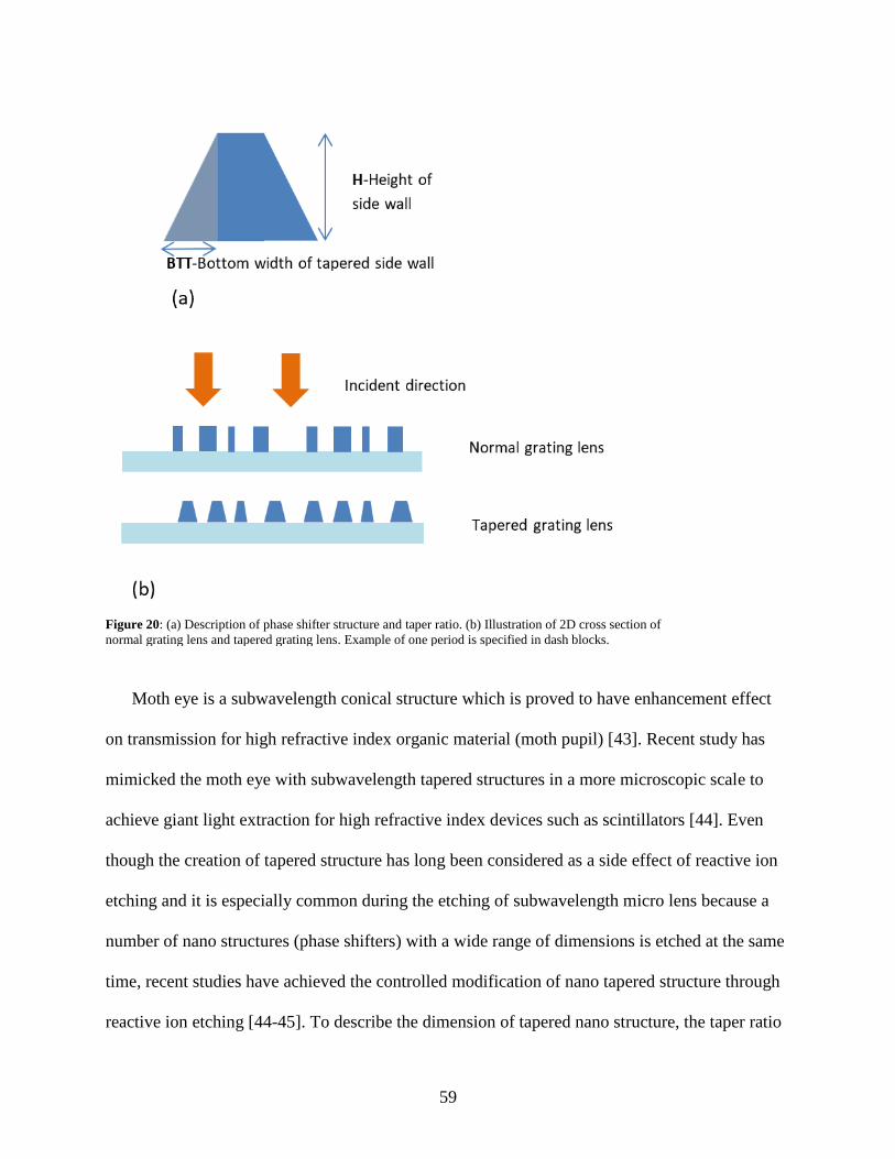
59
Moth eye is a subwavelength conical structure which is proved to have enhancement effect
on transmission for high refractive index organic material (moth pupil) [43]. Recent study has
mimicked the moth eye with subwavelength tapered structures in a more microscopic scale to
achieve giant light extraction for high refractive index devices such as scintillators [44]. Even
though the creation of tapered structure has long been considered as a side effect of reactive ion
etching and it is especially common during the etching of subwavelength micro lens because a
number of nano structures (phase shifters) with a wide range of dimensions is etched at the same
time, recent studies have achieved the controlled modification of nano tapered structure through
reactive ion etching [44-45]. To describe the dimension of tapered nano structure, the taper ratio
Figure 20: (a) Description of phase shifter structure and taper ratio. (b) Illustration of 2D cross section of
normal grating lens and tapered grating lens. Example of one period is specified in dash blocks.
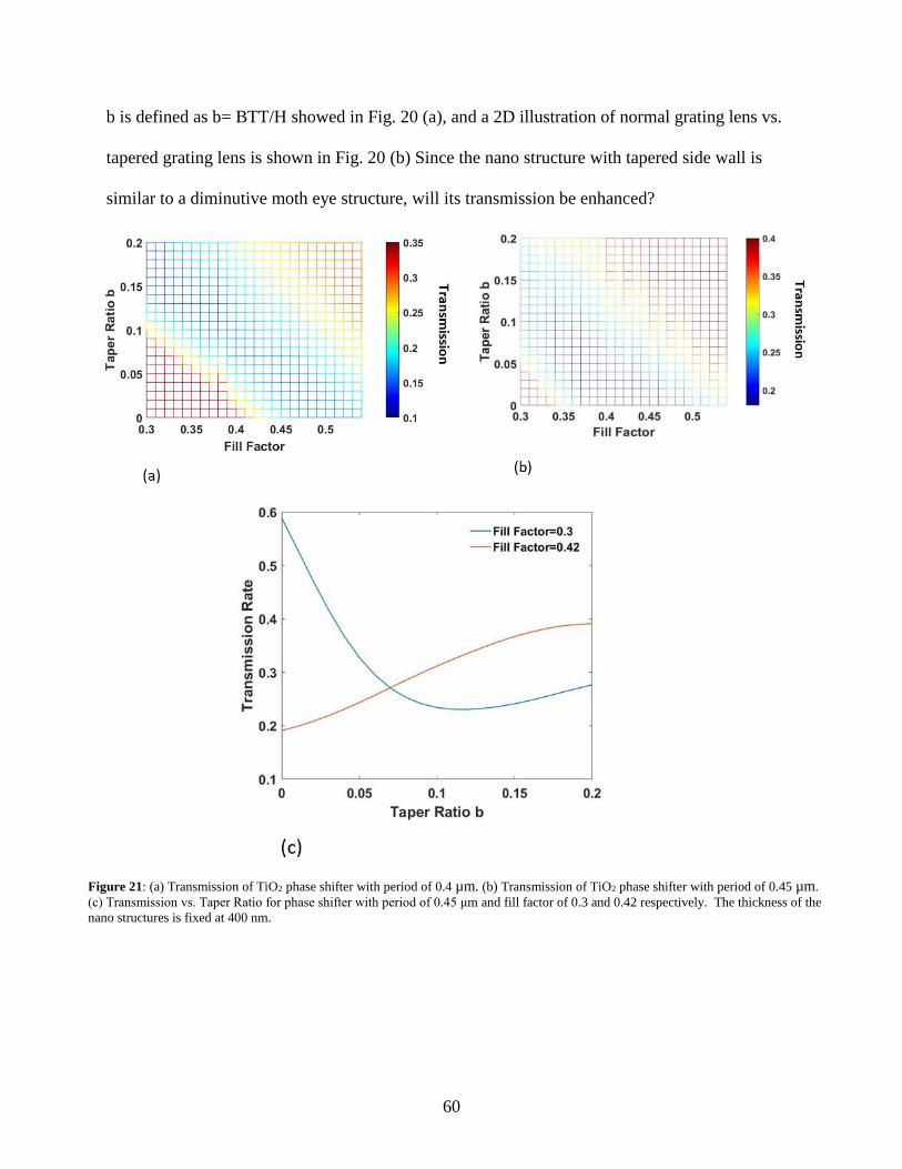
60
b is defined as b= BTT/H showed in Fig. 20 (a), and a 2D illustration of normal grating lens vs.
tapered grating lens is shown in Fig. 20 (b) Since the nano structure with tapered side wall is
similar to a diminutive moth eye structure, will its transmission be enhanced?
Figure 21: (a) Transmission of TiO2 phase shifter with period of 0.4 µm. (b) Transmission of TiO2 phase shifter with period of 0.45 µm.
(c) Transmission vs. Taper Ratio for phase shifter with period of 0.45 μm and fill factor of 0.3 and 0.42 respectively. The thickness of the
nano structures is fixed at 400 nm.
61
To answer this question, we pick the period of 400 nm and 450 nm (frequently used when
designing micro lens) and studied its transmission when varying fill factor and taper ratio shown
in Fig. 21.
As can be observed in Fig. 21 (a & b), the transmission of nano structure varies when its fill
factor and taper ratio is altered. With the period of 0.4 µm, for fill factor below 0.4, the
transmission decreases with the increase of taper ratio. For period of 0.45 µm, same trend can be
found when fill factor is below 0.35 (Fig. 21 b). One example is drawn in Fig. 21 c as blue line.
This is because for nano structures with low fill factor, the major area is covered by air and their
high transmission is mainly resulted from low material density. The creation of taper structure on
low fill factor nano structures adds a major portion of material to the original structure. As a
result, the blocking effect caused by the addition of taper side wall plays a more significant role
compared with the effect of transmission enhancement. On the other hand, for nano structures
with fill factor larger than 0.45 (Fig. 21 a), the transmission increases with the increase of taper
ratio. And the same trend is found for fill factor larger than 0.4 with period of 0.45 micron (Fig.
21 b). This indicates that, the taper enhancement effect become dominate beyond this point (fill
factor of 0.45) at the period of 0.4 µm. At this point, we can conclude that, the tapered structure
has transmission enhancement effect when the fill factor exceeds certain threshold. This is
because the taper-blocking and taper-enhancement effect together affecting the transmission of
tapered subwavelength nano structure.
While we can achieve high transmission with high refractive index material (e. g. TiO2) in
low fill factor area, we discovered that it is not possible to design a micro lens with only low fill
factor nano structures. As mentioned at the beginning, the design of planar micro lens relies on a
known phase matching process, thus enough phase coverage is necessary in order to form a
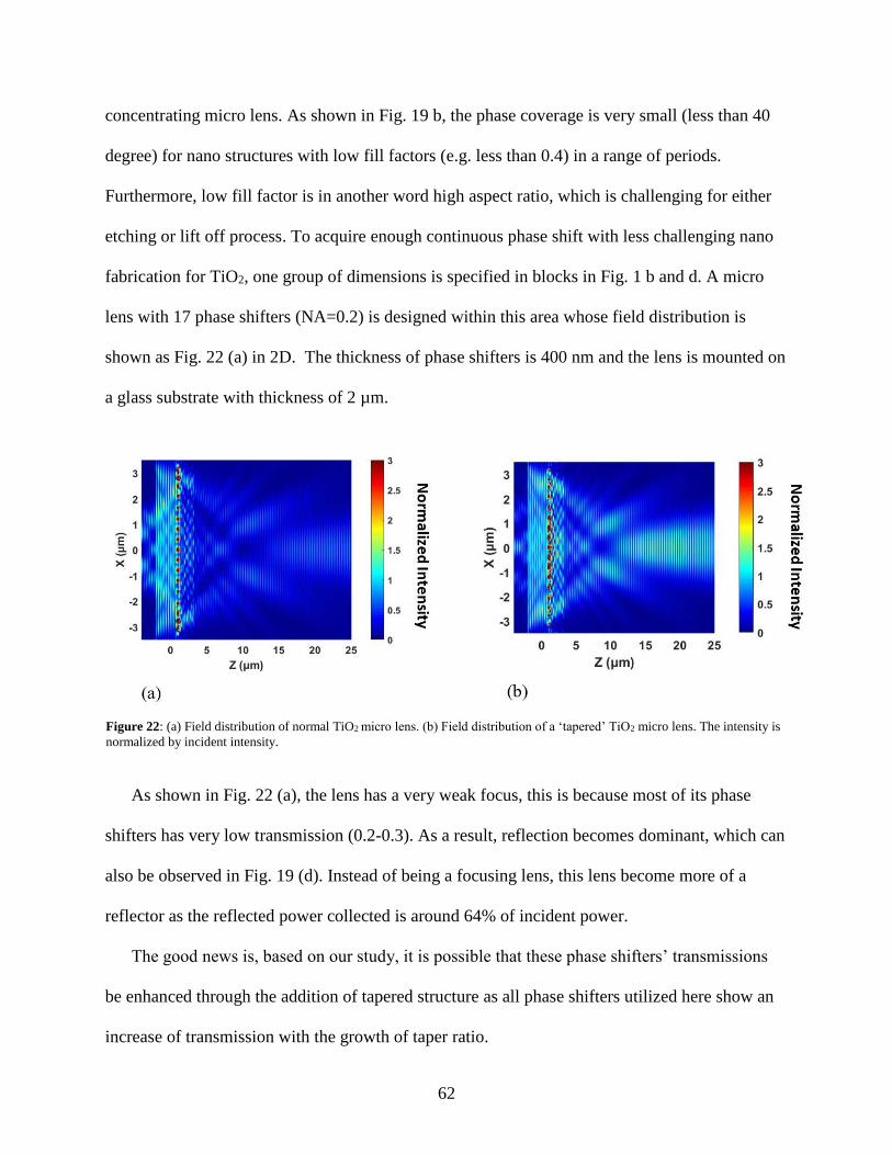
62
concentrating micro lens. As shown in Fig. 19 b, the phase coverage is very small (less than 40
degree) for nano structures with low fill factors (e.g. less than 0.4) in a range of periods.
Furthermore, low fill factor is in another word high aspect ratio, which is challenging for either
etching or lift off process. To acquire enough continuous phase shift with less challenging nano
fabrication for TiO2, one group of dimensions is specified in blocks in Fig. 1 b and d. A micro
lens with 17 phase shifters (NA=0.2) is designed within this area whose field distribution is
shown as Fig. 22 (a) in 2D. The thickness of phase shifters is 400 nm and the lens is mounted on
a glass substrate with thickness of 2 µm.
As shown in Fig. 22 (a), the lens has a very weak focus, this is because most of its phase
shifters has very low transmission (0.2-0.3). As a result, reflection becomes dominant, which can
also be observed in Fig. 19 (d). Instead of being a focusing lens, this lens become more of a
reflector as the reflected power collected is around 64% of incident power.
The good news is, based on our study, it is possible that these phase shifters’ transmissions
be enhanced through the addition of tapered structure as all phase shifters utilized here show an
increase of transmission with the growth of taper ratio.
Figure 22: (a) Field distribution of normal TiO2 micro lens. (b) Field distribution of a ‘tapered’ TiO2 micro lens. The intensity is
normalized by incident intensity.
63
To test the transmission enhancement of tapered structure on micro lens, a taper side wall
(specified as grey in Fig. 2 a) with b=0.15 is added to every phase shifter of the micro lens
presented in Fig. 22 (a). The field distribution of taper enhanced micro lens is shown in Fig. 22
(b). As can be observed for tapered micro lens, a focus is formed at approximately the same
place with none tapered lens (Fig. 22 a), while the intensity is increased by ~2.5 times. The
reflected power is reduced from ~64% to ~38%, and the focus efficiency with 2 μm width
(sensor is placed at the focus point with width of 2 μm) is increased from 9% to 28%. This shows
that the lens’s transmission is significantly enhanced by the tapered structure which brings huge
improvement of its focus property. Another point is one has to be aware that the addition of
tapered structure may bring extra phase shift to a nano structure which sometimes cause
significant destructive effect to the focus performance if not designed in the taper resistant area
[4]. For the design in Fig. 22 (b), most of the tapered structure are ‘taper resistant’ which means
the extra phase introduced by taper side wall is very small that may not cause a major phase
mismatch.
This transmission enhancement effect is crucial for the optimization of subwavelength
grating lens in two aspects.1. For linearly polarized incidence, considering high refractive index
material with certain fill factor is necessary for the sake of large phase coverage, the addition of
tapered side wall provides a spike on the phase shifter’s transmission. 2. It is showed that phase
shifter’s with extensively low fill factor (e.g. less than 0.3) has a high sensitivity to fabrication
defects (e.g. tapering), which results a drop of transmission, thus it is necessary to avoid nano
structures of low fill factor as long as the designed phase shifts are covered. In addition,
acknowledging the taper transmission enhancement effect, the fabrication process of micro lens
can be more flexible as the acceptable taper ratio is increased.
64
8.2 Conclusion
In summary, it is numerically demonstrated that a nano scale tapered structure can enhance the
light transmission for phase shifters made from high refractive material. A subwavelength-
grating lens is designed to examine the transmission enhancement effect. As observed, the focus
performance can be significantly increased by tapered structure. This is due to the increased
transmission for each independent phase shifters. This result is not only important for the
optimization of planar micro grating lens but also important for the design of micro-nano
diffractive optical devices utilizing materials with high refractive index.
65
Chapter 9 Taper Resistant Subwavelength Grating Micro Lens
Subwavelength lenses/metasurfaces are emerging nano devices with great potential in the area of
imaging, optical communication, and solar cells. Various lenses with different materials or nano
structures have been investigated, aimed at a number of applications, including ultra-high
resolution recognition [1], planar high numerical aperture focusing reflectors [2], laser beam
shaping [3], and concentrators [2, 4,5].
Reported subwavelength concentrating lenses are designed based mostly on a typical phase-
matching process [2,6]. To be specific, the lenses are divided into a number of individual periods
such that light passing through each period will be tuned to the same phase on the designed focus
position. Hence, the nano structure within each period is also called the “phase shifter.” The
required phase of a phase shifter in a two-dimensional domain is calculated as equation (1),
where x stands for the distance between the shifter and the center of lens, and ƒ stands for the
designed focal length [2,4,6].
∅(𝑥) =2𝜋
𝜆(√𝑥2 + 𝑓2 − 𝑓) (1)
The feature sizes of these subwavelength lenses usually range from several hundred nanometers
to tens of nanometers, which are based on the required dimensions of typical phase shifters. The
basic mechanism of a shifter is to “neutralize” the phase shift generated by the subwavelength
structure and the shifter’s phase difference being caused by its location. Usually, these phase
shifters are designed to be at certain “height” (i.e., grating thickness) due to the requirements of
phase accumulation [1, 2, 4], half-wave plate limitation [1], and base resonance excitation [7].
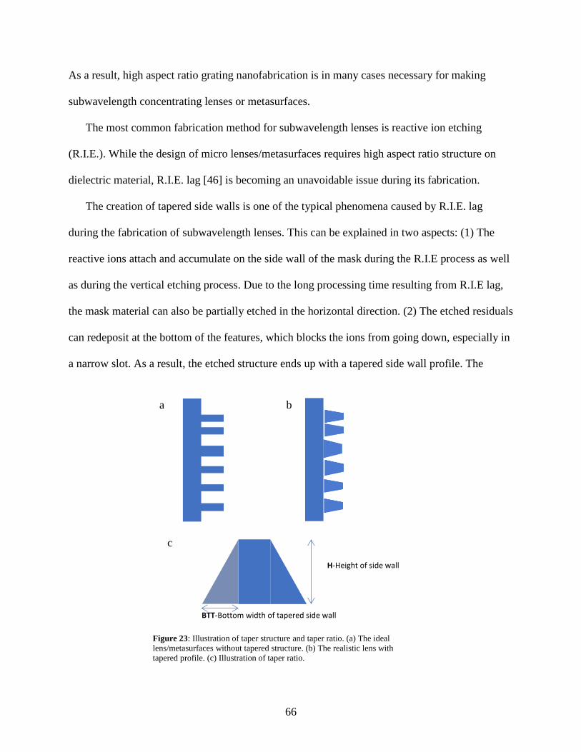
66
As a result, high aspect ratio grating nanofabrication is in many cases necessary for making
subwavelength concentrating lenses or metasurfaces.
The most common fabrication method for subwavelength lenses is reactive ion etching
(R.I.E.). While the design of micro lenses/metasurfaces requires high aspect ratio structure on
dielectric material, R.I.E. lag [46] is becoming an unavoidable issue during its fabrication.
The creation of tapered side walls is one of the typical phenomena caused by R.I.E. lag
during the fabrication of subwavelength lenses. This can be explained in two aspects: (1) The
reactive ions attach and accumulate on the side wall of the mask during the R.I.E process as well
as during the vertical etching process. Due to the long processing time resulting from R.I.E lag,
the mask material can also be partially etched in the horizontal direction. (2) The etched residuals
can redeposit at the bottom of the features, which blocks the ions from going down, especially in
a narrow slot. As a result, the etched structure ends up with a tapered side wall profile. The
a b
c
BTT-Bottom width of tapered side wall
H-Height of side wall
Figure 23: Illustration of taper structure and taper ratio. (a) The ideal
lens/metasurfaces without tapered structure. (b) The realistic lens with
tapered profile. (c) Illustration of taper ratio.
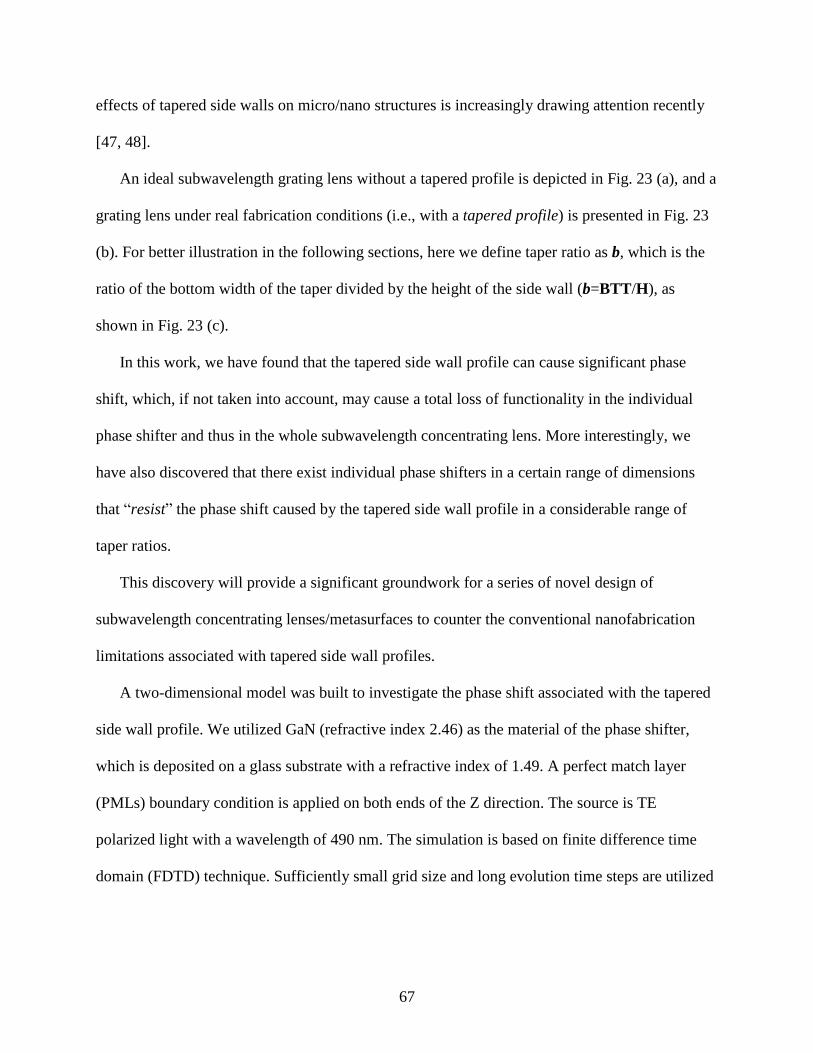
67
effects of tapered side walls on micro/nano structures is increasingly drawing attention recently
[47, 48].
An ideal subwavelength grating lens without a tapered profile is depicted in Fig. 23 (a), and a
grating lens under real fabrication conditions (i.e., with a tapered profile) is presented in Fig. 23
(b). For better illustration in the following sections, here we define taper ratio as b, which is the
ratio of the bottom width of the taper divided by the height of the side wall (b=BTT/H), as
shown in Fig. 23 (c).
In this work, we have found that the tapered side wall profile can cause significant phase
shift, which, if not taken into account, may cause a total loss of functionality in the individual
phase shifter and thus in the whole subwavelength concentrating lens. More interestingly, we
have also discovered that there exist individual phase shifters in a certain range of dimensions
that “resist” the phase shift caused by the tapered side wall profile in a considerable range of
taper ratios.
This discovery will provide a significant groundwork for a series of novel design of
subwavelength concentrating lenses/metasurfaces to counter the conventional nanofabrication
limitations associated with tapered side wall profiles.
A two-dimensional model was built to investigate the phase shift associated with the tapered
side wall profile. We utilized GaN (refractive index 2.46) as the material of the phase shifter,
which is deposited on a glass substrate with a refractive index of 1.49. A perfect match layer
(PMLs) boundary condition is applied on both ends of the Z direction. The source is TE
polarized light with a wavelength of 490 nm. The simulation is based on finite difference time
domain (FDTD) technique. Sufficiently small grid size and long evolution time steps are utilized
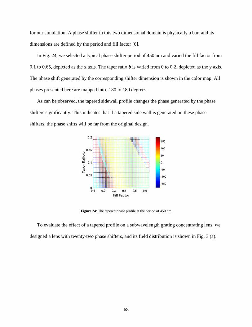
68
for our simulation. A phase shifter in this two dimensional domain is physically a bar, and its
dimensions are defined by the period and fill factor [6].
In Fig. 24, we selected a typical phase shifter period of 450 nm and varied the fill factor from
0.1 to 0.65, depicted as the x axis. The taper ratio b is varied from 0 to 0.2, depicted as the y axis.
The phase shift generated by the corresponding shifter dimension is shown in the color map. All
phases presented here are mapped into -180 to 180 degrees.
As can be observed, the tapered sidewall profile changes the phase generated by the phase
shifters significantly. This indicates that if a tapered side wall is generated on these phase
shifters, the phase shifts will be far from the original design.
Figure 24: The tapered phase profile at the period of 450 nm
To evaluate the effect of a tapered profile on a subwavelength grating concentrating lens, we
designed a lens with twenty-two phase shifters, and its field distribution is shown in Fig. 3 (a).
69
The lens in Fig. 25 has a diameter of around 12 µm with a focal length of 9.8 µm. The
focusing intensity is normalized by the incident intensity shown by the scale bar. The ideal lens
shown in Fig. 25 (a) with no taper profile has a focus intensity of 8.9. Fig. 25 (b) shows the field
distribution of the same design (i.e., same shifter dimensions) as in Fig. 25 (a), but with the
addition of a tapered sidewall profile with taper ratio b=0.15. As can be observed, the lens with a
tapered sidewall profile has completely lost its focus. To further evaluate the disappearance of
b
a
Figure 25: (a) Field distribution of grating concentrating lens with no taper
side wall. (b) Field distribution of grating concentrating lens with taper ratio
b=0.15.
70
focus power associated with tapered sidewall profile, several more simulations are performed by
varying the taper ratio between 0.05 and 0.2. As discovered, generally the focus power decreases
with the increase of taper ratio. And this reduction is critical, as a tapered side wall with only a
0.05 taper ratio can cause a 23.1% loss of focus intensity. Also, the lens completely loses its
focus when the taper ratio reaches 0.15, as the normalized focus intensity becomes smaller than
the incident light. Further increasing the taper ratio beyond 0.15 hardly affects the lens’s focus
property. The loss of focus power is mainly due to the extra phase shift generated by the tapered
sidewall profiles. As a result, light passing an individual phase shifter with a tapered profile will
not achieve the designed phase at the focus point.
To further investigate the effect of tapered side walls on individual phase shifters, we
calculated the extra phase shift of a number of phase shifters by selecting three commonly used
periods in lens design, 300 nm, 350 nm, and 450 nm, and varying the fill factor and taper ratio as
shown in Fig. 4. Here, the extra phase shift from the tapered side wall is calculated by φ(e)=φ
(t)-φ(n), where φ(e) is the extra phase, φ(t) is the phase shift generated from the tapered
phase shifter, and φ(n) is the phase shift generated from an ideal phase shifter without tapered
side walls.
Interestingly, we discovered in Fig. 4 that there are areas in the phase diagram where the
extra phase remains nearly zero (e.g. φ(e)=0) when the taper ratio is varied through a
considerable range. These areas are specified in blocks in Fig. 4. For example, in Fig. 4 (a), a
phase shifter with a period of 300 nm and a fill factor ranging from 0.56 to 0.6 generates
negligible phase shift with the addition of a tapered side wall with taper ratio below 0.2. For
convenience, this area (confined by dashed blocks) in the phase color map is called the “taper
resistant area.” It can be observed in Fig. 4 (b) that the taper resistant area for period 350 nm is
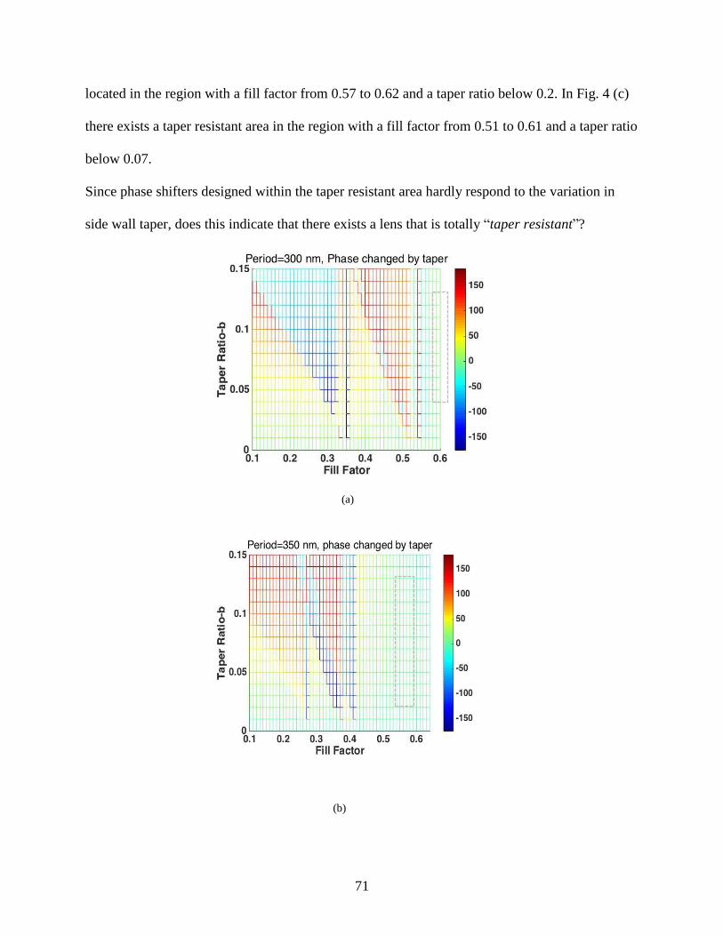
71
located in the region with a fill factor from 0.57 to 0.62 and a taper ratio below 0.2. In Fig. 4 (c)
there exists a taper resistant area in the region with a fill factor from 0.51 to 0.61 and a taper ratio
below 0.07.
Since phase shifters designed within the taper resistant area hardly respond to the variation in
side wall taper, does this indicate that there exists a lens that is totally “taper resistant”?
(a)
(b)
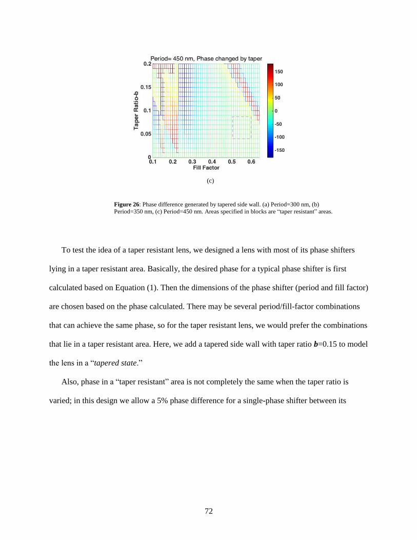
72
To test the idea of a taper resistant lens, we designed a lens with most of its phase shifters
lying in a taper resistant area. Basically, the desired phase for a typical phase shifter is first
calculated based on Equation (1). Then the dimensions of the phase shifter (period and fill factor)
are chosen based on the phase calculated. There may be several period/fill-factor combinations
that can achieve the same phase, so for the taper resistant lens, we would prefer the combinations
that lie in a taper resistant area. Here, we add a tapered side wall with taper ratio b=0.15 to model
the lens in a “tapered state.”
Also, phase in a “taper resistant” area is not completely the same when the taper ratio is
varied; in this design we allow a 5% phase difference for a single-phase shifter between its
(c)
Figure 26: Phase difference generated by tapered side wall. (a) Period=300 nm, (b)
Period=350 nm, (c) Period=450 nm. Areas specified in blocks are “taper resistant” areas.
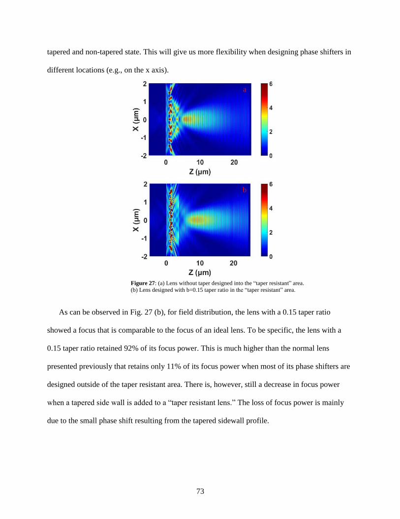
73
tapered and non-tapered state. This will give us more flexibility when designing phase shifters in
different locations (e.g., on the x axis).
As can be observed in Fig. 27 (b), for field distribution, the lens with a 0.15 taper ratio
showed a focus that is comparable to the focus of an ideal lens. To be specific, the lens with a
0.15 taper ratio retained 92% of its focus power. This is much higher than the normal lens
presented previously that retains only 11% of its focus power when most of its phase shifters are
designed outside of the taper resistant area. There is, however, still a decrease in focus power
when a tapered side wall is added to a “taper resistant lens.” The loss of focus power is mainly
due to the small phase shift resulting from the tapered sidewall profile.
a
b
Figure 27: (a) Lens without taper designed into the “taper resistant” area.
(b) Lens designed with b=0.15 taper ratio in the “taper resistant” area.
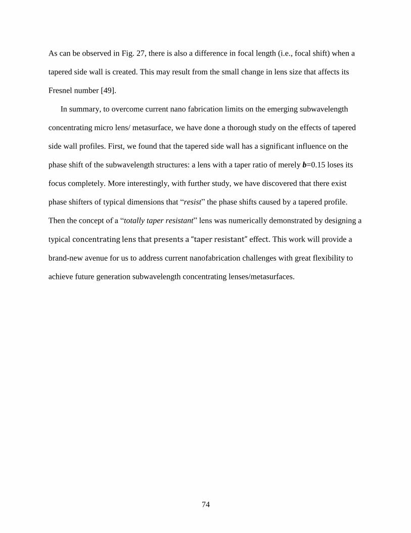
74
As can be observed in Fig. 27, there is also a difference in focal length (i.e., focal shift) when a
tapered side wall is created. This may result from the small change in lens size that affects its
Fresnel number [49].
In summary, to overcome current nano fabrication limits on the emerging subwavelength
concentrating micro lens/ metasurface, we have done a thorough study on the effects of tapered
side wall profiles. First, we found that the tapered side wall has a significant influence on the
phase shift of the subwavelength structures: a lens with a taper ratio of merely b=0.15 loses its
focus completely. More interestingly, with further study, we have discovered that there exist
phase shifters of typical dimensions that “resist” the phase shifts caused by a tapered profile.
Then the concept of a “totally taper resistant” lens was numerically demonstrated by designing a
typical concentrating lens that presents a “taper resistant” effect. This work will provide a
brand-new avenue for us to address current nanofabrication challenges with great flexibility to
achieve future generation subwavelength concentrating lenses/metasurfaces.
75
Chapter 10 Low Contrast Subwavelength Grating Lenses
Concentrating lens is one of the most important components for photovoltaics. The nano-scale
subwavelength grating structure has been investigated widely as it promises a series of
applications in integrated nanophotonics. Low contrast gratings, such as Zero-contrast gratings
(ZCG) based on guided-mode resonance (GMR) structures [50,51] and high-contrast grating
(HCG) [52, 53], were investigated as wideband reflectors. These types of subwavelength
structures have potential in many applications including optical filters [5], sensing [6, 7], and
photodetectors [8], offering flexible tunability of resonance wavelength and high Q factor. Until
recently, nanorod arrays (NRAs) with high aspect ratio has attracted wide attention for its
potential applications such as antireflection, self-cleaning and superhydrophobicity [54-57]. Dry
etching technique is one most favorable method due to its excellent controllability and
compatibility with the CMOS technology. Both vertical and transverse etching in most dry
etching processes, such as reactive-ion-etching (RIE) technique normally requires good control
of etching rate to achieve good selectivity over underneath thin film.
Based on coupled-wave diffraction method [13], various micro lenses has been designed,
from traditional dielectric lenses to plasmonic lenses [14]. Among all the micro lenses, sub-
wavelength structure designs based on recently proposed HCG structures [3, 4] has gained most
attention as it is compatible with planar CMOS integration process while has excellent light
focusing properties. However, the HCG structures normally requires the high index contrast at
the interface between the grating materials and the surrounding materials, this HCG structure
needs accurate control of thin film etching. Also, even though the design of high aspect ratio
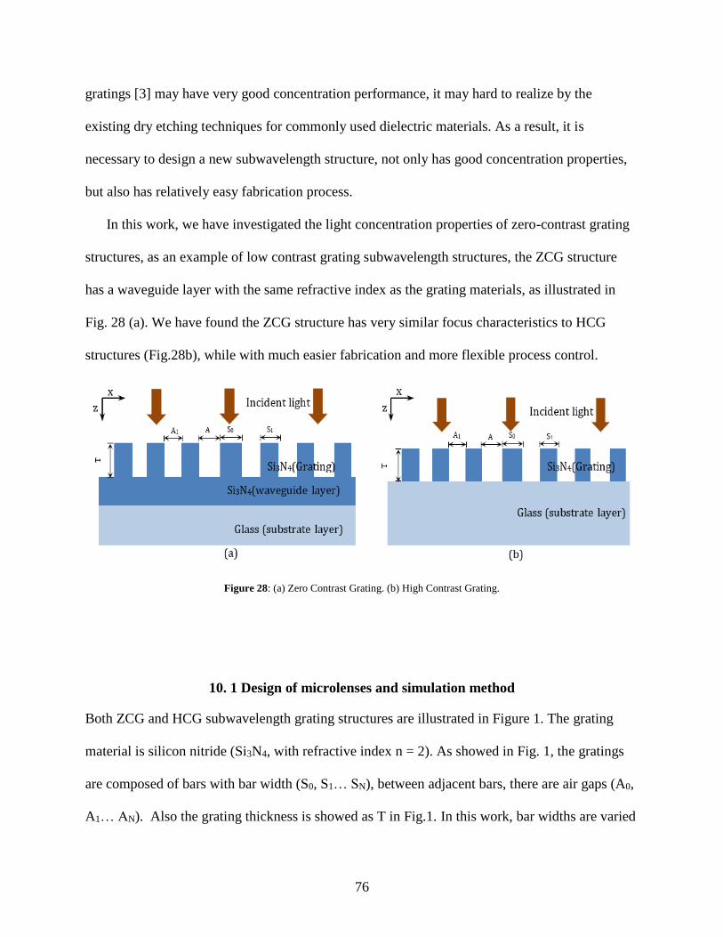
76
gratings [3] may have very good concentration performance, it may hard to realize by the
existing dry etching techniques for commonly used dielectric materials. As a result, it is
necessary to design a new subwavelength structure, not only has good concentration properties,
but also has relatively easy fabrication process.
In this work, we have investigated the light concentration properties of zero-contrast grating
structures, as an example of low contrast grating subwavelength structures, the ZCG structure
has a waveguide layer with the same refractive index as the grating materials, as illustrated in
Fig. 28 (a). We have found the ZCG structure has very similar focus characteristics to HCG
structures (Fig.28b), while with much easier fabrication and more flexible process control.
Figure 28: (a) Zero Contrast Grating. (b) High Contrast Grating.
10. 1 Design of microlenses and simulation method
Both ZCG and HCG subwavelength grating structures are illustrated in Figure 1. The grating
material is silicon nitride (Si3N4, with refractive index n = 2). As showed in Fig. 1, the gratings
are composed of bars with bar width (S0, S1… SN), between adjacent bars, there are air gaps (A0,
A1… AN). Also the grating thickness is showed as T in Fig.1. In this work, bar widths are varied
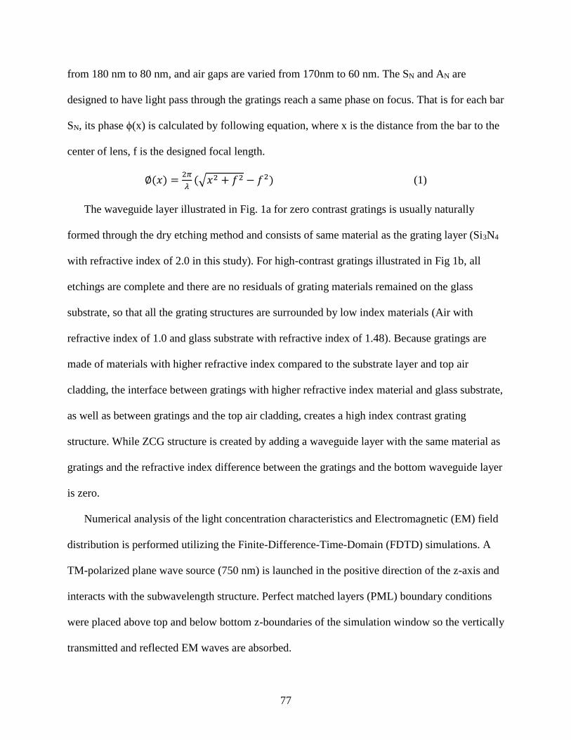
77
from 180 nm to 80 nm, and air gaps are varied from 170nm to 60 nm. The SN and AN are
designed to have light pass through the gratings reach a same phase on focus. That is for each bar
SN, its phase ϕ(x) is calculated by following equation, where x is the distance from the bar to the
center of lens, f is the designed focal length.
∅(𝑥) =2𝜋
𝜆(√𝑥2 + 𝑓2 − 𝑓2) (1)
The waveguide layer illustrated in Fig. 1a for zero contrast gratings is usually naturally
formed through the dry etching method and consists of same material as the grating layer (Si3N4
with refractive index of 2.0 in this study). For high-contrast gratings illustrated in Fig 1b, all
etchings are complete and there are no residuals of grating materials remained on the glass
substrate, so that all the grating structures are surrounded by low index materials (Air with
refractive index of 1.0 and glass substrate with refractive index of 1.48). Because gratings are
made of materials with higher refractive index compared to the substrate layer and top air
cladding, the interface between gratings with higher refractive index material and glass substrate,
as well as between gratings and the top air cladding, creates a high index contrast grating
structure. While ZCG structure is created by adding a waveguide layer with the same material as
gratings and the refractive index difference between the gratings and the bottom waveguide layer
is zero.
Numerical analysis of the light concentration characteristics and Electromagnetic (EM) field
distribution is performed utilizing the Finite-Difference-Time-Domain (FDTD) simulations. A
TM-polarized plane wave source (750 nm) is launched in the positive direction of the z-axis and
interacts with the subwavelength structure. Perfect matched layers (PML) boundary conditions
were placed above top and below bottom z-boundaries of the simulation window so the vertically
transmitted and reflected EM waves are absorbed.
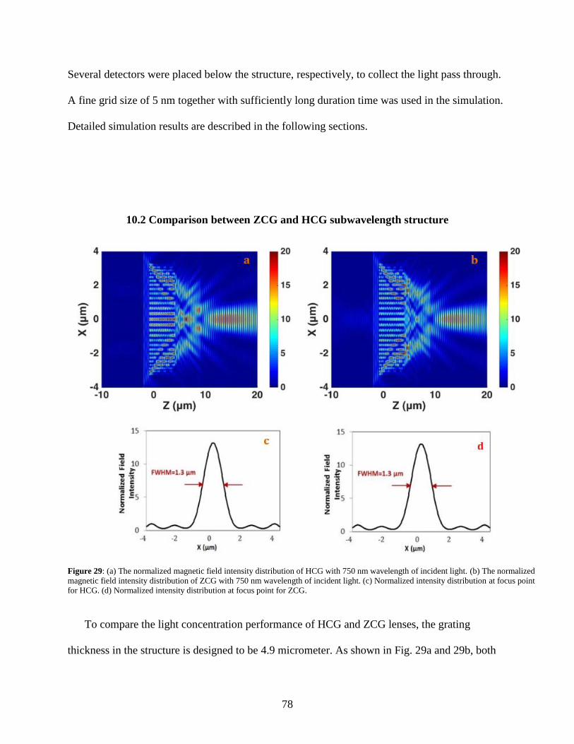
78
Several detectors were placed below the structure, respectively, to collect the light pass through.
A fine grid size of 5 nm together with sufficiently long duration time was used in the simulation.
Detailed simulation results are described in the following sections.
10.2 Comparison between ZCG and HCG subwavelength structure
To compare the light concentration performance of HCG and ZCG lenses, the grating
thickness in the structure is designed to be 4.9 micrometer. As shown in Fig. 29a and 29b, both
Figure 29: (a) The normalized magnetic field intensity distribution of HCG with 750 nm wavelength of incident light. (b) The normalized
magnetic field intensity distribution of ZCG with 750 nm wavelength of incident light. (c) Normalized intensity distribution at focus point
for HCG. (d) Normalized intensity distribution at focus point for ZCG.
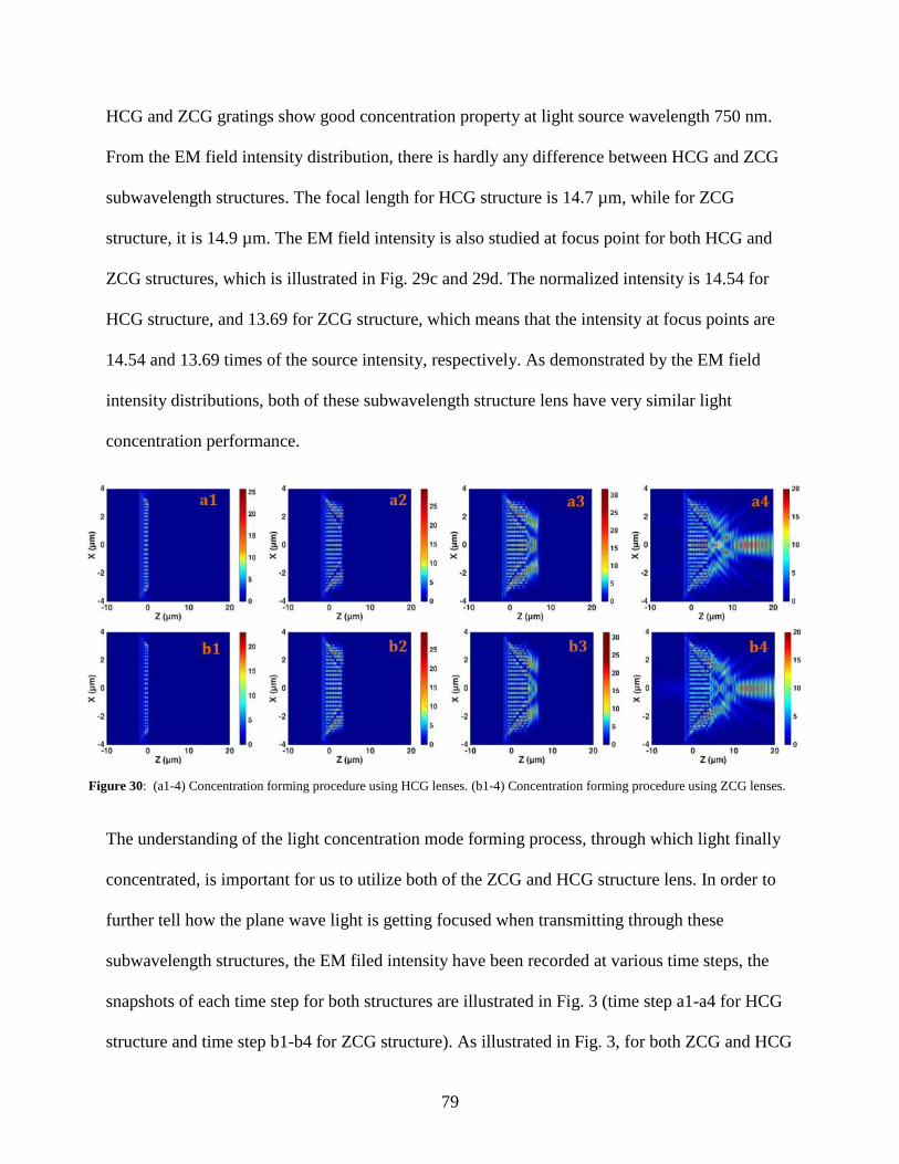
79
HCG and ZCG gratings show good concentration property at light source wavelength 750 nm.
From the EM field intensity distribution, there is hardly any difference between HCG and ZCG
subwavelength structures. The focal length for HCG structure is 14.7 µm, while for ZCG
structure, it is 14.9 µm. The EM field intensity is also studied at focus point for both HCG and
ZCG structures, which is illustrated in Fig. 29c and 29d. The normalized intensity is 14.54 for
HCG structure, and 13.69 for ZCG structure, which means that the intensity at focus points are
14.54 and 13.69 times of the source intensity, respectively. As demonstrated by the EM field
intensity distributions, both of these subwavelength structure lens have very similar light
concentration performance.
The understanding of the light concentration mode forming process, through which light finally
concentrated, is important for us to utilize both of the ZCG and HCG structure lens. In order to
further tell how the plane wave light is getting focused when transmitting through these
subwavelength structures, the EM filed intensity have been recorded at various time steps, the
snapshots of each time step for both structures are illustrated in Fig. 3 (time step a1-a4 for HCG
structure and time step b1-b4 for ZCG structure). As illustrated in Fig. 3, for both ZCG and HCG
Figure 30: (a1-4) Concentration forming procedure using HCG lenses. (b1-4) Concentration forming procedure using ZCG lenses.
80
structures, light is coupled into the gratings immediately when penetrating into the lenses, which
can be regarded as individual wave guiding mode. Due to the same refractive index of adjacent
grating bars, light inside the gratings are in almost the same phase along z direction. While for
each grating bar, the bar width is different and within the near-field coupling range, thus the
electromagnetic fields for each grating mode strongly interfere with each other along x direction.
As shown in Fig.3, during light propagation inside the gratings, the electromagnetic fields of
adjacent bars interfere with each other and form resonance mode patterns along the x direction.
The interference patterns of electromagnetic field along x direction finally result in concentration
effect. As can be observed from Fig. 3 (a1-a2) and (b1-b2), the light begins to bend once
coupling into gratings on air/grating interface. It can be reasoned that the interference of
electromagnetic fields is happening once the light is interacting with the grating structures. As
long as the bar width is fixed, the interference pattern of electromagnetic fields is then
determined. So from the snapshots of both HCG and ZCG structures at different time step, the
concentration process can be described as: a) The interference patterns is formed by the
interference of coupled grating bar modes. b) The resonance modes propagate along the z
direction while interfering with each other. c) A light concentration is finally formed with at the
focus point.
From the light concentration formation mechanism described above, it can be inferred that
the existence of waveguide layer hardly affects the coupled resonance mode interference of
electromagnetic field, which explains the minor difference of concentration performance
between HCG and ZCG subwavelength grating structures. In addition, TE polarized source is
also utilized in simulation which results in similar EM field distribution, both ZCG and HCG
lenses have concentration properties with focal length difference less than 0.1 µm. This is also
81
because the concentration effect is resulted from the interference of coupled resonance modes
within the gratings. Polarization seems doesn’t show observable effects.
While the light concentration is mainly trapped in the gratings; for HCG, there is a small
portion of light reflected on the grating/substrate surface which directly interacted with
themselves and possibly lowered the focus intensity. This might be why HCG had a little bit
smaller intensity at focus point.
In terms of fabrication process, compared to ZCG structure, complete HCG structure is
relatively more challenging to fabricate based on current nano fabrication techniques due to the
need to accurately control the etch stop during etching process. As mentioned above, the main
difference between the HCG and ZCG structure is the insertion of the same material waveguide
layer. In the following section, we have also investigated the ZCG structure by varying the
thickness of the waveguide layer to see how the thickness of waveguide layer may affect light
concentration properties.
10.3 Effect of thickness of waveguide layer
In this section, the grating thickness is kept at 400 nm to maintain a relatively low aspect ratio,
which is in consistent with the conventional nano fabrication techniques.
When we vary the thickness of waveguide layer from 0.5 µm, 1 µm to 2 µm, the focal length
is 21.5 µm, 21.6 µm, and 21.9 µm, respectively, which has a very small difference among the
above three cases. The peak intensity is 11.58, 11.57, and 11.81 respectively, as illustrated in
Fig. 31 (a-c). This results confirms what we have observed in the above section that the light
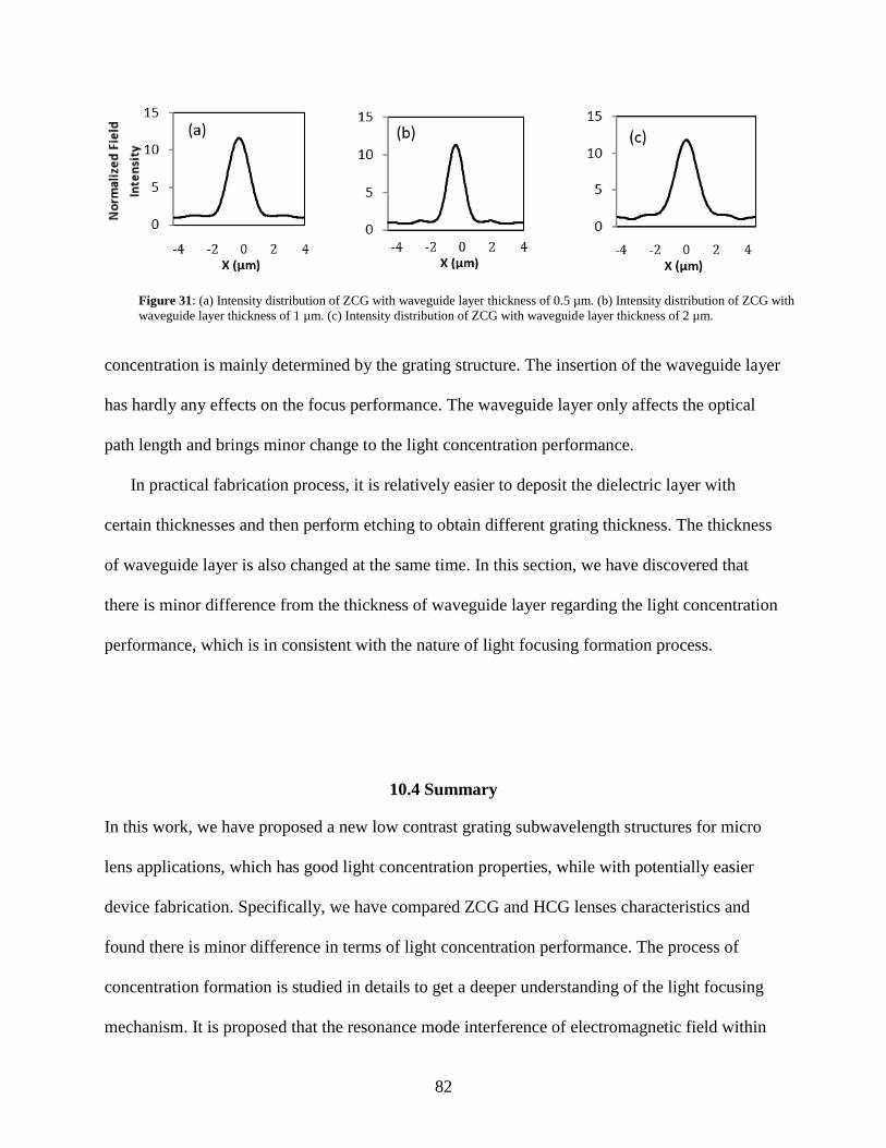
82
concentration is mainly determined by the grating structure. The insertion of the waveguide layer
has hardly any effects on the focus performance. The waveguide layer only affects the optical
path length and brings minor change to the light concentration performance.
In practical fabrication process, it is relatively easier to deposit the dielectric layer with
certain thicknesses and then perform etching to obtain different grating thickness. The thickness
of waveguide layer is also changed at the same time. In this section, we have discovered that
there is minor difference from the thickness of waveguide layer regarding the light concentration
performance, which is in consistent with the nature of light focusing formation process.
10.4 Summary
In this work, we have proposed a new low contrast grating subwavelength structures for micro
lens applications, which has good light concentration properties, while with potentially easier
device fabrication. Specifically, we have compared ZCG and HCG lenses characteristics and
found there is minor difference in terms of light concentration performance. The process of
concentration formation is studied in details to get a deeper understanding of the light focusing
mechanism. It is proposed that the resonance mode interference of electromagnetic field within
Figure 31: (a) Intensity distribution of ZCG with waveguide layer thickness of 0.5 µm. (b) Intensity distribution of ZCG with
waveguide layer thickness of 1 µm. (c) Intensity distribution of ZCG with waveguide layer thickness of 2 µm.

83
the grating structures along the grating direction is the main factor to determine the light
concentration properties.
For ZCG subwavelength structures, when taking into account the conventional nano
fabrication technique, the effect of thickness of waveguide layer and grating layer is also studied,
and it is found that the thickness of waveguide layer hardly affects the light concentration
performance. Our work will be promising for a series of potential applications in integrated
nanophotonics field, such as imaging, display, photo detection and concentrating photovoltaics.

84
Chapter 11 Influence of Grating Thickness in Low Contrast Subwavelengths Grating
Concentrating Lenses
Grating thickness is one of the most important parameters in the subwavelength grating structures.
Here, we have explored the effects of grating thickness on focus properties by taking into account
the practical ZCG lens fabrication process. The fabrication of the subwavelength grating structure
starts from a thin dielectric film and is then etched to a certain depth to obtain the grating structure.
It is important to study how the grating thickness affects the light concentration performance to
optimize tradeoff between the concentration performance and fabrication limitation.
In this section we assume a practical fabrication condition: a 2 µm silicon nitride layer is first
deposited on the glass substrate, and then etched down to certain depths to create the grating
structure with 100 nm, 200 nm, 400 nm, 600 nm, 800 nm and 1000 nm of grating thicknesses. This
results in the thickness of each waveguide layer to be 1.9 µm, 1.8 µm, 1.6 µm, 1.4 µm, 1.2 µm and
1 µm, respectively. It is widely acknowledged that the concentration property depends on the
structure of gratings; the difference waveguide layer thickness has negligible effect on its focus
property. For our study, we vary the etching depth of the silicon nitride to create different grating
thicknesses while keeping all other structure parameters the same.
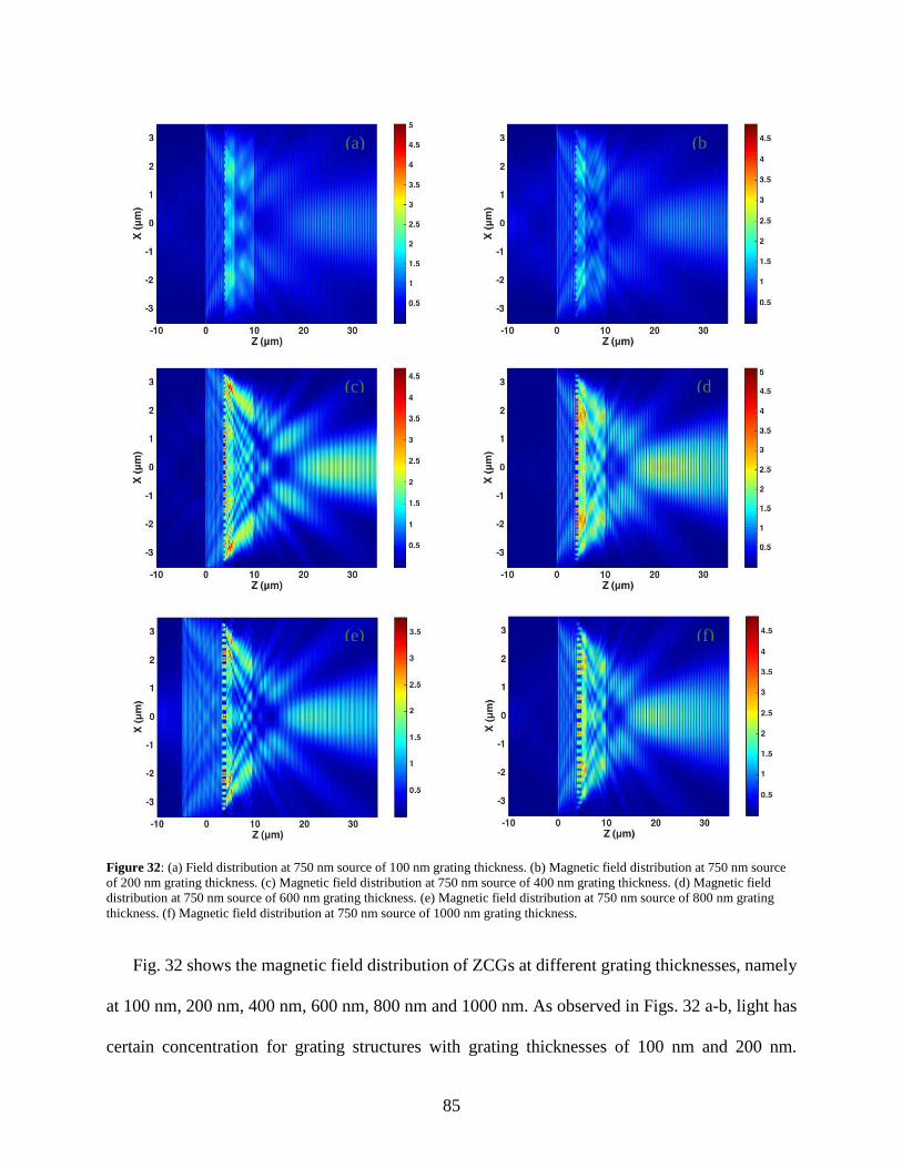
85
Figure 32: (a) Field distribution at 750 nm source of 100 nm grating thickness. (b) Magnetic field distribution at 750 nm source
of 200 nm grating thickness. (c) Magnetic field distribution at 750 nm source of 400 nm grating thickness. (d) Magnetic field
distribution at 750 nm source of 600 nm grating thickness. (e) Magnetic field distribution at 750 nm source of 800 nm grating
thickness. (f) Magnetic field distribution at 750 nm source of 1000 nm grating thickness.
Fig. 32 shows the magnetic field distribution of ZCGs at different grating thicknesses, namely
at 100 nm, 200 nm, 400 nm, 600 nm, 800 nm and 1000 nm. As observed in Figs. 32 a-b, light has
certain concentration for grating structures with grating thicknesses of 100 nm and 200 nm.
(a) (b
(c) (d
(e) (f)
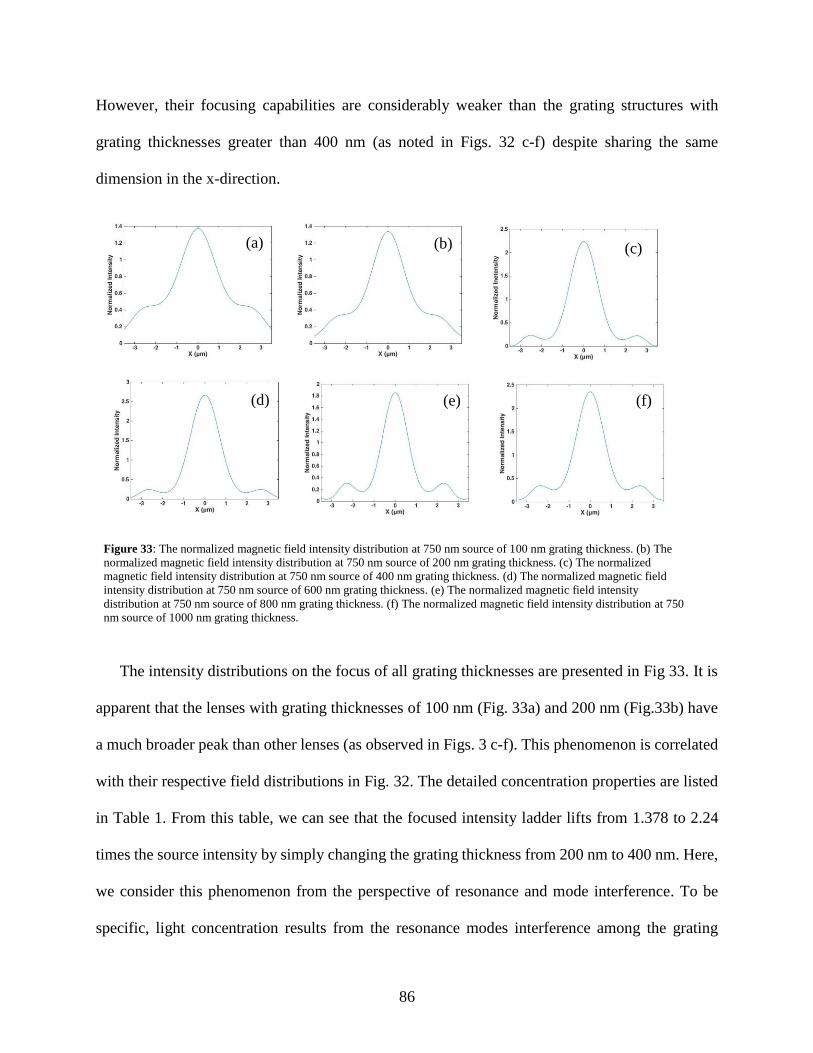
86
However, their focusing capabilities are considerably weaker than the grating structures with
grating thicknesses greater than 400 nm (as noted in Figs. 32 c-f) despite sharing the same
dimension in the x-direction.
The intensity distributions on the focus of all grating thicknesses are presented in Fig 33. It is
apparent that the lenses with grating thicknesses of 100 nm (Fig. 33a) and 200 nm (Fig.33b) have
a much broader peak than other lenses (as observed in Figs. 3 c-f). This phenomenon is correlated
with their respective field distributions in Fig. 32. The detailed concentration properties are listed
in Table 1. From this table, we can see that the focused intensity ladder lifts from 1.378 to 2.24
times the source intensity by simply changing the grating thickness from 200 nm to 400 nm. Here,
we consider this phenomenon from the perspective of resonance and mode interference. To be
specific, light concentration results from the resonance modes interference among the grating
(a) (b) (c)
(d) (e) (f)
Figure 33: The normalized magnetic field intensity distribution at 750 nm source of 100 nm grating thickness. (b) The
normalized magnetic field intensity distribution at 750 nm source of 200 nm grating thickness. (c) The normalized
magnetic field intensity distribution at 750 nm source of 400 nm grating thickness. (d) The normalized magnetic field
intensity distribution at 750 nm source of 600 nm grating thickness. (e) The normalized magnetic field intensity
distribution at 750 nm source of 800 nm grating thickness. (f) The normalized magnetic field intensity distribution at 750
nm source of 1000 nm grating thickness.
87
structures (i.e. electromagnetic field interference of grating bars). When the grating thickness is
less than 200 nm, which is much smaller than half the wavelength of our light source (750 nm), a
complete concentration resonance mode cannot be formed before the light reaches the waveguide
layer. For lenses with grating thickness higher than 200 nm, the difference in focus intensity is not
as significant since the optical path length in the z-direction allows at least one cycle of
electromagnetic field interference along the x-direction.
However, the focus intensity does not continuously increase with incremental changes of the
grating thicknesses. If we compare the focused peak intensity of gratings with 600 nm and 800 nm
thicknesses, a drop from 2.666 to 1.855 times the incident light intensity is observed. This change
in intensity indicates the existence of resonance mode self-interference in the z-direction.
Specifically, the concentration resonance modes propagate to the waveguide layer after they are
created. A ZCG structure with 800 nm grating thickness has a waveguide layer of 1.2 µm, which
is close to the odd multiples (3 times) of the half source-wavelengths. In this typical case, the
concentration resonance mode experienced a strong interference with the reflection mode
generated at the interface of the waveguide and substrate layer. This negative interference
diminished the magnitude concentration resonance mode and resulted in the observed drop in the
focus intensity.
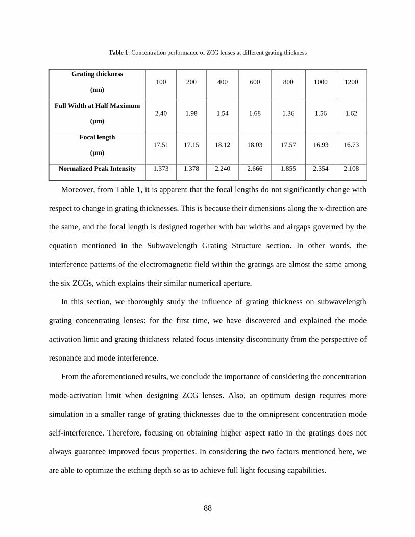
88
Table 1: Concentration performance of ZCG lenses at different grating thickness
Grating thickness
(nm)
100 200 400 600 800 1000 1200
Full Width at Half Maximum
(µm)
2.40 1.98 1.54 1.68 1.36 1.56 1.62
Focal length
(µm)
17.51 17.15 18.12 18.03 17.57 16.93 16.73
Normalized Peak Intensity 1.373 1.378 2.240 2.666 1.855 2.354 2.108
Moreover, from Table 1, it is apparent that the focal lengths do not significantly change with
respect to change in grating thicknesses. This is because their dimensions along the x-direction are
the same, and the focal length is designed together with bar widths and airgaps governed by the
equation mentioned in the Subwavelength Grating Structure section. In other words, the
interference patterns of the electromagnetic field within the gratings are almost the same among
the six ZCGs, which explains their similar numerical aperture.
In this section, we thoroughly study the influence of grating thickness on subwavelength
grating concentrating lenses: for the first time, we have discovered and explained the mode
activation limit and grating thickness related focus intensity discontinuity from the perspective of
resonance and mode interference.
From the aforementioned results, we conclude the importance of considering the concentration
mode-activation limit when designing ZCG lenses. Also, an optimum design requires more
simulation in a smaller range of grating thicknesses due to the omnipresent concentration mode
self-interference. Therefore, focusing on obtaining higher aspect ratio in the gratings does not
always guarantee improved focus properties. In considering the two factors mentioned here, we
are able to optimize the etching depth so as to achieve full light focusing capabilities.

89
11.1 Summary
This study on the influence of the grating thickness on subwavelength grating concentrating lenses
is proposed for the first time. The thickness of grating is taken as an isolated parameter in
determining the focusing characteristics within a fabrication range, and two major discoveries were
made:
• A concentration mode-activation limit exists for grating thickness that causes the focus
intensity to spike upon exceeding this threshold.
• There exists a concentration mode self-interference effect along light propagation direction
which prevents the focus intensity from increasing continuously with incremental change
in grating thickness.
Previous works primarily focus on phase differences to study the design and focus property of
subwavelength concentrating grating lenses. Determination of the grating thickness has long been
believed to be a decision correlated with other dimensions (i.e. bar width and airgap) to calculate
the phase differences. In this work, we have explained the underlying principle of mode activation
limit and concentration mode self-interference in different perspective of resonance and mode
interference. It is noted that these two discoveries are unique and the first of their kind.
Our work has the potential to provide guidance in improving the design of numerous devices
in the field of integrated nanophotonics, such as imaging, display, photo detection and
concentrating photovoltaics.
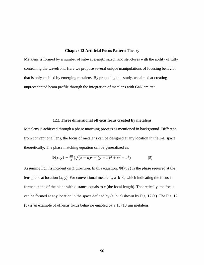
90
Chapter 12 Artificial Focus Pattern Theory
Metalens is formed by a number of subwavelength sized nano structures with the ability of fully
controlling the wavefront. Here we propose several unique manipulations of focusing behavior
that is only enabled by emerging metalens. By proposing this study, we aimed at creating
unprecedented beam profile through the integration of metalens with GaN emitter.
12.1 Three dimensional off-axis focus created by metalens
Metalens is achieved through a phase matching process as mentioned in background. Different
from conventional lens, the focus of metalens can be designed at any location in the 3-D space
theoretically. The phase matching equation can be generalized as:
Ф(𝑥, 𝑦) =2𝜋
𝜆(√(𝑥 − 𝑎)2 + (𝑦 − 𝑏)2 + 𝑐2 − 𝑐2) (5)
Assuming light is incident on Z direction. In this equation, Ф(𝑥, 𝑦) is the phase required at the
lens plane at location (x, y). For conventional metalens, a=b=0, which indicating the focus is
formed at the of the plane with distance equals to c (the focal length). Theoretically, the focus
can be formed at any location in the space defined by (a, b, c) shown by Fig. 12 (a). The Fig. 12
(b) is an example of off-axis focus behavior enabled by a 13×13 µm metalens.
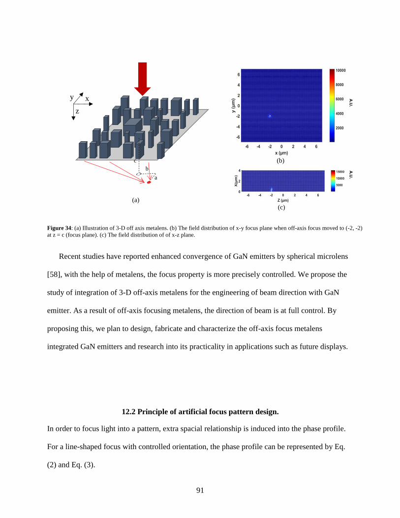
91
Recent studies have reported enhanced convergence of GaN emitters by spherical microlens
[58], with the help of metalens, the focus property is more precisely controlled. We propose the
study of integration of 3-D off-axis metalens for the engineering of beam direction with GaN
emitter. As a result of off-axis focusing metalens, the direction of beam is at full control. By
proposing this, we plan to design, fabricate and characterize the off-axis focus metalens
integrated GaN emitters and research into its practicality in applications such as future displays.
12.2 Principle of artificial focus pattern design.
In order to focus light into a pattern, extra spacial relationship is induced into the phase profile.
For a line-shaped focus with controlled orientation, the phase profile can be represented by Eq.
(2) and Eq. (3).
x y
z
c
b
a
(a)
(b)
Figure 34: (a) Illustration of 3-D off axis metalens. (b) The field distribution of x-y focus plane when off-axis focus moved to (-2, -2)
at z = c (focus plane). (c) The field distribution of of x-z plane.
(c)
92
ϕ(𝑥, 𝑦) − ϕ(0,0) =2𝜋
𝜆(√(𝑥 + 𝑎(𝑦))2 + 𝑓2 − 𝑓) (2)
−𝑎(𝑦) =𝑦−𝑐
𝑘 (3)
Where k and c are the slope and spacial constant of line-shaped focus at x-y focal plane, a(y) is a
function of the coordinate y (Fig.35 A). Basically, Eq (2) is creating focus with off-axis
parameter a(y) and this parameter is a function of coordinate y. An example of line-shaped focus
created by combining Eq. 3 and Eq. 4 is shown in Fig. 1 (B) where k=-2, c=0. The metalens is
designed through propagation phase with cylindrical shaped nano structure (Fig. 35 A) with size
of 10×10 µm and focal length of 6 µm, and filed distribution is calculated through finite
difference time domain (FDTD) method, Fig. 2 (B) is the filed distribution on the designed focal
plane.
We can intuitively understand this focus pattern as a result of ‘overlapping’ of multiple
focuses. To be specific, based on Eq. (3), the function a(y) is varied based on the y coordinate of
C
Focus overlapping failed
Incident
Focus
A
B
D
High |a(y)|
Inten
sity (a. u.)
Inten
sity (a. u.)
k
Micro focus
Center of micro
|a(y+U)-
U
c
Figure 35: Design and discussion of line-shaped focus pattern. (A) Schematic graph of design method of line-shaped focus. (B) FDTD
simulation of typical example of line-shaped focus by combining Eq. (2) and Eq. (3) with k=-2, c=0. (C) Illustration of ‘micro focus
93
the phase shifter, thus we can consider phase shifters with same y coordinate (e.g. each line of
phase shifters) as a ‘micro metalens’. These metalens generate off-axis focus based on the value
of a(y). Due to close distance between adjacent focuses, these focuses become overlapped and
form continuous pattern, which is shown in Fig. 35 (C). The distance between adjacent ‘micro
focus’ is shown by
𝐷(𝑦) = √(𝑎(𝑦 + 𝑈) − 𝑎(𝑦))2 + 𝑈2 ≤𝜆
2𝑁𝐴(𝑦) (4)
Where U (220 nm) and NA(y) are pitch (period) size and numerical aperture, D(y) is the distance
between adjacent ‘micro focus’ created by adjacent ‘micro metalenses’. Note that the NA(y) in
Eq. (5) is the numerical aperture of the typical ‘micro metalens’, which is also a variable of y
coordinate. And due to the diffraction limited size of ‘micro focus’, D(y) has to be smaller than
the Abby’s diffraction limit.
With this approach, we are able to create line-shaped focus across the focal plane. While, as
we discovered, simply engineering a(y) (Eq. 3) will not render desired focus pattern even when
the criterion of Eq. (4) is fulfilled. To better illustrate this issue, we have designed an arc-shaped
focus by modifying Eq. (3) to
−𝑎(𝑦) = √𝑟2 − y2 (5)
Where r (10 µm) is the radius of the arc. This metalens is designed under same size (10×10 µm)
and focal length (6 µm). The field distribution at focal plane is shown in Fig. 1 (D). In this
example, the distance between adjacent focuses D(y) increased due to the increase of y
coordinate, that the arc structure disappeared at y > 6 µm due to dissatisfaction of Eq. 5.
However, counterintuitively, the intensity of arc is does not follows an inverse relationship with
D(y). To be specific, the intensity of artificial focus pattern is closely related to D(y), as smaller
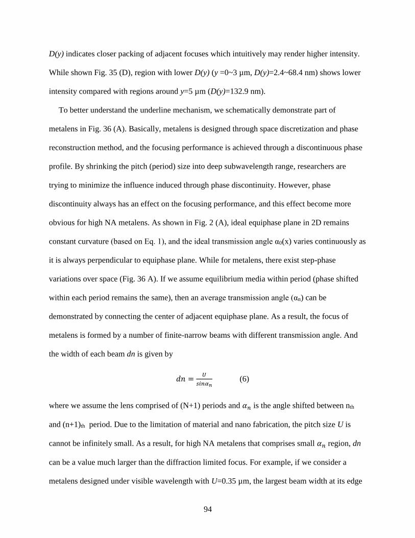
94
D(y) indicates closer packing of adjacent focuses which intuitively may render higher intensity.
While shown Fig. 35 (D), region with lower D(y) (y =0~3 µm, D(y)=2.4~68.4 nm) shows lower
intensity compared with regions around y=5 µm (D(y)=132.9 nm).
To better understand the underline mechanism, we schematically demonstrate part of
metalens in Fig. 36 (A). Basically, metalens is designed through space discretization and phase
reconstruction method, and the focusing performance is achieved through a discontinuous phase
profile. By shrinking the pitch (period) size into deep subwavelength range, researchers are
trying to minimize the influence induced through phase discontinuity. However, phase
discontinuity always has an effect on the focusing performance, and this effect become more
obvious for high NA metalens. As shown in Fig. 2 (A), ideal equiphase plane in 2D remains
constant curvature (based on Eq. 1), and the ideal transmission angle α0(x) varies continuously as
it is always perpendicular to equiphase plane. While for metalens, there exist step-phase
variations over space (Fig. 36 A). If we assume equilibrium media within period (phase shifted
within each period remains the same), then an average transmission angle (αn) can be
demonstrated by connecting the center of adjacent equiphase plane. As a result, the focus of
metalens is formed by a number of finite-narrow beams with different transmission angle. And
the width of each beam dn is given by
𝑑𝑛 =𝑈
𝑠𝑖𝑛𝛼𝑛 (6)
where we assume the lens comprised of (N+1) periods and 𝛼𝑛 is the angle shifted between nth
and (n+1)th period. Due to the limitation of material and nano fabrication, the pitch size U is
cannot be infinitely small. As a result, for high NA metalens that comprises small 𝛼𝑛 region, dn
can be a value much larger than the diffraction limited focus. For example, if we consider a
metalens designed under visible wavelength with U=0.35 µm, the largest beam width at its edge
95
for NA=0.9 can render dN=0.802 µm, and it reaches dN=2.48 µm at NA=0.99. Large dn may
render a much larger focus with decreased intensity depicted at Fig. 2 (B).
A metalens with off-axis focus can be considered as a combination of two metalens with
different NA and same focal length as shown in Fig. 36 (C). Due to the increasing value of dn,
beam come from high NA part is concentrated to a larger area, which increased the size of focus
and bring a decrease to focused power.
In our artificial focus pattern design, the focus is formed by a series of off-axis ‘micro focus’.
For focus generated with large |a(y)|, there exist a high NA part of metalens which rendered the
effect depicted in Fig. 2 (C) (e.g. the focused power is reduced for ‘micro metalens’ comprised
of large |a(y)| component). And this explained the issue we aforementioned for the arc-shaped
focus (Fig. 35 D) where lower D(y) rendered lower focused power.
Basically, the diminishing of focus power problems are inherent drawbacks of space
discretization, which can only be significantly improved when the pitch sized is reduced [13]. In
addition, based on the mechanism discussed in Fig. 36, the focused intensity is varying as a
function of a(y). However, for the design of artificial focus pattern, it is important to maintain
features with similar focused intensity across the whole pattern. In this application, we modified
the Eq. (2) to
ϕ(𝑥, 𝑦) − ϕ(0,0) =2𝜋
𝜆(√(𝑥 + 𝑎(𝑦))2 + (𝑓 + 𝑠(𝑦))2 − (𝑓 + 𝑠(𝑦))) (8)
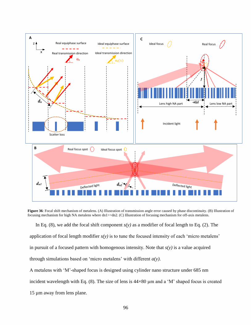
96
In Eq. (8), we add the focal shift component s(y) as a modifier of focal length to Eq. (2). The
application of focal length modifier s(y) is to tune the focused intensity of each ‘micro metalens’
in pursuit of a focused pattern with homogenous intensity. Note that s(y) is a value acquired
through simulations based on ‘micro metalens’ with different a(y).
A metalens with ‘M’-shaped focus is designed using cylinder nano structure under 685 nm
incident wavelength with Eq. (8). The size of lens is 44×80 µm and a ‘M’ shaped focus is created
15 µm away from lens plane.
αn α0(x)
dn
Incident light
C Ideal equiphase surface Real equiphase surface
Scatter loss
Ideal transmission direction Real transmission direction
A
-a(y)
f
Lens high NA part Lens low NA part
Ideal focus Real focus
Ideal focus spot Real focus spot B
dn2
x
z
Figure 36: Focal shift mechanism of metalens. (A) Illustration of transmission angle error caused by phase discontinuity. (B) Illustration of
focusing mechanism for high NA metalens where dn1>>dn2. (C) Illustration of focusing mechanism for off-axis metalens.
97
The structure of lens is shown in Fig. 37 (A) and (B). The characterized focus pattern is
shown in Fig. 37 (C). The focus profile at two different lines of ‘M’ structure is shown in Fig. 37
(D). Basically, a clear ‘M’ shaped focus is formed at the designed focal plane, one side line of
‘M’ is blur which may cause by defects of nano fabrication. As can be observed in Fig. 3 (B) that
some of the cylinder is interconnected.
Shown by Fig. 37 (C), the tilted line of ‘M’ exhibits a similar brightness along its structure
which indicating that ‘micro focus’ created by varying a(y) is aligned to one focal plane. The
focus profile at position f1 and f2 in Fig. 37 (C) is shown at Fig. 37 (D), these focuses are
diffraction limited.
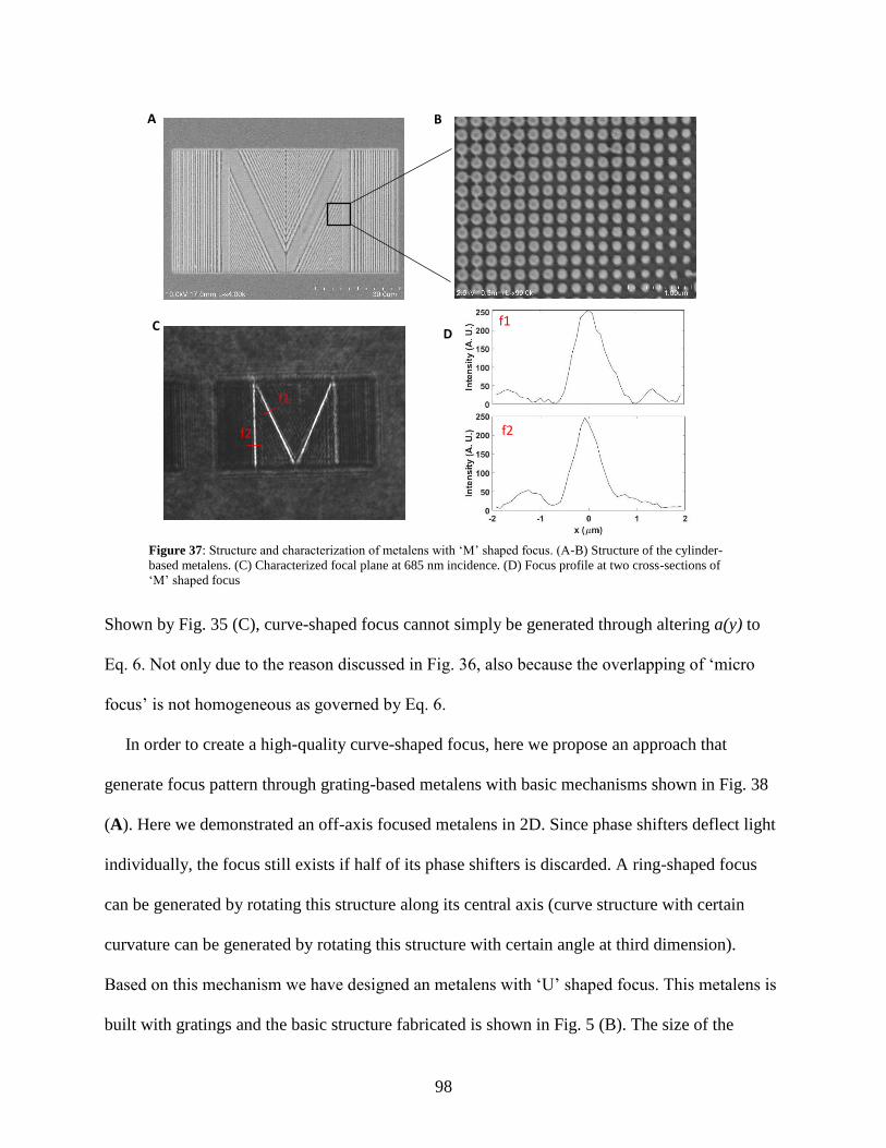
98
Shown by Fig. 35 (C), curve-shaped focus cannot simply be generated through altering a(y) to
Eq. 6. Not only due to the reason discussed in Fig. 36, also because the overlapping of ‘micro
focus’ is not homogeneous as governed by Eq. 6.
In order to create a high-quality curve-shaped focus, here we propose an approach that
generate focus pattern through grating-based metalens with basic mechanisms shown in Fig. 38
(A). Here we demonstrated an off-axis focused metalens in 2D. Since phase shifters deflect light
individually, the focus still exists if half of its phase shifters is discarded. A ring-shaped focus
can be generated by rotating this structure along its central axis (curve structure with certain
curvature can be generated by rotating this structure with certain angle at third dimension).
Based on this mechanism we have designed an metalens with ‘U’ shaped focus. This metalens is
built with gratings and the basic structure fabricated is shown in Fig. 5 (B). The size of the
B A
C
f1
f2
D
Figure 37: Structure and characterization of metalens with ‘M’ shaped focus. (A-B) Structure of the cylinder-
based metalens. (C) Characterized focal plane at 685 nm incidence. (D) Focus profile at two cross-sections of
‘M’ shaped focus
f1
f2
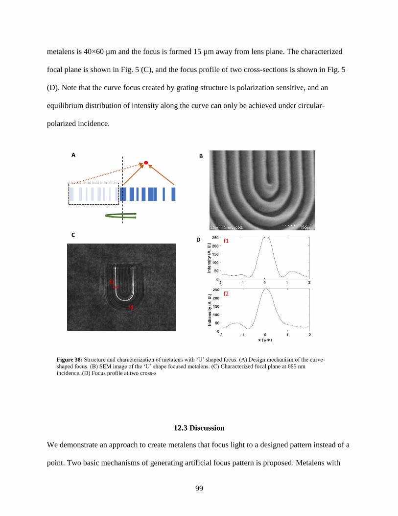
99
metalens is 40×60 µm and the focus is formed 15 µm away from lens plane. The characterized
focal plane is shown in Fig. 5 (C), and the focus profile of two cross-sections is shown in Fig. 5
(D). Note that the curve focus created by grating structure is polarization sensitive, and an
equilibrium distribution of intensity along the curve can only be achieved under circular-
polarized incidence.
12.3 Discussion
We demonstrate an approach to create metalens that focus light to a designed pattern instead of a
point. Two basic mechanisms of generating artificial focus pattern is proposed. Metalens with
A B
C D
f4
f3
f1
f2
Figure 38: Structure and characterization of metalens with ‘U’ shaped focus. (A) Design mechanism of the curve-
shaped focus. (B) SEM image of the ‘U’ shape focused metalens. (C) Characterized focal plane at 685 nm
incidence. (D) Focus profile at two cross-s

100
‘M’, ‘U’ shaped focus is fabricated and characterized for the proof of concept. During our study,
we discovered that metalens’ inherent phase discontinuity has major influence on the
performance of focus pattern. This result in the modification of phase construction equation with
space-variant focal length modifier in pursuit of homogeneous focus intensity. Eq. 8 is an
example of achieving line focus pattern, but the idea of overlapping multiple ‘micro focus’ to
generate focus pattern can be applied to various design as long as the requirements mentioned is
fulfilled.
Lens with artificial focus pattern can potentially benefit a plethora of applications that
involves beam engineering. A wide range of pattern can be generated by combination of basic
elements as ‘point’, ‘line’ and ‘curve’ that brings extra degrees of flexibility to beam shaping. In
addition, due to the large energy density that concentrated to the pattern, metalens of this kind
can potentially be applied to lithography with targeting pattern imprinted on the lens.
Even though the phase shifter we applied for ‘M’ patterned focus is cylinder-shaped, which in
many cases is considered as polarization-insensitive [11], there still exist difference in incident
polarization due to the anisotropic discretization of pitch (period). And the grating based
artificial focus pattern is polarization dependent, due to major phase difference under different
incident polarization.
Both design we demonstrated are based on the engineering of propagation phase through
modification of effective index within each period. Similar design can also be achieved through
Pancharatnam-Berry phase shifters. Even though this study is based on single wavelength,
strategies for achromatic metalens design can also be applied to the phase shifters which may
render achromatic artificial focus pattern.
101
References
1. F. Lu, F. G. Sedgwick, V. Karagodsky, C. Chase, C. J. Chang-Hasnain. Planar high-numerical-
aperture low-loss focusing reflectors and lenses using subwavelength high contrast gratings.
Opt. Express 18, 12606-12614 (2010).
2. D. Fattal, J. Li, Z. Peng, M. Fiorentino, R. G. Beausoleil. Flat dielectric grating reflectors with
focusing abilities. Nature Photonics 4, 466-470 (2011).
3. A. She, S. Zhang, S. Shian, D. R. Clarke, and F. Capasso, “Large area metalenses: design,
characterization, and mass manufacturing,” Optics Express, 26(2), 1573-1585 (2018).
4. M. Ye and Y. Yi, “Subwavelength grating microlens with taper-resistant characteristics,”,
Optics Letters, 42(6), 1031-1034 (2017).
5. M. Ye and Y. Yi, “Influence of grating thickness in low-contrast subwavelength grating
concentrating lenses,” Optical Engineering, 55(7), 075102 (2016).
6. M. Ye, X. Guo, and Y. Yi, “Transmission enhancement of subwavelength grating microlens
by tapered nanostructure,” MRS communication, 8(2), 509-513 (2018).
7. S. M. Kamali, E. Arbabi, A. Arbabi, and A. Faraon, “A review of dielectric optical
metasurfaces for wavefront control,” Nanophotonics, DOI: doi.org/10.1515/nanoph-2017-
0129 (2018).
8. S. Wang, P. C. Wu, V. Su, Y. Lai, M. Chen, H. Y. Kuo, Y. H. Chen, T. Huang, J. Wang, R.
Lin, C. Kuan, T. Li, Z. Wang, S. Zhu and D. P. Tsai, “A broadband achromatic metalens in the
visible,” Nature Nanotechnology, DOI: 10.1038/s41565-017-0052-4 (2018).
9. W. T. Chen, A. Y. Zhu, V. Sanjeev, M. Khorasaninejad, Z. Shi, E. Lee, and F. Capasso, “A
broadband achromatic metalens for focusing and imaging in the visible,” Nature
Nanotechnology, DOI: 10.1038/s41565-017-0034-6 (2018).
10. M. Ye, V. Ray, and Y. Yi, “Achromatic Flat Subwavelength Grating Lens Over Whole Visible
Bandwidths,” IEEE Photonics Technology Letters, 30(10), 955-958 (2018).
11. B. Chen, P. Wu, V. Su, Y. Lai, C. Chu, I. Lee, J. Chen, Y. Chen, Y. Lan, C. Kuan, and D. P.
Tsai, “GaN metalens for pixel-level full-color routing at visible light,” Nano Letters, 17(10),
6345-6352 (2017).
12. M. Tien, J. Bauters, M. Heck, D. Blumenthal, and J. Bowers, “Ultra-low loss Si3N4
waveguides with low nonlinearity and high power handling capability,” Optics Express, 18,
23562-23568 (2010).
13. Z. Fan, Z. Shao, M. Xie, X. Pang, W. Ruan, F. Zhao, Y. Chen, and S. Yu, J. Dong, “Silicon
Nitride Metalenses for Close-to-One Numerical Aperture and Wide-Angle Visible Imaging,”
Phys. Rev., 10, 014005 (2018).
14. M. A. Signore, A. Sytchkova, D. Dimaio, A. Cappello, and A. Rizzo, “Deposition of silicon
nitride thin films by RF magnetron sputtering: a material and growth process study,” Optical
Materials, 34, 632-638 (2012).
15. H. Huang, K. J. Winchester, A. Suvorova, B. R. Lawn, Y. Liu, X. Z. Hu, J. M. Dell, and L.
Faraone, “Effect of deposition conditions on mechanical properties of low-temperature
PECVD silicon nitride films,” Materials Science and Engineering: A, 435, 453-459 (2006).
16. M. Khorasaninejad, A. Y. Zhu, C. Roques-Carmes, W. T. Chen, J. Oh, I. Mishra, R. C. Devlin
and F. Capasso, “Polarization-intensive metalenses at visible wavelengths,” Nano Letters, 16,
7279-7234 (2016).
17. M. Khorasaninejad, W. T. Chen, R. C. Devlin, J. Oh, A. Y. Zhu, F. Capasso. Metalenses at
visible wavelengths: Diffraction-limited focusing and subwavelength resolution imaging.
Science 352, 1190-1194 (2016).
102
18. J. Mueller, N. Rubin, R. Devlin, B. Groever, F. Capasso. Metasurface Polarization Optics:
Independent Phase Control of Arbitrary Orthogonal States of Polarization. Physical Review
Letters 118, 113901 (2017).
19. M. Khorasaninejad, A. Zhu, C. Roques-Cames, W. Chen, J. Oh, I. Mishra, R. Devlin, F.
Capasso. Polarization-Intensitive Metalenses at Visible Wavelengths. Nano Lett 16, 7229-
7234 (2016).
20. Z. Fan, Z. Shao, M. Xie, X. Pang, W. Ruan, F. Zhao, Y. Chen, S. Yu, J. Dong, Silicon Nitride
Metalenses for Close-to-One Numerical Aperture and Wide-Angle Visible Imaging. Phys. Rev
10, 014005 (2018).
21. Ye, M., & Yi, Y. S. (2015, August). Improvement of medical imaging with enhanced light
extraction of scintillators by integrated nanophotonics. In Medical Applications of Radiation
Detectors V (Vol. 9594, p. 95940D). International Society for Optics and Photonics.
22. H. V. Jansen, M. J. Boer, R. J. Wiegerink, N. R. Tas, E. J. T. Smulders, C. R. Rusu, M. C.
Elwenspoek. RIE lag in high aspect ratio trench etching of silicon. Microelectronic
Engineering 35, 45-50 (1997).
23. Ye, M., & Yi, Y. S. (2017). Low Contrast Sub-wavelengths Grating Lenses. MRS
Advances, 2(14), 805-810.
24. Ni, X. et al. Broadband light bending with plasmonic nanoantennas. Science 335, 427 (2012).
25. Silva, A. et al. Performing mathematical operations with metamaterials. Science 343, 160-163
(2014).
26. Monticone, F. et al. Full control of nanoscale optical transmission with a composite
metascreen. Phys. Rev. Lett. 110, 203903 (2013).
27. Bomzon, Z. et al. Radially and azimuthally polarized beams generated by space-variant
dielectric subwavelength gratings. Opt. Lett. 27, 285-287 (2002).
28. Yang, Y. et al. Dielectric Meta-reflectarray for broadband linear polarization conversion and
optical vortex generation. Nano Lett. 14, 1394-1399 (2014)
29. Spinelli, P. et al. Broadband omnidirectional antireflection coating based on subwavelength
surface mie resonators. Nat. Commun. 3, 692 (2012)
30. Rogers, E. T. et al. A super-oscillatory lens optical microscope for subwavelength imaging.
Nat. Mater. 11, 432-435 (2012).
31. Sun, S. et al. High-efficiency broadband anomalous reflection by gradient metasurfaces. Nano
Lett. 12, 6223-6229 (2012).
32. Ye, M. & Yi, Y. Subwavelength grating microlens with taper-resistant characteristics. Opt.
Let. 42, 1031-1034 (2016).
33. Larouche, S. et al. Infrared metamaterial phase holograms. Nat. Mater. 11, 450-454 (2012).
34. Yin, X. et al. Phtonic spin hall effect at metasurfaces. Science 339, 1405-1407 (2013).
35. Grbic, A. et al. Near-field plates: Subdiffraction focusing with patterned surfaces. Science 320,
511-513 (2008).
36. Merlin, R. Radiationless electromagnetic interference: Evanescentfield lenses and perfect
focusing. Science 317, 927-929 (2007).
37. Khorasaninejad, M. et al. Achromatic metalens over 60 nm bandwidth in the visible and
metalens with reverse chromatic dispersion. Nano Letters 17, 1819-1824 (2017).
38. Arbabi, E. et al. Multiwavelength polarization-insensitive lenses based on dielectric
metasurfaces with meta-molecules. Optica 16, 628-633 (2016).
39. Hu, J. et al. Plasmonic lattice lenses for multiwavelength achromatic focusing. ACS Nano 10,
10275-10282 (2016).
103
40. Khorasaninejad, M. et al. Achromatic metasurface lens at telecommunication wavelengths.
Nano Letters 15, 5358-5362 (2015).
41. Avayu, O. et al. Composite functional metasurfaces for multispectral achromatic optics. Nature
Communications, doi:10.1038/ncomms14992.
42. Jansen, H. et al. RIE lag in high aspect ratio trench etching of silicon. Microelectronic
Engineering 35, 45-50 (1997).
43. A. Asadollahbaik, S. A. Boden, M. D. B. Charlton, D. N. R. Payne, S. Cox and D. M. Bagnall:
Reflectance properties of silicon moth-eyes in response to variations in angle of incidence,
polarization and azimuth orientation. Opt. Express 22, A402-A415 (2014).
44. P. Pignalosa, B. Liu, H. Chen and Y. Yi: Giant light extraction enhancement of medical
imaging scintillation materials using bio inspired integrated nano structures. Optics
Letters 37, 2808 (2012).
45. F. Saffih, C. Con, A. Alshammari, M. Yavuz, and B. Cui: Fabrication of silicon nano structures
with large taper angle by reactive ion etching. J. Vac. Sci. Technol. B 32, 06FI104-1 (2014).
46. H. Jason, M.D. Boer, R. Wiegerink, N. Tas, E. Smuders, C. Neagu, and M. Elwenspoek,
Microelectronic Engineering 35, 45 (1997).
47. W. Yu, M. Ye, and Y. Y, J. Nanophoton. 9,093058 (2015).
48. W. Yu and Y. Yi, IEEE Photonics Technology Letters 27, 1437 (2015)
49. S. He, Z. Wang, Q. Liu, and W. Wang, Optics Express 23, 29360 (2015).
50. Hessel and A.A.Oliner, Appl. Opt. 4, 1275-1297 (1965)
51. R. Magnusson, Opt. Lett. 39, 4337-4340 (2014)
52. C.J.Chang-Hasnain and W.Yang, Adv. Opt. Photonics 4, 379-440 (2012)
53. F. R. Mateus, M.C.Y. Huang, Y. Deng, N. Andrew R, and C. J. Chang-Hasnain, IEEE
Photonics Technol. Lett. 16, 518-520 (2004)
54. Y.Wang, H. Xu, G. Shi, M. Xu, X. Lin, H. Li, W. Wang, D. Qi, Y. Lu, and L. Chi, Nano Res.
3, 520-527 (2010)
55. J. Zhu, S. Liu, H. Jiang, C. Zhang, and X. Chen, Opt. Lett. 40, 471-474 (2015)
56. Y. Yu and H. Zappe, Opt. Express 19(10), 9434-9444 (2011)
57. G. M. Lerman, M. Grajower, A. Yanai, and U. Levy, Opt. Lett. 36(20), 3972–3974(2011)
58. H. W. Choi, C. Liu, and E. Gu, “GaN micro-light-emitting diode arrays with monolithically
integrated sapphire microlenses”, Applied Physics Letters, vol. 84, pp. 2253, 2004.
59. M. Ye, Y. Peng, and Y. Yi, “Silicon-rich silicon nitride thin films for subwavelength grating
metalens”, vol. 9, 1200-1207, 2019.
60. M. Ye, V. Ray, Y. Peng, W. Guo, and Y. Yi, “Linear polarization distinguishing metalens in
visible wavelength”, vol. 44, 399-402, 2019.
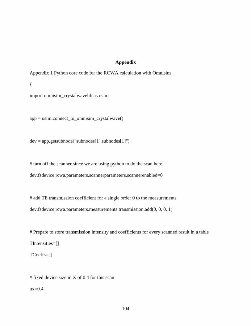
104
Appendix
Appendix 1 Python core code for the RCWA calculation with Omnisim
{
import omnisim_crystalwavelib as osim
app = osim.connect_to_omnisim_crystalwave()
dev = app.getsubnode("subnodes[1].subnodes[1]")
# turn off the scanner since we are using python to do the scan here
dev.fsdevice.rcwa.parameters.scannerparameters.scannerenabled=0
# add TE transmission coefficient for a single order 0 to the measurements
dev.fsdevice.rcwa.parameters.measurements.transmission.add(0, 0, 0, 1)
# Prepare to store transmission intensity and coefficients for every scanned result in a table
TIntensities=[]
TCoeffs=[]
# fixed device size in X of 0.4 for this scan
ux=0.4

105
for iz in range (0,10,1):
# scan device size in Z from 0.4 to 0.5 in step of 0.01
uz = 0.4 + iz*0.01
dev.fsdevice.setsize(uz,ux)
intens=[]
coeffs=[]
for isz in range (0,10,1):
# scan over mask size in Z as a fraction of device size in Z from 0.1 to 0.2 in step of 0.01
sz = 0.1 + isz*0.01
dev.fsdevice.objects[1].sizez = uz*sz
dev.fsdevice.rcwa.calculate()
dev.fsdevice.rcwa.preparemeasurementresults()
# get transmission intensity
inten = dev.fsdevice.rcwa.parameters.measurements.transmission.get(0, 0, 0, 0, 1)
intens.append(inten.real)
coeff = dev.fsdevice.rcwa.parameters.measurements.transmission.get(0, 0, 0, 1)
coeffs.append(coeff)
TIntensities.append(tuple(intens))
TCoeffs.append(tuple(coeffs))
# print out the results here, you can do whatever you want with them
# each row is for each fixed value of uz while changing the fraction of the mask in Z

106
# for instance, copy them to Excel for plotting
print TIntensities
print TCoeffs
osim.disconnect_omnisim_crystalwave()
}