Embed Size (px)
Citation preview

IEEE PEDS 2005
Design ofPower Stage and Controller for DC-DCConverter Systems Using PSPICE
N. D. Muhamad, M. R -Sahid, A. H. M. Yatim, N. R. N. Idris, and M. S. AyobPower Electronic Research Group (PERG)
Faculty ofElectrical EngineeringUniversiti Teknologi Malaysia81310 UTM Skudai, Johor
Abstract-A complete set of SPICE-compatible design equations In this paper we demonstrate that PSPICE alone can befor design buck converter system is developed in this paper. In used to design DC-DC converter systems. The designthis approach, the power stage and controller design equations equations can be programmed in compact form in PSPICE. Forare programmed in PSPICE. For this purpose, an option this purpose, an option available in PSPICE called Analogavailable in PSPICE called Analog Behavioral Modeling (ABM) Behavioral Modeling (ABM) is used. Both steady-state andis used. In this manner, the parameter of power stage and the dynamic design equations are programmed. A set of designcomponent values of the error amplifier can be easily obtained by equations is made as a subcircuit model and stored inmeans of PSPICE bias point analysis. The obtained parameters PSPICE's library. In this manner, the subcircuit of designcan be passed to other circuit models to perform frequency equations can be teated as a library component, maldng it easyresponse and transient analysis. The methodology of to use. The presence of this type of subcircuit in PSPICEdevelopment is presented in details. A design example is included makes a new approach to using PSPICE simulator in process ofto demonstrate the effectiveness of the proposed approach in design. This approach includes both design as well asdesigning DC-DC converter systems. simulation tools thus making extensive use of PSPICE in DC-
Keywords-DC-DC Converter, Computer-aided design, PSPICE, DC converter design cycle. Moreover, both the flexibility andControl loop design, Small-signal model capability of PSPICE as a stand-alone program can be
enhanced. This approach will facilitate the design of DC-DCI. INTRODUCTION converter systems in PSPICE and it will make the design more
convenient and efficient.In designing DC-DC converter systems, there are two
requirements to be satisfied: steady-state and dynamics. The Throughout this paper, a buck converter with voltage modesteady-state requirements can be satisfied by properly choosing control is used as an example to develop and verifl the designthe parameters of the power stage. The dynamic requirements procedure. The general procedure, however, can still be readilycan be met by using an appropriate controller. There are a extended to include other converters with different controlnumber of well-documented techniques and guidelines schemes provided that their transfer functions and designavailable for designing DC-DC converter systems [1-6]. equations are available.Today, most DC-DC converter system design is carried outwith the aid of a computer-aided circuit analysis program such II. DESIGN PROCESSas PSPICE. There are many SPICE-based models developed The buck converter with voltage mode control is shown infor simulating DC-DC converters, In general, three types of Fig. 1. This converter is used to illustrate the design processmodel can be identified: the detailed model, the large-signal and demonstrate its feasibility for DC-DC converters design.averaged model, and the small-signal model. All three models The converter system comprises the power stage, theare useful in analysis and design of DC-DC converter systems. compensator and the pulsewidth modulator (PWM). TheThe small-signal model is required to design the control system converter is assumed to be in continuous conduction modeof a DC-DC converter. However, the use ofPSPICE is limited (CCM) of operation.to validation of circuit designs. A DC-DC converter designusually needs some theoretical analysis and calculation. Thismakes calculation software, such as Mathcad, often used along A. iPowerSage,P mol and Contrerwith PSPICE in the process of design. The use of software in Using te averaging and linearization techniques, theaddition to PSPICE causes the process of design to be control-to-output transfer fimction of the buck convertersomewhat inconvenient and inefficient, including PWM, canl be obtained as
O-7803-9296-5/05/$20.00 © 2005 IEEE 903

(s A where V., fr, R, and D are the output voltage, switching1+ frequency, load resistance and steady state duty ratio
z (ES1) respectively.vc s+ s + s 2) Capacitance C is determined from maximum allowableQ-0 o2 peak-to-peak output ripple voltage Vpp = Av0 considerations:
where AVC < AvC C + Avc,ESR
Vg 1 1 R where Avc0, is the AC component of the voltage across the==-,DO = ,)zESR = , and Q = REsR and AVC,ESR is the AC component voltage across the filter
VP 7 RESRC w0L capacitance, C. However, it is known that the peak-to-peakripple voltage is independent of the voltage across the filtercapacitance [7] and is determined only by the ripple voltage of
Power Stage Rl L the RESR if
Vg- C> C,r,,I, = maX,{Rfmln, RfC (3)
_C3 Compensator 3) The peak-to-peak voltage ripple, Av0, is usually givenas a percentage ofthe output voltage, typically equal to or less
R2 C2 RI C1 than 1%. Ifthe condition described by (3) is satisfied, RESR for4--wV-[ -AW----~ ~- the prespecified peak-to-peak voltage ripple is
+
R3 REs~~~R < Av0f~L (4)
Vp Vref
III. COMPENSATOR DESIGN EQUATIONSThe loop shaping approach is simple and effective for
Figure 1. Buck converter with voltage mode control dealing with the plants having complex dynamic behavior.Among popular loop shaping method in power electronic
For the circuit in Figure 1 the power stage has the following applications is K-factor approach, introduced in [4]. The mainparameters: Vg= 12V, Vo= 5V, R= 1.25 Q, Rl = 50mQ. The feature of K-factor approach is that the circuit componentpower stage design parameters are inductance Lf, capacitance, values can be obtained without trial-and-error. This is one ofCf and ESR of capacitor, RESR. The peak value ofPWM, Vp, is the reasons why the K-factor approach is widely accepted byassumed to be 3 V. The compensator network consists of RI, many researchers [9-12]. Since the analysis ofthe control loopR2, R3, Rbias, Cl, C2, C3 and Vref. We assume that the value design equations using K-factor approach in PSPICE has beenof Vref is 2. 5V, Rb,. is 10 kQ and the rest are design published earlier [6] we repeat here, for the sake of brevity,parameters. only the essential.
The type-3 error amplifier is commonly used forB oer StageuDesigfLC,andREqtsRdetermine CCM of operation
compensation of buck, boost and buck-boost circuits due to itsThe values ofL, C, and RESR determine CCM of operation ability to provide the phase boost, Xboost:
and a prespecified peak-to-peak output voltage ripple. For agiven switching frequency, power stage components L, C, andRESR may be selected to meet the following criteria: ° <.boosI < 1800 (5)
1) The value of inductance is chosen to assure CCM. Tomaintain CCM down to one-fifth output current Jo, the The transfer fbnction ofthe type-3 error amplifier is givenminimum value for L is by
L 2.5(Vg- VO)D (2)n VO
JS R
904

w'Vk~~ 02.)i OCO (13)ACOK
-s+O
G~~(s) ~ 2 (6) It2is imporan Popitout tha ths deign procdue is{ S +11 general in the sense that it can be used to any suitable
'Jkiroco applications. For a specific application, this design proceduremust be suited to the requirements of those applications. In the
where qo. is the desired crossover frequency, K is the pole case of buck converter, an important constraint is that thefrequency and zero frequency control factor. The value of K crossover frequency must be less than one-fourth of thecan be adjusted depending on the phase boost (0,. required switching frequency. This constraint is required to avoid theto make the phase compensation. To use the K-factor approach, large signal instability [1]. The design of compensator followsthe crossover frequency, f,,, must be chosen, and then the gain, the design of power stage because power stage parameters,A,, and the phase, 4,, of power stage at cq must be found. In such as filter inductance, capacitance, and ESR of capacitance,short the computation procedures of K-factor approach are as are needed. The next step is to convert the obtained values offollows: poles and zeros to the component values of compensator. This
is a straightforward process. In short, the conversions occur as1) Calculate the gain, Aco and the phase, 46, of power follows:
stage at cw.:
G~~0l+I'~02 (w, f,12) (14)v Co~~Y'zesr)
A 0~ (7)
WO)JL QCe)I C2 =C3jjjl -1)15
WCO R (16)
=c ftn- (o~ tan 1 Qo (8)
R 3 ~~~~~~(17)
2) By knowing A.,., and ~ and specifying the phasemargin, PM, the phase boost required can be calculated as C§::
O'boost = PM 900 - o (9)
3) Then, K-factor is calculated as 2C1= l21
K =tan2 4os +450J (10) =Vref
J3(9
4) 'The two poles of the compensator are located at 0 e
Cco () IV. PSPICE IMPLEMENTATION1K ~~~~~~~~ThePSPICE simulator is provided with an extension called
Analog Behavioral Modeling (ABM). With ABM the simulator5) The two zeros of the compensator are located at can be used like a programming language and to solve general
mathematical problems by translating them to an electricaloiJ-oic. (12) ~~~~circuit. ABM in PSPICE is able to evaluate expressions that are
'z12 = 1) functions of circuit variables (voltages, currents, and simulationtie)usn the cotrlld uren an vltg so rces (G-and E

transcendent and ordinary, differential equations in theirimplicit or explicit form. In each case, the equations areconverted into electrical circuits and solved by PSPICE with a w - _DC analysis for only algebraic equations or a transient analysisfor systems of algebraic and differential equations. Editing the w w -linput file of PSPICE is relatively more comfortable than C3
programming in MATLAB, C or other programnning E Llanguages.
To implement the equations in PSPICE, all variables arecoded into voltages. The relevant equations are represented bydependent sources that are function of the coded variables and Figure 2. The result of design parameters using PSPICE bias point analysisconstants. There are two parts of design equations to beprogrammed in PSPICE: power stage and control loop. The Using averaged circuit model, frequency response of loop-power stage design equations to be programmed are equations gain based on the averaged circuit model was simulated by(2)-(4), while the control loop design equations are equations PSPICE AC analysis. The result is shown in Fig. 3. From the(7)-(19). All the equations are implemented in PSPICE by bode plot, we can see that the crossover phase is -119.60,using the .PARAM statement. By using the .PARAM statement indicating stable operation with PM of 60.40. The crossoverwe can create parameters and assign algebraic mathematical frequency is at 16.623 kHz. The differences between theexpressions to it. To enable the related parameters available in desired values (PM = 60.00 and f= 16.667kHz) and theschematic, ABM parts are used. The complete PSPICE listing results ofPSPICE are fairly small.of design equations is given in Appendix.
V. DESIGN EXAMPLE
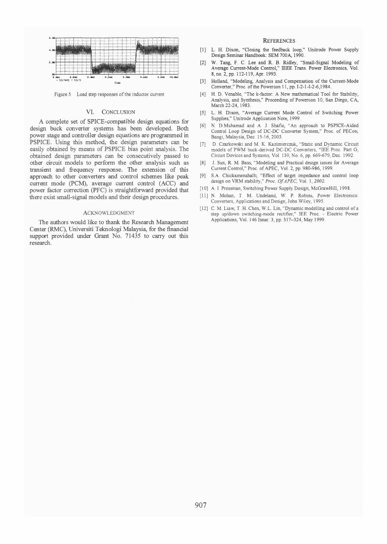
A design example is used to demonstrate the effectivenessofthe proposed approach in designing DC-DC converters. The ____ __,_____I _ _4_ _-_-_--j_____example is a buck converter operated in continuous conduction ............ .:. : ::mode (CCM) with the switching frequency,f, =100 kHz. The .only known parameters are: input voltage Vg = 12V, outputvoltage, VO = 5V, sawtooth peak voltage of PWM, Vp = 3V, Figure 3. Bode plot ofloop-gain (gain in dB and phase in degree)reference voltage, V,,f = 2.5V. The value of Rbi, is chosenarbitrarily as 10 k. For the control loop design, the crossover Transient analysis of the output voltage and the inductorfrequency, fi, is chosen asfJ/6 and the phase margin is chosen current based on the averaged circuit and switching detailedas 60°. This is a typical specification to design the compensator models are shown in Fig. 4 and 5, respectively. Both the resultsof a buck converter. ofthe averaged and switching detailed mbdel are superimposed
in the same graphs for comparison. It can be seen that, both theAll the given parameters above serve as inputs to the waveforms agree very well. To evaluate the performance of the
programmed design equations. It outputs the following system, load steps were performed. The load steps wereparameters: L, C, RESp, Cl, C2, C3, Rl, R2, and R3. Since programmed to step-down at 9.0 ms (from 4A to IA) and toPSPICE simulator always performs bias point analysis before step-up at 9.5 ms (from IA to 4A). It can be seen that the stepperforming other analysis, these values can be passed to other responses of the inductor current and the output voltage reflectcircuit models in order to perform the other analysis such as the behavior of a system with phase margin of about 60°,transient and frequency response. By doing so, the design verifying the design.phase and the verification phase appear to be simultaneouslyperformed by PSPICE. Obviously, this is one ofthe advantagesto program the design equations in PSPICE.
In this design example, the design parameters were passed ....
to the averaged circuit models to perform frequency response - r
and transient analysis. The design parameters were also passed ^...to the switching detailed model to perform transient analysis *S; . . - - . ., .} . . i5 1U.(cycle-by-cycle simulation). The result of design parameters UOUO . 8O05_ U)obtained by bias point analysis ofPSPICE is shown in Fig. 2. Itcan be seen from the result that all the obtained parameters Figure 4. Load step responses of the output voltagewere given in volt due to all the variables were already codedinto voltages. In order to make the design equations easy to use, it was
made as a subcircuit model and stored in PSPICE's library. Inthis manner, the design equations are treated as a librarycomponent.
906
1k ~--- REFERENCES
~~ I ~~Ii- - .f-~~~~~ ~ [1] L. H. Dixon, "Closing the feedback loop," Unitrode Power Supply--,-- .......i-
-.-- -.-4-. [2] Design Seminar Handbook: SEM 700A, 1990... 6 ,.;. ,.,:,.,.4,, ,.:..._,.:..W. Tang, F. C. Lee and R. B. Rid4ey, 'Small-Signal Modeling ofII ~~~~~~~~AverageCurrent-Mode Control," IEEE Trans. Power Electronics, Vol.
8, no. 2, pp. 112-119, Apr. 1993..I{LwI(LI) TL_ [3] Holland, "Modeling, Analysis and Compensation of the Current-Mode
Converter," Proc. ofthe Powercon 11, pp. 1-2-1-1-2-6,1984.Figure 5. Load step responses ofthe inductor current [4] H. D. Venable, "The k-factor: A New mathematical Tool for Stability,
Analysis, and Synthesis," Proceeding of Powercon 10, San Diego, CA,March 22-24,1983.
VI. CONCLUSION [5] L. H. Dixon, "Average Current Mode Control of Switching Power
A complete set of SPICE-compatible design equations for Supplies," Unitrode Application Note, 1999.designbuck convetr systemns has been developed. Both [6] N. D.Muhamad and A. J. Shafie, "An approach to PSPICE-Aideddesign buck converter systeTns has been aevelopea. tsotn Control Loop Design of DC-DC Converter System," Proc. of PECon,
power stage and controller design equations are programmed in Bangi, Malaysia, Dec. 15-16, 2003.PSPICE. Using this method, the design parameters can be [7] D. Czarkowski and M. K. Kazimierczuk, "Static and Dynamic Circuiteasily obtained by means of PSPICE bias point analysis. The models of PWM buck-derived DC-DC Converters, "IEE Proc. Part G,obtained design parameters can be consecutively passed to Circuit Devices and Systems, Vol. 139, No. 6, pp. 669-679, Dec. 1992.other circuit models to perform the other analysis such as [8] J. Sun, R. M. Bass, "Modeling and Practical design issues for Averagetransient and frequency response. The extension of this Current Control," Proc. ofAPEC, Vol. 2, pp. 980-986, 1999.approach to other converters and control schemes like peak [9] S.A. Chickamenahalli, "Effect of target impedance and control loopcurrent mode (PCM), average current control (ACC) and design on VRM stability," Proc. OfAPEC, Vol. 1,2002.power factor correction (PFC) is straightforward provided that [10] A. I. Pressman, Switching Power Supply Design, McGrawHill, 1998.there exist small-signal models and their design procedures. [11] N. Mohan, T M. Undeland, W. P. Robins, Power Electronics:
Converters, Applications and Design, John Wiley, 1995.[12] C. M. Liaw, T. H. Chen, W.L. Lin, "Dynamic modelling and control ofa
ACKNOWLEDGMENT step up/down switching-mode rectifier," IEE Proc. - Electric Power
The authors would like to thank the Research Management Applications, Vol. 146 Issue: 3, pp. 317-324, May 1999.Center (RMC), Universiti Teknologi Malaysia, for the financialsupport provided under Grant No. 71435 to carry out thisresearch.
907

APPENDIX
PSPICE Listing for Power Stage and Control Loop Design Equations
Power Stage and Control Loop Design EquationsPARAMETERS: PARAMETERS:pi = 3.14159265 w = (2*pirf
Mag_Buck ZESR = {SQRT((1 +(w*w)/(wzesr*wzesr)))}PARAMETERS: wzesr = {1/(Resr*C)}L = {1 .1*Lmin} Ph Buck_Zesr ={atan(w/wzesr)*1 80/pi}Resr = {lF(O.9*Rc>40m,40m,0.9*Rc)) wco = {2*pifco}C = (1.1*Cmin) PARAMETERS:R3 = 10k Mag_Buck LC = {(Vg/p)/SQRT(((w/(Q*w))*(w/(Q*w)))+(l-(w*w/(wo*wo)))*(1-(w*w/(wo*wo))))}Vp = 3 Ph Buck LC raw = {-atan((w/(Q*wo))I(1-(ww)/(wo*wo)))*180Wpi)Vref = 2.5V Ph_Buck-LC- {tF((14((w*w)(wo*wo)))<O,Ph_Buck_LC_raw-1 0,Ph_Buck_LC_raw)}f = {fco} Q = {RI(wo*L)}fs = 100k wo = {1/SQRT(L*C)}fco = 16.666kPARAMETERS: PARAMETERS:wi = {w/(Aco*k)) PowerStage = 'Mag-BuckLC*Mag_BuckkZesr}wp1 2 = {w/sqrt(k)} PARAMETERJ- - M-wzl 2 = {wlsqrt(k)} PHlPowerStage = tiPh Buck-Zesr+Ph_Buck_LC)PARAMETERS: PARAMETERS:Vg = 12 Mag_Buck_LCQatjfco = {(VgNp)/SQRT(((wco/(Q*Wco))*(wco/(Q*wco)))+(1-(wco*wco/(wo*wo)))*(1-(wco*wco/(wo*wo))))}Vo = 5 Mag Buck Zesr at fco = {SQRT((1 +(wco'wco)/(wzesr*wzesr)))}R = 1.25 Mag§Buck-fco :-{M-ag_Buck_LC_at fco*Mag_Buck Zesr_at_tco}PARAMETERS: PARAMETERS: PARAMETERS: PARAMETERS:PM =60 Lmin ={5*(Vg-Vo)*D/((PIU10)*fs*Vo/R)) Cmin = {max((1-D)/(2*Rc*fs),DI(2*Rc*fs))} Vr = (PVC*Vo/100}Aco = {PowerStage} D =(VoN{ } Rc = {fs*Lmin*Vr/(Vo*(1-D))} PVC = 1Pco = {Ph_PowerStage} PIL = 20k= {(Tan(((Pboost/4)+45)*pi/180))*(Tan(((PboosV4)+45)*pi/180))} PIL: Percentage of Inductor CurrentPboost = {PM-90-Pco} PVC: Percentage of Capacitor Voltage
908