Embed Size (px)
Citation preview

2614 IEEE TRANSACTIONS ON INDUSTRIAL ELECTRONICS, VOL. 60, NO. 7, JULY 2013
Design-Oriented Analysis and PerformanceEvaluation of a Low-Cost High-Brightness LEDDriver Based on Flyback Power Factor CorrectorDiego G. Lamar, Member, IEEE, Manuel Arias, Member, IEEE, Alberto Rodríguez, Student Member, IEEE,
Arturo Fernández, Member, IEEE, Marta M. Hernando, Senior Member, IEEE, andJavier Sebastián, Senior Member, IEEE
Abstract—This paper presents a new control strategy for powerfactor correctors (PFCs) used to drive high-brightness light-emitting diodes (HB-LEDs). This control strategy is extremelysimple and is based on the use of standard peak-current-modeintegrated controllers (PCMICs), reducing its cost and complexityin comparison to traditional PFC controllers. In fact, this methodis an alternative implementation of the one-cycle control to PFCsbelonging to the flyback family of converters, without introducinghigh complexity for reducing the total harmonic distortion. In thiscase, the use of a simple exponential compensation ramp instead ofa linear one is the proposed solution for drawing a sinusoidal inputcurrent. Moreover, the line current is cycle-by-cycle controlled,and therefore, the input-current feedback loop is extremely fast,which allows the use of this type of control with high-frequencylines. The proposed idea is to apply this simple control to aone-stage PFC in order to design a low-cost ac–dc HB-LED driver.However, the application of this control strategy to PFC belong-ing to the flyback family of converters is not obvious. Design-oriented considerations about its implementation in PCMIC willbe provided. Finally, an experimental prototype of this driver wasdeveloped.
Index Terms—AC–DC power conversion, current control, har-monic distortion, light-emitting diodes, power factor (PF), recti-fiers, switched-mode power supplies.
I. INTRODUCTION
IN THE LAST years, solid-state lighting technologyprogress has changed traditional solutions in lighting.
Nowadays, high-brightness light-emitting diodes (HB-LEDs)are very attractive light sources due to their excellent charac-teristics: high efficiency, high longevity, and low-maintenancerequirements [1], [2]. Also, HB-LED packages are more and
Manuscript received December 5, 2011; revised March 9, 2012; acceptedApril 15, 2012. Date of publication April 30, 2012; Date of current versionFebruary 28, 2013. This work was supported by the Spanish Ministry ofEducation and Science under Consolider Project RUE CSD2009-00046, ProjectDPI2010-21110-C02-0, Grant AP-2008-03380, and European Regional Devel-opment Fund grants.
D. G. Lamar, M. Arias, A. Rodríguez, M. M. Hernando, and J. Sebastiánare with the Grupo de Sistemas Electrónicos de Alimentación, Universidad deOviedo, 33204 Gijón, Spain (e-mail: [email protected]; [email protected]; [email protected]; [email protected]; [email protected]).
A. Fernández is with the European Space Agency, 22201 AZ Noordwijk,The Netherlands (e-mail: [email protected]).
Color versions of one or more of the figures in this paper are available onlineat http://ieeexplore.ieee.org.
Digital Object Identifier 10.1109/TIE.2012.2196905
more robust, introducing higher reliability than traditional lightsources (fluorescent lamps, incandescent lamps, etc.). SinceHB-LEDs are diodes, the default method for driving them iscontrolling the dc forward current through the semiconductor.If the primary energy source is the ac line, then some typeof ac–dc converter must be placed between the line and theHB-LEDs [3]–[6]. It is known that, if the total power handledby these converters is higher than 25 W, then the low-frequencyharmonic content of the line current must comply with specificregulations. For lighting equipment, the most widely used stan-dards are EN 61000-3-2, Class C [7], [8] and ENERGY STARprogram [9]. These regulations establish a very strict harmoniccontent, such that only very sinusoidal line waveforms are ableto comply with the aforementioned regulations. Therefore, theonly practical method to comply with these regulations is to useactive high-power-factor (PF) converters, commonly called PFcorrectors (PFCs).
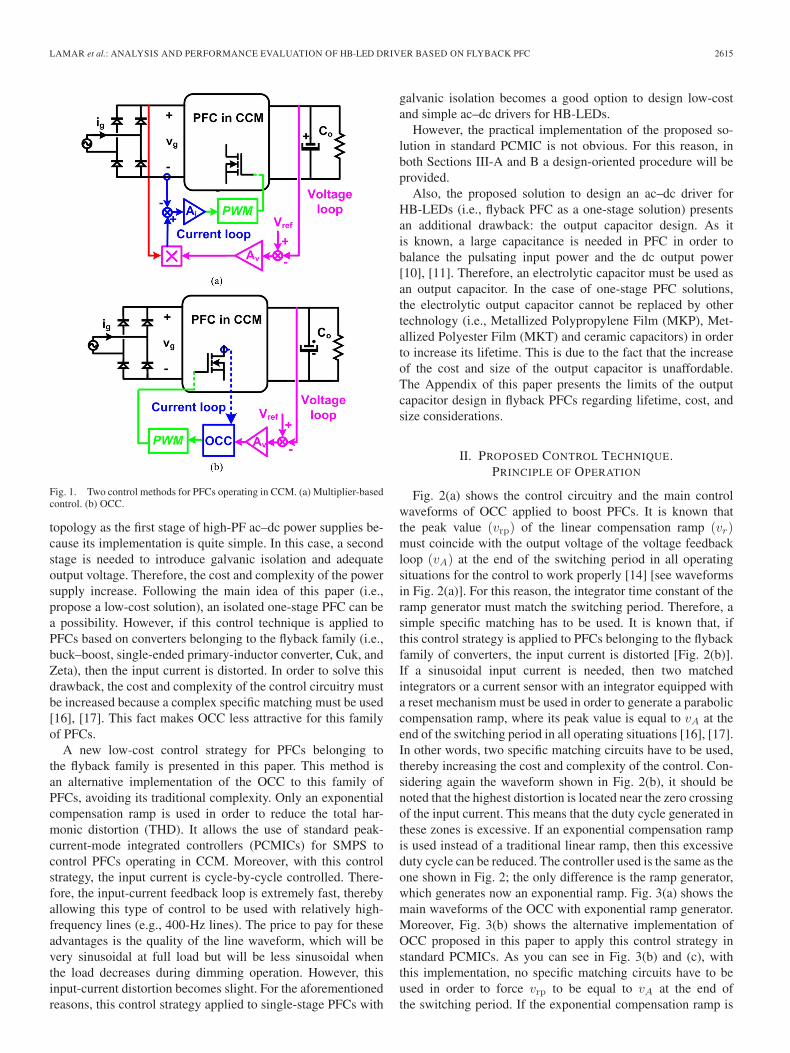
The classical control method of PFCs operating in con-tinuous conduction mode (CCM) for obtaining a perfectlysinusoidal line waveform is based on two feedback loops (aninput-current feedback loop and an output-voltage feedbackloop) and a multiplier [Fig. 1(a)] [10], [11]. However, the maindisadvantage of this option is the complexity of the controlcircuitry and its cost. Several controllers can be used for thispurpose, but they are not cheap, particularly in comparisonwith standard controllers for switching-mode power supplies(SMPSs). If the converter has to be a very low-cost one, theuse of PFC controllers based on a multiplier becomes relativelyexpensive.
With HB-LEDs being increasingly used in low-cost lightingapplications, the necessity for ac–dc drivers with optimizedcontrol circuitry that reduces their cost becomes more impor-tant. In the last years, a number of authors have proposeddifferent low-cost control strategies for PFCs operating in CCMand wide input-voltage range [12]–[17]. The goal of thesecontrol strategies is to simplify the existing control circuitrybased on a multiplier. The most significant one is the one-cyclecontrol (OCC) technique [Fig. 1(b)] [14]–[17]. It is importantto say that the OCC has not only been used in ac–dc convert-ers. The significance of the OCC has been extended to otherconverters, e.g., three-phase rectifier [18], [19], inverters [20],and bidirectional converters [21], due to its simplicity. In ac–dcconversion, this low-cost control technique is focused on boost
0278-0046/$31.00 © 2012 IEEE
LAMAR et al.: ANALYSIS AND PERFORMANCE EVALUATION OF HB-LED DRIVER BASED ON FLYBACK PFC 2615
Fig. 1. Two control methods for PFCs operating in CCM. (a) Multiplier-basedcontrol. (b) OCC.
topology as the first stage of high-PF ac–dc power supplies be-cause its implementation is quite simple. In this case, a secondstage is needed to introduce galvanic isolation and adequateoutput voltage. Therefore, the cost and complexity of the powersupply increase. Following the main idea of this paper (i.e.,propose a low-cost solution), an isolated one-stage PFC can bea possibility. However, if this control technique is applied toPFCs based on converters belonging to the flyback family (i.e.,buck–boost, single-ended primary-inductor converter, Cuk, andZeta), then the input current is distorted. In order to solve thisdrawback, the cost and complexity of the control circuitry mustbe increased because a complex specific matching must be used[16], [17]. This fact makes OCC less attractive for this familyof PFCs.
A new low-cost control strategy for PFCs belonging tothe flyback family is presented in this paper. This method isan alternative implementation of the OCC to this family ofPFCs, avoiding its traditional complexity. Only an exponentialcompensation ramp is used in order to reduce the total har-monic distortion (THD). It allows the use of standard peak-current-mode integrated controllers (PCMICs) for SMPS tocontrol PFCs operating in CCM. Moreover, with this controlstrategy, the input current is cycle-by-cycle controlled. There-fore, the input-current feedback loop is extremely fast, therebyallowing this type of control to be used with relatively high-frequency lines (e.g., 400-Hz lines). The price to pay for theseadvantages is the quality of the line waveform, which will bevery sinusoidal at full load but will be less sinusoidal whenthe load decreases during dimming operation. However, thisinput-current distortion becomes slight. For the aforementionedreasons, this control strategy applied to single-stage PFCs with
galvanic isolation becomes a good option to design low-costand simple ac–dc drivers for HB-LEDs.
However, the practical implementation of the proposed so-lution in standard PCMIC is not obvious. For this reason, inboth Sections III-A and B a design-oriented procedure will beprovided.
Also, the proposed solution to design an ac–dc driver forHB-LEDs (i.e., flyback PFC as a one-stage solution) presentsan additional drawback: the output capacitor design. As itis known, a large capacitance is needed in PFC in order tobalance the pulsating input power and the dc output power[10], [11]. Therefore, an electrolytic capacitor must be used asan output capacitor. In the case of one-stage PFC solutions,the electrolytic output capacitor cannot be replaced by othertechnology (i.e., Metallized Polypropylene Film (MKP), Met-allized Polyester Film (MKT) and ceramic capacitors) in orderto increase its lifetime. This is due to the fact that the increaseof the cost and size of the output capacitor is unaffordable.The Appendix of this paper presents the limits of the outputcapacitor design in flyback PFCs regarding lifetime, cost, andsize considerations.
II. PROPOSED CONTROL TECHNIQUE.PRINCIPLE OF OPERATION
Fig. 2(a) shows the control circuitry and the main controlwaveforms of OCC applied to boost PFCs. It is known thatthe peak value (vrp) of the linear compensation ramp (vr)must coincide with the output voltage of the voltage feedbackloop (vA) at the end of the switching period in all operatingsituations for the control to work properly [14] [see waveformsin Fig. 2(a)]. For this reason, the integrator time constant of theramp generator must match the switching period. Therefore, asimple specific matching has to be used. It is known that, ifthis control strategy is applied to PFCs belonging to the flybackfamily of converters, the input current is distorted [Fig. 2(b)].If a sinusoidal input current is needed, then two matchedintegrators or a current sensor with an integrator equipped witha reset mechanism must be used in order to generate a paraboliccompensation ramp, where its peak value is equal to vA at theend of the switching period in all operating situations [16], [17].In other words, two specific matching circuits have to be used,thereby increasing the cost and complexity of the control. Con-sidering again the waveform shown in Fig. 2(b), it should benoted that the highest distortion is located near the zero crossingof the input current. This means that the duty cycle generated inthese zones is excessive. If an exponential compensation rampis used instead of a traditional linear ramp, then this excessiveduty cycle can be reduced. The controller used is the same as theone shown in Fig. 2; the only difference is the ramp generator,which generates now an exponential ramp. Fig. 3(a) shows themain waveforms of the OCC with exponential ramp generator.Moreover, Fig. 3(b) shows the alternative implementation ofOCC proposed in this paper to apply this control strategy instandard PCMICs. As you can see in Fig. 3(b) and (c), withthis implementation, no specific matching circuits have to beused in order to force vrp to be equal to vA at the end ofthe switching period. If the exponential compensation ramp is

2616 IEEE TRANSACTIONS ON INDUSTRIAL ELECTRONICS, VOL. 60, NO. 7, JULY 2013
Fig. 2. (a) OCC with a linear ramp generator for a boost PFC. (b) OCC with a linear ramp generator for the flyback PFC.
Fig. 3. (a) Main waveforms of the control in Fig. 2(b) with an exponential ramp generator. (b) New implementation of OCC with an exponential compensationramp for the flyback family of PFCs. (c) Main control waveforms of new implementation of the OCC.
generated by vA using an RC circuit as a ramp generator, thenthe peak value of the compensation ramp is known and almostequal to the vA at the end of the switching period if the timeconstant defined by RC is high enough. In this case, the dutycycle is determined by the instant when vr + iSRS equals vA[Fig. 3(c)], which is equivalent condition to the OCC one shownin Fig. 3(a) (vr − vA equals iSRS) [14]. Also, Fig. 3(c) showsthe main control waveforms at full and low loads.
The expression of the exponential compensation ramp shownin Fig. 3(a) (magenta color) can be easily obtained
vr = vrp · e− t
τ − e−TSτ
1− e−TSτ
= vrp · e−− t
τ − e−μ
1− e−μ(1)
where vrp is the peak value of the exponential compensationramp (vr), τ is the time constant of the exponential compensa-tion ramp [Fig. 3(a) and (c)], TS is the switching period, and μis defined as
μ =TS
τ=
1
(τ · fS)(2)
where fS is the switching frequency.
The expression of the current through the magnetizing induc-tance of the flyback transformer at the end of the magnetizingperiod (i.e., iS2 in blue color in Fig. 3(a) at t = TSd) can becalculated when vr equals RSiS2
iS2 =vrpRS
· e−dμ − e−μ
1− e−μ(3)
where RS is the gain of the controlled switch current sensor andd is the duty cycle.
Applying Faraday’s law to the magnetizing inductance of theflyback transformer operating in CCM during the magnetizingperiod yields
vg = LfSiS2 − iS1
d(4)
where vg is the rectified input voltage (i.e., vg =VgP | sin(ωLt)|) and L is the magnetizing inductance ofthe flyback transformer. Analyzing also the demagnetizingperiod of the flyback, we obtain
Vo = nLfSiS2 − iS1
1− d(5)

LAMAR et al.: ANALYSIS AND PERFORMANCE EVALUATION OF HB-LED DRIVER BASED ON FLYBACK PFC 2617
where Vo is the output voltage and n is the turn ratio oftransformer of the flyback (i.e., n = n2/n1). By using (4) and(5), the expression of the duty cycle can be expressed as
d =Vo
Vo + VgP sin(ωLt) · n. (6)
Taking into account (3) and (4), the average input current isdefined as follows:
igav=(iS2+iS1)d
2=
(vrp(e
−dμ−e−μ)
RS(1−e−μ)− VgP sin(ωLt)d
2LfS
)d.
(7)
Three parameters will be defined in order to simplify thestudy of this static analysis
K =2LfSvrp(RSVgP )
(8)
M =Vo
nVgP(9)
in =Vo
Lfs(10)
where K is a dimensionless parameter used to study the bound-ary between CCM and discontinuous conduction mode (DCM),M is the conversion ratio at the peak of the line voltage (VgP ),and in is used in order to normalize significant currents of thisstatic study. From (6)–(10), we can normalize igav
igav = in
[e
− M
(M+sin(ωLt))μ
−e−μ
1−e−μ K − M ·sin(ωLt)(M+sin(ωLt))
]
2 (M + sin(ωLt)) · n. (11)
Using the same procedure used to calculate iavg [i.e., using(3), (4), (6), and (8)–(10)], we can normalize the expression ofthe current through L at the beginning of the switching period[i.e iS1 in blue color in Fig. 3(a)]
iS1 =in2
⎡⎢⎣e
− M
(M+sin(ωLt))μ
− e−μ
1− e−μK − 2M · sin(ωLt)
(M + sin(ωLt))
⎤⎥⎦ .
(12)
In the case of operating in DCM, (4) is also valid (with iS1 =0); however, (5) and (7) become
Vo =nLfSiS2
d′(13)
igav =iS2
2d (14)
where d′TS defines the demagnetizing period of L.The final expressions of igav and iS2 in DCM as a function of
the line angle (ωLt) may be deduced using the same procedureused in CCM but using (3), (4) with iS1 = 0, (8)–(10), (13)and (14). Thus, we obtain a transcendent equation that must benumerically solved.
Fig. 4. Normalized line current for different values of μ.
The limit between CCM and DCM can be calculated by set-ting iS1 = 0 (12). Therefore, the critical value of K that definesthe boundary between CCM and DCM can be calculated as
Kcrit(ωLt) =2M · sin(ωLt)
(M + sin(ωLt))
1− e−μ
e− M
(M+sin(ωLt))μ
− e−μ
. (15)
As (15) shows, Kcrit(ωLt) has different values, depend-ing on the line angle (ωLt). Hence, the maximum value ofKcrit(ωLt) is
Kcrit_max =2M(1− e−μ)
μe−μ (16)
and the minimum value of Kcrit(ωLt) is
Kcrit_min =2M
(M + 1)
1− e−μ
e− M
(M+1)μ
− e−−μ
. (17)
Finally, we define two dimensionless parameters
α =K
Kcrit_max=
Kμe−μ
2M(1− e−μ)(18)
αKmin =α(Kcrit_min) =Kcrit_min
Kcrit_max. (19)
The design parameter α defines three operating modes:If α > 1, PFC operates always in CCM (K > Kcrit_max); ifα < αKminK < Kcrit_min), it operates always in DCM; and if1 > α > αKmin, it operates in both modes (Kcrit_min < K <Kcrit_min).
At this point, the input current of the PFC can be represented.Fig. 4 shows the normalized input current for several valuesof μ for the same PFC design (M = 0.75 and α = 2). Asyou can see, when an exponential compensation ramp is used,there is an optimum value of μ that minimizes the THD ofthe line current (Fig. 4) for each design (α and M ) at nominalconditions (i.e., nominal input voltage and full load). When μis chosen (Fig. 4), the design parameter α must be calculatedgreater than unity in order to ensure CCM operation duringthe entire line angle at nominal conditions and therefore drawa very sinusoidal input current. Nevertheless, even if the PFCis designed to operate in CCM during the entire line angleat nominal conditions, it should be noted that it will pass

2618 IEEE TRANSACTIONS ON INDUSTRIAL ELECTRONICS, VOL. 60, NO. 7, JULY 2013
Fig. 5. Line current waveforms for different operation points, defined by Kvalue versus Kcrit, when the optimum value of the exponential ramp (μ =4.017) is selected for α = 1.5 and M = 1.5 design.
through different operating modes if the operating point of thePFC changes. If the PFC operates at undervoltage or heavy-load situations (i.e., α increases α > 1), it remains in CCMduring the entire line angle, drawing a very sinusoidal inputcurrent. However, if the load decreases or the input voltageincreases, α decreases. If α decreases to below unity (α < 1),then two operation modes are possible (see the waveformsshown in Fig. 5): CCM (solid line) and DCM (dotted line).Therefore, Fig. 5 could represent dimming operation of theac–dc HB-LED driver, where α = 1.5, 0.86, 0.54, and 0.22represent the operation points at Pmax, 0.5Pmax, 0.25Pmax,and 0.125Pmax, respectively. As you can see, the input currentis slightly distorted in these operation situations. However, itremains very sinusoidal, making the proposed control strategysuitable for dimming operation. In order to adequately checkthis slight distortion, Fig. 6 shows the PF and THD versus αdifferent PFC designs. Even if α decreases, the distortion of theinput current remains slight.
III. PRACTICAL CONSIDERATIONS FOR AC–DC HB-LEDDRIVER DESIGN BASED ON THE PROPOSED SOLUTION
As was aforementioned, a proper design of a PFC belongingto the flyback family of converters based on the proposed con-trol strategy should be an option to design an ac–dc HB-LEDdriver. In the following section, the practical considerations ofits design will be provided. The design considerations of theoutput capacitor are provided in the Appendix.
Fig. 6. (a) PF versus α for several flyback optimum PFC designs. (b) THDversus α for several flyback optimum PFC designs.
Fig. 7. (a) Values of μ to minimize the THD for different design conditions(M and α). (b) igpRS/Vgp value as a function of M and α.
A. Design Procedure
The design procedure of a PFC belonging to the flybackfamily of converters with the proposed control strategy is verysimple. The inputs of this design are the output voltage Vo, thepeak value of the input voltage Vgp, and the maximum outputpower Pmax.
First, M must be calculated from (9) choosing n according toa tradeoff between current and voltage stress in both the powertransistor and diode. As in any PFC belonging to the flybackfamily of converters, the voltage across the main switch mustbe bounded. This is the main restriction.
Second, α must be chosen. This value should be selectedgreater than one, which guarantees CCM for the entire line an-gle at nominal conditions. Once M and α are known, determinethe value of μ according to the plot given in Fig. 7(a), whichdefines the optimum values of μ for different PFC designs.As you can see, the μ factor is between three and six (whichmeans that τ is between three and six times the switchingperiod (TS)) in order to minimize THD of the input currentfor many standard designs.
Third, the quotient Vrp/RS must be calculated. For thispurpose, a perfect sinusoidal line waveform is assumed (igp =2Pmax/Vgp), which is a reasonable approach when the rightvalue of μ has been chosen. Thus, the value of igav at ωLt =π/2 and full load obtained from (11) must be equal to the valueof igp calculated from the power balance. From this equalityand taking into account (9) and (18), the value of the quotientVrp/RS can be easily calculated. To make this calculation eveneasier, a plot of igpRS/Vgp as a function of M and α is givenin Fig. 7(b). Once the value of Vrp/RS has been calculated, the

LAMAR et al.: ANALYSIS AND PERFORMANCE EVALUATION OF HB-LED DRIVER BASED ON FLYBACK PFC 2619
Fig. 8. Normalized line current waveforms for a universal input-voltagedesign (μ = 4.017, α = 1, and M = 1.5).
individual values of Vrp and RS can be chosen freely but takinginto account that they must be compatible with the controllervoltage levels.
Finally, we have to calculate the value of the PFC induc-tance L. Once the value of the quotient Vrp/RS is known, thevalue of L can be easily calculated from the definitions of K(8), Kcrit_max (16), and α (18).
As was mentioned in the previous section, the distortionof the input current is negligible for α values greater thanthe design value (Fig. 6). This conclusion is very importantand permits the use of this control strategy in the case ofPFCs working within the universal range of input voltages.In this case, the design criterion is very simple: The PFCmust be designed to have the desired high PF and low THDat the highest nominal input voltage, for example, M = 1.5,α = 1, and μ = 4.017 in Fig. 8. Note that the PF and THDwill have better values at the lowest input voltage because αincreases (Fig. 6).
As it is well known, the current control mode is unstable,operating in CCM when the duty cycle is greater than 0.5. Toavoid this problem, a compensation ramp is introduced. In thiscase, the slope of the compensation must be high enough toavoid instabilities. However, in DCM, the current is zero atthe beginning and end of each switching period. Therefore, thecurrent is reset at the beginning of the switching period, andno instabilities take place. In the proposed control strategy, theslope of the compensation ramp is constantly changing due tothe fact that an exponential ramp is used to reduce the THDof the input current. At this point, the stability of the proposedcontrol strategy must be checked when both d > 0.5 and theflyback PFC is operating in CCM. The stability condition iswell known applied to flyback
mc =∂vr∂t
∣∣∣∣t=dTS
> 0.5(m2 −m1) =0.5RS
L
(vg −
Vo
n
)(20)
where mc is the slope of the compensation ramp, m1 is theslope of the inductor current during the magnetizing period, andm2 is the slope of the inductor current during the demagnetizing
period. The stability condition can be normalized by using (6)and (8)–(9)
2Kμe− M
(M+sin(ωLt))μ
> (sin(ωLt)−M) (1− e−μ). (21)
Once (21) is calculated, the stability condition for eachflyback PFC design using the proposed control strategy canbe easily checked in CCM (i.e., K > Kcrit(ωt)) when d >0.5. Mathematical software has been used to check (21) forrealistic designs of flyback PFC (i.e., M = [0, 1.5], K =[Kcritmax, 4Kcritmax], and μ = [3, 6]). The results show that noinstabilities appear operating in CCM. Therefore, this controlstrategy is stable for any ac–dc HB-LED driver design.
Moreover, this concept can be easily explained that the valueof the compensation ramp slope will be always enough toavoid instabilities when the converter is operating in CCM.From Fig. 3(a), it can be easily deduced that the slope of theexponential compensation ramp is higher than m2 for a valueof the duty cycle in the middle range. When the duty cycle tendsto unity and the converter is still operating in CCM, then bothm1 and m2 tend to zero, whereas the slope of the compensationramp is never zero, due to the selected value of μ (in fact,this slope would be zero only if μ was the infinity). Therefore,instabilities never take place.
B. Implementation of the Proposed Control Strategy inStandard and Low-Cost PCMICs
Summarizing the considerations in Section II, this controlstrategy can be implemented by using only four blocks: anoscillator, an error amplifier (subtractor included), a pulsewidthmodulator, and a ramp generator with its reset. The three firstblocks are included in any standard [i.e., UC3824, Fig. 9(a)] orlow-cost [i.e., UC3843, Fig. 9(b)] PCMIC for SMPS. Moreover,the ramp generator with its reset can be easily built with afew discrete analog components. The values of the resistorsRramp and the capacitor Cramp have been chosen in orderto generate an adequate compensation ramp to minimize theTHD of the input current (i.e., defining the optimum μ value).This compensation ramp is an exponential waveform generatedby vA. Due to this fact, the asymptotic value of compensationramp is equal to vA, which makes very easy to obtain thedesired values of μ [typically in the range of three to six;see Fig. 7(a)]. Therefore, the specific matching circuit thatassures OCC operation is extremely simple in the proposedimplementation.
Due to fact of being an HB-LED driver, the dc outputcurrent (instead of the output voltage) is controlled by thefeedback loop [green circuitry in Fig. 9(a)]. A potentiometerPref is used to change the reference of the current regulator toperform analog dimming. Furthermore, resistors Ro1 and Ro2
and transistor Qo generate an adequate voltage to compensatethe chip comparator offset and the base–emitter voltage drop oftransistor which generates the compensation ramp (i.e., Qramp).Moreover, using a UC3824, the clock signal must be adapted inorder to reset the compensation ramp (Cr and Rr circuit). Thevalues of RD, RF1, RCL1, and RCL2 and the values of CF1,

2620 IEEE TRANSACTIONS ON INDUSTRIAL ELECTRONICS, VOL. 60, NO. 7, JULY 2013
Fig. 9. Two possible implementations of the proposed control strategy with commercial PCMIC. (a) UC3824. (b) UC3843.
CCL1, and CCL2 complete the output current feedback loop.Finally, a protection circuit (resistors Rp1 and Rp2) has beenimplemented to detect open circuit operation at the output dueto an HB-LED failure. It should be noted that this protectioncircuit is needed because the converter operates as a currentsource.
Another possibility is to use a standard PCMIC with aminimal external-part count (i.e., UC3843) in order to reduceto cost of the ac–dc HB-LED driver [Fig. 9(b)]. These kinds ofICs present some drawbacks to implement this control strategy:The pin for clock signal is not available, the reference of thevoltage regulator is a constant value, and the pin for circuitry

LAMAR et al.: ANALYSIS AND PERFORMANCE EVALUATION OF HB-LED DRIVER BASED ON FLYBACK PFC 2621
TABLE ILIST OF COMPONENTS OF THE EXPERIMENTAL PROTOTYPE
protection is not available. Therefore, dimming operation seemsnot to be possible. However, these drawbacks can be overcome[Fig. 9(b)]. The clock signal needed to reset the compensationramp can be obtained from a derivative circuit connected tothe output (Cr, Rr, and Dr). With resistors Rp1, Rp2, Rp3,and Rp4 and transistors Qp1 and Qp2, a protection circuit canbe built to detect open circuit operation at the output. Finally,the adder circuit implemented using the operational amplifierAOad allows a control of the output current level and, therefore,dimming operation.
IV. EXPERIMENTAL RESULTS
A prototype of a flyback PFC as an ac–dc HB-LED driverwas built and tested. It was controlled by the proposed controlstrategy which was implemented using a commercial PCMIC(UC3824). The circuit has been performed according to thescheme shown in Fig. 9(a), and the components are detailedin Table I. The converter output is connected to four stringsof four HB-LEDs LXK2PW14T00 (Luxeon). A simple resistor(0.33 Ω/6 W) has been used to equalize the current of eachstring [Fig. 9(a)]. This method of driving multiple strings ofHB-LEDs introduces additional power losses. In order to solvethis drawback, other equalization methods can be used decreas-ing power losses generated by the equalization circuit [22]. Itshould be noted that the converter has been designed for analogdimming which is simpler than other dimming techniques andtherefore the most adequate for low-cost applications [23].The main drawback is that the peak emission wavelength ofHB-LEDs tends to shift with the forward current, which canlead to color variations. However, this problem only imposessignificant challenge when the HB-LEDs are used for applica-tions where color stability is of primary concern (liquid crystaldisplay). The rated operating conditions of this converter are asfollows: vgRMS = 110 V, Io = 2−0.8 A, Pg = 30−10 W, andVo = 14−13 V.
The control circuitry has been designed to obtain a highPF value just when the converter stabilizes its temperature(HB-LEDs at room temperature). Fig. 10 shows the evolutionof the PF, the THD, and the HB-LED temperature (measuredon the heat sink at 3 mm from one HB-LED lead) duringthe warm-up process. As this figure shows, the final operationtemperature is reached after 70 min of operation. During thewarm-up process, the voltage across the HB-LEDs becomes
Fig. 10. Evolution of the PF, THD, and temperature during the warm-upprocess.
Fig. 11. (a) Line current at the end of the warm-up process. (b) Harmoniccontent of the ac–dc HB-LED driver prototype.
lower, and therefore, the power handled by the converter de-creases. Due to the very simple control circuitry proposed, theline current remains more or less constant during the warm-up process. This fact is reflected in the evolution of the PFand THD, which change from 0.998 and 5.1 (at the beginningof the warm-up process) to 0.996 and 7.8 (at the end ofthis process), respectively. Fig. 11(a) shows the line currentwaveform corresponding to the end of the warm-up process.The harmonic content at the end of the warm-up process isshown in Fig. 11(b), where it is compared with the limitsimposed by the EN 61000-3-2 regulation in Class C. As thisfigure shows, the prototype complies with the aforementionedregulations.
Fig. 12 shows the experimental waveforms of the line currentobtained in analog dimming operation when the currents acrosseach string are 0.4, 0.3, 0.2, and 0.1 A, corresponding to outputcurrents of 1.6, 1.2, 0.8, and 0.4 A. The dimming operation isperformed by changing the position of the potentiometer Pref .These figures show that the experimental PF (black color) isvery high in all operating conditions. Also, the experimentalresults have been compared with the theoretical ones (in red

2622 IEEE TRANSACTIONS ON INDUSTRIAL ELECTRONICS, VOL. 60, NO. 7, JULY 2013
Fig. 12. Line current during dimming operation.
color). As you can see, the theoretical waveforms match withthe experimental ones. Moreover, the PF and THD results, bothexperimental and theoretical, are very close.
Fig. 13 shows the output voltage and the current through theluminaire formed by four strings of HB-LEDs. As can be seen,a significant low-frequency ripple appears in the output current.As it is known, this is due to the energy transfer process of PFCsused as a one-stage PFC. The only way to reduce this ripple isto increase the output capacitance. Therefore, the electrolyticcapacitor cannot be removed, and the lifespan of the ac–dc HB-LED driver is reduced. However, this is the price to pay of usinga simple and low-cost solution for designing an ac–dc HB-LEDdriver.
Another interesting feature of the proposed control circuitryis its ability to operate with high-frequency lines (like the400-Hz line used in avionics). This is due to the fact thatthe peak-current-mode control provides cycle-by-cycle controlof the input current. The results obtained for different linefrequencies are given in Fig. 14.
V. CONCLUSION
A new method to control PFCs belonging to the flybackfamily of converters has been presented in this paper. The
Fig. 13. Output voltage and current through the HB-LEDs.
Fig. 14. Line current for different line frequencies.
method is based on the use of standard PCMICs withoutmultiplier. In fact, this method is an alternative implementationof the OCC to the PFCs belonging to the flyback family ofconverters. Only an exponential compensation ramp is used inorder to reduce THD. As a consequence of its simplicity, theinput current at different operation points to the nominal one isslightly distorted. Moreover, the input-current feedback loop isextremely fast, which allows us to use this type of control withrelatively high-frequency lines.
This control strategy applied to single-stage PFCs makessense in the case of relatively low-power and wide-input-voltage-range applications, such as ac–dc HB-LED drivers.However, the application of this control strategy to PFC belong-ing to the flyback family of converters is not obvious. Both thestatic analysis of this control strategy and the design-orientedconsiderations about its implementation in PCMIC have beenprovided. Finally, an experimental prototype has validated alltheoretical results presented in this paper.

LAMAR et al.: ANALYSIS AND PERFORMANCE EVALUATION OF HB-LED DRIVER BASED ON FLYBACK PFC 2623
APPENDIX
DESIGN CONSIDERATIONS OF THE OUTPUT CAPACITOR IN
CONVERTERS BELONGING TO THE FLYBACK
FAMILY OF PFCS
There are limits in the design of the output capacitor in PFCsbelonging to the flyback family of converters. It is known thatthe output capacitor of PFCs balances the pulsating input powerand the dc output power. A large capacitance is needed, andtherefore, an electrolytic capacitor is often used. This makes itquite bulky, and its size increases as either a low voltage level ora very low output voltage ripple is specified for a given power.Capacitor size is a further limitation for the use of a flybackPFC as a one-stage solution to design a complete ac–dc powersupply due to the fact that this capacitor is the output capacitorof the power supply [24], [25].
Also, the lifetime of the electrolytic capacitor is very limiteddue to its liquid electrolyte. This fact can be another obstacleto the design of an ac–dc power supply for long-lifetimeloads, for example, ac–dc HB-LED drivers. Some authors havepresented solutions to replace this electrolytic capacitor byother technology (i.e., MKT, MKP, and ceramic). However,these solutions are suitable for ac–dc power supplies based ontwo-stage structures [26], [27]. The first stage is a boost PFCthat draws a sinusoidal input current allowing relatively highlow-frequency output-voltage ripple. In this case, the outputcapacitance can be reduced, and a nonelectrolytic capacitoris used. The second stage both gives galvanic isolation andreduces the low-frequency output-voltage ripple to adequatethe output voltage to HB-LEDs. However, in the case of aflyback PFC, the electrolytic capacitor cannot be replaced byother technologies because the increase of the size and cost ofthe output capacitor becomes unaffordable. Therefore, the onlysolution is to increase the lifetime of the output electrolyticcapacitor. Next, we are going to evaluate the limits of thecommercial electrolytic capacitors.
Lifetime models of electrolytic capacitors are composed bysome datasheet parameters given by manufacturers and someoperation stresses defined by application as temperature, ripplecurrent, and applied voltage. The most common structure of alifetime model is the following [28]:
LX = L0 ·KT ·KR ·KV (A1)
where L0 is the nominal lifetime, KT is the temperature factor,KR is the current ripple factor, and KV is the voltage factor.
L0 is the lifetime of the electrolytic capacitor for givenambient temperature, ripple current, and voltage. These data aregiven by manufacturers in their datasheets. The typical nominallifetime of an electrolytic capacitor is 12 000 h at 85 ◦C.However, nowadays, manufacturers present long-lifetime ca-pacitors useful at 140 ◦C, which present L0 greater than15 000 h at 85 ◦C (e.g., B41692 and B41792 of EPCOS [29]).KT defines the effect of temperature in the lifetime of
electrolytic capacitors. The manufacturers establish the well-known Arrhenius law: A drop of the ambient temperature by10 ◦C doubles the lifetime
KT = 2T0−Ta
10 (A2)
Fig. 15. Parameterized lifetime diagrams for EPCOS series B41692 andB41792. (a) With derating voltage. (b) Without derating voltage.
where T0 is the rated temperature given by manufacturers in thedatasheets and Ta is the ambient temperature.
KR defines the impact of the applied ripple current on theself-heating of the electrolytic capacitor and, therefore, on itslifetime. KR depends on the ratio between the ripple current ofthe application (Ia) and the nominal ripple current establishedby manufacturers in datasheets (I0). Different manufacturersdefine different KR models in their products, but all of themcoincide in the same point: Operating ripple currents belowthe rated ripple current (i.e., Ia/I0 < 1) cause less temperaturestress in electrolytes. This fact may extend the lifetime of elec-trolytic capacitors (i.e., KR > 1). The frequency dependenceof the ripple current is taken into account by correction factorsgiven by manufacturers in their datasheets.KV estimates the influence of the applied voltage in the
lifetime of electrolytic capacitors. In fact, KV is a multiplierfor voltage derating. In other words, if the applied voltage (Va)is lower than the rated voltage specified by manufacturers indatasheets (V0), then the stress in the dielectric layer decreases.This fact makes less consumption in the electrolyte by self-heating, and therefore, the lifetime of the electrolytic capacitoris increased (i.e., KV > 1).
To provide the users of their products with some useful toolsfor the lifetime estimation of electrolytic capacitors, manufac-turers provide lifetime diagrams to simplify the calculation.These lifetime diagrams consider the aforementioned modeland show permissible combinations of model parameters (i.e.,T0, Ia/I0, and Va/V0) graphically. Fig. 15(a) and (b) showsthese lifetime diagrams. As you can see, lower values of Ia/I0,Va/V0, and T0 increase the lifetime of electrolytic capacitors.
Now, the idea is to investigate the increase of lifetime com-mercial capacitors by minimizing their stresses (i.e., decreasing

2624 IEEE TRANSACTIONS ON INDUSTRIAL ELECTRONICS, VOL. 60, NO. 7, JULY 2013
Fig. 16. Minimum volume of commercial capacitors versus the lifetime for some output power processed by the flyback PFC and some output voltages.
Ia/I0, Va/V0, and Ta and increasing KR, KV , and KT factors).In our study, T0 is constant and equal to 85 ◦C, which isthe ambient temperature specified in HB-LED applications.Decreasing Ia/I0 factor implies either to increase I0 or todecrease Ia by putting some capacitors in parallel. Both actionsimply a size increase in the electrolytic capacitor. Also, thesize of the electrolytic capacitor increases as either the appliedvoltage decreases (Va) for a given power or the rated voltageincreases. In other words, the size of the electrolytic capacitorincreases as the capacitor is maximized to derate its lifetime.
A commercial series of electrolytic capacitors was investi-gated: B41692 and B41792 of EPCOS [29]. Capacitor exploita-tion factor (EF) was considered in this study [24], [25]. Thisconcept is closely related to the fact that commercial capacitorshave capacitance values and rated voltage values that vary indiscrete steps. Therefore, the closer the design values to thecommercial values are, the lower the size of the storage capaci-tor is. For this reason, 25-, 40-, and 63-V electrolytic capacitorswere selected for output-voltage applications of 14, 28, and56 V, respectively (corresponding to strings of 4, 8, and16 HB-LEDs). A sinusoidal output-voltage ripple was consid-ered in order to simplify the study. Also, maximum 10% output-voltage ripple is defined. Furthermore, the output power rangedefined for this study is between 25 and 200 W.
Let us explain how the optimization process of minimizationof the commercial capacitor volume is. The output capacitanceof the flyback PFC is calculated for each output power, outputvoltage, output-voltage ripple, and lifetime. The maximumcapacitance and maximum diameter of the commercial elec-trolytic capacitor are selected for each rated voltage. First, thenumber of commercial capacitors necessary to obtain flybackPFC capacitance is calculated according to the EF. Then, thesecapacitors are tested against output current. If output current isgreater than the level specified by the commercial capacitors,then higher number of lower capacitors in parallel should beused. As a consequence, each single capacitor has smallercapacitance and diameter to comply with the output currentvalues.
Finally, Fig. 16 describes the minimum volume of com-mercial capacitors versus lifetime for different output voltages(solid lines). Each graph has been drawn for different outputpowers processed by the flyback PFC. The volume of theflyback PFC magnetic component is included in the plots
(dotted lines) as reference to compare the volume of the outputcapacitor for each particular power supply design. This willhelp to decide when the capacitor volume is excessively high.ETD cores were used for the magnetic component designs.Each magnetic component design depends on the choice ofthe boundary between the CCM and DCM: 33% of the powerprocessed in our case. All the capacitor designs are highlightedby points in each graph. As you can see, each design introducesan output-voltage ripple. In addition, the graphs in Fig. 11highlight a number of important conclusions.
1) The capacitor volume lines show that high lifetimecapacitor designs, in the range of 25–200-W outputpower, are possible at 85 ◦C for flyback PFCs: around200 000 h for 56-V output voltages and around400 000 h for both 28- and 14-V output voltages. Also,the volume of these designs is reasonable in comparisonto the magnetic component (dotted lines). The maindrawback of these designs is their cost because theselong useful life capacitor series are more expensive thantraditional electrolytic capacitors.
2) The lifetime of the output capacitor depends strongly onthe output voltage of the flyback PFC and does not dependon the output power. As you can see, the maximumlifetime achieved at 56-V output voltage is 250 000 h.However, the maximum lifetime achieved at either 28-or 14-V output voltage is 450 000 h. This is due to thefact that the output capacitors at low output voltage canbe highly derated. Therefore, lower Va/V0 factor canbe achieved introducing greater voltage multipliers inthe lifetime model (KV ). This concept can be easilyexplained in Fig. 15. The maximum lifetime achievedat 85 ◦C depends on the derating of the output voltage:450 000 h with output-voltage derating [Fig. 15(a)] and250 000 h without derating [Fig. 15(b)].
3) The capacitor volume lines show an asymptotic lifetimevalue not dependent on the output power: 250 000 h for56-V output voltage and 450 000 h for both 28- and14-V output voltages. This means that the output ca-pacitor of flyback PFC cannot be infinitely derated inorder to increase its lifetime (e.g., either using more smallcapacitors in parallel or using higher rated output-voltagecapacitors).

LAMAR et al.: ANALYSIS AND PERFORMANCE EVALUATION OF HB-LED DRIVER BASED ON FLYBACK PFC 2625
4) The asymptotic lines of capacitor volume versus the life-time show optimum designs at the zone of slope change.Each design in the diagram is defined by an output-voltage ripple. Therefore, an optimum lifetime design at56-V output voltage must be done with a specificationof the output-voltage ripple between 2% and 3%. In thecase of 14- and 28-V output voltages, the output-voltage-ripple specifications are between 4% and 5% and between3% and 4%, respectively. Also, the capacitor volume andthe magnetic volume are very close in the design zonesfor the 14- and 28-V output voltages. However, capacitorvolume is lower than the magnetic volume in the designzones for the 56-V output voltage.
REFERENCES
[1] I. L. Azevedo, M. G. Morgan, and F. Morgan, “The transition to solid-statelighting,” Proc. IEEE, vol. 97, no. 3, pp. 481–510, Mar. 2009.
[2] M. S. Shur and R. Zukauskas, “Solid-state lighting: Toward superiorillumination,” Proc. IEEE, vol. 93, no. 10, pp. 1691–1703, Oct. 2005.
[3] H.-J. Chiu, Y.-K. Lo, J.-T. Chen, S.-J. Cheng, C.-Y. Lin, and S.-C. Mou, “Ahigh-efficiency dimmable LED driver for low-power lighting application,”IEEE Trans. Ind. Electron., vol. 57, no. 2, pp. 735–743, Feb. 2010.
[4] D. G. Lamar, J. S. Zuniga, A. R. Alonso, M. R. Gonzalez, andM. M. H. Alvarez, “A very simple control strategy for power factorcorrectors driving high-brightness LEDs,” IEEE Trans. Power Electron.,vol. 24, no. 8, pp. 2032–2042, Aug. 2009.
[5] Y.-C. Li and C.-L. Chen, “A novel single-stage high-power-factor ac-to-dc LED driving circuit with leakage inductance energy recycling,” IEEETrans. Ind. Electron., vol. 59, no. 2, pp. 793–802, Feb. 2012.
[6] R. A. Pinto, M. R. Cosetin, A. Campos, M. A. Dalla Costa, and R. N. doPrado, “Compact emergency lamp using power LEDs,” IEEE Trans. Ind.Electron., vol. 59, no. 4, pp. 1728–1738, Apr. 2012.
[7] Electromagnetic Compatibility (EMC)—Part 3: Limits–Section 2: Limitsfor Harmonic Current Emissions (Equipment Input Current < 16 A perPhase), 1995. IEC1000-3-2 Document.
[8] Draft of the Proposed CLC Common Modification to IEC 61000-3-2Ed. 2.0.
[9] Revised ENERGY STAR Program Requirements for Solid-State LightingLuminaires: Eligibility Criteria—Version 1.1, Dec. 2008.
[10] T. Nussbaumer, K. Raggl, and J. W. Kolar, “Design guidelines for in-terleaved single-phase boost PFC circuits,” IEEE Trans. Ind. Electron.,vol. 56, no. 7, pp. 2559–2573, Jul. 2009.
[11] M. M. Jovanovic and Y. Jang, “State-of-the-art, single-phase, ac-tive power-factor-correction techniques for high-power applications—Anoverview,” IEEE Trans. Ind. Electron., vol. 52, no. 3, pp. 701–708,Jun. 2005.
[12] D. Maksimovic, Y. Jang, and R. Erickson, “Nonlinear-carrier control forhigh power factor boost rectifier,” IEEE Trans. Power Electron., vol. 11,no. 4, pp. 578–584, Jul. 1996.
[13] R. Zane and D. Maksimovic, “Nonlinear-carrier control for high-power-factor rectifiers based on up–down switching converters,” IEEE Trans.Power Electron., vol. 13, no. 2, pp. 213–221, Mar. 1998.
[14] K. M. Smedley and S. Cuk, “One-cycle control of switching converters,”IEEE Trans. Power Electron., vol. 10, no. 6, pp. 625–633, Nov. 1995.
[15] J. P. Gegner and C. Q. Lee, “Linear peak current mode control: A simpleactive power factor correction control technique,” in Proc. IEEE PESC,1996, pp. 196–202.
[16] Z. Lai and K. M. Smedley, “A general constant-frequency pulsewidthmodulator and its applications,” IEEE Trans. Circuits Syst. I, Fundam.Theory Appl., vol. 45, no. 4, pp. 386–396, Apr. 1998.
[17] Z. Lai and K. M. Smedley, “A family of continuous-conduction-modepower-factor-correction controllers based on the general pulse-widthmodulator,” IEEE Trans. Power Electron., vol. 13, no. 3, pp. 501–510,May 1998.
[18] Y. Chen and K. M. Smedley, “Parallel operation of one-cycle controlledthree-phase PFC rectifiers,” IEEE Trans. Ind. Electron., vol. 54, no. 6,pp. 3217–3224, Dec. 2007.
[19] G. Chen and K. M. Smedley, “Steady-state and dynamic study of one-cycle-controlled three-phase power-factor correction,” IEEE Trans. Ind.Electron., vol. 52, no. 2, pp. 355–362, Apr. 2005.
[20] M. Fortunato, A. Giustiniani, G. Petrone, G. Spagnuolo, and M. Vitelli,“Maximum power point tracking in a one-cycle-controlled single-stagephotovoltaic inverter,” IEEE Trans. Ind. Electron., vol. 55, no. 7,pp. 2684–2693, Jul. 2008.
[21] D. V. Ghodke, K. Chatterjee, and B. G. Fernandes, “Modified one-cyclecontrolled bidirectional high-power-factor ac-to-dc converter,” IEEETrans. Ind. Electron., vol. 55, no. 6, pp. 2459–2472, June 2008.
[22] Y. Hu and M. M. Jovanovic, “LED driver with self-adaptive drive volt-age,” IEEE Trans. Power Electron., vol. 23, no. 6, pp. 3116–3125,Nov. 2008.
[23] W.-K. Lun, K. H. Loo, S.-C. Tan, Y. M. Lai, and C. K. Tse, “Bilevel cur-rent driving technique for LEDs,” IEEE Trans. Power Electron., vol. 24,no. 12, pp. 2920–2932, Dec. 2009.
[24] A. Lázaro, A. Barrado, J. Pleite, J. Vazquez, and E. Olias, “Size and costreduction of the energy-storage capacitors,” in Proc. IEEE APEC, vol. 2,pp. 723–729.
[25] D. G. Lamar, A. Fernandez, M. Arias, M. Rodriguez, J. Sebastian, andM. M. Hernando, “Limitations of the flyback power factor correctoras a one-stage power supply,” in Proc. IEEE PESC, Jun. 17–21, 2007,pp. 1343–1348.
[26] L. Gu, X. Ruan, M. Xu, and K. Yao, “Means of eliminating electrolyticcapacitor in ac/dc power supplies for LED lightings,” IEEE Trans. PowerElectron., vol. 24, no. 5, pp. 1399–1408, May 2009.
[27] D. G. Lamar, J. Sebastian, M. Arias, and A. Fernandez, “On the limit ofthe output capacitor reduction in power-factor correctors by distorting theline input current,” IEEE Trans. Power Electron., vol. 27, no. 3, pp. 1168–1176, Mar. 2012.
[28] A. Albertsen, “Electrolytic capacitor lifetime estimation,” Mag. Bodo’sPower Syst., no. 4–10, pp. 52–54, April 2010.
[29] Datasheet of Electrolytic Capacitors Series B41692 and B41792 FromEPCOS.
Diego G. Lamar (M’08) was born in Zaragoza,Spain, in 1974. He received the M.Sc. degree andthe Ph.D. degree in electrical engineering from theUniversidad de Oviedo, Gijón, Spain, in 2003 and2008, respectively.
He is currently with the Universidad de Oviedo,where he became a Research Engineer and anAssistant Professor in 2003 and 2005, respec-tively, and has been an Associate Professor sinceSeptember 2011. His research interests are focusedon switching-mode power supplies, converter mod-
eling, and power-factor-correction converters.
Manuel Arias (M’10) was born in Oviedo, Spain,in 1980. He received the M.Sc. degree in electricalengineering and the Ph.D. degree from the Univer-sidad de Oviedo, Gijón, Spain, in 2005 and 2010,respectively.
Since February 2005, he has been a Researcherwith the Department of Electrical and Electronic En-gineering, Universidad de Oviedo, developing elec-tronic systems for uninterruptible power systems(UPSs) and electronic switching power supplies,where he has also been an Assistant Professor of
electronics since February 2007. His research interests include dc–dc convert-ers, dc–ac converters, UPS, and light-emitting-diode lighting.
Alberto Rodríguez (S’07) was born in Oviedo,Spain, in 1981. He received the M.S. degree intelecommunications engineering from the Universi-dad de Oviedo, Gijón, Spain, in 2006, where he iscurrently working toward the Ph.D. degree.
Since 2006, he has been a TelecommunicationsEngineer with the Government of the Principalityof Asturias and an Assistant Professor with the De-partment of Electrical Engineering, Universidad deOviedo. Since 2007, he has been working in the Uni-versidad de Oviedo full time. His research interest is
focused on bidirectional dc–dc power converters.

2626 IEEE TRANSACTIONS ON INDUSTRIAL ELECTRONICS, VOL. 60, NO. 7, JULY 2013
Arturo Fernández (M’98) received the M.Sc. de-gree and the Ph.D. degree in electrical engineeringfrom the Universidad de Oviedo, Gijón, Spain, in1997 and 2000, respectively.
In 1998, he joined the Universidad de Oviedo as anAssistant Professor, where he has been an AssociateProfessor since 2003. Since 2007, he has been aContractor at the European Space Agency, Noord-wijk, The Netherlands, where he is currently work-ing in the Power and Energy Conversion Division.Since 1997, he has been involved in around 20 power
electronics research and development projects, and he has published over50 technical papers. His research interests are switching-mode power supplies,low output voltage, converter modeling, high-power-factor (PF) rectifiers, andpower electronics for space applications. Regarding PF correction issues, he hasbeen involved in the development of high-PF rectifiers for Alcatel and ChloridePower Protection.
Dr. Fernández cooperates regularly with the IEEE and the IEEE PowerElectronics Society Spanish Chapter.
Marta M. Hernando (M’94–SM’11) was born inGijón, Spain, in 1964. She received the M.S. andPh.D. degrees in electrical engineering from theUniversidad de Oviedo, Gijón, in 1988 and 1992,respectively.
She is currently a Professor with the Universidadde Oviedo. Her main interests include switching-mode power supplies and high-power-factor rectifiers.
Javier Sebastián (M’87–SM’11) was born inMadrid, Spain, in 1958. He received the M.Sc. de-gree from the Polytechnic University of Madrid,Madrid, in 1981 and the Ph.D. degree from theUniversidad de Oviedo, Gijón, Spain, in 1985.
He was an Assistant Professor and an AssociateProfessor with both the Polytechnic University ofMadrid and the Universidad de Oviedo. Since 1992,he has been with the Universidad de Oviedo, wherehe is currently a Professor. His research interests areswitching-mode power supplies, modeling of dc-to-
dc converters, low-output-voltage dc-to-dc converters, and high-power-factorrectifiers.