Embed Size (px)
Citation preview
Abstract—This paper presents a wide tuning rang CMOS
voltage control oscillator (VCO) suitable for radio frequency operation. The oscillator based upon the classic LC-tuned negative-resistance topology, with a novel low voltage, high performance active inductor. In the proposed circuits' structure, the coarse frequency tuning is provided by the tunable active inductor, while the fine tuning is controlled by varactor. Using a 0.18µm CMOS process, complete pattern VCOs are designed in ADS. The output frequency is 5.5GHz. The measured phase noise in 1-MHz offset is -81dBc. The non existence of passive components causes VCO to have the smaller chip area than the circuit with passive inductors.
Index Terms—Differential active inductors, frequency tuning range, phase noise, voltage control oscillator (VCO), wideband.
I. INTRODUCTION Voltage Controlled Oscillator (VCO) is an essential
building block for Radio Frequency receivers. Ideally, a VCO provides a high stable frequency with minimal power consumption. Practically the tuning rang of VCO is low and these makes them unsuitable for wideband applications. By utilizing switched capacitors [1], [2] and switched inductors [3], [4], tuning rang of wide frequency can be obtained. The disadvantages are: enlarging the chip area and complexity of control mechanism.
For overcoming these restrictions, the concept of frequency tuning is introduced by active inductors. In this study by using a circuit structure in reference [5] and change the parameters of transistors and increase the central frequency up to 5.5GHz, higher development of wide tuning rang VCO performance with active inductors is reached. The proposed VCOs in the 0.18µm process are designed which is suitable for system integration in transceiver designs.
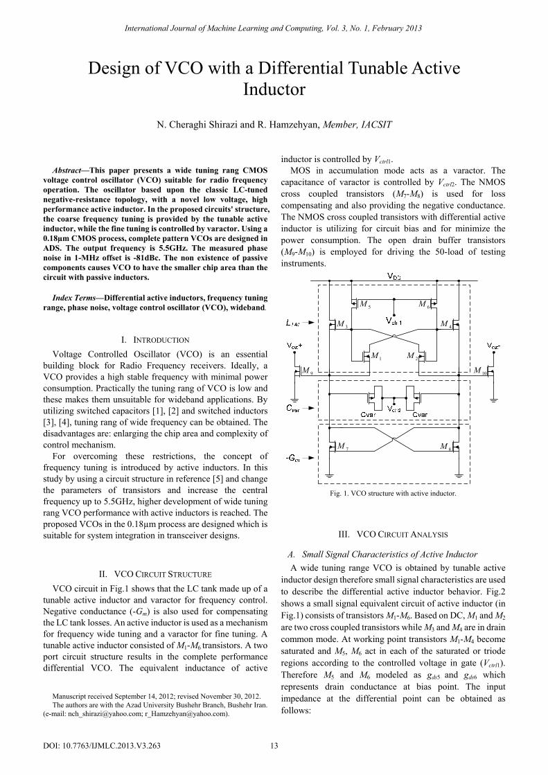
II. VCO CIRCUIT STRUCTURE VCO circuit in Fig.1 shows that the LC tank made up of a
tunable active inductor and varactor for frequency control. Negative conductance (-Gm) is also used for compensating the LC tank losses. An active inductor is used as a mechanism for frequency wide tuning and a varactor for fine tuning. A tunable active inductor consisted of M1-M6 transistors. A two port circuit structure results in the complete performance differential VCO. The equivalent inductance of active
Manuscript received September 14, 2012; revised November 30, 2012. The authors are with the Azad University Bushehr Branch, Bushehr Iran.
(e-mail: [email protected]; [email protected]).
inductor is controlled by Vctrl1. MOS in accumulation mode acts as a varactor. The
capacitance of varactor is controlled by Vctrl2. The NMOS cross coupled transistors (M7-M8) is used for loss compensating and also providing the negative conductance. The NMOS cross coupled transistors with differential active inductor is utilizing for circuit bias and for minimize the power consumption. The open drain buffer transistors (M9-M10) is employed for driving the 50-load of testing instruments.
1M 2M
3M
5M
4M
6M
8M7M
9M 10M
Fig. 1. VCO structure with active inductor.
III. VCO CIRCUIT ANALYSIS
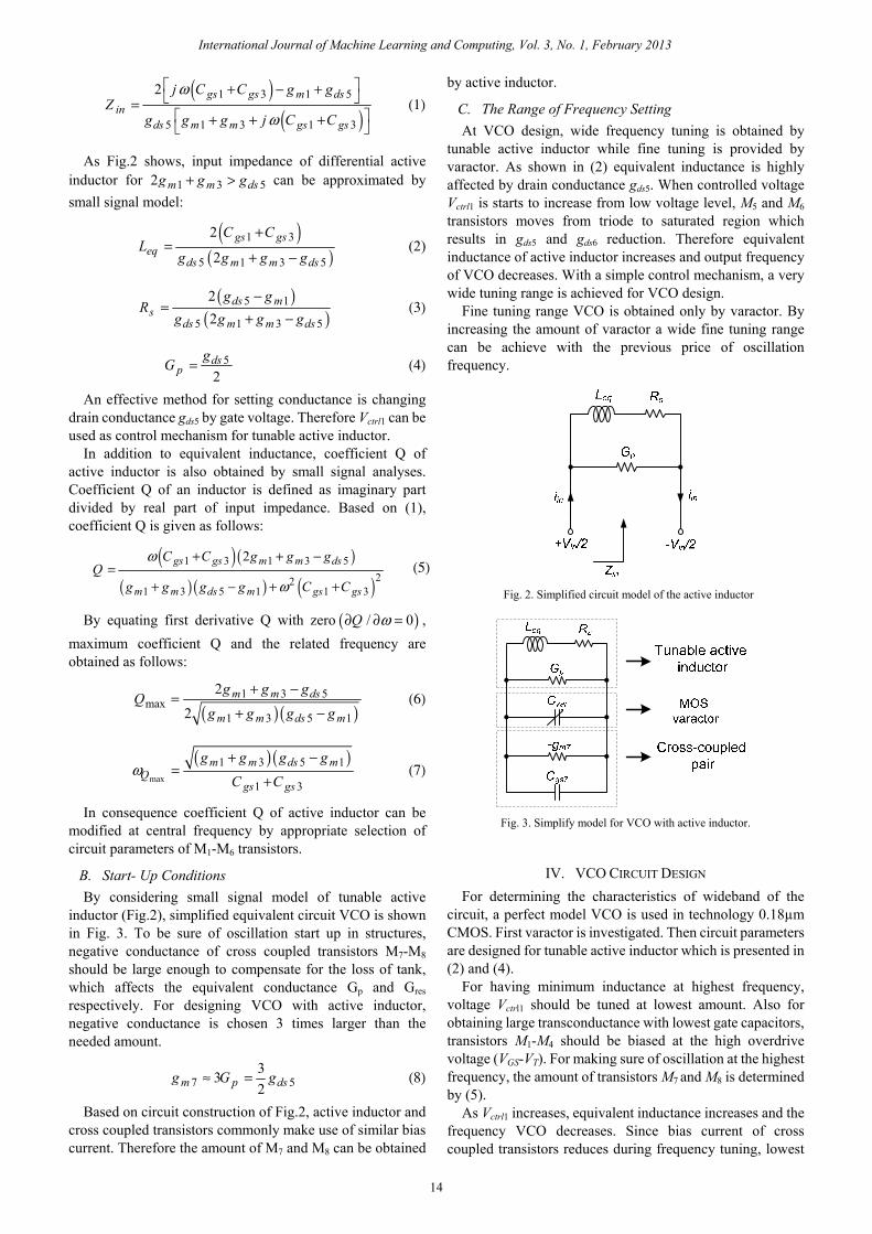
A. Small Signal Characteristics of Active Inductor A wide tuning range VCO is obtained by tunable active
inductor design therefore small signal characteristics are used to describe the differential active inductor behavior. Fig.2 shows a small signal equivalent circuit of active inductor (in Fig.1) consists of transistors M1-M6. Based on DC, M1 and M2 are two cross coupled transistors while M3 and M4 are in drain common mode. At working point transistors M1-M4 become saturated and M5, M6 act in each of the saturated or triode regions according to the controlled voltage in gate (Vctrl1). Therefore M5 and M6 modeled as gds5 and gds6 which represents drain conductance at bias point. The input impedance at the differential point can be obtained as follows:
Design of VCO with a Differential Tunable Active Inductor
N. Cheraghi Shirazi and R. Hamzehyan, Member, IACSIT
International Journal of Machine Learning and Computing, Vol. 3, No. 1, February 2013
13DOI: 10.7763/IJMLC.2013.V3.263
( )
( )1 3 1 5
5 1 3 1 3
2 gs gs m dsin
ds m m gs gs
j C C g gZ
g g g j C C
ω
ω
⎡ ⎤+ − +⎣ ⎦=⎡ ⎤+ + +⎣ ⎦
(1)
As Fig.2 shows, input impedance of differential active inductor for 1 3 52 m m dsg g g+ > can be approximated by small signal model:
( )( )
1 3
5 1 3 5
2
2gs gs
eqds m m ds
C CL
g g g g
+=
+ − (2)
( )
( )5 1
5 1 3 5
22
ds ms
ds m m ds
g gR
g g g g−
=+ −
(3)
52ds
pg
G = (4)
An effective method for setting conductance is changing drain conductance gds5 by gate voltage. Therefore Vctrl1 can be used as control mechanism for tunable active inductor.
In addition to equivalent inductance, coefficient Q of active inductor is also obtained by small signal analyses. Coefficient Q of an inductor is defined as imaginary part divided by real part of input impedance. Based on (1), coefficient Q is given as follows:
( )( )( )( ) ( )
1 3 1 3 522
1 3 5 1 1 3
2gs gs m m ds
m m ds m gs gs
C C g g gQ
g g g g C C
ω
ω
+ + −=
+ − + + (5)
By equating first derivative Q with zero ( )/ 0Q ω∂ ∂ = , maximum coefficient Q and the related frequency are obtained as follows:
( )( )
1 3 5max
1 3 5 1
2
2m m ds
m m ds m
g g gQ
g g g g
+ −=
+ − (6)
( ) ( )max
1 3 5 1
1 3
m m ds mQ
gs gs
g g g g
C Cω
+ −=
+ (7)
In consequence coefficient Q of active inductor can be modified at central frequency by appropriate selection of circuit parameters of M1-M6 transistors.
B. Start- Up Conditions By considering small signal model of tunable active
inductor (Fig.2), simplified equivalent circuit VCO is shown in Fig. 3. To be sure of oscillation start up in structures, negative conductance of cross coupled transistors M7-M8 should be large enough to compensate for the loss of tank, which affects the equivalent conductance Gp and Gres respectively. For designing VCO with active inductor, negative conductance is chosen 3 times larger than the needed amount.
7 5332m p dsg G g≈ = (8)
Based on circuit construction of Fig.2, active inductor and cross coupled transistors commonly make use of similar bias current. Therefore the amount of M7 and M8 can be obtained
by active inductor.
C. The Range of Frequency Setting At VCO design, wide frequency tuning is obtained by
tunable active inductor while fine tuning is provided by varactor. As shown in (2) equivalent inductance is highly affected by drain conductance gds5. When controlled voltage Vctrl1 is starts to increase from low voltage level, M5 and M6 transistors moves from triode to saturated region which results in gds5 and gds6 reduction. Therefore equivalent inductance of active inductor increases and output frequency of VCO decreases. With a simple control mechanism, a very wide tuning range is achieved for VCO design.
Fine tuning range VCO is obtained only by varactor. By increasing the amount of varactor a wide fine tuning range can be achieve with the previous price of oscillation frequency.
Fig. 2. Simplified circuit model of the active inductor
Fig. 3. Simplify model for VCO with active inductor.
IV. VCO CIRCUIT DESIGN For determining the characteristics of wideband of the
circuit, a perfect model VCO is used in technology 0.18µm CMOS. First varactor is investigated. Then circuit parameters are designed for tunable active inductor which is presented in (2) and (4).
For having minimum inductance at highest frequency, voltage Vctrl1 should be tuned at lowest amount. Also for obtaining large transconductance with lowest gate capacitors, transistors M1-M4 should be biased at the high overdrive voltage (VGS-VT). For making sure of oscillation at the highest frequency, the amount of transistors M7 and M8 is determined by (5).
As Vctrl1 increases, equivalent inductance increases and the frequency VCO decreases. Since bias current of cross coupled transistors reduces during frequency tuning, lowest
International Journal of Machine Learning and Computing, Vol. 3, No. 1, February 2013
14
frequency is obtained when negative conductance is low to compensating for the tank loss. After designing tunable active inductor, a varactor is chosen with maximum capacity 3pF for getting resonance frequency and gain of VCO.
In designing a wideband VCO using tunable active inductor, the phase noise is one of the important cases. The phase noise can be modified by increasing channel length of transistors.
1.2m 1.4m 1.6m 1.8m 2.0m 2.2m 2.4m1.0m 2.6m
600.f
800.f
1.00p
1.20p
1.40p
400.f
1.60p
W
C_F
ET
Fig. 4. The effect of changing W on capacitance
0.8 1.0 1.2 1.4 1.60.6 1.8
1.2p
1.3p
1.4p
1.5p
1.6p
1.1p
1.7p
Vctrl2
C_F
ET
Fig. 5. The effect of changing capacitance by varying voltage control
In this way extra parasitic capacitor reduces the range of tuning frequency and highest operating frequency. Therefore in this design, transistors MOS with minimum channel length is used to showing the range of optimized tuning for multi standard wireless applications.
V. SIMULATION For increasing the control frequency of VCO circuits up to
5.5GHz, some parameters of the circuit that can affect the frequency are chosen. For these purpose the capacitance and inductance of the circuit should be decreased. The capacitance can be reduced by varying the amount of W and L related to varactor.
In order to decrease the amount of active inductor, the control voltage of active inductor (Vctrl1) should be reduced, to increase the gds5 and gds6. By increasing gds5 and gds6, the inductance of active inductor is decreased, as presented in (2). Also the size of M1-M2 transistors has an effect on the amount of active inductor conductance. Therefore the active inductor conductance can also be controlled by varying W and L of this pair of transistors.
By reducing amount of inductor or capacitance, for providing oscillation condition the amount of negative resistance of the pair of cross coupled transistor, should also be taken in to consideration account. This amount of negative resistance can be control by varying the amount of W and L of pair of transistors.
The amount of transistors is given in Table I.
TABLE I: CIRCUIT PARAMETERS OF VCO
1 2,M M( )/m mμ μ
3 4,M M
5 6,M M
7 8,M M
30 / 0.18
25 / 0.18
112.5 / 0.18
70 / 0.18 After simulation, the amount of central frequency based on
the first harmonic is obtained 5.5GHz. MOS transistors are used as a voltage control capacitor
(varactor). MOS transistors act as a 2 port device (capacitor) with C capacitance, when drain, source and bulk are connected with each other [6].
As shown in Fig.4 by changing the length and width of transistors, the amount of capacitance can be varied. By increasing the amount of W and L, the capacitance is linearly enhanced. The curve of changing capacitance by varying control voltage is shown in Fig.5.
50 100 150 200 250 300 3500 400
0.6
0.8
1.0
0.4
1.2
time, psec
ts(o
utM
), V
ts(o
utP)
, V
Fig. 6. The output curve of VCO with active inductor
In this step the amount of Gm concerning active circuit should be compared with the amount of resonance circuit's conductance. The amount of Gm should be more than Gp in order to meet the condition of oscillation. The output curves of the circuit with active inductor are shown in Fig.6. The amount of phase noise of VCO is determined -80.314dBc in offset 1-MHz which are shown in Fig.7. The frequency fine tuning is achieved by the varactor. This amount of phase noise is obtained with Vctrl1=0.5V and Vctrl2=0.6V. If these control voltages change, the phase noise of the circuit and also the central frequency vary.
1E5 1E61E4 1E7
-100
-80
-60
-40
-120
-20
noisefreq, Hz
pnm
x, d
Bc
m2
m2noisefreq=pnmx=-80.31 dBc
1.000MHz
Fig. 7. Phase noise of VCO at 5.5GHz
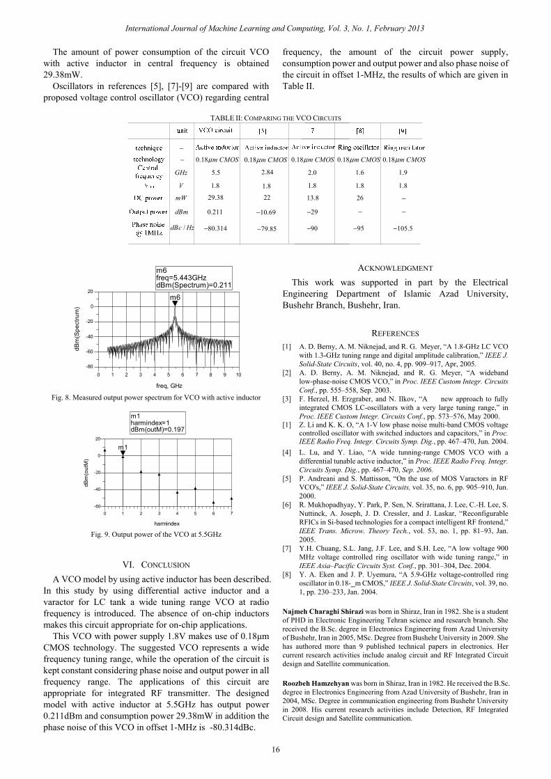
The amount of output power spectrum is also shown in
Fig.8. As shown in Fig.9, the output power is 0.197dBm in relation to the first harmonic.
International Journal of Machine Learning and Computing, Vol. 3, No. 1, February 2013
15
The amount of power consumption of the circuit VCO with active inductor in central frequency is obtained 29.38mW.
Oscillators in references [5], [7]-[9] are compared with proposed voltage control oscillator (VCO) regarding central
frequency, the amount of the circuit power supply, consumption power and output power and also phase noise of the circuit in offset 1-MHz, the results of which are given in Table II.
TABLE II: COMPARING THE VCO CIRCUITS
0.18 m CMOSμ 0.18 m CMOSμ 0.18 m CMOSμ 0.18 m CMOSμ
GHz 5.5 2.0 1.6 1.9
1.8 1.8 1.8 1.8V
mW 29.38 13.8 26 −
0.211 29−dBm − −
/dBc Hz 80.314− 90− 95− 105.5−
−
−
2.84
22
10.69−
79.85−
0.18 m CMOSμ
1.8
1 2 3 4 5 6 7 8 90 10
-60
-40
-20
0
-80
20
freq, GHz
dBm
(Spe
ctru
m)
m6
m6freq=dBm(Spectrum)=0.211
5.443GHz
Fig. 8. Measured output power spectrum for VCO with active inductor
1 2 3 4 5 60 7
-40
-20
0
-60
20
harmindex
dBm
(out
M)
m1
m1harmindex=dBm(outM)=0.197
1
Fig. 9. Output power of the VCO at 5.5GHz
VI. CONCLUSION A VCO model by using active inductor has been described.
In this study by using differential active inductor and a varactor for LC tank a wide tuning range VCO at radio frequency is introduced. The absence of on-chip inductors makes this circuit appropriate for on-chip applications.
This VCO with power supply 1.8V makes use of 0.18μm CMOS technology. The suggested VCO represents a wide frequency tuning range, while the operation of the circuit is kept constant considering phase noise and output power in all frequency range. The applications of this circuit are appropriate for integrated RF transmitter. The designed model with active inductor at 5.5GHz has output power 0.211dBm and consumption power 29.38mW in addition the phase noise of this VCO in offset 1-MHz is -80.314dBc.
ACKNOWLEDGMENT This work was supported in part by the Electrical
Engineering Department of Islamic Azad University, Bushehr Branch, Bushehr, Iran.
REFERENCES [1] A. D. Berny, A. M. Niknejad, and R. G. Meyer, “A 1.8-GHz LC VCO
with 1.3-GHz tuning range and digital amplitude calibration,” IEEE J. Solid-State Circuits, vol. 40, no. 4, pp. 909–917, Apr, 2005.
[2] A. D. Berny, A. M. Niknejad, and R. G. Meyer, “A wideband low-phase-noise CMOS VCO,” in Proc. IEEE Custom Integr. Circuits Conf., pp. 555–558, Sep. 2003.
[3] F. Herzel, H. Erzgraber, and N. Ilkov, “A new approach to fully integrated CMOS LC-oscillators with a very large tuning range,” in Proc. IEEE Custom Integr. Circuits Conf., pp. 573–576, May 2000.
[1] Z. Li and K. K. O, “A 1-V low phase noise multi-band CMOS voltage controlled oscillator with switched inductors and capacitors,” in Proc. IEEE Radio Freq. Integr. Circuits Symp. Dig., pp. 467–470, Jun. 2004.
[4] L. Lu, and Y. Liao, “A wide tunning-range CMOS VCO with a differential tunable active inductor,” in Proc. IEEE Radio Freq. Integr. Circuits Symp. Dig., pp. 467–470, Sep. 2006.
[5] P. Andreani and S. Mattisson, “On the use of MOS Varactors in RF VCO's,” IEEE J. Solid-State Circuits, vol. 35, no. 6, pp. 905–910, Jun. 2000.
[6] R. Mukhopadhyay, Y. Park, P. Sen, N. Srirattana, J. Lee, C.-H. Lee, S. Nuttinck, A. Joseph, J. D. Cressler, and J. Laskar, “Reconfigurable RFICs in Si-based technologies for a compact intelligent RF frontend,” IEEE Trans. Microw. Theory Tech., vol. 53, no. 1, pp. 81–93, Jan. 2005.
[7] Y.H. Chuang, S.L. Jang, J.F. Lee, and S.H. Lee, “A low voltage 900 MHz voltage controlled ring oscillator with wide tuning range,” in IEEE Asia–Pacific Circuits Syst. Conf., pp. 301–304, Dec. 2004.
[8] Y. A. Eken and J. P. Uyemura, “A 5.9-GHz voltage-controlled ring oscillator in 0.18-_m CMOS,” IEEE J. Solid-State Circuits, vol. 39, no. 1, pp. 230–233, Jan. 2004.
Najmeh Charaghi Shirazi was born in Shiraz, Iran in 1982. She is a student of PHD in Electronic Engineering Tehran science and research branch. She received the B.Sc. degree in Electronics Engineering from Azad University of Bushehr, Iran in 2005, MSc. Degree from Bushehr University in 2009. She has authored more than 9 published technical papers in electronics. Her current research activities include analog circuit and RF Integrated Circuit design and Satellite communication. Roozbeh Hamzehyan was born in Shiraz, Iran in 1982. He received the B.Sc. degree in Electronics Engineering from Azad University of Bushehr, Iran in 2004, MSc. Degree in communication engineering from Bushehr University in 2008. His current research activities include Detection, RF Integrated Circuit design and Satellite communication.
International Journal of Machine Learning and Computing, Vol. 3, No. 1, February 2013
16