Embed Size (px)
Citation preview

International Journal of Science and Research (IJSR) ISSN (Online): 2319-7064
Index Copernicus Value (2013): 6.14 | Impact Factor (2013): 4.438
Volume 4 Issue 7, July 2015
www.ijsr.net Licensed Under Creative Commons Attribution CC BY
Design of Transformer less Single Phase Inverter
for Renewable Energy Based Distribution
Generation System
T. Chandra Sekhar1, M.L.S. Deva Kumar
2, K. Vijaya Kumar Reddy
3
1M.Tech student, Dept of Mechanical Engineering JNTUACEA Ananthapur, India 2Professor of Mechanical Engineering JNTUA College of Engineering, Ananthapur, India 3Professor of Mechanical Engineering, JNTUH college of Engineering, Hyderabad, India
Abstract: Solar energy is the major source of power. Its potential is 178 billion MW which is about 20,000 times the world’s demand.
Solar energy, received in the form of radiation (electromagnetic waves), can be converted directly or indirectly into other forms of
energy, such as heat and electricity which can be utilized by man .Inverters are the devices usually solid state which change the array
DC output to AC suitable voltage, frequency and phase to feed photo voltaic ally generated power into the power grid or local load. Solar
energy is time dependent and intermittent energy resources. Inverter may also contain a suitable output step up transformer perhaps
some filtering and power factor correction circuits and some power conditioning circuitry to initiate the battery charging and to prevent
overcharging .Inverters of PV system based distributed generation (DG) are subjected to wide changes in the inverter input voltage, thus
demanding a buck-boost operation of inverters . Further the inverter size, weight and cost is increased. It is designed transformer less
inverter that can be operated over a wide dc input voltage range making it suitable for distributed generation applications. Depending on
the reference signal the inverter output voltage can be either boosted or bucked with respect input voltage.
Keywords: Distribution Generation Systems (DG), Buck-Boost inverter, Reference signal, transformer less inverters, PWM.
1. Introduction
Renewable energy substitutes conventional fuels or distinct
areas air and water heating and cooling, motor fuels,
electricity generation. Photovoltaic systems (PV) that supply
power directly to the grid are becoming more popular due to
the cost reduction achieved from the lack of a battery
subsystem. This design can be used in high power ranges
providing high system flexibility [1].
Energy conversion devices which are used to convert sun
light to electricity by the use of the photo voltaic effect are
called “Solar cells”. Inverters are the devices usually solid
state which change the array DC output to AC suitable
voltage, frequency and phase to feed photo voltaic ally
generated power into the power grid or local load. Inverter
may also contain a suitable output step up transformer for
some filtering and power factor correction circuit.
Distributed generation (DG) systems are usually small
modular devices which are nearly to electricity consumers.
These include wind turbines, solar energy systems, fuel
cells, micro gas turbines, and small hydro systems, as well
as relevant control and energy storage systems. These
systems normally need inverters as interfaces between their
single phase loads and source [3].
Figure 1: Renewable Energy Based DG system
The functions of inverters for small DG systems can be
summarized as follows [2].
1) It converts power conversion from variable dc voltage
into fixed ac voltage for stand-alone applications and ac
output in synchronism with the grid voltage and
frequency for grid-connected applications.
2) Variable dc voltage can be higher or lower than the ac
voltage in a system, which is observed normally in a
solar energy and wind turbine systems. Thus, there is a
need to buck boost the inverter voltage.
Based on the electrical isolation between the output and
input, inverters can be classified as isolated or non isolated.
Electrical isolation is normally achieved using either line-
frequency or high-frequency transformers [1]. Inverters are
used for many applications, as in situations where low
voltage DC sources such as batteries, solar panels or fuel
cells should be converted so that devices can run off of AC
power.
2. Literature Survey
The dc link voltage of inverters for DG systems may vary
over a wide range. Depending upon the input dc voltage
range in comparison to the output ac voltage, inverters can
be buck inverters, boost inverters, or buck-boost inverters.
Different dc voltages are applied to the inverter input
because of the renewable energy sources, such as solar
batteries and fuel cells, which produce different dc-voltage
levels [4].Normally, most topologies are boost or buck–
boost due to two main factors. First one, pulse width
modulation (PWM) produces an output voltage lower than
the dc link voltage therefore, the dc link should be greater
than the maximum possible ac output voltage. Second one,
sometimes, independent of frequency, voltage step-up is
necessary [5].
Paper ID: SUB156420 740
International Journal of Science and Research (IJSR) ISSN (Online): 2319-7064
Index Copernicus Value (2013): 6.14 | Impact Factor (2013): 4.438
Volume 4 Issue 7, July 2015
www.ijsr.net Licensed Under Creative Commons Attribution CC BY
The transformer used for an inverter is a step-up type.
Transformer must have very low resistance because of the
high current involved, and in all cases transformer has to be
designed for the mains frequency in use. This means that it
will be comparatively large, at least the same size as a
normal step-down transformer used for the same VA rating.
Depending on the intended usage (permanently or
intermittent connected for example) the allowable losses will
be different. A transformer that will only be used for normal
UPS duties may be smaller than the ideal case, and it will
therefore be cheaper, smaller and lighter. Of course, it will
also have higher losses. The primary inductance is of little
real consequence, but it must be high enough to ensure that
magnetizing current at 50Hz or 60Hz is low enough to
ensure losses are within sensible limits.
Figure 2: Block Diagram DC to AC
The boost converter is best if a significant and much step up
is required, such as with a short string of 12-PV panels [6].
A cascaded multilevel inverter consists of a series of H-
bridge inverter devices. The work of multilevel inverter is to
synthesize a desired voltage from Several Separate DC
Source [6]. The main disadvantage of this system is that
each single H-bridge cascaded inverter modules needs a
separate DC supply source [9].
Traditional full-bridge inverters do not have flexibility of
handling a wide range of dc input voltages. Especially when
the DC voltage is lower than the AC voltage, heavy line-
frequency step-up transformers are required. Although these
inverters show robust performance and high reliability, they
demand higher volume, weight and cost for DG system
applications [7].
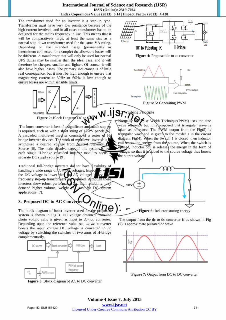
3. Proposed DC to AC Converter
The block diagram of boost inverter used for the proposed
system is shown in Fig 3. DC voltage obtained from the
photo voltaic cells is given as input to dc- dc converter.
Depending upon the reference value set, dc-dc converter
boosts the input voltage DC voltage is converted to ac
voltage by switching the switches of two arms of H-bridge
complementarily.
Figure 3: Block diagram of AC to DC converter
Figure 4: Proposed dc to ac converter
Figure 5: Generating PWM
3.1 Working Principle
Normally the Pulse Width Technique(PWM) uses the sine
wave reference but it is proposed that triangular wave is
taken as reference .The PWM output from the Fig(5) is
triangular wave and is given to the mosfet 1 in the circuit
diagram Fig(4). When the Switch 1 is closed .then inductor
coil stores the energy from the source, When the switch is
opened, inductor coil is releases the energy in the form of
voltage, so that it is added to the source voltage thus boosts
the output voltage.
Figure 6: Inductor storing energy
The output from the dc to dc converter is as shown in Fig
(7) is approximate pulsated dc wave.
Figure 7: Output from DC to DC converter
Paper ID: SUB156420 741

International Journal of Science and Research (IJSR) ISSN (Online): 2319-7064
Index Copernicus Value (2013): 6.14 | Impact Factor (2013): 4.438
Volume 4 Issue 7, July 2015
www.ijsr.net Licensed Under Creative Commons Attribution CC BY
Figure 8: Output wave from H-Bridge
This pulsated dc wave is given to the H Bridge inverter as
shown in the Fig (8). The output from the dc to dc converter
is fed to the H Bridge which is cosists of four Mosfets.
Figure 9: H-Bridge schematic diagram
The implementation of this circuit is done. The system
Parameters of the circuit to generate triangular wave from
integrated circuit logic inverter 74hc14 are in table (1).
Table 1: System parameters Power frequency Capacitance Resistance
60Hz .1uf 200 ohms
50Hz .1uf 176 ohms
The proposed design of the inverter is implemented using
boost converter and PWM generator .The input voltage is
varied from 1Vto 30V. The output voltage is varied from 85
to 105V (lower rated devices used for implementation,
XL6009 voltage regulator) with corresponding input
voltage. The circuit working is examined are in table (2).
Figure 9: Experimental setup
4. Results
It is implemented and validated the proposed design of
circuit .The summary of results are given in table (2).
Table 2: Summary of results S No Vin(V) V out(V)
1 1 0
2 2 45
3 3 67
4 4 96
5 5 105
6 6 105
7 12 105
In this case the proposed design of the inverter circuits acts
as a boost inverter since the reference triangular wave is set
to maximum, so that voltage is constant. The implemented
inverter acts as boost inverter converting 10 volts to 105
volts. It is observed that the output voltage is remains same
when further increase in input voltage from 5V.
5. Conclusion
From the results it is seen that designed boost single phase
voltage inverter works well producing an ac wave outputs
depending upon the reference signal. From the summary
table it can be summarized that proposed design of the
inverter circuit operates for wide voltage range of the dc
input voltage producing a sinusoidal ac voltage 50Hz.
The proposed design uses only five switches, the low
switching frequency of the output H-bridge reduces the
inverter switching losses and cost compared to multilevel
inverters.
The drawbacks of the inverter, compared to traditional H
Bridge inverters are relatively high cost (switches) and
relatively high switching losses in one of the five switches.
6. Scope of Future Work
The present trend of research, the cost of photovoltaic cells
is expected to go down in future. This design of inverter
under consideration is capable of minimizing the no of
components and design portable, thus occupying less space
reducing the size of the equipment. This design can be
extended by using suitable inductor coils and switching
circuitry.
References
[1] T. G.Wilson, “The evolution of power electronics,”
IEEE Trans. Power Electron., vol. 15, pp. 439–446,
May 2000.
[2] Channaveer.P.Malad , K.Uma Rao” Simulation Of a
Buck-Boost Single Phase Voltage Source Inverter for
Distribution Generation Systems” International Journal
of Modern Engineering Research (IJMER),Vol.2,
Issue.5, Sep.-Oct. 2012 pp-3628-3632.
[3] Roman, I.T. “A single-phase current-source inverter with
active power filter for grid-tied PV systems”, 3rd IEEE
International Symposium on Power Electronics for
Paper ID: SUB156420 742

International Journal of Science and Research (IJSR) ISSN (Online): 2319-7064
Index Copernicus Value (2013): 6.14 | Impact Factor (2013): 4.438
Volume 4 Issue 7, July 2015
www.ijsr.net Licensed Under Creative Commons Attribution CC BY
Distributed Generation Systems (PEDG), Aalborg, pp.
349-356, June 2012.
[4] Ahmed Mohamed Salamah, Stephen J. Finney “Single-
Phase Voltage Source Inverter with a Bidirectional
Buck–Boost Stage for Harmonic Injection and
Distributed Generation” IEEE transactions on power
electronics, vol. 24, no. 2, pp 376- 387, February 2009.
[5] R. Gonzalez, E. Gubia, J. Lopez, and L.Marroyo,
“Transformerless single phase multilevel-based
photovoltaic inverter,” IEEE Trans. Ind. Electron., vol.
55, no. 7, pp. 2694–2702, Jul. 2008.
[6] Geoffrey R. Walker, Member, IEEE, and Paul C. Sernia
IEEE TRANSACTIONS ON POWER ELECTRONICS,
VOL. 19, NO. 4, JULY 2004 Cascaded DC–DC
Converter Connection of Photovoltaic Modules.
[7] X. Yaosuo, C. Liuchen, B. K. Kjaer, J. Bordonau, and T.
Shimizu, “Topologies of single-phase inverters for small
distributed power generators: An overview,” IEEE
Trans. Power Electron., vol. 19, no. 5, pp. 1305–
1314,Sep. 2004.
[8] M. Calais, J. Myrzik, T. Spooner, V. G. Agelidis,
“Inverter for Single-Phase Grid Connected Photovoltaic
Systems – An Overview,” Power Electron. Spec. Conf.,
Vol. 4, pp. 1995-2000, Feb. 2002.
[9] Jaydeep Lakwal*, D. M. Deshpande, Arisutha Suresh,
Arvind Mittal,” Cascaded Multilevel Inverter Topologies
for Photovoltaic Power Generation Systems”
International Journal of ChemTech Research CODEN (
USA): IJCRGG , Vol.5, No.2, pp 1094-1100, April-June
2013.
[10] R. Ramos, D. Biel, E. Fossas and F. Guinjoan, “A Fixed-
Frequency Quasi-Sliding Control Algorithm: Application
to Power Inverters Design by Means of FPGA
Implementation,” IEEE Trasn. Power Electro., vol. 18,
no 1, pp. 344-355, Jan.2003.
Author Profile
T.Chandra Sekhar M.Tech , Dept of Mechanical
Engineering JNTUACEA Ananthapur, India
M.L.S. Deva Kumar M.TECH, MBA, Ph.D,
Professor at Dept of Mechanical Engineering in
JNTUA College of Engineering in ANANTAPUR,
Andhra Pradesh, India.
K. Vijaya Kumar Reddy Professor of Mechanical Engineering,
JNTUH college of Engineering, Hyderabad.
Paper ID: SUB156420 743