Embed Size (px)
Citation preview

DESIGN OF MULTIPLIER AND
ITS VLSI IMPLEMENTATION
by
QI LIU, B.S., B.A., M.E., M.S.
A THESIS
IN
ELECTRICAL ENGINEERING
Submitted to the Graduate Faculty of Texas Tech University in
Partial Fulfillment of the Requirements for
the Degree of
MASTER OF SCIENCE
IN
ELECTRICAL ENGINEERING
AoDroved
May, 1999

80S 73
QQQ ACKNOWLEDGEMENTS
C.0/0 ly ^ would like to express my appreciation to my committee chair. Dr. Micheal
Parten, for his guidance and support during my research and writing of my thesis.
I also would like to thank my committee members. Dr. Sunanda Mitra and Dr.David
Mehrl for their precious time and help, and the Department of Electrical Engineering of
Texas Tech University for supporting my studies.
I also would like to express my appreciation to my parents and wife for their help,
encouragement and love.
11

BHBsessanss
TABLE OF CONTENTS
ACKNOWLEDGMENTS ii
ABSTRACT v
LIST OF TABLES vi
LIST OF FIGURES vii
CHAPTER
I. INTRODUCTION 1
1.1 Evolution of Building Block for Digital Systems 1
1.2 The Evolution of Bit-Slice device 3
1.3 Objectives 9
II. MULTIPLIERS: OVERVIEW 10
III. MULTIPLICATION ALGORITHM AND 13
3.1 Direct Multiplication of Two Unsigned Binary Numbers 13
3.1.1 Sequential Multiplier 13
3.1.2 Parallel Adders Array Multiplier 15
3.2 Direct Multiplication of Signed Binary Numbers 17
3.3 3 -bit Recoding Algorithm for Multiplication 19
IV. IMPLEMENTATION OF PARALLEL TWO'S COMPLEMENT MULTIPLIER 22
4.1 Architecture of an 8 x 8 bit multiplier 22
4.2 Two's Complement Block 23
4.3 3-bit Encoder Block 26
iii

4.4 The Partial Product Selector 27
4.5 Carry Save Adders Array Block 28
4.6 Ripple Carry Adders 29
4.7 Carry Select Adders 29
4.8 16 X 16 bit Multiplier 30
V. LAYOUT OF CMOS MULTIPLIER INTEGRATED CIRCUITS 32
5.1 Overview of Integrated Circuits 3 2
5.2 Design Philosophies 32
5.3 The Floorplan 33
5.4 Interconnections 34
5.5 Floorplan and Physical Layout of the Multiplier Chip 35
VI. PSPICE SIMULATION AND CHIP TEST 38
6.1 Pspice Simulation of Schematic Multiplier Circuits 38
6.2 Discussions of Pspice Simulation Results 48
6.3 Post-Layout Simulation Results 49
6.4 Chip Test Results 54
6.5 Comparison of Post Layout Simulation and Chip Test Results 60
VII. CONCLUSIONS 61
REFERENCES 63
IV

•^-^t^i. " - " " — " ^ ' " n — . . - « . . « » . w , . . f . . ^ ^ » . . . . . .
ABSTRACT
A 3-bit recoding algorithm is used to implement a parallel multiplier in two's
complement. The circuits at gate level for implementing 8 x 8-bit multiplier are
presented. To obtain highest speed, (1) carry skip adders combined with carry select
adders are adopted to implement two's complement multiplier, (2) carry save adders
combined with carry select adders are used to add partial products. An 8x8-bit multiplier
was implemented physically with 1.2^m CMOS SCN (Scaleable N-well) technology
using Tanner L-Edit CMOS layout tool. The area of the chip (not including pads frame)
is 1 mm . The chip has been fabricated and tested. From the chip test, the execution time
is less than 5.7ns. A 16x16-bit multiplier implemented with 8x8-bit multiplier cells using
Pspice software tool was also presented. The execution time of the 16x16-bit multiplier is
about 1.5 times that of the 8x 8-bit multiplier from the Pspice simulation.

—'-IIIIIWIIII——MIIIIIII mi l l r:- - _ i ^ — > • ':•• MUBi^iVinTrnniiaftaaamwajB
LIST OF TABLES
3.1 3-bits recoding 20
4.2 Encoder 26
VI

r^^^^^^^—i^n i^n^^fc - ' i r "t" i iiwii'irii'iiianiiniriitmnHiiiiniiii • 1—n—~°
LIST OF FIGURES
1.1 Typical processing-section organization 5
1.2 Three-dimensional view of a typical processing section 6
1.3 A vertical slice through the processing section 7
1.4 The RTL Architecture for the TMS320C10 8
3.1 Digital multiplication of unsigned four bit binary numbers 13
3.2 Flow chart for multiplication process of a sequential multiplier 14
3.3 4 x 4 array multiplier 16
3.4 Half adder and Full adder 17
3.5 Digital multiplication of 4-bit two's complement binary numbers 18
3.6 Two's Complement Sequential Multiplier Hardware 19
4.1 Parallel multiplier of the 8 x 8-bit multiplier 22
4.2 Two's Complement Circuit 24
4.3 Partof 3-bit encoder circuit 27
4.4 Circuit to determine i bit of the k partial product 28
4.5 Carry save adders arrays 28
4.6 Ripple carry adders 29
4.7 Carry select adders array 30
4.8 Adders Array of 16 x 16 bit multiplier 31
5.1 Floorplan and pin arrangements of the multiplier chip 36
5.2 Physical layout of the chip 37
6.1 Schematic circuit of the 8 x 8 multiplier 38
vii

^^•'*^*^--''^*<^^^B^^^^^^^^fc^'.::±n!MeiaiJJjJU'Ju6£i5£[l!ii^0.>^i,.«f (• --. .— ^~- . „ , , . . . . ^ ^-
6.2 Voltage levels of output P with X=00001 lOh and ¥=000010012 40
6.3 Voltage levels of output P with X=l 111001 h and Y=0000100l2 43
6.4 Voltage levels of output P with X=l 11100112 and ¥=1111011 h 43
6.5 Voltage levels of output P with X=000010112 and ¥=111101112 44
6.6 Output P with X=0000000000001 IOI2 and ¥=00000000000010012 45
6.7 Output P with X=l 1111111111100112 and ¥=00000000000010012 46
6.8 OutputPwith X=111111111111001l2and¥=111111111111011l2 47
6.9 Output P with X=0000000000001 IOI2 and ¥=111111111111011 h 48
6.10 The output P=000000000111010l2 50
6.11 The output P=l l l 11111100010112 51
6.12 The output P=00000000011IOIOI2 52
6.13 The output P=ll 111IIIIOOOIOII2 53
6.14 Chip Test Configuration 54
6.15 Inputs Xi , ¥1 and output P of the chip 56
6.16 Output of the chip with inputs X1 and ¥ 1 57
6.17 Inputs X2 and ¥2 of the chip 58
6.18 Output of the chip with input X2 and ¥2 59
Vlll

" — - - - - ~ ~ " ~ — • —^-nr^r^n^'-'ww^
CHAPTER I
INTRODUCTION
1.1 Evolution of Building Blocks for Digital Systems
In the past 60 years, the development of digital computers has gone through four
generations. Digital computers are generic processors. Over the past decade, application
specific processors (ASIC) such as digital signal processors have been developed quickly
from the technological advances in integrated circuit design and fabrication. Both
generic and ASIC processors are complex digital systems. The designs of these modem
digital systems are based on building blocks. System engineers design the architecture of
digital systems and determine the interconnection of devices such as adders, registers,
arithmetic logic units (ALU), multipliers, multiplexers, and memory arrays to form
digital systems. The circuit and logic designers design these building blocks. The
advantages of using basic building blocks to design complex systems include shorter
design times, lower cost, higher reliability, higher speeds and more flexibility.
The development of building blocks has been going on for roughly four
generations [1]. Not only did each generation introduce significant improvements in
component speed, cost, and reliability, but they also significantly improved the
productivity of the system design and manufacturing processes.
The traditional types of design include the following:
1. Circuit design - the interconnection of discrete components such as transistors,
resistors, and capacitors, to form logic devices such as ANDs and ORs.
2. Logic design ~ the interconnection of logic devices to form combinatorial emd
• I wm '—J*. "'™™'^~'~"^°'~"'7~"TTii'mMa'nHnrrTT'
sequential devices such as registers, counters, and adders.
3. System design ~ the interconnection of such devices as adders, registers, and memory
arrays to form digital systems such as processors and I/O device controllers.
4. Physical design - the physical layout of the components, for instance, on printed
circuit or wire-wrap boards.
The building blocks of the first technology generation, beginning in the 1940s and
lasting into the early 1960s, were discrete components such as transistors (earlier,
vacuum tubes), diodes and resistors. At that time, engineers were faced with the full tasks
of circuit, logic, system, and physical design.
The second generation, occurring in the early- and mid-1960s, saw the building
blocks grow into integrated circuits, each of which contained from 10 to 50 elementary
components and performed such logic functions as AND and NOR. The jobs of logic and
system design remained the same, but the task of circuit design was greatly reduced, and
the task of physical design was reduced somewhat, since the integrated circuit reduced
the total part count of a system.
The building blocks of the third generation, occurring in the late 1960s and early
1970s, were medium scale integrated circuits (MSI) representing logic devices containing
from 50 to 200 elementary components and forming such devices as registers, counters,
multiplexers, and arithmetic logic units (ALU). This generation continued the reduction
of the task of physical design (again because of a reduction in the number of physical
parts needed to build a system) and lessened the task of logic design.

imtm»mmmm^^t*f9¥Ct
The fourth generation, which began in the early 1970s, brought about an immense
leap in the size and scope of the building blocks. One notable change occurred in storage
devices. Single chips containing 4kB bits of storage, and later, 16kB and 64kB chips
became widely available. Another notable change was the microprocessor. On one chip,
embodied in 20,000 or more elementary components, is a full-fledged central processing
unit and perhaps a small amount of memory.
Given that a microprocessor and its support chips (e.g., disk controllers, keyboard
controllers, communication interfaces, memory-refresh logic, bus controllers) can be
used, the tasks of digital system design and physical layout are substantially reduced,
however, the microprocessor is not a viable solution to all design problems. Commercial
microprocessors can be relatively slow and have static and sometimes primitive
instruction sets. This has led to the development of application specific processors.
1.2 The Evolution of Bit-Slice device
Fourth-generation building blocks are very large scale integration (VLSI) devices.
The motivation behind VLSI is lower cost, higher speeds, higher reliability and shorter
design times. However, the designer of VLSI devices now faces two new problems: the
"pin-out" problem and the "part-proliferation" problem. A typical VLSI silicon chip may
have a size of 0.15 x 0.2 inches. Obviously only a limited number of external connections
can be made between this chip and the outside world. Currently the feasible upper limit is
in the neighborhood of 100 to 300 connections (pins on the package holding the chip),
and it is unlikely that significant increases in this limit will be made. This restricts the
type of circuitry that can be placed on a chip.
3
— •aSBI
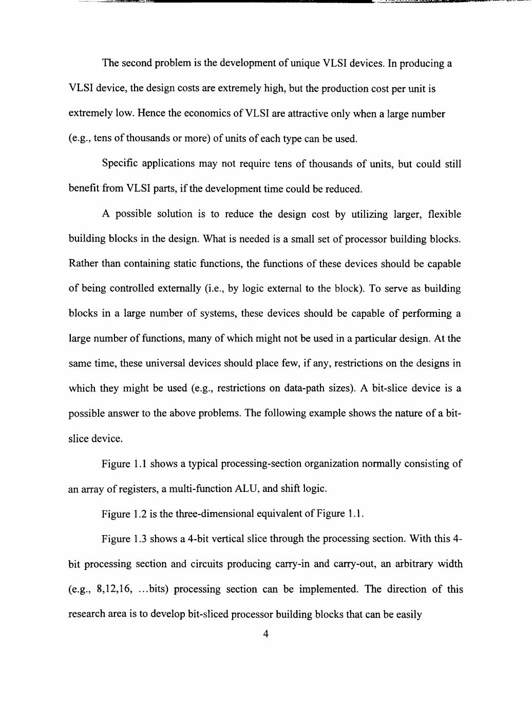
The second problem is the development of unique VLSI devices. In producing a
VLSI device, the design costs are extremely high, but the production cost per unit is
extremely low. Hence the economics of VLSI are attractive only when a large number
(e.g., tens of thousands or more) of units of each type can be used.
Specific applications may not require tens of thousands of units, but could still
benefit from VLSI parts, if the development time could be reduced.
A possible solution is to reduce the design cost by utilizing larger, flexible
building blocks in the design. What is needed is a small set of processor building blocks.
Rather than containing static functions, the functions of these devices should be capable
of being controlled externally (i.e., by logic external to the block). To serve as building
blocks in a large number of systems, these devices should be capable of performing a
large number of functions, many of which might not be used in a particular design. At the
same time, these universal devices should place few, if any, restrictions on the designs in
which they might be used (e.g., restrictions on data-path sizes). A bit-slice device is a
possible answer to the above problems. The following example shows the nature of a bit-
slice device.
Figure 1.1 shows a typical processing-section organization normally consisting of
an array of registers, a multi-function ALU, and shift logic.
Figure 1.2 is the three-dimensional equivalent of Figure 1.1.
Figure 1.3 shows a 4-bit vertical slice through the processing section. With this 4-
bit processing section and circuits producing carry-in and carry-out, an arbitrary width
(e.g., 8,12,16, ...bits) processing section can be implemented. The direction of this
research area is to develop bit-sliced processor building blocks that can be easily
4

r T i i " ' » » » w i . i * > H » , ; * , ,,-Jl- —•_". l\-_- .-_._
Figure I.l Typical processing-section organization
— iiimTn-fii-'i'Tiiwd riiiVi •-"'g'^'"rT."i.:',")r.V" '—'—-\f>-. '•" J^TpLXi jJjrT.TTT:
Figure 1.2 Three-dimensional view of a typical processing section

Shifter connection
Figure 1.3 A vertical slice through the processing section
•••".".'jixaanux
A11-A0/ PA2-PA0 01S-00
Legend: AGO a Accumulator ALU -Arithmetic Logic Unit ARP - Auxiliary Register Pointer ARO > Auxiliary Register 0 AR1 -Auxiliary Register 1 OP - Data Page Pointer P - P Register PC -Program Counter T - T Register
Figure 1.4 The RTL Architecture for the TMS320C10
8

1 "iifit^iLa i> t 'vi*
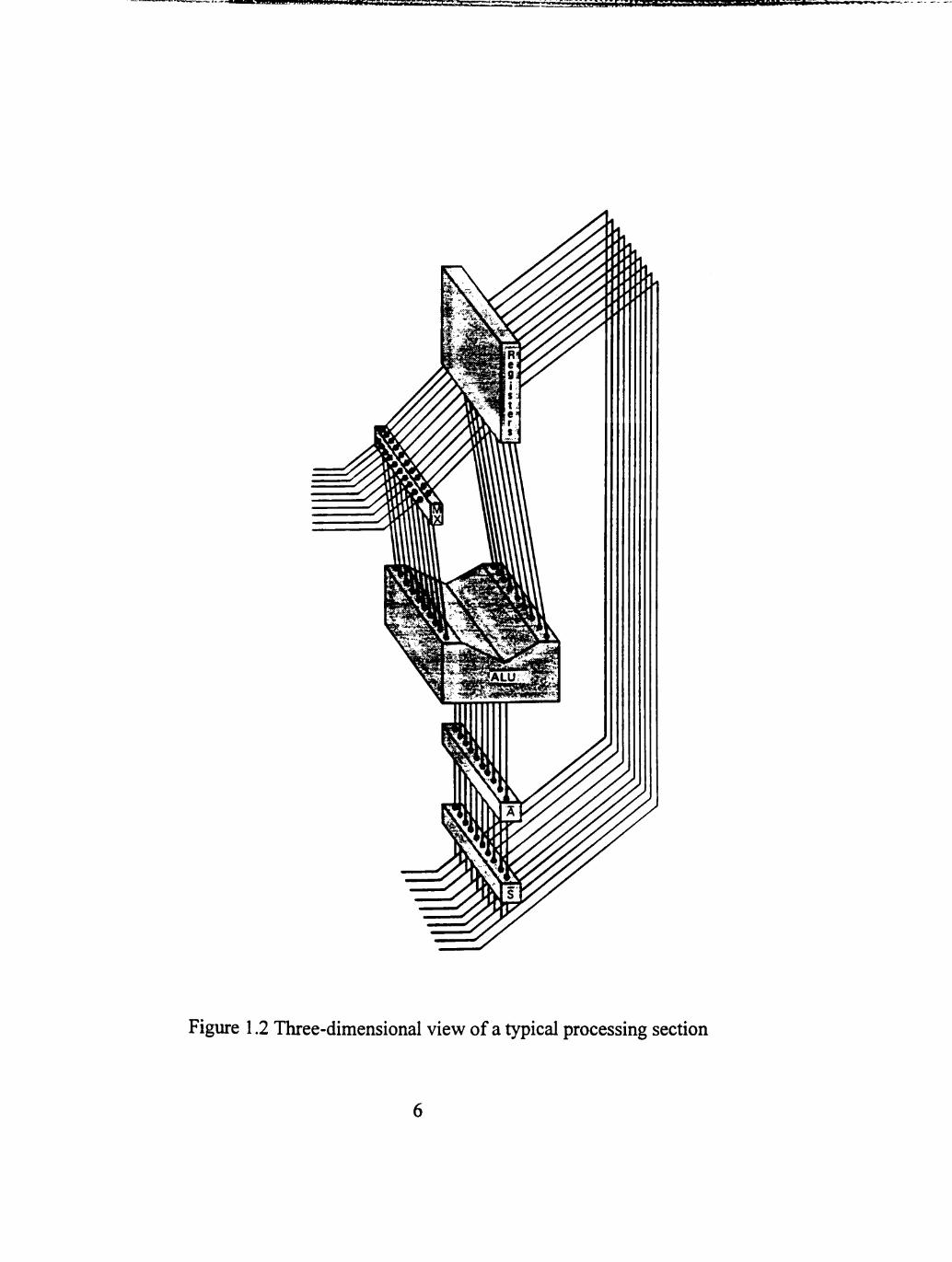
Both generic and ASIC processors usually have a unit that can implement
arithmetic operations. One of the important arithmetic operations is the multiplication
operation. In many modern digital systems, multiplication is implemented by using a
hardware multiplier. It is one of the important parts of many digital systems. The design
of high speed hardware multipliers has been an active research subject. Figure 1.4 shows
the RTL architecture for the TMS320C10 [2] with a hardware multiplier.
1.3 Objectives
The objective of this research is to design and implement a high performance
CMOS multiplier bit-slice building block. Combined with other blocks, for example.
Arithmetic Logic Unit (ALU), Control Units, Registers, Multiplexers, Accumulators, etc;
both generic and application specific (ASIC) processors can be implemented and tested.
First, an 8 X 8 bit multiplier is designed and implemented, and then, a 16 x 16 bit
multiplier is implemented using 8 x 8 bit multiplier cells and other circuits. The focus of
the design is on both performance and reduced chip area.
The Chapter II gives an overview of multipliers. Chapter III describes algorithms
for multiplication and implementations. Chapter IV introduces CMOS multiplier circuit
layout. Chapter V shows a Pspice simulation and the multiplier chip test results. Chapter
VI gives the conclusion.

mmitim i i iimn
CHAPTER II
MULTIPLIERS: OVERVIEW
Muhipliers can be classified as hardware multipliers and software multipliers. In
older digital systems, there was no hardware multiplier and multiplication was
implemented with a microprogram. The microprogram needed many micro instruction
cycles to complete the multiplicafion process, which make the microprogrammed
multipliers slow. For high speed digital systems, hardware multipliers are usually used. In
modem microprocessors and ASIC processors, most arithmetic logic units (ALU) contain
a hardware multiplier. High speed hardware multipliers have been of interest for
sometime. More sophisticated approaches for multiplier designs can be implemented
today due to the increase density of integrated circuits.
Hardware multipliers can be divided in two main categories: sequential and
parallel array multipliers. For a sequential multiplier [3], multiplication of the multiplier
and multiplicand is the operation of repeatedly adding the multiplicand and shifting. The
advantage of a sequential multiplier is that the circuit is simple and the chip occupies less
area, the disadvantage is that it is slower. For parallel array multipliers, the summation of
partial products is carried out by using a linear adder array. Because the operation is in
parallel, the speed is much faster than of a sequential multiplier.
There are a number of algorithms used for multiplication [4,5,6]. The 3-bit
recoding algorithm is one of the most well known . It is used in the design of many kinds
of hardware and software multipliers. This algorithm is used to reduce the number of
partial product rows by about half, so, the speed of multiplication increases significantly
10

and the chip area is reduced. The 3-bit recoding algorithm is also called the Modified
Booth's Algorithm and was developed from Booth's algorithm [7]. A number of other
multiple-bit recoding algorithms for multiplication have been developed [8]. Recenth, a
parallel hardware multiplier based on a 5-bit recoding algorithm has been proposed [9].
From the view of optimization, the 5-bit recoding algorithm is preferred to a 4-bit
recoding algorithm. While more partial product rows can be reduced with the 5-bit
recoding algorithm than with a 3-bit recoding algorithm, more complicated circuits are
required to determine the odd multiples of the multiplicand. With the potential of
improving both performance and the hardware requirements, the 5-bit recoding algorithm
maybe good for a high bit multiplier, but, not for a low bit multiplier, such as, an 8 x 8 bit
multiplier.
Using the 5-bit recoding algorithm reduces the number of partial product
rows to two. The partial products are selected from 17 different multiples of the
multiplicand Y (0, ± Y, ± 2Y, ± 3Y, ± 4Y, ± 5Y, ± 6Y, ± 7Y, ± 8Y). Using the 3-bit
recoding algorithm reduces the number of partial product rows to four. The partial
products are selected from 5 different multiples of the multiplicand Y (0, ± Y, ± 2Y).
The addition of four partial products can be changed to the addition of two binary
numbers by using two rows of carry save adder arrays (CSA) with only a two gate delay
introduced. The even multiples of the multiplicand Y can be implemented by using a
hardwire shift. For the 3-bit recoding algorithm, only the two's complement of Y needs to
be determined. For the 5-bit recoding algorithm, additional high speed adders are
required to determine odd multiples of Y. These high speed adders require more circuitry
11

to implement and suffer more time delay. For higher bit multipliers, the advantage of the
5-bit recoding algorithm can be seen. For example, for a 32 x 32 bit multiplier, the 5-bit
recoding algorithm reduces the number of partial product rows to 8 and the 3-bit recoding
algorithm reduces the number of partial product rows to 16. The reduction of the number
of partial product rows is apparent.
The 3-bit recording algorithm is used here because our objective is to build an
8 X 8 bit multiplier block. With this block, higher bit multipliers can be built.
12

iU I I I . I M I I « H « » I I I U • I I r a . . .
CHAPTER III
MULTIPLICATION ALGORITHMS AND HARDWARE
3.1 Direct Multiplication of Two Unsigned Binary Numbers
The process of digital multiplication is based on addition, and many of the
techniques useful in addition carry over to multiplication. The general scheme for
unsigned multiplication is shown in Figure 3.1.
y y y y Multiplicand
X3 Xj X, Xo Multiplier
y,xo y^xo y,xo y^xo y,x, y^xx 7,x, y,x^
y,x2 y,x2 y,x2 y,x2 y,x, y,x3 y.x^ y.xs
P, Pe Ps P. A P2 P. Po Product
Figure 3.1 Digital multiplication of unsigned four bit binary numbers
For the multiplication of a n bit multiplier and a m bit multiplicand, the
product is represented with a n + m bit binary number. To complete the multiplication,
(1) the partial products can be added sequenfially or (2) the partial products can be added
by using parallel adder arrays.
13

minr imistofiaBtmmabaua^ii^as^
3.1.1 Sequential multiplier
A sequential multiplier implements multiplication by repeatedly shifting the
multiplicand and adding to the partial product. A sequential multiplier usually consists of
a register, MD, which holds the multiplicand, a shift register, MR, which holds the
multiplier initially, a shift accumulator which holds the partial product, a shift counter.
Yes
1 Add Y
to partial product
I Shift partial product and multiplier one place right discard least significant bit
j^^ of multiplier
Figure 3.2 Flow chart for multiplication process of a sequential multiplier
adders and a control logic circuit. Figure 3.2 shows the multiplication process of a
14

^ " • ' -^ "••'• . - •
sequential multiplier.
The steps for multiplication are given by:
1. The multiplier and multiplicand are loaded into the register MR and MD,
respectively, and the accumulator and counter are reset to zero.
2. The least significant bit j ^ ^ of the shift register MR is tested, if ^^=1, the
multiplicand Y is added to partial product.
3. The partial product and multiplier are shifted one place right and the least
significant bit of the multiplier is discarded.
4. The counter number is increased by one.
5. If the count is equal to the number n of bits in the multiplier, the multiplication
process is complete and the product is equal to the number held in the accumulator,
otherwise, the operation return to step 2.
A sequential multiplier is a simple circuit and occupies less chip area, but it is
slow. To increase the speed of multiplication, parallel adder arrays are used to add
partial products.
3.1.2 Parallel Adders Array Multiplier
Figure 3.3 shows a 4 x 4-bit adder array multiplier. The blocks HA and FA are
a half adder and full adder, respectively. Half adder and full adder circuits can be
implemented with logic gates easily and are shown in Figure 3.5. In Figure 3.4, the first
three rows of adders constitute a carry save adder array (CSA). The fourth row of
adders forms a ripple carry adder. The speed can be increased by making the last row of
adders a parallel look ahead carry adder or carry select adder. The summand x, X
15

can be implemented by using logic AND gates.
X2 3 2 X2y, Xsj o x^y^ ^^y, ^0^1 x^y,
X2 X ^3 y
XsX
HA
x^y,
FA
Xxy,
FA
XsX
FA
HA
XoX
FA
XoX
FA
FA
HA
FA
FA
HA
Xo ;
Pn Pe Ps P. P2 P . Po
Figure 3.3. 4 x 4 array multiplier
16

—•--'• t a ,'•• ••'>*' •
a b Cin
V Cout
itt V V V
K
Y Cout
(a) Half (b) Full
Figure 3.4 Half and Full adders
3.2 Direct Multiplication of Signed Binary Numbers
The multiplication for two signed numbers in two's complement form is a little
more complicated than for unsigned numbers. A two's complement representation of
a m bit binary number x, if x is nonnegative, is
m-2
/•=0
If X is negative, its value is
m-2
Xffl-1 Zr Z^Xi'^ ;=0
This allows considering a two's complement number as unsigned, except that the
leftmost, or sign, bit has negative weight. If this is applied to the two's complement
17

• ^ ~ ^ ^ ~ ^ ^ ^ ^ ^ T r M - r - r T i ^ ^ i i » " ^ M ^ » ^ ^ » ^ — f W i T T ~ •- ' • - - - — - '
multiplier, the last partial product in a signed multiply is simply subtracted instead of
added. When adding partial products, sign extension of the products needs to made.
Figure 3.5 shows the general scheme for two's complement binary numbers
multiplication.
y y y y Multiplicand
Xs X2 Xi Xo Multiplier
3 3X0 y,xo y,xo y,xo y-,xo y,xo y^x^ + y,x, y,xx y,x^ y,x, y,x, y,x, + ysX2 y,x2 y^x2 y,x2 y,x2
y^x, y,x3 y,x, y.x^
p. Pe Ps P. A P2 P. Product
Figure 3.5 Digital multiplication of 4-bit two's complement binary numbers
In the same way, the multiplication of signed numbers can be implemented in
sequential or parallel form. The diagram of Figure 3.6 shows the hardware for a two's
complement sequential signed multiplier [10]. It includes sign extension, both to prevent
overflow in partial product addition and for the arithmetic right shift. A m-bit register is
used to hold the multiplicand. A right shift register is used to hold the original multiplier
The control circuitry, which is not shown, includes a counter to determine when the bits
of the multiplier have been exhausted. The procedure for using the hardware of Figure
3.6 to do two's complement multiplier is as follows:
1. Clear the bit counter and partial product accumulator register.
18

2. Add the product (AND) of the multiplicand and rightmost multiplier bit.
3. Shift the accumulator and multiplier registers right 1 bit.
4. Count the multiplier bit and repeat from 2 if the count is less than m-1.
5. Subtract the product of the multiplicand and bit m-1 of the multiplier.
The product will be left in the 2m-bit accumulator.
sign extension
m-bit multiplicand register
0
KJ
or
m+1 -bit 2's complement
adder
/-^
m-bit multiplier shift register
Subtract
Carry in
m-1 bits ^\
2m-bit accumulator shift register
Figure 3.6 Two's Complement Sequential Multiplier Hardware
3.3 3-Bit Recoding Algorithm for Multiplication
19
uyu-AJ i**7^^^VH
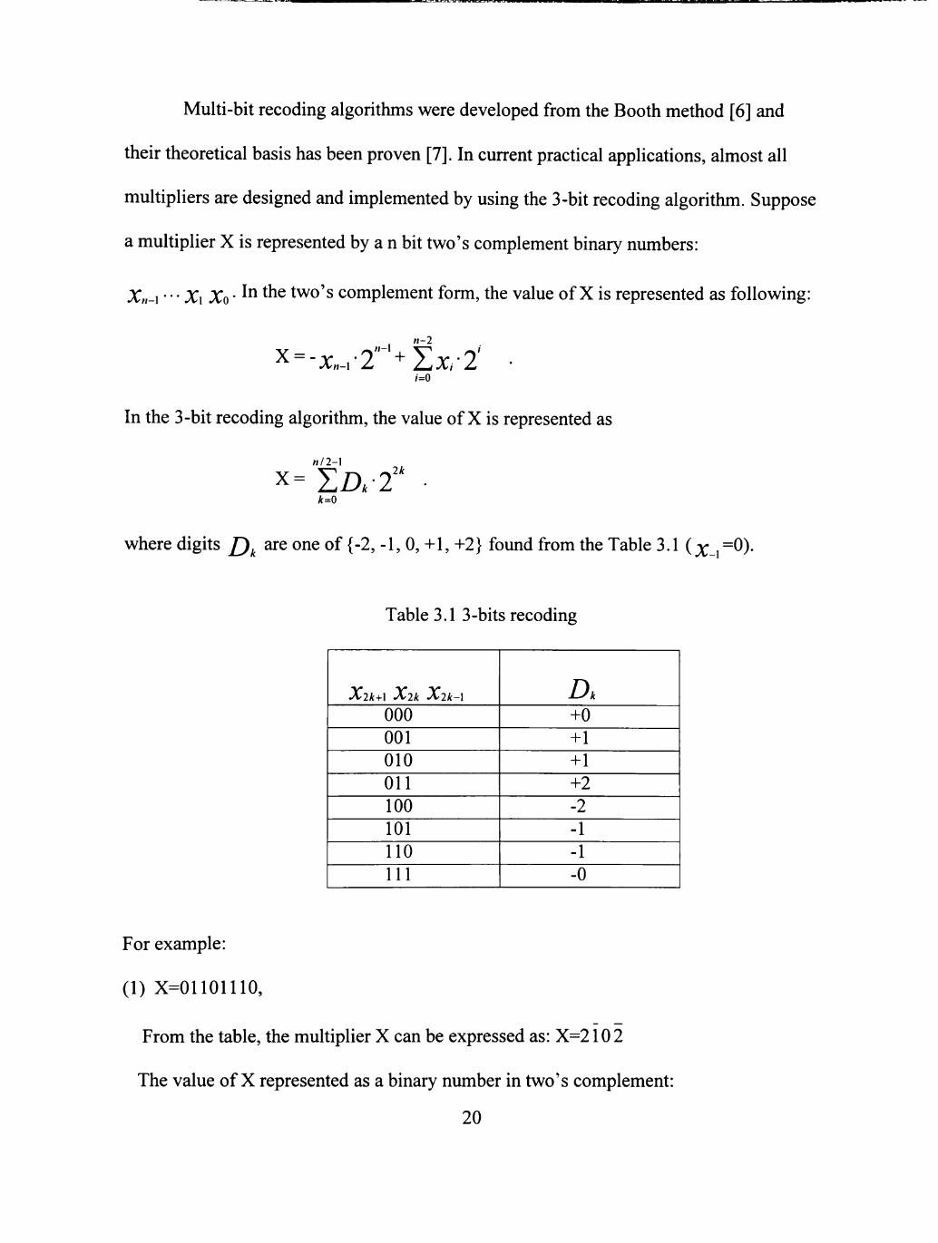
Multi-bit recoding algorithms were developed from the Booth method [6] and
their theoretical basis has been proven [7]. In current practical applications, almost all
muhipliers are designed and implemented by using the 3-bit recoding algorithm. Suppose
a multiplier X is represented by a n bit two's complement binary numbers:
X„-i • • • Xi Xo • ^^ ^^ two's complement form, the value of X is represented as following:
«-2
Jin-l Z /.u Xi ^ /=0
In the 3-bit recoding algorithm, the value of X is represented as
«/2-l
x= E A - 2 " A=0
where digits J)^ are one of {-2, -1, 0, +1, +2} found from the Table 3.1 (x_i=0)-
Table 3.1 3-bits recoding
X2A+I X2k X2k-\
000 001 010 on 100 101 no 111
Dk +0 +1 +1 +2 -2 -1 -1 -0
For example:
(1) X=01101110,
From the table, the multiplier X can be expressed as: X=2102
The value of X represented as a binary number in two's complement:
20

X = 2 ' + 2 ' + 2 ' + 2 ' + 2 '=110( inbase l0) .
The value of X represented with a number in radix 4 is given by
X = 2 x 2 ' - 2 ' - 2 = n0( inbasel0) .
(2) X=10010010,
X can be expressed as X = 2112 in radix 4.
The value of X represented with a binary number in two's complement:
X = - 2 ' + 2 ' + 2 ' =-110 (in base 10).
The value of X represented with a number in radix 4 is
X = -2x2 ' + 2 ' + 2 ' -2 = -110 (in base 10).
So, with the 3-bit recoding algorithm, a n bit two's complement binary number X
can be represented with half the number of symbols.
The multiplication, P, of X and Y can be written as
« / 2 - l M / 2 - 1 >2A. , , ^ V -r^ x^x ^2k p = xY = ( 2 A - 2 >Y = ( E A - ^ ) - 2
A=0 k=Q
So, the product P is the summation of only n/2 partial products (/)^ F)2 (k=0, ... n/2).
£)j^ e {0, 1, 2, -1, -2}, partial products can be easily obtained by shifting Y (or -Y). If
adder arrays are used, this kind of shifting is implemented with hard-wired connections.
The 3-bit recoding algorithm can be used in sequential and combinational, hardwire
and microprogrammed multipliers. The implementation of logic circuits for an 8 x 8 bit
parallel multiplier using the 3-bit recoding algorithm will be described in detail in the next
chapter.
21

CHAPTER IV
IMPLEMENTATION OF PARALLEL TWO'S COMPLEMENT MULTIPLIER
4.1 Architecture of an 8 x 8 bit Multiplier
Figure 4.1 shows the architecture of an 8 x 8-bit parallel multiplier using the 3-bit
recoding algorithm. The number of partial product rows is reduced to four. The two's
complement block is used to determine the two's complement of the multiplicand Y
which represents the negative of Y. The 3-bit Encoder gives four 4-bit codes: S ^ S ^
X[7:0]
V
Y[7:0]
3-bit Encoder
SA^'-0]\ [S, [3:0] LS,[3:0] Ls:3[3:0] V V V V V
b> Tvro's Complement
V -Y[7:0]
Partial Products selector
/J [8:0] V
/^[8:0]2 PJ8:0]2 V
/?[8:0]2' 11 V
Carry Save Adders Array
J Carry Select Adders
P[15:10] /
Rinnip C^i r ru A r l r l o r c n i U U I C V^ai 1 T rwjvik^u
P[9:4] V
22

Fig.4.1 Parallel multiplier of the 8 x 8-bit multiplier
5*3 and 5*4, which are used to determine p^. The Partial Products Selectors are four
identical multiplexers which are used to determine p^ (k=l ,2,3,4). The product P of X
and Y is:
P=P, ^ P2-2' ^ P.-2' ^ P.-2'
The partial products />, • 2' *' ^ ( ^=1' 2,3 and 4) are shifted 2(k-l) bits to the right
o^P^ and need be sign extended to 16 bits. Carry save adder arrays (CSA) are used to
add multiple inputs and change the summation of multiple numbers to the summation of
two numbers. There is no carry propagation delay in the carry save adders array. So, the
speed is high. Two 16 bits numbers A[15.. .0] and B[15...0] are obtained from the CSA.
The 4 least significant bits of B are zero, so, it is only needed to add the two numbers
A[15...4] and B[15...4]. For the least significant 4 bits, P[3...0]=A[3...0]. A Ripple
Carry Adder Array (RCA) is used to add A[9.. .4] and B[9.. .4] to obtain P[9.. .4]. A
Carry Select Adder Array is used to add A[15...10] and B[15...10] to obtain P[15...10].
The logic implementations of different multiplier blocks will be detailed in the
following section. These blocks are based on logic gates and half and full adder.
4.2. Two's Complement Block
The two's complement block is used to determine the two's complement
of the multiplicand Y which represents the negative of Y. Figure 4.2 shows the circuit of
the Two's complement block. According to the definition of two's complement, negative
23
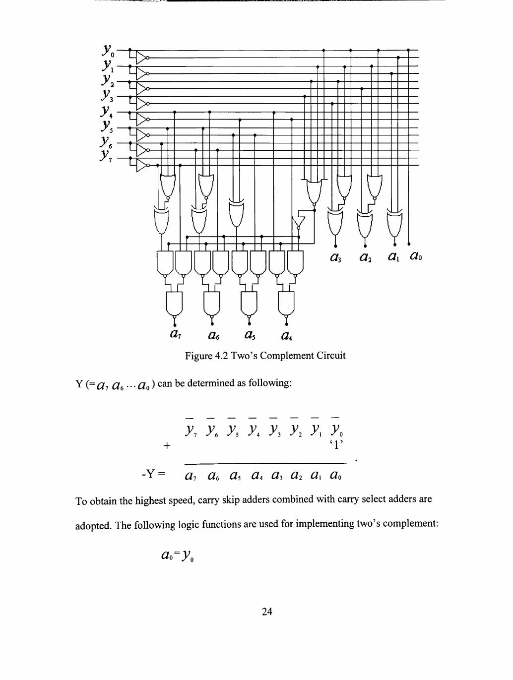
Qz a^ ai a^ vvw Y Y Y Y ^7 flffi at a^
Figure 4.2 Two's Complement Circuit
^ {^Gi Cl6-Clo) c^^ ^^ determined as following:
^7 ^6 ys yA -yI ^2 y\ y^ + '1'
-Y= ai Qe as UA as 2 a^ a^
To obtain the highest speed, carry skip adders combined with carry select adders are
adopted. The following logic functions are used for implementing two's complement:
ci^^y.
24

a,=y®y 1 -^ 0
The carry of the third bit is;
When C J = ' 0 ' .
Whenc3=' l ,
cr(y^^y2^y>^y«
a>=y,
a=y.
«'=X
a.-y,
ctA=y,
ary®y,
a.=yAy^^y^
a.=y®(y^^ys^y^ •
The third carry out Q^ is used to select which are upper four bits of-Y
25

4.2 3-bit Encoder Block
The 3-bit Encoder gives four words, ^^, g^, ^^ and 5*4, simultaneously based
on Table 4.1. ^^(k= 1,2,3,4) are used to determine p^. The following table shows how
to determine 5* and p^ by looking up three consecutive bits of the muhiplier X.
Table4.1 Encodes 5'J3...0]
X2k+\ X2k X2A-I
000 or 111
001 or 010
Oil
101 or 110
100
5J3...0]
0000
0001
0010
0100
1000
Pk
0
Y
2Y
-Y
-2Y
^ [3.. .0] are determined by using following logic functions:
Sk\.^^=hc2k.^+(x2k®X2kJ
Sk^^^=[x2k.X + ^2k'^X2kj
Sk^^^=^2k.. + ^2k®X2kJ
Sk\-^^=[X2k.l^X2k + X2k-l
26

Figure 4.3 shows the circuit for determining 5* [3...0]. There are four identical
circuits in the encoder block to determine 5* [3.. .0], ^'^ [3.. .0], ^3 [3.. .0] and
5 [3...0] in parallel.
X2it+1 -^^ifc Xsjfe-l - ^ 2 ^ 1 - ^ 2 * -^2^-1
V
• t • •
SJS] s,[2] S,U] S,[0]
Figure 4.3 Part of 3-bit encoder circuit
4.4 The Partial Products Selector
The circuit shown in Figure 4.4 is a basic circuit cell to build the partial
product select circuits. This basic cell is used to determine the i bit of the k partial
product (before shifting). In Figure 4.4, ^ j . , h^., ^3. and Jy^. are the i*" bits of Y, 2Y,
:th -th -Y and -2Y, and V is the i bit of the k partial product (before shifting 2k bits to the •^ ki
right).
27

11 11 n ^ \ / V V
Y
V
th Figure 4.4. Circuit to determine i bit of the k partial product
4.5 Carrv Save Adders Array Block
Figure 4.5 is a diagram of two carry save adders (CSA) arrays used to add four
binary numbers [1IJ. The carry save adder array, CSAl, is used to add three binary
numbers. There is no carry propagation on carry in. The carry of the i^ bit will be saved
as the value of C[i] and the sum of the i will be saved as the value of S[i]. The
A4[MSB:0]
A3[MSB:0]
A2[MSB:0]
A1 [MSB:0] CSAl
c> C1 [MSB:0]
S1 [MSB:0] CSA2
c> C2[MSB:0]
S2[MSB:0]
Figure 4.5 Carry save adders arrays
28

summation of three numbers: A1[MSB:0], A2[MSB:0] and A3[MSB:0] is equal to the
summation of two numbers: C[MSB:0] and S[MSB:0]. The carry save adders array,
CSA2, is used to add A4[MSB:0], C[MSB:0] and S[MSB:0]. So, the summation of four
numbers is transferred to the summation of two numbers quickly by using carry save
adders arrays with only a two-gate time delay.
4.6 Ripple Carrv Adders
Figure 4.6 shows 6-bit ripple carry adders consisted of 6 1-bit full adders.
A [9] B[9] A [5] B[5] A [4] B[4]
C[9] i
C[5] s
C[4] a b
s -C[3]
P[9] P[5] P[4]
Figure 4.6 Ripple carry adders
4.7 Carrv Select Adders
Figure 4.7 shows the carry select adders array. There are two identical 6-bit ripple
carry adder arrays. For one ripple carry adder array, the carry in is '0 ' ; for the other, the
carry in is ' 1'. Carry C[9] is used to determine which set of bits are the most significant 6
bits:P[15:10].
29

KTFzvc^zaa^^^i^^^vmM
A[15] B[15]
a b C, C,
i
^
Y P[15]
A[11] B[11] A[10] B[10]
a b C , C,
s
a b
C C, • ' 1 '
xyxv Y Y P[11] P[10]
C[9]
Figure 4.7 Carry select adders array
4.8 16 X 16 Bit Multiplier
A 16 X 16 bit multiplier can be implemented with 8 x 8 bit multiplier cells. Let
the multiplier X and multiplicand Y be represented with 16 bit signed binary numbers
in two's complement: X=x,, Xu ••• X, Xo ^ ^ Y= J ,5 > i4 •'• J i J^o"
The value of X and Y can be written as
x=(-o- 2' + S X, 2')+ X, • 2' +(- x,5 • 2' + 1 xs., 2') 2 ;=0
= X, + x,-2' + X.-2'
Y=(-o- 2' + 1 x 2 ' ) + 3^/2' +(->'„-2'+!>',„2')2 1=0 ;=0
30

= 7,+ X-2' + 7.-2'
The product of X and Y is then
^•Y=X,T,+(XT.+XaT,)2'+X.T.2"+z
z = (X, Y.+y, X)2 ' +(x,r. + y, X^)2" + x , x 2"-
So, four 8 X 8 bit multipliers are needed to obtain products of J^^ • y^, J^^ • Y2'
^ 2 • Yi ^^^ Jir2 • Y2 • Because the time delay for implementing the summation of Z in
the above function is shorter than the delay of the 8 x 8 bit multipliers, ripple carry adders
are used to determine Z. Figure 4.8 shows the adders array for implementing the
summation of X , T i ' ( X r ^2 + X 2 * T,) 2 ' ' X 2 ' Y2 T ^nd Z. The adders array
consists of carry save adders and carry select adder arrays.
Figure 4.8 Adders Array of 16 x 16 bit multiplier
31

CHAPTER V
LAYOUT OF CMOS MULTIPLIER INTEGRATED CIRCUITS
5.1 Overview of Integrated Circuits
An integrated circuit (IC) is an electronic network that has been fabricated on a
single piece of semiconductor material such as silicon [12]. The silicon surface is
subjected to various processing steps in which impurities and other material layers are
added with specific geometrical patterns. The steps are sequenced to form three
dimensional regions that act as transistors for use in switching and amplification. Passive
elements, such as resistors and capacitors, are not always intentionally included as
elements in the circuit, but often arise as parasitic elements due to the electrical properties
of the material. The "wiring" among the devices is achieved using interconnects, which
are patterned layers of low-resistance material such as aluminum. The resulting structure
is equivalent to creating a conventional electronic circuit using discrete components and
copper wires. So, an IC can be defined as a set of patterned layers. Each layer has specific
electrical characteristics, such as sheet resistance, and is patterned in accordance with the
layers above and below. Stacking different material patterns results in geometrical objects
that fiinction electrically as devices or interconnects.
A layout editor such as L-Edit is used to design the patterns on each layer and
accomplish the physical design of the chip
32

5.2 Design Philosophies
Digital VLSI can be implemented at several levels, depending upon the starting
point. The most common divisions are as follows:
1. Full Custom. In fiill custom design, every detail of the integrated circuit layout needs
to be completed. At this level, all gates must be designed, drawn, and simulated.
2. Cell Based. Cell based designs are based on interconnecting exiting cells stored in a
library, which is a collection of pre-designed gates and modules. The properties of
each cell, such as the speed and layout dimensions, are provided to the system
designer, who provides the arrangement and interconnect to implement the system.
Application-specific integrated circuits (ASICs) are usually constructed in this
manner.
3. Gate Arrays. Gate arrays consist of arrays of MOSFETs that can be wired using
interconnect lines to implement the desired fimctions. Logic circuits can be
prototyped very quickly using this approach.
The design and layout of the multiplier is performed at the gate level. First, the
standard primitive gates (NORs, NANDs, NOT, XOR and NXOR) are used to build
various blocks, such as 3-bit Encoder, two's complement of the multiplicand Y, partial
products selectors PI, P2, P3 and P4, carry save adder array 1 CSAl, carry save adder
array 2 CSA2 and carry select adder array. Second, the multiplier chip is implemented
by interconnecting these blocks.
33

5.3 The Floorplan
The floorplan of the chip shows the placement and area consumption of the major
logic fimctions in the finished chip. Floorplan design is performed at the architectural
level. All major operations groups are identified and the interconnect requirements are
studied. The placement of the cells is not arbitrary, since the large-scale system
performance is directly affected.
The floorplan is important to designers at all levels. At the system level, the
distance between functional blocks can limit the data transmission speed and, hence, the
performance of the chip. Circuit and cell design is often based on satisfying the electrical
specifications using the minimum amount of real estate consumption. Interconnect
routing affects every aspect of the design and operation of the network.
5.4 Interconnections
The limiting factor in high-density system design is the interconnect routing and
connections. One reason for this situation is the existence of basic layout rules such as
• The minimum width and spacing rules for wires on the same layer, and,
• Surround design rules that are required for contacts and vias.
These automatically limit the density of the wiring. Since each layer is intrinsically two-
dimensional, wires on the same layer cannot cross without creating an electrical short
circuit. Routing must be implemented using cross-overs and cross-unders, and the
problem can become very complex.
34

Interconnect routing is complicated by parasitic electrical coupling among lines
that are physically close to each other. This is termed as crosstalk, and can cause data
transmission errors.
Crosstalk problems can be difficult to isolate, particularly in high-density layouts.
It is therefore best to avoid it in the original design. The effects can be minimized by
obeying all design rule spacings, avoiding long lengths of parallel lines, and purposely
introducing "kinks" into the lines to disturb the coupling [12].
5.5 Floorplan and Phvsical Lavout of the Multiplier Chip
Figure 5.1 shows the floorplan and pins arrangements of the 8 x 8 bit multiplier
chip. To make the chip compact and interconnection short, partial products selectors: PI,
P2, P3, P4 and carry save adder array 1 are divided in the middle, so, interconnecfion can
go through these blocks. XO-7 is the 8 bits of the multiplier input. YO-7 is the 8 bits of the
multiplicand input. Vdd and Gnd are power supply and ground, respectively. P(0-15) is
the output of the multiplier.
Figure 5.2 shows the physical layout of the multiplier chip. The chip was
designed by using Tanner L-Edit CMOS layout tool with 1.2|im SCN (Scalable CMOS
N-well) technology. The chip area (not including padsframe) is 1mm .
35

YD
Y1
Y2
Y3
Y4
Y5
Y6
Y7
XO X1 X2 X3 Gnd X4 X5 X6
3-bit Encoder
P1 selector
P2 selector
P3 selector
P4 selector
Two's complement of Y
P1 selector
P2 selector
P3 selector
P4 selector
CSA1 CSA1
CSA
2
CSA2
Carry select adder array
Car
ry s
elec
t ad
der
arra
y
P (15) P(14) P(13) P(12] Vdd P(11) P(10) P(9)
X7
P(8)
P(0)
P(1)
P(2)
P(3)
P(4)
P(5)
P(6)
P(7)
Figure 5.1 Floorplan and pins arrangements of the multiplier chip
36

Figure 5.2 Physical layout of the chip
37

CHAPTER VI
PSPICE SIMULATION AND CHIP TEST
6.1 Pspice Simulation of Schematic Multiplier Circuit
Figure 6.1 shows a block diagram of the 8 x 8 multiplier.
DSTMJ
DSTlVtt JUML
X[7-0]
Y[7-0]
Hfil.
<Y[7-0] YC[7-0}.
ML
L XU-O] ;i[3-0]'
;2[3-D]
HB14
S1f3-D1
S2f3-D1
S3P-0) ??r3-t)i
S4[3-0} 5413-01
Y[7-D] ^S1[3-Ci]
S2P-0]
S3P-0]
S4[3-0]
YC[7-0]
YCP-D] PP1[8-D]
PP2[8-0]
PP3[S-D]
PP4[L=;-D]
P PI [8-0] Hfii .
PP2[8-0)
PP3[8-0]
PP4[8-0]
PP1[8-0]
PP2[8-0]
PP3[8-D]
PP4I8-D]
P[15-0]»
P[15-D]
_piia
111 IE IE _PI4]
li^ PI6
^ pp:
pp:
P[10
PM1
P[12
pri3 P[14]
P[15
y. <&
0
-J>&, 0
<8>
%
Figure 6.1 Schematic circuit of the 8 x 8 multiplier
For the 8 X 8 bit multiplier, there are 16 input pins assigned to the multiplier X
(=X7.. .Xo) and mulfiplicand Y (=Y7... Yo), and 16 output pins assigned to the product P
(=Pi5.. .Po). If a pin is at a high voltage level (5V), the corresponding bit is equal to
logical 1. If a pin is at a low voltage level (OV), the corresponding bit is equal to logical
0.
38

The multiplier was simulated first using a gate level Pspice simulation. The gates
were drawn from the Pspice library with default values of time delays. To verify the logic
function of the multiplier circuit, four different pairs of the multiplier and multiplicand
were used to check the outputs of the multiplier circuit.
For the 3-bit recoding algorithm implementation of the multiplier circuits,
if a multiplier X and multiplicand Y input voltage levels are applied to the multiplier,
generally speaking, the time delay of a higher bit of the product P is longer or equal to the
delay of a lower bit. From the discussion of Chapter IV, four partial products are selected
from 0, Y, 2Y, -Y and -2Y in parallel. By using carry save adder arrays CSAl and CSA2,
the summation of the four partial products is changed to the summation of two 16-bit
numbers A and B without carry propagation. A carry ripple adder array and a carry select
adder array are used to add A and B. So, for a higher order bit, if there is carry in, the
time delay of this bit will be longer than the delay of a lower bit. If there is no carry in,
the time delay can be equal to or less than that of a lower bit. It is apparent that the time
delays of output pins are dependent on the inputs X and Y. In the following pages, the
voltage level curves and the time delays of all output bins are discussed in detail for a
case with a multiplier of X=00001101 and a multiplicand of Y=00001001.
For a multiplier of X=00001 lOh (X= 13io) and a multiplicand of Y=0000100l2
(Y= 9io), the product P should be 00000000011 lOlOh (P= 117io). Figure 6.2 shows a
Pspice simulation result. A multipUer of X=00001 lOh and multiplicand Y^OOOOlOOh
are applied to the multiplier circuits at time t=0. From the plot, the product P is equal to
00000000011IOIOI2 after about 165ns delay.
39

When a multiplier of X and a multiplicand of Y are applied to the circuits. The
two's complement block and 3-bit encoder block are used to determine -Y and the
encoder words: ^^ (k=0, 1, 2, 3) simultaneously. From the implementation of-Y shown
in Figure 4.2, the time delay of a higher order bit of-Y is longer or equal to that of a
lower bit. The partial products: p^ (k=0, 1, 2, 3) are selected from Y and -Y based on the
word g^. In the case of a multiplier X=00001101 and a multiplicand Y=00001001, the
partial product PO is equal to Y with thesign extended to 16 bits. The partial product PI is
determined by shifting
P15 P14 P13 P12 P11 P10
P9 P8 P7 P6 P5 ?h P3 P2 P1 PO
OS 50ns 200ns 100ns 150ns Tine
Figure 6.2 Voltage levels of output P with X=00001 lOh and Y=0000100l2
250ns
-Y {=ai a, as a, a, ^2 a , ao) 2 bits to the right and with sign extended to 16 bits
(the most significant 7 bits of PI are the same and equal to QI )• The partial product P2 is
40

determined by shifting Y, 4 bits to the right and with the sign extended to 16 bits, and the
partial product P3 is equal to 0. The product P is equal to the summation shown in the
following:
/>(,= Y (sign extended): 0 0 0 0 0 0 0 0 0 0 0 0 1 0 0 1
P^ =-Y (shifted and sign extended): 1 1 1 1 1 1 1 1 1 1 0 1 1 1
/>2=Y (shifted and sign extended): 0 0 0 0 0 0 0 0 1 0 0 1
All bits oip^ have the same settling time as that of ^^ [0] because Y is selected with
5'o [0] to determine p^ . All bits of p ^ have the same settling time as that of ^'2 [0]
because Y is selected with ^^ [0] to determine p^. -Y is selected with ^^ [2] to
determine p^. Because there is no time delay for the least significant bit Q^ of-Y, the
time delay of the least significant bit of p^ is equal to that of ^^ [2]. The settling time of
a higher bit of p^ is longer or equal to that of a lower bit of p^. Because j ^ ^ =0, the
circuit for implementing ^^ [3.. .0] is simplified by removing the NXOR gate, so, the
time delay of SQ W (i=0, 2) is shorter than that of ^k P] ^^^^ 2, 3). From Figure 4.3,
the time delay of ^'i P] is longer than the one of 5', [0].
The least significant bit P[0] of the product P is equal to 1 with the same time
delay as that of ^ [0]. The bit P[l] is equal to 0 with no voltage level change because of
no carry in. The bit P[2] is equal to 1 with the same time delay as that of 5*, [2], so, the
time delay is longer than that of the bit P[0]. The bit P[3] is equal to 0 with no voltage
41

level change because of no carry in. Both bit P[4] and P[5] are equal to 1 and has the
same time delay for carry in from the previous bit, so, the time delay of P[4] and P[5] is
the same and longer than that of the bit P[2]. The bit P[6] is equal to 1 with a longer time
delay than that of bit P[5] because, for -Y, the time delay of the bit Q^ is longer than the
that of the bit Q^ (as shown in Figure 4.2). The bit P[7] is equal to 0 with no voltage
level change because of no carry in. For the bit P[8], after some time, the voltage level
will change from low to high, after a carry in, the voltage level will change from high to
low. The voltage level changes of bit P[9], P[10] and P[l 1] can not be seen from the plot,
because the time delay of the bit p^ [9] is longer than that of the bit p^ [8] and the
difference of time delays between p^ [9] and carry-in is less than the time step size. For
bits P[12], P[13], P[14], P[15], the voltage level change from low to high is at the same
time delay as p [9]. Because of the accumulative effects of the carry-in, the time delay
of the carry-in will increase from bit P[12] to P[15], so, the change of voltage level from
high to low will be later from bit P[12] to P[15].
Figures 6.3-6.5 shows a Pspice simulation result for the 8 x 8 bit multiplier with
the other three pairs of the multipliers and multiplicands: X=l 111001 h and
Y=0000100l2,X=1111001l2andY=1111011l2,X=0000110l2andY=1111011l2,
corresponding multiplications should be P=l 11111111000101 h (= -117io),
P=000000000111010l2(=117io),P=111111111000101l2(=-117io).
42

P15 P1i» P13 P12 P11 P10
P9 P8 P7 P6 P5 PU P3 P2 PI PO
r" i ~
1
1
1 1
1 1 1
1
1 1 —
Os 50ns 200ns 100ns 15ens Tine
Figure 6.3 Voltage levels of output P with X=l 11100112 and Y=0000100l2
250ns
P15 P14 P13 P12 P11 P10
P9 P8 P7 P6 P5 Ph P3 P2 PI PO
Os 50ns 200ns 100ns 150ns Tine
Figure 6.4 Voltage levels of output P with X=l 111001 h and Y=l 111011 h
250ns
43

P15 P1U P13 P12 P11 P10
P9 P8 P7 P6 P5 Pi» P3 P2 PI PO
Os 50ns 200ns 100ns 150ns Tine
Figure 6.5 Voltage levels of output P with X=0000101 h and Y=l 111011 h
250ns
The voltage level change and time delay for different bits of the product can be
explained in the same way. After a delay of about 150ns, the product P is equal to
1111111110001011,0000000001110101 and 1111111110001011, respectively.
For the 16 X 16 bit muhiplier, there are 32 input pins for the multiplier X
bits: Xi5.. .Xo and the multiplicand bits: Y15... Yo, and 32 output pins for the
multiplication P bits: P31.. .Po-
The following figures show Pspice simulation results. PL15...PL0 and
PM15.. .PMo are the least significant 16 and the most significant 16 bits of the product P.
Inputs X and Y are applied at time t=0 (not shown in figures).
44
LL

PM15 PM1i» PM13 PM12 PM11 PM10 PM9 PM8 PM7 PM6 PM5 PMI» PM3 PM2 PM1 PMO
PL15 PL14 PL13 PL12 PL11 PL10 PL9 PL8 PL7 PL6 PL5 PLi» PL3 PL2 PL1 PLO
Os 100ns 2 00ns 3 00ns 400ns 50ens Time
Figure 6.6 Output P with X=0000000000001101 and Y=0000000000001001
Figure 6.6 shows a Pspice simulation result for the 16 x 16 bit multiplier with a
multiplier of X=0000000000001 lOh (X=13io) and a multipUcand of Y
=00000000000010012 (Y=9io), the product is P= 00 ... OOlllOlOh
(P=117,o)
Figure 6.7 shows a Pspice simulation resuU for the 16 x 16 bit multiplier with a
multiplier of X=l 11111111111001 h (X=-13io) and a multiplicand of Y
=00000000000010012 (Y=9io), the product is P= \1 ... 1/000101 h
(P=-117,o)
45

PM15 PM1l» PM13 PM12 PM11 PM10 PM9 PN8 PM7 PM6 PM5 PM4 PM3 PM2 PM1 PMO
PL15 PL1U PL13 PL12 PL11 PL18 PL9 PL8 PL7 PL6 PL5 PLi» PL3 PL2 PL1 PLO
Os
1
1 1 1
1 1 1 1 1
1 1 1 1 1
1 1 1
1 1 1 1 1 1
1 1 1
1
1 1 1 1 1
_ l
1 1
1 1 1
1 1 1 1 1 1
1 1 1
1 1
1 1
lOOns UOOns
Fi
200ns 300ns Time
gure 6.7 Output P with X=l 111111111110011 and Y=0000000000001001
500ns
Figure 6.8 shows a Pspice simulation result for the 16 x 16 bit multiplier with a
multiplier of X=l 11111111111001 h (X= -13io) and a multiplicand of Y
=11111111111101112 (Y=-9io), the productionisP= 00 ... OOIIIOIOI2
(P=117io) 29
46
Im s ^ / i j

PM15 PM1U PM13 PM12 PM11 PH10
PM9 pri8 PM7 PM6 PM5 PMl» PM3 PM2 PM1 PMO
PL15 PL1U PL13 PL12 PL11 PL10
PL9 PL8 PL7 PL6 PL5 PL«* PL3 PL2 PL1 PLO
Os
L 1 1 1 1 1 1 1 1 1 1 i 1
1 1
1
1 1 1—1 r
1 1
1 1
1 1
1
1 1 1 1
1 1 1
1
1 1
1 1—1 1—1
1 1 1—1 1—1 n
I I I I I I I I I 1 1 1 1 1
1 ~i
1 1 1 1 1 1
100ns UOOns
Fi
200ns 300ns Time
gure 6.8 Output P wi thX=l ln i l 1111110011 and Y=ll 11111111110111
500ns
Figure 6.9 shows a Pspice simulation result for the 16 x 16 bit multiplier with a
multiplier of X=0000000000001 lOh (X= 13io) and a multiplicand of Y
=11111111111101 ll2(Y=-9io), the product is P= 11 ... 11000101 h
(P=-117io)
47
L

PM15 PM1i» PM13 PM12 PM11 PM10 PM9 PMO PM7 PM6 PM5 PMU PM3 PM2 PM1 PMO PL15 PL1I» PL13 PL12 PL11 PL10 PL9 PLO PL7 PL6 PL5 PLU PL3 PL2 PL1 PLO
1 1 1 1
1 r
1
1 1 1 1
1 1 1 1
1 1
1 1 1
1 1 1
1 1 1 1 1
1 1
1 1
1 1 1 1
1 1 i_ i 1
1
1
1
1 1 1 1
Os 100ns 200ns 300ns UOOns 500ns Time
Figure 6.9 Output P with X=0000000000001101 and Y=l 111111111110111
From the plots, all bits of the products P are settled and valid at about 240ns after
inputs X and Y are applied to thel6 x 16 bit multiplier.
6.2 Discussions of Pspice Simulation Results
From these simulations, it is clear that both the 8 x 8 bit multiplier and the 16 x
16 bit muhiplier works. The time delay of the 8 x 8 bit muhiplier is about 165ns and the
time delay of the 16 x 16 bit multiplier is about 240ns. So, the time delay of the 16 x 16
bit muhiplier is about 1.5 times that of the 8 x 8 bit multiplier.
48

6.3 Post Lavout Simulation Results
After verifying the multiplier circuits, the layout of the circuit was completed.
L-Edit IC layout tool was used for the layout of the 8 x 8 bit multiplier chip.
The layout of the entire 8 x 8 bit multiplier chip (including pads frame) has been
extracted and simulated at the transistor level using the Pspice simulation tool and de\ ice
parameters.
Figure 6.10 shows a post layout Pspice simulation result of the 8 x 8 bit multiplier
chip with a multiplier of X=00001 lOh (X= 13io) and multiplicand of Y=0000100l2 (Y=
9io) applied to the multiplier chip at time t=0. From the simulation, the product is
P=00000000011IOIOI2 (P= 117io). Comparing Figure 6.10 and Figure 6.2, we see large
differences in the time delays and voltage level waves of the output bits. This is because
the time delays of the standard gates from Pspice library are much longer than those of
gate cells from the L-Edit library, and the differences of the time delay of different gates
are large.
Figure 6.11-6.13 shows the Pspice simulation results for the 8 x 8 bit multiplier
with the other three pairs of the muhipliers and muhiplicands: X=l 11100112 and
Y=0000100l2,X=1111001l2andY=1111011l2,X=0000110l2andY=1111011l2. The
corresponding product is P=l 1111111100010112 (= -117io),
P=000000000111010l2(=117io), and P=l 11111111000101 l2(=-117io), respectively.
From these simulations, the time delay of the chip is about 5.5ns.
49

6.0U-r-
^ \
eu
6.0U
t PO PI
I U(Po_0) » U(P0_1)
/
lU/ :\ J-. \ .
ou
6.eu
t P2 f
n U(Po_2) <f U(Po_3)
ou
T P4 P5
6.0U-r-a U(PO_J|) « U(P0_5)
S E L » ! U\. 0U+ r r-
Os 1ns 2ns o U(Po 6 ) <• U(Po 7)
t P6 T
__,— <tns
— I —
5ns
Tine
_ _ i —
6ns
_ _ i —
7ns
_ _ i —
9ns Sns 8ns lens
6.0U
OU
6.0U
r 1 ._--'"
t t
1
X'--W Lv..
P8
1 P9 • 1
i : • •
D U(Po_8) o U(Po_9)
1 1
I 1 s J ; \
PIO
i P l l • !
i : i a U(PO_10) V U(P0_11)
6.0U-r-
. r S E L » ^ - ~ - _ V
ou
6.0U
v_
P12
D U(Po_12) » U(Po_13)
L • ,/' \ •
P14 P15 •
I : i 0U+ r r r-
Os 1ns 2ns Sns a U(Po_1i») o U(Po_15)
-I 9ns lOns iins 5ns
Tine
6ns 7ns Sns
Figure 6.10 The output P=00000000011IOIOI2
50
Lw

6.0U-r-
i V \
/ / ^
..^ OU
6.0U-r
T PO
T PI
OU
6.0U-T-
u U(Po_0) o U(Po_1)
1
f f P3
OU
6.0U
S E L »
u U(Po_U) » U(Po_5)
D U(Po_2) < U(Po_3)
1
{ I : : : 1
P4 i
P5
1
\ / P6
A
T P7
0U + r r r r-Os Ins 2ns Sns 4ns
o U(Po_6) * U(Po_7) 9ns
1 10ns
— I —
Sns
Tine
6ns _ _ i —
7ns
_ _ i —
Sns
6.0U
/
OU
t P8
t P9
U(Po_8) 0 U(Po_9) 6.0U-.--
eu
l\. I ' I
t PIO Pl l
U(Po_10) o U(Po_11) 6.0U-r-
I I
/ 1\ I
OU
t : I P12 • P13
U(Po_12) * U(Po_13) 6.0U-r
/
1\ S E L » |
0 U + -Os
J t
PH t
P15
-I , , r--
I ns 2ns Sns U(Po_1ii) • U(Po_15)
Uns 5ns
Time
6ns 7ns Sns 9ns lOns
Figure 6.11 The output P=l 11111111000101 h
51
1 u

1
1 -' ^ iS - / 1 v^ \ • /
t PO T
a U(PO_0) » U(P0_1)
1
\ 1
t P2 ?
o U(Po_2) < U(Po_3)
1
1 r ; 1
t P4
t P5
u U(Po_l») * U(P0_5)
1
J E L » ;
Os 1ns 2ns B U(Po_6) <. U(Po_7)
3ns
• X '•'
itns 5ns 6ns
1 P6
7ns
? Sns 9ns 10ns
Time
6.0U-r . . ^ ^
i / i '"•
P8 P.9
U : T • 1 a U(Po_8) * U(Po_9)
6.0U-r
QfJJ.
D U(Po_10) ^ U(Po_11) 6.0U-r
\ PIO P l l
V , ^ I ^ I
! \ • / \ • • P12 P13
Oyj. a U(P0_12) o U(P0_13)
6.0U-r
k J \ P14 • P15
V . 1 : i
Time a U(Po_1i») * U(Po_15)
Figure 6.12 The output P=00000000011 lOlOh
52
OUH 1 1 1 ' ' 1 1 1 ' 1
Os Ins 2ns Sns Uns 5ns 6ns 7ns Sns 9ns 10ns

6.0U
• /
r~
\<.\ // o.ou
6.0U-r
ou
6.0U-r
OU
6.0U-r-a U(Po_4) « U(Po_5)
t PO
r PI
a U(PO_0) <> u(Po_l)
1
1 : ? ;
t : P3 •
D U(Po_2) < U(Po_S)
1 1 y^ '
t
v. . \
\ V, r i T : 1
/: f^'
SEL»1 0U+-
P6 1..,
1 P7
Os Ins 2ns n U(Po 6 ) -. U(Po 7)
Sns 4ns 5ns
Time
6ns 7ns Sns 9ns 10ns
6.eu
S E L » OU
1 .„ 1
1
: : : t P8
1 : i P9 •
£1 U(Po_S) » U(Po_9) 6.0U-r-
1\ O.OU
PIO f
P l l
o U(Po_10) <; U(Po_11) 6.0U-r-
r iV
ou
6.0U
t P12
f P13
U(P0_12) » U(P0_1S)
v . ^ ;
r /
.V
! •
PH • t i
P15 !
OU-f r r r-Os Ins 2ns Sns
ci U(Po_1ii) * U(Po_15) 4ns 5ns
Tine
6ns 7ns Sns 9ns 10ns
Figure 6.13 The output P=l 11111111000101 h
53

6.4 Chip Test Resuhs
The 8 X 8 bit multiplier chip has been fabricated and tested. Figure 6.14 shows the
test setup. A fiinction generator was used to generate a square wave with a low voltage
level equal to OV and high voltage level equal to 5V. There are 16 input pins to the chip
among which 8 input pins are for a multiplier X (=X7.. .XIXO) input and the other 8 pins
for a multiplicand Y (=Y7... Yl YO) input. During the test, some pins of X and Y were
connected to the output of the function generator and all other pins were connected to the
ground. For example, in the case of testing the output of the chip with a multiplier X
(=00001IOI2) and multiplicand Y (=000010012), pins X3, X2, XO, Y3 and YO were
connected to the output of the ftinction generator and all other pins were connected to
ground. A logic analyzer, which can test 32 channels simultaneously.
2
g
VGnd Figure 6.14 Chip Test Configuration
54

was used to record the voltage waves of the multiplier X, multiplicand Y and product P.
To determine the time delay, points with mid voltage level on input and output curves
were chosen. So, a threshold with value of 2.5V was chosen during the test.
Figures 6.15 and 6.16 shows input and output voltage level curves of the chip.
From the plot, X=00001 IOI2 and Y=0000100l2 were applied to the chip at time t=0, and
after 20ns, the output was settled with P=00000000011IOIOI2.
To test the output of the chip with a multiplier X (=111100112) and muhiplicand
Y (=000010012), the pins of X7, X6, X5, X4, Yl, XO, Y3 and YO were connected to the
output of the fimction generator and all other pins were connected to ground.
Figures 6.17 and 6.18 shows input and output voltage level curves of the chip.
From the plot, X=l 11100112 and Y=0000100l2 were applied to the chip at time t=0, after
20ns, the output was settled with P=l 11111111000101 h.
Because the time resolution of the logic analyzer is 10ns, the total time delay of
the chip is less than 20ns. From the document provided by the Mosis company [13], the
time delay of the pads is 14.3ns, so the time delay of the multiplier circuit itself is less
than 5.7ns.
55

* ! *
Figure 6.15 Inputs XI and Yl of the chip
56

ilACHINE 1
ilarkers
Accumulate
^ime/Div
- Timing ifevefonfis
Time x to Trio
Off 0 to Triq
10 ns Delau
20 ns
20 ns
0 s
Time X to 0 0 s
At X darker P
0000
p L P P P P
E
jOyj 01 02
i3|
a 3 M
m 1
t
ill
E E
13 a 33 15
•4-
Figure 6.16 Output of the chip with inputs XI and Yl
57

*
flarkers
Accuntulste
Tiine/Div
Time
X
X X
E J J - Tilling Havefonos
X to Tr ig
0 to Tr ig
Delay
Off
10 ns
0 s Time X to 0 0 s
0 s At X Marker X
0 s F3
E X Oil
M M
X X X X
B m B 53 M m 02 f^Tf
ijJil
I iSl
IJtt
071
Figure 6.17 Inputs X2 and Y2 of the chip
58

*
MACHINE 1
Markers
Accumulate
Time/Div
P 001 P 01 P 02 P 031 P 04 P 051 P 061 P 071 p oa P 091 p ia p 111 P 12 F 131 P M P 13
-
- Timing Havefonos
Time | x to Trio
|Off |0 to Triq
10 ns 1 Delay
1 1 1
__
20 ns
20 ns
0 3
! 1
Time X to 0
At X Marker
0 s
P
FF8B
1 1 1
1 1
1
1
; :
1 :
= 1 ; (
1
= 1 i 1
1
1 ' ' 1 1
i J ! 1
Figure 6.18 Output of the chip with input X2 and Y2
59

6.5 Compare of Post-Lavout Simulation and Chip Test Results
From the post-layout simulations, the time delay of the 8 x 8 bit multiplier is
about 5.5ns. From the chip tests, the time delay of the 8 x 8 bit muhiplier chip is greater
than 10ns and less or equal to 20ns. The difference is attributed to the following two
reasons:
1. L-Edit' pads frame were used for post-layout simulation and Mosis company's pads
frame was used for fabrication.
2. Parasitic capacitors have not been included in the extracted circuits.
60

CHAPTER VII
CONCLUSIONS
Among all algorithms for multiplication, multibit recoding algorithms are the
most dominant in recent applications of multiplier designs and implementations. The
newly proposed 5-bit recoding algorithm [9] can compress a larger number of partial
product rows. It may be feasible for higher bit muhipliers (e.g., a 32 x 32 bit multiplier),
but it is not good for our 8 x 8 bh multiplier building block because of the complicated
circuits needed for implementing odd multiples of the multiplicand. The 3-bit recoding
algorithm is used in this work to design and implement an 8 x 8 bit multiplier that can
be used as an ASIC building block.
Two factors determine the performance of the multiplier chip. One is the
architecture of the multiplier and the other is the floorplan and interconnection of the
multiplier circuits. To obtain the highest speed, (1) carry skip adders combined with carry
select adders are used to implement the two's complement of a multiplier X, and (2) carry
save adders combined with carry select adders are used to add the partial products. To
reduce signal propagation delay, an effort has been made to make the floorplan and
interconnection of the multiplier circuits as compact and simple as possible.
The 8 X 8 bit multiplier chip has been designed and implemented physically with
1.2|j.m CMOS SCN technology by using the Tanner L-Edit CMOS layout tool. The area
of the circuits (not including the pads frame) is 1 mm^.
The chip has been fabricated and tested by using a function generator and a logic
analyzer with a resolution of 10ns. The total time delay of the chip is less than 20ns, and
61

the time delay of the multiplier itself (not including the pads delay) is less than 5.7ns.
A 16 X 16 multiplier implemented with 8 x 8 multiplier cells has been also
presented. From the simulation, the time delay of the 16 x 16 multiplier is about 1.5 times
that of the 8 x 8 multiplier. So, the time delay is about 8.6ns. A recent 16x16 multiplier
using 3-bit recoding in 0.9 ^m CMOS has a delay of 25ns and an area of 0.73 mm [9].
So, we designed and implemented a high speed multiplier building block.
Combined with other building blocks such as ALU, Control Unit, Adders, Multiplexers,
Register file. Accumulator, any kind of processor can be implemented.
The design and implementation of the multiplier building block was based at gate
level. If the design and implementation is at transistor level, the execution time of the
multiplier building block can be much faster.
62

REFERENCES
1. Glenford J. Myers, Digital System Design With LSI Bit-Slice Logic, 1979, John Wiley & Sons, New York.
2. Vijay K. Madisetti, Vlsi Digital Signal Processors, Butterworth-Heinemann, 1990, Boston, MA.
3. R. Townsend, Digital Computer Structure and Design, Newnes-Butterworths, 1992, London.
4. Milos D. Ercegovac," Fast Multiplication Without Carry-Propagate Addition," IEEE Trans. Comput.,pp. 1385-1390, Vol. 39, No. 11, Nov. 1990.
5. Zhi-Jian, "Overtumed-Stairs" Adder Trees and Multiplier Design," IEEE Trans. Comput., pp. 940-948, Vol. 41, No. 8, August 1992.
6. L. Dadda, "Some schemes for parallel multipliers," Alta Frequenza, vol. 34, pp. 349-356, Mar. 1965.
7. A. D. Booth, "A signed binary multiplication technique," Quarterly J. Mechan. Appl. Math., Vol. IV, part 2, 1951.
8. Stamatis Vassiliadis, "A General Proof for Overlapped Multiple-Bit Scanning Multiplications," IEEE Trans. Comput., pp. 172-183, VOL. 38, NO. 2, Feb. 1989.
9. Homayoon Sam, "A Generalized Multibit Recoding of Two's Complement Binary Numbers and Its Proof with Application in Multiplier Implementations," IEEE Trans. Comput., pp. 173-183, Vol. 39, No. 8, August. 1990.
10. Vincent P. Heuring, Computer Systems Design and Architecture, 1997, Addison-Wesley, Menlo Park, California.
11. Michael John Sebastian Smith, Application-Specific Integrated Circuits, 1997, Addison-Wesley, Menlo Park, California.
12. John P. Uyemura, Physical Design of CMOS Integrated Circuits Using L-Edit, 1998, PWS Publishing Company, Boston, Massachusetts.
13. Document for mosis pads from http://www.mosis.com/~dsp21a.tmp
63

•I' TMniii v'l -Tifc ^iaBS
PERMISSION TO COPY
In presenting this thesis in partial fulfillment of the requirements for a
master's degree at Texas Tech University or Texas Tech University Health Sciences
Center, I agree that the Library and my major department shall make it freely
available for research purposes. Permission to copy this thesis for scholarly
purposes may be granted by the Director of the Library or my major professor.
It is understood that any copying or publication of this thesis for financial gain
shall not be allowed without my further written permission and that any user
may be liable for copyright infringement.
Agree (Permission is granted.)
Student's Signature Date
Disagree (Permission is not granted.)
Student's Signature Date