Embed Size (px)
Citation preview
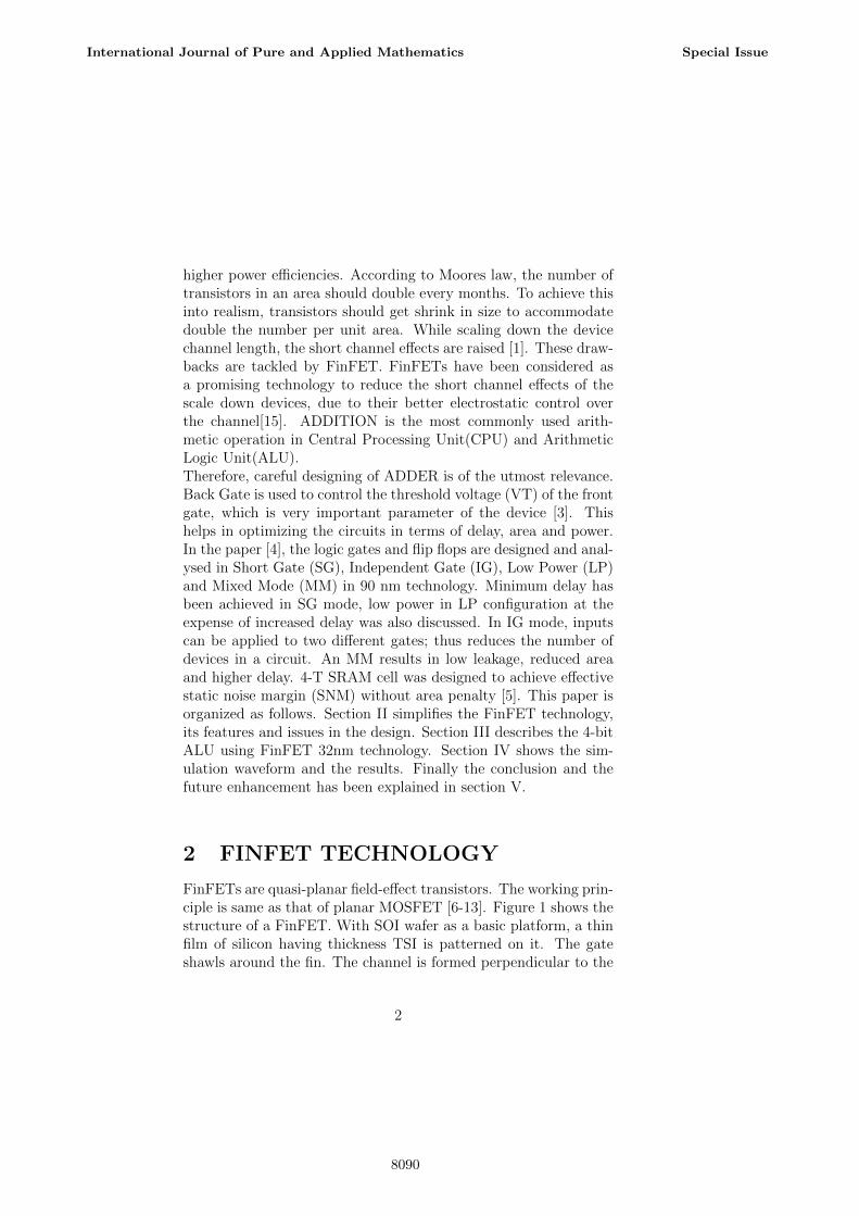
Design of Low power 4 bit ALU using 32nm FinFET technology
Jency Rubia J1, Babitha Lincy R2,1,2Department of ECE,
3Sri Venkateswara College of Engineering,Chennai,India.
[email protected]@gmail.com
July 19, 2018
Abstract
This paper proposes a 4-Bit Arithmetic logic unit (ALU)using FinFET at 32nm technology. The CMOS has beenused widely in current technology. But scaling the CMOSwill cause the short channel effects such as DIBL, GIDL, Subthreshold swing, channel length modulation, mobility degra-dation etc. To change nanoscale CMOS, a multi gate devicecalled FinFET is suggested. FinFET has its own advantagesover the CMOS such as reduction in leakage power, operat-ing power, leakage current and transistor gate delay, reducedthreshold level and steeper subthreshold swing. The targetof this paper is to reduce and calculate leakage power of4-Bit ALU using FinFET.
Key Words:FinFET technology; Cmos technology; Arith-metic logic unit (ALU); Leakage power; Low power analysis;Delay analysis.
1 INTRODUCTION
Today mobile and computing markets continue to innovate at a dra-matic rate delivering more performance in smaller form factors with
1
International Journal of Pure and Applied MathematicsVolume 120 No. 6 2018, 8089-8100ISSN: 1314-3395 (on-line version)url: http://www.acadpubl.eu/hub/Special Issue http://www.acadpubl.eu/hub/
8089
higher power efficiencies. According to Moores law, the number oftransistors in an area should double every months. To achieve thisinto realism, transistors should get shrink in size to accommodatedouble the number per unit area. While scaling down the devicechannel length, the short channel effects are raised [1]. These draw-backs are tackled by FinFET. FinFETs have been considered asa promising technology to reduce the short channel effects of thescale down devices, due to their better electrostatic control overthe channel[15]. ADDITION is the most commonly used arith-metic operation in Central Processing Unit(CPU) and ArithmeticLogic Unit(ALU).Therefore, careful designing of ADDER is of the utmost relevance.Back Gate is used to control the threshold voltage (VT) of the frontgate, which is very important parameter of the device [3]. Thishelps in optimizing the circuits in terms of delay, area and power.In the paper [4], the logic gates and flip flops are designed and anal-ysed in Short Gate (SG), Independent Gate (IG), Low Power (LP)and Mixed Mode (MM) in 90 nm technology. Minimum delay hasbeen achieved in SG mode, low power in LP configuration at theexpense of increased delay was also discussed. In IG mode, inputscan be applied to two different gates; thus reduces the number ofdevices in a circuit. An MM results in low leakage, reduced areaand higher delay. 4-T SRAM cell was designed to achieve effectivestatic noise margin (SNM) without area penalty [5]. This paper isorganized as follows. Section II simplifies the FinFET technology,its features and issues in the design. Section III describes the 4-bitALU using FinFET 32nm technology. Section IV shows the sim-ulation waveform and the results. Finally the conclusion and thefuture enhancement has been explained in section V.
2 FINFET TECHNOLOGY
FinFETs are quasi-planar field-effect transistors. The working prin-ciple is same as that of planar MOSFET [6-13]. Figure 1 shows thestructure of a FinFET. With SOI wafer as a basic platform, a thinfilm of silicon having thickness TSI is patterned on it. The gateshawls around the fin. The channel is formed perpendicular to the
2
International Journal of Pure and Applied Mathematics Special Issue
8090
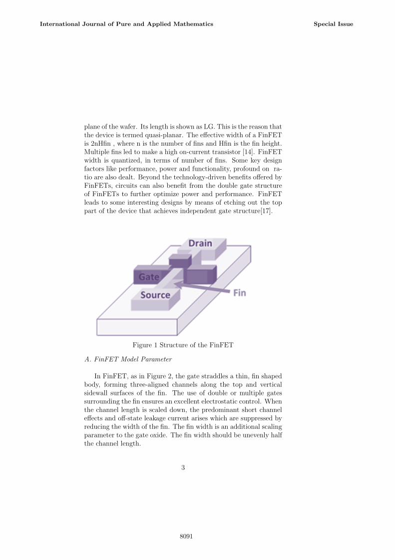
plane of the wafer. Its length is shown as LG. This is the reason thatthe device is termed quasi-planar. The effective width of a FinFETis 2nHfin , where n is the number of fins and Hfin is the fin height.Multiple fins led to make a high on-current transistor [14]. FinFETwidth is quantized, in terms of number of fins. Some key designfactors like performance, power and functionality, profound on ra-tio are also dealt. Beyond the technology-driven benefits offered byFinFETs, circuits can also benefit from the double gate structureof FinFETs to further optimize power and performance. FinFETleads to some interesting designs by means of etching out the toppart of the device that achieves independent gate structure[17].
Figure 1 Structure of the FinFET
A. FinFET Model Parameter
In FinFET, as in Figure 2, the gate straddles a thin, fin shapedbody, forming three-aligned channels along the top and verticalsidewall surfaces of the fin. The use of double or multiple gatessurrounding the fin ensures an excellent electrostatic control. Whenthe channel length is scaled down, the predominant short channeleffects and off-state leakage current arises which are suppressed byreducing the width of the fin. The fin width is an additional scalingparameter to the gate oxide. The fin width should be unevenly halfthe channel length.
3
International Journal of Pure and Applied Mathematics Special Issue
8091
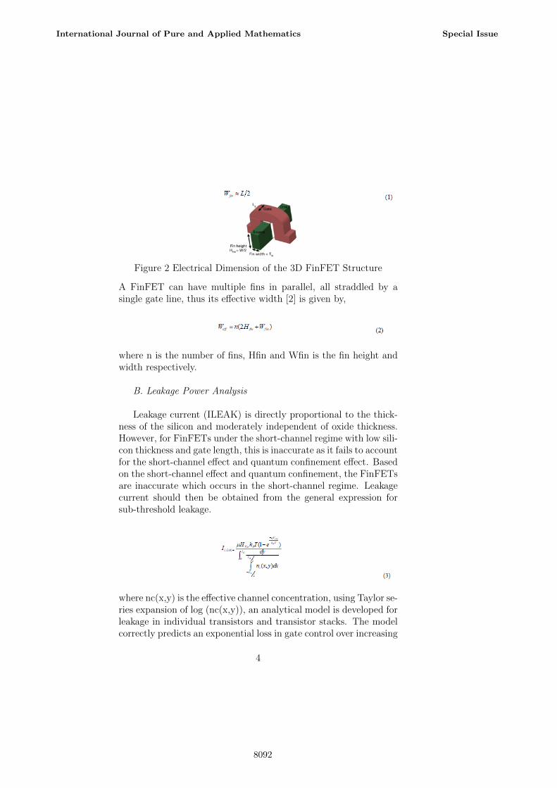
Figure 2 Electrical Dimension of the 3D FinFET Structure
A FinFET can have multiple fins in parallel, all straddled by asingle gate line, thus its effective width [2] is given by,
where n is the number of fins, Hfin and Wfin is the fin height andwidth respectively.
B. Leakage Power Analysis
Leakage current (ILEAK) is directly proportional to the thick-ness of the silicon and moderately independent of oxide thickness.However, for FinFETs under the short-channel regime with low sili-con thickness and gate length, this is inaccurate as it fails to accountfor the short-channel effect and quantum confinement effect. Basedon the short-channel effect and quantum confinement, the FinFETsare inaccurate which occurs in the short-channel regime. Leakagecurrent should then be obtained from the general expression forsub-threshold leakage.
where nc(x,y) is the effective channel concentration, using Taylor se-ries expansion of log (nc(x,y)), an analytical model is developed forleakage in individual transistors and transistor stacks. The modelcorrectly predicts an exponential loss in gate control over increasing
4
International Journal of Pure and Applied Mathematics Special Issue
8092
silicon thickness or decreasing gate length, and hence an exponen-tial increase in ILEAK. From the above remarks, we formulate amacro model for leakage in SG-mode FinFET as
where a1,a2,b1 are the coefficients.
C. Challenges in FinFET
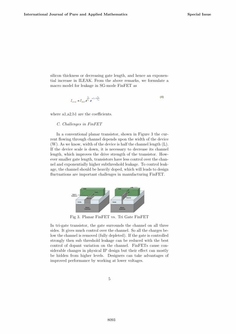
In a conventional planar transistor, shown in Figure 3 the cur-rent flowing through channel depends upon the width of the device(W). As we know, width of the device is half the channel length (L).If the device scale is down, it is necessary to decrease its channellength, which improves the drive strength of the transistor. How-ever smaller gate length, transistors have less control over the chan-nel and exponentially higher subthreshold leakage. To control leak-age, the channel should be heavily doped, which will leads to designfluctuations are important challenges in manufacturing FinFET.
Fig 3. Planar FinFET vs. Tri Gate FinFET
In tri-gate transistor, the gate surrounds the channel on all threesides. It gives much control over the channel. So all the charges be-low the channel is removed (fully depleted). If the gate is controlledstrongly then sub threshold leakage can be reduced with the bestcontrol of dopant variation on the channel. FinFETs cause con-siderable changes in physical IP design but their effect can mostlybe hidden from higher levels. Designers can take advantages ofimproved performance by working at lower voltages.
5
International Journal of Pure and Applied Mathematics Special Issue
8093
3 4 BIT ALU USING FINFET
A. Overview of ALU
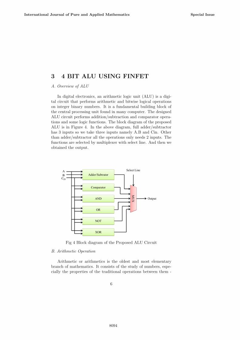
In digital electronics, an arithmetic logic unit (ALU) is a digi-tal circuit that performs arithmetic and bitwise logical operationson integer binary numbers. It is a fundamental building block ofthe central processing unit found in many computer. The designedALU circuit performs addition/subtraction and comparator opera-tions and some logic functions. The block diagram of the proposedALU is in Figure 4. In the above diagram, full adder/subtractorhas 3 inputs so we take three inputs namely A.B and Cin. Otherthan adder/subtractor all the operations only needs 2 inputs. Thefunctions are selected by multiplexer with select line. And then weobtained the output.
Fig 4 Block diagram of the Proposed ALU Circuit
B. Arithmetic Operation
Arithmetic or arithmetics is the oldest and most elementarybranch of mathematics. It consists of the study of numbers, espe-cially the properties of the traditional operations between them -
6
International Journal of Pure and Applied Mathematics Special Issue
8094

addition, subtraction, multiplication and division. Arithmetic is anelementary part of number theory, and number theory is consideredto be one of the top-level divisions of modern mathematics, alongwith algebra, geometry and analysis. The designed arithmetic logicunit does the arithmetic operations of addition, subtraction andcomparison operations. The comparator consists of lesser, greaterand equal operations.
C. Logic Operations
A digital Logic Gate is an electronic device that makes logi-cal decisions based on the different combinations of digital signalspresent on its inputs. Digital logic gates may have more than oneinput but generally only have one digital output. Individual logicgates can be connected together to form combinational or sequen-tial circuits, larger logic gate functions. The proposed ALU circuitdoes various logic operations such as AND, OR, NOT and XOR.Each and every gate structure replaced with FinFET.
4 SIMULATION RESULTS & WAVE-
FORMS
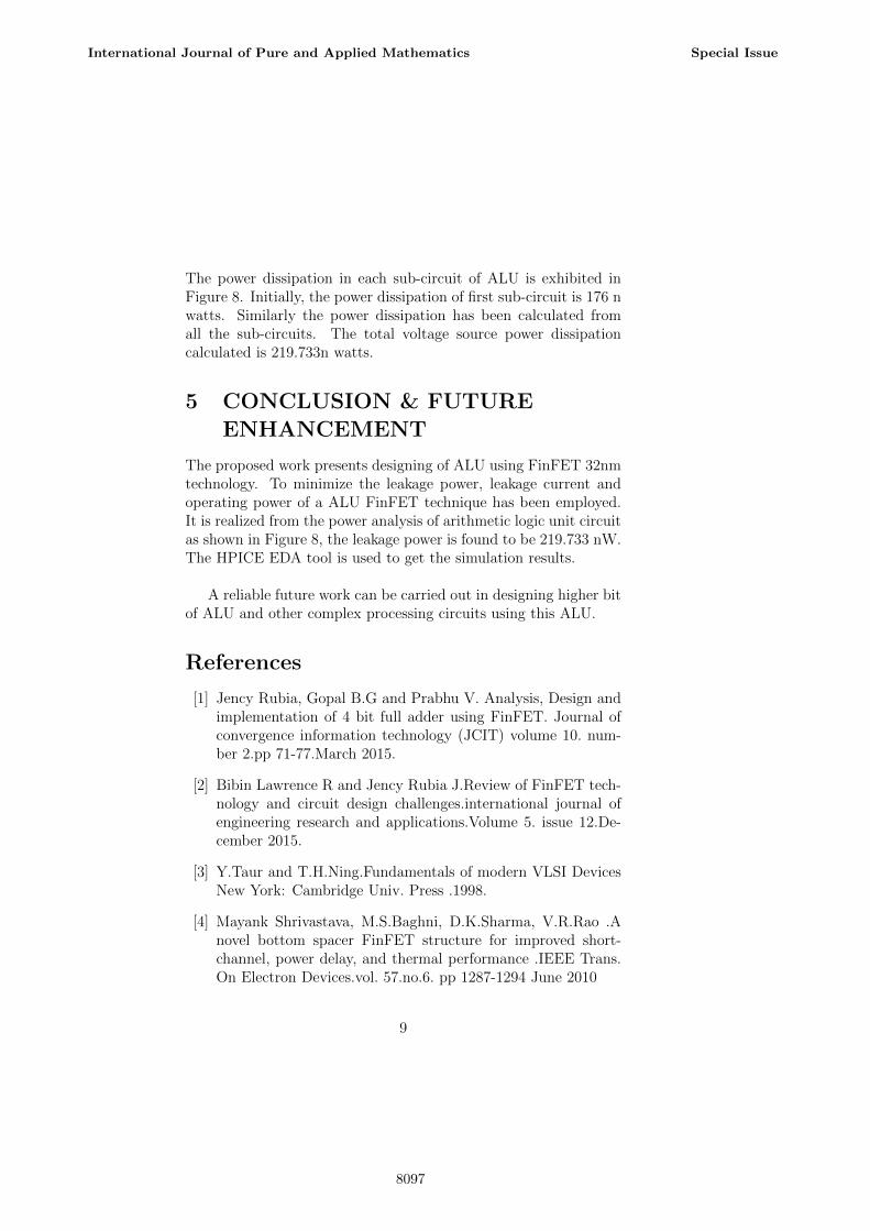
Input and the output waveforms are shown in Figure 5, 6 and Figure7 respectively for ALU circuit. The proposed ALU circuit has 2inputs, one carry input and 3 select lines. The resulted output isthe functional output and Carry out. The Figure 5 explains about2 inputs and carry input which are A, B, Cin waveforms.
7
International Journal of Pure and Applied Mathematics Special Issue
8095
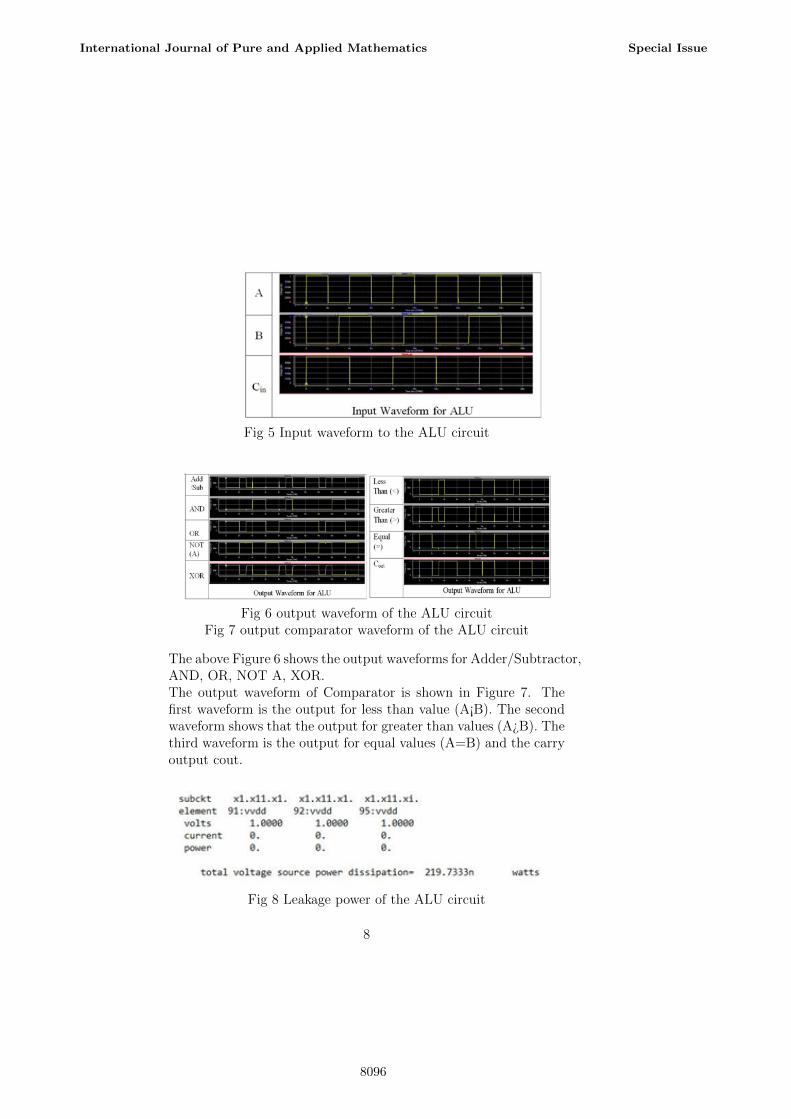
Fig 5 Input waveform to the ALU circuit
Fig 6 output waveform of the ALU circuitFig 7 output comparator waveform of the ALU circuit
The above Figure 6 shows the output waveforms for Adder/Subtractor,AND, OR, NOT A, XOR.The output waveform of Comparator is shown in Figure 7. Thefirst waveform is the output for less than value (A¡B). The secondwaveform shows that the output for greater than values (A¿B). Thethird waveform is the output for equal values (A=B) and the carryoutput cout.
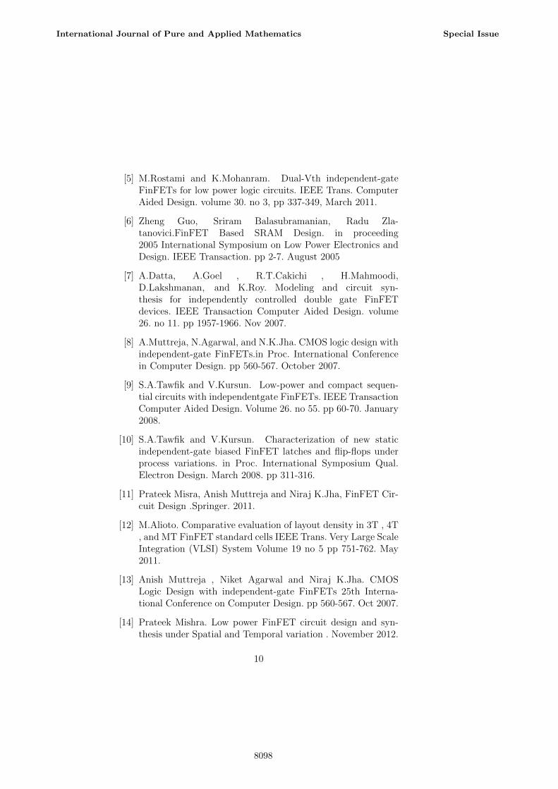
Fig 8 Leakage power of the ALU circuit
8
International Journal of Pure and Applied Mathematics Special Issue
8096
The power dissipation in each sub-circuit of ALU is exhibited inFigure 8. Initially, the power dissipation of first sub-circuit is 176 nwatts. Similarly the power dissipation has been calculated fromall the sub-circuits. The total voltage source power dissipationcalculated is 219.733n watts.
5 CONCLUSION & FUTURE
ENHANCEMENT
The proposed work presents designing of ALU using FinFET 32nmtechnology. To minimize the leakage power, leakage current andoperating power of a ALU FinFET technique has been employed.It is realized from the power analysis of arithmetic logic unit circuitas shown in Figure 8, the leakage power is found to be 219.733 nW.The HPICE EDA tool is used to get the simulation results.
A reliable future work can be carried out in designing higher bitof ALU and other complex processing circuits using this ALU.
References
[1] Jency Rubia, Gopal B.G and Prabhu V. Analysis, Design andimplementation of 4 bit full adder using FinFET. Journal ofconvergence information technology (JCIT) volume 10. num-ber 2.pp 71-77.March 2015.
[2] Bibin Lawrence R and Jency Rubia J.Review of FinFET tech-nology and circuit design challenges.international journal ofengineering research and applications.Volume 5. issue 12.De-cember 2015.
[3] Y.Taur and T.H.Ning.Fundamentals of modern VLSI DevicesNew York: Cambridge Univ. Press .1998.
[4] Mayank Shrivastava, M.S.Baghni, D.K.Sharma, V.R.Rao .Anovel bottom spacer FinFET structure for improved short-channel, power delay, and thermal performance .IEEE Trans.On Electron Devices.vol. 57.no.6. pp 1287-1294 June 2010
9
International Journal of Pure and Applied Mathematics Special Issue
8097
[5] M.Rostami and K.Mohanram. Dual-Vth independent-gateFinFETs for low power logic circuits. IEEE Trans. ComputerAided Design. volume 30. no 3, pp 337-349, March 2011.
[6] Zheng Guo, Sriram Balasubramanian, Radu Zla-tanovici.FinFET Based SRAM Design. in proceeding2005 International Symposium on Low Power Electronics andDesign. IEEE Transaction. pp 2-7. August 2005
[7] A.Datta, A.Goel , R.T.Cakichi , H.Mahmoodi,D.Lakshmanan, and K.Roy. Modeling and circuit syn-thesis for independently controlled double gate FinFETdevices. IEEE Transaction Computer Aided Design. volume26. no 11. pp 1957-1966. Nov 2007.
[8] A.Muttreja, N.Agarwal, and N.K.Jha. CMOS logic design withindependent-gate FinFETs.in Proc. International Conferencein Computer Design. pp 560-567. October 2007.
[9] S.A.Tawfik and V.Kursun. Low-power and compact sequen-tial circuits with independentgate FinFETs. IEEE TransactionComputer Aided Design. Volume 26. no 55. pp 60-70. January2008.
[10] S.A.Tawfik and V.Kursun. Characterization of new staticindependent-gate biased FinFET latches and flip-flops underprocess variations. in Proc. International Symposium Qual.Electron Design. March 2008. pp 311-316.
[11] Prateek Misra, Anish Muttreja and Niraj K.Jha, FinFET Cir-cuit Design .Springer. 2011.
[12] M.Alioto. Comparative evaluation of layout density in 3T , 4T, and MT FinFET standard cells IEEE Trans. Very Large ScaleIntegration (VLSI) System Volume 19 no 5 pp 751-762. May2011.
[13] Anish Muttreja , Niket Agarwal and Niraj K.Jha. CMOSLogic Design with independent-gate FinFETs 25th Interna-tional Conference on Computer Design. pp 560-567. Oct 2007.
[14] Prateek Mishra. Low power FinFET circuit design and syn-thesis under Spatial and Temporal variation . November 2012.
10
International Journal of Pure and Applied Mathematics Special Issue
8098
[15] Indraneel Suryavanshi, Ajit Gangad and PrathameshChodankar. Design of 1-bit Full Adder using FinFET. Inter-national Journal of Applied Engineering Research. vol.8. no.19. 2013.
[16] International Technology Roadmap for Semiconductors.Semiconductor Industry Association.[Online] Available :http://public.itrs.net
[17] Design of High-performance digital logic circuits based on Fin-FET technology. International Journal of Computer Applica-tions. pp 40-44 March 2012.
11
International Journal of Pure and Applied Mathematics Special Issue
8099

8100