Embed Size (px)
Citation preview
Design of High voltage power supply and
modulator for compact C-Band High Power
Radar Transmitter
Sushma B R
1, Venkatesh Prabhu
1
Ajith kumar N2 , Mohan H R
2, Madhusudhan R
2
1 LRDE, C.V. Raman Nagar, Bangalore – 560 093
2BEL, Bangalore – 560 013
[email protected] Abstract
This paper presents the design issues and challenges in the
realization of state of art compact high voltage power supply
and grid modulator for high performance TWT based C Band
Transmitter. The design goal was to achieve stable operation of
the transmitter having spectrum purity of near carrier noise of
-75dBc/Hz at 100 Hz away from the carrier while delivering 70
kW (minimum) of peak power and 3 kW of average power
across the bandwidth of 400MHz at C-Band. These
requirements translates into High Voltage Power Supply
(HVPS) design, i.e., Cathode voltage of -39 kVDC and Collector
voltage of 27kVDC with stringent cathode pulse to pulse
regulation of the order of 0.0004%, under adverse
environmental conditions which includes operation at altitudes
of 16000feet. High voltage power supply is the most critical unit
in TWT based transmitters. The realization of the pre-regulator
using power factor controlled interleaved boost converter,
realization of compact HVPS with single tapped high voltage
high frequency transformer are discussed in detail. Design of
compact modulator for the TWT is also discussed in detail.
Key words: Interleaved Boost converter, cross regulation.
I INTRODUCTION
Radar transmitters with high stability and high gain use
coherent amplifiers. One such amplifier is a Travelling
Wave Tube Amplifier (TWTA). This paper presents the
challenges involved in the design of a compact high
voltage power supply of a Travelling Wave Tube (TWT)
based transmitter.
High gain TWTAs require a very high peak power of few
tens of kW and high voltages of tens of kilovolts. The
power supply should be capable of delivering this high
power at high voltages in adverse EMI environment. The
performance specifications of these supplies are very
stringent demanding very good regulation on pulse to pulse
basis (0.0004%) with good efficiency.
State of art techniques like high switching frequency
inverter, PFC based interleaved boost converter as pre
regulator and single tapped High Voltage High Frequency
(HVHF) transformer resulted in a compact high voltage
power supply for a C-Band TWT based Transmitter with
peak RF output power of 70kW meeting very stringent
performance specifications.
The cathode and collector power supply for the TWT is
realized by a single inverter and tapped transformer fed
from a pre regulator. Cathode voltage is regulated by phase
modulation technique and the collector voltage is
maintained by the cross regulation of the HVHF
transformer. Phase Modulated Series Resonant Converter
(PM-SRC) operating at 50 kHz, with Zero Voltage
Switching (ZVS) is used as the inverter circuit topology for
its compactness, flexibility, efficiency and better dynamics.
The design realization of the Boost converter, PM-SRC
and cross regulation of HVHF transformer and realization
of high frequency modulator are discussed in detail.
II SYSTEM DESCRIPTION
Transmitter for Weapon locating Radar is realized in
volume of 1.2m3
and a weight of 575Kg, which constitutes
of the High Voltage Power supply, Control and protection
Unit (CPC), modulator and the microwave components.
Compact high Voltage power Supply is realized for the C-
band transmitter with the following main specifications.
Parameter Specifications
Output Power 20 kW
Input Voltage 3 Phase 415V, 50Hz
Input THD 30%
DC Ripple(Pre-regulator) <3V on full load
DC regulation(Pre-regulator) <0.5%
Cathode voltage and regulation -39kVDC,<0.0004% Pulse to pulse
Collector voltage 27kVDC ±1kV
The main blocks in which the compact high voltage Power
supply is realized is given in Fig.1 The High voltage power
supply is realized with a phase modulated series resonant
inverter, fed by a PFC based Boost regulator, followed by
a HVHF transformer with a inbuilt rectifier feeding High
voltage energy storage capacitors.
9th International Radar Symposium India - 2013 (IRSI - 13)
NIMHANS Convention Centre, Bangalore INDIA 1 10-14 December 2013
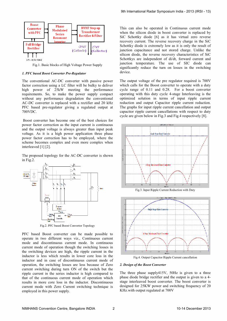
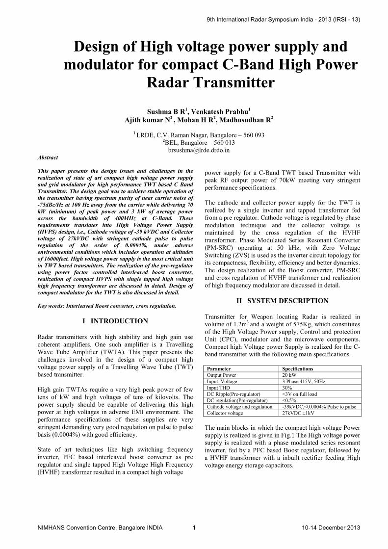
Fig.1. Basic blocks of High Voltage Power Supply
1. PFC based Boost Converter Pre-Regulator
The conventional AC-DC converter with passive power
factor correction using a LC filter will be bulky to deliver
high power of 25kW meeting the performance
requirements. So, to make the power supply compact
without any performance degradation the conventional
AC-DC converter is replaced with a rectifier and 20 kHz
PFC based pre-regulator giving a regulated output at
700VDC.
Boost converter has become one of the best choices for
power factor correction as the input current is continuous
and the output voltage is always greater than input peak
voltage. As it is a high power application three phase
power factor correction has to be employed, where the
scheme becomes complex and even more complex when
interleaved [1] [2].
The proposed topology for the AC-DC converter is shown
in Fig.2.
Fig.2. PFC based Boost Convertor Topology
PFC based Boost converter can be made possible to
operate in two different ways viz., Continuous current
mode and discontinuous current mode. In continuous
current mode of operation though the switching losses in
the switching devices are high, the ripple current in the
inductor is less which results in lower core loss in the
inductor and in case of discontinuous current mode of
operation, the switching losses are less because of Zero
current switching during turn ON of the switch but the
ripple current in the series inductor is high compared to
that of the continuous current mode of operation which
results in more core loss in the inductor. Discontinuous
current mode with Zero Current switching technique is
employed in this power supply.
This can also be operated in Continuous current mode
when the silicon diode in boost converter is replaced by
SiC Schottky diode [6] as it has virtual zero reverse
recovery current. The reverse recovery charge in the SiC
Schottky diode is extremely low as it is only the result of
junction capacitance and not stored charge. Unlike the
silicon diode, the reverse recovery characteristics of SiC
Schottkys are independent of di/dt, forward current and
junction temperature. The use of SIC diode can
significantly reduce the turn on losses in the switching
device.
The output voltage of the pre regulator required is 700V
which calls for the Boost converter to operate with a duty
cycle range of 0.11 and 0.28. For a boost converter
operating with this duty cycle 4-stage Interleaving is the
optimized solution in terms of input ripple current
reduction and output Capacitor ripple current reduction.
The graphs for input ripple current cancellation and output
capacitor ripple current cancellations with respect to duty
cycle are given below in Fig.3 and Fig.4 respectively [8].
Fig.3. Input Ripple Current Reduction with Duty
Fig.4. Output Capacitor Ripple Current cancellation
2. Design of the Boost Converter
The three phase supply415V, 50Hz is given to a three
phase diode bridge rectifier and the output is given to a 4-
stage interleaved boost converter. The boost converter is
designed for 25KW power and switching frequency of 20
KHz.with output regulated at 700V
9th International Radar Symposium India - 2013 (IRSI - 13)
NIMHANS Convention Centre, Bangalore INDIA 2 10-14 December 2013
The value of inductor and capacitor of the interleaved
Boost converter is given by the equations 1 and 2
respectively.
Inductor, L1 = L2 = L3 = L4
Vin_min2 *η *Ts Vout-(Vin_min*√ 2)
= ----------------------------------------------------------------- X ---------------------------------------------------------- … (1)
I% (Pout_max/4) Vout
where, Vin_min = Minimum input voltage
Vout = Output DC voltage
Ts= Time period of the PWM switching
Pout_max = Maximum output power
η = Efficiency
I% = Ratio of accepted peak to peak inductor
current ripple (typical value 20-40%)
Dmax*Ts
Capacitor, C = ------------------ …………….. (2)
Rload*% Ripple
where, Dmax = maximum duty cycle
Ts = Time period of the PWM switching
%Ripple = allowable output voltage ripple
Input supply current simulated and measured are shown in
Fig.5. The peak current drawn is 50A with an RMS value
of 34A. Input THD is measured to be 30%.
Fig.5.Simulated and measured input supply current
Four stage interleaved Boost converter is realized in DCM
mode and the voltage and current waveforms of the device
along with the switching pulses are shown in Fig. 6 and the
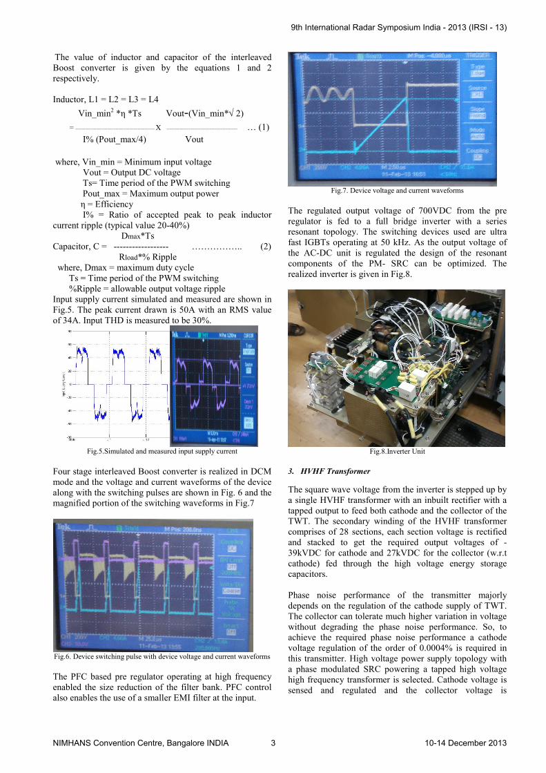
magnified portion of the switching waveforms in Fig.7
Fig.6. Device switching pulse with device voltage and current waveforms
The PFC based pre regulator operating at high frequency
enabled the size reduction of the filter bank. PFC control
also enables the use of a smaller EMI filter at the input.
Fig.7. Device voltage and current waveforms
The regulated output voltage of 700VDC from the pre
regulator is fed to a full bridge inverter with a series
resonant topology. The switching devices used are ultra
fast IGBTs operating at 50 kHz. As the output voltage of
the AC-DC unit is regulated the design of the resonant
components of the PM- SRC can be optimized. The
realized inverter is given in Fig.8.
Fig.8.Inverter Unit
3. HVHF Transformer
The square wave voltage from the inverter is stepped up by
a single HVHF transformer with an inbuilt rectifier with a
tapped output to feed both cathode and the collector of the
TWT. The secondary winding of the HVHF transformer
comprises of 28 sections, each section voltage is rectified
and stacked to get the required output voltages of -
39kVDC for cathode and 27kVDC for the collector (w.r.t
cathode) fed through the high voltage energy storage
capacitors.
Phase noise performance of the transmitter majorly
depends on the regulation of the cathode supply of TWT.
The collector can tolerate much higher variation in voltage
without degrading the phase noise performance. So, to
achieve the required phase noise performance a cathode
voltage regulation of the order of 0.0004% is required in
this transmitter. High voltage power supply topology with
a phase modulated SRC powering a tapped high voltage
high frequency transformer is selected. Cathode voltage is
sensed and regulated and the collector voltage is
9th International Radar Symposium India - 2013 (IRSI - 13)
NIMHANS Convention Centre, Bangalore INDIA 3 10-14 December 2013
maintained within the required limits by the cross
regulation of the transformer.
The high voltage cathode sample is fed to the feedback
loop of the control circuit through a compensated probe,
which produces phase shifted gate pulses for the IGBTs
resulting in the controlled primary voltage to the HVHF
transformer and in-turn the regulated output.
4. Cross Regulation of HVHF transformer
The Cathode output voltage of the rectifier stack in the
HVHF transformer is sensed and regulated to the desired
value by the feedback control loop of the PM-SRC. The
tapped output is not directly regulated, but are maintained
within tolerable limits with respect to the principle output
voltage by the coupling between the transformer windings
which is called cross regulation.
Cross regulation can be caused by many factors such as
transformer internal resistance, capacitance between coils
which causes the different coupling coefficients between
the coils which in-turn results in the leakage inductance.
The cross regulation becomes noticeable when the
difference in the output power between the secondary
windings of the tapped transformer is large.
The cross regulation in the multi-output transformer [7][8]
is affected by the leakage inductances of the transformer
windings. Proper winding patterns of the transformer
windings will lead to the improvement of the cross
regulation.
The value of leakage inductance depends on the winding
geometry in a transformer core. Changing the position of
the winding will change the value of the effective leakage
inductance. For better cross regulation, the leakage
inductances between the primary and secondary windings
should be small and the leakage inductance among the
secondary windings should be maximized to reduce the
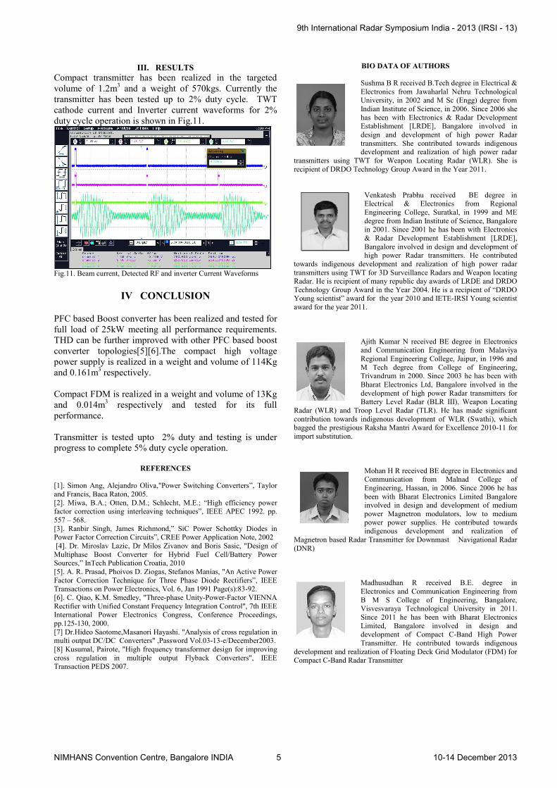
effect of load changes. The realized HVHF transformer is
shown in Fig.9.
Fig.9 HVHF Transformer
With the incorporation techniques discussed above the
HVPS unit is realized in a weight and volume of 114Kg
and 0.161m3.
5. Modulator
Modulator switches ON and OFF the beam of the TWT.
Two types of modulators are in use
• High power modulator
• Low power modulator
In high power modulation also called as cathode
modulation, high instantaneous powers are involved since
both the full beam voltage and current have to be switched
simultaneously. Low power modulators exploit a control
electrode such as grid, a focus electrode or an anode.
TWT’s generally use grid modulation, for switching ON
and OFF the beam. Grid modulation can be achieved
through Floating deck modulator (FDM) where all the
voltages generated are floating on the cathode potential of
few tens of kilovolts.
An isolation transformer provides input to FDM floating
on cathode potential of -39kVDC. To realize a compact
FDM and to reduce the size of the isolation transformer,
operating frequency of the isolation transformer is
enhanced to 30 kHz by a auxiliary converter and 100kHz
fly back converters are realized for generating grid and
filament voltages in FDM.
The auxiliary converter comprises of a 3 phase half bridge
diode rectifier generating 325VDC form 415V, 3phase
50Hz mains followed by a buck convertor operating at
60KHz with a output of 200VDC. A free running half
bridge inverter operating at 30kHz generates a 100V
square-wave voltage. A high frequency isolation
transformer operating at 30KHz provides AC input to the
modulator thereby reducing the size of the input filters of
the FDM.
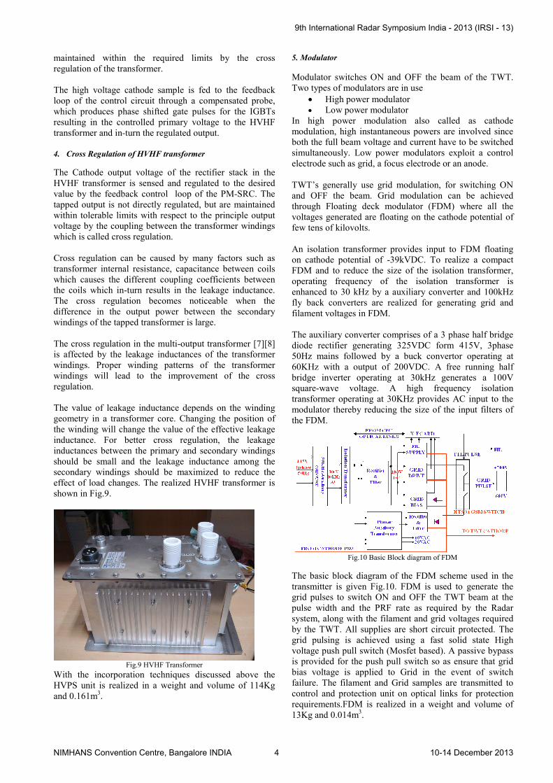
Fig.10 Basic Block diagram of FDM
The basic block diagram of the FDM scheme used in the
transmitter is given Fig.10. FDM is used to generate the
grid pulses to switch ON and OFF the TWT beam at the
pulse width and the PRF rate as required by the Radar
system, along with the filament and grid voltages required
by the TWT. All supplies are short circuit protected. The
grid pulsing is achieved using a fast solid state High
voltage push pull switch (Mosfet based). A passive bypass
is provided for the push pull switch so as ensure that grid
bias voltage is applied to Grid in the event of switch
failure. The filament and Grid samples are transmitted to
control and protection unit on optical links for protection
requirements.FDM is realized in a weight and volume of
13Kg and 0.014m3.
9th International Radar Symposium India - 2013 (IRSI - 13)
NIMHANS Convention Centre, Bangalore INDIA 4 10-14 December 2013
III. RESULTS
Compact transmitter has been realized in the targeted
volume of 1.2m3 and a weight of 570kgs. Currently the
transmitter has been tested up to 2% duty cycle. TWT
cathode current and Inverter current waveforms for 2%
duty cycle operation is shown in Fig.11.
Fig.11. Beam current, Detected RF and inverter Current Waveforms
IV CONCLUSION
PFC based Boost converter has been realized and tested for
full load of 25kW meeting all performance requirements.
THD can be further improved with other PFC based boost
converter topologies[5][6].The compact high voltage
power supply is realized in a weight and volume of 114Kg
and 0.161m3 respectively.
Compact FDM is realized in a weight and volume of 13Kg
and 0.014m3 respectively and tested for its full
performance.
Transmitter is tested upto 2% duty and testing is under
progress to complete 5% duty cycle operation.
REFERENCES
[1]. Simon Ang, Alejandro Oliva,"Power Switching Converters”, Taylor
and Francis, Baca Raton, 2005.
[2]. Miwa, B.A.; Otten, D.M.; Schlecht, M.E.; “High efficiency power factor correction using interleaving techniques”, IEEE APEC 1992. pp.
557 – 568.
[3]. Ranbir Singh, James Richmond,” SiC Power Schottky Diodes in Power Factor Correction Circuits”, CREE Power Application Note, 2002
[4]. Dr. Miroslav Lazic, Dr Milos Zivanov and Boris Sasic, "Design of
Multiphase Boost Converter for Hybrid Fuel Cell/Battery Power Sources,” InTech Publication Croatia, 2010
[5]. A. R. Prasad, Phoivos D. Ziogas, Stefanos Manias, "An Active Power
Factor Correction Technique for Three Phase Diode Rectifiers”, IEEE Transactions on Power Electronics, Vol. 6, Jan 1991 Page(s):83-92.
[6]. C. Qiao, K.M. Smedley, "Three-phase Unity-Power-Factor VIENNA
Rectifier with Unified Constant Frequency Integration Control", 7th IEEE International Power Electronics Congress, Conference Proceedings,
pp.125-130, 2000.
[7] Dr.Hideo Saotome,Masanori Hayashi. "Analysis of cross regulation in multi output DC/DC Converters" ,Password Vol.03-13-e/December2003.
[8] Kusumal, Pairote, "High frequency transformer design for improving
cross regulation in multiple output Flyback Converters", IEEE Transaction PEDS 2007.
BIO DATA OF AUTHORS
Sushma B R received B.Tech degree in Electrical &
Electronics from Jawaharlal Nehru Technological University, in 2002 and M Sc (Engg) degree from
Indian Institute of Science, in 2006. Since 2006 she
has been with Electronics & Radar Development Establishment [LRDE], Bangalore involved in
design and development of high power Radar
transmitters. She contributed towards indigenous development and realization of high power radar
transmitters using TWT for Weapon Locating Radar (WLR). She is
recipient of DRDO Technology Group Award in the Year 2011.
Venkatesh Prabhu received BE degree in Electrical & Electronics from Regional
Engineering College, Suratkal, in 1999 and ME
degree from Indian Institute of Science, Bangalore in 2001. Since 2001 he has been with Electronics
& Radar Development Establishment [LRDE],
Bangalore involved in design and development of high power Radar transmitters. He contributed
towards indigenous development and realization of high power radar
transmitters using TWT for 3D Surveillance Radars and Weapon locating Radar. He is recipient of many republic day awards of LRDE and DRDO
Technology Group Award in the Year 2004. He is a recipient of “DRDO Young scientist” award for the year 2010 and IETE-IRSI Young scientist
award for the year 2011.
Ajith Kumar N received BE degree in Electronics and Communication Engineering from Malaviya
Regional Engineering College, Jaipur, in 1996 and
M Tech degree from College of Engineering, Trivandrum in 2000. Since 2003 he has been with
Bharat Electronics Ltd, Bangalore involved in the
development of high power Radar transmitters for Battery Level Radar (BLR III), Weapon Locating
Radar (WLR) and Troop Level Radar (TLR). He has made significant
contribution towards indigenous development of WLR (Swathi), which bagged the prestigious Raksha Mantri Award for Excellence 2010-11 for
import substitution.
Mohan H R received BE degree in Electronics and Communication from Malnad College of
Engineering, Hassan, in 2006. Since 2006 he has
been with Bharat Electronics Limited Bangalore involved in design and development of medium
power Magnetron modulators, low to medium
power power supplies. He contributed towards indigenous development and realization of
Magnetron based Radar Transmitter for Downmast Navigational Radar
(DNR)
Madhusudhan R received B.E. degree in
Electronics and Communication Engineering from
B M S College of Engineering, Bangalore, Visvesvaraya Technological University in 2011.
Since 2011 he has been with Bharat Electronics
Limited, Bangalore involved in design and development of Compact C-Band High Power
Transmitter. He contributed towards indigenous
development and realization of Floating Deck Grid Modulator (FDM) for Compact C-Band Radar Transmitter
9th International Radar Symposium India - 2013 (IRSI - 13)
NIMHANS Convention Centre, Bangalore INDIA 5 10-14 December 2013