Embed Size (px)
Citation preview
DESIGN OF HIGH-SPEED SERIALLINKS IN CMOS
Chih-Kong Ken Yang
Technical Report No. CSL-TR-98-775
December 1998
Sponsored by Center for Integrated Systems,Sun Microsystems, and LSI Logic Inc.
i
DESIGN OF HIGH-SPEED SERIAL LINKS IN CMOS
Technical Report: CSL-TR-98-775
December 1998
Computer Systems LaboratoryDepartments of Electrical Engineering and Computer Science
Stanford UniversityStanford, California 94305-4055
Abstract
Demand for bandwidth in serial links has been increasing as the communications
industry demand higher quantity and quality of information. Whereas traditional gigabit
per second links has been in bipolar or GaAs, this research aims to push the use of CMOS
process technology in such links. Intrinsic gate speed limitations are overcome by
parallelizing the data. The on-chip frequency is maintained at a fraction (1/16) of the off-
chip data rate. Clocks with carefully controlled phases tapped from a local ring oscillator
are driven to a bank of input samplers to convert the serial bit stream into parallel data.
Similarly, the overlap of multiple-phased clocks are used to synchronize the multiplexing
of the parallel data onto the transmission line. To perform clock/data recovery, data is
further oversampled with finer phase separation and passed to digital logic. The digital
logic operates upon the samples to detect transitions in the bit stream to track the bit
boundaries. This tracking can operate at the cycle rate of the digital logic allowing
robustness to systematic phase noise. The challenge lies in the capturing of the high
frequency data stream and generating low jitter, accurately spaced clock edges. A test chip
is built demonstrating the transmission and recovery of a 4.0-Gb/s bit streams with < 10-14
bit-error rate using a 3x oversampled system in a 0.5-µm MOSIS CMOS process.
Key Words and Phrases: High Speed Signalling, Serial Links, Transmitters, Receivers,Phase-Locked Loops
Copyright © 1998
by
Chih-Kong Ken Yang

iii
Acknowledgments
During the course of this research and the writing of the dissertation, I have been
very fortunate to be surrounded by teachers, family, friends, and colleagues who have
continually offered me support, encouragement, and aid. I give my heartfelt thanks for
their contributions to my personal growth and research.
Academically, I am grateful for the supervision of three professors Mark Horowitz,
Bruce Wooley, and Tom Lee. They have been caches of valuable knowledge and advice. I
especially thank Mark Horowitz, who is the best research adviser one can hope for. I hope
through the years I’ve been able to pick up a little of his ability to see and explain ideas
and concepts with such clarity. I view all three of them as role models as I begin a career in
academics.
Throughout the ten years of college education, I am grateful for the support and
patience of my family. My mother and grandmother, who saw one sibling’s Ph.D. slip
away when he chose to pursue his dream in a business, was worried for some time for the
other, although never willing to show it. I thank their constant support. My brother, Jerry,
has always encouraged me to value the experience, and to take advantage of the unique
opportunities within a diverse institution at Stanford. I took his advice but embarrassingly,
I barely managed to pick up a shaggy golf swing.
iv
The environment at Stanford is full of brilliant and enthusiastic colleagues who
have provided valuable help and discussions. I wish to thank, in particular, the research
groups I have interacted with: past and present members of Mark’s research group, and the
research groups of Professor Kazovsky, Wooley, and Lee. I especially thank Stefanos
Sidiropoulos, with whom I began working on links and carried countless discussions,
Birdy Amrutur, who has been an intellectual wall to bounce ideas, Katy Falakshahi, who
has always brought new ideas and perspectives, and Ramin Farjad-Rad, whose help was
critical in completing my dissertation research. Beyond thanking all these people for their
help in my research, I thank and cherish their friendship.
Much of the research would not have been possible without the resources of Sun
Microsystems, Vitesse Semiconductor, LSI Logic Inc., and Rambus Inc.
Lastly, to all my dear friends who never forgot to check up on how I fared, thanks
so much for caring.
ix
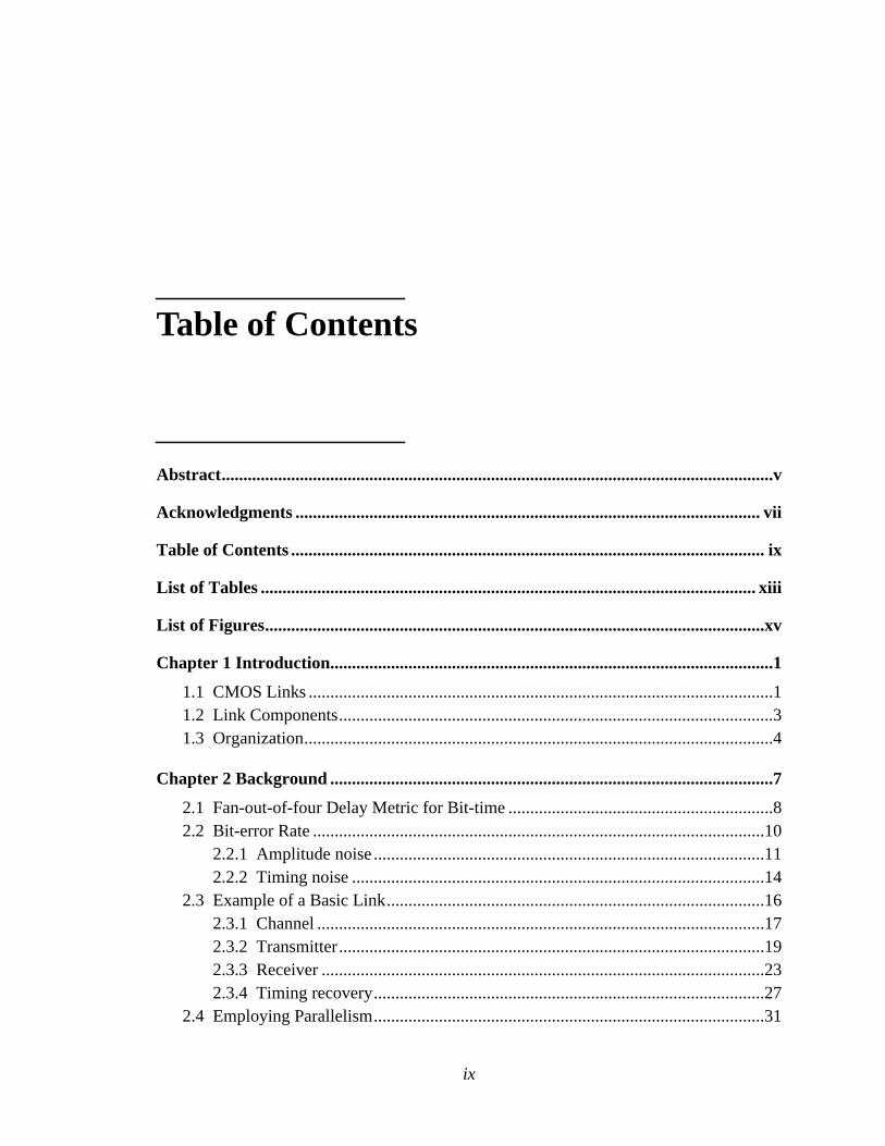
Table of Contents
Abstract...............................................................................................................................v
Acknowledgments ........................................................................................................... vii
Table of Contents ............................................................................................................. ix
List of Tables .................................................................................................................. xiii
List of Figures...................................................................................................................xv
Chapter 1 Introduction......................................................................................................1
1.1 CMOS Links ...........................................................................................................11.2 Link Components....................................................................................................31.3 Organization............................................................................................................4
Chapter 2 Background ......................................................................................................7
2.1 Fan-out-of-four Delay Metric for Bit-time .............................................................82.2 Bit-error Rate ........................................................................................................10
2.2.1 Amplitude noise..........................................................................................11 2.2.2 Timing noise ...............................................................................................14
2.3 Example of a Basic Link.......................................................................................16 2.3.1 Channel .......................................................................................................17 2.3.2 Transmitter..................................................................................................19 2.3.3 Receiver ......................................................................................................23 2.3.4 Timing recovery..........................................................................................27
2.4 Employing Parallelism..........................................................................................31
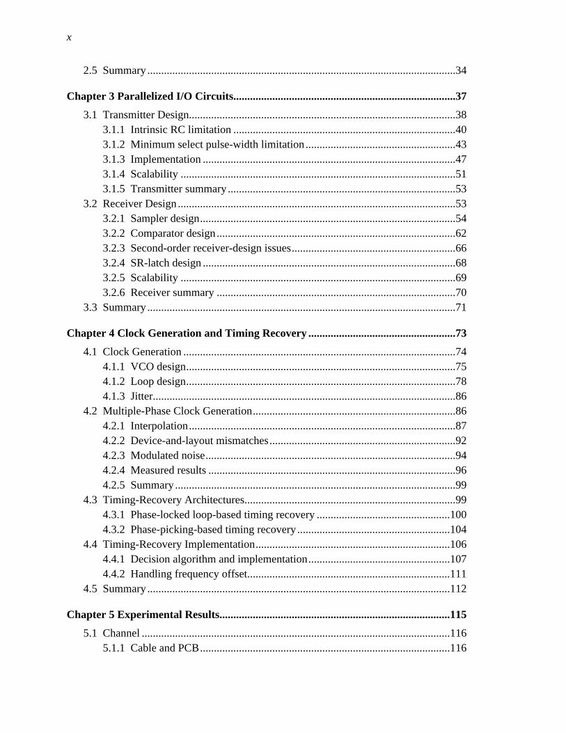
x
2.5 Summary...............................................................................................................34
Chapter 3 Parallelized I/O Circuits................................................................................37
3.1 Transmitter Design................................................................................................38 3.1.1 Intrinsic RC limitation ................................................................................40 3.1.2 Minimum select pulse-width limitation......................................................43 3.1.3 Implementation ...........................................................................................47 3.1.4 Scalability ...................................................................................................51 3.1.5 Transmitter summary..................................................................................53
3.2 Receiver Design....................................................................................................53 3.2.1 Sampler design............................................................................................54 3.2.2 Comparator design......................................................................................62 3.2.3 Second-order receiver-design issues...........................................................66 3.2.4 SR-latch design ...........................................................................................68 3.2.5 Scalability ...................................................................................................69 3.2.6 Receiver summary ......................................................................................70
3.3 Summary...............................................................................................................71
Chapter 4 Clock Generation and Timing Recovery .....................................................73
4.1 Clock Generation ..................................................................................................74 4.1.1 VCO design.................................................................................................75 4.1.2 Loop design.................................................................................................78 4.1.3 Jitter.............................................................................................................86
4.2 Multiple-Phase Clock Generation.........................................................................86 4.2.1 Interpolation................................................................................................87 4.2.2 Device-and-layout mismatches...................................................................92 4.2.3 Modulated noise..........................................................................................94 4.2.4 Measured results .........................................................................................96 4.2.5 Summary.....................................................................................................99
4.3 Timing-Recovery Architectures............................................................................99 4.3.1 Phase-locked loop-based timing recovery ................................................100 4.3.2 Phase-picking-based timing recovery .......................................................104
4.4 Timing-Recovery Implementation......................................................................106 4.4.1 Decision algorithm and implementation...................................................107 4.4.2 Handling frequency offset.........................................................................111
4.5 Summary.............................................................................................................112
Chapter 5 Experimental Results...................................................................................115
5.1 Channel ...............................................................................................................116 5.1.1 Cable and PCB..........................................................................................116
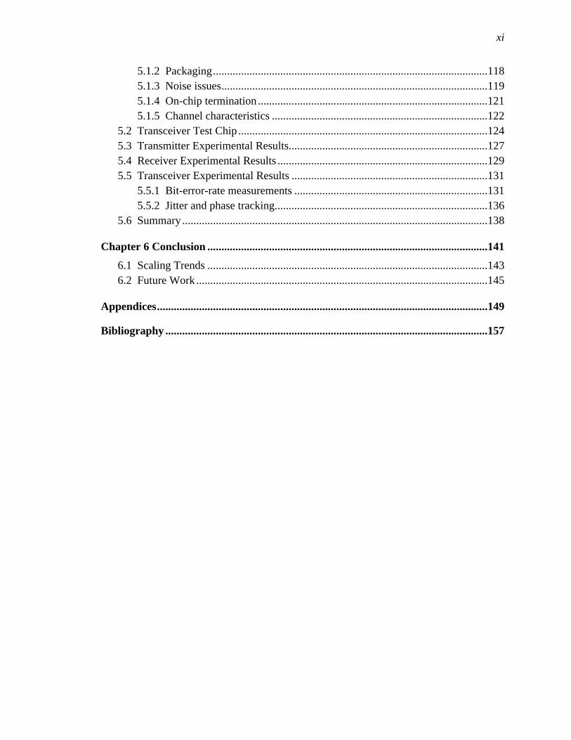
xi
5.1.2 Packaging..................................................................................................118 5.1.3 Noise issues...............................................................................................119 5.1.4 On-chip termination..................................................................................121 5.1.5 Channel characteristics .............................................................................122
5.2 Transceiver Test Chip.........................................................................................1245.3 Transmitter Experimental Results.......................................................................1275.4 Receiver Experimental Results ...........................................................................1295.5 Transceiver Experimental Results ......................................................................131
5.5.1 Bit-error-rate measurements .....................................................................131 5.5.2 Jitter and phase tracking............................................................................136
5.6 Summary.............................................................................................................138
Chapter 6 Conclusion ....................................................................................................141
6.1 Scaling Trends ....................................................................................................1436.2 Future Work........................................................................................................145
Appendices......................................................................................................................149
Bibliography ...................................................................................................................157

xii
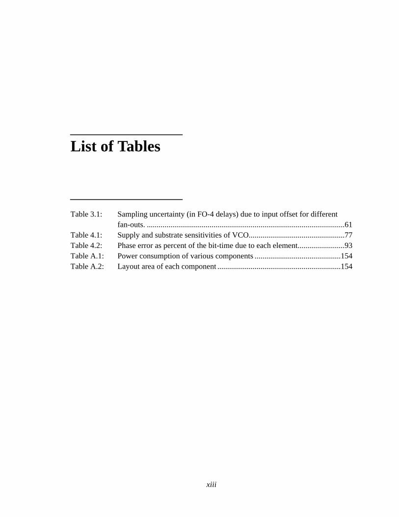
xiii
List of Tables
Table 3.1: Sampling uncertainty (in FO-4 delays) due to input offset for differentfan-outs. .....................................................................................................61
Table 4.1: Supply and substrate sensitivities of VCO.................................................77Table 4.2: Phase error as percent of the bit-time due to each element........................93Table A.1: Power consumption of various components ............................................154Table A.2: Layout area of each component ...............................................................154

xiv
xv
List of Figures
Figure 1.1: Technology fT comparison between GaAs, bipolar, and CMOS [34].........2Figure 1.2: Basic link components: the transmitter, the channel, and the receiver........3Figure 2.1: Fan-out of four inverter chain ......................................................................8Figure 2.2: FO-4 delay metric used for different circuits across process corners (a),
and FO-4 delay for different channel lengths (b).........................................9Figure 2.3: Illustration of a data eye. (a) shows a data stream, and (b) shows the
collapse of the data stream into a data eye.................................................10Figure 2.4: Effect of amplitude noise in (a) and phase noise in (b). ............................11Figure 2.5: BER (log) vsSNR (dB) ..............................................................................12Figure 2.6: Noise on a data eye showing superimposed large bounded noise
sources, and small unbounded (AWGN) noise sources.............................13Figure 2.7: SNR penalty for various phase offsets .......................................................15Figure 2.8: BER vsSNR with two different phase noiseσf. ........................................16Figure 2.9: Illustration of the channel including termination resistors and
packaging parasitics ...................................................................................18Figure 2.10: Transmitter timing diagram with different transmitter architectures:
voltage-mode (a), current-mode (b), and differential (c)...........................20Figure 2.11: Clock amplitude reduction (%) with clock period (in FO-4 delays). ........22Figure 2.12: Reduction in data eye due to ISI from an RC filter ...................................24Figure 2.13: Effect of finite input sensitivity and noise on the timing margin ..............24Figure 2.14: Receiver block diagram, timing diagram, and design examples:
(a) inverter, (b) differential pair, (c) latch..................................................25Figure 2.15: Common timing recovery architectures.....................................................29Figure 2.16: Block diagram of architecture with 2x parallelism on the transmitter
and receiver................................................................................................31
xvi
Figure 2.17: 2:1 multiplexer pulse width distortion versus bit-time ..............................32Figure 2.18: Tree type multiplexing using 2:1 multiplexing (showing a 4:1
multiplexer)................................................................................................32Figure 3.1: Higher order multiplexing, (a), and demultiplexing, (b) ...........................38Figure 3.2: N:1 multiplexer and its output bit-width reduction with decreasing
bit-width.....................................................................................................39Figure 3.3: (a) Pseudo-NMOS on-chip multiplexing pre-driver, and
(b) current-mode multiplexing output driver. ............................................40Figure 3.4: Multiplexing using overlapping pulses. The clock timing diagram is
shown in (a) and the schematic is shown in (b). [55] ................................43Figure 3.5: Transmitter multiplexing design using only two switches.
(a) shows the clock waveforms and (b) shows the schematics..................44Figure 3.6: (a) shows no ISI, (b) shows eye-amplitude reduction due to ISI,
(c) shows the bit amplitude degradation due to overlapping pulses withdecreasing overlap. ....................................................................................45
Figure 3.7: Percentage reduction on bit amplitude with reducing bit widths...............47Figure 3.8: Truly differential driver (a), with multiplexing (b)....................................48Figure 3.9: Different input configurations for the NAND structure output driver.......49Figure 3.10: Simulated transmitter data eyes .................................................................50Figure 3.11: Aperture defined for a sampler with switched resistance. (a) shows the
time domain signals for the switch, (b) shows the sampled impulseresponse, and (c) shows the sampled pulse response to a pulse ofwidth taper...................................................................................................55
Figure 3.12: Pass-gate sampler ON-resistance for various VGS (a) and as afunction of time (b) for a realistic clock waveform (simulated in a0.5-µm process technology.)......................................................................57
Figure 3.13: NMOS sampler’s “impulse response”, (a), and “step response”,(b) with various clock slew rates. The clock waveform for each of thecurves are shown in (c). .............................................................................59
Figure 3.14: Data-dependent uncertainty window due to input offset voltage. .............60Figure 3.15: Receiver (Sampler + comparator) design schematics................................63Figure 3.16: SR-latch structures that minimize data-dependent loading. ......................69Figure 4.1: PLL block diagram ....................................................................................74Figure 4.2: Voltage-controlled ring oscillator schematic. ............................................75Figure 4.3: Delay element and its biasing scheme using a half-buffer replica [64]
shown in (a), and the load element I-V characteristics in (b). ...................76Figure 4.4: Low-swing to high-swing converter ..........................................................78Figure 4.5: Power spectral density of phase noise of an oscillator with different
tracking bandwidths. ..................................................................................79Figure 4.6: Filter implementation using a series resistor for a zero. ............................80
xvii
Figure 4.7: 2nd-order charge pump PLL block diagram..............................................81Figure 4.8: Three different responses for over-, under-, and critically damped loop.
(a) shows the open-loop frequency response, and (b) shows closed-loopfrequency response. the time-domain response to a step in phase.............82
Figure 4.9: Three difference responses for over-, under-, and critically damped loop.(a) shows the time-domain response to a step in frequency, and(b) shows the time-domain response to a step in supply. ..........................83
Figure 4.10: Phase detector schematic (a), charge pump schematic (b), and phasedetector timing diagram in (c)....................................................................84
Figure 4.11: Filter implementation using proportional charge pump to implement thezero.............................................................................................................85
Figure 4.12: Clock phases tapped from a VCO and using interpolation for finerphase spacing. ............................................................................................87
Figure 4.13: Interpolation example with ideal integrator and with RC load..................88Figure 4.14: (a) shows the interpolator delay of interpolator with resistive loads for
two different interpolating clock spacing,s. (b) illustrates the percentageinterpolation error. .....................................................................................89
Figure 4.15: Interpolator schematics ..............................................................................90Figure 4.16: Interpolation error for six-stage oscillator .................................................91Figure 4.17: Receive-side layout floorplan (a) and layout (b) .......................................94Figure 4.18: Charge pump output waveform mismatch betweenUp andDown
causingVctrl ripple (a). Charge pump design introducing capacitanceto match theUp andDown time-constants. ...............................................95
Figure 4.19: Transmit-side DNL @ various frequencies ...............................................97Figure 4.20: Transmit-side DNL for 4 chips..................................................................97Figure 4.21: Receive-side DNL......................................................................................98Figure 4.22: Hogges phase detector for serial data. [7]................................................102Figure 4.23: Phase-picking architecture.......................................................................104Figure 4.24: Block diagram of decision logic ..............................................................107Figure 4.25: Example of decision algorithm ................................................................108Figure 4.26: Comparison of majority voting (unfilled-circle symbols) with
center-picking (filled-diamond symbols).................................................110Figure 5.1: SMA-connector board design (a), and die package attachment
diagram (b)...............................................................................................117Figure 5.2: Near-end crosstalk ...................................................................................119Figure 5.3: On-chip termination for current-mode driver and simulation results.
(a) shows off-chip termination (grey line), and (b) shows on-chiptermination (black line)............................................................................120
Figure 5.4: Transmitted data eye from the 0.35-µm process technology for5Gb/s........................................................................................................121
xviii
Figure 5.5: Differential-mode, (a), and common-mode, (b), TDR on the receiveside. The letters mark different locations on the package and board.......123
Figure 5.6: Board and package electrical model ........................................................124Figure 5.7: Transceiver chip’s block diagram............................................................125Figure 5.8: Transceiver chip micrograph ...................................................................126Figure 5.9: Measured data eye from the transmitter implemented in the
0.5-µm process.........................................................................................127Figure 5.10: Measured data eye for 0.35-µm chip operating at 6Gb/s.........................128Figure 5.11: Measured receiver offset demonstrated by the phase spacing DNL.
The average of the input offset for each device, not shown, is lessthan 1mV..................................................................................................130
Figure 5.12: BER measure test setup ...........................................................................132Figure 5.13: Measured BER vs.SNR...........................................................................133Figure 5.14: MeasuredSNR penalty with different phase offsets ................................134Figure 5.15: MeasuredSNR penalty at various common-mode voltage ......................135Figure 5.16: Measured BER at various input amplitude (the errors of this BER
measurement can be 6x at the larger signal amplitudes.) ........................136Figure 5.17: Clock jitter at 250MHz input frequency ..................................................137Figure 5.18: Data eye after inducing phase noise with a supply bump........................138Figure 6.1: Scaling of performance as technology scales ..........................................143Figure 6.2: Frequency response of a 10-m coaxial cable (RG55U) ...........................145Figure A.1: Timing and block diagram for receive-side re-synchronization ..............150Figure A.2: High MTBF flip-flop for synchronization ...............................................151Figure A.3: Timing and block diagram for transmit-side synchronization.................153Figure A.4: PRBS encoder: serial and parallel implementations................................155Figure A.5: PRBS decoder ..........................................................................................155
17
Chapter 1
Introduction
The increasing computational capability of processors is driving the need for high-
bandwidth links to communicate the information that is processed. Such links are often an
important part of multi-processor interconnection ([70], [30], and [52]), processor-to-
memory interfaces ([29] and [51]), and serial-network interfaces such as FireWire [98],
Ethernet ([94] and [58]), and SONET/FibreChannel ([10] and [75]). The research and
design of transmit and receive circuits for these links target increasing link speeds from
hundreds of Mb/s in current commodity links to Gb/s in the specifications for the next
generation links. The goal of this research is to demonstrate the capability of CMOS IC
technology in building the electronics for very high-bandwidth links, and to explore the
factors in this technology that limit a link’s data bandwidth.
1.1 CMOS LinksTraditionally, high-speed links in the Gb/s range have been implemented in GaAs or
bipolar technologies. The primary advantage provided by those technologies is faster
intrinsic device speed (higher fT).1However, despite its slower device speed, CMOS
1. For example, GaAs has an intrinsic carrier mobility of roughly 4000cm2/V-sec while CMOS electron
mobility is roughly 500 cm2/V-sec (NMOS). Bipolar transistors have higher fT (30GHz) and lowerparasitic junction capacitances.
18 Chapter 1: Introduction
technology is more widely available and allows higher integration than other technologies.
With this availability, high-speed links built in CMOS would appeal to large-volume
applications that require such links. Furthermore, with higher integration, links can be
built as a macro-block in a single-chip system allowing for significant cost savings in these
applications. Thus, determining what are the performance limits of CMOS links is an
important question to answer.
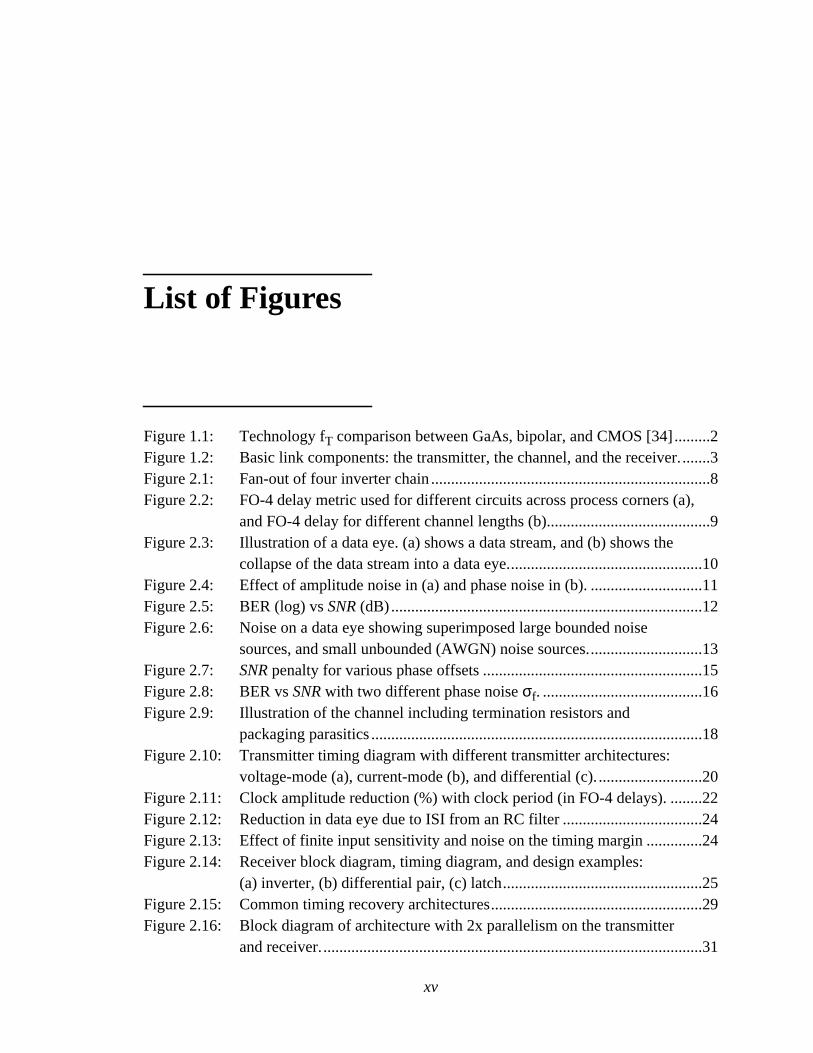
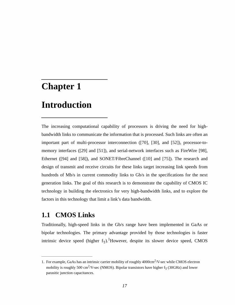
Another motivation for migrating to CMOS is the faster improvement of CMOS
speed than the speed of other technologies due to the rapid scaling of feature sizes. Figure
1.1 [34] shows the scaling trend of CMOS technology versus GaAs and bipolar
technologies in terms of the fT of the devices. The slopes of the figure indicate that a
CMOS technology will soon be available (in the 0.18-µm process technology) that has
speeds comparable to a 0.5-µm GaAs technology. Although it is always possible to yield
inherently better devices in non-traditional technologies such as SiGe heterojunctions, the
momentum and investment in CMOS technology development is progressing toward
making CMOS be the fastest commercial technology.
Figure 1.1: Technology fT comparison between GaAs, bipolar, and CMOS [34]
10GHz
1GHz
75 77 79 81 83 85 87 89 91 93
3µ
2µ1.5µ
1µ0.8µ
0.6µ
GaAs
Bipolar
MOS
fT
Year95 97 99
0.5µ0.35µ
0.25µ30GHz
100GHz
3GHz
Hemts, HBTs
1.2 Link Components 19
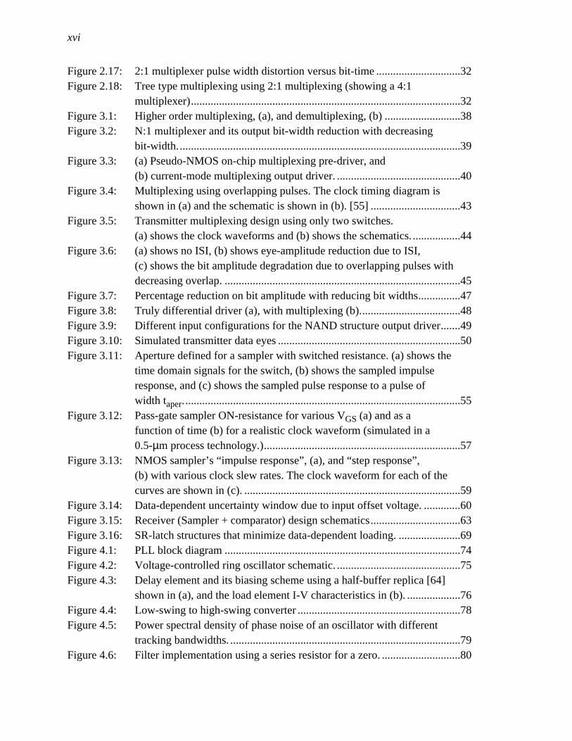
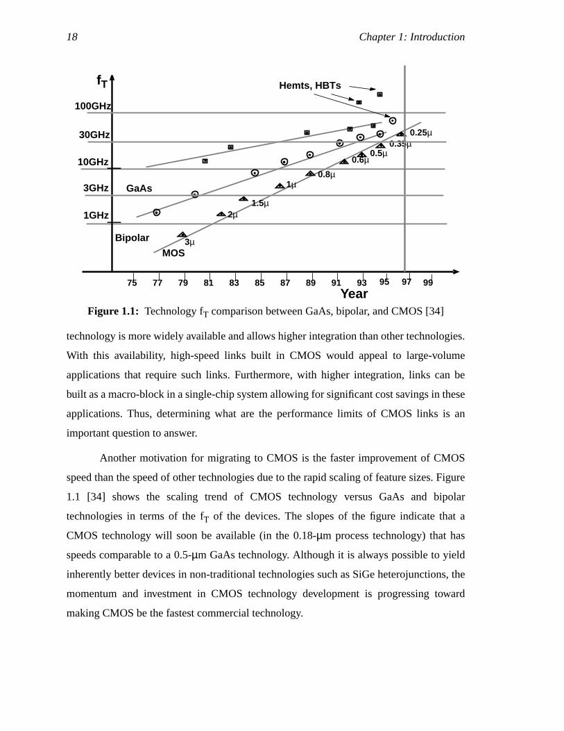
1.2 Link ComponentsA typical link is comprised of three primary components: a transmitter, a channel, and a
receiver. The transmitter converts digital bits into a signal stream that is propagated on the
channel to the receiver. The receiver reverts this analog signal back into binary data.
Figure 1.2 illustrates these components.
A transmitter sends the data as analog quantities or symbols. The analog values
used in this dissertation are simply either aHIGH-level orLOW-level to represent a single
bit — known as non-return-to-zero (NRZ). For example, in an optical system, the levels
are different amounts of optical power. For electrical systems, these levels are different
signal voltages. The duration of eachHIGH or LOW symbol is the bit-time. The difficulty
in a transmitter design is to maintain clean signal levels while transmitting high data rates.
The channel is the medium on which the data is propagated. This medium can
physically be an optical fiber, a coaxial transmission line, an unshielded twisted-pair, a
printed-circuit board (PCB) trace, or the chip package. The medium can attenuate or filter
the signal, and introduce noise. To achieve very high data rates, a channel with low
attenuation and distortion at high frequencies is necessary to reduce the noise and filtering.
To recover the bits from the signal, the analog waveform is amplified and sampled.
In order to recover the high-speed signals reliably, the circuits at the receiving end must be
able to resolve small inputs at very high rates, and time the sampling strobe correctly. The
receiver is the circuit that amplifies and samples the waveform while an additional circuit,
the timing-recovery circuit, properly places the sampling strobe.
Figure 1.2: Basic link components: the transmitter, the channel, and the receiver.
ReceiverTransmitter
Channel
TimingRecovery
Data out Data in
1001 1001
20 Chapter 1: Introduction
1.3 OrganizationThe performance limitations of each of these link components are the topics of the
following chapters. To begin discussing the limits of data rates in the transmitters and
receivers, Chapter 2 describes the architecture of a typical link, and introduces a
technology-normalized metric for bit-rate performance called a fan-out-of-four (FO-4)
delay. It also describes a second metric, bit-error rate, to measure the reliability of a link.
Based on these metrics, the chapter will show that a simple link can achieve a bit-width of
roughly 6-8 FO-4 delays. Employing parallelism can double the data rate, reducing the
bit-time to 3 FO-4 without increasing the on-chip frequency. The parallel architecture
multiplexes two on-chip data streams at a lower frequency to generate a higher data rate,
and demultiplexes the higher off-chip data rate at the receiver ([39], [51], and [86]).
To further push a link’s data bandwidth, Chapter 3 introduces architectures with
higher degree of parallelism. By using multiple clock phases, byte-wide parallel data are
multiplexed and demultiplexed for high data rates to be driven and received. This
technique maintains the lower on-chip digital processing frequency. The chapter describes
specific designs of the transmitter and receiver that demonstrate a data-rate performance of
less than one FO-4 delay and discusses the factors that limit the data rate. These
simulation results are later verified by the measurements in Chapter 5 from test chips built
in a 0.8-µm, 0.5-µm, and 0.35-µm CMOS technologies.
For these parallel architectures, the multiple clock phases, used to transmit and
sample the data, must be accurately spaced. Chapter 4 describes techniques to generate
these multiple phases. Errors in generating the phases can cause static phase-spacing
errors which compromise the transmitted bits and the sample positions for each bit. Data
presented in this chapter show that the errors are less than 10% of the desired phase
spacing between clocks in the technologies used.
Given the multiple clock phases, the phases must be properly placed to sample the
data with the best possible timing (timing recovery). There are two approaches toward
timing recovery: directly aligning the output of a control loop to the data (a data-recovery
phase-locked loop), or picking the correct sample after oversampling the data stream (a
phase-picking architecture). Since data-recovery PLL is more common, this chapter
1.3 Organization 21
describes phase picking and compares it to the phase-locked loop architecture. Although
performance is similar, phase-picking shows more robustness in a noisy environment. The
implementation of the phase-picking architecture used in the design is also described in
this chapter.
To validate the simulation data presented in the previous chapters, Chapter 5
discusses the measurement results from the implemented transceiver. The chapter begins
by characterizing the limitations of the test environment to ensure that the environment do
not introduce excessive bandwidth limitation or noise. Then, performance results are
presented showing a bit-error rate less than 10-14 from a 4-Gb/s test chip in a 0.5-µm
process technology (indicating a performance of one FO-4 delay as the bit-time).

22 Chapter 1: Introduction
23
Chapter 2
Background
A link’s performance can be evaluated based on many factors. For exploring the maximum
data rate of a given technology, two metrics in particular are used to evaluate various
designs: the bit-rate (or its inverse, the bit-time) and the bit-error rate.
The bit-time is usually measured in terms of nanoseconds or picoseconds. This
dissertation normalizes the bit-time by the speed of the CMOS technology. Since the
speed of many digital CMOS circuits scale with technology, this normalization allows us
to estimate the link’s speed in different technologies and extrapolate to future
technologies. The normalization factor used in this dissertation, the delay of a loaded
inverter, is described in the next section, and serves as the basic ruler for most of the
dissertation.
Since a link's receiver needs to convert an analog signal back into digital data,
there is always a probability for errors to occur. The second metric, bit-error rate (BER),
indicates the reliability of the link. A link’s maximum data rate is usually specified at a
specific BER (e.g. 10-9) to guarantee the robustness of the overall system. Section 2.2
describes how errors occur due to voltage or timing noise. To illustrate the effect of noise
on the system performance, the BER is shown as a function of the signal-to-noise ratio
(SNR) in a simplified analysis.
24 Chapter 2: Background
The design of a simple link is then discussed in Section 2.3. The section illustrates
how the signalling speed is primarily limited by the clock frequency. To further increase
the signalling rate, Section 2.4 examines how parallelism can be used to increase the link
speeds by transmitting and receiving two bits/clock-cycle, one bit in each half-cycle.
Other factors such as power, area, and latency are often considered when
discussing the performance of a link. Because this dissertation focuses on the maximum
bit-rate of a process technology, these factors are of secondary consideration.
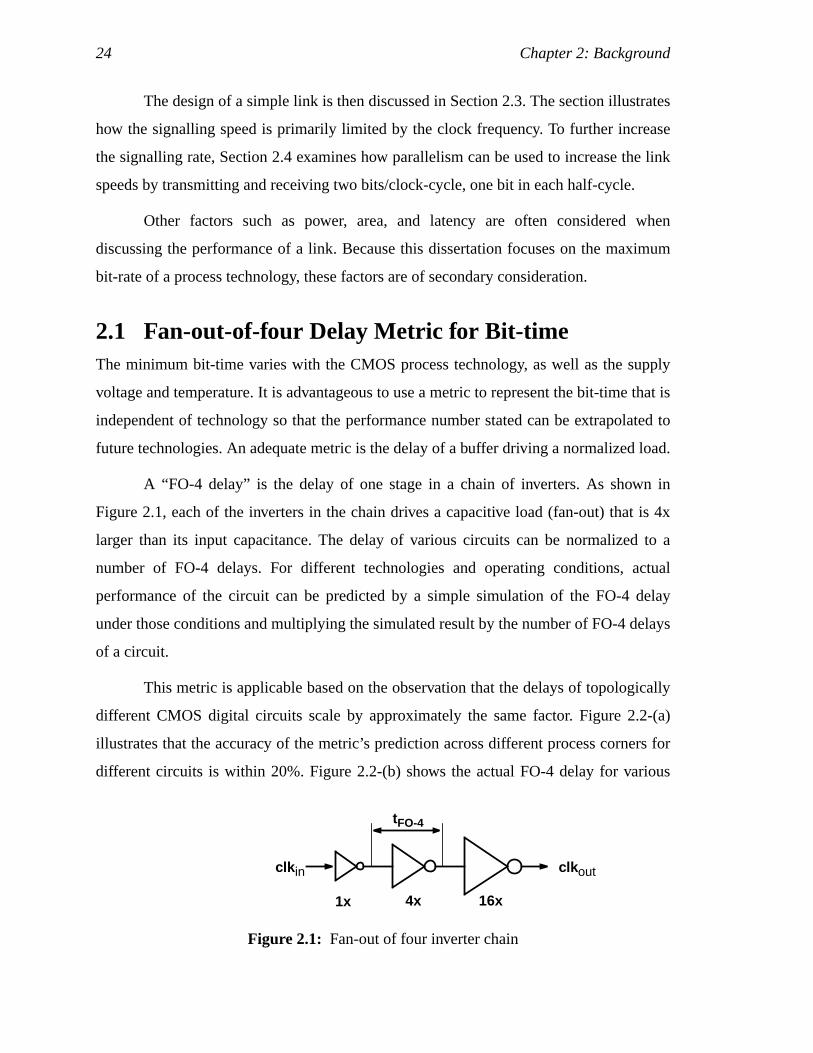
2.1 Fan-out-of-four Delay Metric for Bit-timeThe minimum bit-time varies with the CMOS process technology, as well as the supply
voltage and temperature. It is advantageous to use a metric to represent the bit-time that is
independent of technology so that the performance number stated can be extrapolated to
future technologies. An adequate metric is the delay of a buffer driving a normalized load.
A “FO-4 delay” is the delay of one stage in a chain of inverters. As shown in
Figure 2.1, each of the inverters in the chain drives a capacitive load (fan-out) that is 4x
larger than its input capacitance. The delay of various circuits can be normalized to a
number of FO-4 delays. For different technologies and operating conditions, actual
performance of the circuit can be predicted by a simple simulation of the FO-4 delay
under those conditions and multiplying the simulated result by the number of FO-4 delays
of a circuit.
This metric is applicable based on the observation that the delays of topologically
different CMOS digital circuits scale by approximately the same factor. Figure 2.2-(a)
illustrates that the accuracy of the metric’s prediction across different process corners for
different circuits is within 20%. Figure 2.2-(b) shows the actual FO-4 delay for various
Figure 2.1: Fan-out of four inverter chain
1x 4x 16x
tFO-4
clk in clk out
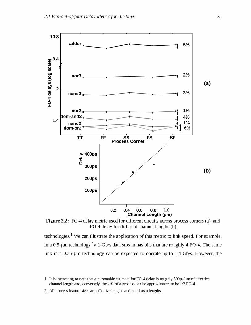
2.1 Fan-out-of-four Delay Metric for Bit-time 25
technologies.1 We can illustrate the application of this metric to link speed. For example,
in a 0.5-µm technology2 a 1-Gb/s data stream has bits that are roughly 4 FO-4. The same
link in a 0.35-µm technology can be expected to operate up to 1.4 Gb/s. However, the
1. It is interesting to note that a reasonable estimate for FO-4 delay is roughly 500ps/µm of effectivechannel length and, conversely, the1/fT of a process can be approximated to be 1/3 FO-4.
2. All process feature sizes are effective lengths and not drawn lengths.
Figure 2.2: FO-4 delay metric used for different circuits across process corners (a), andFO-4 delay for different channel lengths (b)
1.4
2
8.4
10.8
TT FF SS FS SF
FO
-4 d
elay
s (lo
g sc
ale)
Process Corner
adder 5%
nor3 2%
nand3 3%
nor2 1%dom-and2 4%
dom-or2 6%nand2 1%
400ps
300ps
200ps
100ps
Del
ay
0.2 0.4 0.6 0.8Channel Length ( µm)
1.0
(a)
(b)
26 Chapter 2: Background
underlying assumption is that the link performance scales with the same factor as the
scaling of FO-4 delay. This assumption will be experimentally verified in Chapter 5 where
results of a link built in three different processes are compared. The technologies used in
this dissertation are a 0.8-µm (Hewlett-Packard), a 0.5-µm (Hewlett-Packard), and a 0.35-
µm (LSI) technology. The FO-4 delays of Figure 2.2-(a) are for these technologies.
2.2 Bit-error RateThe second metric for link performance, bit-error rate, indicates the reliability of a link.
This reliability ties closely with the data-rate metric presented above because excessive
errors may force a link to operate at a lower data rate. The errors are due to noise on the
signal that is transmitted and noise in the receiving circuits. The noise can be divided into
phase noise and amplitude noise and each of them can be further broken down into static
and dynamic. Static noise is commonly referred to as phase or voltage offset.
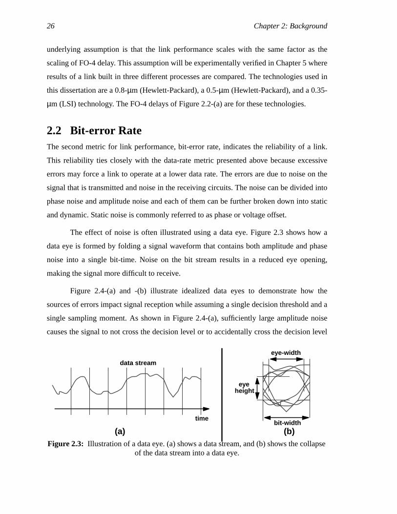
The effect of noise is often illustrated using a data eye. Figure 2.3 shows how a
data eye is formed by folding a signal waveform that contains both amplitude and phase
noise into a single bit-time. Noise on the bit stream results in a reduced eye opening,
making the signal more difficult to receive.
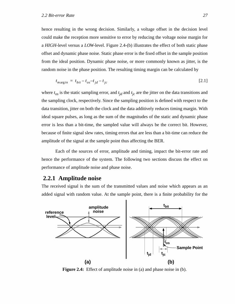
Figure 2.4-(a) and -(b) illustrate idealized data eyes to demonstrate how the
sources of errors impact signal reception while assuming a single decision threshold and a
single sampling moment. As shown in Figure 2.4-(a), sufficiently large amplitude noise
causes the signal to not cross the decision level or to accidentally cross the decision level
Figure 2.3: Illustration of a data eye. (a) shows a data stream, and (b) shows the collapseof the data stream into a data eye.
(a) (b)bit-width
eye-width
data stream
time
eyeheight
2.2 Bit-error Rate 27
hence resulting in the wrong decision. Similarly, a voltage offset in the decision level
could make the reception more sensitive to error by reducing the voltage noise margin for
a HIGH-level versus aLOW-level. Figure 2.4-(b) illustrates the effect of both static phase
offset and dynamic phase noise. Static phase error is the fixed offset in the sample position
from the ideal position. Dynamic phase noise, or more commonly known as jitter, is the
random noise in the phase position. The resulting timing margin can be calculated by
[2.1]
wheretos is the static sampling error, andtjd andtjc are the jitter on the data transitions and
the sampling clock, respectively. Since the sampling position is defined with respect to the
data transition, jitter on both the clock and the data additively reduces timing margin. With
ideal square pulses, as long as the sum of the magnitudes of the static and dynamic phase
error is less than a bit-time, the sampled value will always be the correct bit. However,
because of finite signal slew rates, timing errors that are less than a bit-time can reduce the
amplitude of the signal at the sample point thus affecting the BER.
Each of the sources of error, amplitude and timing, impact the bit-error rate and
hence the performance of the system. The following two sections discuss the effect on
performance of amplitude noise and phase noise.
2.2.1 Amplitude noiseThe received signal is the sum of the transmitted values and noise which appears as an
added signal with random value. At the sample point, there is a finite probability for the
Figure 2.4: Effect of amplitude noise in (a) and phase noise in (b).
noiseamplitude
referencelevel
(a)
tbit
tjctjd
tos
Sample Point
(b)
tm inarg tbit tos t jd–– t jc–=
28 Chapter 2: Background
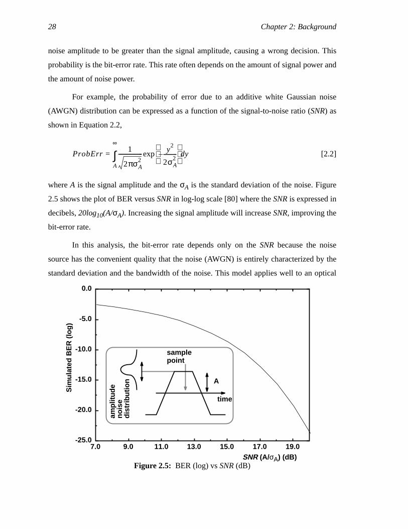
noise amplitude to be greater than the signal amplitude, causing a wrong decision. This
probability is the bit-error rate. This rate often depends on the amount of signal power and
the amount of noise power.
For example, the probability of error due to an additive white Gaussian noise
(AWGN) distribution can be expressed as a function of the signal-to-noise ratio (SNR) as
shown in Equation 2.2,
[2.2]
whereA is the signal amplitude and theσA is the standard deviation of the noise. Figure
2.5 shows the plot of BER versusSNR in log-log scale [80] where theSNR is expressed in
decibels,20log10(A/σA). Increasing the signal amplitude will increaseSNR, improving the
bit-error rate.
In this analysis, the bit-error rate depends only on theSNR because the noise
source has the convenient quality that the noise (AWGN) is entirely characterized by the
standard deviation and the bandwidth of the noise. This model applies well to an optical
ProbErr1
2πσA2
------------------ y2
2σA2
----------–
exp
A
∞
∫= yd
Figure 2.5: BER (log) vsSNR (dB)
7.0 9.0 11.0 13.0 15.0 17.0 19.0-25.0
-20.0
-15.0
-10.0
-5.0
0.0
Sim
ulat
ed B
ER
(lo
g)
SNR (A/σA) (dB)
ampl
itude
A
time
samplepoint
nois
edi
strib
utio
n
2.2 Bit-error Rate 29
system because of the optical receiver (typically a diode or resistor) has the AWGN noise
properties. Although this type of noise inherently exists in any system (e.g. thermal noise),
for electrical systems, AWGN noise sources are typically very low in power (and
amplitude) when compared to other types of noise that may be present in the link. For
example, noise can be coupled by signal switching which is correlated to the data and can
have a bounded probability distribution (unlike the Gaussian probability distribution).
Furthermore, these noise are often proportional to the signal amplitude. If many such
sources are present, the Central Limit Theorem [60] says that one can potentially
approximate the sum of many noise sources as Gaussian. However, it does not apply if the
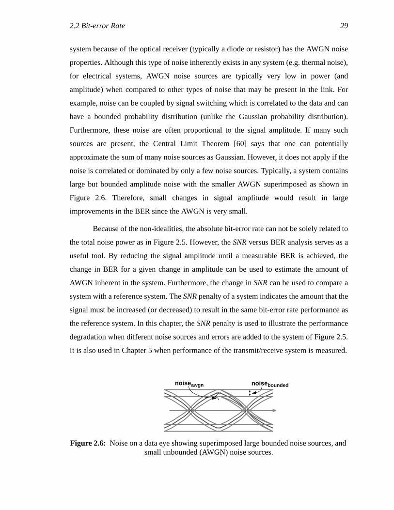
noise is correlated or dominated by only a few noise sources. Typically, a system contains
large but bounded amplitude noise with the smaller AWGN superimposed as shown in
Figure 2.6. Therefore, small changes in signal amplitude would result in large
improvements in the BER since the AWGN is very small.
Because of the non-idealities, the absolute bit-error rate can not be solely related to
the total noise power as in Figure 2.5. However, theSNR versus BER analysis serves as a
useful tool. By reducing the signal amplitude until a measurable BER is achieved, the
change in BER for a given change in amplitude can be used to estimate the amount of
AWGN inherent in the system. Furthermore, the change inSNR can be used to compare a
system with a reference system. TheSNRpenalty of a system indicates the amount that the
signal must be increased (or decreased) to result in the same bit-error rate performance as
the reference system. In this chapter, theSNR penalty is used to illustrate the performance
degradation when different noise sources and errors are added to the system of Figure 2.5.
It is also used in Chapter 5 when performance of the transmit/receive system is measured.
Figure 2.6: Noise on a data eye showing superimposed large bounded noise sources, andsmall unbounded (AWGN) noise sources.
noise boundednoise awgn
30 Chapter 2: Background
This method can be used to illustrate how a dc offset in the decision level can
degrade performance. The offset can be considered as a reduction of the signal amplitude
for one of the two signal levels. A decision level shifted higher byαA would reduce the
amplitude of theHIGH-level and increase the amplitude of theLOW-level. If HIGH’s and
LOW’s are equally probable in a data stream, the probability of error is the average of the
two probabilities. Since the probability increases exponentially with decreasingSNR, the
error rate is dominated by the signal value with the lowerSNR which, in this case, is due to
the HIGH pulse. This reduction in performance can be expressed as anSNR penalty of
20log10(1-α).
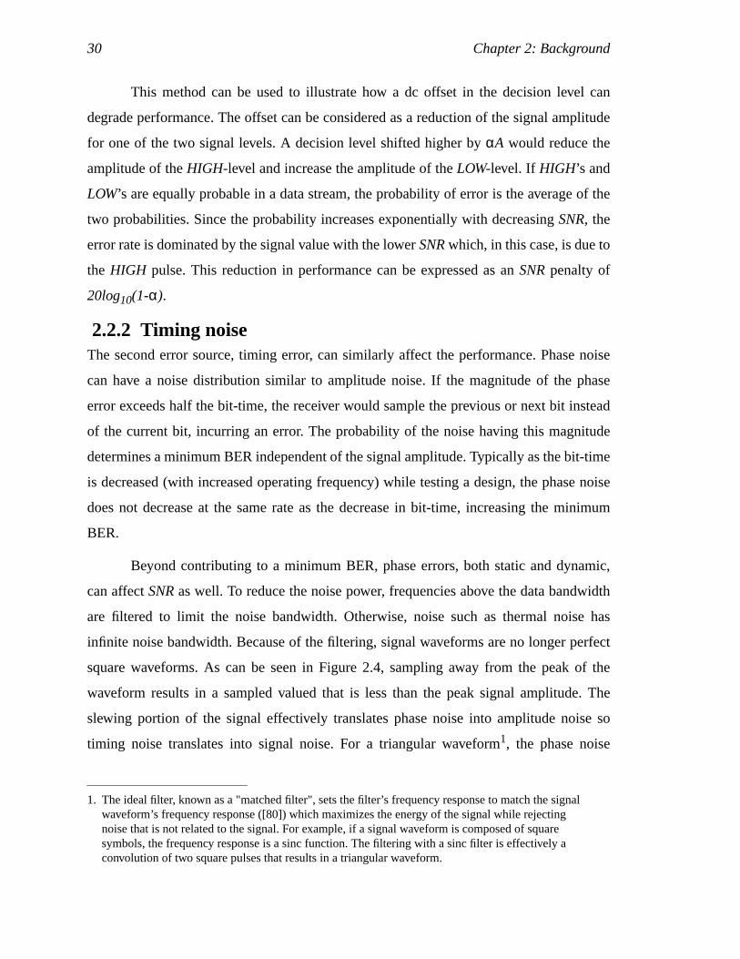
2.2.2 Timing noiseThe second error source, timing error, can similarly affect the performance. Phase noise
can have a noise distribution similar to amplitude noise. If the magnitude of the phase
error exceeds half the bit-time, the receiver would sample the previous or next bit instead
of the current bit, incurring an error. The probability of the noise having this magnitude
determines a minimum BER independent of the signal amplitude. Typically as the bit-time
is decreased (with increased operating frequency) while testing a design, the phase noise
does not decrease at the same rate as the decrease in bit-time, increasing the minimum
BER.
Beyond contributing to a minimum BER, phase errors, both static and dynamic,
can affectSNR as well. To reduce the noise power, frequencies above the data bandwidth
are filtered to limit the noise bandwidth. Otherwise, noise such as thermal noise has
infinite noise bandwidth. Because of the filtering, signal waveforms are no longer perfect
square waveforms. As can be seen in Figure 2.4, sampling away from the peak of the
waveform results in a sampled valued that is less than the peak signal amplitude. The
slewing portion of the signal effectively translates phase noise into amplitude noise so
timing noise translates into signal noise. For a triangular waveform1, the phase noise
1. The ideal filter, known as a "matched filter", sets the filter’s frequency response to match the signalwaveform’s frequency response ([80]) which maximizes the energy of the signal while rejectingnoise that is not related to the signal. For example, if a signal waveform is composed of squaresymbols, the frequency response is a sinc function. The filtering with a sinc filter is effectively aconvolution of two square pulses that results in a triangular waveform.
2.2 Bit-error Rate 31
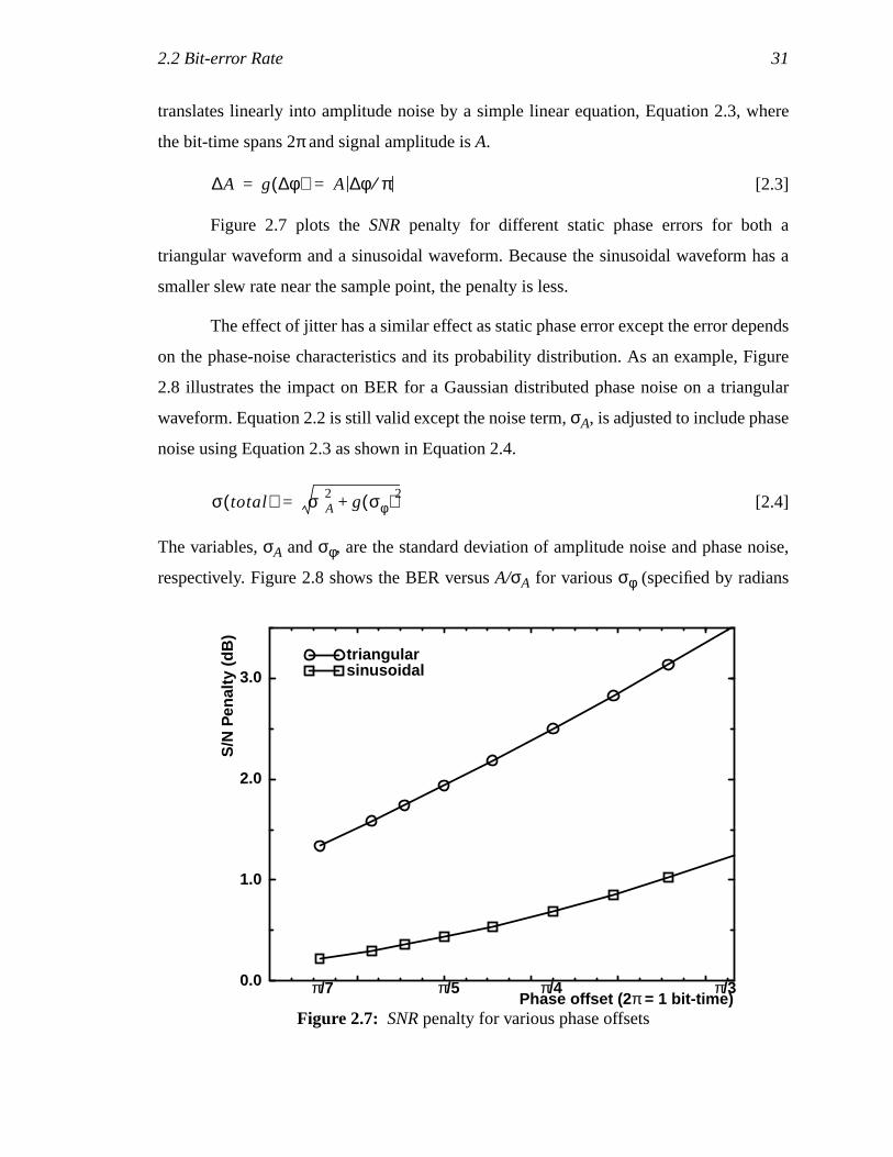
translates linearly into amplitude noise by a simple linear equation, Equation 2.3, where
the bit-time spans 2π and signal amplitude isA.
[2.3]
Figure 2.7 plots theSNR penalty for different static phase errors for both a
triangular waveform and a sinusoidal waveform. Because the sinusoidal waveform has a
smaller slew rate near the sample point, the penalty is less.
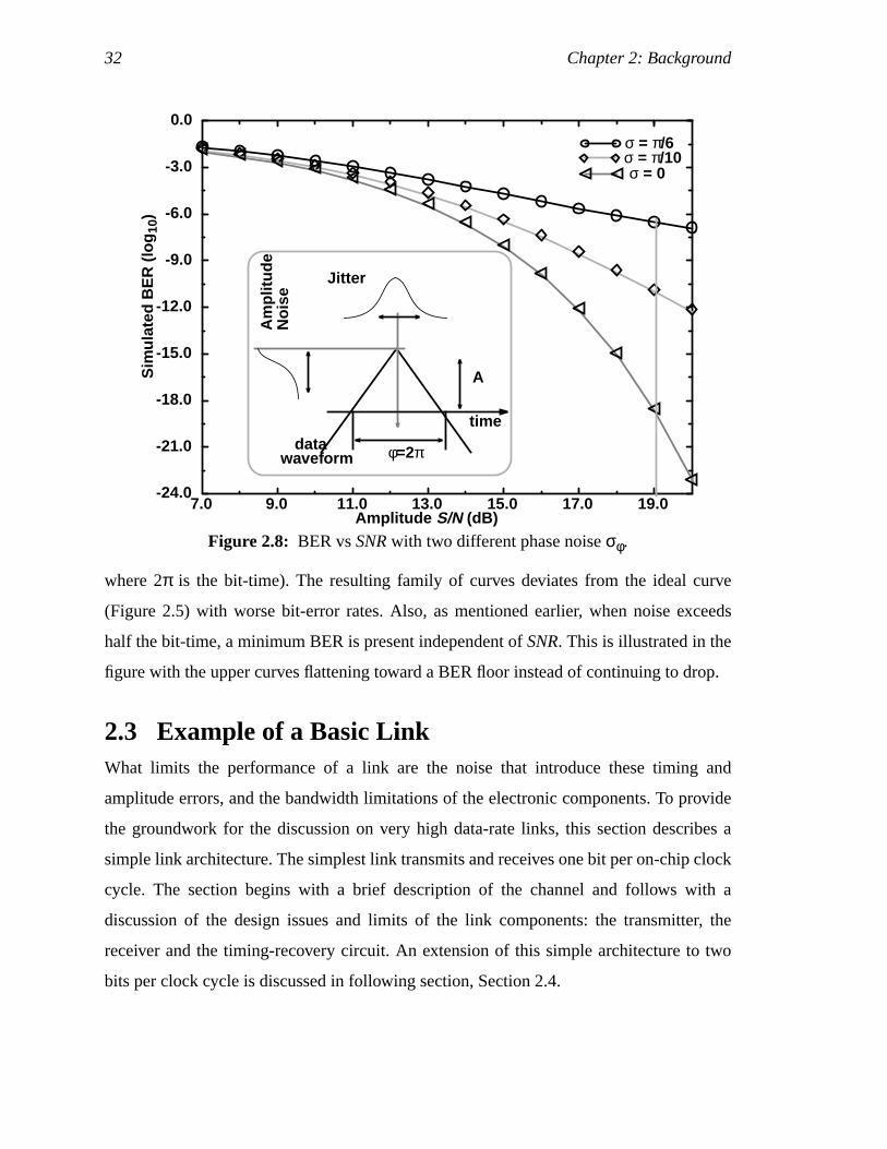
The effect of jitter has a similar effect as static phase error except the error depends
on the phase-noise characteristics and its probability distribution. As an example, Figure
2.8 illustrates the impact on BER for a Gaussian distributed phase noise on a triangular
waveform. Equation 2.2 is still valid except the noise term,σA, is adjusted to include phase
noise using Equation 2.3 as shown in Equation 2.4.
[2.4]
The variables,σA andσφ, are the standard deviation of amplitude noise and phase noise,
respectively. Figure 2.8 shows the BER versusA/σA for variousσφ (specified by radians
A∆ g φ∆( ) A φ π⁄∆= =
Figure 2.7: SNR penalty for various phase offsets
π/7 π/5 π/4 π/30.0
1.0
2.0
3.0triangularsinusoidal
Phase offset (2 π = 1 bit-time)
S/N
Pen
alty
(dB
)
σ total( ) σA2
g σφ( )2+=
32 Chapter 2: Background
where 2π is the bit-time). The resulting family of curves deviates from the ideal curve
(Figure 2.5) with worse bit-error rates. Also, as mentioned earlier, when noise exceeds
half the bit-time, a minimum BER is present independent ofSNR. This is illustrated in the
figure with the upper curves flattening toward a BER floor instead of continuing to drop.
2.3 Example of a Basic LinkWhat limits the performance of a link are the noise that introduce these timing and
amplitude errors, and the bandwidth limitations of the electronic components. To provide
the groundwork for the discussion on very high data-rate links, this section describes a
simple link architecture. The simplest link transmits and receives one bit per on-chip clock
cycle. The section begins with a brief description of the channel and follows with a
discussion of the design issues and limits of the link components: the transmitter, the
receiver and the timing-recovery circuit. An extension of this simple architecture to two
bits per clock cycle is discussed in following section, Section 2.4.
Figure 2.8: BER vsSNR with two different phase noiseσφ.
Sim
ulat
ed B
ER
(lo
g10
)
Amplitude S/N (dB)7.0 9.0 11.0 13.0 15.0 17.0 19.0
-24.0
-21.0
-18.0
-15.0
-12.0
-9.0
-6.0
-3.0
0.0σ = π/6σ = π/10σ = 0
JitterA
mpl
itude
A
φ=2πdatawaveform
time
Noi
se
2.3 Example of a Basic Link 33
2.3.1 ChannelThe channel is the entire path from the output of the transmitter circuit to the input to the
receiver circuit. This includes the connection from the chip input/output pad to the
package pin as well as any PCB trace and coaxial cables used to connect the packages
together. The path can be characterized as a conductor that carries the signal together with
a nearby return path for the signal current to close the circuit.
The return path is the signal’s reference. For single-ended signals, the reference is
the power planes on a PCB, or the shield of a cable. For differential signals, the reference
is embedded in the signal as the opposite polarity. Because the signal is commonly tightly
coupled to its reference, proper reception of a signal is with respect to this reference. It is
primarily the noise that is coupled differentially between the signal and the reference that
degrades link performance. Noise that couples equally onto the reference and to the signal
appears as a common-mode noise that most receivers are able to reject. Noise rejection by
receivers will be further discussed in Section 2.3.3.
The circuit for the signalling medium can be modeled as distributed energy-storage
elements, inductance (L/meter) and capacitance (C/meter), that propagate the energy of a
signal with some small loss, known as a transmission line. The geometry and material of
the line determines theL and C. To the signal source, these transmission lines appear
electrically as a real impedance, known as the characteristic impedance, with value of
which is typically between 50- and 100Ω.
Losses occur in the propagation due to radiated losses, dielectric loss, and resistive
losses in the conductor. These losses are often frequency dependent, which filters and
limits the bandwidth of the signal. For example, at higher frequencies, current flows closer
to the surface of the conductor hence reducing the area of current flow and increasing the
resistive loss, a phenomenon known as skin effect [65]. The filtering effect varies with
cable quality; with the high-quality cables over the short distances used in this research,
losses can be as low as 1dB/m at 4GHz [18].1
1. For lower loss on the line, a fiber optic cable, which is a channel that confines a propagating lightwave, can be used to obtain loss as low as 1dB/km. However, more sophisticated transmitters andreceivers such as lasers and photodiodes are used to convert electrical current to light and vice versa.
L C⁄
34 Chapter 2: Background
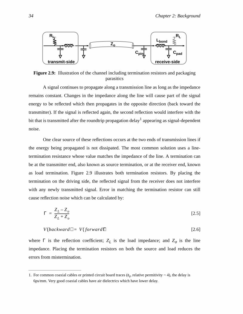
A signal continues to propagate along a transmission line as long as the impedance
remains constant. Changes in the impedance along the line will cause part of the signal
energy to be reflected which then propagates in the opposite direction (back toward the
transmitter). If the signal is reflected again, the second reflection would interfere with the
bit that is transmitted after the roundtrip propagation delay1 appearing as signal-dependent
noise.
One clear source of these reflections occurs at the two ends of transmission lines if
the energy being propagated is not dissipated. The most common solution uses a line-
termination resistance whose value matches the impedance of the line. A termination can
be at the transmitter end, also known as source termination, or at the receiver end, known
as load termination. Figure 2.9 illustrates both termination resistors. By placing the
termination on the driving side, the reflected signal from the receiver does not interfere
with any newly transmitted signal. Error in matching the termination resistor can still
cause reflection noise which can be calculated by:
[2.5]
[2.6]
where Γ is the reflection coefficient;ZL is the load impedance; andZo is the line
impedance. Placing the termination resistors on both the source and load reduces the
errors from mistermination.
1. For common coaxial cables or printed circuit board traces (εr, relative permitivity ~ 4), the delay is
6ps/mm. Very good coaxial cables have air dielectrics which have lower delay.
Figure 2.9: Illustration of the channel including termination resistors and packagingparasitics
Zo
receive-side
RL
transmit-side
RL
Cpad
Lbond
Cpin
ΓZL Zo–
ZL Zo+-------------------=
V backward( ) V forward( )Γ=
2.3 Example of a Basic Link 35
Besides the inaccurate termination, common sources of impedance mismatch are
discontinuities in the channel such as the chip packaging, connectors, and PCB trace
stubs. For example, in chip packages, a signal is often further separated from its return
path causing a higher inductance (higher impedance) and hence an impedance mismatch.
Since the length of this higher-impedance segment is often less than the wavelength of the
maximum frequency propagated on the line, the segment can be modeled as a lumped
inductance. Parasitic shunt capacitances can also be present at the pins and pads of the
chip package. Figure 2.9 illustrates both these parasitic elements. Because the impedance
of these reactive elements varies with frequency, signals containing high frequencies are
subject to more noise due to more severe mismatch.
Another source related to the impedance discontinuities is the coupling between
two signals commonly in chip packages or connectors because the return current of a
signal is flowing through another signal instead of the reference. This coupling noise,
known as crosstalk, is often modeled as mutual inductance or capacitance between the
signal wires. To reduce the effect of this induced noise, conservative designs can minimize
the interference by physically and electrically isolating the transmitted and received
signals from other signals, and properly shielding the signal. Note that for noise due to
coupling to affect differential signals, the amount of coupling must be different to the
differential lines.
These noise sources are the primary types of noise that the transmitter and receive
must deal with. The following sections discuss each of the electronic components in a link
beginning with the transmitter.
2.3.2 TransmitterThe transmitter drives aHIGH or LOW analog voltage onto the channel and is designed
for a particular output-voltage swing as determined by the system specification. The
design criteria are primarily to maintain small voltage noise and timing noise on the
signal. Transmitter bandwidth is typically not an issue for the simple links because the low
transmission-line impedance allows very high bandwidths even with significant output
capacitance. This section describes the design of typical transmitters.
36 Chapter 2: Background
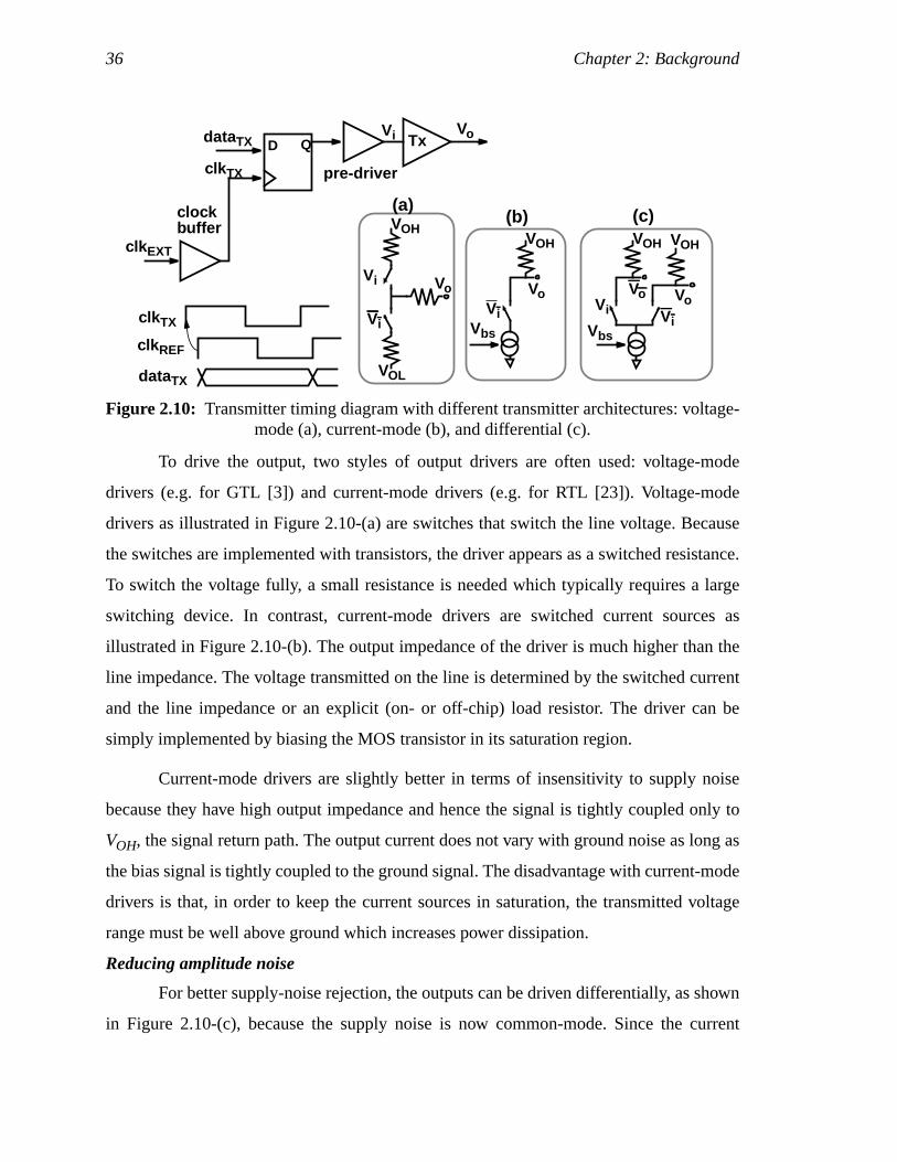
To drive the output, two styles of output drivers are often used: voltage-mode
drivers (e.g. for GTL [3]) and current-mode drivers (e.g. for RTL [23]). Voltage-mode
drivers as illustrated in Figure 2.10-(a) are switches that switch the line voltage. Because
the switches are implemented with transistors, the driver appears as a switched resistance.
To switch the voltage fully, a small resistance is needed which typically requires a large
switching device. In contrast, current-mode drivers are switched current sources as
illustrated in Figure 2.10-(b). The output impedance of the driver is much higher than the
line impedance. The voltage transmitted on the line is determined by the switched current
and the line impedance or an explicit (on- or off-chip) load resistor. The driver can be
simply implemented by biasing the MOS transistor in its saturation region.
Current-mode drivers are slightly better in terms of insensitivity to supply noise
because they have high output impedance and hence the signal is tightly coupled only to
VOH, the signal return path. The output current does not vary with ground noise as long as
the bias signal is tightly coupled to the ground signal. The disadvantage with current-mode
drivers is that, in order to keep the current sources in saturation, the transmitted voltage
range must be well above ground which increases power dissipation.
Reducing amplitude noise
For better supply-noise rejection, the outputs can be driven differentially, as shown
in Figure 2.10-(c), because the supply noise is now common-mode. Since the current
Figure 2.10: Transmitter timing diagram with different transmitter architectures: voltage-mode (a), current-mode (b), and differential (c).
TxD QdataTX
clk TX
VOH
VOL
VOH
(c)(a)
clk TX
clk REF
dataTX
pre-driver
clockbuffer
clk EXTVOH
(b)VOH
Vbs Vbs
Vo
Vo VoVo
VoVi
Vi ViViVi
Vi
2.3 Example of a Basic Link 37
remains roughly constant, the transmitter also induces less switching noise on the supply
which could benefit other transmitted or received signals on the same die.
To reduce reflections at the end of the transmission line, the transmitter should be
designed with the proper output resistance to serve as the termination resistor placed at the
very end of the channel. An off-chip resistor could introduce significant impedance
mismatch because of the remaining stub composed of the package parasitics that is in
parallel with the resistor. To incorporate the resistor, with current-mode drivers, an explicit
on-chip resistor at the driver can act as the source termination resistor [71]. If a resistive
layer is not available, a transistor in its linear region can be used as the resistor [20]. With
voltage-mode drivers, the design is slightly more complex because the switch resistance
should match the line impedance,Zo. This may be done either through proper sizing of the
driver [21] or by oversizing the driver and compensating with an external series resistor, as
shown in the Figure 2.10-(a) [86]. Because the output impedance of the transmitter varies
with process technology variations, techniques such as one by [21] adapt the output
impedance to match the line impedance.
As mentioned in the previous section, reactive parasitics on the transmission lines,
modeled as series inductors or shunt capacitors, introduce reflected or coupled noise that
are frequency dependent: the higher the signal frequency, the worse the noise. Because the
output bandwidth is typically higher than the signalling rates, transmitters are often
designed not to drive frequencies higher than the necessary signalling rate to reduce the
signal frequencies that the channel must deal with. Many links purposely slow down the
output transition (called slew-rate control) either by using a weakened pre-driver or by
switching the driver incrementally with multiple switches that are time delayed [85].
Timing noise
Besides taking care to reduce amplitude noise, the transmitted signal must also be
carefully timed. For the data bits to occur in sequence with a fixed bit-time, the transmitter
drives data that are synchronized to the on-chip clock. Figure 2.10 shows the data latched
by clkTX before being transmitted. The transmit clock,clkTX, is the on-chip, buffered
(sometimes frequency multiplied) version of an off-chip timing reference. Transmitter
clock jitter causes variation in the bit-time which reduces the timing margin. In addition to
38 Chapter 2: Background
this jitter, the delay from the clock to the output signal is also sensitive to supply noise,
adding to the timing uncertainty. As shown in Figure 2.10, this path comprises the delay
through the clock buffers, delay through the synchronization flip-flop, and the delay of the
pre-driver and output driver. For these logic gates, supply sensitivity can be estimated by
1%-delay variation /%-supply noise which can then be used to calculate the transmitter’s
contribution to the output timing uncertainty. To reduce the degradation of the data eye
due to jitter, designers try to minimize this delay to reduce the output jitter.
Bandwidth limitation
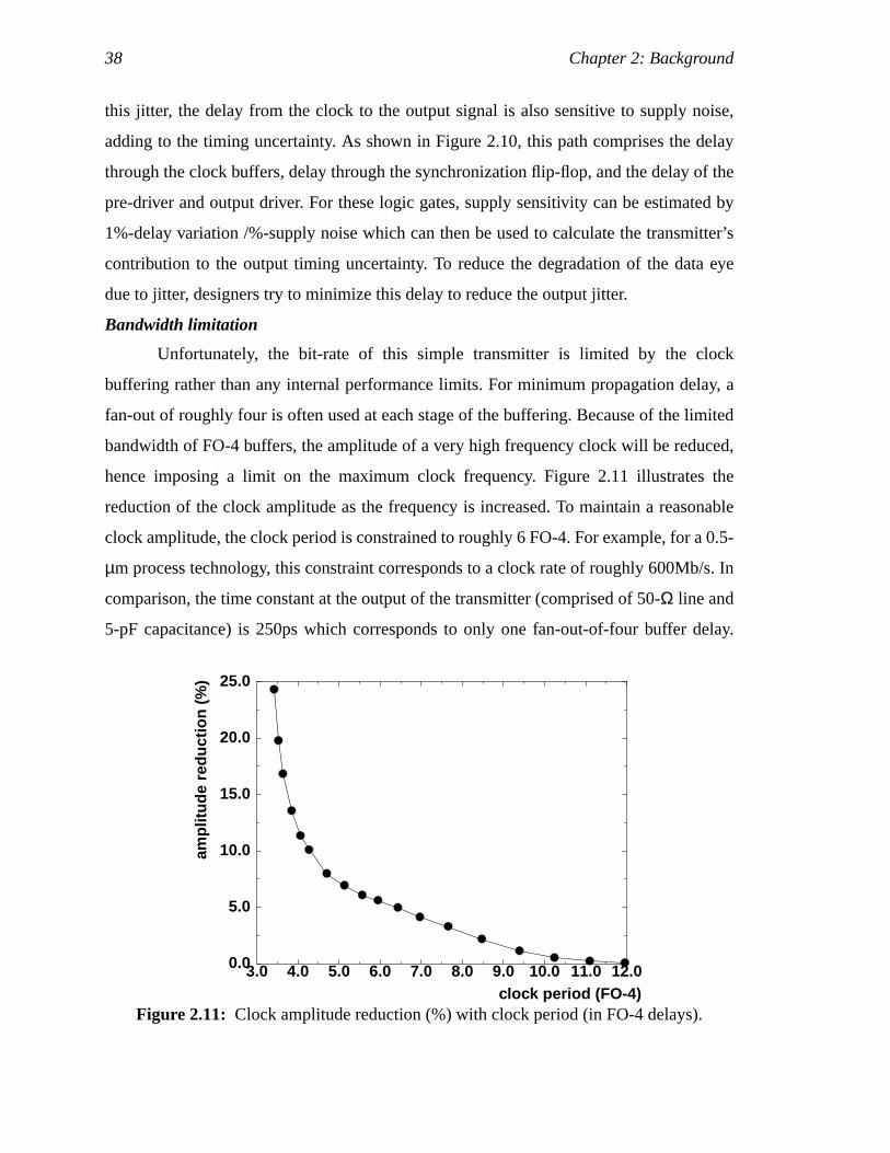
Unfortunately, the bit-rate of this simple transmitter is limited by the clock
buffering rather than any internal performance limits. For minimum propagation delay, a
fan-out of roughly four is often used at each stage of the buffering. Because of the limited
bandwidth of FO-4 buffers, the amplitude of a very high frequency clock will be reduced,
hence imposing a limit on the maximum clock frequency. Figure 2.11 illustrates the
reduction of the clock amplitude as the frequency is increased. To maintain a reasonable
clock amplitude, the clock period is constrained to roughly 6 FO-4. For example, for a 0.5-
µm process technology, this constraint corresponds to a clock rate of roughly 600Mb/s. In
comparison, the time constant at the output of the transmitter (comprised of 50-Ω line and
5-pF capacitance) is 250ps which corresponds to only one fan-out-of-four buffer delay.
Figure 2.11: Clock amplitude reduction (%) with clock period (in FO-4 delays).
3.0 4.0 5.0 6.0 7.0 8.0 9.0 10.0 11.0 12.00.0
5.0
10.0
15.0
20.0
25.0
clock period (FO-4)
ampl
itude
red
uctio
n (%
)
2.3 Example of a Basic Link 39
Often, to be practical, even the 6-FO-4 limit is not reached. In order to perform logic
processing on-chip, the clock period is often greater than 8 FO-4 to avoid excessive
pipelining, since a static flip-flop’s timing overhead (tset-up+ tclk-to-q) is roughly 3 FO-4.
2.3.3 ReceiverThe digital data is recovered from the propagated voltage waveform by two operations:
sampling the input waveform at the correct instant, and deciding the digital value of the
sampled voltage. The data waveform is sampled periodically by a clock. The timing
recovery circuit, which will be discussed in the following section, positions the clock so
that the sampling occurs at the position with maximum timing margin. The receiver
converts the transmitted voltage to digital values. One typical implementation of a receiver
([97], [40], and [86]) uses an amplifier to amplify the small-swing signal into full-swing
digital values before being sampled by a clock.
The two primary goals in the receiver design are high data bandwidth and high
resolution. The bandwidth of the amplifier determines the rate at which data can be
received. If the amplifier bandwidth is too low for the data rate, the amplifier behaves as a
filter and distorts the data, causing the wrong values to be received. The resolution
determines the minimum input voltage that can be detected. This section begins by
discussing the two issues in further detail, followed by describing receiver
implementations.
Bandwidth and resolution limitation
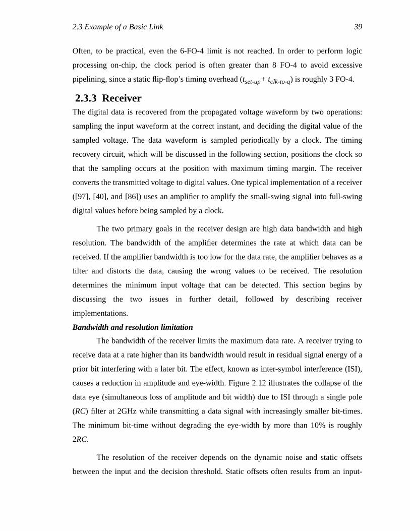
The bandwidth of the receiver limits the maximum data rate. A receiver trying to
receive data at a rate higher than its bandwidth would result in residual signal energy of a
prior bit interfering with a later bit. The effect, known as inter-symbol interference (ISI),
causes a reduction in amplitude and eye-width. Figure 2.12 illustrates the collapse of the
data eye (simultaneous loss of amplitude and bit width) due to ISI through a single pole
(RC) filter at 2GHz while transmitting a data signal with increasingly smaller bit-times.
The minimum bit-time without degrading the eye-width by more than 10% is roughly
2RC.
The resolution of the receiver depends on the dynamic noise and static offsets
between the input and the decision threshold. Static offsets often results from an input-
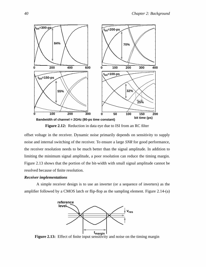
40 Chapter 2: Background
offset voltage in the receiver. Dynamic noise primarily depends on sensitivity to supply
noise and internal switching of the receiver. To ensure a largeSNR for good performance,
the receiver resolution needs to be much better than the signal amplitude. In addition to
limiting the minimum signal amplitude, a poor resolution can reduce the timing margin.
Figure 2.13 shows that the portion of the bit-width with small signal amplitude cannot be
resolved because of finite resolution.
Receiver implementations
A simple receiver design is to use an inverter (or a sequence of inverters) as the
amplifier followed by a CMOS latch or flip-flop as the sampling element. Figure 2.14-(a)
Figure 2.12: Reduction in data eye due to ISI from an RC filter
bit time (ps)0 50 100 150 2000 100 200 300
0 100 200 300 4000 200 400 600
tbit =300-ps tbit =200-ps
tbit =150-pstbit =100-ps
Bandwidth of channel = 2GHz (80-ps time constant)
84% 70%
55% 32%
25%
Figure 2.13: Effect of finite input sensitivity and noise on the timing margin
referencelevel
tmargin
vres
2.3 Example of a Basic Link 41
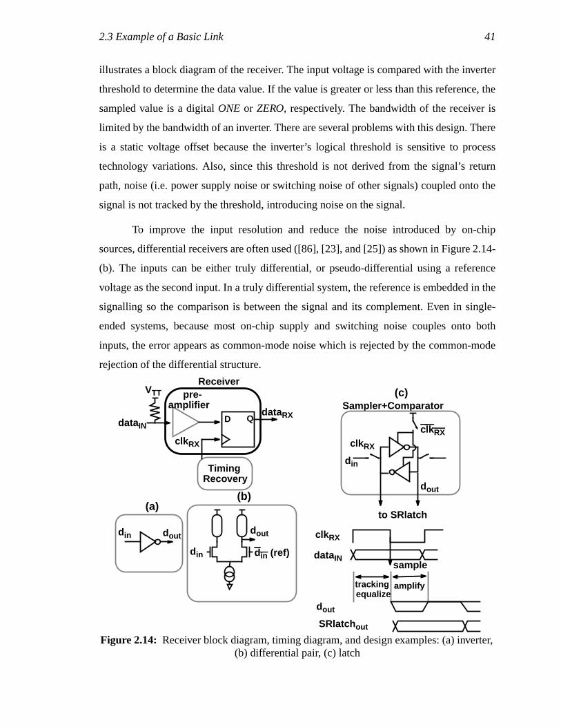
illustrates a block diagram of the receiver. The input voltage is compared with the inverter
threshold to determine the data value. If the value is greater or less than this reference, the
sampled value is a digitalONE or ZERO, respectively. The bandwidth of the receiver is
limited by the bandwidth of an inverter. There are several problems with this design. There
is a static voltage offset because the inverter’s logical threshold is sensitive to process
technology variations. Also, since this threshold is not derived from the signal’s return
path, noise (i.e. power supply noise or switching noise of other signals) coupled onto the
signal is not tracked by the threshold, introducing noise on the signal.
To improve the input resolution and reduce the noise introduced by on-chip
sources, differential receivers are often used ([86], [23], and [25]) as shown in Figure 2.14-
(b). The inputs can be either truly differential, or pseudo-differential using a reference
voltage as the second input. In a truly differential system, the reference is embedded in the
signalling so the comparison is between the signal and its complement. Even in single-
ended systems, because most on-chip supply and switching noise couples onto both
inputs, the error appears as common-mode noise which is rejected by the common-mode
rejection of the differential structure.
Figure 2.14: Receiver block diagram, timing diagram, and design examples: (a) inverter,(b) differential pair, (c) latch
dataRXSampler+Comparator
pre-amplifier
VTT (c)
clk RX
data IN
tracking
TimingRecovery
dout
D Qdata IN
clk RX
clkRXclk RX
din din (ref)
(b)(a)
din
doutdin dout
dout
to SRlatch
equalizeamplify
sample
SRlatch out
Receiver
42 Chapter 2: Background
The primary resolution limitation of this circuit is the mismatches between the
differential input transistors (VT or KP of devices as discussed by Pelgrom in [76] and
Mizuno in [69]) which can cause an input-offset voltage. This offset voltage can limit the
input resolution to tens of millivolts.1 As discussed in Section 2.2.1, this offset impacts the
performance of the link by reducing the effective signal amplitude. For an optical link, Hu
in [39] improves on the voltage resolution of receivers to roughly 6mV by using an input
offset-cancellation scheme that stores the offset voltage on capacitors and uses the stored
voltage to subtract the offset from the input amplifiers. The bandwidth of this type of
receiver is the bandwidth of the differential amplifier. For a gain of 4 per stage, the bit-
time is limited to roughly 4 FO-4 for less than 10% ISI. Multiple stages are often used for
sufficient gain as shown in [39].
An alternative receiver design, used in this dissertation, is to use a very sensitive
comparator following an analog sampling instead of amplifying prior to the sampling.
These receivers operate with two phases of operation. In the first phase, the sampler tracks
the input while the amplifier equalizes its outputs. In the second phase, the sampler holds
the last input voltage while the comparator amplifies and resolves.2 A similar variant
combines the sampling and comparing by using a comparator switched by the clock signal
([28] and [40]). An example of this method is shown in Figure 2.14-(c) along with the
timing diagram of its operation. To regenerate the signal, the comparator uses positive
feedback where the voltage gain is exponentially related to the time given to amplify.
Therefore, since the comparator is equalized prior to amplifying, a higher bit-rate does not
cause ISI. Typically, an SR-latch follows the comparator to remove the equalization phase
from the signal presented to the logic.
One disadvantage of the sampling technique is that it introduces sampling noise,
kT/C. This is in addition to the thermal noise of the termination resistor and of the CMOS
devices,α4kTf/gm (whereα is an adjustment factor). Fortunately, these noise magnitudes
1. The amount of device mismatch depends on the device size [76] and increases with scaling.
2. Often three phases are used where the sampler performs sample, hold, and track, while thecomparator, performs offset cancellation, amplification, and reset.
2.3 Example of a Basic Link 43
are typically less than a few hundred microvolts even for several gigahertz bandwidths,
and are not a significant factor for electrical systems with large voltage swings.
Similar to the prior topology, the switched comparator still has an input-offset
voltage due toVT andKP mismatches. The offset voltage can be cancelled in a similar
manner as that of the differential pair.1 In order to guarantee sufficient voltage swing at the
output of the comparator, the bit-time is limited by the sum of the regeneration time and
the equalization time. The minimum time to amplify a small input (of several tens of
millivolts) is the time required for the positive feedback to regenerate to the desired
voltage swing for the following stage. For small input voltage swing, high gain (as high as
100 in a design by Hu [39]) may be necessary to convert the input waveform into digital
values. To resolve an input difference of 10mV, a regeneration time of 3 FO-4 is often
necessary. Since a typical comparator amplifies for a half cycle and equalizes the second
half cycle, the bit-time is roughly 6 FO-4. Notice that because of the equalization phase,
the actual cycle-time of this type of receiver is not better than the bit-time limitation of
cascaded differential amplifiers. However, as will be demonstrated in the next section, the
cycle-time of the comparator can be decoupled from the sampling rate of the input
allowing higher data rates without increasing the cycle-time of the comparator.
Interestingly, the bit-time limit of the sampler+comparator receiver is similar to the
transmitter bit-time limit due to the minimum clock rate. As long as receiver timing errors
do not significantly reduce the timing margin, 6 FO-4 is the bit-time limit for this simple
architecture.
2.3.4 Timing recoveryFor maximum timing margin, the receiver should sample the bits in the middle of the data
eye. The performance of the link is affected by how well the clock edge is positioned with
respect to the incoming data stream. This clock position must be determined from the
phase and frequency of incoming data by the timing recovery circuit. The first part of this
section illustrates how the timing information is propagated from the transmitter to the
1. As will be discussed in Chapter 3, the design in this dissertation attempts to maintain a low offset butdoes not actively cancel the offset because the resolution of tens of millivolts that these circuitsachieve is sufficient for chip-to-chip links with large signal amplitude.
44 Chapter 2: Background
receiver. The second part describes two different approaches to timing recovery. The first
and most common is a phase-locked loop (PLL) which uses a feedback loop to detect and
adjust the sampling clock position. The second is oversampled phase-picking which
chooses the correct data from an oversampling of the input stream. Trade-offs and
comparison between the two architectures will be explored in a Chapter 4. The section
concludes by discussing timing errors in a simple link.
Synchronization between transmitter and receiver
The timing relationship between the transmitter and receiver depends on the
system design. Many smaller systems derive the clock for all components from a single
clock source (crystal oscillator). While the frequency is the same, the phases of the clocks
are not the same (known as a mesochronous system in [68]). For many serial links
(typically for larger systems), the transmitter and receiver have separate clock sources that
have "nominally" but not exactly the same frequency (known as a plesiochronous system
in [68]). In this case, the receiving system must not only acquire bit timing but also
additional byte synchronization to handle the frequency offsets. The latter task, although
important, is not addressed as part of the timing recovery. (Section 4.4 will describe how
the frequency offset is handled in the specific design of this dissertation.) The timing
recovery focuses on the proper positioning of the sampling clock in a bit based on phase
information in the data.
In order for the receiver to recover the phase information from the transmitted data,
the information must be communicated from the transmitter to the receiver. For links that
have multiple interconnections (parallel links), source-synchronous clocking is typically
used where the transmitter clock,clkTX, is transmitted on a parallel connection with a
delay properly matched with the data to maintain the timing relationship ofclkREF with
dataTX ([49], [51], [68], and [86]). The timing relationship is shown in the timing diagram
at the bottom of Figure 2.10. This type of connection is typically used when the cost of the
channel and the pins is small so that the multiple interconnections can be afforded. In
contrast, when the cost of the signalling medium is high due to the distance or the
necessary bandwidth, serial connections are used which embed or encode the phase
information in the signal. The phase information is guaranteed typically by encoding data
transitions in the signal stream. For very high data rates, the matching of an external clock
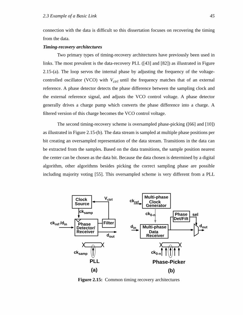
2.3 Example of a Basic Link 45
connection with the data is difficult so this dissertation focuses on recovering the timing
from the data.
Timing-recovery architectures
Two primary types of timing-recovery architectures have previously been used in
links. The most prevalent is the data-recovery PLL ([43] and [82]) as illustrated in Figure
2.15-(a). The loop servos the internal phase by adjusting the frequency of the voltage-
controlled oscillator (VCO) withVctrl until the frequency matches that of an external
reference. A phase detector detects the phase difference between the sampling clock and
the external reference signal, and adjusts the VCO control voltage. A phase detector
generally drives a charge pump which converts the phase difference into a charge. A
filtered version of this charge becomes the VCO control voltage.
The second timing-recovery scheme is oversampled phase-picking ([66] and [10])
as illustrated in Figure 2.15-(b). The data stream is sampled at multiple phase positions per
bit creating an oversampled representation of the data stream. Transitions in the data can
be extracted from the samples. Based on the data transitions, the sample position nearest
the center can be chosen as the data bit. Because the data chosen is determined by a digital
algorithm, other algorithms besides picking the correct sampling phase are possible
including majority voting [55]. This oversampled scheme is very different from a PLL
Figure 2.15: Common timing recovery architectures
PhaseDetector/
ClockSource
Filter
cksamp
doutReceiver
Vctrl
PLL
ckref /din
(a) (b)
PhaseDet/Filt
ClockGenerator
DataReceiver
ck0-n
din
ck ref
Multi-phase
sel
dout
Multi-phase
Phase-Picker
ck0-ncksamp
46 Chapter 2: Background
because it contains no inherent feedback. The need to oversample the data has made this
approach more common in lower-speed links.
Timing errors in a PLL
To maintain good timing margin, both static and dynamic phase errors must be
minimized. Ideally, a PLL maintains zero static phase error by servoing the phase based
on the phase detector and charge pump output. However, static phase errors are introduced
by mismatches in these loop elements. For example, a phase detector could detect the
phase difference by aligning the transitions of data with the rising edge of the clock and
then sample the data with the falling edge. One possible cause of static phase offset would
be if the duty-cycle of the clock is not 50%, causing the falling edge to not sample at the
middle of the data eye. Errors in the charge pump also introduce phase offsets. For
example, a mismatch in the charge pump could result in non-zero net charge when phases
are aligned causing the control voltage of the VCO to change; a phase offset would result
to compensate. Careful designs correct for these errors with active feedback as shown by
Maneatis in [63] who demonstrated a static phase offset of roughly 25ps.
Dynamic phase error also poses a significant penalty on the timing margin. The
error is often introduced by the jitter in the VCO of the PLL. Although there is a small
thermal noise component to jitter, jitter depends primarily on the sensitivity of these
elements to on-chip noise. Since links often reside on chips that have significant digital
switching, supply noise causes delay variation in ring-oscillator elements and clock
buffers.1 The timing-recovery circuit allows the sampling clock to track some of the phase
movements of the reference which reduces the timing error. The finite bandwidth of the
loop limits this tracking. The magnitude of the resulting jitter depends on the amount of
supply noise and whether the supply noise can be tracked or rejected. Designers of PLLs
have demonstrated peak-to-peak jitter of less than 1 FO-4 delay ([104], [56] and [64])
even in noisy environments. Consequently, the effective timing margin can be as large as 2
1. The jitter accumulates in an oscillator. A common variation for systems where clock and data are thesame frequency is to use a voltage-controlled delay-line (VCDL) instead of a VCO [47] to avoid theaccumulation.
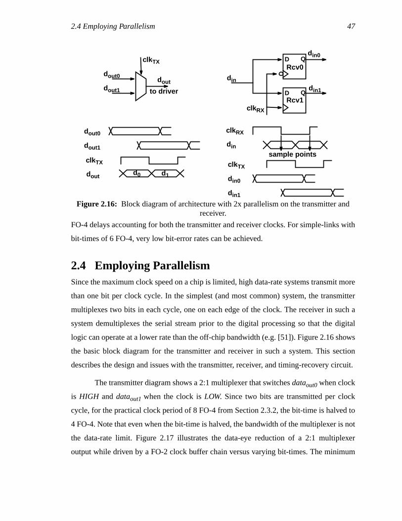
2.4 Employing Parallelism 47
FO-4 delays accounting for both the transmitter and receiver clocks. For simple-links with
bit-times of 6 FO-4, very low bit-error rates can be achieved.
2.4 Employing ParallelismSince the maximum clock speed on a chip is limited, high data-rate systems transmit more
than one bit per clock cycle. In the simplest (and most common) system, the transmitter
multiplexes two bits in each cycle, one on each edge of the clock. The receiver in such a
system demultiplexes the serial stream prior to the digital processing so that the digital
logic can operate at a lower rate than the off-chip bandwidth (e.g. [51]). Figure 2.16 shows
the basic block diagram for the transmitter and receiver in such a system. This section
describes the design and issues with the transmitter, receiver, and timing-recovery circuit.
The transmitter diagram shows a 2:1 multiplexer that switchesdataout0 when clock
is HIGH anddataout1 when the clock isLOW. Since two bits are transmitted per clock
cycle, for the practical clock period of 8 FO-4 from Section 2.3.2, the bit-time is halved to
4 FO-4. Note that even when the bit-time is halved, the bandwidth of the multiplexer is not
the data-rate limit. Figure 2.17 illustrates the data-eye reduction of a 2:1 multiplexer
output while driven by a FO-2 clock buffer chain versus varying bit-times. The minimum
Figure 2.16: Block diagram of architecture with 2x parallelism on the transmitter andreceiver.
clk RX
dinsample points
din0
clk TX
dout0
dout1 to driver D Q
D Q
dindin1
din0
Rcv0
Rcv1clk RX
din1
clk TX
dout
dout0
dout1
dout
d0 d1
clk TX
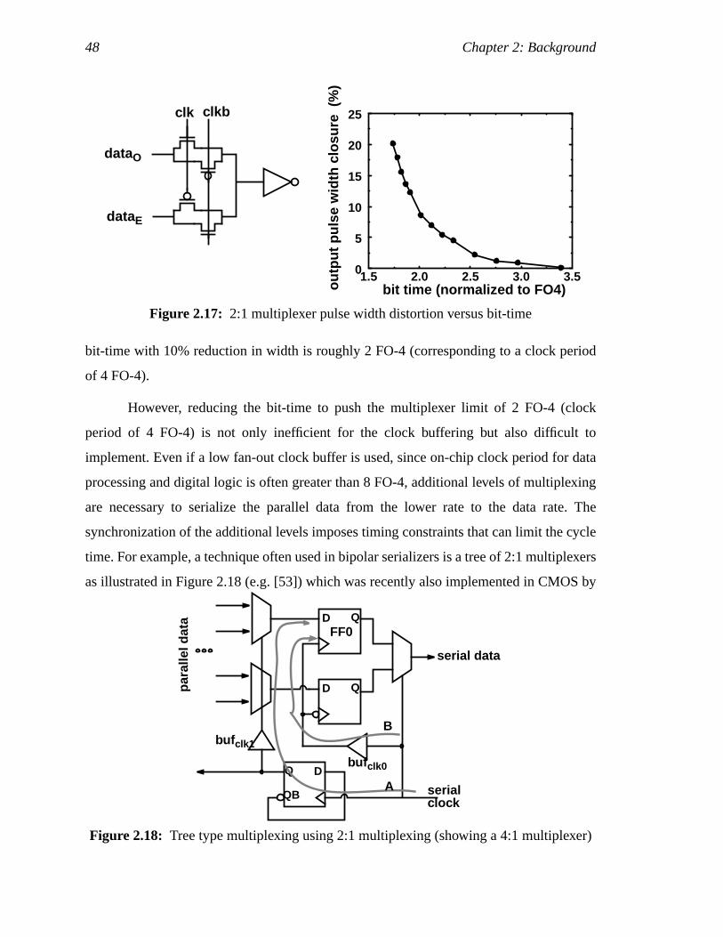
48 Chapter 2: Background
bit-time with 10% reduction in width is roughly 2 FO-4 (corresponding to a clock period
of 4 FO-4).
However, reducing the bit-time to push the multiplexer limit of 2 FO-4 (clock
period of 4 FO-4) is not only inefficient for the clock buffering but also difficult to
implement. Even if a low fan-out clock buffer is used, since on-chip clock period for data
processing and digital logic is often greater than 8 FO-4, additional levels of multiplexing
are necessary to serialize the parallel data from the lower rate to the data rate. The
synchronization of the additional levels imposes timing constraints that can limit the cycle
time. For example, a technique often used in bipolar serializers is a tree of 2:1 multiplexers
as illustrated in Figure 2.18 (e.g. [53]) which was recently also implemented in CMOS by
Figure 2.17: 2:1 multiplexer pulse width distortion versus bit-time
dataO
dataE
bit time (normalized to FO4)outp
ut p
ulse
wid
th c
losu
re (
%)
clk clkb
1.5 2.0 2.5 3.0 3.50
5
10
15
20
25
Figure 2.18: Tree type multiplexing using 2:1 multiplexing (showing a 4:1 multiplexer)
D Q
para
llel d
ata
serial data
D Q
DQ
QB serialclock
buf clk0
buf clk1
A
B
FF0
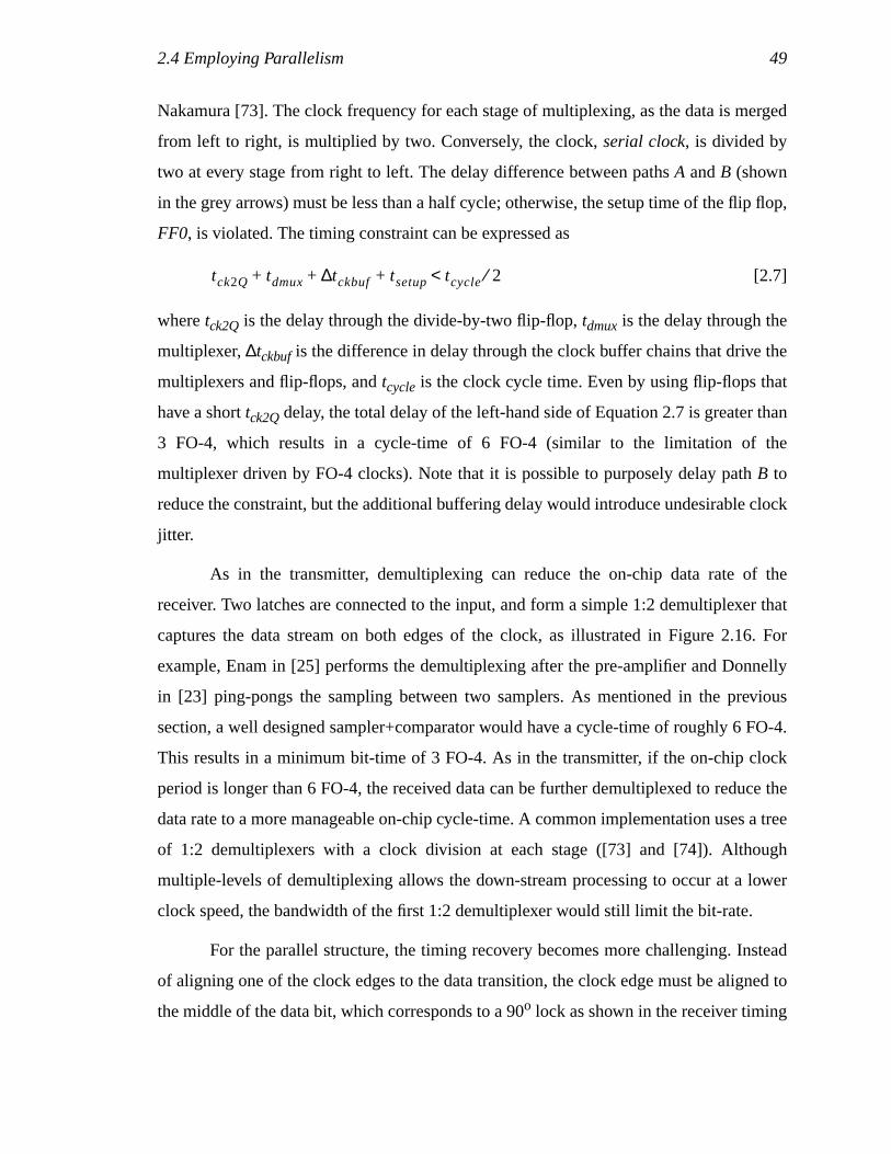
2.4 Employing Parallelism 49
Nakamura [73]. The clock frequency for each stage of multiplexing, as the data is merged
from left to right, is multiplied by two. Conversely, the clock,serial clock, is divided by
two at every stage from right to left. The delay difference between pathsA andB (shown
in the grey arrows) must be less than a half cycle; otherwise, the setup time of the flip flop,
FF0, is violated. The timing constraint can be expressed as
[2.7]
wheretck2Q is the delay through the divide-by-two flip-flop,tdmux is the delay through the
multiplexer,∆tckbuf is the difference in delay through the clock buffer chains that drive the
multiplexers and flip-flops, andtcycle is the clock cycle time. Even by using flip-flops that
have a shorttck2Q delay, the total delay of the left-hand side of Equation 2.7 is greater than
3 FO-4, which results in a cycle-time of 6 FO-4 (similar to the limitation of the
multiplexer driven by FO-4 clocks). Note that it is possible to purposely delay pathB to
reduce the constraint, but the additional buffering delay would introduce undesirable clock
jitter.
As in the transmitter, demultiplexing can reduce the on-chip data rate of the
receiver. Two latches are connected to the input, and form a simple 1:2 demultiplexer that
captures the data stream on both edges of the clock, as illustrated in Figure 2.16. For
example, Enam in [25] performs the demultiplexing after the pre-amplifier and Donnelly
in [23] ping-pongs the sampling between two samplers. As mentioned in the previous
section, a well designed sampler+comparator would have a cycle-time of roughly 6 FO-4.
This results in a minimum bit-time of 3 FO-4. As in the transmitter, if the on-chip clock
period is longer than 6 FO-4, the received data can be further demultiplexed to reduce the
data rate to a more manageable on-chip cycle-time. A common implementation uses a tree
of 1:2 demultiplexers with a clock division at each stage ([73] and [74]). Although
multiple-levels of demultiplexing allows the down-stream processing to occur at a lower
clock speed, the bandwidth of the first 1:2 demultiplexer would still limit the bit-rate.
For the parallel structure, the timing recovery becomes more challenging. Instead
of aligning one of the clock edges to the data transition, the clock edge must be aligned to
the middle of the data bit, which corresponds to a 90o lock as shown in the receiver timing
tck2Q tdmux tckbuf∆ tsetup+ + + tcycle 2⁄<
50 Chapter 2: Background
diagram of Figure 2.16. Enam in [25] multiplies the clock frequency by two and then
apply the techniques in a simple non-demultiplexed link to avoid the problem but the
performance of the higher frequency clock will limit the system performance. For better
performance many systems either use a quadrature phase detector [32] or oversamples the
data. These techniques will be discussed in more detail in Chapter 4.
The same difficulties as in the simple link still apply in maintaining small static
and dynamic phase errors. Since the data rate is now twice the clock rate, the impact of
jitter is doubled as a percentage of the bit-time. In addition, since both rising and falling
edges of the clock are used to transmit data, a duty-cycle error can further affect
performance. A transmitter clock with duty-cycle error causes unequal bit-widths for the
odd and even data bits. With duty-cycle error in the receiver clock, both receivers can not
simultaneously sample at the middle of the data eye for both edges causing a static phase
offset for one or both data bits. Links that uses the 2:1 parallelism (e.g. [23]) have
maintained low bit-error rates by using low-jitter timing-recovery circuits and additional
circuits that perform duty-cycle correction.
2.5 SummaryThis chapter discussed the basic metrics of link performance, the data rate and the bit-
error rate. A normalization metric, fan-out-of-four delay, is introduced to represent the
data bit-time in a process-technology independent metric to simplify future discussions.
The bit-error rate is related to the amount of signal and noise in the system. A link’s design
goal is to maintain sufficient voltage margin for the signal to be resolved and timing
margin for the sampling clock to reliably sample the data. Sources of errors from each of
the link components, the channel, the transmitter, and the receiver of a simple link design
that corrupt both these margins have been discussed. The discussion shows that the
maximum rate of the basic-link example has a practical limit set by the on-chip clock
period of roughly 6 FO-4 limited by the bandwidth of the clock buffer chain. To further
extend the data rate, designers employ parallelism with 2:1 multiplexing at the transmitter
and 1:2 demultiplexing at the receiver. This low-degree parallelism improves the bit-time
2.5 Summary 51
to roughly 3 FO-4. At this point, more issues emerge such as the bandwidth of the
multiplexer and the minimum cycle time of the receiver as bandwidth-limiting factors.
A natural extension to further reduce the bit-time is to increase the degree of
parallelism. The following chapter describes transmitter and receiver architecture with bit-
time of 1 FO-4. The limitations of the multiplexer and the maximum sampling rate are
examined. At the higher data rates, the noise sources have a more severe impact on
performance. Specifically, the timing errors discussed in Section 2.3.4 become a major
concern and are discussed in Chapter 4.

52 Chapter 2: Background
53
Chapter 3
Parallelized I/O Circuits
In Chapter 2, simple parallelism improved the off-chip data rate by a factor of two without
increasing the on-chip clock frequency. Further speed-up with bit-times smaller than 3 or
4 FO-4 would encounter a limit due to the minimum cycle-time of the clock buffers,
synchronization flip-flops, and sampler+comparator. An alternative, suggested at the
conclusion of the previous chapter, is to use a higher degree of parallelism. By using an
N:1 multiplexer and 1:N demultiplexer for the transmitter and receiver (see Figure 3.1),
the on-chip clock rate can be reduced to 1/N of the data rate. The on-chip frequency and
the comparator cycle-time no longer limit the data rate.
In the transmitter, a larger fan-in multiplexer can be used with each input selected
with appropriately timed pulses ([41] and [50]). However, a higher fan-in multiplexer can
be bandwidth limited by the high capacitance of the multiplexing node. The first section of
this chapter addresses how such a transmitter can improve the bit-time despite the higher
capacitance.
To apply parallelism in the receiver, multiple clock phases are used with a different
phase for each sampler+comparator, as shown in Figure 3.1-(b). Each phase of the lower
frequency clock samples a different data bit. Section 3.2 explores the factors that limit the
sampling bandwidth. Issues in the design of a receiver with good voltage resolution are
also discussed.
54 Chapter 3: Parallelized I/O Circuits
Clearly, the timing of the select pulses for the transmitter and the clock edges for
receiver are critical to properly transmitting and receiving the data bit. In this chapter,
perfectly spaced clock phases are assumed to be supplied by a multiple clock phase
generator. The actual impact of non-ideal multiple clocks phases will be discussed in
Chapter 4.
3.1 Transmitter DesignUsing a larger fan-in multiplexer to improve data rate is difficult. Even though the higher
fan-in allows greater parallelism, two performance limitations must be addressed: the
multiplexer output has greater capacitance which limits its bandwidth, and the select
signals need to be short pulses with pulse-width on the order of one bit-time.
The effect of a large fan-in, N:1 multiplexer with similar design as the 2:1
multiplexer shown in Section 2.4 is illustrated in Figure 3.2-(a). In addition to the inverter
load, the multiplexing node,A, is loaded with the capacitance of the switches which grows
with the fan-in. One source of bandwidth limitation stems from the switch resistance and
the self-loading capacitance that form an effective RC filter. Increasing fan-in increases
Figure 3.1: Higher order multiplexing, (a), and demultiplexing, (b)
ck0ck1
ck2ck
0
ck1
ck2
Din
D0 D1 D2
Dout
Dout1
x N
Dout0 Dout2
sel0sel1
(a) (b)
D0 D1 D2
sel0 sel1 sel2
x N
Multiplexer DemultiplexerDin1Din0 Din2
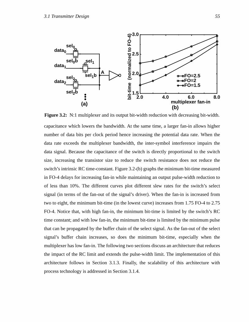
3.1 Transmitter Design 55
capacitance which lowers the bandwidth. At the same time, a larger fan-in allows higher
number of data bits per clock period hence increasing the potential data rate. When the
data rate exceeds the multiplexer bandwidth, the inter-symbol interference impairs the
data signal. Because the capacitance of the switch is directly proportional to the switch
size, increasing the transistor size to reduce the switch resistance does not reduce the
switch’s intrinsic RC time-constant. Figure 3.2-(b) graphs the minimum bit-time measured
in FO-4 delays for increasing fan-in while maintaining an output pulse-width reduction to
of less than 10%. The different curves plot different slew rates for the switch’s select
signal (in terms of the fan-out of the signal’s driver). When the fan-in is increased from
two to eight, the minimum bit-time (in the lowest curve) increases from 1.75 FO-4 to 2.75
FO-4. Notice that, with high fan-in, the minimum bit-time is limited by the switch’s RC
time constant; and with low fan-in, the minimum bit-time is limited by the minimum pulse
that can be propagated by the buffer chain of the select signal. As the fan-out of the select
signal’s buffer chain increases, so does the minimum bit-time, especially when the
multiplexer has low fan-in. The following two sections discuss an architecture that reduces
the impact of the RC limit and extends the pulse-width limit. The implementation of this
architecture follows in Section 3.1.3. Finally, the scalability of this architecture with
process technology is addressed in Section 3.1.4.
Figure 3.2: N:1 multiplexer and its output bit-width reduction with decreasing bit-width.
data0
data1
multiplexer fan-in
bit-
time
(no
rmal
ized
to F
O-4
)
sel0
sel0b sel1
sel1bdata2
sel2
sel2b
(a)(b)
2.0 4.0 6.0 8.01.5
2.0
2.5
3.0
FO=2.5FO=2FO=1.5
A
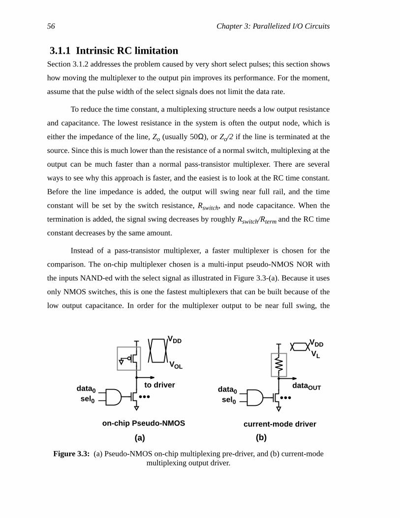
56 Chapter 3: Parallelized I/O Circuits
3.1.1 Intrinsic RC limitationSection 3.1.2 addresses the problem caused by very short select pulses; this section shows
how moving the multiplexer to the output pin improves its performance. For the moment,
assume that the pulse width of the select signals does not limit the data rate.
To reduce the time constant, a multiplexing structure needs a low output resistance
and capacitance. The lowest resistance in the system is often the output node, which is
either the impedance of the line,Zo (usually 50Ω), or Zo/2 if the line is terminated at the
source. Since this is much lower than the resistance of a normal switch, multiplexing at the
output can be much faster than a normal pass-transistor multiplexer. There are several
ways to see why this approach is faster, and the easiest is to look at the RC time constant.
Before the line impedance is added, the output will swing near full rail, and the time
constant will be set by the switch resistance,Rswitch, and node capacitance. When the
termination is added, the signal swing decreases by roughlyRswitch/Rtermand the RC time
constant decreases by the same amount.
Instead of a pass-transistor multiplexer, a faster multiplexer is chosen for the
comparison. The on-chip multiplexer chosen is a multi-input pseudo-NMOS NOR with
the inputs NAND-ed with the select signal as illustrated in Figure 3.3-(a). Because it uses
only NMOS switches, this is one the fastest multiplexers that can be built because of the
low output capacitance. In order for the multiplexer output to be near full swing, the
Figure 3.3: (a) Pseudo-NMOS on-chip multiplexing pre-driver, and (b) current-modemultiplexing output driver.
dataOUT
VDD
VOL
to driverdata0
VDD
VL
(a) (b)
on-chip Pseudo-NMOS current-mode driver
sel0data0sel0
3.1 Transmitter Design 57
NMOS switch must pull the output voltage to be lower thanVT, which means that the
switch resistance must be ratioed lower than the load resistance.
If the multiplexing is performed at the output, the same output structure behaves as
a current-mode driver, shown in Figure 3.3-(b). As long as the NMOS transistors stay in
saturation, the devices appear as high-impedance current sources. The output resistance is
dominated by the impedance of the channel, and the output capacitance is dominated by
the output-device parasitics. This capacitance depends on the device size which in turn
depends on the output current.
With a current-mode driver, a reasonable swing of 500mV would require 20mA of
output current in a doubly terminated (25-Ω) environment. Reasonably process
independent metrics can be used to estimate the necessary device size and capacitance to
drive such current. NMOS transistors have source and drain capacitance of roughly 2fF/
µm of transistor width and have a saturation current,IDSAT, of roughly 400µA/µm of
transistor width1. Using these metrics, the drain capacitance of the output transistor (CD),
in a 0.5-µm process technology, is roughly 100fF for each NMOS switched current source
to switch the 20-mA current. For a fair comparison of the data rate with an on-chip
multiplexer, assume that the pseudo-NMOS multiplexer drives a comparable output
resistance. The NMOS switch must then be considerably larger to drive the output fully
LOW. The switch resistance must be less than 1/3 the load resistance for an output low
voltage less thanVT. For a 3.3-V supply, the voltage swing is 5x2 larger than that of the
current-mode driver, and the capacitance per switch is roughly 4*CD per transistor
resulting in a 4x reduction in data rate.
The minimum bit-time of the current-mode multiplexing (based on the 2RC
estimate from Section 2.4) is roughly
NCDZo seconds [3.1]
1. The IDSAT metric assumes idealized scaling of supply voltage and threshold voltage. The
technology related numbers roughly corresponds to all three of the processes used in this research arewithin 25% error.
2. Because a PMOS is used as the pull up resistance, the resistance depends on the output voltage. Theswitch size does not need to be 5x larger for a 5x increase in voltage swing.
58 Chapter 3: Parallelized I/O Circuits
whereN is the fan-in (or the number ofCD) and the output impedance isZo/2. However,
capacitance in addition toCD that are present at the output will increase this minimum bit-
time. The two primary sources are the capacitance associated with the load resistor and
parasitic capacitance at the output pad.
The capacitance of the load device depends on the implementation. In some
process technologies, an accurate resistor layer with low capacitance is available so the
extra capacitance can be reduced. Otherwise, a PMOS transistor, biased in its linear
region, can be used instead of the resistor1, as shown in Figure 3.3-(a), which is typical of
a pseudo-NMOS logic circuit. The device size required for a 50-Ω PMOS resistor
contributes roughly 3*CD of output capacitance, or roughly 300fF in the 0.5-µm process
technology. The bit-time penalty due to this capacitance depends on the fan-in of the
multiplexer. With large fan-ins such as eight, the penalty is amortized to increase the bit-
time by only 35%.
Parasitic capacitances further increase the minimum bit-time. These parasitics
such as the on-chip bonding-pad capacitance, ESD device capacitance, and package-
related capacitance are non-device-related and introduce a fixed penalty that is not
dependent onCD. By using smaller, rounded bonding pads, eliminating the ESD device,
and using good packaging, these capacitances can be as small as 250fF. This added
capacitance has only modest impact for a multiplexer with high fan-in. For example, the
parasitic capacitance is less than 25% of the total capacitance for an 8:1 multiplexer.2
To summarize, the minimum bit-time when considering the additional
capacitances is roughly
[(N+3)CD+Cpad]Zo sec [3.2]
1. Alternative termination schemes can lower the output capacitance. If the signal output is differential,differential termination between the outputs can be used allowing the resistance to be 100Ω. If aninaccurate resistor layer is available, a linear PMOS device can be place in parallel so that the devicedoes not need to be large to adjust the resistance.
2. Note that even if the first scenario applies, since the output driver is capable of higher data bandwidthin the absence of the additional capacitance, techniques to extend the bandwidth exist. Since thebandwidth limitation of the capacitance appears as a filter, the transmitter can pre-distort thetransmitted signal to equalize the filter [89]. Ultimately, the data rate is limited by the inherentdevice-related capacitance of the output driver.
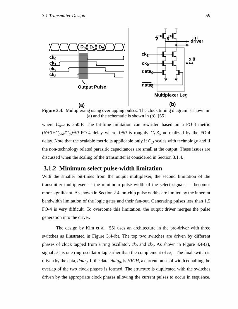
3.1 Transmitter Design 59
where Cpad is 250fF. The bit-time limitation can rewritten based on a FO-4 metric
(N+3+Cpad/CD)/50 FO-4 delay where1/50 is roughly CDZo normalized by the FO-4
delay. Note that the scalable metric is applicable only ifCD scales with technology and if
the non-technology related parasitic capacitances are small at the output. These issues are
discussed when the scaling of the transmitter is considered in Section 3.1.4.
3.1.2 Minimum select pulse-width limitationWith the smaller bit-times from the output multiplexer, the second limitation of the
transmitter multiplexer — the minimum pulse width of the select signals — becomes
more significant. As shown in Section 2.4, on-chip pulse widths are limited by the inherent
bandwidth limitation of the logic gates and their fan-out. Generating pulses less than 1.5
FO-4 is very difficult. To overcome this limitation, the output driver merges the pulse
generation into the driver.
The design by Kim et al. [55] uses an architecture in the pre-driver with three
switches as illustrated in Figure 3.4-(b). The top two switches are driven by different
phases of clock tapped from a ring oscillator,ck0 andck3. As shown in Figure 3.4-(a),
signalck3 is one ring-oscillator tap earlier than the complement ofck0. The final switch is
driven by the data,data0. If the data,data0, isHIGH, a current pulse of width equalling the
overlap of the two clock phases is formed. The structure is duplicated with the switches
driven by the appropriate clock phases allowing the current pulses to occur in sequence.
Figure 3.4: Multiplexing using overlapping pulses. The clock timing diagram is shown in(a) and the schematic is shown in (b). [55]
to
Multiplexer Leg
x 8ck0
ck3
D0 D1 D2
ck0ck1ck2ck3
Output Pulse
data0
data0
driver
(a) (b)
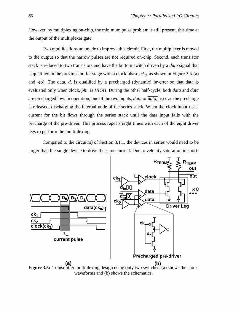
60 Chapter 3: Parallelized I/O Circuits
However, by multiplexing on-chip, the minimum pulse problem is still present, this time at
the output of the multiplexer gate.
Two modifications are made to improve this circuit. First, the multiplexer is moved
to the output so that the narrow pulses are not required on-chip. Second, each transistor
stack is reduced to two transistors and have the bottom switch driven by adata signal that
is qualified in the previous buffer stage with a clock phase,ck0, as shown in Figure 3.5-(a)
and -(b). The data,d, is qualified by a precharged (dynamic) inverter so that data is
evaluated only when clock,phi, is HIGH. During the other half-cycle, bothdata anddata
are precharged low. In operation, one of the two inputs,data or data, rises as the precharge
is released, discharging the internal node of the series stack. When the clock input rises,
current for the bit flows through the series stack until the data input falls with the
precharge of the pre-driver. This process repeats eight times with each of the eight driver
legs to perform the multiplexing.
Compared to the circuit(s) of Section 3.1.1, the devices in series would need to be
larger than the single device to drive the same current. Due to velocity saturation in short-
Figure 3.5: Transmitter multiplexing design using only two switches. (a) shows the clockwaveforms and (b) shows the schematics.
out
out
RTERM RTERM
clock
data
dataDriver Leg
x 8
ck0
din[0]
din[0]
ck3
ck
d
Precharged pre-driver
D0 D1 D2
data(ck 0)ck1ck2clock(ck 3)
current pulse
(a) (b)
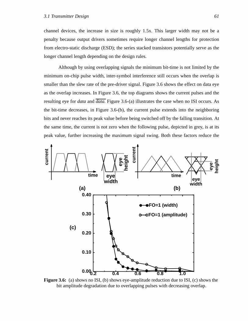
3.1 Transmitter Design 61
channel devices, the increase in size is roughly 1.5x. This larger width may not be a
penalty because output drivers sometimes require longer channel lengths for protection
from electro-static discharge (ESD); the series stacked transistors potentially serve as the
longer channel length depending on the design rules.
Although by using overlapping signals the minimum bit-time is not limited by the
minimum on-chip pulse width, inter-symbol interference still occurs when the overlap is
smaller than the slew rate of the pre-driver signal. Figure 3.6 shows the effect on data eye
as the overlap increases. In Figure 3.6, the top diagrams shows the current pulses and the
resulting eye fordata anddata. Figure 3.6-(a) illustrates the case when no ISI occurs. As
the bit-time decreases, in Figure 3.6-(b), the current pulse extends into the neighboring
bits and never reaches its peak value before being switched off by the falling transition. At
the same time, the current is not zero when the following pulse, depicted in grey, is at its
peak value, further increasing the maximum signal swing. Both these factors reduce the
Figure 3.6: (a) shows no ISI, (b) shows eye-amplitude reduction due to ISI, (c) shows thebit amplitude degradation due to overlapping pulses with decreasing overlap.
(a) (b)
time
curr
ent
eyewidth
eye
heig
ht
eyewidth
eye
heig
ht curr
ent
time
0.2 0.4 0.6 0.8 1.00.00
0.10
0.20
0.30
0.40
FO=1 (width)
FO=1 (amplitude)
(c)
62 Chapter 3: Parallelized I/O Circuits
data-eye amplitude with respect to the maximum voltage swing. Interestingly, the data
width is not affected until the tail of each current pulse extendsbeyond the neighboring bit.
To affect the pulse width, the residual current from a prior bit must interfere with the data
transition. Figure 3.6-(c) illustrates the percentage reduction in eye-amplitude and eye-
width versus the bit-time. The eye-width reduction, shown with the filled symbols,
becomes significant only after the eye-height is already heavily attenuated.
A fan-out of one buffer drives the pre-driver signal in the figure so that the signal
has a sharp transition time of 1 FO-4. Practically speaking, fan-outs less than one are
extremely inefficient because nearly half of the total capacitance is from self-loading.
Further decrease in the pre-driver fan-out would only improve the minimum bit-time
slightly while consuming excessive area and power. Based on Figure 3.6-(c), the minimum
bit-time, with pre-driver fan-out of one, is roughly 0.5 FO-4. An advantage of the
overlapping architecture is that the pre-driver’s signals are at a much lower frequency than
the data rate so only the final stage of the pre-driver chain requires the small fan-out.
Higher fan-outs can be used in the pre-driver’s buffering chain to save power without
introducing ISI.
Since the eye width degrades only at very small bit-time, this architecture can
actually push bit-times to even less than 0.5 FO-4 if the application can handle large
amplitude noise. However, the remaining discussion defines the minimum bit-time as
when the bit amplitude is degraded by 10% because the wasted signal power is often not
tolerable. Furthermore, it remains to be seen in the next chapter whether the timing
resolution of the rising and falling edges can support such low bit-times.
To summarize the two sections, two factors are considered when determining the
fan-in of the output multiplexing for maximizing the data rate: the output time constant,
and the slew-rate. Optimally, the output time constant is chosen so that the signal is
degraded by roughly the same amount as by the limited slew-rate. The minimum bit-time
due to the output time constant can be estimated based on Equation 3.1 with a slight
adjustment to account for the larger devices in the NAND structure. Accounting for both
the output RC and the pre-driver slew rate with the architecture shown in Figure 3.5,
Figure 3.7 shows the reduction of signal amplitude with varying bit-times. The lowest
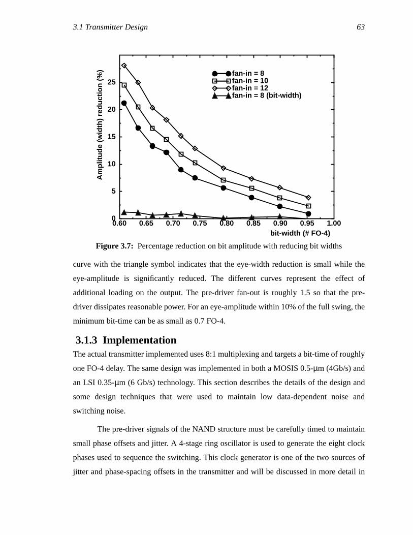
3.1 Transmitter Design 63
curve with the triangle symbol indicates that the eye-width reduction is small while the
eye-amplitude is significantly reduced. The different curves represent the effect of
additional loading on the output. The pre-driver fan-out is roughly 1.5 so that the pre-
driver dissipates reasonable power. For an eye-amplitude within 10% of the full swing, the
minimum bit-time can be as small as 0.7 FO-4.
3.1.3 ImplementationThe actual transmitter implemented uses 8:1 multiplexing and targets a bit-time of roughly
one FO-4 delay. The same design was implemented in both a MOSIS 0.5-µm (4Gb/s) and
an LSI 0.35-µm (6 Gb/s) technology. This section describes the details of the design and
some design techniques that were used to maintain low data-dependent noise and
switching noise.
The pre-driver signals of the NAND structure must be carefully timed to maintain
small phase offsets and jitter. A 4-stage ring oscillator is used to generate the eight clock
phases used to sequence the switching. This clock generator is one of the two sources of
jitter and phase-spacing offsets in the transmitter and will be discussed in more detail in
Figure 3.7: Percentage reduction on bit amplitude with reducing bit widths
0.60 0.65 0.70 0.75 0.80 0.85 0.90 0.95 1.000
5
10
15
20
25fan-in = 8fan-in = 10fan-in = 12fan-in = 8 (bit-width)
bit-width (# FO-4)
Am
plitu
de (
wid
th)
redu
ctio
n (%
)
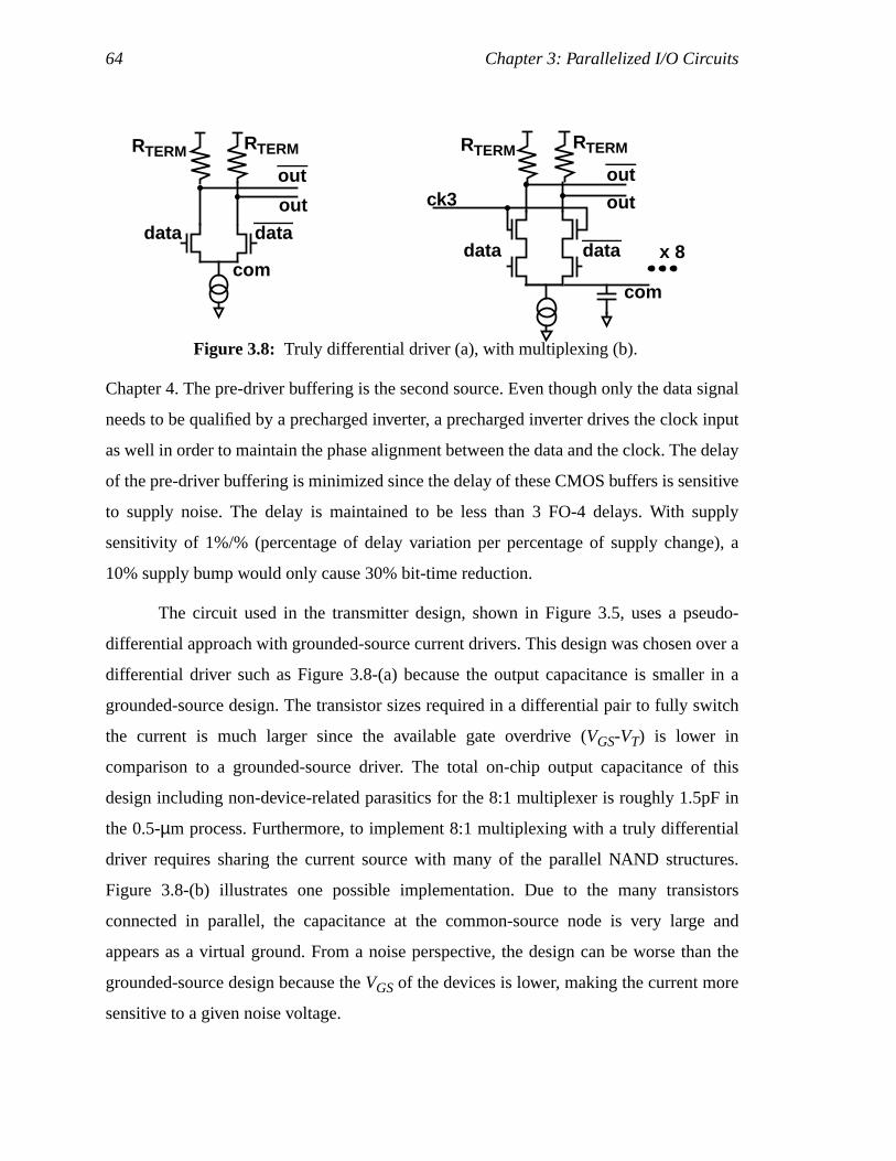
64 Chapter 3: Parallelized I/O Circuits
Chapter 4. The pre-driver buffering is the second source. Even though only the data signal
needs to be qualified by a precharged inverter, a precharged inverter drives the clock input
as well in order to maintain the phase alignment between the data and the clock. The delay
of the pre-driver buffering is minimized since the delay of these CMOS buffers is sensitive
to supply noise. The delay is maintained to be less than 3 FO-4 delays. With supply
sensitivity of 1%/% (percentage of delay variation per percentage of supply change), a
10% supply bump would only cause 30% bit-time reduction.
The circuit used in the transmitter design, shown in Figure 3.5, uses a pseudo-
differential approach with grounded-source current drivers. This design was chosen over a
differential driver such as Figure 3.8-(a) because the output capacitance is smaller in a
grounded-source design. The transistor sizes required in a differential pair to fully switch
the current is much larger since the available gate overdrive (VGS-VT) is lower in
comparison to a grounded-source driver. The total on-chip output capacitance of this
design including non-device-related parasitics for the 8:1 multiplexer is roughly 1.5pF in
the 0.5-µm process. Furthermore, to implement 8:1 multiplexing with a truly differential
driver requires sharing the current source with many of the parallel NAND structures.
Figure 3.8-(b) illustrates one possible implementation. Due to the many transistors
connected in parallel, the capacitance at the common-source node is very large and
appears as a virtual ground. From a noise perspective, the design can be worse than the
grounded-source design because theVGS of the devices is lower, making the current more
sensitive to a given noise voltage.
Figure 3.8: Truly differential driver (a), with multiplexing (b).
out
out
RTERM RTERM
x 8data data
ck3
com
data data
com
out
RTERM RTERM
out
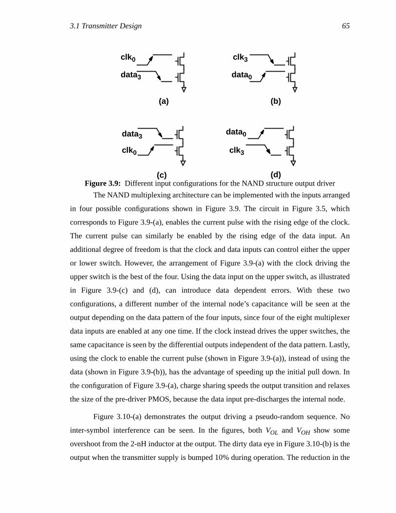
3.1 Transmitter Design 65
The NAND multiplexing architecture can be implemented with the inputs arranged
in four possible configurations shown in Figure 3.9. The circuit in Figure 3.5, which
corresponds to Figure 3.9-(a), enables the current pulse with the rising edge of the clock.
The current pulse can similarly be enabled by the rising edge of the data input. An
additional degree of freedom is that the clock and data inputs can control either the upper
or lower switch. However, the arrangement of Figure 3.9-(a) with the clock driving the
upper switch is the best of the four. Using the data input on the upper switch, as illustrated
in Figure 3.9-(c) and (d), can introduce data dependent errors. With these two
configurations, a different number of the internal node’s capacitance will be seen at the
output depending on the data pattern of the four inputs, since four of the eight multiplexer
data inputs are enabled at any one time. If the clock instead drives the upper switches, the
same capacitance is seen by the differential outputs independent of the data pattern. Lastly,
using the clock to enable the current pulse (shown in Figure 3.9-(a)), instead of using the
data (shown in Figure 3.9-(b)), has the advantage of speeding up the initial pull down. In
the configuration of Figure 3.9-(a), charge sharing speeds the output transition and relaxes
the size of the pre-driver PMOS, because the data input pre-discharges the internal node.
Figure 3.10-(a) demonstrates the output driving a pseudo-random sequence. No
inter-symbol interference can be seen. In the figures, bothVOL and VOH show some
overshoot from the 2-nH inductor at the output. The dirty data eye in Figure 3.10-(b) is the
output when the transmitter supply is bumped 10% during operation. The reduction in the
Figure 3.9: Different input configurations for the NAND structure output driver
data0
clk 3
data3
clk 0
data3
clk 0
data0
clk 3
(a) (b)
(c) (d)
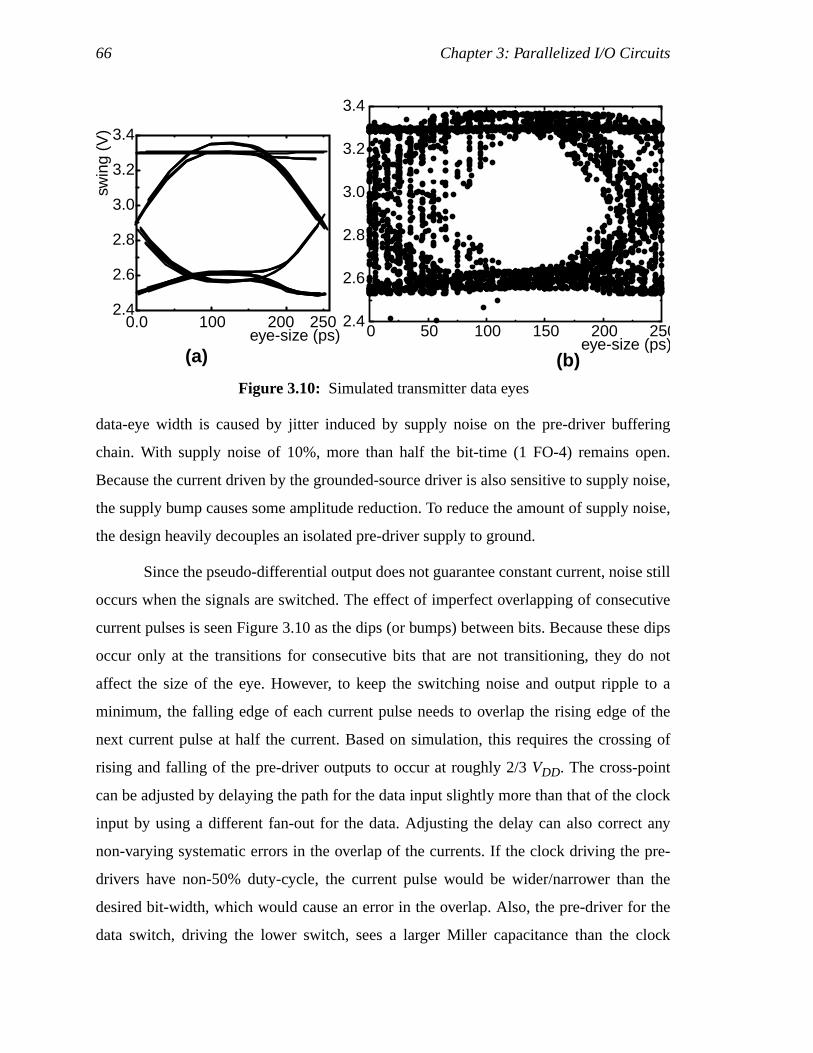
66 Chapter 3: Parallelized I/O Circuits
data-eye width is caused by jitter induced by supply noise on the pre-driver buffering
chain. With supply noise of 10%, more than half the bit-time (1 FO-4) remains open.
Because the current driven by the grounded-source driver is also sensitive to supply noise,
the supply bump causes some amplitude reduction. To reduce the amount of supply noise,
the design heavily decouples an isolated pre-driver supply to ground.
Since the pseudo-differential output does not guarantee constant current, noise still
occurs when the signals are switched. The effect of imperfect overlapping of consecutive
current pulses is seen Figure 3.10 as the dips (or bumps) between bits. Because these dips
occur only at the transitions for consecutive bits that are not transitioning, they do not
affect the size of the eye. However, to keep the switching noise and output ripple to a
minimum, the falling edge of each current pulse needs to overlap the rising edge of the
next current pulse at half the current. Based on simulation, this requires the crossing of
rising and falling of the pre-driver outputs to occur at roughly 2/3VDD. The cross-point
can be adjusted by delaying the path for the data input slightly more than that of the clock
input by using a different fan-out for the data. Adjusting the delay can also correct any
non-varying systematic errors in the overlap of the currents. If the clock driving the pre-
drivers have non-50% duty-cycle, the current pulse would be wider/narrower than the
desired bit-width, which would cause an error in the overlap. Also, the pre-driver for the
data switch, driving the lower switch, sees a larger Miller capacitance than the clock
Figure 3.10: Simulated transmitter data eyes
0.0 100 200 2502.4
2.6
2.8
3.0
3.2
3.4
eye-size (ps)
swin
g (V
)
(a)0 50 100 150 200 250
2.4
2.6
2.8
3.0
3.2
3.4
eye-size (ps)(b)
3.1 Transmitter Design 67
switch signal, which would cause additional delay in the data with respect to the clock.
Both of these can be compensated by additional adjustment of the fan-out difference
between the data and clock paths.
The output swing depends on the current pulled by the series-stacked transistors.
With the gate pulled toVDD, the current depends on the size of the device and is also
sensitive to process variations. In order to control the current, Kushiyama in [51] used
multiple driver devices that are digitally controlled to provide an adjustable pull-down
current to compensate for process variations. The design uses a less complex technique of
making the pre-driver’s supply adjustable to control the output current by adjustingVGS-
VT. Although this method is simple and requires no additional area and circuitry, it has the
disadvantage of causing the crossing of the pre-driver rising and falling signals to no
longer occur at the half-current point. The cross-point voltage,Vxp, scales roughly
proportionally with VDD; the half current point,Vixp, scales with an offset,
.1
Because the design is pushing the maximum data rate, the transmitter design does
not include the slew-rate control that is typical for lower data-rate links. The slew rate is
often designed to be approximately 1/3 of the bit-time in order to keep low the switching
noise (Ldi/dt), and to reduce the high frequency components on the line. In many output
drivers with a single pre-driver output, slowing down the slew rates to acceptable levels
causes inter-symbol interference at the output. An additional advantage of this architecture
for use in slower date-rate communication is that the slew-rate control is applied to pre-
driver outputs running at a divided frequency of the data rate. The edges forming each of
the data bits are no longer dependent upon the previous bit, removing this as a source of
inter-symbol interference.
3.1.4 ScalabilityThe intent of representing the bit-time in a normalized metric is so that the output bit-time
can be predicted by the scaling of FO-4 delay. For this metric to be valid, both the output
1. The bumps and dips that result can potentially be corrected by using a feedback loop that adjust thecross-point of the pre-driver.
Vixp αVDD VT–∝
68 Chapter 3: Parallelized I/O Circuits
RC and the pre-driver transition time should scale. The pre-driver is essentially a CMOS
gate which has a delay that will scale with the FO-4 metric. Since transition time is
roughly 2x the delay, the pre-driver transition time can be expected to scale. However, the
scaling of the output capacitance is an issue that needs to be addressed.
In the discussion on the output RC in Section 3.1.1, device current,IDSATper
micron, based on [14], remains constant with scaling at roughly 400-800µA/µm. So, the
scaling ofCD can occur only if the output current scales. Output current scaling may also
be necessary to keep the current-mode output driver in saturation, or to maintain a
constant power dissipation per die area. This scaling has the problem of lowering theSNR.
Additionally, not only does the signal power decrease, the noise power, from thermal
noise, increases at higher data rates because the noise bandwidth is higher. Fortunately,
inherent thermal noise in the system is small (hundreds of microvolts), and coupled noise
typically scales with the transmitted voltage swing; therefore, these noise sources are not
immediate concerns for bandwidth limitation. However, a significant concern is the
scaling of the input-offset voltage for receivers. This issue is addressed later with the
receiver discussion in Section 3.2.
A second limitation to scaling of the output capacitance is the effect of the fixed
component of the capacitance,Cpad. If pad capacitance is much larger thanCD, asCD
reduces with scaling, the time constant, output bandwidth and output data rate approach a
fixed limit. Fortunately, this fixed time constant is extremely small, less than 15ps (for pad
capacitance of 250fF), which would not be a significant problem until the data rates
exceeds 20Gb/s. Furthermore, potentially, better packaging techniques can lower the
parasitic capacitance. One implication of having a fixed time constant is that the output
RC limit will scale less quickly than the on-chip bandwidth. Since the pre-driver
bandwidth scales well, the advantage of off-chip multiplexing becomes less with more
advanced process technologies. The bandwidth advantage of output multiplexing over on-
chip multiplexing can be expected to drop to 2x with a 0.18-µm process technology. As
the bit-time approaches the fixed time-constant, more multiplexing will be implemented
on-chip.
3.2 Receiver Design 69
3.1.5 Transmitter summaryDesigning a high-speed transmitter requires one to overcome two obstacles — limited
bandwidth of the multiplexer and finite on-chip pulse width. Multiplexing at the output
instead of on-chip allows higher bandwidth by reducing the penalty of a high fan-in
multiplexer. The minimum pulse-width is improved by forming the output current with a
NAND output structure. By forming the data stream with the overlap of two signals, the
limitation on data rate is from the slew-rate of these on-chip signals, and the additional
output capacitance from the multiplexing. The minimum output bit-time from these
simulations and simple analysis is roughly 0.7 FO-4. To demonstrate a bit-time of 1 FO-4,
an 8:1 multiplexing transmitter is designed in the 0.5-µm and 0.35-µm process
technology. For both the multiplexing and the overlapping of signals, multiple clock
phases are used. The next section shows a similar technique with multiple clock phases to
build high data-rate receivers.
3.2 Receiver DesignAs discussed in Chapter 2, a clock-period limitation exists in the receiver as well. With the
1:2 demultiplexing, the bit-time is essentially limited by the sampler+comparator cycle-
time. A higher degree of parallelism can relieve this limit with a higher fan-out
demultiplexing. Greater demultiplexing brings up two issues. First, the larger
demultiplexing increases the input capacitance by the degree of demultiplexing. Second,
although the comparator cycle-time is no longer an issue, the minimum data bit-time
which can be sampled by the receiver is an inherent limitation. This bit-time is closely
related to the minimum window of time required for the sampled value to track the input
value and is also known as the sampling aperture. The aperture is effectively the time-
domain dual of the sampling bandwidth. The smaller the aperture, the higher the input
data bandwidth can be sampled.
The following sections begin with a definition of sampling aperture and sampling
uncertainty. Section 3.2.1 fully characterizes the NMOS sampling switch for its aperture
and aperture uncertainty. The input capacitance of the receiver depends not only on the
size of the samplers but also on the design of the comparator. Furthermore, the
70 Chapter 3: Parallelized I/O Circuits
comparator’s voltage resolution determines the minimum signal that can be received.
Section 3.2.2 discusses these design issues of the comparator. Because the comparator
outputs are equalized for a half-cycle, Section 3.2.4 describes the post-comparator latch
that holds the data for a full cycle. Finally, the impact of process scaling on the receiver is
addressed.
3.2.1 Sampler designThe sampler used in this design is a simple NMOS pass-transistor switched by a clock, as
shown in the inset of Figure 3.12-(a). The voltage on the sampling capacitor tracks the
input data when the clock of the NMOS switch isHIGH. When the clock isLOW, the
sampling capacitance holds the data voltage last seen. This sampled voltage is amplified
by the comparator that follows while the voltage is held. Alternatively, many designs (such
as [28] and [78]) merge the two functions into a single clocked comparator. This design
was chosen because it has one of the best sampling apertures.
Sampling aperture is defined as the minimum input pulse width that can be
resolved as aHIGH or LOW value assuming an ideal comparator and ideal timing of the
sampling clock. For example, an ideal sampler with a perfect switch would have an
aperture of zero width. In real systems, three factors determines the sampling aperture.
Since the RC time constant of the switch determines the inherent bandwidth, the primary
factors are the switch resistance and capacitance. A second factor is the slew rate of the
sampling switch’s clock signal, the sampling clock. The clock voltage changes the switch
resistance causing a time-varying resistance depending on the clock signal’s waveform.
The last factor that affects the aperture is the non-linearity of the sampling resistance. The
aperture will be quantitatively defined in this section as these factors are addressed.
Aperture definition
The aperture can be measured and defined based on the sampler’s impulse
response similar to the analysis by Johansson [44]. By treating the sampler as a linear
filter, the impulse response can be used to determine the sampled response to any input.
However, using the impulse response assumes that the system is linear and time-invariant.
Because an NMOS switch resistance depends on theVGS of the sampling device, the
system is clearly non-linear. However, for sufficiently small signal amplitudes of several
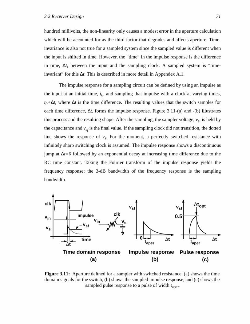
3.2 Receiver Design 71
hundred millivolts, the non-linearity only causes a modest error in the aperture calculation
which will be accounted for as the third factor that degrades and affects aperture. Time-
invariance is also not true for a sampled system since the sampled value is different when
the input is shifted in time. However, the “time” in the impulse response is the difference
in time, ∆t, between the input and the sampling clock. A sampled system is “time-
invariant” for this∆t. This is described in more detail in Appendex A.1.
The impulse response for a sampling circuit can be defined by using an impulse as
the input at an initial time,t0, and sampling that impulse with a clock at varying times,
t0+∆t, where∆t is the time difference. The resulting values that the switch samples for
each time difference,∆t, forms the impulse response. Figure 3.11-(a) and -(b) illustrates
this process and the resulting shape. After the sampling, the sampler voltage,vs, is held by
the capacitance andvsf is the final value. If the sampling clock did not transition, the dotted
line shows the response ofvs. For the moment, a perfectly switched resistance with
infinitely sharp switching clock is assumed. The impulse response shows a discontinuous
jump at∆t=0 followed by an exponential decay at increasing time difference due to the
RC time constant. Taking the Fourier transform of the impulse response yields the
frequency response; the 3-dB bandwidth of the frequency response is the sampling
bandwidth.
Figure 3.11: Aperture defined for a sampler with switched resistance. (a) shows the timedomain signals for the switch, (b) shows the sampled impulse response, and (c) shows the
sampled pulse response to a pulse of width taper.
∆ttime
clk
vin
vs
vin vsvsf
∆t
vsf
0taper
clk
Impulse response
impulse
(a) (b)Time domain response
∆t
vsf
0.5
Pulse response(c)
taper
∆topt
72 Chapter 3: Parallelized I/O Circuits
The sampling aperture is defined as the minimum width of a pulse that can be
sampled and resolved by the comparator to the correct bit. Since the sampled value varies
with ∆t, the definition assumes that the data is sampled at the optimum sampling moment,
∆topt. For binary signalling, the minimum pulse width at the optimum sample point has a
sampled voltage of 1/2 the switching threshold. The minimum pulse width corresponds to
theminimum window in which the integrated value under the impulse response curve is 1/
2. In Figure 3.11-(b), the box with the width marked bytaper is the minimum aperture time
for the corresponding impulse response. Note that the aperture in this simplistic scenario
is roughly 0.7 times the product of the switch ON-resistance and the sampling
capacitance.
Using this aperture definition oftaper for the minimum bit-time does not allow any
margin for errors. For example, an input-offset voltage in the comparator which follows
the sampler would shift the decision threshold to be higher or lower than mid-swing. In
order for the correct bit to be resolved, the integrated value of the normalized impulse
response within the window needs to be greater than 1/2. Therefore, thetaper definition
indicates the absolute maximum sampling rate, and serves as a characteristic of the
response of the sampling network. The effect of errors in sampling and comparing is
considered later with the discussion of aperture uncertainty. As an aside, Johansson in [44]
uses a more conservative estimate of aperture as the minimum bit-time which can account
for the comparator offset. Instead of finding the window of the impulse response where the
integrated value is 50% of the response, he arbitrarily finds the window where the
integrated value is 80%.
Effect of non-ideal switching
The aperture is determined not only by the RC but also by the non-ideal switching
which depends on both the sampling clock switching waveform and the voltage dependent
resistance of the NMOS switch. Because an NMOS device operating in its linear region
has a resistance proportional toVGS-VT, the resistance is non-linear. Figure 3.12-(a) shows
the varying resistance with differentVGS, for a device width of 24λ (6-µm in a 0.5-µm
process technology). Hence, the switch resistance changes with the clock waveform.
Figure 3.12-(b) shows a portion of the sampling clock waveform that drives a FO-4 load.
Superimposed is the time-varying resistance,R(t), of the switch with width of 24λ when
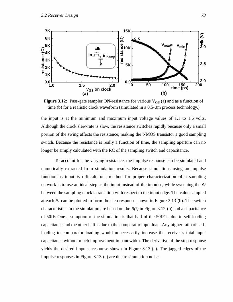
3.2 Receiver Design 73
the input is at the minimum and maximum input voltage values of 1.1 to 1.6 volts.
Although the clock slew-rate is slow, the resistance switches rapidly because only a small
portion of the swing affects the resistance, making the NMOS transistor a good sampling
switch. Because the resistance is really a function of time, the sampling aperture can no
longer be simply calculated with the RC of the sampling switch and capacitance.
To account for the varying resistance, the impulse response can be simulated and
numerically extracted from simulation results. Because simulations using an impulse
function as input is difficult, one method for proper characterization of a sampling
network is to use an ideal step as the input instead of the impulse, while sweeping the∆t
between the sampling clock’s transition with respect to the input edge. The value sampled
at each∆t can be plotted to form the step response shown in Figure 3.13-(b). The switch
characteristics in the simulation are based on theR(t) in Figure 3.12-(b) and a capacitance
of 50fF. One assumption of the simulation is that half of the 50fF is due to self-loading
capacitance and the other half is due to the comparator input load. Any higher ratio of self-
loading to comparator loading would unnecessarily increase the receiver’s total input
capacitance without much improvement in bandwidth. The derivative of the step response
yields the desired impulse response shown in Figure 3.13-(a). The jagged edges of the
impulse responses in Figure 3.13-(a) are due to simulation noise.
Figure 3.12: Pass-gate sampler ON-resistance for various VGS (a) and as a function oftime (b) for a realistic clock waveform (simulated in a 0.5-µm process technology.)
0 50 100 150 2000.0
5K
10K
15K
VminVmax
2.0
2.5
3.0
1.0 1.5 2.00.0
1K
2K
3K
4K
5K
6K
7K
resi
stan
ce (
Ω)
res
ista
nce
(Ω)
clk
(V)
clk
time (ps)(b)(a)
VGS on clock
clk
in insamp
74 Chapter 3: Parallelized I/O Circuits
The three curves in Figure 3.13-(b) illustrate variations on the simulation
parameters. Two different slew rates for the signal switching the sampling gate (based on
the fan-out of the signal) are illustrated (by the triangle and the square curves). The
corresponding aperture sizes,taper, are shown in the legend of Figure 3.13-(a). These two
curves show that the aperture depends considerably on the slew rate of the sampling
signal. Because the ON-resistance of the switch is roughly 600Ω, the aperture for an
ideally switched RC is 1/10 FO-4 (20ps). The finite clock slew rate of a fan-out of two
sampling clock enlarges the sampling aperture by 2 to 3x.
Effect of non-linearity
Also illustrated in the figures are different input transitions for the case of fan-out
of two. Both input rising (square curve) and falling (diamond) steps were simulated with
step size of 500mV. This variation for the different transitions is primarily due to the non-
linearity of the switch. To simulate without the non-linearity of the switch, Figure 3.13-(a)
also shows a star curve that illustrates the results for a small input step size of 10mV with
the same common-mode (1.35V) as the larger swing inputs. The curve is independent of
the type of transition demonstrating that the system is linear with small input voltages. For
the larger signal amplitude responses, an input falling step has lower switch resistance
than a rising step because theVGS increases instead of decreases. The effect can be seen by
the smaller aperture for the falling step, the diamond curve in Figure 3.13-(a) and (b).
Conversely, the rising transition’s response, illustrated by the square curve, has a larger
aperture. The linearity assumption is acceptable primarily because the non-linearity of the
resistance can be bounded by restricting the input swing such that the sampling resistance
variation is small compared to the ON-resistance of the switch.1For input swings as large
as 500mV, the resistance variation is significant enough to cause a rising transition’s
aperture that is 50% larger than the falling transition’s aperture. Any larger voltage swing
would make the linear assumption unsuitable.
Based on the sampling-aperture definition, the minimum sample spacing that
yields distinct sampled values is roughly 1/4 FO-4. However, the minimum bit-time needs
1. The situation is worse for signals with larger dynamic range with multiplex decision levels inapplications such as a multi-level signalling scheme or an analog-to-digital converter.
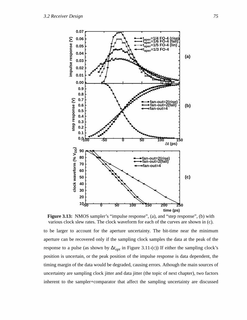
3.2 Receiver Design 75
to be larger to account for the aperture uncertainty. The bit-time near the minimum
aperture can be recovered only if the sampling clock samples the data at the peak of the
response to a pulse (as shown by∆topt in Figure 3.11-(c)) If either the sampling clock’s
position is uncertain, or the peak position of the impulse response is data dependent, the
timing margin of the data would be degraded, causing errors. Athough the main sources of
uncertainty are sampling clock jitter and data jitter (the topic of next chapter), two factors
inherent to the sampler+comparator that affect the sampling uncertainty are discussed
Figure 3.13: NMOS sampler’s “impulse response”, (a), and “step response”, (b) withvarious clock slew rates. The clock waveform for each of the curves are shown in (c).
step
res
pons
e (V
)im
puls
e re
spon
se (
V)
0.00
0.01
0.02
0.03
0.04
0.05
0.06
0.07
taper=1/4 FO-4 (rise)taper=1/6 FO-4 (fall)
taper=1/3 FO-4
-100 -50 0 50 100 1500.00.10.20.30.40.50.60.70.80.9
fan-out=2(rise)fan-out=2(fall)fan-out=4
-50 0 50 100 150 200 25010
20
30
40
50
60
70
80
90
fan-out=2(rise)fan-out=2(fall)fan-out=4
cloc
k w
avef
orm
(%
VD
D)
∆t (ps)
time (ps)
(a)
(b)
(c)
taper=1/5 FO-4 (lin)
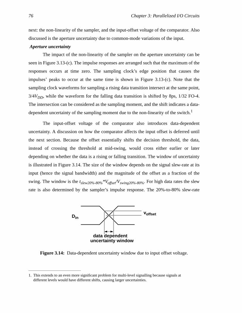
76 Chapter 3: Parallelized I/O Circuits
next: the non-linearity of the sampler, and the input-offset voltage of the comparator. Also
discussed is the aperture uncertainty due to common-mode variations of the input.
Aperture uncertainty
The impact of the non-linearity of the sampler on the aperture uncertainty can be
seen in Figure 3.13-(c). The impulse responses are arranged such that the maximum of the
responses occurs at time zero. The sampling clock’s edge position that causes the
impulses’ peaks to occur at the same time is shown in Figure 3.13-(c). Note that the
sampling clock waveforms for sampling a rising data transition intersect at the same point,
3/4VDD, while the waveform for the falling data transition is shifted by 8ps, 1/32 FO-4.
The intersection can be considered as the sampling moment, and the shift indicates a data-
dependent uncertainty of the sampling moment due to the non-linearity of the switch.1
The input-offset voltage of the comparator also introduces data-dependent
uncertainty. A discussion on how the comparator affects the input offset is deferred until
the next section. Because the offset essentially shifts the decision threshold, the data,
instead of crossing the threshold at mid-swing, would cross either earlier or later
depending on whether the data is a rising or falling transition. The window of uncertainty
is illustrated in Figure 3.14. The size of the window depends on the signal slew-rate at its
input (hence the signal bandwidth) and the magnitude of the offset as a fraction of the
swing. The window is thetslew20%-80%*Voffset/Vswing20%-80%. For high data rates the slew
rate is also determined by the sampler’s impulse response. The 20%-to-80% slew-rate
1. This extends to an even more significant problem for multi-level signalling because signals atdifferent levels would have different shifts, causing larger uncertainties.
Figure 3.14: Data-dependent uncertainty window due to input offset voltage.
voffset
uncertainty window
Din
data dependent
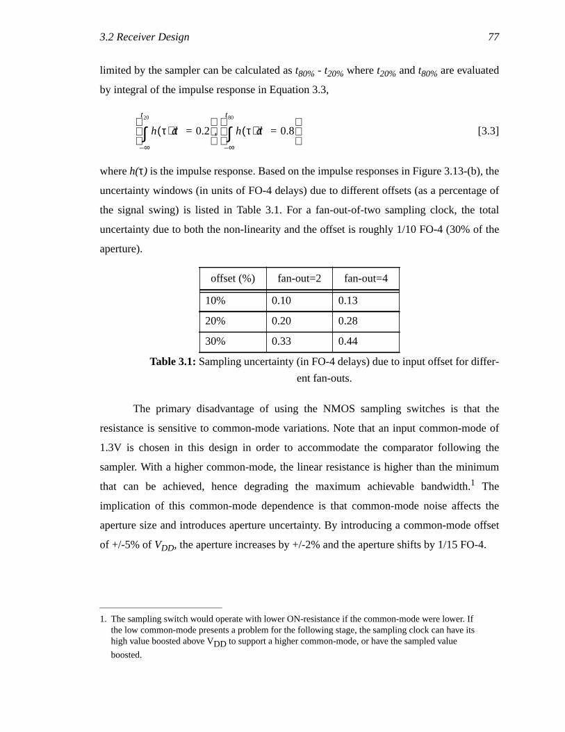
3.2 Receiver Design 77
limited by the sampler can be calculated ast80% - t20% wheret20% andt80% are evaluated
by integral of the impulse response in Equation 3.3,
[3.3]
whereh(τ) is the impulse response. Based on the impulse responses in Figure 3.13-(b), the
uncertainty windows (in units of FO-4 delays) due to different offsets (as a percentage of
the signal swing) is listed in Table 3.1. For a fan-out-of-two sampling clock, the total
uncertainty due to both the non-linearity and the offset is roughly 1/10 FO-4 (30% of the
aperture).
The primary disadvantage of using the NMOS sampling switches is that the
resistance is sensitive to common-mode variations. Note that an input common-mode of
1.3V is chosen in this design in order to accommodate the comparator following the
sampler. With a higher common-mode, the linear resistance is higher than the minimum
that can be achieved, hence degrading the maximum achievable bandwidth.1 The
implication of this common-mode dependence is that common-mode noise affects the
aperture size and introduces aperture uncertainty. By introducing a common-mode offset
of +/-5% ofVDD, the aperture increases by +/-2% and the aperture shifts by 1/15 FO-4.
1. The sampling switch would operate with lower ON-resistance if the common-mode were lower. Ifthe low common-mode presents a problem for the following stage, the sampling clock can have itshigh value boosted above VDD to support a higher common-mode, or have the sampled value
boosted.
offset (%) fan-out=2 fan-out=4
10% 0.10 0.13
20% 0.20 0.28
30% 0.33 0.44
Table 3.1:Sampling uncertainty (in FO-4 delays) due to input offset for differ-
ent fan-outs.
h τ( ) τd
∞–
t20
∫ 0.2=
h τ( ) τd
∞–
t80
∫ 0.8=
,
78 Chapter 3: Parallelized I/O Circuits
Sampler summary
To summarize, the minimum sample spacing can be calculated by combining the
aperture window and the uncertainty (without clock jitter). The result is roughly 1/3 FO-4
based on the following assumptions: the input-offset voltage is 10% ofVswing, the clock
slew-rate is fan-out of two, total sampling capacitance is 2x self-loading, and the common-
mode noise is less than 10% ofVDD. The minimum bit-time based on Johansson’s more
conservative definition is roughly 1/2 FO-4. The bit-time does not change significantly
with modest changes in the implementation-dependent values used in the calculation. The
most significant improvement can be made by reducing the load capacitance of the
sampling switch to be less than the switch’s self-loading. Realistically, reducing the effect
of loading capacitance requires much larger sampling devices, which would present
excessive input capacitance. The impact of the input-offset voltage of the comparator can
be reduced by either designing one with lower offsets or increasing the voltage swing.
Based on simulation, reducing voltage offsets to 5% of the swing only reduces the
aperture by at most 15%. Lastly, sharpening the clock slew-rate from fan-out of 2 to fan-
out of 1 only improves the aperture by 10%.
In the above analysis, the minimum bit-time is only a function of the relative size
of the sampling device and its load capacitance. The absolute device size is very important
because it sets the input capacitance and hence the input bandwidth. The sampler input
capacitance is especially important in a demultiplexing architecture where the number of
sampling switches on an input is large. The design of the comparator becomes a balancing
act between the input capacitance and the offset voltage. The following section discusses
the implementation of a comparator and addresses this issue.
3.2.2 Comparator designThe circuit diagram for the input sampler+comparator used in this design is shown in
Figure 3.15. For better noise rejection, the circuit is designed with differential inputs. The
regenerative amplifier following the samplers is a slight variation of the comparator by
Yukawa in [105]. When the clock isHIGH, the NMOS transistors in the middle of the
stack disconnect the upper and lower cross-coupled devices, resetting the latch. During
this phase, the sampler is tracking, and the latch outputs are prechargedHIGH while the
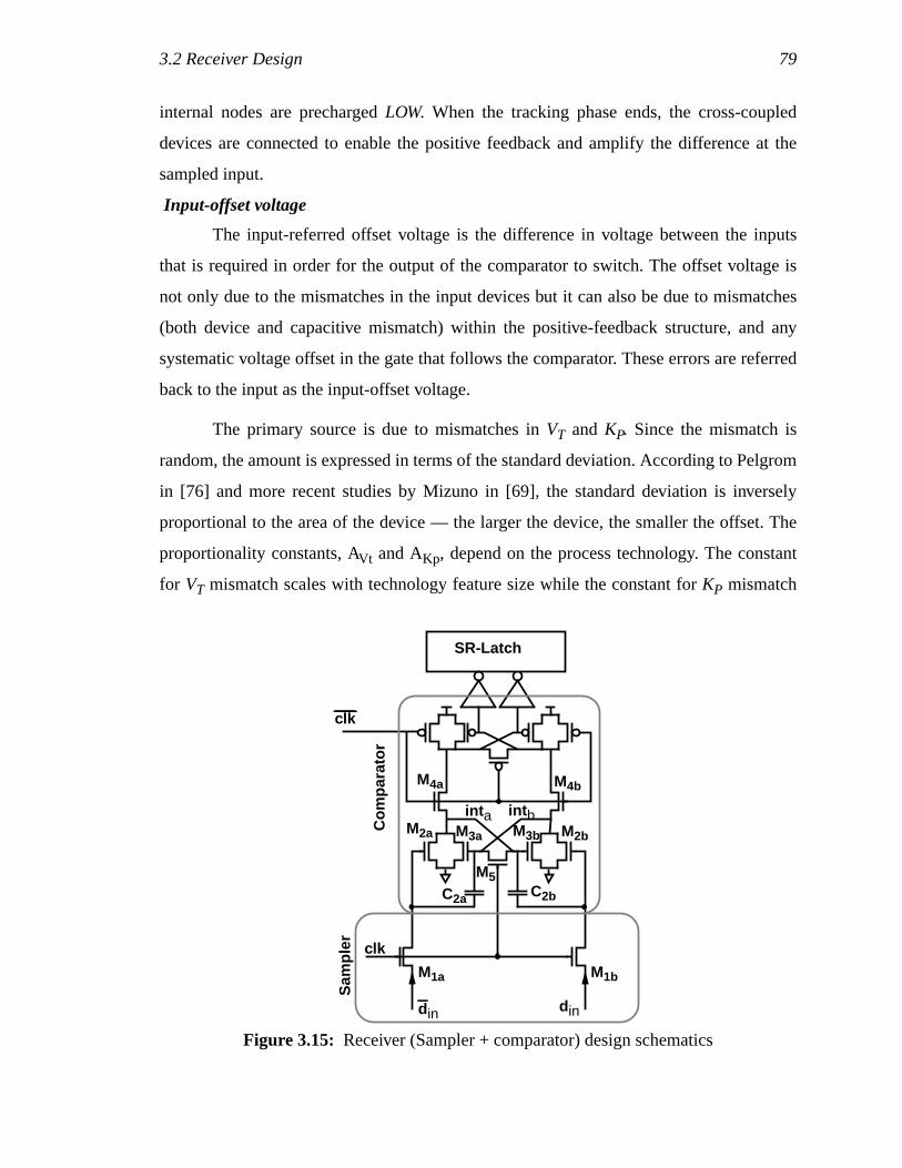
3.2 Receiver Design 79
internal nodes are prechargedLOW. When the tracking phase ends, the cross-coupled
devices are connected to enable the positive feedback and amplify the difference at the
sampled input.
Input-offset voltage
The input-referred offset voltage is the difference in voltage between the inputs
that is required in order for the output of the comparator to switch. The offset voltage is
not only due to the mismatches in the input devices but it can also be due to mismatches
(both device and capacitive mismatch) within the positive-feedback structure, and any
systematic voltage offset in the gate that follows the comparator. These errors are referred
back to the input as the input-offset voltage.
The primary source is due to mismatches inVT andKP. Since the mismatch is
random, the amount is expressed in terms of the standard deviation. According to Pelgrom
in [76] and more recent studies by Mizuno in [69], the standard deviation is inversely
proportional to the area of the device — the larger the device, the smaller the offset. The
proportionality constants, AVt and AKp, depend on the process technology. The constant
for VT mismatch scales with technology feature size while the constant forKP mismatch
Figure 3.15: Receiver (Sampler + comparator) design schematics
din din
clk
clk
C2a C2b
M1a M1b
SR-Latch
Com
para
tor
Sam
pler
M2a M2bM3a M3b
M4a M4b
M5
int a int b
80 Chapter 3: Parallelized I/O Circuits
scales more slowly. After roughly normalizing the mismatch parameters by process
technology, the AVt is roughly 28mV-λ, and AKp is roughly 1.5%-µm1. Based on the
analysis of the previous section, the aperture does not degrade significantly with an input
offset voltage of the latch at +/-10% of the swing. If the minimum signal swing is 300mV,
a +/- 3σ input-offset voltage of less than 60mV is sufficient.
The offsets due to the input transistors,M2a,b, contribute to at least half of the total
input-offset voltage. To keep the peak voltage mismatch to less than 40mV in the 0.5-µm
process technology, a minimum-device width of 10λ is required. TheVT mismatch
between the input transistors directly corresponds to a standard deviation of 6mV. TheKP
mismatch is translated into input-offset voltage by dividing the mismatch in current by the
gm of the device. With a common-mode voltage of 1.3V (to keep the input devices in
saturation)2, the effective input-offset voltage due to theKP mismatch has a standard
deviation of 1.3mV. Note that the effect ofVT mismatch is generally larger thanKP
mismatch, especially at lowVGS.
The regenerative structure of Figure 3.15 also contributes to the total input-referred
offset voltage. For correct operation, when the clock transistors are enabled, the current
difference from the differential transistor pair must be greater than the current difference
due to the offsets from the clocked transistor,M4a,b, and the cross-coupled devices,M3a,b.
The clocked transistor contributes a smaller offset component because theVGS is large,
making the current difference due to itsVT mismatches small in comparison. Also, to
minimize the series resistance for faster regeneration, the clocked devices,M3a,b, are sized
larger than the input devices, thus the offset is less. The cross-coupled devices,M4a,b (and
the corresponding PMOS devices3), are initially in the off-state, and therefore do not
contribute any offset. However when the internal nodes,inta,b, rise aboveVT as the clock
transitions HIGH, the cross-coupled feedback is enabled and their mismatches are
1. The proportionality constants are the standard deviation of the voltage and current mismatch. Thepeak-to-peak values are roughly 6x the standard deviation.
2. Thegm per width for the NMOS transistor is 30µS/λ, and the current for the bias condition is roughly30µΑ/λ
3. The PMOS cross-coupled devices contribute to the input-referred offset with a similar mechanism asthe NMOS cross-coupled devices. They are typically larger devices so the contribution is smaller.
3.2 Receiver Design 81
introduced as offset. This offset can be reduced by slowly charging the internal nodes [62].
When the voltage charges toVT, the offsets do not have any impact, if the voltage
difference of the internal nodes is greater than the voltage offset due to the mismatches of
the cross-coupled devices. The charging rate can be controlled by the clock slew rate and
the size of the clocked transistors. However, the charging cannot be too slow because it
lengthens the cycle-time. A 40-mV offset can be reduced by half with a charging delay of
only 250ps.
In the implementation of the sampler of the transceiver test chip in the 0.5-µm
process technology, the input devices are conservatively sized to be 12λ. The +/- 3σ input-
offset voltage accounting for all the transistors in the comparator structure is less than
60mV.
Maximum number of parallel samplers
Based on the size of the input device of the comparator, the device size of the
sampler can be calculated. In order to keep the sampler loading (or the input capacitance
of the comparator) roughly equal to the self-loading, the sampling switch size is roughly
24λ.
Since the receiver will demultiplex and oversample the data, the input capacitance
due to the parallel samplers must be small enough not to limit the input bandwidth. The
input capacitance of each sampler is then the sum of the sampler’s source capacitance and
half of the sampling capacitance. The sampling capacitance is halved because only half of
the sampling switches are in the sampling phase at any time. Each sampler input
capacitance is roughly 50fF in the 0.5-µm process technology. For a minimum bit-time of
1/2 FO-4 from the sampler analysis in a 25-Ω environment, the maximum number of
samplers can be as large as 45 before the data bandwidth is limited. However, if parasitic
capacitances, such as pad capacitance and the on-chip termination PMOS, are included,
the maximum number of samplers in parallel is reduced to roughly 35.
Number of samplers for demultiplexing
The minimum number of samplers in parallel depends on the degree of
demultiplexing, which is the ratio between the cycle-time and the bit-time. The
regenerative amplifier (comparator) topology is used instead of a linear amplifier so that
82 Chapter 3: Parallelized I/O Circuits
the positive feedback provides high gain (that grows exponentially with the evaluation
time as expressed in Equation 3.4 [83]) with low power and area:
[3.4]
The regenerative time constant,τ=C/gm, determines the growth of the exponential gain.
This gain amplifies the sampled value that is coupled onto the comparator throughM2a,b.
For the Yukawa comparator built in a 0.5-µm process technology, the time constant is
roughly 200ps (less than 1 FO-4). An evaluation time of 4-FO-4 (cycle-time of 8 FO-4) is
sufficient to resolve 10mV to greater than 400mV. BecauseM4a,b is in series with the
cross-coupled transistors, thegm is degenerated, which increases the regeneration time.
Alternative structures, such as an inverter-feedback structure, can potentially have a cycle-
time of nearly 6 FO-4. However, note that since 8 FO-4 is also the clock-period limitation
of the clock buffers and digital logic1, a comparator with cycle-time faster than 8 FO-4 is
not necessary. With a minimum bit-time of 1/2 FO-4, the required amount of
demultiplexing is roughly 16.
For the transceiver implemented in the 0.5-µm process technology, 1 FO-4 is used
as the bit-time targeting a data rate of 4Gb/s. Only 8 sampler+comparators are needed for
the demultiplexing. The implementation used 24 samplers to oversample for the timing
recovery. The total capacitance, including interconnect and termination device, tallies to
roughly 2.0pF which limits the data bandwidth to 5Gb/s (using a bit-time of roughly 2RC
and 50Ω resistance).
3.2.3 Second-order receiver-design issuesBeside the primary issues of the sensitivity of the comparator and the input bandwidth, a
number of second-order implementation issues affect the performance of the receiver. This
section discusses the following considerations: setting the input common-mode voltage,
clock timing, minimizing the charge kickback, and reducing metastability.
1. Alternative sampler+comparator style using the regeneration as part of the sampling, as done byDEC and Fiedler [28], requires a fast time constant not only for short cycle-time but also for a smallsampling aperture.
Gain et τ⁄
=
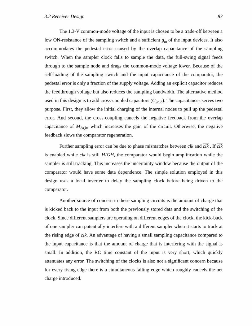
3.2 Receiver Design 83
The 1.3-V common-mode voltage of the input is chosen to be a trade-off between a
low ON-resistance of the sampling switch and a sufficientgm of the input devices. It also
accommodates the pedestal error caused by the overlap capacitance of the sampling
switch. When the sampler clock falls to sample the data, the full-swing signal feeds
through to the sample node and drags the common-mode voltage lower. Because of the
self-loading of the sampling switch and the input capacitance of the comparator, the
pedestal error is only a fraction of the supply voltage. Adding an explicit capacitor reduces
the feedthrough voltage but also reduces the sampling bandwidth. The alternative method
used in this design is to add cross-coupled capacitors (C2a,b). The capacitances serves two
purpose. First, they allow the initial charging of the internal nodes to pull up the pedestal
error. And second, the cross-coupling cancels the negative feedback from the overlap
capacitance ofM2a,b, which increases the gain of the circuit. Otherwise, the negative
feedback slows the comparator regeneration.
Further sampling error can be due to phase mismatches betweenclk andclk . If clk
is enabled whileclk is still HIGH, the comparator would begin amplification while the
sampler is still tracking. This increases the uncertainty window because the output of the
comparator would have some data dependence. The simple solution employed in this
design uses a local inverter to delay the sampling clock before being driven to the
comparator.
Another source of concern in these sampling circuits is the amount of charge that
is kicked back to the input from both the previously stored data and the switching of the
clock. Since different samplers are operating on different edges of the clock, the kick-back
of one sampler can potentially interfere with a different sampler when it starts to track at
the rising edge ofclk. An advantage of having a small sampling capacitance compared to
the input capacitance is that the amount of charge that is interfering with the signal is
small. In addition, the RC time constant of the input is very short, which quickly
attenuates any error. The switching of the clocks is also not a significant concern because
for every rising edge there is a simultaneous falling edge which roughly cancels the net
charge introduced.
84 Chapter 3: Parallelized I/O Circuits
Although the bandwidth of the comparator is not critical, a fast comparator with
high gm/C has the advantage of reducing the metastability probability, which allows fewer
pipeline stages. The mean time between failure, an indication of the metastability
probability, can be calculated using
from Portmann in [77] [3.5]
whereτ is the regenerative time constant,tr is the regeneration time, andTo is a topology-
and-process-dependent constant. A trade-off is made in the comparator used in this
design. The amount of time for regeneration is reduced because the internal nodes are
charged up slowly for a better input-offset voltage. Furthermore, the time constant is also
longer because the clock switch that is used to break the positive feedback reduces the
effective gm. The metastability mean-time-between-failure (MTBF) of the comparator
structure is simulated/calculated to be 1.6µs with each parameter extrapolated from
simulation (τ is 130ps, roughly 0.5 FO-4, andTo is 5x10⁻⁹sec). Because the MTBF is not
sufficiently long to guarantee a low BER, further synchronization pipelining was
implemented in the following stages.
3.2.4 SR-latch designIn order to remove the precharge phase from the output and to present a constant (non-
data-dependent) load to the comparator, the comparator is followed by an SR-latch.
Presenting a constant load is especially important because writing a new value into the
latch requires the new value to overdrive the stored value. Inherently, there is hysteresis
which translates effectively into an input-offset voltage that is data dependent. The amount
of the input-offset voltage depends on the voltage required to store a new value, and also
the gain of the comparator. The effect of this error is shown in Figure 3.16-(a). Unlike the
offset voltage described previously in Figure 3.12, this offset is different for the two
different transitions. If the two offsets are the same (but of different sign), the result would
be a simple shift in the time position where the data is sampled, a static phase offset,toffset.
Because the timing-recovery circuit can roughly track offsets, this is not a serious
problem. However, if the offsets are not the same for the different transitions, an
MTBF 1 f data f clk To etr τ⁄–
⋅ ⋅ ⋅( )⁄=
3.2 Receiver Design 85
uncertainty window results. A latch used in this design that reduces this error is discussed
below and shown in Figure 3.16-(b).
Because the output voltages are prechargedHIGH, the data is inverted prior to
driving it to a NOR structure. The inverters serve a dual purpose of appearing as a fixed
(non-data-dependent loading) and providing additional amplification. The inverter P:N
ratio is carefully chosen so that its switching point matches that of the comparator to
minimize the systematic offset. The feedback devices in the cross-coupled NORs are
made as weak as possible to reduce the amount of voltage required to overdrive the stored
value. Because a NOR feedback structure is slow due to the series PMOS, a minor
modification can be made to increase the speed. A bypass path can be used to pull up the
output with a PMOS directly instead of using the NOR structure. Since the inputs to the
NOR structure are both low during the comparator’s precharge phase, the outputs are not
disturbed by the bypass path. When one of the input assertsHIGH, one output is pulled
down by the NOR while the other is pulled up with the PMOS.
3.2.5 ScalabilityThe final issue with the receiver design is whether the data bandwidth scales with
technology. In order for the scaling to occur, the factors that influence the sampling
aperture must scale. Furthermore, depending on whether the signal amplitude scales, the
input resolution may need to scale.
Figure 3.16: SR-latch structures that minimize data-dependent loading.
(a) (b)DoutDout DoutDout
DinDin
serial voffsetHL voffsetLH
toffset
data
86 Chapter 3: Parallelized I/O Circuits
The sampling clock transition time scales with the FO-4 metric. All capacitances
scale while the scaling of the sampling device would maintain the same resistance, so the
RC time constants potentially scale with feature sizes. So to the first order, the aperture
can be expected to scale. However, ifVT does not scale linearly with supply voltage (as is
often the case with non-ideal scaling), the NMOS sampling device’s linear resistance
would increase, especially since the common-mode voltage of the comparator would need
to be higher to keep the input devices conducting. This poses a problem with the chosen
topology. An alternative topology that integrates the sampling with the comparator [99]
may scale better as supply voltage is lowered.
Although the RC time constants roughly scales with technology,VT mismatches
between devices stay constant andKP mismatches become worse. So as devices scale, the
aperture uncertainty and input resolution become much more significant, requiring offset-
cancellation schemes [83]. Typically, active offset-cancellation techniques have penalized
the data rates because of the additional offset-cancellation phase that the comparator needs
to detect the offset voltage, and because of the settling time needed for the feedback to
cancel the offset accurately. Techniques that would apply to high-speed links are an
interesting area of future research.
3.2.6 Receiver summaryThis section discussed the design of a receiver that operates near the limits of the
technology using a sampler+comparator architecture. To reach very high data rates, an
NMOS sampling switch is used to sample the data. To maintain good resolution, common-
mode noise is reduced using a symmetric, differential structure. The input resolution of
the receiver is primarily limited by the input-referred offset voltage of the comparator
following the sampler, which in turn depends on the device mismatches. Because the
offset voltage also affects the aperture uncertainty, the minimum bit-time increases with
larger offsets or alternatively with smaller input swing. Based on the characterization of
the sampling switch and the comparator, the receiver can achieve bit-times of less than 1/2
FO-4 and resolution of 60mV with small enough input capacitance per sampler to allow
more than 30 samplers in parallel without limiting the bandwidth.
3.3 Summary 87
3.3 SummaryThis chapter shows how one can use the low off-chip impedance to implement a higher
degree of parallelism. Signalling at a higher number of bits/clock cycle improves the
minimum bit-time of both the transmitter and the receiver. The transmitter can operate
with bit-times of less than 3/4 FO-4 and the receiver can operate at less than 1/2 FO-4. The
limitations of the transmitter are the transition time of the on-chip signal, and the inherent
filtering due to the output capacitance. The limitations of the receiver are how quickly the
data can be sampled and the inherent filtering of the input capacitance. The maximum
sampling rate is determined by the sampling aperture (which depends primarily on the
switch RC and the slew-rate of the clock) and the aperture uncertainty (which depends
primarily on the input-offset voltage of the comparator).
The analysis has so far assumed zero clock jitter even though jitter is one of the
most significant sources of aperture uncertainty. We further assumed ideal phase spacing
between clocks. The next chapter begins with a discussion on methods to generate the
precise clock phases needed for multiplexing and demultiplexing, and factors that limit the
precision of these clocks.

88 Chapter 3: Parallelized I/O Circuits
89
Chapter 4
Clock Generation and Timing Recovery
The previous chapter assumed that the clock for the transmitter and receiver were from an
ideal source. This chapter addresses the issues in generating the clocks for a very high
data-rate system. Since most high-speed links use a phase-locked loop (PLL) to generate
the clock, the next section explores phase-locked loop design in more detail, paying
particular attention to the sources of phase noise in the system. Section 4.2 then discusses
how the PLL design can be extended to generate the multiple clock phases that are used by
the multiplexing transmitter and demultiplexing receiver. Since the bit-times are defined
by the spacing between the clock phases, the section describes the primary causes of phase
spacing errors and provides some measured results.
In addition to generating the clock phases, the phases for the receiver must be
aligned with respect to the input data stream to receive the data with maximum timing
margin. To perform the alignment, phase information must be extracted from the input.
Two architectures have been proposed in Section 2.3: a phase-picking scheme that
oversamples the data, and a data-recovery PLL that aligns the PLL output to the phase of
the input data. These two architectures are compared in Section 4.3 in terms of the static
phase error and the jitter that each would introduce. Traditionally, PLLs have been used
for high data rates. Phase-picking architectures with high degree of oversampling have not
been used due to the larger complexity and area and power overhead. Because the results
from the previous chapter on the sampling aperture suggest that the samplers can sample
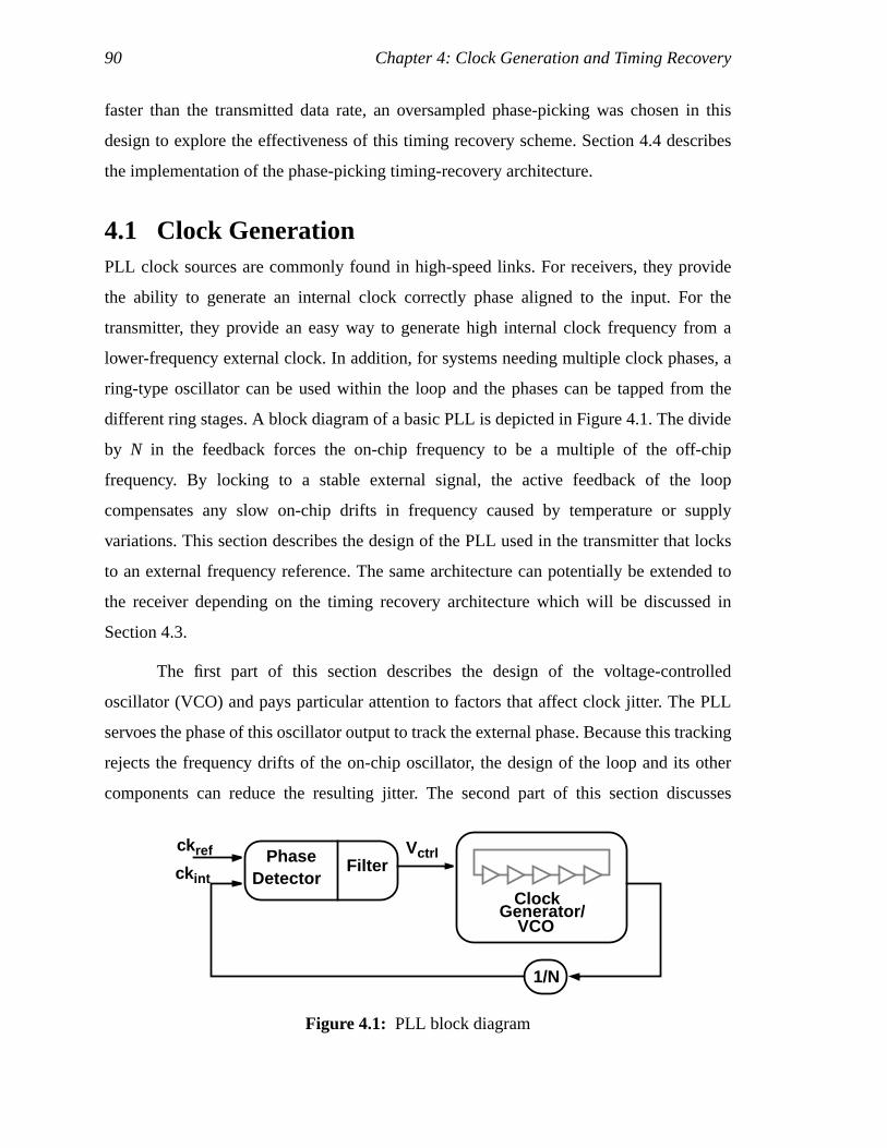
90 Chapter 4: Clock Generation and Timing Recovery
faster than the transmitted data rate, an oversampled phase-picking was chosen in this
design to explore the effectiveness of this timing recovery scheme. Section 4.4 describes
the implementation of the phase-picking timing-recovery architecture.
4.1 Clock GenerationPLL clock sources are commonly found in high-speed links. For receivers, they provide
the ability to generate an internal clock correctly phase aligned to the input. For the
transmitter, they provide an easy way to generate high internal clock frequency from a
lower-frequency external clock. In addition, for systems needing multiple clock phases, a
ring-type oscillator can be used within the loop and the phases can be tapped from the
different ring stages. A block diagram of a basic PLL is depicted in Figure 4.1. The divide
by N in the feedback forces the on-chip frequency to be a multiple of the off-chip
frequency. By locking to a stable external signal, the active feedback of the loop
compensates any slow on-chip drifts in frequency caused by temperature or supply
variations. This section describes the design of the PLL used in the transmitter that locks
to an external frequency reference. The same architecture can potentially be extended to
the receiver depending on the timing recovery architecture which will be discussed in
Section 4.3.
The first part of this section describes the design of the voltage-controlled
oscillator (VCO) and pays particular attention to factors that affect clock jitter. The PLL
servoes the phase of this oscillator output to track the external phase. Because this tracking
rejects the frequency drifts of the on-chip oscillator, the design of the loop and its other
components can reduce the resulting jitter. The second part of this section discusses
Figure 4.1: PLL block diagram
PhaseDetector
ClockGenerator/
Filterck int
ck ref
VCO
Vctrl
1/N
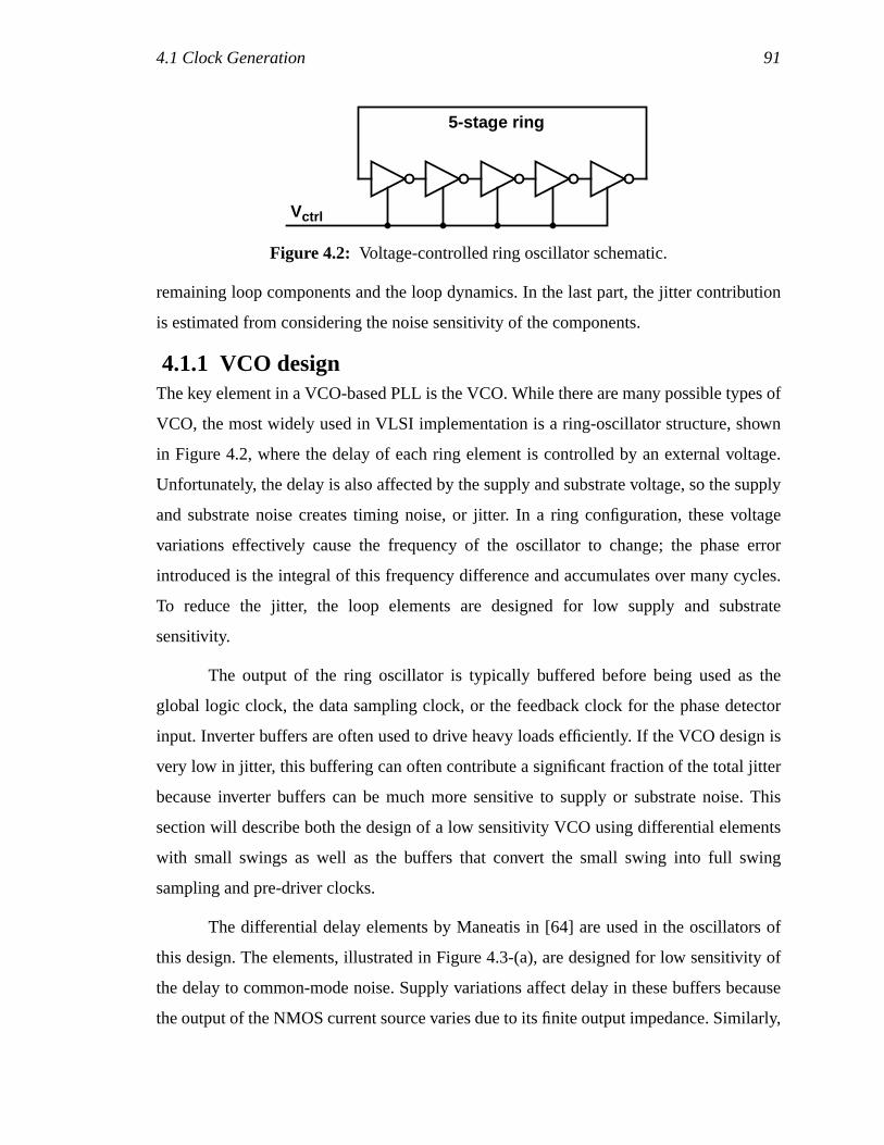
4.1 Clock Generation 91
remaining loop components and the loop dynamics. In the last part, the jitter contribution
is estimated from considering the noise sensitivity of the components.
4.1.1 VCO designThe key element in a VCO-based PLL is the VCO. While there are many possible types of
VCO, the most widely used in VLSI implementation is a ring-oscillator structure, shown
in Figure 4.2, where the delay of each ring element is controlled by an external voltage.
Unfortunately, the delay is also affected by the supply and substrate voltage, so the supply
and substrate noise creates timing noise, or jitter. In a ring configuration, these voltage
variations effectively cause the frequency of the oscillator to change; the phase error
introduced is the integral of this frequency difference and accumulates over many cycles.
To reduce the jitter, the loop elements are designed for low supply and substrate
sensitivity.
The output of the ring oscillator is typically buffered before being used as the
global logic clock, the data sampling clock, or the feedback clock for the phase detector
input. Inverter buffers are often used to drive heavy loads efficiently. If the VCO design is
very low in jitter, this buffering can often contribute a significant fraction of the total jitter
because inverter buffers can be much more sensitive to supply or substrate noise. This
section will describe both the design of a low sensitivity VCO using differential elements
with small swings as well as the buffers that convert the small swing into full swing
sampling and pre-driver clocks.
The differential delay elements by Maneatis in [64] are used in the oscillators of
this design. The elements, illustrated in Figure 4.3-(a), are designed for low sensitivity of
the delay to common-mode noise. Supply variations affect delay in these buffers because
the output of the NMOS current source varies due to its finite output impedance. Similarly,
Figure 4.2: Voltage-controlled ring oscillator schematic.
5-stage ring
Vctrl
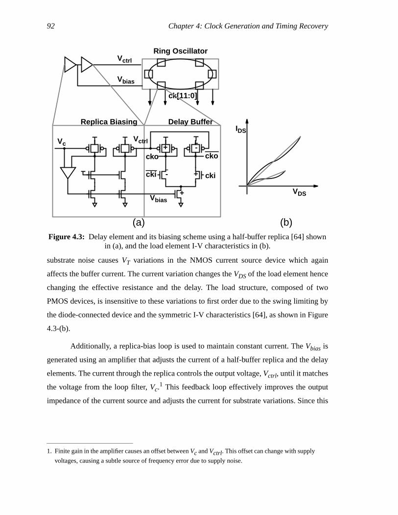
92 Chapter 4: Clock Generation and Timing Recovery
substrate noise causesVT variations in the NMOS current source device which again
affects the buffer current. The current variation changes theVDS of the load element hence
changing the effective resistance and the delay. The load structure, composed of two
PMOS devices, is insensitive to these variations to first order due to the swing limiting by
the diode-connected device and the symmetric I-V characteristics [64], as shown in Figure
4.3-(b).
Additionally, a replica-bias loop is used to maintain constant current. TheVbias is
generated using an amplifier that adjusts the current of a half-buffer replica and the delay
elements. The current through the replica controls the output voltage,Vctrl, until it matches
the voltage from the loop filter,Vc.1 This feedback loop effectively improves the output
impedance of the current source and adjusts the current for substrate variations. Since this
1. Finite gain in the amplifier causes an offset betweenVc andVctrl. This offset can change with supply
voltages, causing a subtle source of frequency error due to supply noise.
Figure 4.3: Delay element and its biasing scheme using a half-buffer replica [64] shownin (a), and the load element I-V characteristics in (b).
Vbias
VctrlVc
cki cki
cko cko
Delay BufferReplica Biasing
Ring OscillatorVctrl
Vbias
ck[11:0]
+
+
-
-
+
(a) (b)
VDS
IDS
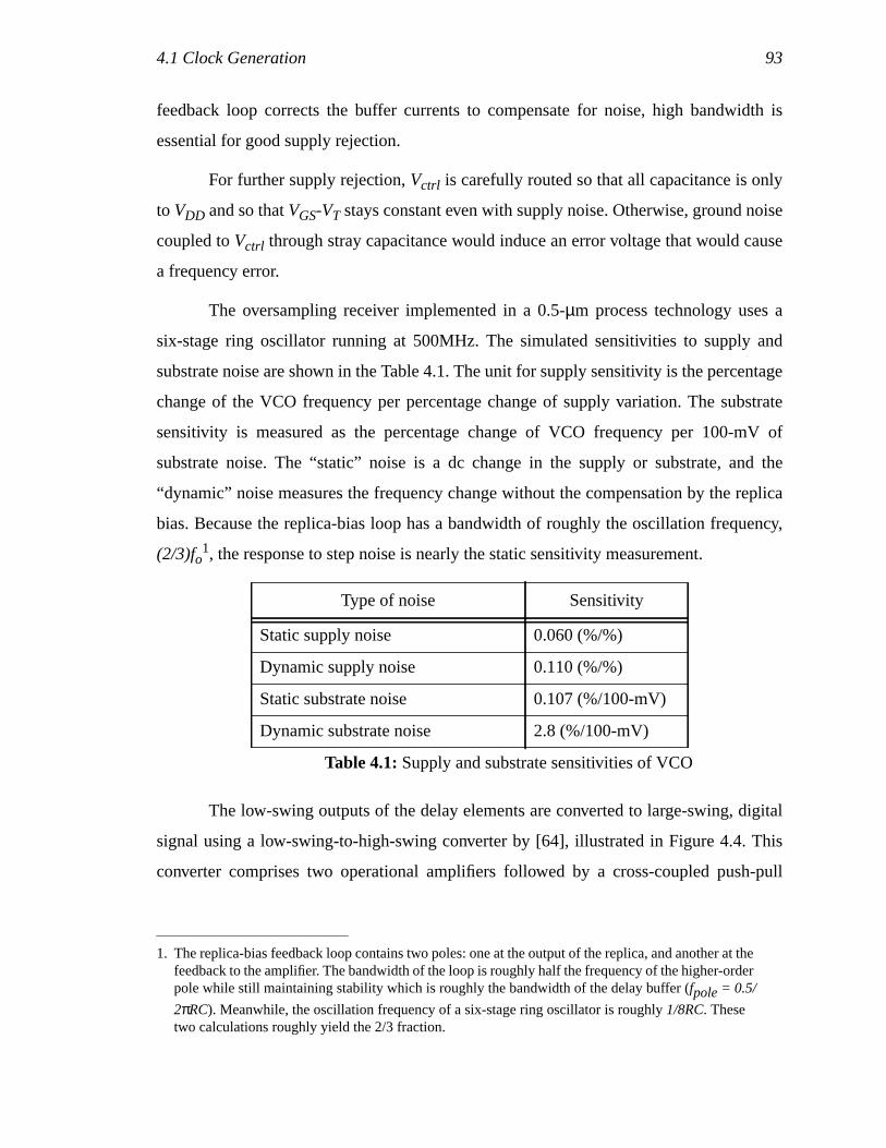
4.1 Clock Generation 93
feedback loop corrects the buffer currents to compensate for noise, high bandwidth is
essential for good supply rejection.
For further supply rejection,Vctrl is carefully routed so that all capacitance is only
to VDD and so thatVGS-VT stays constant even with supply noise. Otherwise, ground noise
coupled toVctrl through stray capacitance would induce an error voltage that would cause
a frequency error.
The oversampling receiver implemented in a 0.5-µm process technology uses a
six-stage ring oscillator running at 500MHz. The simulated sensitivities to supply and
substrate noise are shown in the Table 4.1. The unit for supply sensitivity is the percentage
change of the VCO frequency per percentage change of supply variation. The substrate
sensitivity is measured as the percentage change of VCO frequency per 100-mV of
substrate noise. The “static” noise is a dc change in the supply or substrate, and the
“dynamic” noise measures the frequency change without the compensation by the replica
bias. Because the replica-bias loop has a bandwidth of roughly the oscillation frequency,
(2/3)fo1, the response to step noise is nearly the static sensitivity measurement.
The low-swing outputs of the delay elements are converted to large-swing, digital
signal using a low-swing-to-high-swing converter by [64], illustrated in Figure 4.4. This
converter comprises two operational amplifiers followed by a cross-coupled push-pull
1. The replica-bias feedback loop contains two poles: one at the output of the replica, and another at thefeedback to the amplifier. The bandwidth of the loop is roughly half the frequency of the higher-orderpole while still maintaining stability which is roughly the bandwidth of the delay buffer (fpole = 0.5/
2πRC). Meanwhile, the oscillation frequency of a six-stage ring oscillator is roughly1/8RC. Thesetwo calculations roughly yield the 2/3 fraction.
Type of noise Sensitivity
Static supply noise 0.060 (%/%)
Dynamic supply noise 0.110 (%/%)
Static substrate noise 0.107 (%/100-mV)
Dynamic substrate noise 2.8 (%/100-mV)
Table 4.1:Supply and substrate sensitivities of VCO
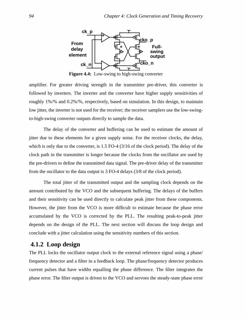
94 Chapter 4: Clock Generation and Timing Recovery
amplifier. For greater driving strength in the transmitter pre-driver, this converter is
followed by inverters. The inverter and the converter have higher supply sensitivities of
roughly 1%/% and 0.2%/%, respectively, based on simulation. In this design, to maintain
low jitter, the inverter is not used for the receiver; the receiver samplers use the low-swing-
to-high-swing converter outputs directly to sample the data.
The delay of the converter and buffering can be used to estimate the amount of
jitter due to these elements for a given supply noise. For the receiver clocks, the delay,
which is only due to the converter, is 1.5 FO-4 (3/16 of the clock period). The delay of the
clock path in the transmitter is longer because the clocks from the oscillator are used by
the pre-drivers to define the transmitted data signal. The pre-driver delay of the transmitter
from the oscillator to the data output is 3 FO-4 delays (3/8 of the clock period).
The total jitter of the transmitted output and the sampling clock depends on the
amount contributed by the VCO and the subsequent buffering. The delays of the buffers
and their sensitivity can be used directly to calculate peak jitter from these components.
However, the jitter from the VCO is more difficult to estimate because the phase error
accumulated by the VCO is corrected by the PLL. The resulting peak-to-peak jitter
depends on the design of the PLL. The next section will discuss the loop design and
conclude with a jitter calculation using the sensitivity numbers of this section.
4.1.2 Loop designThe PLL locks the oscillator output clock to the external reference signal using a phase/
frequency detector and a filter in a feedback loop. The phase/frequency detector produces
current pulses that have widths equalling the phase difference. The filter integrates the
phase error. The filter output is driven to the VCO and servoes the steady-state phase error
Figure 4.4: Low-swing to high-swing converter
ck_p
ck_n
cko_p
cko_n
+ - -
+ +Fromdelay
element
Full-swingoutput
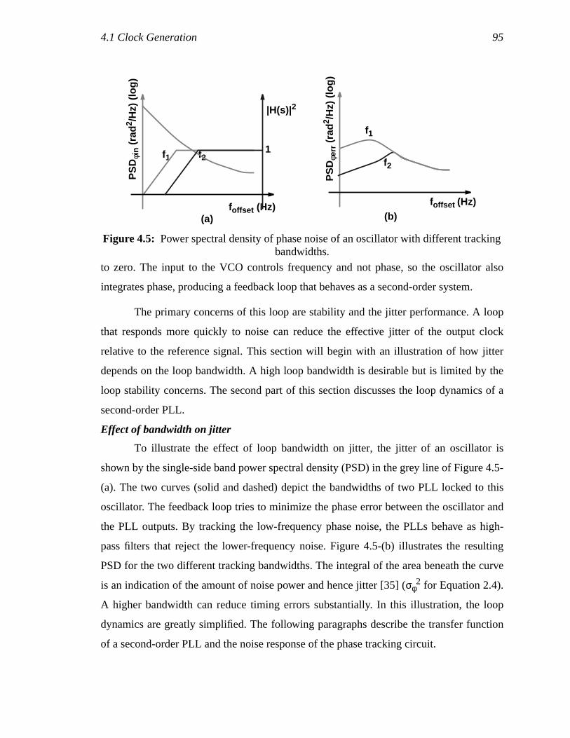
4.1 Clock Generation 95
to zero. The input to the VCO controls frequency and not phase, so the oscillator also
integrates phase, producing a feedback loop that behaves as a second-order system.
The primary concerns of this loop are stability and the jitter performance. A loop
that responds more quickly to noise can reduce the effective jitter of the output clock
relative to the reference signal. This section will begin with an illustration of how jitter
depends on the loop bandwidth. A high loop bandwidth is desirable but is limited by the
loop stability concerns. The second part of this section discusses the loop dynamics of a
second-order PLL.
Effect of bandwidth on jitter
To illustrate the effect of loop bandwidth on jitter, the jitter of an oscillator is
shown by the single-side band power spectral density (PSD) in the grey line of Figure 4.5-
(a). The two curves (solid and dashed) depict the bandwidths of two PLL locked to this
oscillator. The feedback loop tries to minimize the phase error between the oscillator and
the PLL outputs. By tracking the low-frequency phase noise, the PLLs behave as high-
pass filters that reject the lower-frequency noise. Figure 4.5-(b) illustrates the resulting
PSD for the two different tracking bandwidths. The integral of the area beneath the curve
is an indication of the amount of noise power and hence jitter [35] (σφ2 for Equation 2.4).
A higher bandwidth can reduce timing errors substantially. In this illustration, the loop
dynamics are greatly simplified. The following paragraphs describe the transfer function
of a second-order PLL and the noise response of the phase tracking circuit.
Figure 4.5: Power spectral density of phase noise of an oscillator with different trackingbandwidths.
foffset (Hz)
PS
Dφi
n (
rad
2 /H
z) (
log)
f1 f2
|H(s)|2
1
PS
Dφe
rr (
rad
2 /H
z) (
log)
f1
f2
foffset (Hz)
(a) (b)
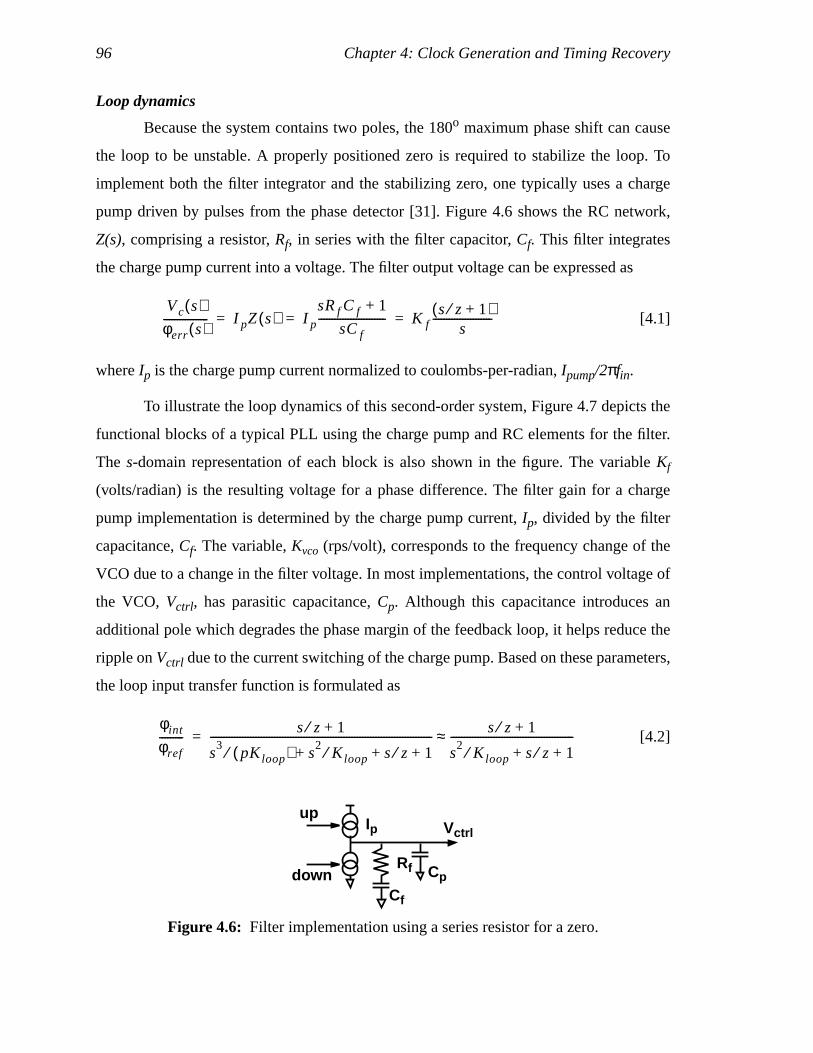
96 Chapter 4: Clock Generation and Timing Recovery
Loop dynamics
Because the system contains two poles, the 180o maximum phase shift can cause
the loop to be unstable. A properly positioned zero is required to stabilize the loop. To
implement both the filter integrator and the stabilizing zero, one typically uses a charge
pump driven by pulses from the phase detector [31]. Figure 4.6 shows the RC network,
Z(s), comprising a resistor,Rf, in series with the filter capacitor,Cf. This filter integrates
the charge pump current into a voltage. The filter output voltage can be expressed as
[4.1]
whereIp is the charge pump current normalized to coulombs-per-radian,Ipump/2πfin.
To illustrate the loop dynamics of this second-order system, Figure 4.7 depicts the
functional blocks of a typical PLL using the charge pump and RC elements for the filter.
The s-domain representation of each block is also shown in the figure. The variableKf
(volts/radian) is the resulting voltage for a phase difference. The filter gain for a charge
pump implementation is determined by the charge pump current,Ip, divided by the filter
capacitance,Cf. The variable,Kvco (rps/volt), corresponds to the frequency change of the
VCO due to a change in the filter voltage. In most implementations, the control voltage of
the VCO,Vctrl, has parasitic capacitance,Cp. Although this capacitance introduces an
additional pole which degrades the phase margin of the feedback loop, it helps reduce the
ripple onVctrl due to the current switching of the charge pump. Based on these parameters,
the loop input transfer function is formulated as
[4.2]
Vc s( )φerr s( )----------------- I pZ s( ) I p
sRf C f 1+
sCf------------------------- K f
s z⁄ 1+( )s
----------------------= = =
Figure 4.6: Filter implementation using a series resistor for a zero.
Rf
Cf
Ip
Cp
Vctrl
up
down
φint
φref---------
s z⁄ 1+
s3
pKloop( )⁄ s2
Kloop⁄ s z⁄ 1+ + +----------------------------------------------------------------------------------- s z⁄ 1+
s2
Kloop⁄ s z⁄ 1+ +----------------------------------------------≈=
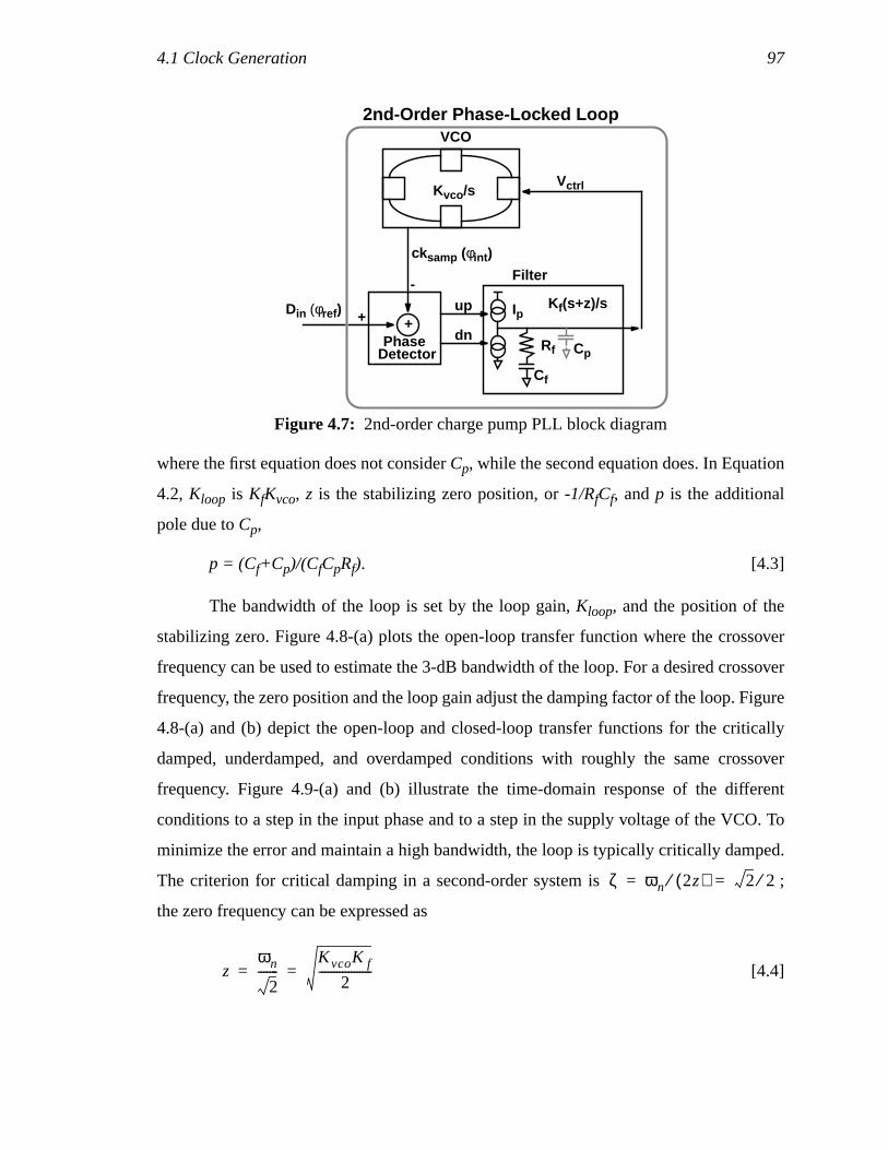
4.1 Clock Generation 97
where the first equation does not considerCp, while the second equation does. In Equation
4.2, Kloop is KfKvco, z is the stabilizing zero position, or-1/RfCf, andp is the additional
pole due toCp,
p = (Cf+Cp)/(CfCpRf). [4.3]
The bandwidth of the loop is set by the loop gain,Kloop, and the position of the
stabilizing zero. Figure 4.8-(a) plots the open-loop transfer function where the crossover
frequency can be used to estimate the 3-dB bandwidth of the loop. For a desired crossover
frequency, the zero position and the loop gain adjust the damping factor of the loop. Figure
4.8-(a) and (b) depict the open-loop and closed-loop transfer functions for the critically
damped, underdamped, and overdamped conditions with roughly the same crossover
frequency. Figure 4.9-(a) and (b) illustrate the time-domain response of the different
conditions to a step in the input phase and to a step in the supply voltage of the VCO. To
minimize the error and maintain a high bandwidth, the loop is typically critically damped.
The criterion for critical damping in a second-order system is ;
the zero frequency can be expressed as
[4.4]
Figure 4.7: 2nd-order charge pump PLL block diagram
PhaseDetector
Filter
cksamp (φint )
Din (φref)
Kvco /sVctrl
2nd-Order Phase-Locked LoopVCO
Rf
Cf
Ipup
dn++
-
Cp
Kf(s+z)/s
ζ ωn 2z( )⁄ 2 2⁄= =
zωn
2-------
KvcoK f
2------------------= =
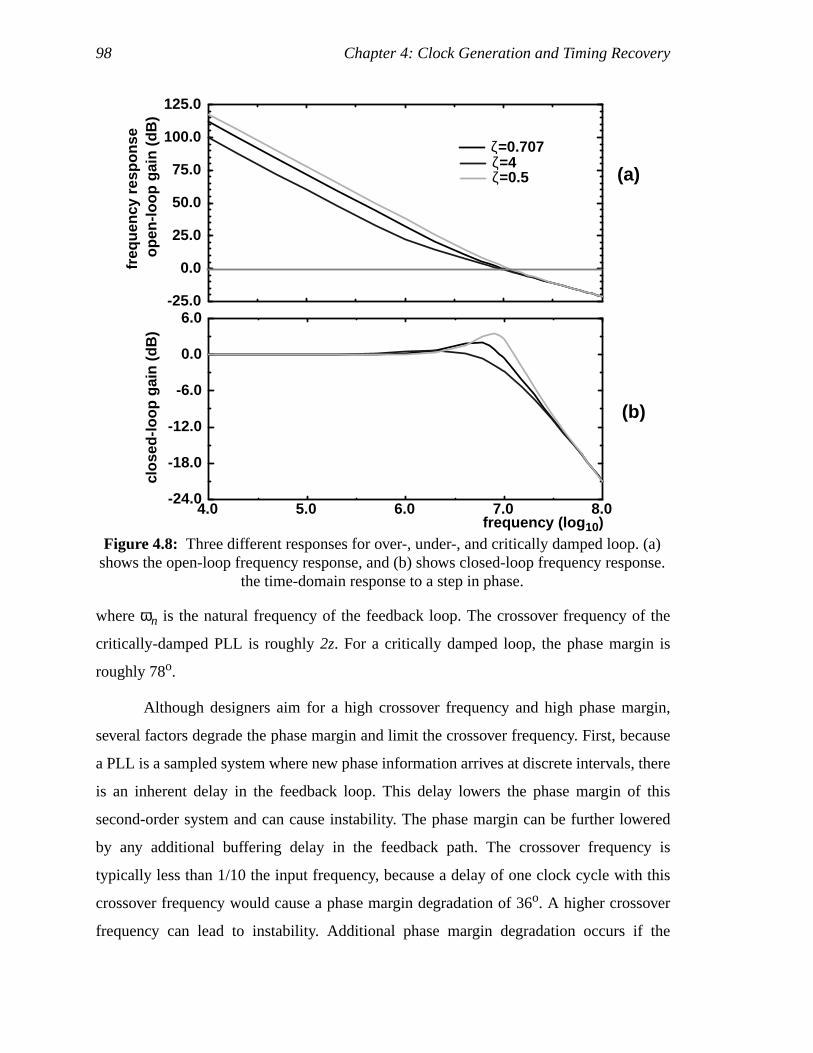
98 Chapter 4: Clock Generation and Timing Recovery
whereωn is the natural frequency of the feedback loop. The crossover frequency of the
critically-damped PLL is roughly2z. For a critically damped loop, the phase margin is
roughly 78o.
Although designers aim for a high crossover frequency and high phase margin,
several factors degrade the phase margin and limit the crossover frequency. First, because
a PLL is a sampled system where new phase information arrives at discrete intervals, there
is an inherent delay in the feedback loop. This delay lowers the phase margin of this
second-order system and can cause instability. The phase margin can be further lowered
by any additional buffering delay in the feedback path. The crossover frequency is
typically less than 1/10 the input frequency, because a delay of one clock cycle with this
crossover frequency would cause a phase margin degradation of 36o. A higher crossover
frequency can lead to instability. Additional phase margin degradation occurs if the
Figure 4.8: Three different responses for over-, under-, and critically damped loop. (a)shows the open-loop frequency response, and (b) shows closed-loop frequency response.
the time-domain response to a step in phase.
open
-loop
gai
n (d
B)
(b)
-25.0
0.0
25.0
50.0
75.0
100.0
125.0
freq
uenc
y re
spon
se
frequency (log 10)4.0 5.0 6.0 7.0 8.0
-24.0
-18.0
-12.0
-6.0
0.0
6.0
ζ=0.707ζ=4ζ=0.5
clos
ed-lo
op g
ain
(dB
)
(a)
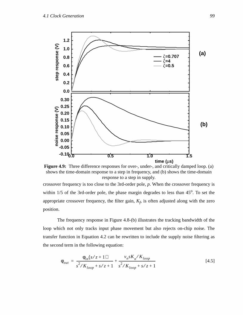
4.1 Clock Generation 99
crossover frequency is too close to the 3rd-order pole,p. When the crossover frequency is
within 1/5 of the 3rd-order pole, the phase margin degrades to less than 45o. To set the
appropriate crossover frequency, the filter gain,Kf, is often adjusted along with the zero
position.
The frequency response in Figure 4.8-(b) illustrates the tracking bandwidth of the
loop which not only tracks input phase movement but also rejects on-chip noise. The
transfer function in Equation 4.2 can be rewritten to include the supply noise filtering as
the second term in the following equation:
[4.5]
Figure 4.9: Three difference responses for over-, under-, and critically damped loop. (a)shows the time-domain response to a step in frequency, and (b) shows the time-domain
response to a step in supply.
(b)
step
res
pons
e (V
)
time ( µs)
nois
e re
spon
se (
V)
(a)
0.0
0.2
0.4
0.6
0.8
1.0
1.2
ζ=0.707ζ=4ζ=0.5
0.0 0.5 1.0 1.5-0.10
-0.05
0.00
0.05
0.10
0.15
0.20
0.25
0.30
φout
φin s z⁄ 1+( )
s2
Kloop⁄ s z⁄ 1++----------------------------------------------
vnsKn Kloop⁄
s2
Kloop⁄ s z⁄ 1++----------------------------------------------+=
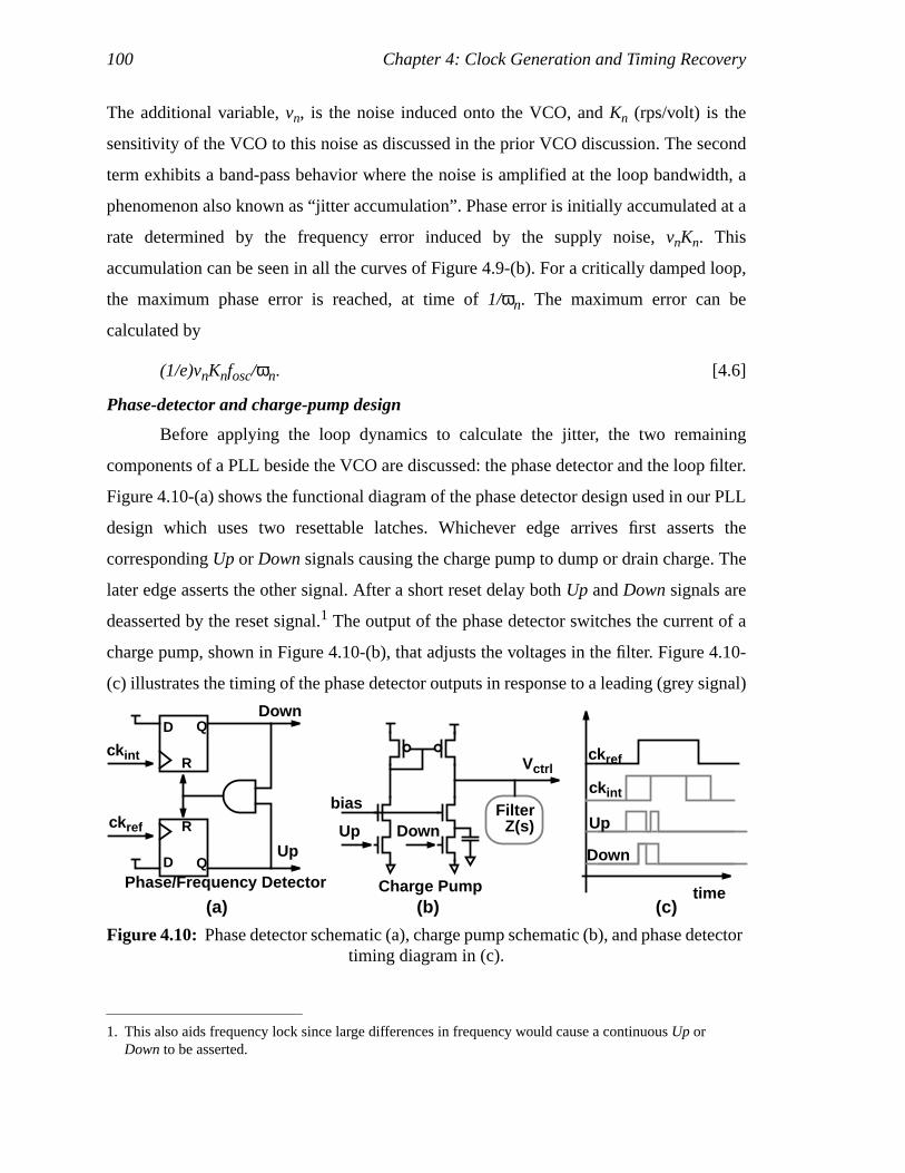
100 Chapter 4: Clock Generation and Timing Recovery
The additional variable,vn, is the noise induced onto the VCO, andKn (rps/volt) is the
sensitivity of the VCO to this noise as discussed in the prior VCO discussion. The second
term exhibits a band-pass behavior where the noise is amplified at the loop bandwidth, a
phenomenon also known as “jitter accumulation”. Phase error is initially accumulated at a
rate determined by the frequency error induced by the supply noise,vnKn. This
accumulation can be seen in all the curves of Figure 4.9-(b). For a critically damped loop,
the maximum phase error is reached, at time of1/ωn. The maximum error can be
calculated by
(1/e)vnKnfosc/ωn. [4.6]
Phase-detector and charge-pump design
Before applying the loop dynamics to calculate the jitter, the two remaining
components of a PLL beside the VCO are discussed: the phase detector and the loop filter.
Figure 4.10-(a) shows the functional diagram of the phase detector design used in our PLL
design which uses two resettable latches. Whichever edge arrives first asserts the
correspondingUp or Down signals causing the charge pump to dump or drain charge. The
later edge asserts the other signal. After a short reset delay bothUp andDown signals are
deasserted by the reset signal.1 The output of the phase detector switches the current of a
charge pump, shown in Figure 4.10-(b), that adjusts the voltages in the filter. Figure 4.10-
(c) illustrates the timing of the phase detector outputs in response to a leading (grey signal)
1. This also aids frequency lock since large differences in frequency would cause a continuousUp orDown to be asserted.
Figure 4.10: Phase detector schematic (a), charge pump schematic (b), and phase detectortiming diagram in (c).
Up
Down
ck int
ck ref
D Q
R
D Q
R Up Down
bias
Vctrl
Phase/Frequency Detector Charge Pump(a) (b)
FilterZ(s)
(c)
ck int
ck ref
Up
Down
time
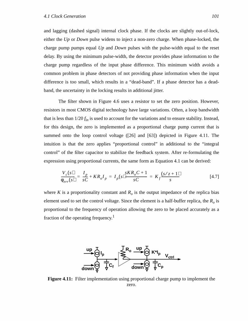
4.1 Clock Generation 101
and lagging (dashed signal) internal clock phase. If the clocks are slightly out-of-lock,
either theUp or Down pulse widens to inject a non-zero charge. When phase-locked, the
charge pump pumps equalUp andDown pulses with the pulse-width equal to the reset
delay. By using the minimum pulse-width, the detector provides phase information to the
charge pump regardless of the input phase difference. This minimum width avoids a
common problem in phase detectors of not providing phase information when the input
difference is too small, which results in a “dead-band”. If a phase detector has a dead-
band, the uncertainty in the locking results in additional jitter.
The filter shown in Figure 4.6 uses a resistor to set the zero position. However,
resistors in most CMOS digital technology have large variations. Often, a loop bandwidth
that is less than 1/20fin is used to account for the variations and to ensure stability. Instead,
for this design, the zero is implemented as a proportional charge pump current that is
summed onto the loop control voltage ([26] and [63]) depicted in Figure 4.11. The
intuition is that the zero applies “proportional control” in additional to the “integral
control” of the filter capacitor to stabilize the feedback system. After re-formulating the
expression using proportional currents, the same form as Equation 4.1 can be derived:
[4.7]
whereK is a proportionality constant andRo is the output impedance of the replica bias
element used to set the control voltage. Since the element is a half-buffer replica, theRo is
proportional to the frequency of operation allowing the zero to be placed accurately as a
fraction of the operating frequency.1
Vc s( )φerr s( )-----------------
I p
sC------ KRoI p+ I p s( )
sKRoC 1+
sC--------------------------- K f
s z⁄ 1+( )s
----------------------= = =
Figure 4.11: Filter implementation using proportional charge pump to implement thezero.
Cf
Ip K*IpRo
Cp
Vctrl
up
down
up
down
102 Chapter 4: Clock Generation and Timing Recovery
4.1.3 JitterFor the transceiver implemented in the 0.5-µm process technology with a 250-MHz input
frequency and 2x on-chip frequency multiplication, the transmitter PLL is designed to
have a loop bandwidth of roughly 15MHz (1/16 of the input frequency) with a phase
margin of 70o. The PLL for the oversampling receiver has a lower bandwidth of roughly
5MHz, 1/50 of the input frequency. These loop bandwidths can be applied to calculate the
amount of jitter contributed by the PLLs using Equation 4.6 and the supply sensitivity of
Section 4.1.1. With a 10% supply step, the peak-to-peak jitter from the PLL is 2% and 6%
of the on-chip clock period for the transmitter and receiver, respectively. With the same
supply noise, the jitter contribution of the elements following the VCO can be calculated
based on values of the prior section to be 3.7% for the transmitter and less than 1% for the
receiver. The total peak-to-peak jitter at the output of the transmitter and the sampling
clock are 5.7% and 8%, respectively. Note that these jitter numbers only indicate the noise
from the PLL clock generation. The amount that these noises degrade the timing margin
still depends on how the timing of the data is recovered.
4.2 Multiple-Phase Clock GenerationIn addition to locking the on-chip clock to an external reference, multiple phases are
needed to multiplex and demultiplex. A ring oscillator is a convenient way to generate the
multiple phases. As illustrated in Figure 4.12, eight clock phases are generated using a
four-stage ring-oscillator built with differential delay elements (four true and four
complement phases). In order for the ring to oscillate with an even number of stages, the
differential outputs of one of the stages is twisted to introduce an additional inversion.
This four-stage oscillator suffices for the clock generation for the transmitter.
1. Interestingly, the zero placement can be made to track the operating frequency if the equality ofEquation 4.4 is maintained. For the symmetric load element of the delay buffers,Kvco is roughly
constant andRo is proportional to , whereIbuf is the current through the delay element.
Therefore as long asKf is proportional toIbuf (by making the charge pump current proportional to
Ibuf), the loop stability is guaranteed for a wide frequency range.[63]
1 I buf( )⁄
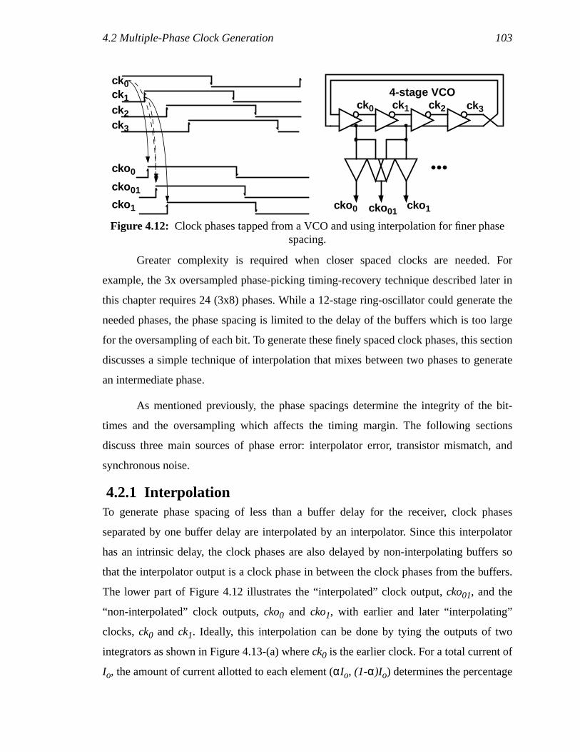
4.2 Multiple-Phase Clock Generation 103
Greater complexity is required when closer spaced clocks are needed. For
example, the 3x oversampled phase-picking timing-recovery technique described later in
this chapter requires 24 (3x8) phases. While a 12-stage ring-oscillator could generate the
needed phases, the phase spacing is limited to the delay of the buffers which is too large
for the oversampling of each bit. To generate these finely spaced clock phases, this section
discusses a simple technique of interpolation that mixes between two phases to generate
an intermediate phase.
As mentioned previously, the phase spacings determine the integrity of the bit-
times and the oversampling which affects the timing margin. The following sections
discuss three main sources of phase error: interpolator error, transistor mismatch, and
synchronous noise.
4.2.1 InterpolationTo generate phase spacing of less than a buffer delay for the receiver, clock phases
separated by one buffer delay are interpolated by an interpolator. Since this interpolator
has an intrinsic delay, the clock phases are also delayed by non-interpolating buffers so
that the interpolator output is a clock phase in between the clock phases from the buffers.
The lower part of Figure 4.12 illustrates the “interpolated” clock output,cko01, and the
“non-interpolated” clock outputs,cko0 and cko1, with earlier and later “interpolating”
clocks,ck0 andck1. Ideally, this interpolation can be done by tying the outputs of two
integrators as shown in Figure 4.13-(a) whereck0 is the earlier clock. For a total current of
Io, the amount of current allotted to each element (αIo, (1-α)Io) determines the percentage
Figure 4.12: Clock phases tapped from a VCO and using interpolation for finer phasespacing.
ck0ck1ck2ck3
4-stage VCOck0 ck1 ck2 ck3
cko 0 cko 01cko 1
cko 0
cko 1
cko 01
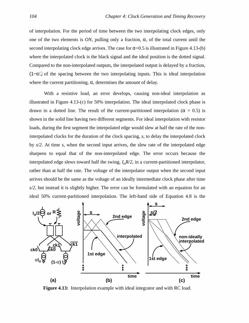
104 Chapter 4: Clock Generation and Timing Recovery
of interpolation. For the period of time between the two interpolating clock edges, only
one of the two elements isON, pulling only a fraction,α, of the total current until the
second interpolating clock edge arrives. The case forα=0.5 is illustrated in Figure 4.13-(b)
where the interpolated clock is the black signal and the ideal position is the dotted signal.
Compared to the non-interpolated outputs, the interpolated output is delayed by a fraction,
(1−α), of the spacing between the two interpolating inputs. This is ideal interpolation
where the current partitioning,α, determines the amount of delay.
With a resistive load, an error develops, causing non-ideal interpolation as
illustrated in Figure 4.13-(c) for 50% interpolation. The ideal interpolated clock phase is
drawn in a dotted line. The result of the current-partitioned interpolation (α = 0.5) is
shown in the solid line having two different segments. For ideal interpolation with resistor
loads, during the first segment the interpolated edge would slew at half the rate of the non-
interpolated clocks for the duration of the clock spacing,s, to delay the interpolated clock
by s/2. At time s, when the second input arrives, the slew rate of the interpolated edge
sharpens to equal that of the non-interpolated edge. The error occurs because the
interpolated edge slews toward half the swing,IoR/2, in a current-partitioned interpolator,
rather than at half the rate. The voltage of the interpolator output when the second input
arrives should be the same as the voltage of an ideally intermediate clock phase after time
s/2, but instead it is slightly higher. The error can be formulated with an equation for an
ideal 50% current-partitioned interpolation. The left-hand side of Equation 4.8 is the
Figure 4.13: Interpolation example with ideal integrator and with RC load.
(a)
2nd edge
1st edge
interpolated
volta
ge
time(b)
2nd edge
1st edge
non-ideally
volta
ge
time
s
s
s/2
αIo (1-α) Io
Io/2
ck0ck1
ck0ck1
(c)
interpolated
Ror
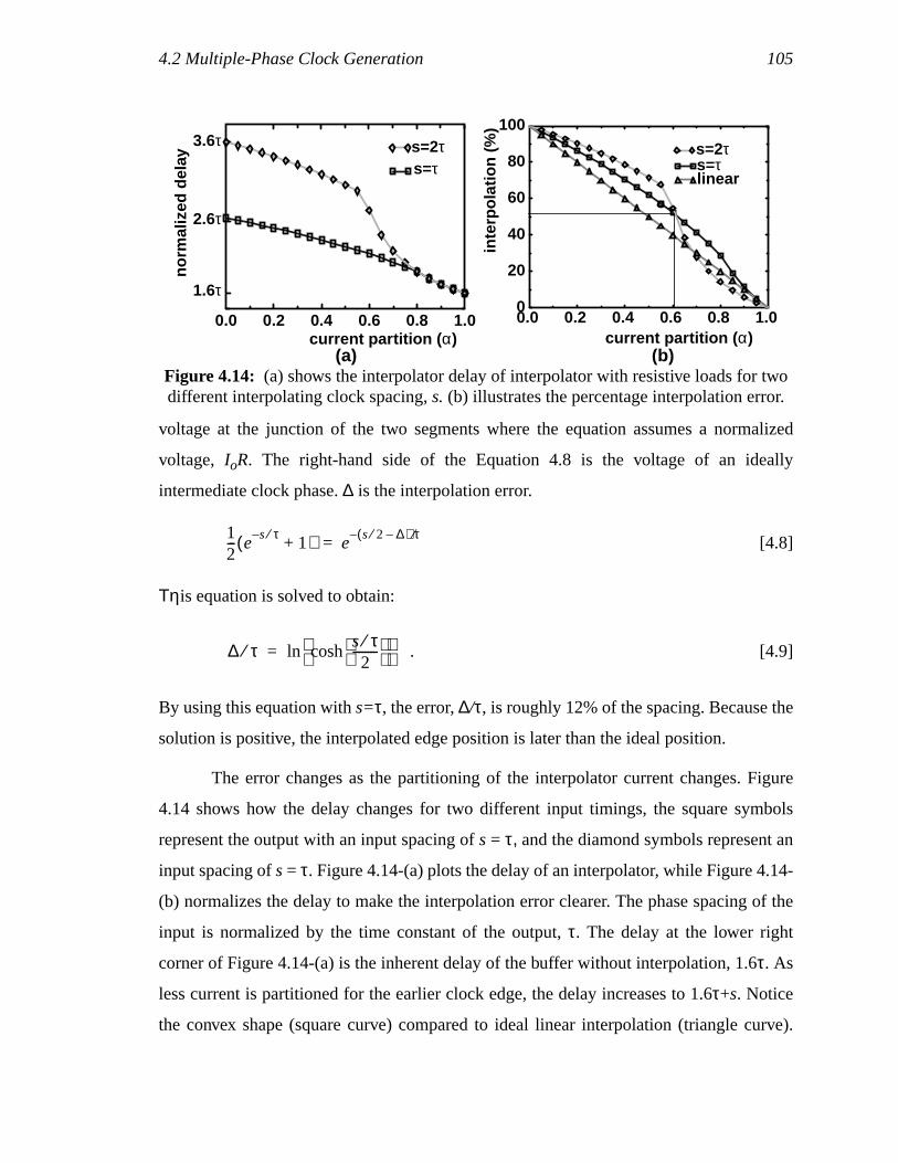
4.2 Multiple-Phase Clock Generation 105
voltage at the junction of the two segments where the equation assumes a normalized
voltage, IoR. The right-hand side of the Equation 4.8 is the voltage of an ideally
intermediate clock phase.∆ is the interpolation error.
[4.8]
Τηis equation is solved to obtain:
. [4.9]
By using this equation withs=τ, the error,∆/τ, is roughly 12% of the spacing. Because the
solution is positive, the interpolated edge position is later than the ideal position.
The error changes as the partitioning of the interpolator current changes. Figure
4.14 shows how the delay changes for two different input timings, the square symbols
represent the output with an input spacing ofs = τ, and the diamond symbols represent an
input spacing ofs = τ. Figure 4.14-(a) plots the delay of an interpolator, while Figure 4.14-
(b) normalizes the delay to make the interpolation error clearer. The phase spacing of the
input is normalized by the time constant of the output,τ. The delay at the lower right
corner of Figure 4.14-(a) is the inherent delay of the buffer without interpolation, 1.6τ. As
less current is partitioned for the earlier clock edge, the delay increases to 1.6τ+s. Notice
the convex shape (square curve) compared to ideal linear interpolation (triangle curve).
12--- e
s τ⁄–1+( ) e
s 2⁄ ∆–( ) τ⁄–=
∆ τ⁄ s τ⁄2
-------- cosh
ln=
Figure 4.14: (a) shows the interpolator delay of interpolator with resistive loads for twodifferent interpolating clock spacing,s. (b) illustrates the percentage interpolation error.
0.0 0.2 0.4 0.6 0.8 1.00
20
40
60
80
100
s=τs=2τ
linear
0.0 0.2 0.4 0.6 0.8 1.0
1.6τ
2.6τ
3.6τ
s=τs=2τ
current partition ( α)
norm
aliz
ed d
elay
current partition ( α)
inte
rpol
atio
n (%
)
(a) (b)
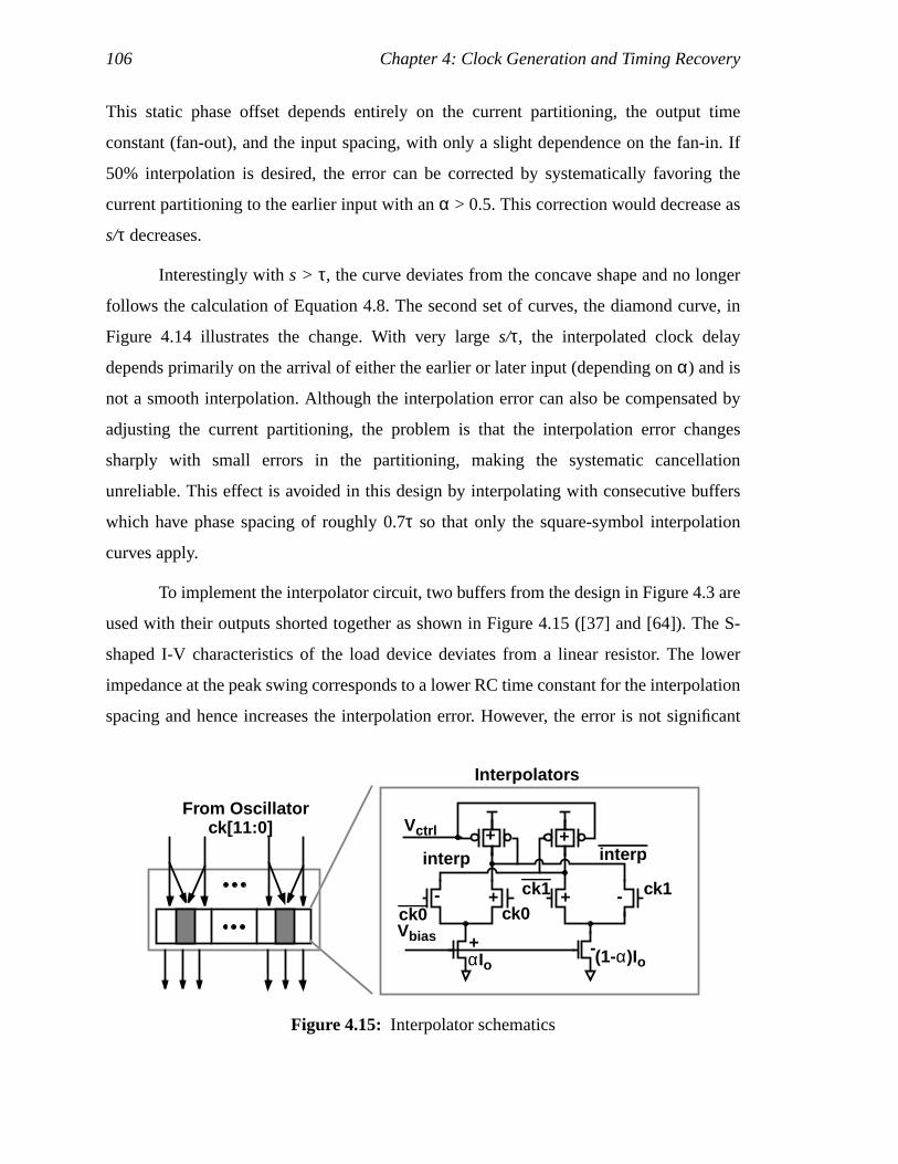
106 Chapter 4: Clock Generation and Timing Recovery
This static phase offset depends entirely on the current partitioning, the output time
constant (fan-out), and the input spacing, with only a slight dependence on the fan-in. If
50% interpolation is desired, the error can be corrected by systematically favoring the
current partitioning to the earlier input with anα > 0.5. This correction would decrease as
s/τ decreases.
Interestingly withs > τ, the curve deviates from the concave shape and no longer
follows the calculation of Equation 4.8. The second set of curves, the diamond curve, in
Figure 4.14 illustrates the change. With very larges/τ, the interpolated clock delay
depends primarily on the arrival of either the earlier or later input (depending onα) and is
not a smooth interpolation. Although the interpolation error can also be compensated by
adjusting the current partitioning, the problem is that the interpolation error changes
sharply with small errors in the partitioning, making the systematic cancellation
unreliable. This effect is avoided in this design by interpolating with consecutive buffers
which have phase spacing of roughly 0.7τ so that only the square-symbol interpolation
curves apply.
To implement the interpolator circuit, two buffers from the design in Figure 4.3 are
used with their outputs shorted together as shown in Figure 4.15 ([37] and [64]). The S-
shaped I-V characteristics of the load device deviates from a linear resistor. The lower
impedance at the peak swing corresponds to a lower RC time constant for the interpolation
spacing and hence increases the interpolation error. However, the error is not significant
Figure 4.15: Interpolator schematics
Interpolators
ck[11:0]
ck0
ck1 ck1ck0
interp interp
Vctrl
Vbias
(1-α)Io
+ +
+ + --
-+αIo
From Oscillator
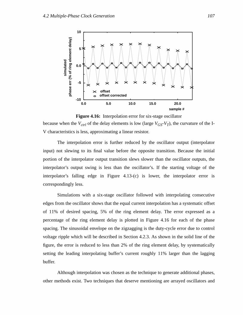
4.2 Multiple-Phase Clock Generation 107
because when theVctrl of the delay elements is low (largeVGS-VT), the curvature of the I-
V characteristics is less, approximating a linear resistor.
The interpolation error is further reduced by the oscillator output (interpolator
input) not slewing to its final value before the opposite transition. Because the initial
portion of the interpolator output transition slews slower than the oscillator outputs, the
interpolator’s output swing is less than the oscillator’s. If the starting voltage of the
interpolator’s falling edge in Figure 4.13-(c) is lower, the interpolator error is
correspondingly less.
Simulations with a six-stage oscillator followed with interpolating consecutive
edges from the oscillator shows that the equal current interpolation has a systematic offset
of 11% of desired spacing, 5% of the ring element delay. The error expressed as a
percentage of the ring element delay is plotted in Figure 4.16 for each of the phase
spacing. The sinusoidal envelope on the zigzagging is the duty-cycle error due to control
voltage ripple which will be described in Section 4.2.3. As shown in the solid line of the
figure, the error is reduced to less than 2% of the ring element delay, by systematically
setting the leading interpolating buffer’s current roughly 11% larger than the lagging
buffer.
Although interpolation was chosen as the technique to generate additional phases,
other methods exist. Two techniques that deserve mentioning are arrayed oscillators and
Figure 4.16: Interpolation error for six-stage oscillator
phas
e er
r (%
of r
ing
elem
ent d
elay
)
sample #
0.0 10.0 20.0-10
-5
0.0
5
10
offsetoffset corrected
sim
ulat
ed
5.0 15.0
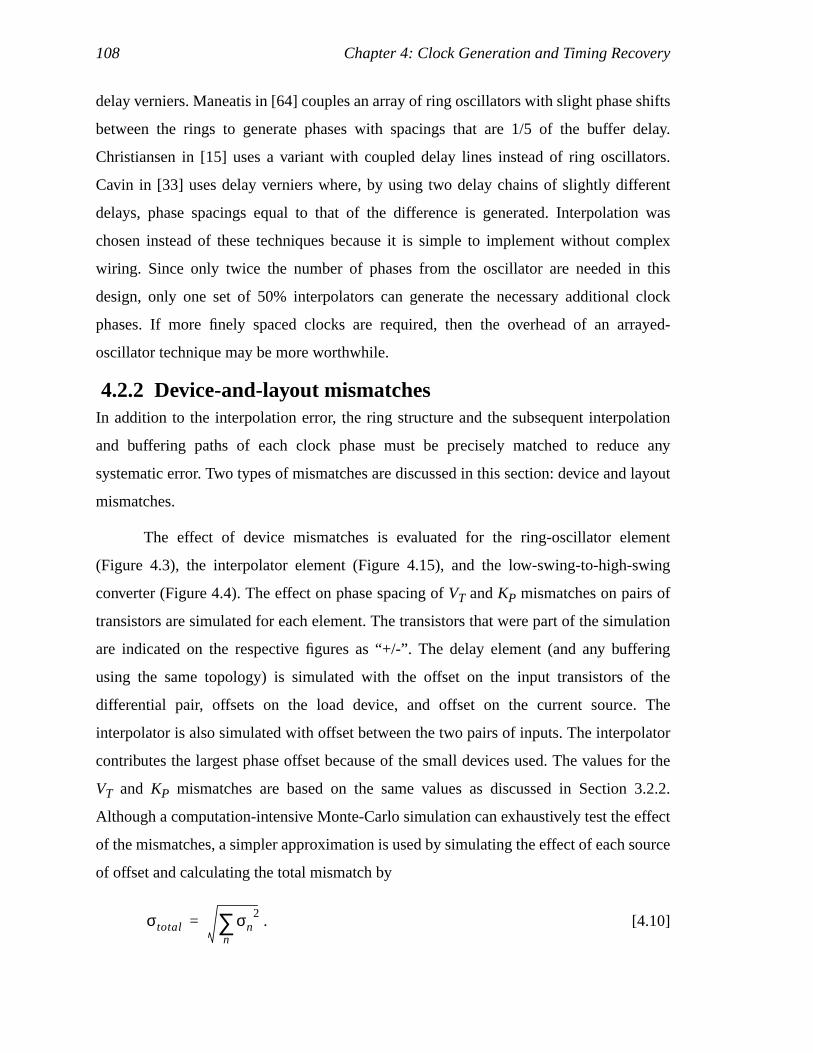
108 Chapter 4: Clock Generation and Timing Recovery
delay verniers. Maneatis in [64] couples an array of ring oscillators with slight phase shifts
between the rings to generate phases with spacings that are 1/5 of the buffer delay.
Christiansen in [15] uses a variant with coupled delay lines instead of ring oscillators.
Cavin in [33] uses delay verniers where, by using two delay chains of slightly different
delays, phase spacings equal to that of the difference is generated. Interpolation was
chosen instead of these techniques because it is simple to implement without complex
wiring. Since only twice the number of phases from the oscillator are needed in this
design, only one set of 50% interpolators can generate the necessary additional clock
phases. If more finely spaced clocks are required, then the overhead of an arrayed-
oscillator technique may be more worthwhile.
4.2.2 Device-and-layout mismatchesIn addition to the interpolation error, the ring structure and the subsequent interpolation
and buffering paths of each clock phase must be precisely matched to reduce any
systematic error. Two types of mismatches are discussed in this section: device and layout
mismatches.
The effect of device mismatches is evaluated for the ring-oscillator element
(Figure 4.3), the interpolator element (Figure 4.15), and the low-swing-to-high-swing
converter (Figure 4.4). The effect on phase spacing ofVT andKP mismatches on pairs of
transistors are simulated for each element. The transistors that were part of the simulation
are indicated on the respective figures as “+/-”. The delay element (and any buffering
using the same topology) is simulated with the offset on the input transistors of the
differential pair, offsets on the load device, and offset on the current source. The
interpolator is also simulated with offset between the two pairs of inputs. The interpolator
contributes the largest phase offset because of the small devices used. The values for the
VT and KP mismatches are based on the same values as discussed in Section 3.2.2.
Although a computation-intensive Monte-Carlo simulation can exhaustively test the effect
of the mismatches, a simpler approximation is used by simulating the effect of each source
of offset and calculating the total mismatch by
. [4.10]σtotal σn2
n∑=
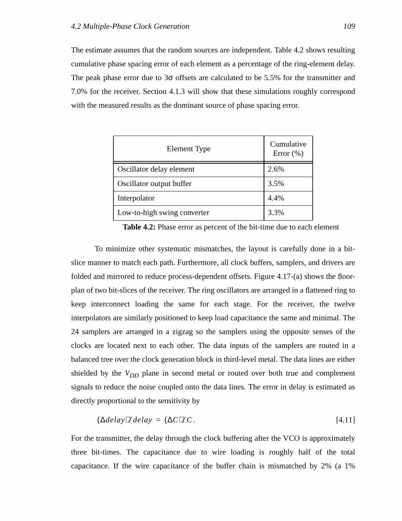
4.2 Multiple-Phase Clock Generation 109
The estimate assumes that the random sources are independent. Table 4.2 shows resulting
cumulative phase spacing error of each element as a percentage of the ring-element delay.
The peak phase error due to 3σ offsets are calculated to be 5.5% for the transmitter and
7.0% for the receiver. Section 4.1.3 will show that these simulations roughly correspond
with the measured results as the dominant source of phase spacing error.
To minimize other systematic mismatches, the layout is carefully done in a bit-
slice manner to match each path. Furthermore, all clock buffers, samplers, and drivers are
folded and mirrored to reduce process-dependent offsets. Figure 4.17-(a) shows the floor-
plan of two bit-slices of the receiver. The ring oscillators are arranged in a flattened ring to
keep interconnect loading the same for each stage. For the receiver, the twelve
interpolators are similarly positioned to keep load capacitance the same and minimal. The
24 samplers are arranged in a zigzag so the samplers using the opposite senses of the
clocks are located next to each other. The data inputs of the samplers are routed in a
balanced tree over the clock generation block in third-level metal. The data lines are either
shielded by theVDD plane in second metal or routed over both true and complement
signals to reduce the noise coupled onto the data lines. The error in delay is estimated as
directly proportional to the sensitivity by
. [4.11]
For the transmitter, the delay through the clock buffering after the VCO is approximately
three bit-times. The capacitance due to wire loading is roughly half of the total
capacitance. If the wire capacitance of the buffer chain is mismatched by 2% (a 1%
Element TypeCumulativeError (%)
Oscillator delay element 2.6%
Oscillator output buffer 3.5%
Interpolator 4.4%
Low-to-high swing converter 3.3%
Table 4.2:Phase error as percent of the bit-time due to each element
∆delay( ) delay⁄ ∆C( ) C⁄=
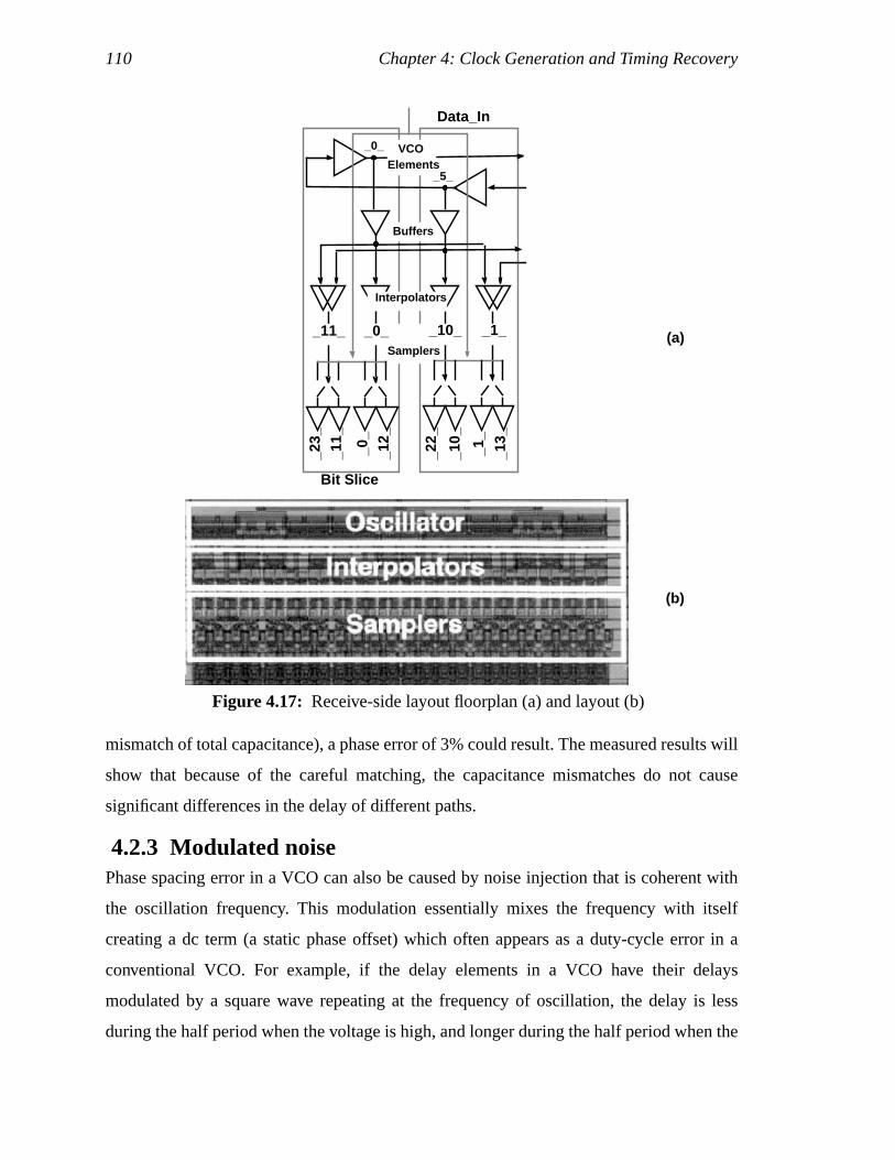
110 Chapter 4: Clock Generation and Timing Recovery
mismatch of total capacitance), a phase error of 3% could result. The measured results will
show that because of the careful matching, the capacitance mismatches do not cause
significant differences in the delay of different paths.
4.2.3 Modulated noisePhase spacing error in a VCO can also be caused by noise injection that is coherent with
the oscillation frequency. This modulation essentially mixes the frequency with itself
creating a dc term (a static phase offset) which often appears as a duty-cycle error in a
conventional VCO. For example, if the delay elements in a VCO have their delays
modulated by a square wave repeating at the frequency of oscillation, the delay is less
during the half period when the voltage is high, and longer during the half period when the
Figure 4.17: Receive-side layout floorplan (a) and layout (b)
_5_
_11_ _0_ _10_ _1_
_0_
_1_
_11_
_10_
_12_
_13_
_23_
_22_
Data_In
Bit Slice
_0_
Buffers
VCOElements
Interpolators
Samplers(a)
(b)
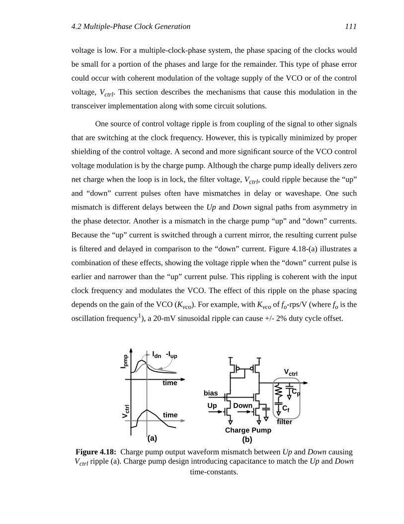
4.2 Multiple-Phase Clock Generation 111
voltage is low. For a multiple-clock-phase system, the phase spacing of the clocks would
be small for a portion of the phases and large for the remainder. This type of phase error
could occur with coherent modulation of the voltage supply of the VCO or of the control
voltage,Vctrl. This section describes the mechanisms that cause this modulation in the
transceiver implementation along with some circuit solutions.
One source of control voltage ripple is from coupling of the signal to other signals
that are switching at the clock frequency. However, this is typically minimized by proper
shielding of the control voltage. A second and more significant source of the VCO control
voltage modulation is by the charge pump. Although the charge pump ideally delivers zero
net charge when the loop is in lock, the filter voltage,Vctrl, could ripple because the “up”
and “down” current pulses often have mismatches in delay or waveshape. One such
mismatch is different delays between theUp andDown signal paths from asymmetry in
the phase detector. Another is a mismatch in the charge pump “up” and “down” currents.
Because the “up” current is switched through a current mirror, the resulting current pulse
is filtered and delayed in comparison to the “down” current. Figure 4.18-(a) illustrates a
combination of these effects, showing the voltage ripple when the “down” current pulse is
earlier and narrower than the “up” current pulse. This rippling is coherent with the input
clock frequency and modulates the VCO. The effect of this ripple on the phase spacing
depends on the gain of the VCO (Kvco). For example, withKvco of fo-rps/V (wherefo is the
oscillation frequency1), a 20-mV sinusoidal ripple can cause +/- 2% duty cycle offset.
Figure 4.18: Charge pump output waveform mismatch betweenUp andDown causingVctrl ripple (a). Charge pump design introducing capacitance to match theUp andDown
time-constants.
Up Down
bias
Vctrl
Charge Pump(b)
filter
Cp
Cf
I pm
pV
ctrl
time
Idn -Iup
time
(a)
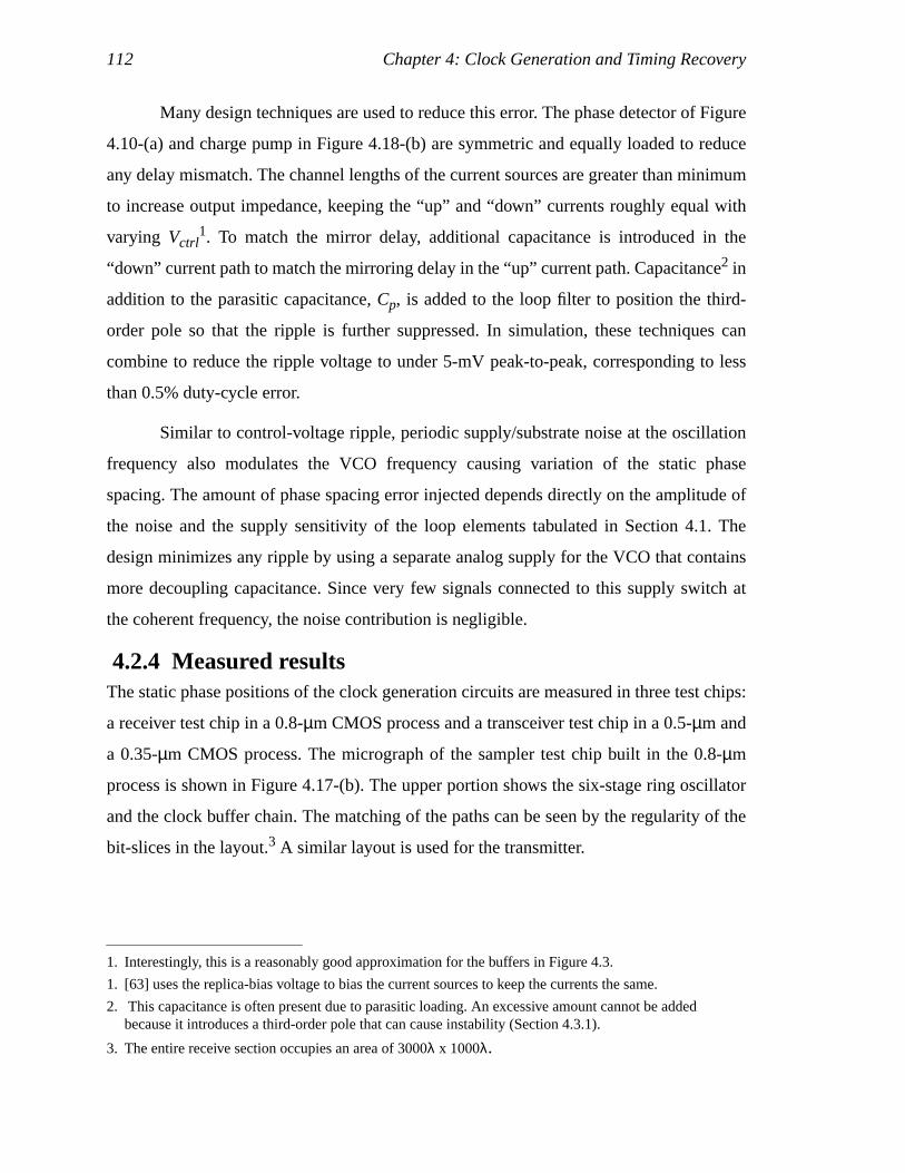
112 Chapter 4: Clock Generation and Timing Recovery
Many design techniques are used to reduce this error. The phase detector of Figure
4.10-(a) and charge pump in Figure 4.18-(b) are symmetric and equally loaded to reduce
any delay mismatch. The channel lengths of the current sources are greater than minimum
to increase output impedance, keeping the “up” and “down” currents roughly equal with
varying Vctrl1. To match the mirror delay, additional capacitance is introduced in the
“down” current path to match the mirroring delay in the “up” current path. Capacitance2 in
addition to the parasitic capacitance,Cp, is added to the loop filter to position the third-
order pole so that the ripple is further suppressed. In simulation, these techniques can
combine to reduce the ripple voltage to under 5-mV peak-to-peak, corresponding to less
than 0.5% duty-cycle error.
Similar to control-voltage ripple, periodic supply/substrate noise at the oscillation
frequency also modulates the VCO frequency causing variation of the static phase
spacing. The amount of phase spacing error injected depends directly on the amplitude of
the noise and the supply sensitivity of the loop elements tabulated in Section 4.1. The
design minimizes any ripple by using a separate analog supply for the VCO that contains
more decoupling capacitance. Since very few signals connected to this supply switch at
the coherent frequency, the noise contribution is negligible.
4.2.4 Measured resultsThe static phase positions of the clock generation circuits are measured in three test chips:
a receiver test chip in a 0.8-µm CMOS process and a transceiver test chip in a 0.5-µm and
a 0.35-µm CMOS process. The micrograph of the sampler test chip built in the 0.8-µm
process is shown in Figure 4.17-(b). The upper portion shows the six-stage ring oscillator
and the clock buffer chain. The matching of the paths can be seen by the regularity of the
bit-slices in the layout.3 A similar layout is used for the transmitter.
1. Interestingly, this is a reasonably good approximation for the buffers in Figure 4.3.
1. [63] uses the replica-bias voltage to bias the current sources to keep the currents the same.
2. This capacitance is often present due to parasitic loading. An excessive amount cannot be addedbecause it introduces a third-order pole that can cause instability (Section 4.3.1).
3. The entire receive section occupies an area of 3000λ x 1000λ.
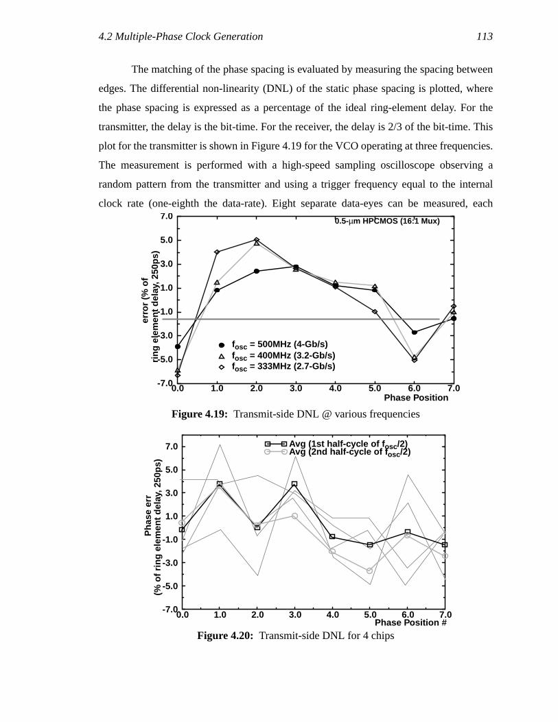
4.2 Multiple-Phase Clock Generation 113
The matching of the phase spacing is evaluated by measuring the spacing between
edges. The differential non-linearity (DNL) of the static phase spacing is plotted, where
the phase spacing is expressed as a percentage of the ideal ring-element delay. For the
transmitter, the delay is the bit-time. For the receiver, the delay is 2/3 of the bit-time. This
plot for the transmitter is shown in Figure 4.19 for the VCO operating at three frequencies.
The measurement is performed with a high-speed sampling oscilloscope observing a
random pattern from the transmitter and using a trigger frequency equal to the internal
clock rate (one-eighth the data-rate). Eight separate data-eyes can be measured, each
Figure 4.19: Transmit-side DNL @ various frequencies
0.0 1.0 2.0 3.0 4.0 5.0 6.0 7.0-7.0
-5.0
-3.0
-1.0
1.0
3.0
5.0
7.0
fosc = 500MHz (4-Gb/s)fosc = 400MHz (3.2-Gb/s)fosc = 333MHz (2.7-Gb/s)
Phase Position
erro
r (%
of
0.5-µm HPCMOS (16:1 Mux)
ring
elem
ent d
elay
, 250
ps)
Figure 4.20: Transmit-side DNL for 4 chipsPhase Position #
0.0 1.0 2.0 3.0 4.0 5.0 6.0 7.0-7.0
-5.0
-3.0
-1.0
1.0
3.0
5.0
7.0 Avg (1st half-cycle of f osc /2)Avg (2nd half-cycle of f osc /2)
Pha
se e
rr(%
of r
ing
elem
ent d
elay
, 250
ps)
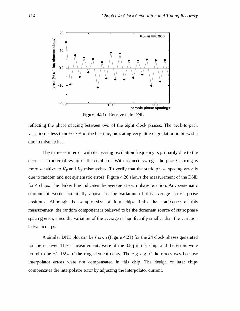
114 Chapter 4: Clock Generation and Timing Recovery
reflecting the phase spacing between two of the eight clock phases. The peak-to-peak
variation is less than +/- 7% of the bit-time, indicating very little degradation in bit-width
due to mismatches.
The increase in error with decreasing oscillation frequency is primarily due to the
decrease in internal swing of the oscillator. With reduced swings, the phase spacing is
more sensitive toVT andKP mismatches. To verify that the static phase spacing error is
due to random and not systematic errors, Figure 4.20 shows the measurement of the DNL
for 4 chips. The darker line indicates the average at each phase position. Any systematic
component would potentially appear as the variation of this average across phase
positions. Although the sample size of four chips limits the confidence of this
measurement, the random component is believed to be the dominant source of static phase
spacing error, since the variation of the average is significantly smaller than the variation
between chips.
A similar DNL plot can be shown (Figure 4.21) for the 24 clock phases generated
for the receiver. These measurements were of the 0.8-µm test chip, and the errors were
found to be +/- 13% of the ring element delay. The zig-zag of the errors was because
interpolator errors were not compensated in this chip. The design of later chips
compensates the interpolator error by adjusting the interpolator current.
Figure 4.21: Receive-side DNL
0.0 10.0 20.0-20
-10
0.0
10
20
sample phase spacing#
erro
r (%
of r
ing
elem
ent d
elay
)
0.8-µm HPCMOS
4.3 Timing-Recovery Architectures 115
4.2.5 SummaryBased on both the simulation and measurement results, static phase error due to
modulated noise is small enough that it will not significantly affect performance. The
primary source of error is due to device or capacitance mismatch. The errors inherent in
the interpolation and due to modulation of the oscillation frequency can both be
systematically corrected with careful design. The total static phase error has been
measured to be less than 10% of the ring element delay. This error is sufficiently small to
allow the 8x multiplexing and demultiplexing. However, with the smaller feature sizes of
future process technologies, the device mismatches increase and can become a more
significant effect. Future circuits therefore might need some method of calibrating the
clock spacing.
4.3 Timing-Recovery ArchitecturesThe previous section demonstrated that precisely-spaced multiple clock phases can be
generated. This section describes how to align the clock to the incoming data in the
receiver. The task of the timing-recovery circuit is to recover the phase-and-frequency
information from the input by extracting the clock from the transitions in the data stream.
The optimal sample point is midway between the possible data-transition times. Noise and
mismatches inherent to the timing-recovery circuit introduce jitter and static phase offset
in the sampling clocks, which degrade the timing margin. Moreover, this clock extraction
is made more difficult by transmitter jitter which introduces uncertainty in the transition
points that the timing-recovery circuit must filter or track.
Two timing-recovery architectures have been proposed: directly aligning the PLL
outputs to the data (data-recovery PLL) or phase-picking. A data-recovery PLL uses the
same PLL described for the multiple phase clock generation (Section 4.1), except the
phase detector must now use the input data and not an external clock. In a phase-picking
architecture, the data is oversampled at multiple-phase positions. Based on the phase
information in the data, the best sample is chosen as the data bit by some decision logic.
The primary difference between the architectures is the tracking rate. The PLL has
a finite loop bandwidth due to stability issues in the feedback loop while the phase-picking
116 Chapter 4: Clock Generation and Timing Recovery
architecture does not use feedback and can respond at the rate of the decision logic. As
discussed in Section 4.1.2, the bandwidth at which the input is tracked affects the jitter
performance. It is very important for the tracking rate to be greater than the bandwidth of
the PLL at the transmitter because noise on the transmitter VCO is accumulated by the
VCO at its loop bandwidth. If the receiver-PLL bandwidth is less than that of the
transmitter, the transmitter phase noise would appear as peak-to-peak timing error at the
receiver.1 The next two sections explore these two methods in more detail, and show that
although phase-picking has worse area and static offsets, it has a much higher tracking rate
which can be more robust to jitter.
4.3.1 Phase-locked loop-based timing recoveryTo maintain a large timing margin, the sampling clock phase must be locked to the center
of the input data-eye by the PLL. To maintain a good phase relationship between the
sampling clocks and the data transitions, ideally the PLL should detect the input phase
accurately and track any input jitter with a high loop bandwidth. Unfortunately, loop
stability limits the tracking bandwidth of these systems. This section first discusses the
loop-bandwidth constraints and then describes methods of phase detection.
Because the timing information is embedded in the data stream, coding of the
channel is used to ensure a minimum and maximum transition density. Thus, this coding
sets the minimum and maximum input rate to the data-recovery PLL since the PLL can
only measure phase error when an input transition occurs. A line-coding scheme such as
8B/10B [100] is often used. This guarantees greater than one transition every five bits of
data. Although this penalizes the data rate by 20%, it restricts the input-frequency
spectrum to a range of five. Furthermore, the transition coding guarantees the data stream
to be dc-balanced which allows ac-coupling of the signal.
Loop bandwidth
The analysis of loop stability in Section 4.1 is still applicable to loops with varying
input frequencies. OnlyIp, which is defined to beIpump/2πfin, increases with decreasing
1. The averaging of the receiver timing recovery would make the timing-margin degradation equal tohalf of the peak-to-peak jitter.
4.3 Timing-Recovery Architectures 117
input frequency, which in turn increases the loop gain. The loop bandwidth must be
sufficiently low so that even with the maximum loop gain, the loop remains stable.
However, this implies that the loop is no longer critically damped for all input frequencies.
Typically it is designed to be critically damped for high input frequency, and overdamped
for low input frequencies.1
Since the 8B/10B coding guarantees one transition every byte, the input frequency
is similar to the on-chip clock frequency of an 1:8 demultiplexed system. Thus, the
maximum loop bandwidth of the data-recovery PLL can potentially be similar to the
earlier transmitter PLL (Section 4.1) at a value less than 1/10 of the input frequency.
Phase detection
The phase detector measures the relative phase between the sampling clock and the
data transition in order to center the sampling edge in the middle of the data eye. The
phase detector must first use the sampled data to find data transitions before determining
the phase difference. As discussed in Chapter 2, static phase error results from errors in
the phase detector or charge pump. The following paragraphs first discuss a common
phase detector that has been used for lower data rates. Then, an alternative approach for
higher data rates is discussed.
A common technique for non-demultiplexed receiver is Hogge’s phase detector [7]
as shown in Figure 4.22 (which has variants such as a tri-wave detector [57] and was
recently adapted for 2x demultiplexing by Nakamura in [73]). Data transitions are
detected using XORs.XORA always outputs a pulse for half the bit-time (π radians)
whenever a transition is detected. The half bit-time is guaranteed by taking the inputs from
two latches clocked with opposite clock phases.XORB outputs a pulse that is wider or
narrower depending on the phase relationship of the clock compared to the data transition.
The difference in the two pulses fed into a charge pump results in a net “up” or “down”
charge.
1. An interesting aside is that to maintain stability for all input frequencies, the third-order polefrequency due to Cp must be much higher than the loop bandwidth. The ripple on the control voltage
can not be filtered. For a multiple phased system, this can potentially cause significant phase spacingerrors if the frequency range of the input is not constrained.
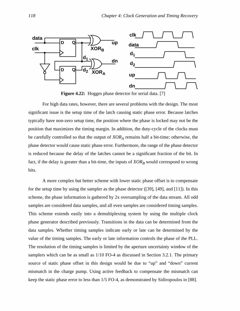
118 Chapter 4: Clock Generation and Timing Recovery
For high data rates, however, there are several problems with the design. The most
significant issue is the setup time of the latch causing static phase error. Because latches
typically have non-zero setup time, the position where the phase is locked may not be the
position that maximizes the timing margin. In addition, the duty-cycle of the clocks must
be carefully controlled so that the output ofXORA remains half a bit-time; otherwise, the
phase detector would cause static phase error. Furthermore, the range of the phase detector
is reduced because the delay of the latches cannot be a significant fraction of the bit. In
fact, if the delay is greater than a bit-time, the inputs ofXORB would correspond to wrong
bits.
A more complex but better scheme with lower static phase offset is to compensate
for the setup time by using the sampler as the phase detector ([39], [49], and [11]). In this
scheme, the phase information is gathered by 2x oversampling of the data stream. All odd
samples are considered data samples, and all even samples are considered timing samples.
This scheme extends easily into a demultiplexing system by using the multiple clock
phase generator described previously. Transitions in the data can be determined from the
data samples. Whether timing samples indicate early or late can be determined by the
value of the timing samples. The early or late information controls the phase of the PLL.
The resolution of the timing samples is limited by the aperture uncertainty window of the
samplers which can be as small as 1/10 FO-4 as discussed in Section 3.2.1. The primary
source of static phase offset in this design would be due to “up” and “down” current
mismatch in the charge pump. Using active feedback to compensate the mismatch can
keep the static phase error to less than 1/5 FO-4, as demonstrated by Sidiropoulos in [88].
Figure 4.22: Hogges phase detector for serial data. [7]
dataup
dn
clkD Q
D Q XORA
XORB
d1
d2
data
up
dn
clk
d1
d2
4.3 Timing-Recovery Architectures 119
There are several difficulties in using this phase detector. One is the additional
digital processing necessary to determine transitions. The processing delay adds to the
delay of the feedback loop and reduces the phase margin of the loop. A second issue is that
since the timing sample is at the data transition, the sampler output must be properly
synchronized by additional latches to reduce the metastability probability. This
synchronization delay further increases the delay of the feedback loop by several clock
cycles. A third issue is that the sampler phase detector is a non-linear phase detector. The
sampler either indicates “up” or “down” depending on whether the transition is early or
late without any indication of the magnitude of the error. This type of “bang-bang control”
has inherent dithering near lock increasing the jitter. To maintain stability, PLL designers
must choose a loop bandwidth much lower than 1/10 of the input frequency. A design, by
Hu in [39], uses a loop bandwidth less than 1/500 the minimum data frequency.
Moreover, a problem with any detector that only detects phase is that a frequency
acquisition aid is needed in order to phase lock when the circuit starts up. Otherwise, the
PLL could continually “cycle-slip” [7]. One possible solution employs an alternate circuit
such as the phase/frequency detector of Figure 4.10-(a) during an initialization sequence
to push the frequency near lock before switching to the sampler as the phase detector.
Clever techniques to safely lock and maintain stability is an interesting area of further
research.
Building a data-recovery PLL is possible but difficult at high data rates. The
primary challenges are maintaining small static phase error and dynamic phase error
between the data and the sampling clock. Static phase offset smaller than 1/5 FO-4 can be
achieved using 2x oversampling as long as the designer is careful with mismatches in the
phase detector and charge pump. The more difficult problem is maintaining low dynamic
phase errors while using samplers as phase detectors. The longer processing delay, the
synchronization delay, and the non-linearity of the phase detector require a lower loop
bandwidth to maintain stability. A low bandwidth may be sufficient if the phase noise
from the transmitter and receiver is at a low frequency. For noise at high frequencies, the
next section describes a solution that provides faster tracking.
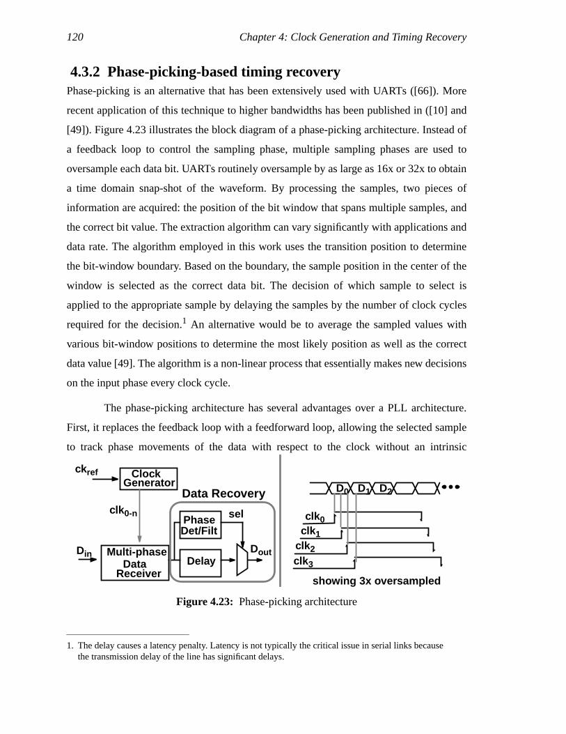
120 Chapter 4: Clock Generation and Timing Recovery
4.3.2 Phase-picking-based timing recoveryPhase-picking is an alternative that has been extensively used with UARTs ([66]). More
recent application of this technique to higher bandwidths has been published in ([10] and
[49]). Figure 4.23 illustrates the block diagram of a phase-picking architecture. Instead of
a feedback loop to control the sampling phase, multiple sampling phases are used to
oversample each data bit. UARTs routinely oversample by as large as 16x or 32x to obtain
a time domain snap-shot of the waveform. By processing the samples, two pieces of
information are acquired: the position of the bit window that spans multiple samples, and
the correct bit value. The extraction algorithm can vary significantly with applications and
data rate. The algorithm employed in this work uses the transition position to determine
the bit-window boundary. Based on the boundary, the sample position in the center of the
window is selected as the correct data bit. The decision of which sample to select is
applied to the appropriate sample by delaying the samples by the number of clock cycles
required for the decision.1 An alternative would be to average the sampled values with
various bit-window positions to determine the most likely position as well as the correct
data value [49]. The algorithm is a non-linear process that essentially makes new decisions
on the input phase every clock cycle.
The phase-picking architecture has several advantages over a PLL architecture.
First, it replaces the feedback loop with a feedforward loop, allowing the selected sample
to track phase movements of the data with respect to the clock without an intrinsic
1. The delay causes a latency penalty. Latency is not typically the critical issue in serial links becausethe transmission delay of the line has significant delays.
Figure 4.23: Phase-picking architecture
PhaseDet/Filt
ClockGenerator
DataReceiver
clk 0-n
Din
ck ref
Multi-phaseDelay
sel
Dout
D0 D1 D2
clk 0clk 1
clk 2clk 3
showing 3x oversampled
Data Recovery
4.3 Timing-Recovery Architectures 121
bandwidth limitation. The maximum tracking rate is limited by the transition information
present. This fast tracking can potentially track the transmit PLL’s jitter accumulation,
which appears as data jitter. Because the sampling clocks are generated by an on-chip
PLL, phase-picking can also track the jitter accumulation from the VCO of the receiver
clock generator.
A second advantage of the phase-picking architecture is that long PLL phase-
locking time is not needed. Phase decisions are made whenever input transitions are
present. The technique is suitable for switched networks ([6], [10], and [24]) where the
timing of the signal must be acquired in the few header bytes of the packet.
Due to the higher tracking bandwidth, a limitation of the technique is that the
system cannot tolerate large cycle-to-cycle1 jitter. Phase changes (φerr) greater than half
the bit-time (π) are indistinguishable from a phase shift in the opposite direction,φerr-2π.
Note that, although the cycle-to-cycle jitter is limited, the peak-to-peak jitter can be much
larger than a bit-time (i.e., peak-to-peak jitter > cycle-to-cycle jitter). For bandwidth
limited systems such as a PLL, average phase is used instead of trying to follow the fast
phase movements. If the phase noise is uncorrelated from one cycle to the next, by
averaging, the peak-to-peak jitter can be as large as the entire timing margin (1 bit-time or
2π) instead of half the bit-time. Therefore, the type of timing recovery to use depends on
the phase-noise characteristics of the system. If phase noise has a large correlated
component, such as from the clock/phase-generation PLL, phase-picking would be useful.
If, on the contrary, the dominant noise is from random digital switching coupling directly
onto the clock buffers without the loop’s accumulation, then a lower bandwidth averaging
could potentially achieve better performance.
The primary disadvantage of the architecture is that there is an inherent static
phase error due to the phase quantization. Higher oversampling ratios and finer phase
quantization reduce the static phase error but add significant complexity to the design.
Furthermore, inherent sampler uncertainty limits the minimum quantization error. Based
1. Cycle-to-cycle usually applies to repetitive clock signals. In this case, since data transitions areencoded, “cycle-to-cycle” applies to phase noise between two transitions.
122 Chapter 4: Clock Generation and Timing Recovery
on Chapter 3, the limit is 1/10 FO-4. More significantly, the increased number of samplers
increases the input capacitance, hence limiting the input bandwidth. For high input
bandwidths, the trade-off favors a low oversampling ratio with the penalty of higher static
phase offsets due to the coarse quantization.
The phase-picking architecture was chosen to explore the usefulness of the higher
phase tracking capability for lower jitter at the price of higher static phase error. In a VLSI
implementation, supply and substrate noise can be significant enough for the peak-to-peak
jitter to occupy a large fraction of the bit-time, especially since a PLL accumulates jitter.
Based on the PLL description of Section 4.1, the peak-to-peak jitter from these clock
generators can be greater than 1/2 bit-time. For the 4-Gb/s test chip with a bit-time of 1
FO-4 (250ps), the 3x oversampled phase-picking scheme can track the noise of the on-
chip multiple clock phase generators (PLLs) from both the transmitter and the receiver to
keep the total effective jitter below the quantization spacing of 1/3 bit-time (83ps).
As does the PLL bandwidth, the maximum phase-picker tracking rate depends on
the data transition density. Typically 8B/10B coding is used. In this design, instead of an
8B/10B code which is more complex to implement, a PRBS encoder with sequence length
of 27-1 is used to simplify the test chip. The coding guarantees a minimum of one
transition per byte which is only slightly worse than the 8B/10B code. For a simple
implementation where the decision logic operates at the rate of the demultiplexed clock,
the tracking rate can be one sample spacing every transition, 1/3 bit-time/cycle (83ps/2ns,
or 4% of the period per clock cycle). The maximum static phase error from the
quantization is 1/6 FO-4 (2% of the clock period). Since the static phase error is
comparable to a PLL’s static phase error, this architecture shows promise of being more
robust to large phase noise.
4.4 Timing-Recovery ImplementationThe principal component in the phase-picking architecture is the decision algorithm. The
decision algorithm processes the oversampled information, decides where the bit
boundaries lie, and chooses which sample to pick. With one transition per 8 bits and 3x
oversampling, the phase picker can track at a rate of 1/3 bit-time/8 bits (83ps/2ns); and the
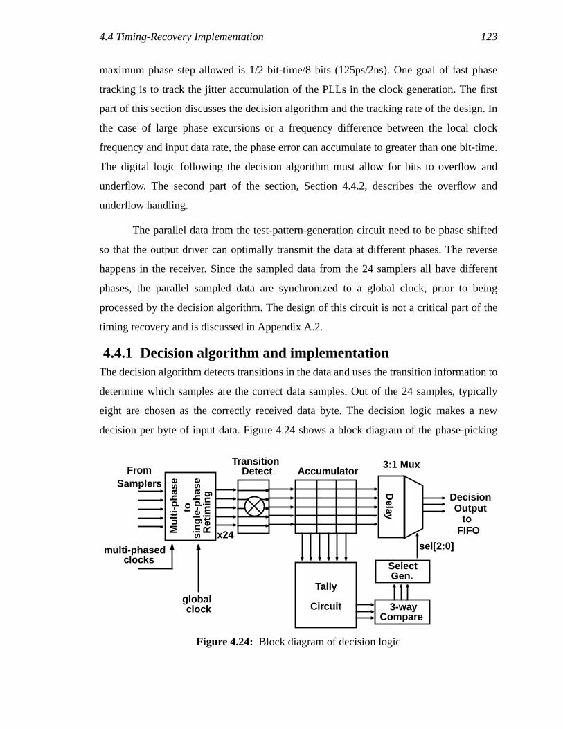
4.4 Timing-Recovery Implementation 123
maximum phase step allowed is 1/2 bit-time/8 bits (125ps/2ns). One goal of fast phase
tracking is to track the jitter accumulation of the PLLs in the clock generation. The first
part of this section discusses the decision algorithm and the tracking rate of the design. In
the case of large phase excursions or a frequency difference between the local clock
frequency and input data rate, the phase error can accumulate to greater than one bit-time.
The digital logic following the decision algorithm must allow for bits to overflow and
underflow. The second part of the section, Section 4.4.2, describes the overflow and
underflow handling.
The parallel data from the test-pattern-generation circuit need to be phase shifted
so that the output driver can optimally transmit the data at different phases. The reverse
happens in the receiver. Since the sampled data from the 24 samplers all have different
phases, the parallel sampled data are synchronized to a global clock, prior to being
processed by the decision algorithm. The design of this circuit is not a critical part of the
timing recovery and is discussed in Appendix A.2.
4.4.1 Decision algorithm and implementationThe decision algorithm detects transitions in the data and uses the transition information to
determine which samples are the correct data samples. Out of the 24 samples, typically
eight are chosen as the correctly received data byte. The decision logic makes a new
decision per byte of input data. Figure 4.24 shows a block diagram of the phase-picking
Figure 4.24: Block diagram of decision logic
x24Ret
imin
g
TransitionAccumulator
3-wayCompare
SelectGen.
3:1 Mux
DecisionOutput
Detect
Mul
ti-ph
ase
tosi
ngle
-pha
se
FromSamplers
toFIFO
multi-phasedclocks
globalclock
Delay
sel[2:0]
Tally
Circuit
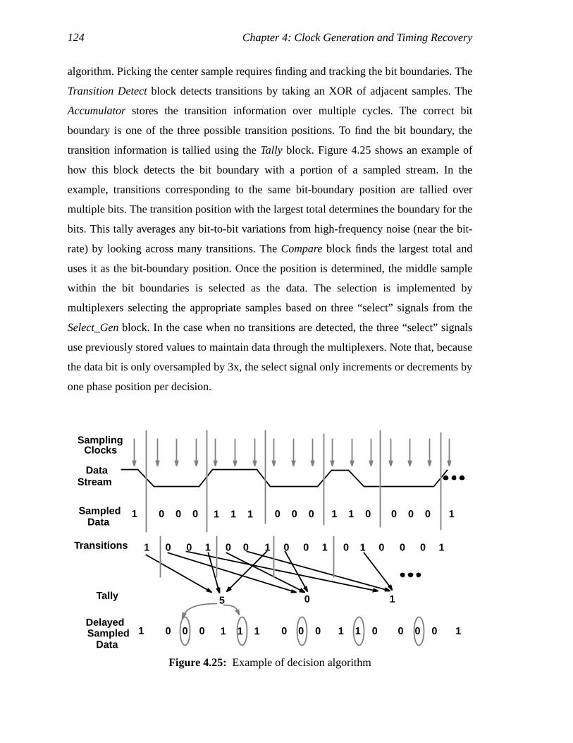
124 Chapter 4: Clock Generation and Timing Recovery
algorithm. Picking the center sample requires finding and tracking the bit boundaries. The
Transition Detect block detects transitions by taking an XOR of adjacent samples. The
Accumulator stores the transition information over multiple cycles. The correct bit
boundary is one of the three possible transition positions. To find the bit boundary, the
transition information is tallied using theTally block. Figure 4.25 shows an example of
how this block detects the bit boundary with a portion of a sampled stream. In the
example, transitions corresponding to the same bit-boundary position are tallied over
multiple bits. The transition position with the largest total determines the boundary for the
bits. This tally averages any bit-to-bit variations from high-frequency noise (near the bit-
rate) by looking across many transitions. TheCompare block finds the largest total and
uses it as the bit-boundary position. Once the position is determined, the middle sample
within the bit boundaries is selected as the data. The selection is implemented by
multiplexers selecting the appropriate samples based on three “select” signals from the
Select_Gen block. In the case when no transitions are detected, the three “select” signals
use previously stored values to maintain data through the multiplexers. Note that, because
the data bit is only oversampled by 3x, the select signal only increments or decrements by
one phase position per decision.
Figure 4.25: Example of decision algorithm
1
1
Sampled
Transitions
5 0 1Tally
SamplingClocks
DataStream
Data
SampledData
Delayed
1 1 1 0 0 0 0 0 0 1 1 0 0 0 0 1
1 1 1 0 10 0 0 0 0 0 0 1 0 0
1 1 1 1 0 0 0 0 0 0 1 1 0 0 0 0 1
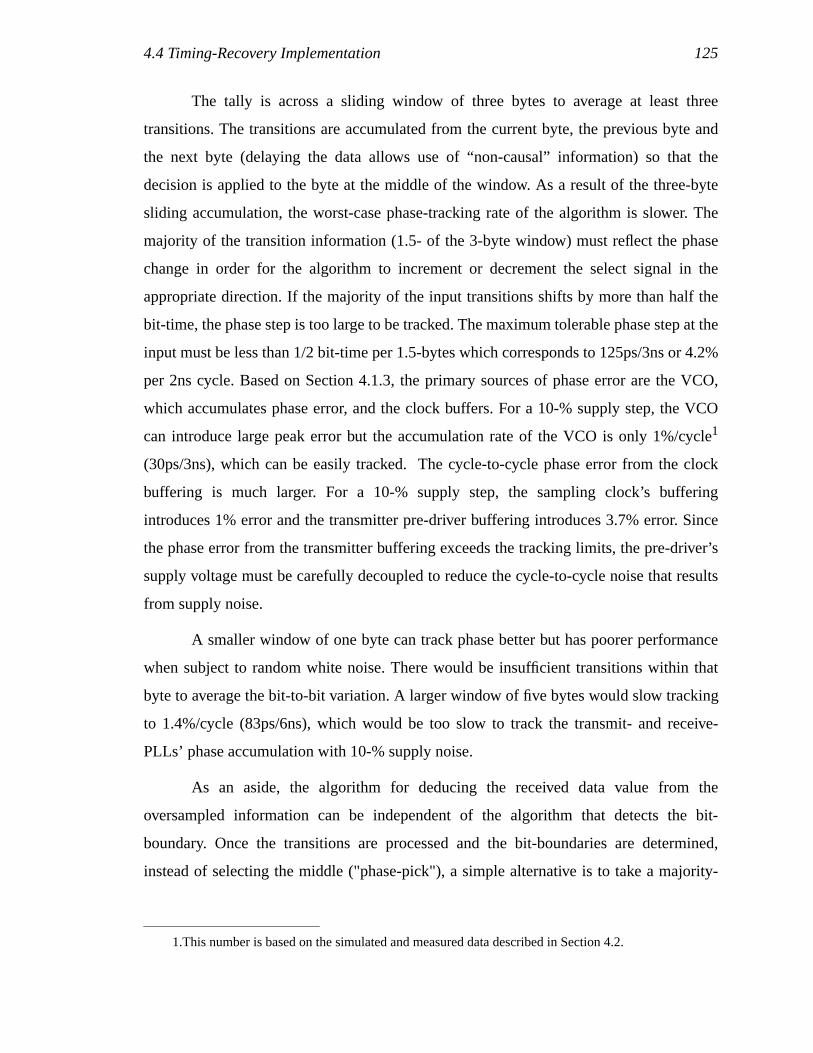
4.4 Timing-Recovery Implementation 125
The tally is across a sliding window of three bytes to average at least three
transitions. The transitions are accumulated from the current byte, the previous byte and
the next byte (delaying the data allows use of “non-causal” information) so that the
decision is applied to the byte at the middle of the window. As a result of the three-byte
sliding accumulation, the worst-case phase-tracking rate of the algorithm is slower. The
majority of the transition information (1.5- of the 3-byte window) must reflect the phase
change in order for the algorithm to increment or decrement the select signal in the
appropriate direction. If the majority of the input transitions shifts by more than half the
bit-time, the phase step is too large to be tracked. The maximum tolerable phase step at the
input must be less than 1/2 bit-time per 1.5-bytes which corresponds to 125ps/3ns or 4.2%
per 2ns cycle. Based on Section 4.1.3, the primary sources of phase error are the VCO,
which accumulates phase error, and the clock buffers. For a 10-% supply step, the VCO
can introduce large peak error but the accumulation rate of the VCO is only 1%/cycle1
(30ps/3ns), which can be easily tracked. The cycle-to-cycle phase error from the clock
buffering is much larger. For a 10-% supply step, the sampling clock’s buffering
introduces 1% error and the transmitter pre-driver buffering introduces 3.7% error. Since
the phase error from the transmitter buffering exceeds the tracking limits, the pre-driver’s
supply voltage must be carefully decoupled to reduce the cycle-to-cycle noise that results
from supply noise.
A smaller window of one byte can track phase better but has poorer performance
when subject to random white noise. There would be insufficient transitions within that
byte to average the bit-to-bit variation. A larger window of five bytes would slow tracking
to 1.4%/cycle (83ps/6ns), which would be too slow to track the transmit- and receive-
PLLs’ phase accumulation with 10-% supply noise.
As an aside, the algorithm for deducing the received data value from the
oversampled information can be independent of the algorithm that detects the bit-
boundary. Once the transitions are processed and the bit-boundaries are determined,
instead of selecting the middle ("phase-pick"), a simple alternative is to take a majority-
1.This number is based on the simulated and measured data described in Section 4.2.
126 Chapter 4: Clock Generation and Timing Recovery
vote based on the three sampled values such as in the design by Kim in [49]. Figure 4.26
shows a simulated performance comparison of its BER vs.SNR. Majority voting works
well with non-bandwidth-limited signals that have high-frequency noise because the
algorithm averages the noise of each sample over all samples in a bit. However, in a
system that is bandwidth-limited by the input and output RC filters, it performs worse
because the non-middle samples have much higher probability of error.
One final detail in the algorithm is the special condition where two transition
positions have equal counts. This occurs when two of the sample positions straddle the
center of the bit and the third sampler samples at the transition. Picking either of the two
straddling the center should give the same performance. In this implementation, the
previous, current and next cycles’ “select” results are used to follow the direction of any
phase transition. However, because the condition is rare, it only yields marginally better
SNRof 1dB in simulation.
The implementation uses a divided-by-two clock (250MHz) for the decision logic
instead of the 500MHz oscillator clock. This allows a relaxed cycle-time of 16 FO-4 to
perform the decision processing so that the clock cycle-time is not constrained by the
Figure 4.26: Comparison of majority voting (unfilled-circle symbols) with center-picking(filled-diamond symbols).
8.0 9.0 10.0 11.0 12.0 13.0 14.0-8.0
-7.0
-6.0
-5.0
-4.0
-3.0
-2.0
-1.0
Majority Voting
Center Picking
S/N (dB)
Sim
ulat
ed P
RB
S 2
7 -1
BE
R (
log)
4.4 Timing-Recovery Implementation 127
complexity of the logic. The tracking rate is not penalized by this demultiplexing because
the decisions for the data are made for each byte of data (2 decisions per clock cycle).1
4.4.2 Handling frequency offsetIf the peak-to-peak phase jitter is larger than one bit-time, or if the transmitter and receiver
operate at different frequencies, the tracking must allow bit(s) to overflow/underflow. For
example, if thesel2:0 signal changes from 0-0-1 to 1-0-0, the selected sample of the first
cycle corresponds to the same bit as the selected sample of the following cycle. This
"underflow" condition must be appropriately handled by dropping one of the two samples.
Typically, these samples are of the same bit and thus have the same value. However, in the
case where they are different, dropping the latter gives a slight performance improvement,
if phase movement changes directions (thesel signal returns to 0-0-1) in the following
cycle’s decision. Similar to the “underflow” where one fewer bit is received, the opposite
transition from 1-0-0 to 0-0-1 causes an “overflow”, requiring an extra bit to be stored.
In the implementation, because of the 1:2 demultiplexing from a 500-MHz sample
clock frequency to a 250-MHz internal clock frequency, the internal logic is simplified by
allowing only one overflow/underflow bit per input word (2-bytes) reducing the maximum
frequency offset that can be handled to 2.1% of the 250-MHz clock (1/3 bit-time per 4ns).
However, the jitter tracking rate is not compromised because the select signals are allowed
to be different for the first byte and second byte of the word. So an “overflow” condition
corresponds to a 17-bit output of the decision logic while an “underflow” corresponds to
15 bits of output.
These extra bits are handled by a bit-wise FIFO that operates as a shifter. Because
the final output handles one word per cycle, the additional bit from an overflow must be
stored and any missing bit from an underflow must be supplied. The shifter feeds into a
bank of registers. By shifting the position in which the word is written into this bank, bits
are not overwritten and no single-bit bubbles are left in the register when there is an
overflow or underflow. In every cycle, a word is taken from the register bank. The register
bank is wide enough to allow an entire word of overflow or underflow. To allow more than
1. So,Select_Gen outputs two sets of select signals every cycle, one for each byte of data.
128 Chapter 4: Clock Generation and Timing Recovery
one word of overflow or underflow, a word-wise FIFO follows the register to supply
additional storage depth. The depth of this FIFO determines the number of overflowing
bits before valid data is dropped. Therefore, the maximum packet length that the
transceiver can handle depends on the frequency difference between the local clock and
the demultiplexed data rate.
If the application requires handling long data streams, instead of constantly
overflowing or underflowing, the local frequency can be corrected based on the phase
information from the decision logic. Because the decision logic can essentially behave as a
phase detector, the select signals can easily be filtered for a low bandwidth control loop to
control the external frequency.1 This correction can also adjust the center sample to be, on
average, at the middle of the bit-window which potentially improves the quantization error
of phase-picking. Because this correction is low bandwidth, the phase-picking could still
be useful in handling large excursions in phase due to large peak-to-peak jitter.
4.5 SummaryThis chapter addressed two issues: generating the multiple clock phases for the transmitter
and receiver, and ensuring a good timing relationship between the input data and sampling
clock. Both affect the timing margin of the system and hence affect the performance.
Accurate clock phases with spacing of 1/3 of a bit-time are generated by tapping
from a VCO and interpolating between the tapped phases. The accuracy of the phase
spacing has been simulated and measured to be roughly 13% of the delay of the VCO
element for the receiver and 7% for the transmitter. This is sufficiently low for the 8:1
multiplexing and 1:8 demultiplexing of the I/O circuits. However, the primary source of
the error is due to device mismatches, which only worsens with better technologies.
Although the errors do not pose any problems for a 0.35-µm process technology, they
become significant with more advanced technologies.
Ensuring a small timing error between the input data and the sampling clocks
depends not only on the jitter of the clock generation circuit but also the timing-recovery
1. This logic was not implemented in the transceiver design.
4.5 Summary 129
circuit. Two types of timing-recovery schemes were discussed. This dissertation chose to
explore the oversampled phase-picking technique because the scheme potentially provides
a higher tracking bandwidth and greater robustness to phase noise. A low degree of
oversampling by 3x is chosen to minimize the overhead of the oversampling and to utilize
the sampler’s ability to sample faster than the bit-rate.
Beside the greater area and power overhead, the primary disadvantage of the
technique is that the phase quantization error appears as a systematic static phase offset.
With 3x oversampling, the error is 1/6 bit-time. The advantage is that the phase-picking
logic adjusts the sample that is selected every 500-MHz clock cycle (every byte of data).
This fast correction potentially restricts the maximum error to 1/6 bit-time as long as the
input phase steps do not exceed 4.2%/cycle. Whether this constraint is met depends on the
noise conditions of the actual system. The tracking rate can tolerate greater than 10-%
supply noise at the oscillator and receiver and 5-% supply noise at the transmitter.

130 Chapter 4: Clock Generation and Timing Recovery
131
Chapter 5
Experimental Results
A transceiver test-chip using the transmitter, receiver, and timing-recovery designs
described in the previous chapters was implemented in a 0.5-µm process technology from
HP (MOSIS) and a 0.35-µm process technology from LSI. The FO-4 delay of the two
processes are 240ps and 170ps, corresponding to 4Gb/s and 6Gb/s, respectively, for a
target bit-time of 1 FO-4.
The bandwidth of the link and the noise in the system depend on the design of the
channel. To be able to measure the technology limitations, the channel needs to be as ideal
as possible. Section 5.1 describes the connection between the transmitter and receiver used
in the test setup and presents issues with the board design and the chip packaging. Section
5.2 describes the transceiver test chip in more detail, explaining the test circuitry. The
following two sections, Section 5.3 and Section 5.4, discuss the experimental results from
independent measurements of the transmitter and receiver. Finally, to verify the
performance of the transceiver, bit-error-rate measurements are discussed in Section 5.5.
The overall performance is demonstrated with BER versusSNR plots under different noise
and input conditions. Furthermore, to demonstrate the robustness to noise of the phase-
picking data-recovery scheme, transceiver performance is measured with induced phase
noise.
132 Chapter 5: Experimental Results
5.1 ChannelThe channel can limit performance by both limiting the signalling bandwidth and
introducing noise in the signal. For the transceiver tests, the transmitted signal travels
through the transmitter chip carrier (package), a segment of printed-circuit board (PCB)
trace, a coaxial cable, back through a PCB trace, and then the receiver chip carrier. The
channel is terminated at the end with a resistor.
The first part of this section describes the coaxial cable and PCB trace used in the
test setup, while the rest of the section examines the chip-packaging issues. In particular,
package inductance is directly in the signal path which both low-pass filters the signal and
couples the signal with other signals, introducing crosstalk. To measure the characteristics
of the complete channel and to model the channel in simulation, a time-domain
reflectometry (TDR) measurement is taken and described in the final part of this section.
5.1.1 Cable and PCBTo maintain high bandwidths, very high-quality cables and board materials are used for
the experiments. Although rigid coaxial cables are the highest quality, with loss less than
0.1dB/m at 4GHz [18], their rigid casing makes multiple test configurations inconvenient.
Instead, conformable cables1 are used, which have their braided shield dipped in soft
solder. The non-porous shield can reduce loss at high frequencies to less than 0.3dB/m at
4GHz.
An SMA connector and cable provides the connection between the board and the
test equipment. The design of the SMA launch is shown in Figure 5.1-(a). The internal
planes are cleared near the center conductor because the connector post capacitively
couples to these planes causing imperfection in the characteristic impedance.
The board material is also selected so as to not introduce additional loss. For
frequencies as high as several gigahertz, the typical board material, FR-4, contributes
roughly 0.03 dB/cm/GHz of signal loss. An additional concern of FR-4 is that the medium
is not uniform. The fibers within the material have directionality, causing mismatches
1. Supplied by First Source Inc.
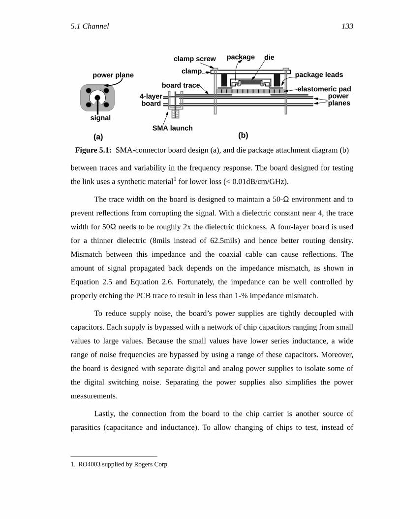
5.1 Channel 133
between traces and variability in the frequency response. The board designed for testing
the link uses a synthetic material1 for lower loss (< 0.01dB/cm/GHz).
The trace width on the board is designed to maintain a 50-Ω environment and to
prevent reflections from corrupting the signal. With a dielectric constant near 4, the trace
width for 50Ω needs to be roughly 2x the dielectric thickness. A four-layer board is used
for a thinner dielectric (8mils instead of 62.5mils) and hence better routing density.
Mismatch between this impedance and the coaxial cable can cause reflections. The
amount of signal propagated back depends on the impedance mismatch, as shown in
Equation 2.5 and Equation 2.6. Fortunately, the impedance can be well controlled by
properly etching the PCB trace to result in less than 1-% impedance mismatch.
To reduce supply noise, the board’s power supplies are tightly decoupled with
capacitors. Each supply is bypassed with a network of chip capacitors ranging from small
values to large values. Because the small values have lower series inductance, a wide
range of noise frequencies are bypassed by using a range of these capacitors. Moreover,
the board is designed with separate digital and analog power supplies to isolate some of
the digital switching noise. Separating the power supplies also simplifies the power
measurements.
Lastly, the connection from the board to the chip carrier is another source of
parasitics (capacitance and inductance). To allow changing of chips to test, instead of
1. RO4003 supplied by Rogers Corp.
Figure 5.1: SMA-connector board design (a), and die package attachment diagram (b)
4-layerboard
clamp screw
SMA launch
package die
clamp package leads
board trace
powerplanes
elastomeric pad
power plane
signal
(b)(a)
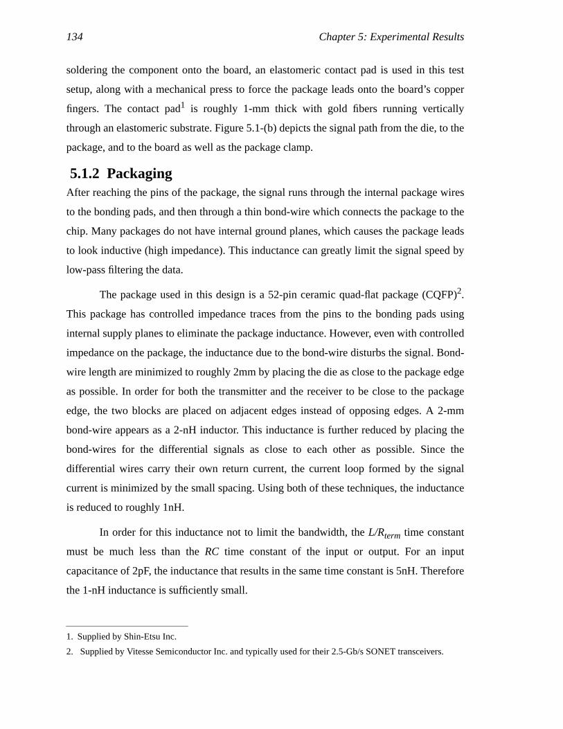
134 Chapter 5: Experimental Results
soldering the component onto the board, an elastomeric contact pad is used in this test
setup, along with a mechanical press to force the package leads onto the board’s copper
fingers. The contact pad1 is roughly 1-mm thick with gold fibers running vertically
through an elastomeric substrate. Figure 5.1-(b) depicts the signal path from the die, to the
package, and to the board as well as the package clamp.
5.1.2 PackagingAfter reaching the pins of the package, the signal runs through the internal package wires
to the bonding pads, and then through a thin bond-wire which connects the package to the
chip. Many packages do not have internal ground planes, which causes the package leads
to look inductive (high impedance). This inductance can greatly limit the signal speed by
low-pass filtering the data.
The package used in this design is a 52-pin ceramic quad-flat package (CQFP)2.
This package has controlled impedance traces from the pins to the bonding pads using
internal supply planes to eliminate the package inductance. However, even with controlled
impedance on the package, the inductance due to the bond-wire disturbs the signal. Bond-
wire length are minimized to roughly 2mm by placing the die as close to the package edge
as possible. In order for both the transmitter and the receiver to be close to the package
edge, the two blocks are placed on adjacent edges instead of opposing edges. A 2-mm
bond-wire appears as a 2-nH inductor. This inductance is further reduced by placing the
bond-wires for the differential signals as close to each other as possible. Since the
differential wires carry their own return current, the current loop formed by the signal
current is minimized by the small spacing. Using both of these techniques, the inductance
is reduced to roughly 1nH.
In order for this inductance not to limit the bandwidth, theL/Rterm time constant
must be much less than theRC time constant of the input or output. For an input
capacitance of 2pF, the inductance that results in the same time constant is 5nH. Therefore
the 1-nH inductance is sufficiently small.
1. Supplied by Shin-Etsu Inc.
2. Supplied by Vitesse Semiconductor Inc. and typically used for their 2.5-Gb/s SONET transceivers.
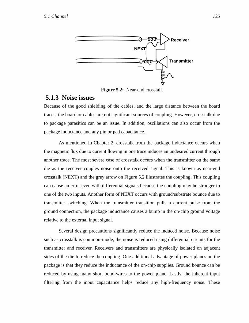
5.1 Channel 135
5.1.3 Noise issuesBecause of the good shielding of the cables, and the large distance between the board
traces, the board or cables are not significant sources of coupling. However, crosstalk due
to package parasitics can be an issue. In addition, oscillations can also occur from the
package inductance and any pin or pad capacitance.
As mentioned in Chapter 2, crosstalk from the package inductance occurs when
the magnetic flux due to current flowing in one trace induces an undesired current through
another trace. The most severe case of crosstalk occurs when the transmitter on the same
die as the receiver couples noise onto the received signal. This is known as near-end
crosstalk (NEXT) and the grey arrow on Figure 5.2 illustrates the coupling. This coupling
can cause an error even with differential signals because the coupling may be stronger to
one of the two inputs. Another form of NEXT occurs with ground/substrate bounce due to
transmitter switching. When the transmitter transition pulls a current pulse from the
ground connection, the package inductance causes a bump in the on-chip ground voltage
relative to the external input signal.
Several design precautions significantly reduce the induced noise. Because noise
such as crosstalk is common-mode, the noise is reduced using differential circuits for the
transmitter and receiver. Receivers and transmitters are physically isolated on adjacent
sides of the die to reduce the coupling. One additional advantage of power planes on the
package is that they reduce the inductance of the on-chip supplies. Ground bounce can be
reduced by using many short bond-wires to the power plane. Lastly, the inherent input
filtering from the input capacitance helps reduce any high-frequency noise. These
Figure 5.2: Near-end crosstalk
NEXT
Transmitter
Receiver
136 Chapter 5: Experimental Results
techniques were very successful in reducing the noise in the experimental prototype. The
receiver was tested with and without the transmitter operating, without any noticeable
performance difference.
One other significant effect of the inductance is that it forms a tuned circuit with
the pin and pad capacitance, which causes ringing. If this ringing occurs at a frequency
near the signalling rate, it interferes with the signal being transmitted or received. The
ringing frequency for the 1-nH bond-wire and 2-pF capacitor is roughly 4GHz (two times
the targeted data rate). Whether the termination resistor is placed on-chip or off-chip
therefore can have a significant impact. Because the resistance is low, an on-chip resistor
would dampen the ringing. Figure 5.3-(b) illustrates the damped response with the 50-Ω
termination resistor. This damping is especially significant for the transmitter, because the
large current switched by one branch of the transmitter exhibits an overshoot which then
interferes with subsequent transmitted signals by other branches. Since the driver is a
current source, the damping is insufficient without the resistor, as demonstrated in the
peak in the simulation of Figure 5.3-(a). The overshoot is observed at the output of the
Figure 5.3: On-chip termination for current-mode driver and simulation results. (a)shows off-chip termination (grey line), and (b) shows on-chip termination (black line).
2.0 2.1 2.20.85
0.90
0.95
1.00
on-chip terminationoff-chip termination
2.3time (ns)
Out
put V
olta
ge (
%V
dd)
50ΩTransmission
Line
package
Lbond
Rterm
Cpad
50ΩTransmission
Line
package
Lbond
Rterm
Cpad
(a)
(b)
(a)
(b)
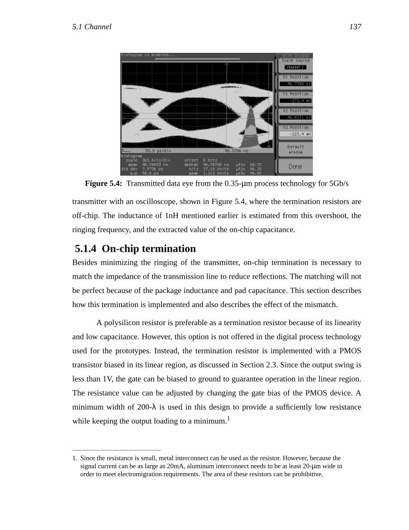
5.1 Channel 137
transmitter with an oscilloscope, shown in Figure 5.4, where the termination resistors are
off-chip. The inductance of 1nH mentioned earlier is estimated from this overshoot, the
ringing frequency, and the extracted value of the on-chip capacitance.
5.1.4 On-chip terminationBesides minimizing the ringing of the transmitter, on-chip termination is necessary to
match the impedance of the transmission line to reduce reflections. The matching will not
be perfect because of the package inductance and pad capacitance. This section describes
how this termination is implemented and also describes the effect of the mismatch.
A polysilicon resistor is preferable as a termination resistor because of its linearity
and low capacitance. However, this option is not offered in the digital process technology
used for the prototypes. Instead, the termination resistor is implemented with a PMOS
transistor biased in its linear region, as discussed in Section 2.3. Since the output swing is
less than 1V, the gate can be biased to ground to guarantee operation in the linear region.
The resistance value can be adjusted by changing the gate bias of the PMOS device. A
minimum width of 200-λ is used in this design to provide a sufficiently low resistance
while keeping the output loading to a minimum.1
1. Since the resistance is small, metal interconnect can be used as the resistor. However, because thesignal current can be as large as 20mA, aluminum interconnect needs to be at least 20-µm wide inorder to meet electromigration requirements. The area of these resistors can be prohibitive.
Figure 5.4: Transmitted data eye from the 0.35-µm process technology for 5Gb/s
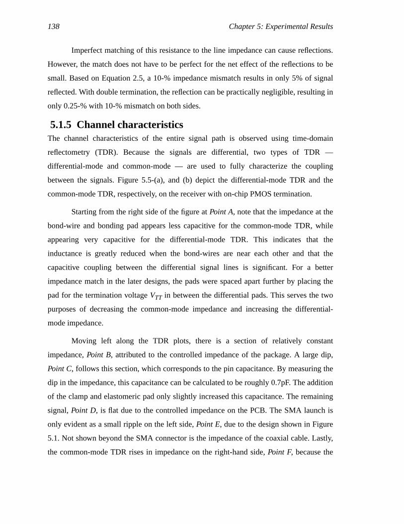
138 Chapter 5: Experimental Results
Imperfect matching of this resistance to the line impedance can cause reflections.
However, the match does not have to be perfect for the net effect of the reflections to be
small. Based on Equation 2.5, a 10-% impedance mismatch results in only 5% of signal
reflected. With double termination, the reflection can be practically negligible, resulting in
only 0.25-% with 10-% mismatch on both sides.
5.1.5 Channel characteristicsThe channel characteristics of the entire signal path is observed using time-domain
reflectometry (TDR). Because the signals are differential, two types of TDR —
differential-mode and common-mode — are used to fully characterize the coupling
between the signals. Figure 5.5-(a), and (b) depict the differential-mode TDR and the
common-mode TDR, respectively, on the receiver with on-chip PMOS termination.
Starting from the right side of the figure atPoint A, note that the impedance at the
bond-wire and bonding pad appears less capacitive for the common-mode TDR, while
appearing very capacitive for the differential-mode TDR. This indicates that the
inductance is greatly reduced when the bond-wires are near each other and that the
capacitive coupling between the differential signal lines is significant. For a better
impedance match in the later designs, the pads were spaced apart further by placing the
pad for the termination voltageVTT in between the differential pads. This serves the two
purposes of decreasing the common-mode impedance and increasing the differential-
mode impedance.
Moving left along the TDR plots, there is a section of relatively constant
impedance,Point B, attributed to the controlled impedance of the package. A large dip,
Point C, follows this section, which corresponds to the pin capacitance. By measuring the
dip in the impedance, this capacitance can be calculated to be roughly 0.7pF. The addition
of the clamp and elastomeric pad only slightly increased this capacitance. The remaining
signal,Point D, is flat due to the controlled impedance on the PCB. The SMA launch is
only evident as a small ripple on the left side,Point E, due to the design shown in Figure
5.1. Not shown beyond the SMA connector is the impedance of the coaxial cable. Lastly,
the common-mode TDR rises in impedance on the right-hand side,Point F, because the
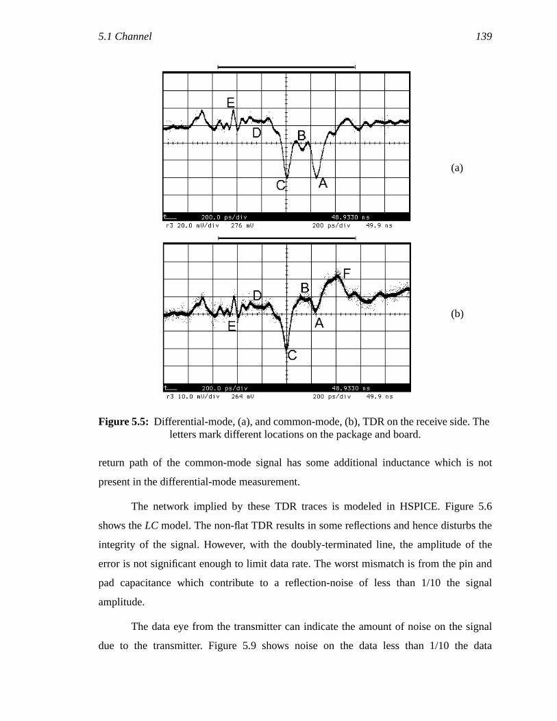
5.1 Channel 139
return path of the common-mode signal has some additional inductance which is not
present in the differential-mode measurement.
The network implied by these TDR traces is modeled in HSPICE. Figure 5.6
shows theLC model. The non-flat TDR results in some reflections and hence disturbs the
integrity of the signal. However, with the doubly-terminated line, the amplitude of the
error is not significant enough to limit data rate. The worst mismatch is from the pin and
pad capacitance which contribute to a reflection-noise of less than 1/10 the signal
amplitude.
The data eye from the transmitter can indicate the amount of noise on the signal
due to the transmitter. Figure 5.9 shows noise on the data less than 1/10 the data
Figure 5.5: Differential-mode, (a), and common-mode, (b), TDR on the receive side. Theletters mark different locations on the package and board.
(a)
(b)
140 Chapter 5: Experimental Results
amplitude. The noise in Figure 5.4 is higher because of the noise from the ringing and
phase noise.
5.2 Transceiver Test ChipThe parallelized transmitter and receiver of Chapter 3 and the oversampled timing-
recovery scheme of Chapter 4 were implemented on a single die. The functional block
diagram of the transceiver test chip is illustrated in Figure 5.7. The chip (including the
bonding pads) occupies 8600 x 8600λ or 3x3mm2 in 0.5-µm technology. Figure 5.8
depicts the chip micrograph with the major functional blocks outlined. This section briefly
describes the different possible test configurations of the chip along with the operation of
blocks that were not discussed in the prior chapters.
The transmitter (left-hand side of the diagram) selects data from three different
sources. The transmitter can be configured to transmit a sequence from the receiver, a
fixed data pattern, or a pseudo-random bit sequence (PRBS) generated locally. The first
configuration allows the chip to operate in a transceive mode. The second configuration
can verify the functionality of the transmitter by fixing the output to a user programmable
16-bit sequence. The final configuration provides for self-testing by transmitting a bit
sequence that can be verified. Prior to transmitting, the parallel data is adjusted in timing
through a synchronization block. This block provides the pre-driver of each of the eight
driver legs with data that is stable while the leg is driving the output current pulse.
Figure 5.6: Board and package electrical model
LC segments
boardtrace
SMAcable SMA connector
couplingL & C
packagetrace
bondwire
50Ω substrateresistance
padcapacitance
5.2 Transceiver Test Chip 141
Because the data from the 24 samplers all have individual phases, the received data
is also synchronized after the oversampling and demultiplexing, synchronizing the
multiple phases to the same timing. Both synchronization circuits are described more fully
in Appendix A.2. The phase-picking logic processes the samples to yield the predicted
data sequence. The sequence can be driven to three different destinations: the high-speed
transmitter to be re-transmitted, the parallel-data drivers to be driven at lower data-rate for
verification, or the PRBS decoder to validate the pseudo-random sequence.
The power dissipation and the area of each of the blocks are listed in Appendix
A.3. Note in Figure 5.8 that the decision algorithm occupies a significant area of 4500λ x
3500λ. This large area is necessary to process the wide data path from the oversampling.
A BER measurement using the PRBS encoder and decoder tests the performance
of the link. An error flag is asserted when the decoder detects an error. The BER can be
determined by counting the number of errors or waiting for the first error to occur. A
PRBS is used to test the BER because it approximates a realistic data sequence and can be
generated from a simple linear-feedback shift-register. Although the sequence is cyclical,
the power spectral density between the repetition frequency and the data frequency is flat.
Figure 5.7: Transceiver chip’s block diagram
TRANSMIT SIDE RECEIVE SIDE
Xcv
Dat
a
Fix
ed D
ata
PRBS Data
Single- φ to Multi- φ Multi- φ to Single- φ
Byte FIFO
PRBS
PRBS
Delay Decision
1:8 Demux Samplers (24)
Data Out @ 4Gbps Data In @ 4Gbps
Ana
log
Rx-
PLL
Ana
log
Tx-
PLL 8:1 Multiplexing Driver
Logic
Bit ShifterEncode
Decode
Select Muxsel
Reg
iste
r
Re-Synchronization Re-Synchronization
Err_Flag
Phase-picking Logic
8 24
8
8
8
3
24 phases
142 Chapter 5: Experimental Results
Since coding typically eliminates the lower frequencies, the PRBS covers all the different
data combinations and represents a realistic data sequence.
The sequence length is chosen to be 27-1 (127), which has a maximum run-length
— consecutive bits of the same value — longer than the 8B/10B DC-balanced code.
Because the on-chip clock rate is 1/8 the data rate, the design is parallelized ([38] and
[59]), in order for the transmitted sequence to be PRBS. Greater details of the design of
the PRBS encoder and decoder is discussed in Appendix A.4. The sequence is also chosen
so that the same sequence can be detected by a BER tester such as the HP-71612A. When
there is a frequency difference between the received data and oversampling clock,
consecutive overflows or underflows can occur, eventually exceeding the depth of the
internal FIFO. In order to test BER over a long measurement period, the PRBS flag is
designed to skip the invalid word or excess word whenever the logic overflows or
underflows by one word.
All these different configurations were implemented so that a fixed pattern can be
used to test the transmitter and receiver individually, and a random pattern can be used to
Figure 5.8: Transceiver chip micrograph
5.3 Transmitter Experimental Results 143
measure the performance of the overall link. The measurement results are discussed in the
following sections.
5.3 Transmitter Experimental ResultsThe functionality and performance of the transmitter is verified by measuring the eye-
opening in the output data. When transmitting the pseudo-random pattern, the output data
appears as a data eye. Since the data stream is formed by a parallelized transmitter that
interleaves eight drivers, a properly measured data eye will show the errors due to
imperfect clock phase spacing and clock jitter. This section describes the measurement
technique and results
As mentioned in Section 4.2, because of the multiple clock phases used for the
multiplexing, the oscilloscope would display a repeating pattern of eight data eyes if it is
triggered with the divide-by-eight frequency. The actual data eye can only be observed
using a trigger frequency at the data rate which would overlay the eight data eyes into a
single eye. The measured data eye is shown in Figure 5.9 from the 0.5-µm process
operating at 3Gb/s. This measurement by a high-speed digital oscilloscope is not at the
nominal operating frequency because the trigger frequency of the oscilloscope is limited
to 3GHz.
Figure 5.9: Measured data eye from the transmitter implemented in the 0.5-µm process
144 Chapter 5: Experimental Results
The reduction in the eye-width is the cumulative effect of the static phase spacing
error as well as jitter. The noise in eye-height is, as mentioned earlier, due to termination
mismatch, package related ringing, switching noise, and supply noise. The bit-width is
degraded by a total of 25%, of which 10% is due to the static phase spacing errors and
15% is due to jitter. The maximum data rate achieved with the transmitter was 4.8Gb/s
before the data eye was degraded by more than 50% (corresponding to 0.83 FO-4). This
result is slightly worse than the simulation results in Section 3.1. The difference can be
accounted for by the 4-stage ring oscillator used to generate the multiple clock phases. As
the frequency is increased, the devices in the VCO leave saturation, and the jitter of the
output data and the sampling clocks increases. Thus, in addition to the closing the data eye
due to the bandwidth limitations, the jitter closes the data eye as well. Similarly, the
maximum data rate of the transmitter built in the 0.35-µm process technology is 6Gb/s1, as
shown in Figure 5.10 with eye-closure of 68ps.
Note that the data eye only demonstrates the functionality of the transmitter. The
actual timing margin of the system is not the size of the data eye because some of the jitter
1. Because of a logic bug found in the 0.5-µm chip, the design was primarily a migration to correct theerror.
Figure 5.10: Measured data eye for 0.35-µm chip operating at 6Gb/s
5.4 Receiver Experimental Results 145
can potentially be tracked by the timing-recovery scheme at the receiver. The functionality
of the full transceiver is addressed in Section 5.5.
5.4 Receiver Experimental ResultsThe two factors that limit the performance of the receiver, as discussed in Section 3.2, are
the input bandwidth (aperture) and the aperture uncertainty. This section describes the
measurements of these two factors to characterize the receiver.
There are several ways to measure the input bandwidth of the receiver. One way is
to send input pulses of diminishing width until the pulse can no longer be resolved. The
minimum resolvable pulse width indicates the maximum input data bit-width. However,
this measurement is difficult because it is hard to generate a very small pulse. Another
method is to use a single-ended input and a varying reference. This method has the
advantage that the input pulse no longer needs to be extremely small. By varying the
reference voltage, the sampling moment changes. The change in sampling moment can be
used to estimate the input slew rate and hence the input time constant. This second method
was used to find that the input time constants of the test chips in the 0.8-µm process and
0.5-µm process are roughly 150ps and 110ps, respectively, which is sufficient for the
bandwidth of 2.5Gb/s and 4.0Gb/s. These measurements of the input bandwidth can not
distinguish between the sampling aperture and the input time constant because only the
overall bandwidth can be measured. These time constants are 1.5x larger than the
simulated value using extracted capacitance. The reason is believed to be due to the pin
capacitance and bond-wire inductance in the signal path which further filter the signal.
The aperture can not be measured directly because it is masked by the input time constant.
The second measurement is of the uncertainty window. The window width
depends primarily on the jitter of the sampling clock and the input-offset voltage of the
comparator.
The receiver clock jitter can be measured by sweeping the timing of a low-jitter,
rising transition at the input with respect to the clock edge with the timing-recovery circuit
disabled. Near the sampling point, theHIGH value is sampled only part of the time due to
the clock jitter. The window in time of the sweep that this uncertainty lasts is the clock
146 Chapter 5: Experimental Results
jitter. The receiver in the 0.5-µm process technology has a measured sampling clock jitter
of roughly 45ps. As in the transmitter, this jitter does not indicate the actual degradation of
the timing margin because the timing-recovery circuit will track out some of the noise.
The second part of the uncertainty window is the data-dependent uncertainty from
the comparator input-offset voltages and sampling-switch non-linearity. This uncertainty
can be measured by performing the static phase spacing measurement with both falling
and rising edge of the input. Any offset of the overlay of these two measurements indicates
the uncertainty. Figure 5.11-(a) illustrates the sampling position spacing (DNL, similar to
Figure 4.21) for both a rising and a falling edge swept across all the samplers for the test-
chip in the 0.35-µm process1. The diamond curve indicates the average of the two. The
sample position of each clock phase is estimated at the center of the jitter uncertainty. The
1. The design in the 0.5-µm process does not allow observability of individual sampler outputs.
Figure 5.11: Measured receiver offset demonstrated by the phase spacing DNL. Theaverage of the input offset for each device, not shown, is less than 1mV.
0.0 4.0 8.0 12.0 16.0 20.0-40.0
-20.0
0.0
20.0
40.0
60.0-20
-10
0.0
10
20
input riseinput fallaverage
erro
r (%
of
inpu
t-of
fset
(m
V)
phase spacing #
ring-
elem
ent d
elay
)
5.5 Transceiver Experimental Results 147
difference in the sample spacing for each position indicates the change in offset from one
sampler to the next. The worst-case error between the two measurements is +/- 6% of the
bit-time (corresponding to 15ps).
The input-referred offset voltage of each sampler can be calculated from Figure
5.11-(a) if the signal slew-rate and the time relationship between the rising and falling
edges are known. However, it is easier to perform a direct measurement using DC voltages
at the input samplers. By varying the input voltage difference, the input-referred offset
voltage can be found by noting voltage that flips the output of the sampler. Figure 5.11-(b)
shows the measured offset for each of the 24 samplers. Because it is difficult to generate
these dc voltages cleanly and accurately, the uncertainty of this measurement is +/- 13mV.
Furthermore, any high-frequency sources of offset are not measured. The peak-to-peak
offset is roughly 100mV for the 0.35-µm process technology. The predicted value from
Section 3.2 is 60mV in the 0.5-µm process and 80mV in the 0.35-µm process.
5.5 Transceiver Experimental ResultsThe final test is to verify the combined operation of the transmitter and the receiver as well
as the timing-recovery scheme. The bit-error rate can be measured as a function ofSNR to
quantify the performance in an actual application. Furthermore, because of the
oversampling, the phase-quantization penalty can be measured. These measurements and
the method used to make these measurements are discussed in the first part of this section.
The second part focuses on the performance of the timing-recovery scheme.
5.5.1 Bit-error-rate measurementsThe BER testing is performed with two different configurations. For the first
measurement, the transmitted output is fed directly back into the input. This tests a
random sequence by using the internal PRBS encoder and decoder. The test yields a BER
of less than 10-14 at a data rate of 1 FO-4. The maximum data rate that can be received
while maintaining a BER of less than 10-9 is 4.3Gb/s. In the 0.35-µm process technology,
the maximum receivable rate is 5.6Gb/s. For both of these chips, the maximum data rate is
limited by a combination of the input time constant and the maximum frequency of the
receiver VCO.
148 Chapter 5: Experimental Results
The second test is configured by placing the chip in a mock optical network as
illustrated in Figure 5.12. A bit-error-rate tester (BERT) is used to generate the data
pattern. The pattern is modulated onto a fiber-optic network. The optical power is
measured by siphoning 1/10 of the total optical power. The optical signal is received and
amplified by an avalanche photodiode (APD), followed by an amplifier. The output of the
amplifier is either returned to the BERT for the baseline measurement, or connected to the
chip configured in its transceiver mode. Because the BERT and optical amplifiers have a
bandwidth limitation of 3-Gb/s, the experimental results of this configuration are limited
in data rate. As mentioned in Section 4.2, the phase spacing at lower frequencies is worse
so the performance can be expected to be slightly worse than when operating at 4.0Gb/s.
The BER versusSNR for the 0.5-µm transceiver chip is plotted in Figure 5.13 withSNR
expressed in optical power. The figure illustrates both the baseline measurement and the
measurement with the DUT. TheSNRpenalty for inserting the DUT to receive and then
re-transmit the data is 1.5dB at 10-9 BER.
An interesting observation is that the measured BER with the DUT does not fall as
quickly at higher signal power. Three reasons account for this. First, the BER tester
receives the transmitted signal using an extremely clean clock position statically at the
center of the bit. No tracking of the transmitter phase noise occurs, hence the phase noise
(especially due to slow frequency temperature drifts) degrades the performance.
Measurements with the transmitter alone yields a BER floor of roughly 10-12 to 10-13
depending on the room conditions. A second cause is the AWGN amplitude noise
introduced in the prior experiment. As discussed in Section 2.2, the amplitude noise can
Figure 5.12: BER measure test setup
BERT3Gb/sPRBS
Dout
OpticalChannel
Modulator
OpticalPowerMeter
PIN
Limiting
Din
XCVR BERT3Gb/sPRBS
Baseline
Amplifier
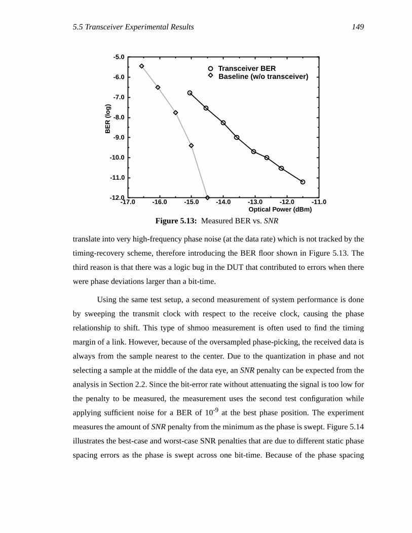
5.5 Transceiver Experimental Results 149
translate into very high-frequency phase noise (at the data rate) which is not tracked by the
timing-recovery scheme, therefore introducing the BER floor shown in Figure 5.13. The
third reason is that there was a logic bug in the DUT that contributed to errors when there
were phase deviations larger than a bit-time.
Using the same test setup, a second measurement of system performance is done
by sweeping the transmit clock with respect to the receive clock, causing the phase
relationship to shift. This type of shmoo measurement is often used to find the timing
margin of a link. However, because of the oversampled phase-picking, the received data is
always from the sample nearest to the center. Due to the quantization in phase and not
selecting a sample at the middle of the data eye, anSNR penalty can be expected from the
analysis in Section 2.2. Since the bit-error rate without attenuating the signal is too low for
the penalty to be measured, the measurement uses the second test configuration while
applying sufficient noise for a BER of 10-9 at the best phase position. The experiment
measures the amount ofSNR penalty from the minimum as the phase is swept. Figure 5.14
illustrates the best-case and worst-case SNR penalties that are due to different static phase
spacing errors as the phase is swept across one bit-time. Because of the phase spacing
Figure 5.13: Measured BER vs.SNR
-17.0 -16.0 -15.0 -14.0 -13.0 -12.0 -11.0-12.0
-11.0
-10.0
-9.0
-8.0
-7.0
-6.0
-5.0
Transceiver BERBaseline (w/o transceiver)
Optical Power (dBm)
BE
R (
log)
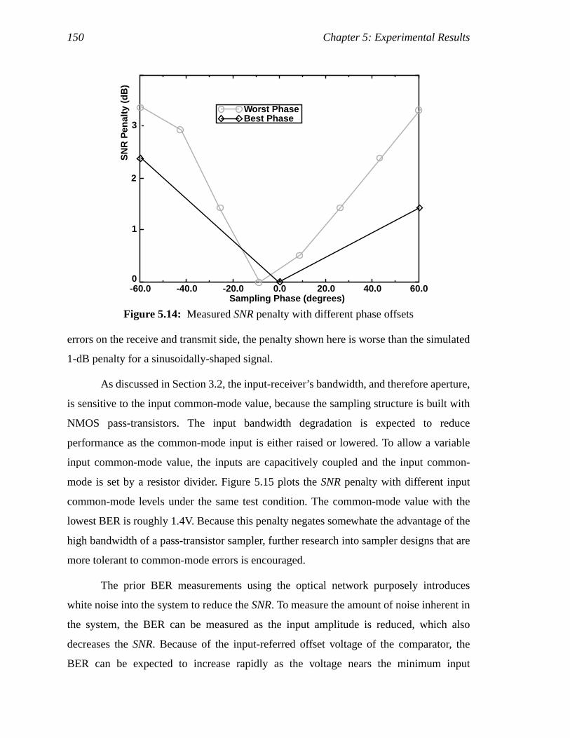
150 Chapter 5: Experimental Results
errors on the receive and transmit side, the penalty shown here is worse than the simulated
1-dB penalty for a sinusoidally-shaped signal.
As discussed in Section 3.2, the input-receiver’s bandwidth, and therefore aperture,
is sensitive to the input common-mode value, because the sampling structure is built with
NMOS pass-transistors. The input bandwidth degradation is expected to reduce
performance as the common-mode input is either raised or lowered. To allow a variable
input common-mode value, the inputs are capacitively coupled and the input common-
mode is set by a resistor divider. Figure 5.15 plots theSNR penalty with different input
common-mode levels under the same test condition. The common-mode value with the
lowest BER is roughly 1.4V. Because this penalty negates somewhate the advantage of the
high bandwidth of a pass-transistor sampler, further research into sampler designs that are
more tolerant to common-mode errors is encouraged.
The prior BER measurements using the optical network purposely introduces
white noise into the system to reduce theSNR. To measure the amount of noise inherent in
the system, the BER can be measured as the input amplitude is reduced, which also
decreases theSNR. Because of the input-referred offset voltage of the comparator, the
BER can be expected to increase rapidly as the voltage nears the minimum input
Figure 5.14: MeasuredSNR penalty with different phase offsets
-60.0 -40.0 -20.0 0.0 20.0 40.0 60.0
Worst PhaseBest Phase
SN
R P
enal
ty (
dB)
Sampling Phase (degrees)
0
3
2
1
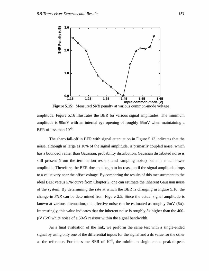
5.5 Transceiver Experimental Results 151
amplitude. Figure 5.16 illustrates the BER for various signal amplitudes. The minimum
amplitude is 90mV with an internal eye opening of roughly 65mV when maintaining a
BER of less than 10-9.
The sharp fall-off in BER with signal attenuation in Figure 5.13 indicates that the
noise, although as large as 10% of the signal amplitude, is primarily coupled noise, which
has a bounded, rather than Gaussian, probability distribution. Gaussian distributed noise is
still present (from the termination resistor and sampling noise) but at a much lower
amplitude. Therefore, the BER does not begin to increase until the signal amplitude drops
to a value very near the offset voltage. By comparing the results of this measurement to the
ideal BER versus SNR curve from Chapter 2, one can estimate the inherent Gaussian noise
of the system. By determining the rate at which the BER is changing in Figure 5.16, the
change inSNR can be determined from Figure 2.5. Since the actual signal amplitude is
known at various attenuation, the effective noise can be estimated as roughly 2mV (6σ).
Interestingly, this value indicates that the inherent noise is roughly 5x higher than the 400-
µV (6σ) white noise of a 50-Ω resistor within the signal bandwidth.
As a final evaluation of the link, we perform the same test with a single-ended
signal by using only one of the differential inputs for the signal and a dc value for the other
as the reference. For the same BER of 10-9, the minimum single-ended peak-to-peak
Figure 5.15: MeasuredSNR penalty at various common-mode voltage
1.15 1.25 1.35 1.45 1.55 1.65
3.0
2.0
1.0
0.0
input common-mode (V)
SN
R P
enal
ty (
dB)
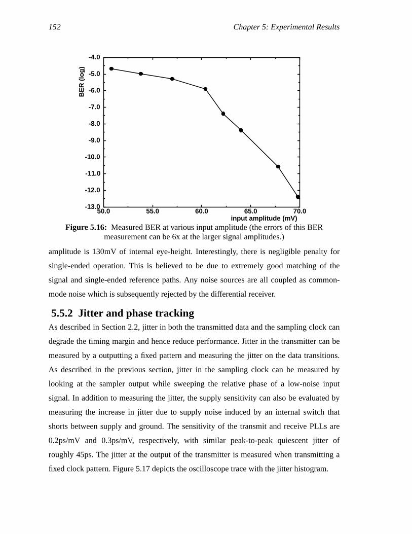
152 Chapter 5: Experimental Results
amplitude is 130mV of internal eye-height. Interestingly, there is negligible penalty for
single-ended operation. This is believed to be due to extremely good matching of the
signal and single-ended reference paths. Any noise sources are all coupled as common-
mode noise which is subsequently rejected by the differential receiver.
5.5.2 Jitter and phase trackingAs described in Section 2.2, jitter in both the transmitted data and the sampling clock can
degrade the timing margin and hence reduce performance. Jitter in the transmitter can be
measured by a outputting a fixed pattern and measuring the jitter on the data transitions.
As described in the previous section, jitter in the sampling clock can be measured by
looking at the sampler output while sweeping the relative phase of a low-noise input
signal. In addition to measuring the jitter, the supply sensitivity can also be evaluated by
measuring the increase in jitter due to supply noise induced by an internal switch that
shorts between supply and ground. The sensitivity of the transmit and receive PLLs are
0.2ps/mV and 0.3ps/mV, respectively, with similar peak-to-peak quiescent jitter of
roughly 45ps. The jitter at the output of the transmitter is measured when transmitting a
fixed clock pattern. Figure 5.17 depicts the oscilloscope trace with the jitter histogram.
Figure 5.16: Measured BER at various input amplitude (the errors of this BERmeasurement can be 6x at the larger signal amplitudes.)
input amplitude (mV)
BE
R (
log)
50.0 55.0 60.0 65.0 70.0-13.0
-12.0
-11.0
-10.0
-9.0
-8.0
-7.0
-6.0
-5.0
-4.0
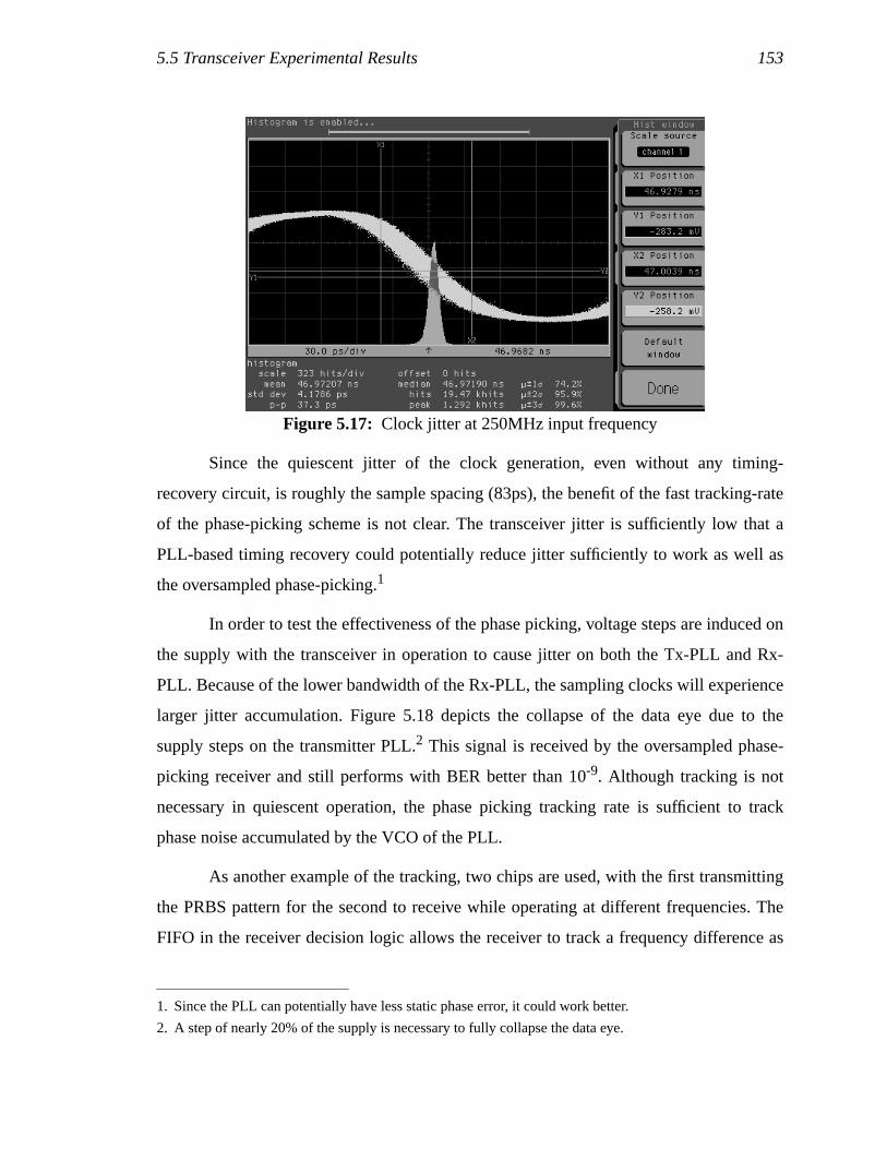
5.5 Transceiver Experimental Results 153
Since the quiescent jitter of the clock generation, even without any timing-
recovery circuit, is roughly the sample spacing (83ps), the benefit of the fast tracking-rate
of the phase-picking scheme is not clear. The transceiver jitter is sufficiently low that a
PLL-based timing recovery could potentially reduce jitter sufficiently to work as well as
the oversampled phase-picking.1
In order to test the effectiveness of the phase picking, voltage steps are induced on
the supply with the transceiver in operation to cause jitter on both the Tx-PLL and Rx-
PLL. Because of the lower bandwidth of the Rx-PLL, the sampling clocks will experience
larger jitter accumulation. Figure 5.18 depicts the collapse of the data eye due to the
supply steps on the transmitter PLL.2 This signal is received by the oversampled phase-
picking receiver and still performs with BER better than 10-9. Although tracking is not
necessary in quiescent operation, the phase picking tracking rate is sufficient to track
phase noise accumulated by the VCO of the PLL.
As another example of the tracking, two chips are used, with the first transmitting
the PRBS pattern for the second to receive while operating at different frequencies. The
FIFO in the receiver decision logic allows the receiver to track a frequency difference as
1. Since the PLL can potentially have less static phase error, it could work better.
2. A step of nearly 20% of the supply is necessary to fully collapse the data eye.
Figure 5.17: Clock jitter at 250MHz input frequency
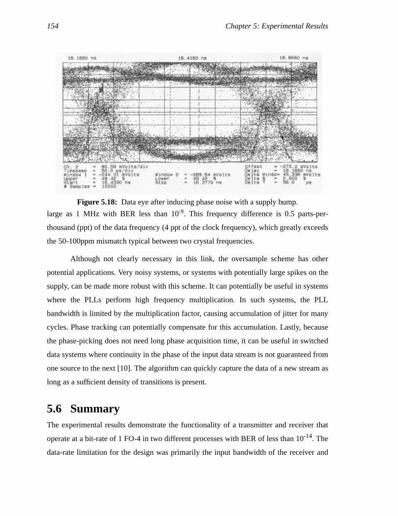
154 Chapter 5: Experimental Results
large as 1 MHz with BER less than 10-9. This frequency difference is 0.5 parts-per-
thousand (ppt) of the data frequency (4 ppt of the clock frequency), which greatly exceeds
the 50-100ppm mismatch typical between two crystal frequencies.
Although not clearly necessary in this link, the oversample scheme has other
potential applications. Very noisy systems, or systems with potentially large spikes on the
supply, can be made more robust with this scheme. It can potentially be useful in systems
where the PLLs perform high frequency multiplication. In such systems, the PLL
bandwidth is limited by the multiplication factor, causing accumulation of jitter for many
cycles. Phase tracking can potentially compensate for this accumulation. Lastly, because
the phase-picking does not need long phase acquisition time, it can be useful in switched
data systems where continuity in the phase of the input data stream is not guaranteed from
one source to the next [10]. The algorithm can quickly capture the data of a new stream as
long as a sufficient density of transitions is present.
5.6 SummaryThe experimental results demonstrate the functionality of a transmitter and receiver that
operate at a bit-rate of 1 FO-4 in two different processes with BER of less than 10-14. The
data-rate limitation for the design was primarily the input bandwidth of the receiver and
Figure 5.18: Data eye after inducing phase noise with a supply bump.
5.6 Summary 155
the on-chip clock frequency. More clock phases and larger demultiplexing may be able to
push the maximum data rate closer to the predicted maximum of 0.7 FO-4. The resolution
is limited by the input-referred offset voltages of the comparators, which were
characterized to be 100mV. This value corresponded roughly to the predicted results of the
previous chapters. The minimum receivable input eye opening while maintaining the BER
performance is 65mV (differential).
The quantization penalty of the oversampled phase-picking scheme is verified by
sweeping the phase of the input data with respect to the receiver. The performance penalty
was found to be 3dB in the worst case. The oversampled phase-picking timing-recovery
scheme is shown to be effective in tracking the phase accumulation. However the
quiescent jitter of the VCO is small enough not to require the tracking. Since the jitter is
small and the quantization error is large, a PLL-based timing recovery scheme might
perform as well with less area, power, and complexity overhead.

156 Chapter 5: Experimental Results
157
Chapter 6
Conclusion
This dissertation has shown that there are three major factors that can limit the
performance of high-speed links: clock frequency, signal bandwidth, and timing accuracy.
It uses the delay of a FO-4 inverter to measure the performance of circuits that should
scale with technology, since the limitations (in terms of FO-4) remain roughly constant
with scaling. Limitations that do not scale with technology are measured in picoseconds
and potentially establish an ultimate limit to a link’s performance.
The clock cycle-time of most chips is generally limited to roughly 8 FO-4 delay by
the clock buffer chain. To overcome this 8 FO-4 limitation, multiple bits are transmitted
and received per clock cycle, leading to the need for multiplexing at the output and
demultiplexing at the input of a high-speed link. The simplest approach, demonstrated in
many links, is to multiplex and demultiplex by 2. This leads to a bit-time performance of
3-4 FO-4. While this removes the clock-period limitation, it moves the bit-rate limitation
on the bandwidth of the multiplexing and demultiplexing circuits, and on the accuracy of
the multiple clocks.
Higher parallelism can be used to achieve higher bit rates, but requires a higher
fan-in circuit for both the receiver and the transmitter. The demultiplexing at the receiver
is performed by interleaving multiple samplers. The maximum bandwidth of the sampler
is one of the primary limitations on receiver performance. This bandwidth is limited by the
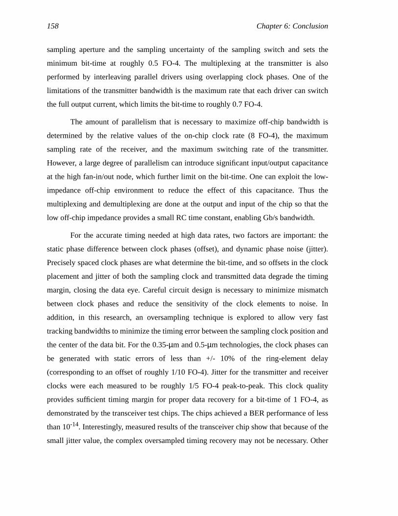
158 Chapter 6: Conclusion
sampling aperture and the sampling uncertainty of the sampling switch and sets the
minimum bit-time at roughly 0.5 FO-4. The multiplexing at the transmitter is also
performed by interleaving parallel drivers using overlapping clock phases. One of the
limitations of the transmitter bandwidth is the maximum rate that each driver can switch
the full output current, which limits the bit-time to roughly 0.7 FO-4.
The amount of parallelism that is necessary to maximize off-chip bandwidth is
determined by the relative values of the on-chip clock rate (8 FO-4), the maximum
sampling rate of the receiver, and the maximum switching rate of the transmitter.
However, a large degree of parallelism can introduce significant input/output capacitance
at the high fan-in/out node, which further limit on the bit-time. One can exploit the low-
impedance off-chip environment to reduce the effect of this capacitance. Thus the
multiplexing and demultiplexing are done at the output and input of the chip so that the
low off-chip impedance provides a small RC time constant, enabling Gb/s bandwidth.
For the accurate timing needed at high data rates, two factors are important: the
static phase difference between clock phases (offset), and dynamic phase noise (jitter).
Precisely spaced clock phases are what determine the bit-time, and so offsets in the clock
placement and jitter of both the sampling clock and transmitted data degrade the timing
margin, closing the data eye. Careful circuit design is necessary to minimize mismatch
between clock phases and reduce the sensitivity of the clock elements to noise. In
addition, in this research, an oversampling technique is explored to allow very fast
tracking bandwidths to minimize the timing error between the sampling clock position and
the center of the data bit. For the 0.35-µm and 0.5-µm technologies, the clock phases can
be generated with static errors of less than +/- 10% of the ring-element delay
(corresponding to an offset of roughly 1/10 FO-4). Jitter for the transmitter and receiver
clocks were each measured to be roughly 1/5 FO-4 peak-to-peak. This clock quality
provides sufficient timing margin for proper data recovery for a bit-time of 1 FO-4, as
demonstrated by the transceiver test chips. The chips achieved a BER performance of less
than 10-14. Interestingly, measured results of the transceiver chip show that because of the
small jitter value, the complex oversampled timing recovery may not be necessary. Other
6.1 Scaling Trends 159
timing-recovery schemes, such as a classical data-recovery PLL, can potentially achieve
similar performance.
6.1 Scaling TrendsMost, but not all, of the constraints on the speed of high-speed links scale with technology.
The primary factors, such as maximum on-chip clock-rate, receiver aperture and
transmitter switching rate, do scale because they depend on device speed and device
capacitance. This scaling is illustrated in Figure 6.1, which shows not only the scaling of
this research but also the quoted performance of other high-speed serial links along with
their respective technologies. The performance of the links falls roughly along the straight
lines which plot the approximate delays for 3 FO-4 and 1 FO-4.
There are several issues that may prevent the link speed from scaling with the FO-
4 delay, including reduced signal-to-noise ratio, jitter, static offsets scaling, and fixed
channel bandwidth limitations. These issues are described next.
Ideal scaling assumes that all voltages, including the output voltage, scale with the
supply voltage. If the output voltage does not scale, the devices used to drive the signal
Figure 6.1: Scaling of performance as technology scales
0.0 0.2 0.4 0.6 0.8 1.0 1.2feature size ( µm)
0
500
1000
1500
bit
tim
e (p
sec
)
CMOS serialBiCMOS serial
This work
[Enam]*
[Fiedler]
[Chang]
[Kim]
2000[Hu]
[Banu]
*adjusted for the f T
3 FO-4
1 FO-4
160 Chapter 6: Conclusion
will not scale, and will thus limit the bandwidth. Exacerbating thisSNR problem is that
noise, such as thermal noise, increases at higher data rates. Fortunately, this noise is a
small part of the signal amplitude even for the data rates in this research. As long as the
remaining noise sources are proportional to the signal amplitude, which is often the case
when all voltages scale, theSNR will not degrade enough to affect performance seriously
until bit-rates exceed 20Gb/s.
Jitter can be expected to scale roughly with technology as long as the input
frequency scales. The portion of jitter due to clock buffering will scale as delay scales with
technology because the jitter of a clock driven through a buffer chain is proportional to the
delay of the chain. However, if the input frequency does not scale, jitter from the a PLL
that is locked to an external clock may not scale. System constraints such as FCC
regulations often do not allow high clock frequencies on the PCB. This would require on-
chip frequency multiplication to maintain the desired clock frequency and a low input-
clock frequency. As mentioned in Chapter 4, the jitter performance does not improve
while the bit-time scales because the loop bandwidth is proportional to the input
frequency. Since jitter accumulates for greater number of bit-times, one implication is that
a clock-recovery scheme with high phase-tracking rate, such as the oversampled phase-
picking, can potentially be applicable to track the phase accumulation.
Both the static phase error and the input-offset voltage will also cause problems
when the technology scales because they are primarily due to mismatches inVT andKP.
Since device mismatches depend on the area of the device, the absolute error increases as
device size shrink. Phase spacing error will increase as a percentage of the bit-time and
thus reduce the timing margin. Similarly, the input-offset voltage will increase, limiting
input resolution and reducing the voltage margin. In addition, the aperture uncertainty due
to input-offset voltage increases, which reduces the timing margin. These offsets are
already significant enough for the 0.35-µm process technology that additional circuit
innovations will be required to cancel the offsets for future process generations.
The final, and most significant, bandwidth limitation that needs to be addressed is
the channel. Assuming that the off-chip cable and PCB have sufficient bandwidth, the
input/output capacitance does not scale ideally because a portion of the capacitance comes
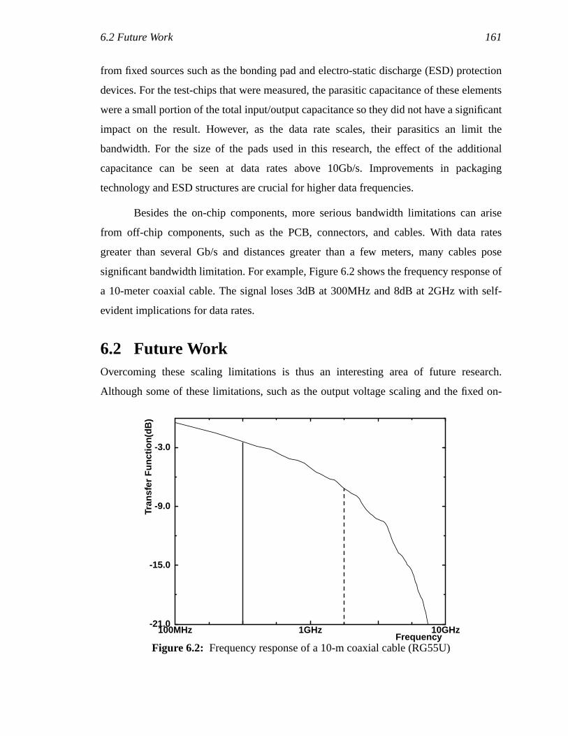
6.2 Future Work 161
from fixed sources such as the bonding pad and electro-static discharge (ESD) protection
devices. For the test-chips that were measured, the parasitic capacitance of these elements
were a small portion of the total input/output capacitance so they did not have a significant
impact on the result. However, as the data rate scales, their parasitics an limit the
bandwidth. For the size of the pads used in this research, the effect of the additional
capacitance can be seen at data rates above 10Gb/s. Improvements in packaging
technology and ESD structures are crucial for higher data frequencies.
Besides the on-chip components, more serious bandwidth limitations can arise
from off-chip components, such as the PCB, connectors, and cables. With data rates
greater than several Gb/s and distances greater than a few meters, many cables pose
significant bandwidth limitation. For example, Figure 6.2 shows the frequency response of
a 10-meter coaxial cable. The signal loses 3dB at 300MHz and 8dB at 2GHz with self-
evident implications for data rates.
6.2 Future WorkOvercoming these scaling limitations is thus an interesting area of future research.
Although some of these limitations, such as the output voltage scaling and the fixed on-
Figure 6.2: Frequency response of a 10-m coaxial cable (RG55U)
100MHz 1GHz 10GHz-21.0
-15.0
-9.0
-3.0
Tran
sfer
Fun
ctio
n(dB
)
Frequency
162 Chapter 6: Conclusion
chip I/O parasitics, are not immediate issues for scaling, others, such as device mismatch
and off-chip bandwidth limitations, need to be overcome by using clever circuits and
architectures.
One interesting area of circuit design is dealing with the transistor mismatches.
Because transistor mismatches are static (albeit random), offset-correction schemes, such
as an open-loop correction at the start-up period of the circuit, can be applied. For
example, static phase error can be corrected using programmable interpolators (as done in
[88]) that adjust each phase individually. Similarly, input-offset voltage can be corrected
using techniques commonly applied in ADCs (such as [83] and [101]). The challenge is to
perform the offset corrections with very little performance overhead for the receivers.
Because the samplers are cycled at such high rates, dynamic, closed-loop techniques can
be very difficult to apply. If these techniques can be applied, the scaling of on-chip circuit
performance can be expected to continue.
Since the scaling of CMOS provides such high bandwidths, one possible
application is toward optical interconnects where the bandwidth of the medium is
extremely high. However, electronic components to drive and receive the optical signals
have more stringent criteria than electrical links. The receivers require resolution on the
order of several millivolts and the drivers often require driving voltages greater than 3V.
The design of these circuits while scaling continues is a difficult challenge.
Electrical links are beginning to provide a higher available data bandwidth than the
off-chip environment can support. This encourages a large field of research to push high
data rates through bandwidth-limited channels. This problem has been extensively
researched for telecommunications and data communications (in published research such
as [9], [12], and [17]). Techniques such as modulation, equalization, and coding ([89], [8],
[20], [27], [46], and [90]) can provide significant improvement in data bandwidth through
transmitting more complex symbols instead of simple bits. However, applying these
techniques is challenging, especially at high symbol rates, because they require greater
voltage resolution and timing accuracy.
There is a growing interest in applying these techniques at GSym/s rates ([95],
[84], and [91]). Successful use of these techniques will demonstrate that the aggregate
6.2 Future Work 163
data rate can continue to improve with technology, even though channel-bandwidth
limitations may constrain the number of symbols per second transmitted and received.

164 Chapter 6: Conclusion
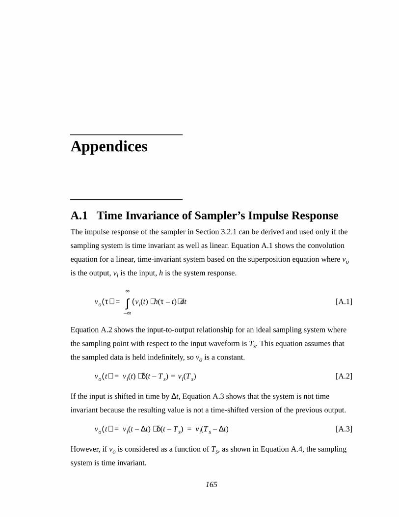
165
Appendices
A.1 Time Invariance of Sampler’s Impulse ResponseThe impulse response of the sampler in Section 3.2.1 can be derived and used only if the
sampling system is time invariant as well as linear. Equation A.1 shows the convolution
equation for a linear, time-invariant system based on the superposition equation wherevo
is the output,vi is the input,h is the system response.
[A.1]
Equation A.2 shows the input-to-output relationship for an ideal sampling system where
the sampling point with respect to the input waveform isTs. This equation assumes that
the sampled data is held indefinitely, sovo is a constant.
[A.2]
If the input is shifted in time by∆t, Equation A.3 shows that the system is not time
invariant because the resulting value is not a time-shifted version of the previous output.
[A.3]
However, ifvo is considered as a function ofTs, as shown in Equation A.4, the sampling
system is time invariant.
vo τ( ) vi t( ) h τ t–( )⋅( )∞–
∞
∫ td=
vo t( ) vi t( ) δ t Ts–( ) vi Ts( )=⋅=
vo t( ) vi t t∆–( ) δ t Ts–( )⋅ vi Ts t∆–( )= =
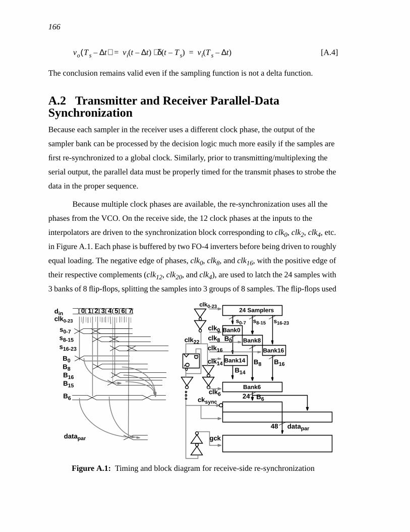
166
[A.4]
The conclusion remains valid even if the sampling function is not a delta function.
A.2 Transmitter and Receiver Parallel-DataSynchronizationBecause each sampler in the receiver uses a different clock phase, the output of the
sampler bank can be processed by the decision logic much more easily if the samples are
first re-synchronized to a global clock. Similarly, prior to transmitting/multiplexing the
serial output, the parallel data must be properly timed for the transmit phases to strobe the
data in the proper sequence.
Because multiple clock phases are available, the re-synchronization uses all the
phases from the VCO. On the receive side, the 12 clock phases at the inputs to the
interpolators are driven to the synchronization block corresponding toclk0, clk2, clk4, etc.
in Figure A.1. Each phase is buffered by two FO-4 inverters before being driven to roughly
equal loading. The negative edge of phases,clk0, clk8, andclk16, with the positive edge of
their respective complements (clk12, clk20, andclk4), are used to latch the 24 samples with
3 banks of 8 flip-flops, splitting the samples into 3 groups of 8 samples. The flip-flops used
vo Ts t∆–( ) vi t t∆–( ) δ t Ts–( )⋅ vi Ts t∆–( )= =
Figure A.1: Timing and block diagram for receive-side re-synchronization
s0-7s8-15s16-23
0 1 2 3 4 5 6 7din 24 Samplers
Bank0
s0-7 s8-15 s16-23
clk 0-23
D
Q
clk 0-23
B0B8B16B15
B0
B8 B16B14
B6 B6
48
24
datapar
datapar gck
cksync
clk 6
clk 16
clk 8
clk 0
clk 22 Bank8
Bank16
Bank14clk 14
Bank6
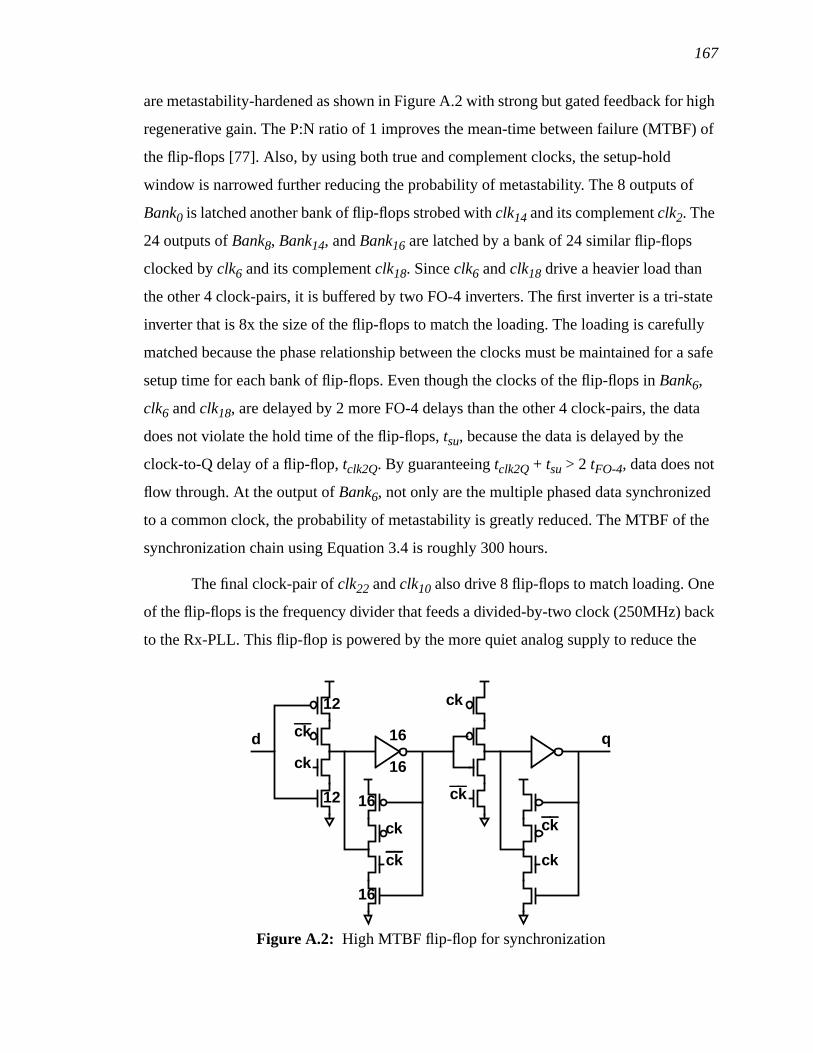
167
are metastability-hardened as shown in Figure A.2 with strong but gated feedback for high
regenerative gain. The P:N ratio of 1 improves the mean-time between failure (MTBF) of
the flip-flops [77]. Also, by using both true and complement clocks, the setup-hold
window is narrowed further reducing the probability of metastability. The 8 outputs of
Bank0 is latched another bank of flip-flops strobed withclk14 and its complementclk2. The
24 outputs ofBank8, Bank14, andBank16 are latched by a bank of 24 similar flip-flops
clocked byclk6 and its complementclk18. Sinceclk6 andclk18 drive a heavier load than
the other 4 clock-pairs, it is buffered by two FO-4 inverters. The first inverter is a tri-state
inverter that is 8x the size of the flip-flops to match the loading. The loading is carefully
matched because the phase relationship between the clocks must be maintained for a safe
setup time for each bank of flip-flops. Even though the clocks of the flip-flops inBank6,
clk6 andclk18, are delayed by 2 more FO-4 delays than the other 4 clock-pairs, the data
does not violate the hold time of the flip-flops,tsu, because the data is delayed by the
clock-to-Q delay of a flip-flop,tclk2Q. By guaranteeingtclk2Q + tsu > 2 tFO-4, data does not
flow through. At the output ofBank6, not only are the multiple phased data synchronized
to a common clock, the probability of metastability is greatly reduced. The MTBF of the
synchronization chain using Equation 3.4 is roughly 300 hours.
The final clock-pair ofclk22 andclk10 also drive 8 flip-flops to match loading. One
of the flip-flops is the frequency divider that feeds a divided-by-two clock (250MHz) back
to the Rx-PLL. This flip-flop is powered by the more quiet analog supply to reduce the
Figure A.2: High MTBF flip-flop for synchronization
ck
ck
ck
ck
ck
ck
ck
ck
d q
12
12
16
16
16
16
168
jitter. Ideally, the feedback path of the PLL should match the buffer path that generates the
clocks for the samplers, so that any on-chip induced noise with frequency beneath the loop
bandwidth can be tracked by the loop. Since the samplers are driven by only one buffer
after the low-to-high swing converter, the delay needs to be very short. The delay of this
feedback path is kept to less than 3 FO-4 so the internal input to the phase-detector is not
excessively noisy. Another one of the eight flip-flops with 2x the size is used to again
divide the clock, for the 250-MHz global logic clock. The output of the flip-flop is
buffered with inverters (with delay equivalent to 4 FO-4) to generate a clock,sync_ck, that
further demultiplexes the 24 outputs fromBank6 to 48 outputs. The remaining 5 flip-flops
are used for transceiver control signals such as reset and scan related debugging. The 24
outputs are each buffered before being driven into the demultiplexer which comprises two
flip-flops clocked by the positive and the negative edge ofsync_ck. Again, to avoid
violating the setup time of the flop, the timing requirement of 2tFO-4 + tclk2Q + tbuffer + tsu
> tclk2Q + 4tFO-4 must be satisfied. The actual global clock,gck, for the digital logic is
sync_ck, further buffered by 2 FO-4 inverters because the clock loading is so large
(extracted to be 45 pF). To guarantee that the flip-flops in the digital logic data-path do not
suffer from setup or hold time violation, these two large buffers drive the clock in the
opposite direction as the data flow. Hence, they are physically located on the side of the
chip opposite from the sampler/analog circuitry. This has the additional benefit of isolating
this large noise source from the more sensitive circuitry.
A similar re-synchronization is performed on the transmit side depicted in Figure
A.3. All 8 phases are tapped from the VCO of the Tx-PLL and buffered by one inverter.
Clock phases,calk2 andcalk6, are driven to 4 flip-flops. One acts as a toggle flip-flop to
generate the 250MHz clock,tx_gck, for the transmitter logic. Because the transmitter logic
is not very complex and hence does not impose a heavy clock load, only 2 FO-4 inverters
are necessary for clock buffering. Of the remaining 3 flip-flops, one is used for the
feedback clock for the Tx-PLL, and the other two are for testability.
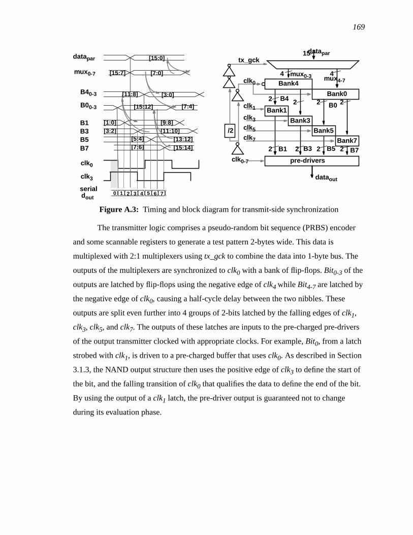
169
The transmitter logic comprises a pseudo-random bit sequence (PRBS) encoder
and some scannable registers to generate a test pattern 2-bytes wide. This data is
multiplexed with 2:1 multiplexers usingtx_gck to combine the data into 1-byte bus. The
outputs of the multiplexers are synchronized toclk0 with a bank of flip-flops.Bit0-3 of the
outputs are latched by flip-flops using the negative edge ofclk4 while Bit4-7 are latched by
the negative edge ofclk0, causing a half-cycle delay between the two nibbles. These
outputs are split even further into 4 groups of 2-bits latched by the falling edges ofclk1,
clk3, clk5, andclk7. The outputs of these latches are inputs to the pre-charged pre-drivers
of the output transmitter clocked with appropriate clocks. For example,Bit0, from a latch
strobed withclk1, is driven to a pre-charged buffer that usesclk0. As described in Section
3.1.3, the NAND output structure then uses the positive edge ofclk3 to define the start of
the bit, and the falling transition ofclk0 that qualifies the data to define the end of the bit.
By using the output of aclk1 latch, the pre-driver output is guaranteed not to change
during its evaluation phase.
Figure A.3: Timing and block diagram for transmit-side synchronization
clk 0
clk 3
0 1 2 3 4 5 6 7serial
datapar
dout
mux 0-7
B00-3
B1B3B5B7 2 222
tx_gck
clk 0
clk 1
clk 3
clk 5
clk 7
clk 0-7
/2
pre-drivers
Bank1
Bank3
Bank5
Bank7
Bank4
Bank0
datapar15
4 4
2 2 22
mux 0-3 mux 4-7
B1 B3 B5 B7
dataout
[15:0]
[7:0]
B40-3
[15:7]
[7:4]
[3:0]
[15:12]
[11:8]
[1:0][3:2]
[5:4][7:6]
[9:8][11:10]
[13:12][15:14]
B4B0
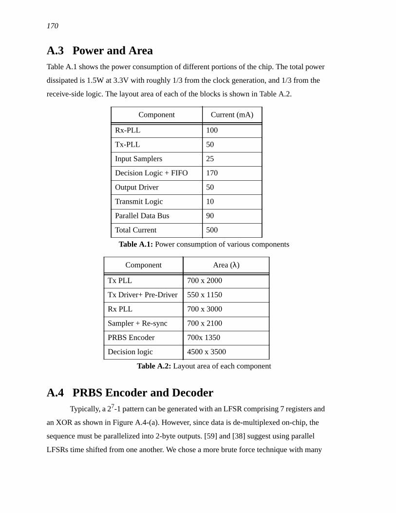
170
A.3 Power and AreaTable A.1 shows the power consumption of different portions of the chip. The total power
dissipated is 1.5W at 3.3V with roughly 1/3 from the clock generation, and 1/3 from the
receive-side logic. The layout area of each of the blocks is shown in Table A.2.
A.4 PRBS Encoder and DecoderTypically, a 27-1 pattern can be generated with an LFSR comprising 7 registers and
an XOR as shown in Figure A.4-(a). However, since data is de-multiplexed on-chip, the
sequence must be parallelized into 2-byte outputs. [59] and [38] suggest using parallel
LFSRs time shifted from one another. We chose a more brute force technique with many
Component Current (mA)
Rx-PLL 100
Tx-PLL 50
Input Samplers 25
Decision Logic + FIFO 170
Output Driver 50
Transmit Logic 10
Parallel Data Bus 90
Total Current 500
Table A.1: Power consumption of various components
Component Area (λ)
Tx PLL 700 x 2000
Tx Driver+ Pre-Driver 550 x 1150
Rx PLL 700 x 3000
Sampler + Re-sync 700 x 2100
PRBS Encoder 700x 1350
Decision logic 4500 x 3500
Table A.2: Layout area of each component
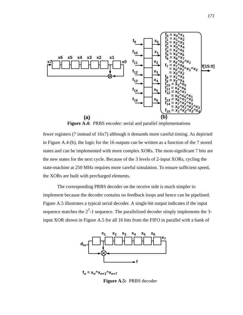
171
fewer registers (7 instead of 16x7) although it demands more careful timing. As depicted
in Figure A.4-(b), the logic for the 16 outputs can be written as a function of the 7 stored
states and can be implemented with more complex XORs. The most-significant 7 bits are
the new states for the next cycle. Because of the 3 levels of 2-input XORs, cycling the
state-machine at 250 MHz requires more careful simulation. To ensure sufficient speed,
the XORs are built with precharged elements.
The corresponding PRBS decoder on the receive side is much simpler to
implement because the decoder contains no feedback loops and hence can be pipelined.
Figure A.5 illustrates a typical serial decoder. A single-bit output indicates if the input
sequence matches the 27-1 sequence. The parallelized decoder simply implements the 3-
input XOR shown in Figure A.5 for all 16 bits from the FIFO in parallel with a bank of
Figure A.4: PRBS encoder: serial and parallel implementations
f0 = x0^x 1f1 = x1^x 2f2 = x2^x 3f3 = x3^x 4f4 = x4^x 5f5 = x5^x 6f6 = x6^x 7
f7 = x7^x 8
f8 = x1^x 3f9 = x2^x 4f10 = x3^x 5f11 = x4^x 6f12 = x5^x 7
f13 = x6^x 1^x 2f14 = x7^x 2^x 3
f15 = x1^x 2^x 3^x 4
= x6^x 0^x 1
= x0^x 1^x 1^x 2= x0^x 2
= x5^x 0^x 1
= x0^x 1^x 2^x 3
f9
f10
f11
f12
f13
f14
f15
x0
x1
x2
x3
x4
x5
x6
x0x1x2x3x4x5x6
x7f[15:0]
(a) (b)
Figure A.5: PRBS decoder
fn = xn^x n+1^x n+7
din
x1 x2 x3 x4 x5 x6x7
f
172
XORs. To generate a single error flag as output, the XOR outputs are OR-ed together so
that a high-value from any of the XORs triggers the flag. Although this potentially masks
multiple errors per byte, this is sufficient for low bit-error-rate measurements.
173
Bibliography
[1] M. Afghahi, et al., “A unified single-phase clocking scheme for VLSI systems,”
IEEE Journal of Solid-State Circuits, Feb. 1990, vol.25, no.1, pp. 225-33
[2] J. Alvarez, et al., “A wide-bandwidth low-voltage PLL for PowerPC
microprocessors,”IEEE Journal of Solid-State Circuits, Apr. 1995, vol.30, no.4,
pp. 383-91
[3] R. Ammar, C. Ajouri, “GTL: a low-swing solution for high-speed digital logic,”
Proceedings of WESCON95, San Francisco, Nov. 1995.
[4] L. Andersson et al., “Silicon Bipolar Chipset for SONET/SDH 10 Gb/s Fiber-
Optic Communication Links,” IEEE Journal of Solid-State Circuits, Mar. 1995,
vol.30, no.3, pp. 210-8
[5] P.V. Argade, “Sizing an Inverter with a Precise Delay: Generation of
Complementary Signals with Minimal Skew and Pulsewidth Distortion in CMOS,”
IEEE Transactions on Computer Aided Design of Integrated Circuits and Systems,
Jan. 1989, vol.8, no.1, pp. 33-44
[6] M. Banu, A. Dunlop, “A 660Mb/s CMOS Clock Recovery Circuit with
Instantaneous Locking for NRZ Data and Burst-Mode Transmission,”1993
International Solid State Circuits Conference. Digest of Technical Papers, Feb.
1993, pp. 102-3
174 Bibliography
[7] R. Best, Phase-Locked Loops, 3rd ed, McGraw Hill, 1997
[8] P.J. Black, et al., “A 1-Gb/s, four-state, sliding block Viterbi decoder,”IEEE
Journal of Solid-State Circuits, Jun. 1997, vol.32, no.6, p. 797-805
[9] J. Boxho, et al., “An analog front end for multi-standard power line carrier
modem,”1997 IEEE International Solid-State Circuits Conference. Digest of
Technical Papers. Feb. 1997, p. 84-5
[10] M. Cerisola, et al., “CORD - A WDM Optical Network: Control Mechanism
Using Subcarrier Multiplexing and Novel Synchronization Solutions,”IEEE
International Conference on Communication, 1995, pp 261-5
[11] K.Y. Chang, et al., “A 2-Gb/s Asymmetric Link for High-Bandwidth Packet
Switches,”Hot Interconnects V Symposium Record, Aug. 1997, pp. 171-9
[12] Z.Y. Chang, et al, “A CMOS Analog Front-End Circuit for an FDM-Based ADSL
System,”IEEE Journal of Solid-State Circuits, Dec. 1995, vol.30, no.12, pp. 1449-
56
[13] D.L. Chen, R. Waldron, “A Single-Chip 266Mb/s CMOS Transmitter/Receiver for
Serial Data Communications,”1993 IEEE International Solid-State Circuits
Conference. Digest of Technical Papers. Feb. 1993, pp. 100-1
[14] K. Chen, et al., “Predicting CMOS Speed with Gate Oxide and Voltage Scaling
and Interconnect Loading Effects,”IEEE Transactions on Electron Device. Nov.
1997, vol.44, no.11, pp. 1951-7
[15] J. Christiansen, “An Integrated High Resolution CMOS Timing Generator Based
on an Array of Delay Locked Loops,”IEEE Journal of Solid-State Circuits, Jul.
1996, vol.31, no.7, pp. 952-7
[16] R. Co, J.H. Mulligan Jr., “Optimization of Phase-Locked Loop Performance in
Data Recovery Systems,”IEEE Journal of Solid-State Circuits, Sep. 1994, vol.29,
no.9, pp. 1022-34
[17] M. Combe, et al., “A second-generation modem analog front-end,”1992 IEEE
International Solid-State Circuits Conference. Digest of Technical Papers. Feb.
1992, pp. 224-5, 290
175
[18] Connecting Device Inc, Microwave Connectors and Cable Assemblies, pp. 123
[19] M. Cooperman, P. Andrade, “CMOS Gigabit-per-Second Switching,”IEEE
Journal of Solid-State Circuits, Jun. 1993, vol.28, no.6, pp. 631-9
[20] W.J. Dally, et al., “Transmitter equalization for 4-Gbps signaling,”IEEE Micro,
Jan.-Feb. 1997, vol.17, no.1, p. 48-56
[21] A. DeHon, T. Knight Jr., T. Simon, “Automatic Impedance Control,”1993 IEEE
International Solid-State Circuits Conference. Digest of Technical Papers. Feb.
1993, pp. 164-5
[22] M. Dolle, “A Dynamic Line-Termination Circuit for Multireceiver Nets,”IEEE
Journal of Solid-State Circuits, Dec. 1996, vol.28 no.12, pp. 1370
[23] K.S. Donnelly, et al., “A 660-MB/s interface megacell portable circuit in 0.3-µm-
0.7-µm CMOS ASIC,”IEEE Journal of Solid-State Circuits, Dec. 1996, vol.31,
no.12 p. 1995-2003
[24] C.A. Eldering, et al., “Digital Burst Mode Clock Recovery Technique for Fiber-
Optic Systems,”IEEE Journal of Solid-State Circuits, Feb. 1994, vol.29, no.2, pp.
271
[25] S.K. Enam, A.A. Abidi, “NMOS IC’s for Clock and Data Regeneration in Gigabit-
per-Second Optical-Fiber Receivers,” IEEE Journal of Solid State Circuits, Dec.
1992, vol.27, no.12, pp. 1763-74
[26] J.F. Ewen, et al., “Single-Chip 1062MBaud CMOS Transceiver for Serial Data
Communication,”1995 IEEE International Solid-State Circuits Conference.
Digest of Technical Papers. Feb. 1995, pp. 32-3
[27] R. Farjad-Rad, et al., “An Equalization Scheme for 10-Gb/s 4-PAM Signaling over
Long Cables,”Mixed Signal Conference, Jul. 1997, Cancun, Mexico.
[28] A. Fiedler, et al., “A 1.0625 Gbps transceiver with 2x-oversampling and transmit
signal pre-emphasis,”1997 IEEE International Solids-State Circuits Conference.
Digest of Technical Papers Feb. 1997, pp. 238-9
[29] R.C. Foss, et al., “Memory- fast interfaced for DRAMs,”IEEE Spectrum, Oct.
1992, vol.29, no.10, pp. 54-7
176 Bibliography
[30] M. Galles, et al., “Spider: a high-speed network interconnect,”IEEE Micro Jan.-
Feb. 1997, vol.17, no.1, p. 34-9
[31] F.M. Gardner, “Charge-pump phase-lock loops,”IEEE Transactions on
Communications, Nov. 1980, vol.COM-28, no.11, p. 1849-58
[32] F. Gardner,Phase Lock Techniques, Wiley 1979
[33] C. Gray, et al., “A Sampling Technique and Its CMOS Implementation with 1-Gb/
s Bandwidth and 25ps Resolution,” IEEE Journal of Solid State Circuits, Mar. 1994,
vol.29, no.3, pp. 340-9
[34] P. Gray, “Presentation, Short Course,”1997 International Solid-State Circuits
Conference Short Course, Feb. 1997
[35] A. Hajimiri, T.H. Lee, “A General Theory of Phase Noise in Electrical
Oscillators,”IEEE Journal of Solid-State Circuits, Feb. 1998, vol.33. no.2, pp.
179-94
[36] H.I. Hanafi, et al., “Design and Characterization of a CMOS Off-Chip Driver/
Receiver with Redced Power/Supply Disturbance,”IEEE Journal of Solid-State
Circuits, May 1992, vol.27. no.5, p. 783-90
[37] M.A. Horowitz, et al., “PLL Design for a 500MB/s Interface,”1993 International
Solid-State Circuits Conference, Digest of Technical Papers, Feb. 1993, pp. 160-1
[38] M.Y. Hsiao, K.Y. Sih, “Serial-to-Parallel Transformation of Linear-Feedback
Shift-Register Circuits,”IEEE Transaction on Electronic Computers, Dec. 1968,
pp 738-40
[39] T.H. Hu, et al., “A monolithic 480 Mb/s parallel AGC/decision/clock-recovery
circuit in 1.2-µm CMOS,”IEEE Journal of Solid-State Circuits, Dec. 1993, vol.28,
no.12, p. 1314-20
[40] M. Ishibe, et al., "High-Speed CMOS I/O Buffer Circuits,"IEEE Journal of Solid-
State Circuits, Apr. 1992, vol.27, no.4, pp. 671-3
[41] N. Ishihara, et al., “3.5-Gb/s x 4-Ch Si bipolar LSI’s for Optical Interconnections,”
IEEE Journal of Solid-State Circuits, Dec. 1995, vol.30, no.12, pp. 1493-1501
177
[42] M.J. Izzard, C.G. Thisell, “Low Power Analog Control Clock Synchronizer for
3Gb/s Data Retiming in ATM Applications,”TI ACS Report, Nov. 1994.
[43] D.K. Jeong, et al., “Design of PLL-based clock generation circuits,”IEEE Journal
of Solid-State Circuits, April 1987, vol.SC-22, no.2, p. 255-61
[44] H.O. Johansson,CMOS Parallel-Sampling Receivers, PhD Dissertation,
Linkoping University, Sweden 1998.
[45] H.O. Johansson, J. Yuan, C. Svensson, “A 4-GSamp/s Line-Receiver in 0.8µm
CMOS,” 1996 Symposium on VLSI Circuits. Digest of Technical Papers, Jun.
1996, pp. 116-7
[46] D.A. Johns, D. Essig, “Integrated Circuits for Data Trasmission Over Twisted-Pair
Channels,”IEEE Journal of Solid-State Circuits, Mar. 1997, vol.32, no.3, pp. 398-
406
[47] M.G. Johnson, et al., “A variable delay line PLL for CPU-coprocessor
synchronization,”IEEE Journal of Solid-State Circuits, Oct. 1988, vol.23, no.5, p.
1218-23
[48] B. Kim, et al., “A 30-MHz hybrid analog/digital clock recovery circuit in 2-µm
CMOS,” IEEE Journal of Solid-State Circuits, Dec. 1990, vol.25, no.6, p. 1385-94.
[49] S. Kim, et al., “An 800Mbps Multi-Channel CMOS Serial Link with 3x
Oversampling,”IEEE 1995 Custom Integrated Circuits Conference Proceedings,
Feb. 1995, pp. 451.
[50] M. Kurisu, et al., “2.8-Gb/s 176-mW Byte-Interleaved and 3.0-Gb/s 118-mW Bit-
Interleaved 8:1 Multiplexers with a 0.15-µm CMOS Technology,”IEEE Journal of
Solid-State Circuits, Dec. 1996, vol.31, no.12, pp. 2024-9
[51] N. Kushiyama, et al., “A 500-megabyte/s data-rate 4.5 M DRAM,” IEEE Journal
of Solid-State Circuits, Apr. 1993. vol.28, no.4, p. 490-8
[52] J. Kuskin, et al., "The Stanford FLASH Multiprocessor,"Proceedings of the 21st
International Symposium on Computer Architecture, Chicago, IL, Apr. 1994, pp.
302-13
178 Bibliography
[53] Z. Lao, U. Langmann, “Design of a Low-Power 10Gb/s Si Bipolar 1:16
Demultiplexer IC,”IEEE Journal of Solid-State Circuits, Jan. 1996, vol.31, no.1,
pp. 128-31
[54] S.J. Lee, B. Kim, K. Lee, “A Novel High Speed Ring Oscillator for Multi-Phase
Clock Generation Using Negative Skewed Delay Scheme,”IEEE Journal of Solid-
State Circuits, Feb. 1997, vol.32, no.2, pp. 289-91
[55] K. Lee, et al., “A CMOS serial link for fully duplexed data communication,”IEEE
Journal of Solid-State Circuits, Apr. 1995, vol.30, no.4, p. 353-64
[56] T.H. Lee, et al., “A 2.5 V CMOS delay-locked loop for 18 Mbit, 500 megabyte/s
DRAM,” IEEE Journal of Solid-State Circuits, Dec. 1994, vol.29, no.12, p. 1491-6
[57] T.H. Lee, J. Bulzachelli, “A 155MHz Clock Recovery Delay-and Phase-Locked
Loop,” IEEE Journal of Solid-State Circuits, Dec. 1992, vol.27, no.12, p. 1736
[58] A. Le Fevre, R. Flett, “A 100Mb/s Multi-LAN Crosspoint Chip-Set for Cable
Management,”IEEE Journal of Solid-State Circuits, Jul. 1997, vol.32, no.7, pp.
1115-1121
[59] A. Lempel, W.L. Eastman, “High Speed Generation of Maximal Length
Sequences,”IEEE Transaction on Computers, Feb. 1971, vol. C-20, no.2, pp 227-9
[60] A. Leon-Garcia,Probability and Random Processes for Electrial Engineering,
Addison-Wesley Publishing Co., New York, 1994
[61] S.I. Long, J.Q. Zhang, "Low Power GaAs Current-Mode 1.2Gb/s Interchip
Interconnections,”IEEE Journal of Solid-State Circuits, Jun. 1997, vol.32, no.6,
pp. 890-7
[62] W.T. Lynch, H.J. Boll, “Optimization of the Latching Pulse for Dynamic Flip-Flop
Sensors,”IEEE Journal of Solid-State Circuits, Apr. 1974, vol.9, no.2, pp. 49-55
[63] J.G. Maneatis, et al., “Low-jitter process-independent DLL and PLL based on self-
biased techniques”IEEE Journal of Solid-State Circuits, Nov. 1996. vol.31, no.11,
p. 1723-32
[64] J.G. Maneatis, et al., “Precise delay generation using coupled oscillators,”IEEE
Journal of Solid-State Circuits, Dec. 1993, vol.28, no.12, p. 1273-82
179
[65] R. Matick,Transmission lines for digital and communication networks 3rd ed.,
IEEE Press, 1997
[66] J.E. McNamara,Technical Aspects of Data Communication, 2nd ed. Digital Press,
Bedford, MA, 1982.
[67] J.A. McNeill, “Jitter in Ring Oscillators,”IEEE Journal of Solid-State Circuits,
Jun. 1997, vol.32, no.6, pp. 870-9
[68] D.G. Messerschmit, “Synchronization in Digital System Design,”IEEE Journal in
Selected Areas in Communications, Oct. 1990, vol.8, no.8, pp. 1404-19
[69] T. Mizuno, “Experimental study of threshold voltage fluctuation due to statistical
variation of channel dopant number in MOSFET’s,"IEEE Transactions on
Electron Devices, Nov. 1994, vol.41, no.11, pp. 2216-21
[70] R. Mooney, et al., “A 900 Mb/s bidirectional signaling scheme,”IEEE Journal of
Solid-State Circuits,Dec. 1995, vol.30, no.12, p. 1538-43
[71] Motorola Inc.,MECL Data Book
[72] G.C. Moyer, et al., “The delay vernier pattern generation technique,”IEEE Journal
of Solid-State Circuits, April 1997, vol.32, no.4, p. 551-62
[73] K. Nakamura, et al., “A 6-Gbps CMOS Phase Detectig DEMUX Module Using
Half-Frequency Clock,”1998 Symposium on VLSI Circuits. Digest of Technical
Papers, Jun. 1998, pp. 196-7
[74] M. Ohuchi, et al, “A Si Bipolar 5-Gb/s 8:1 Multiplexer and 4.2-Gb/s 1:8
Demultiplexer,”IEEE Journal of Solid-State Circuits, Apr. 1992, vol.27, no.4, pp.
664-7
[75] Y. Ota, R.G. Swartz, “Multichannel Parallel Data Link for Optical
Communication,”IEEE LTS, May. 1991, vol.2, no.2, pp. 24-32
[76] M.J. Pelgrom, “Matching Properties of MOS Transistors,”IEEE Journal of Solid
State Circuits,Oct. 1989, vol. 24, no. 10, pp. 1433-9
180 Bibliography
[77] C.L. Portmann, et al., “Metastability in CMOS library elements in reduced supply
and technology scaled applications,”IEEE Journal of Solid State Circuits,Jan.
1995, vol. 30, no. 1, pp. 39-46
[78] J. Poulton, et al., “A Tracking Clock Recovery Receiver for 4-Gb/s Signaling,”Hot
Interconnects V Symposium Record, Aug. 1997, Stanford, pp. 157-69
[79] B. Prince,Semiconductor Memories: A Handbook of Design, Manufacture, and
Application, John Wiley & Sons, West Sussex, England, 1991
[80] J. Proakis, M. Salehi,Communication Systems Engineering, Prentice Hall, New
Jersey, 1994
[81] M. Rau, et al., “Clock/Data Recovery PLL Using Half-Frequency Clock,”IEEE
Journal of Solid-State Circuits, Jul. 1997, vol.32, no.7, pp. 1156-9
[82] B. Razavi, Editor,Monolithic Phase Locked Loops and Clock Recovery Circuits,
IEEE Press, 1996.
[83] B. Razavi, B.A. Wooley, “Design Techniques for High-Speed, High-Resolution
Comparators,”IEEE Journal of Solid-State Circuits, Dec. 1992, vol.27, no.12, pp.
1916-26
[84] D. Reynolds, “A 320 MHz CMOS Triple 8 bit DAC with PLL,”IEEE Journal of
Solid-State Circuits, Dec. 1994, vol 29, no.12, pp. 1545
[85] T. Sekiguchi, et al., “Low-Noise, High-Speed Data Transmission Using a Ringing-
Cancelling Output Buffer,”IEEE Journal of Solid-State Circuits, Nov. 1995,
vol.30, no.12, pp. 1569-74
[86] S. Sidiropoulos, et al., “A CMOS 500 Mbps/pin synchronous point to point link
interface,”Proceedings of 1994 IEEE Symposium on VLSI Circuits. Digest of
Technical Papers, pp. 43-4
[87] S. Sidiropoulos, et al., “A 700-Mb/s/pin CMOS signaling interface using current
integrating receivers,”IEEE Journal of Solid-State Circuits, May 1997, vol.32,
no.5, pp. 681-90
[88] S. Sidiropoulos, M.A. Horowitz, “A Semidigital Dual Delay-Locked Loop,”IEEE
Journal of Solid-State Circuits, Nov. 1997, vol.32, no.11, pp. 1683-92
181
[89] B. Sklar,Digital Communications Fundamentals and Applications, Prentice Hall
1988 Englewood Cliffs, New Jersey
[90] B.S. Song, et al., “NRZ timing recovery technique for band limited channels,”
1996 IEEE International Solid-State Circuits Conference. Digest of Technical
Papers, pp. 194-5.
[91] J. Spalding, et al., “A 200M sample/s 6b flash ADC in 0.6µm CMOS,”1996 IEEE
International Solid-State Circuits Conference. Digest of Technical Papers, pp. 320-
1.
[92] R.G. Swartz, et al., “A Burst mode, Packet Receiver with Precision Reset and
Automatic Dark Level Compensation for Optical Bus Communications,”IEEE
Journal of Solid-State Circuits, Feb. 1994, vol.29, no.2, pp. 325
[93] T. Takahashi, et al., “A CMOS Gate Array with 600 Mb/s Simultaneous
Bidirectional I/O Circuits,”IEEE Journal of Solid State Circuits, Dec. 1995, vol.
30, no. 12. pp. 1544-46
[94] G.O. Thompson, “Work progresses on gigabit Ethernet,”Computer IEEE Comput.
Soc, May 1997, vol.30, no.5, pp. 95-6
[95] R. Van de Plassche,Integrated Analog-to-Digital and Digital-to-Analog
Converters, Kluwer Academic Publishers, 1994.
[96] R.C. Walker, et al, “A 1.5-Gb/s link interface chipset for computer data
transmission,”IEEE Journal of Solid-State Circuits, Jun. 1991, vol.26, no.6, pp.
698-703
[97] N.H.E. Weste, K. Eshraghian,Principles of CMOS VLSI Design A Systems
Perspective, 2nd Edition, Addison Wesley, Menlo Park, CA. 1993
[98] I.J. Wickelgren, “The facts about FireWire [serial communication bus],”IEEE
Spectrum,Apr. 1997, vol.34, no.4, pp. 19-25
[99] A.X. Widmer, et al., “Single-chip 4*500-MBd CMOS transceiver,”IEEE Journal
of Solid-State Circuits,Dec. 1996, vol.31, no.12, pp. 2004-14
[100] A.X. Widmer, P.A. Franaszek, “A DC-Balanced Partitioned-Block 8B/10B
Transmission Code,”IBM Journal R&D,Sep 1983, vol.27, pp. 440-51
182 Bibliography
[101] J.T. Wu, et al., “A 100-MHz pipelined CMOS comparator,”IEEE Journal of Solid-
State Circuits, Jun. 1988, vol. 23, no.6, pp. 1379-85
[102] C.K. Yang, et al., “A 0.6-µm CMOS 4 Gbps Transceiver with Data Recovery using
Oversampling,”Proceedings of 1997 IEEE Symposium on VLSI Circuits. Digest of
Technical Papers, Jun. 1997, pp. 71-2
[103] C.K. Yang, et al., “A 0.8-µm CMOS 2.5 Gb/s oversampling receiver and
transmitter for serial links,"IEEE Journal of Solid-State Circuits, Dec. 1996,
vol.31, no.12, pp. 2015-23
[104] I.A. Young, et al., “A PLL clock generator with 5 to 110 MHz lock range for
microprocessors,”IEEE Journal of Solid-State Circuits, Nov. 1992, vol.27, no.11,
pp. 1599-607
[105] A. Yukawa, et al., “A CMOS 8-bit high speed A/D converter IC,”1988
Proceedings of the Tenth European Solid-State Circuits Conference, pp. 193-6


![STRIWORD ELE~TROIIICS LIBORRTORIESi.stanford.edu/pub/cstr/reports/csl/tr/75/98/CSL-TR-75-98.pdf · The reader is assumed familiar with both*he Palyn EMMY [1], the IBM System/360 [3],](https://img.pdfslide.us/doc/110x75/5ea2650912738b1f43750d11/striword-eletroiiics-the-reader-is-assumed-familiar-with-bothhe-palyn-emmy-1.jpg)