Embed Size (px)
DESCRIPTION
This document investigates the design of Gilbert Cell.The process includes explanation of basic concepts like Long TailPair and using it to implement the Analog multiplier circuit. Thesoftware used for simulation is LT Spice IV version 4.08u withpreloaded cell library. The final objective is to design amultiplier giving +/1 10 V output for +/- 5V input
Citation preview
1
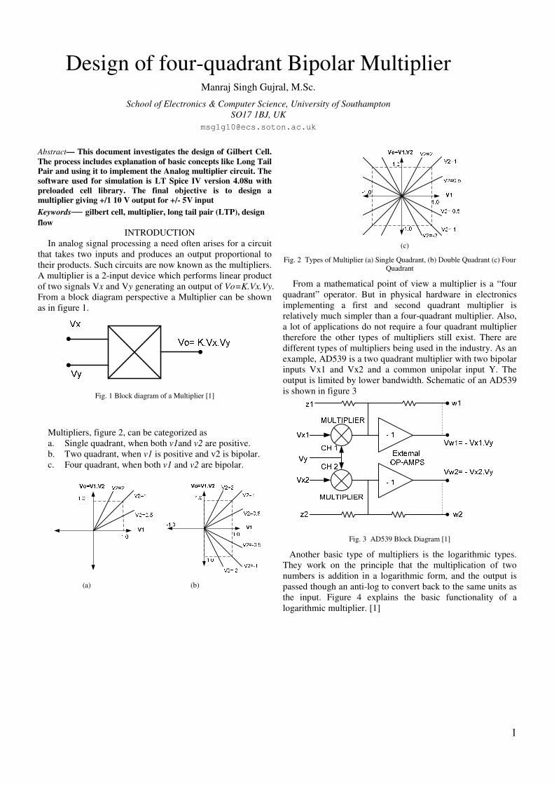
Design of four-quadrant Bipolar Multiplier Manraj Singh Gujral, M.Sc.
School of Electronics & Computer Science, University of Southampton
SO17 1BJ, UK
Abstract— This document investigates the design of Gilbert Cell.
The process includes explanation of basic concepts like Long Tail
Pair and using it to implement the Analog multiplier circuit. The
software used for simulation is LT Spice IV version 4.08u with
preloaded cell library. The final objective is to design a
multiplier giving +/1 10 V output for +/- 5V input
Keywords— gilbert cell, multiplier, long tail pair (LTP), design
flow INTRODUCTION
In analog signal processing a need often arises for a circuit
that takes two inputs and produces an output proportional to
their products. Such circuits are now known as the multipliers.
A multiplier is a 2-input device which performs linear product
of two signals Vx and Vy generating an output of Vo=K.Vx.Vy.
From a block diagram perspective a Multiplier can be shown
as in figure 1.
Fig. 1 Block diagram of a Multiplier [1]
Multipliers, figure 2, can be categorized as
a. Single quadrant, when both v1and v2 are positive.
b. Two quadrant, when v1 is positive and v2 is bipolar.
c. Four quadrant, when both v1 and v2 are bipolar.
(c)
Fig. 2 Types of Multiplier (a) Single Quadrant, (b) Double Quadrant (c) Four
Quadrant
From a mathematical point of view a multiplier is a “four
quadrant” operator. But in physical hardware in electronics
implementing a first and second quadrant multiplier is
relatively much simpler than a four-quadrant multiplier. Also,
a lot of applications do not require a four quadrant multiplier
therefore the other types of multipliers still exist. There are
different types of multipliers being used in the industry. As an
example, AD539 is a two quadrant multiplier with two bipolar
inputs Vx1 and Vx2 and a common unipolar input Y. The
output is limited by lower bandwidth. Schematic of an AD539
is shown in figure 3
Fig. 3 AD539 Block Diagram [1]
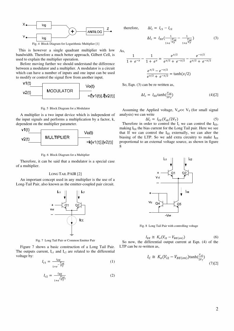
Another basic type of multipliers is the logarithmic types.
They work on the principle that the multiplication of two
numbers is addition in a logarithmic form, and the output is
passed though an anti-log to convert back to the same units as
the input. Figure 4 explains the basic functionality of a
logarithmic multiplier. [1]
(a) (b)
2
Fig. 4 Block Diagram for Logarithmic Multiplier [1]
This is however a single quadrant multiplier with low
bandwidth. Therefore a much better approach, Gilbert Cell, is
used to explain the multiplier operation.
Before moving further we should understand the difference
between a modulator and a multiplier. A modulator is a circuit
which can have a number of inputs and one input can be used
to modify or control the signal flow from another input.
Fig. 5 Block Diagram for a Modulator
A multiplier is a two input device which is independent of
the input signals and performs a multiplication by a factor, k,
dependent on the multiplier parameter.
Fig. 6 Block Diagram for a Multiplier
Therefore, it can be said that a modulator is a special case
of a multiplier.
LONG TAIL PAIR [2]
An important concept used in any multiplier is the use of a
Long-Tail Pair, also known as the emitter-coupled pair circuit.
Fig. 7 Long Tail Pair or Common Emitter Pair
Figure 7 shows a basic construction of a Long Tail Pair.
The outputs current, Ic1 and Ic2 are related to the differential
voltage by:
��� = �����
�� �� (1)
��� = �����(
�� �� ) (2)
therefore, ∆�� = ��� − ���
∆�� = ���( �
���� ��
− �
���� ��
) (3)
As,
11 +��� − 1
1 +�� = ��/���/� +���/� −
���/���/� +���/�
��/� − ���/���/� +���/� = tanh(�/2)
So, Eqn. (3) can be re-written as,
∆�� = ���tanh(!� �!�) (4)[2]
Assuming the Applied voltage, Vid<< VT (for small signal
analysis) we can write
∆�� = ���("#$/2"%) (5)
Therefore in order to control the Ic we can control the IEE,
making IEE the bias current for the Long Tail pair. Here we see
that If we can control the IEE externally, we can alter the
biasing of the LTP. So we add extra circuitry to make IEE
proportional to an external voltage source, as shown in figure
8
Fig. 8 Long Tail Pair with controlling voltage
��� ≅'(("#� − ")�((*)) (6)
So now, the differential output current at Eqn. (4) of the
LTP can be re-written as,
�+ ≅'(("#� − ")�((*))tanh(",-2".)
(7)[2]
3
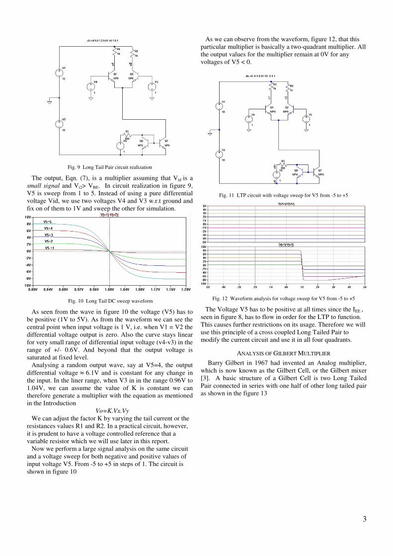
Fig. 9 Long Tail Pair circuit realization
The output, Eqn. (7), is a multiplier assuming that Vid is a
small signal and Vi2> VBE. In circuit realization in figure 9,
V5 is sweep from 1 to 5. Instead of using a pure differential
voltage Vid, we use two voltages V4 and V3 w.r.t ground and
fix on of them to 1V and sweep the other for simulation.
Fig. 10 Long Tail DC sweep waveform
As seen from the wave in figure 10 the voltage (V5) has to
be positive (1V to 5V). As from the waveform we can see the
central point when input voltage is 1 V, i.e. when V1 = V2 the
differential voltage output is zero. Also the curve stays linear
for very small range of differential input voltage (v4-v3) in the
range of +/- 0.6V. And beyond that the output voltage is
saturated at fixed level.
Analysing a random output wave, say at V5=4, the output
differential voltage/6.1V and is constant for any change in
the input. In the liner range, when V3 in in the range 0.96V to
1.04V, we can assume the value of K is constant we can
therefore generate a multiplier with the equation as mentioned
in the Introduction
Vo=K.Vx.Vy
We can adjust the factor K by varying the tail current or the
resistances values R1 and R2. In a practical circuit, however,
it is prudent to have a voltage controlled reference that a
variable resistor which we will use later in this report.
Now we perform a large signal analysis on the same circuit
and a voltage sweep for both negative and positive values of
input voltage V5. From -5 to +5 in steps of 1. The circuit is
shown in figure 10
As we can observe from the waveform, figure 12, that this
particular multiplier is basically a two-quadrant multiplier. All
the output values for the multiplier remain at 0V for any
voltages of V5 < 0.
Fig. 11 LTP circuit with voltage sweep for V5 from -5 to +5
Fig. 12 Waveform analysis for voltage sweep for V5 from -5 to +5
The Voltage V5 has to be positive at all times since the IEE ,
seen in figure 8, has to flow in order for the LTP to function.
This causes further restrictions on its usage. Therefore we will
use this principle of a cross coupled Long Tailed Pair to
modify the current circuit and use it in all four quadrants.
ANALYSIS OF GILBERT MULTIPLIER
Barry Gilbert in 1967 had invented an Analog multiplier,
which is now known as the Gilbert Cell, or the Gilbert mixer
[3]. A basic structure of a Gilbert Cell is two Long Tailed
Pair connected in series with one half of other long tailed pair
as shown in the figure 13
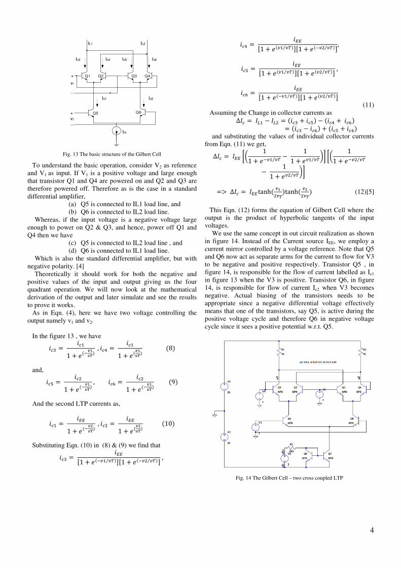
4
Ic3 Ic4
v1
+
_
Q1 Q2
+
_v2
Ic1
Q5 Q6
Ic5 Ic6
Q3 Q4
Ic2
IEE
IL1 IL2
Fig. 13 The basic structure of the Gilbert Cell
To understand the basic operation, consider V2 as reference
and V1 as input. If V1 is a positive voltage and large enough
that transistor Q1 and Q4 are powered on and Q2 and Q3 are
therefore powered off. Therefore as is the case in a standard
differential amplifier,
(a) Q5 is connected to IL1 load line, and
(b) Q6 is connected to IL2 load line.
Whereas, if the input voltage is a negative voltage large
enough to power on Q2 & Q3, and hence, power off Q1 and
Q4 then we have
(c) Q5 is connected to IL2 load line , and
(d) Q6 is connected to IL1 load line.
Which is also the standard differential amplifier, but with
negative polarity. [4]
Theoretically it should work for both the negative and
positive values of the input and output giving us the four
quadrant operation. We will now look at the mathematical
derivation of the output and later simulate and see the results
to prove it works.
As in Eqn. (4), here we have two voltage controlling the
output namely v1 and v2.
In the figure 13 , we have
,�0 = ,��1 + �(�12
1�) , ,�4 = ,��
1 + �(121�)(8)
and,
,�6 = ,��1 + �(�12
1�), ,�7 = ,��
1 + �(�121�)
(9)
And the second LTP currents as,
,�� = ,��1 + �(�19
1�) , ,�� = ,��
1 + �(191�)(10)
Substituting Eqn. (10) in (8) & (9) we find that
,�0 = ,��;1 + �(�<� <%⁄ )>;1 + �(�<� <%⁄ )>,
,�4 = ,��;1 + �(<� <%⁄ )>;1 + �(�<� <%⁄ )>,
,�6 = ,��;1 + �(<� <%⁄ )>;1 + �(<� <%⁄ )>,
,�7 = ,��;1 + �(�<� <%⁄ )>;1 + �(<� <%⁄ )>
(11)
Assuming the Change in collector currents as
∆�� = �?� − �?� = (,�0 + ,�6) − (,�4 +,�7)= (,�0 − ,�7) + (,�6 + ,�4) and substituting the values of individual collector currents
from Eqn. (11) we get,
∆�� = ��� @A 11 + ��<� <%⁄ − 1
1 + �<� <%⁄ BC @A 11 + ��<� <%⁄
− 11 + �<� <%⁄ BC
=D∆�� = ���tanh( <2�<�)tanh(
<9�<�) (12)[5]
This Eqn. (12) forms the equation of Gilbert Cell where the
output is the product of hyperbolic tangents of the input
voltages.
We use the same concept in out circuit realization as shown
in figure 14. Instead of the Current source IEE, we employ a
current mirror controlled by a voltage reference. Note that Q5
and Q6 now act as separate arms for the current to flow for V3
to be negative and positive respectively. Transistor Q5 , in
figure 14, is responsible for the flow of current labelled as Ic1
in figure 13 when the V3 is positive. Transistor Q6, in figure
14, is responsible for flow of current Ic2 when V3 becomes
negative. Actual biasing of the transistors needs to be
appropriate since a negative differential voltage effectively
means that one of the transistors, say Q5, is active during the
positive voltage cycle and therefore Q6 in negative voltage
cycle since it sees a positive potential w.r.t. Q5.
Fig. 14 The Gilbert Cell – two cross coupled LTP
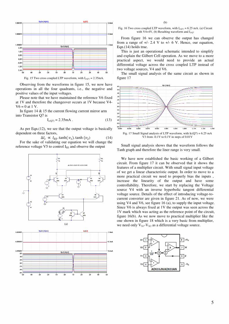
5
Fig. 15 Two cross coupled LTP waveform, with Ic(Q7) = 2.35mA.
Observing from the waveforms in figure 15, we now have
operations in all the four quadrants, i.e., the negative and
positive values of the input voltages.
Please note that we have maintained the reference V6 fixed
at 1V and therefore the changeover occurs at 1V because V4-
V6 = 0 at 1 V.
In figure 14 & 15 the current flowing current mirror arm
into Transistor Q7 is
Ic(Q7) = 2.35mA . (13)
As per Eqn.(12), we see that the output voltage is basically
dependent on three factors,
∆�� ∝ ��� . tanh( G�). tanh(G�) (14)
For the sake of validating our equation we will change the
reference voltage V5 to control IEE and observe the output
(a)
(b)
Fig. 16 Two cross coupled LTP waveform, with Ic(Q7) = 6.25 mA. (a) Circuit
with V4=4V, (b) Resulting waveform and Ic(Q7
From figure 16 we can observe the output has changed
from a range of +/- 2.4 V to +/- 6 V. Hence, our equation,
Eqn.(14) holds true.
This is just an operational schematic intended to simplify
and explain the Gilbert Cell operation. As we move to a more
practical aspect, we would need to provide an actual
differential voltage across the cross coupled LTP instead of
two voltage sources, V4 and V6.
The small signal analysis of the same circuit as shown in
figure 17
Fig. 17 Small Signal analysis of LTP waveform, with Ic(Q7) = 6.25 mA
V3 from -0.1V to 0.1V in steps of 0.01V
Small signal analysis shows that the waveform follows the
Tanh graph and therefore the liner range is very small.
We have now established the basic working of a Gilbert
circuit. From figure 17 it can be observed that it shows the
features of a multiplier circuit. With small signal input voltage
of we get a linear characteristic output. In order to move to a
more practical circuit we need to properly bias the inputs ,
increase the linearity of the output and have some
controllability. Therefore, we start by replacing the Voltage
source V4 with an inverse hyperbolic tangent differential
voltage source. Details of the effect of introducing voltage-to-
current converter are given in figure 21. As of now, we were
using V4 and V6, see figure 16 (a), to supply the input voltage.
Since V6 is always fixed at 1V the output was seen across the
1V mark which was acting as the reference point of the circuit,
figure 16(b). As we now move to practical multiplier like the
one shown in figure 18 which is a very basic from multiplier,
we need only VX1-VX2 as a differential voltage source.
6
Fig. 18 Low cost analog multiplier AD633, 8-Lead Plastic DIP (N) Package
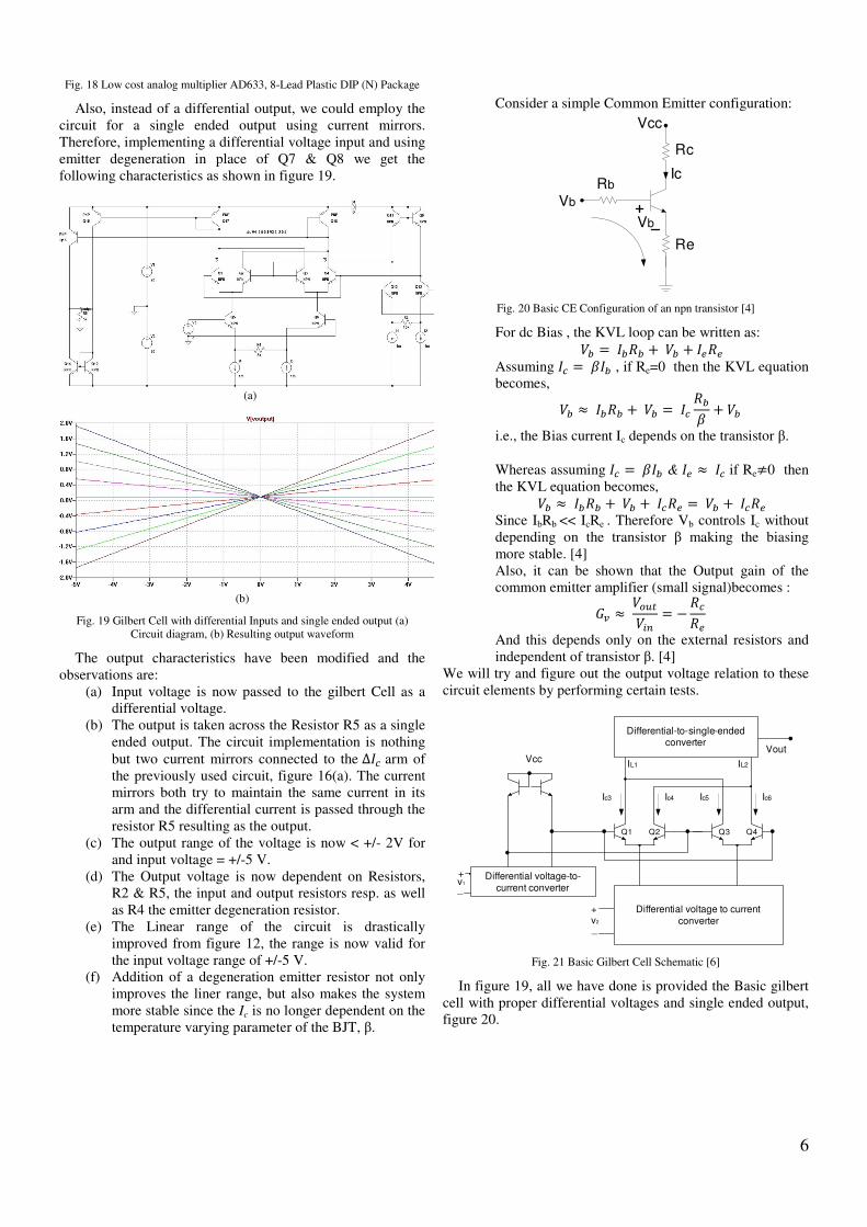
Also, instead of a differential output, we could employ the
circuit for a single ended output using current mirrors.
Therefore, implementing a differential voltage input and using
emitter degeneration in place of Q7 & Q8 we get the
following characteristics as shown in figure 19.
(a)
(b)
Fig. 19 Gilbert Cell with differential Inputs and single ended output (a)
Circuit diagram, (b) Resulting output waveform
The output characteristics have been modified and the
observations are:
(a) Input voltage is now passed to the gilbert Cell as a
differential voltage.
(b) The output is taken across the Resistor R5 as a single
ended output. The circuit implementation is nothing
but two current mirrors connected to the ∆�� arm of
the previously used circuit, figure 16(a). The current
mirrors both try to maintain the same current in its
arm and the differential current is passed through the
resistor R5 resulting as the output.
(c) The output range of the voltage is now < +/- 2V for
and input voltage = +/-5 V.
(d) The Output voltage is now dependent on Resistors,
R2 & R5, the input and output resistors resp. as well
as R4 the emitter degeneration resistor.
(e) The Linear range of the circuit is drastically
improved from figure 12, the range is now valid for
the input voltage range of +/-5 V.
(f) Addition of a degeneration emitter resistor not only
improves the liner range, but also makes the system
more stable since the Ic is no longer dependent on the
temperature varying parameter of the BJT, β.
Consider a simple Common Emitter configuration:
Rb
Rc
Re
Vb
Ic
Vcc
Vb
Fig. 20 Basic CE Configuration of an npn transistor [4]
For dc Bias , the KVL loop can be written as:
"H = �HIH +"H + �I
Assuming �� = J�H , if Re=0 then the KVL equation
becomes,
"H / �HIH +"H = �� IHJ + "H
i.e., the Bias current Ic depends on the transistor β.
Whereas assuming �� = J�H & � / �� if ReK0 then
the KVL equation becomes,
"H / �HIH +"H +��I ="H +��I
Since IbRb << IcRe . Therefore Vb controls Ic without
depending on the transistor β making the biasing
more stable. [4]
Also, it can be shown that the Output gain of the
common emitter amplifier (small signal)becomes :
L< /"(MN"#* = −I�I
And this depends only on the external resistors and
independent of transistor β. [4]
We will try and figure out the output voltage relation to these
circuit elements by performing certain tests.
Ic3 Ic4
v1
+
_
Q1 Q2
+
_v2
Ic1
Q4 Q5
Ic5 Ic6
Q3 Q4
Ic2
IL1 IL2
Differential-to-single-ended converter
Differential voltage to current converter
Vout
Differential voltage-to-current converter
Vcc
Fig. 21 Basic Gilbert Cell Schematic [6]
In figure 19, all we have done is provided the Basic gilbert
cell with proper differential voltages and single ended output,
figure 20.
7
(a) The single ended output is nothing but two
current mirrors trying to balance each other and
the differential current flowing through the Load
resistor. Addition of a differential-to-single-
ended converter adds a parameter in the circuit
as
"(MN =∆�� . ' (15)[6]
Where K is dependent on the load resistance and the
voltage controlled current source in the differential-to-single
ended converter.
(b) Since differential voltage-to-current converter
with input V2 is responsible for the tail currents
in the cross coupled LTP, it has an important
role in output where
"(MN ∝ !9�OP (16)
The Ieo current in Eqn.(16) can be seen in our simulated
circuit, figure 19(a), as the degenerated emitter current source
as, I3 & I4
(c) Similarly, the differential voltage-to-current
converter with input V2 is the main input signal
which controls the LTP pair transistors.
Therefore addition of this converter has an effect
on the output as
"(MN ∝ !2�Q�RRPRSTRROUV
(17)
The Imirror current in Eqn.(16) can be seen in our simulated
circuit, figure 19(a), as the degenerated current source as, I1 &
I2. Practically the purpose of this differential voltage-to-
current converter is to introduce an inverse hyperbolic
Tangent voltage to cancel the effect of the Gilbert Cell’s
equation given in Eqn. (12).
v1
+
_
Differential voltage-to-current converter
∆V
I1 I2
Vcc
Fig. 22 Inverse hyperbolic tangent circuit [6]
The differential voltage source produces a current in
addition to the I1 and I2 shown in the figure 21. The currents
are hence given by,
�� = �( +'�"� , and �� = �( −'�"� (18)
Here Io is the current when V1= 0V, and K1 is the factor
introduced by the voltage-to-converter.
Therefore, the differential voltage ∆" is given by,
∆" � "% ln A�( � '�"��X B �"% ln A�( � '�"��X B
� "% ln Y�P�Z2!2�P�Z2!2[ (19)
Using, tanh�� � � �� ln Y������[
We have,
∆" � 2"% tanh�� YZ2!2�P [ (20)
Substituting Eqn. 20 in Eqn.12 we get ,
∆�� � ��� tanh A G�2G%B tanh AG�2G%B �D ∆�� � ��� YZ2!2�P [ YZ9!9�OP [ (21)[6]
This makes it linear to the Input voltage rather than
hyperbolic tangential.
Our specification is to meet a specification of +/- 10 V
Output for an Input range of +/-5V with flexibility of
controlling the tail current in the cross connected LTPs.
Using Eqn.15, 16 & 17 to vary the circuit parameters, such
as the input and output resistances; the tail current settings;
and the differential voltage V3 controlling the tail currents of
cross coupled LTP in figure 18 is modified to get the desired
output.
(a)
(b)
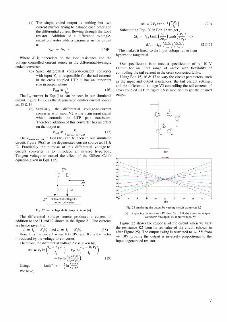
Fig. 23 Analysing the output by varying circuit parameter R2
(a) Replacing the resistance R2 from 5k to 10k (b) Resulting output
waveform V(output) vs. Input voltage, V4
Figure 22 shows the response of the circuit when we vary
the resistance R2 from its set value of the circuit (shown in
after Figure 25). The output swing is restricted to +/- 5V from
+/- 10V proving the output is inversely proportional to the
input degenerated resistor.
8
(a)
(b)
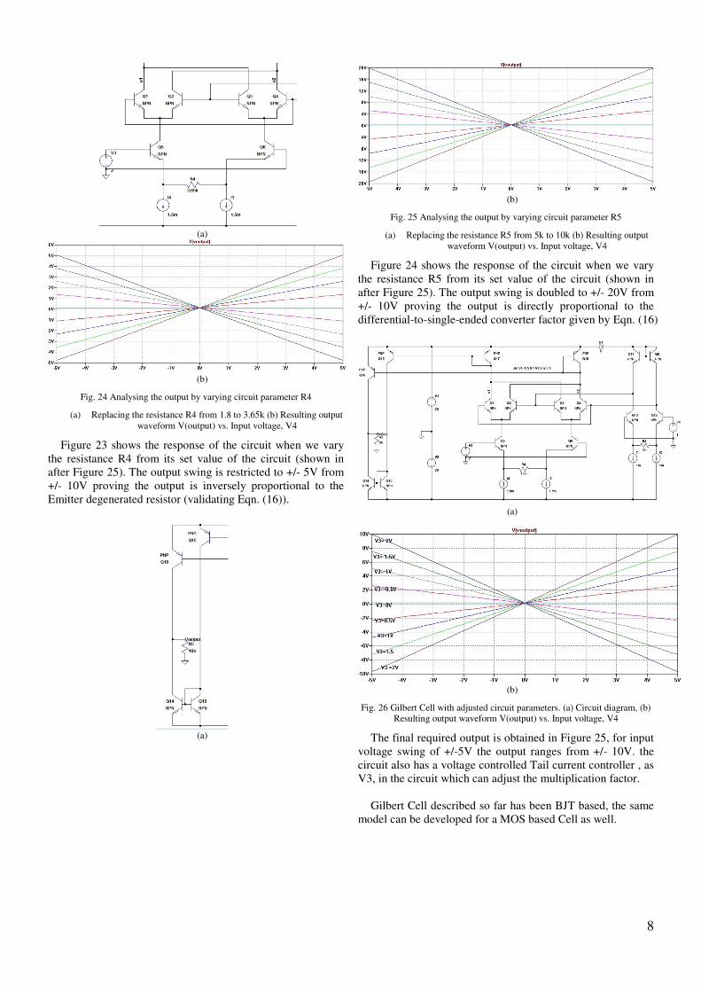
Fig. 24 Analysing the output by varying circuit parameter R4
(a) Replacing the resistance R4 from 1.8 to 3.65k (b) Resulting output
waveform V(output) vs. Input voltage, V4
Figure 23 shows the response of the circuit when we vary
the resistance R4 from its set value of the circuit (shown in
after Figure 25). The output swing is restricted to +/- 5V from
+/- 10V proving the output is inversely proportional to the
Emitter degenerated resistor (validating Eqn. (16)).
(a)
(b)
Fig. 25 Analysing the output by varying circuit parameter R5
(a) Replacing the resistance R5 from 5k to 10k (b) Resulting output
waveform V(output) vs. Input voltage, V4
Figure 24 shows the response of the circuit when we vary
the resistance R5 from its set value of the circuit (shown in
after Figure 25). The output swing is doubled to +/- 20V from
+/- 10V proving the output is directly proportional to the
differential-to-single-ended converter factor given by Eqn. (16)
(a)
(b)
Fig. 26 Gilbert Cell with adjusted circuit parameters. (a) Circuit diagram, (b)
Resulting output waveform V(output) vs. Input voltage, V4
The final required output is obtained in Figure 25, for input
voltage swing of +/-5V the output ranges from +/- 10V. the
circuit also has a voltage controlled Tail current controller , as
V3, in the circuit which can adjust the multiplication factor.
Gilbert Cell described so far has been BJT based, the same
model can be developed for a MOS based Cell as well.
9
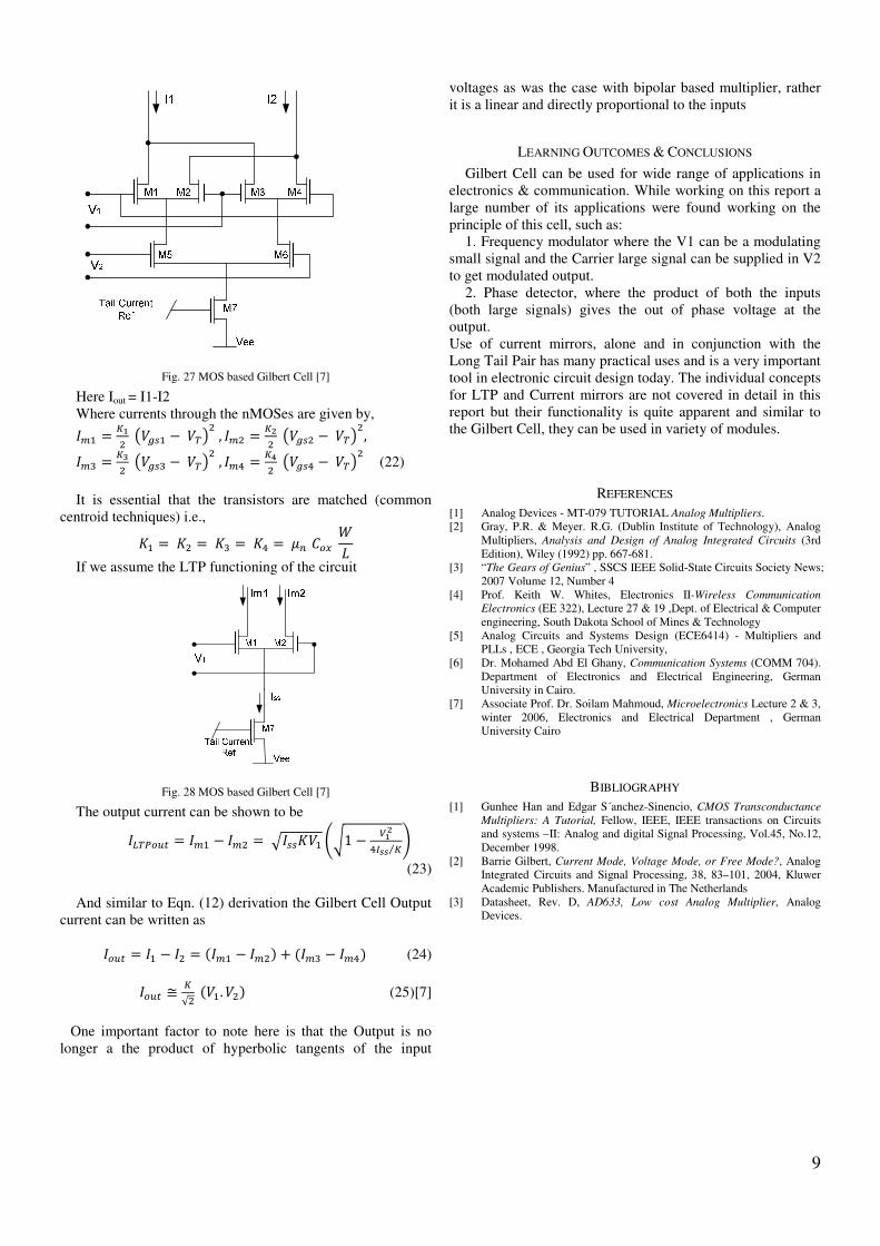
Fig. 27 MOS based Gilbert Cell [7]
Here Iout = I1-I2
Where currents through the nMOSes are given by,
�\� � Z2� ]"̂ X� �"%_�, �\� � Z9
� ]"̂ X� �"%_�, �\0 � Z`
� ]"̂ X0 �"%_�, �\4 � Za� ]"̂ X4 �"%_� (22)
It is essential that the transistors are matched (common
centroid techniques) i.e.,
'� �'� �'0 �'4 �b*c(� de
If we assume the LTP functioning of the circuit
Fig. 28 MOS based Gilbert Cell [7]
The output current can be shown to be
�?%f(MN � �\� � �\� �g�XX'"� hi1 � !294�jj Z⁄ k
(23)
And similar to Eqn. (12) derivation the Gilbert Cell Output
current can be written as
�(MN � �� � �� � ��\� � �\�� � ��\0 � �\4� (24)
�(MN ≅ Z√� �"�. "�� (25)[7]
One important factor to note here is that the Output is no
longer a the product of hyperbolic tangents of the input
voltages as was the case with bipolar based multiplier, rather
it is a linear and directly proportional to the inputs
LEARNING OUTCOMES & CONCLUSIONS
Gilbert Cell can be used for wide range of applications in
electronics & communication. While working on this report a
large number of its applications were found working on the
principle of this cell, such as:
1. Frequency modulator where the V1 can be a modulating
small signal and the Carrier large signal can be supplied in V2
to get modulated output.
2. Phase detector, where the product of both the inputs
(both large signals) gives the out of phase voltage at the
output.
Use of current mirrors, alone and in conjunction with the
Long Tail Pair has many practical uses and is a very important
tool in electronic circuit design today. The individual concepts
for LTP and Current mirrors are not covered in detail in this
report but their functionality is quite apparent and similar to
the Gilbert Cell, they can be used in variety of modules.
REFERENCES
[1] Analog Devices - MT-079 TUTORIAL Analog Multipliers.
[2] Gray, P.R. & Meyer. R.G. (Dublin Institute of Technology), Analog
Multipliers, Analysis and Design of Analog Integrated Circuits (3rd
Edition), Wiley (1992) pp. 667-681.
[3] “The Gears of Genius” , SSCS IEEE Solid-State Circuits Society News;
2007 Volume 12, Number 4
[4] Prof. Keith W. Whites, Electronics II-Wireless Communication
Electronics (EE 322), Lecture 27 & 19 ,Dept. of Electrical & Computer
engineering, South Dakota School of Mines & Technology
[5] Analog Circuits and Systems Design (ECE6414) - Multipliers and
PLLs , ECE , Georgia Tech University,
[6] Dr. Mohamed Abd El Ghany, Communication Systems (COMM 704).
Department of Electronics and Electrical Engineering, German
University in Cairo.
[7] Associate Prof. Dr. Soilam Mahmoud, Microelectronics Lecture 2 & 3,
winter 2006, Electronics and Electrical Department , German
University Cairo
BIBLIOGRAPHY
[1] Gunhee Han and Edgar S´anchez-Sinencio, CMOS Transconductance
Multipliers: A Tutorial, Fellow, IEEE, IEEE transactions on Circuits
and systems –II: Analog and digital Signal Processing, Vol.45, No.12,
December 1998.
[2] Barrie Gilbert, Current Mode, Voltage Mode, or Free Mode?, Analog
Integrated Circuits and Signal Processing, 38, 83–101, 2004, Kluwer
Academic Publishers. Manufactured in The Netherlands
[3] Datasheet, Rev. D, AD633, Low cost Analog Multiplier, Analog
Devices.