Embed Size (px)
Citation preview

Binghamton University Binghamton University
The Open Repository @ Binghamton (The ORB) The Open Repository @ Binghamton (The ORB)
Graduate Dissertations and Theses Dissertations, Theses and Capstones
2017
Design of Experiment Analysis of an Electronics Package Lid Design of Experiment Analysis of an Electronics Package Lid
Using Finite Element Analysis Using Finite Element Analysis
Nupur Bajad Binghamton University--SUNY, [email protected]
Follow this and additional works at: https://orb.binghamton.edu/dissertation_and_theses
Part of the Engineering Commons
Recommended Citation Recommended Citation Bajad, Nupur, "Design of Experiment Analysis of an Electronics Package Lid Using Finite Element Analysis" (2017). Graduate Dissertations and Theses. 53. https://orb.binghamton.edu/dissertation_and_theses/53
This Thesis is brought to you for free and open access by the Dissertations, Theses and Capstones at The Open Repository @ Binghamton (The ORB). It has been accepted for inclusion in Graduate Dissertations and Theses by an authorized administrator of The Open Repository @ Binghamton (The ORB). For more information, please contact [email protected].
DESIGN OF EXPERIMENT ANALYSIS OF AN ELECTRONICS PACKAGE
LID USING FINITE ELEMENT ANALYSIS
BY
NUPUR BAJAD
BE, PUNE UNIVERSITY, 2012
MS, BINGHAMTON UNIVERSITY, 2017
THESIS
Submitted in partial fulfillment of the requirements for
The degree of Master of Science in Industrial & Systems Engineering
in the Graduate School of
Binghamton University
State University of New York
2017

© Copyright by Nupur Bajad 2017
All Rights Reserved
iii
Accepted in partial fulfillment of the requirements for
The degree of Master of Science in Industrial & Systems Engineering
in the Graduate School of Binghamton University
State University of New York
2017
November 28, 2017
Dr. Daryl Santos, Faculty Advisor
Department of Systems Science and Industrial Engineering,
Binghamton University
Dr. Sang Won Yoon, Committee Member
Department of Systems Science and Industrial Engineering,
Binghamton University
Mr. David Bolognia, Committee Member
Senior Package Development Manager, Systems in Package group at
Analog Devices, Inc. Wilmington MA
iv
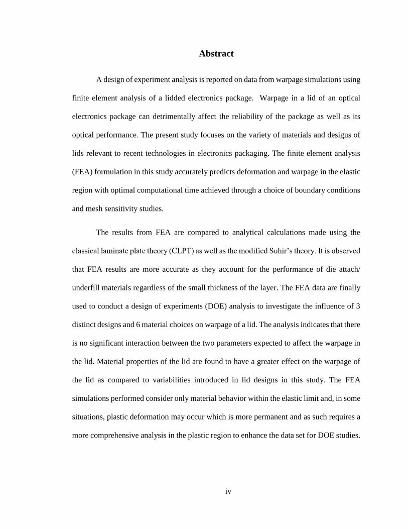
Abstract
A design of experiment analysis is reported on data from warpage simulations using
finite element analysis of a lidded electronics package. Warpage in a lid of an optical
electronics package can detrimentally affect the reliability of the package as well as its
optical performance. The present study focuses on the variety of materials and designs of
lids relevant to recent technologies in electronics packaging. The finite element analysis
(FEA) formulation in this study accurately predicts deformation and warpage in the elastic
region with optimal computational time achieved through a choice of boundary conditions
and mesh sensitivity studies.
The results from FEA are compared to analytical calculations made using the
classical laminate plate theory (CLPT) as well as the modified Suhir’s theory. It is observed
that FEA results are more accurate as they account for the performance of die attach/
underfill materials regardless of the small thickness of the layer. The FEA data are finally
used to conduct a design of experiments (DOE) analysis to investigate the influence of 3
distinct designs and 6 material choices on warpage of a lid. The analysis indicates that there
is no significant interaction between the two parameters expected to affect the warpage in
the lid. Material properties of the lid are found to have a greater effect on the warpage of
the lid as compared to variabilities introduced in lid designs in this study. The FEA
simulations performed consider only material behavior within the elastic limit and, in some
situations, plastic deformation may occur which is more permanent and as such requires a
more comprehensive analysis in the plastic region to enhance the data set for DOE studies.
v
Acknowledgements
I am grateful to State University of New York at Binghamton and faculty for giving
me this wonderful opportunity. I would first like to thank my research advisor Dr. Daryl
Santos. He allowed this research to be my own work but guided me in the right direction
whenever I needed. I would to thank Dr. Srihari, Dr. Khasawneh, and Mr. Havens for
unfailing support and assistance for research. I would like to thank Ms. M Giorgio for
providing emotional support and care when I was in Binghamton. I would also like to thank
Analog Devices, Inc., for providing fantastic opportunity to conduct most of my research
in your facility. Particularly, I am grateful to Mr. Tom Goida, Mr. David Bolognia, and Dr.
Venkatadri for valuable mentoring, insightful conversations and timely advice.
I am grateful to my parents and my brother Anurag, for providing emotional as well
as moral support through my entire journey of pursuing Master’s degree. A special thanks
to my partner in life, Aniket for filling me up with all the good food and cheering me up.
Also, I am grateful to my extended family and friends for support.
Thank you all for your encouragement!
vi
Table of Contents
List of Tables .................................................................................................................... vii
List of Figures .................................................................................................................. viii
1. Introduction ................................................................................................................. 1
1.1. Overview .............................................................................................................. 1
1.2. Techniques available to measure the warpage ..................................................... 2
1.3. Research Objective ............................................................................................... 6
1.4. Significance of research ....................................................................................... 9
2. Literature Review ...................................................................................................... 11
2.1. Experimental Methods ....................................................................................... 11
2.1.1. Gauge-Indicator Shim method .................................................................... 12
2.1.2. Contact profilometry ................................................................................... 12
2.1.3. Non-contact profilometry............................................................................ 14
2.1.4. Optical interferometry ................................................................................. 14
2.1.5. Moiré Methods ............................................................................................ 15
2.2. Analytical and numerical methods ..................................................................... 17
2.2.1. FEA Analysis- Numerical method .............................................................. 17
2.2.2. Analytical method- Classical laminate plate theory (CLPT) ...................... 20
2.2.3. Modified Suhir’s solution ........................................................................... 24
2.3. Summary ............................................................................................................ 26
3. Research Methodology ............................................................................................. 28
3.1. Research Experiment – Case study .................................................................... 28
3.2. Plan of experimentation process for DOE.......................................................... 33
3.3. Summary ............................................................................................................ 40
4. Results and Discussion ............................................................................................. 41
4.1. Comparison of results for analytical methods and FEA method ....................... 41
4.2. Design of experiment analysis ........................................................................... 44
4.3. Summary ............................................................................................................ 49
5. Conclusions and Future Work .................................................................................. 51
6. References Cited ....................................................................................................... 54
vii
List of Tables
Table 2.1: Comparison of the different techniques available for measuring warpage based
on measurement features................................................................................................... 16
Table 3.1: Dimensional details and Material properties of different layers in LGA package
........................................................................................................................................... 29
Table 3.2: Dimensional details and Material properties of different layers in package used
for experiment ................................................................................................................... 34
Table 3.3: Material properties considered for lid.............................................................. 38
Table 3.4: DOE matrix based on parameters .................................................................... 38
Table 4.1: DOE matrix obtained by parametric study in simulation ................................ 44
viii
List of Figures
Figure 1.1: Convex (+) warpage ......................................................................................... 1
Figure 1.2: Concave (-) warpage ........................................................................................ 2
Figure 1.3: (a) Digital image correlation setup, (b) Triangulation setup ............................ 4
Figure 1.4: Experimental setup for the Shadow Moiré method .......................................... 5
Figure 1.5: Schematic of focus of research area ................................................................. 7
Figure 1.6: Commercially available CO2 Sensor which uses lid as gas cavity. ................. 9
Figure 2.1: Filler gauge set... ............................................................................................ 12
Figure 2.2: Schematic of stylus profilometer .................................................................... 13
Figure 2.3: Optical configuration of the Fizeau Interferometry ....................................... 15
Figure 2.4: Graphical representation of the comparison table 2.1 .................................... 17
Figure 2.5: Basic mapping of modeling and simulation in semiconductor industry ........ 18
Figure 2.6: Flowchart for FEA method processing .......................................................... 19
Figure 2.7: Geometry of laminate considering ‘N’ layers ................................................ 20
Figure 2.8: Geometry of Package highlighting the overhang ........................................... 22
Figure 2.9: Geometry of Package highlighting the layer where effective material properties
are to be considered .......................................................................................................... 24
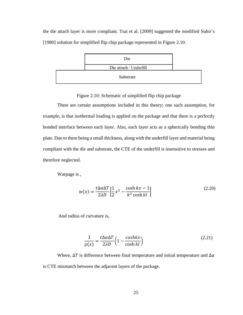
Figure 2.10: Schematic of simplified flip chip package ................................................... 25
Figure 3.1: Front view of the cross section of quarter model of LGA showing layers
categorized in different colors .......................................................................................... 29
Figure 3.2: Quarter FEA meshed model of LGA ............................................................. 30
Figure 3.3: Quarter FEA model showing deformation contour measured in µm on LGA at
25°C .................................................................................................................................. 31
Figure 3.4: Quarter FEA model showing deformation contour measured in µm on LGA at
260°C ................................................................................................................................ 31
Figure 3.5: Construction Path along center to diagonally opposite vertex in which is useful
to measure warpage of the package .................................................................................. 32
Figure 3.6: Warpage curve along half diagonal of LGA in simulation ............................ 33
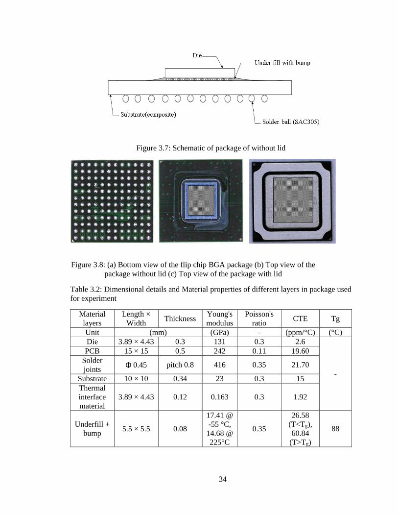
Figure 3.7: Schematic of package of without lid .............................................................. 34
Figure 3.8: (a) Bottom view of the flip chip BGA package (b) Top view of the package
without lid (c) Top view of the package with lid .............................................................. 34
Figure 3.9: Cross section of the lidded package without PCB shows composite layer of
underfill- micro bumps and substrate ............................................................................... 35
Figure 3.10: Front view of cross section of 3D model of package used in experiment .... 36
ix
Figure 3.11: Meshed model of the package ...................................................................... 36
Figure 3.12: Deformation measured in µm for mesh sensitivity study ............................ 36
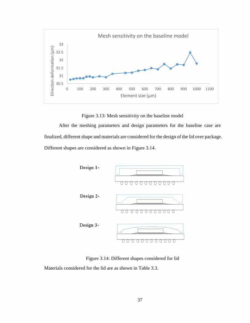
Figure 3.13: Mesh sensitivity on the baseline model ........................................................ 37
Figure 3.14: Different shapes considered for lid .............................................................. 37
Figure 3.15: Research methodology of the experiment .................................................... 39
Figure 4.1: Isometric view of meshed quarter model of package considering there layers
before solder and reflowing process ................................................................................. 42
Figure 4.2: Warpage measured in µm along the mid plane of the package in X-direction
........................................................................................................................................... 42
Figure 4.3: Comparison of the Warpage measured by all techniques along the mid plane of
the package in the X-direction .......................................................................................... 44
Figure 4.4: Various plots obtained using ANOVA technique .......................................... 45
Figure 4.5: ANOVA data analysis result .......................................................................... 46
Figure 4.6: Pareto chart highlighting the significance of the material and design parameter
........................................................................................................................................... 48
Figure 4.7: Interaction plot considering all the simulation cases for DOE ....................... 48
Figure 4.8: Main effects plot of the two parameters individually with respect to mean of
response............................................................................................................................. 49
1
1. Introduction
1.1. Overview
Warpage, which is mainly considered as out-of-plane deformation of an electronics
package, is deformation that crucially affects the reliability of the surface mount packages.
During a series of manufacturing processes of the electronic packages, such as printed wire
board fabrication, solder paste printing, solder reflow process, etc., different
thermomechanical stresses are generated in the package. Sometimes these stresses lead to
fatigue and, eventually, cracks in the solder joints or other defects. These stresses can also
lead to warpage of the package which, as noted above, can adversely affect reliability in
terms of leading to solder joint defects as well as die cracking and delamination.
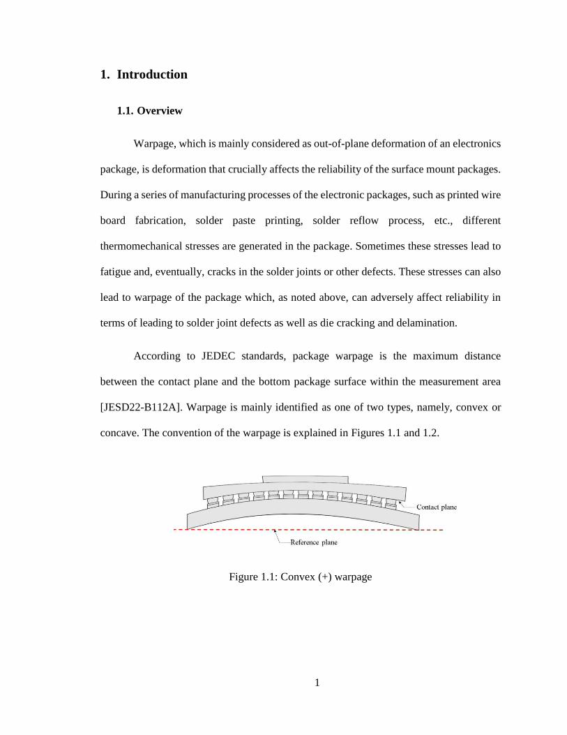
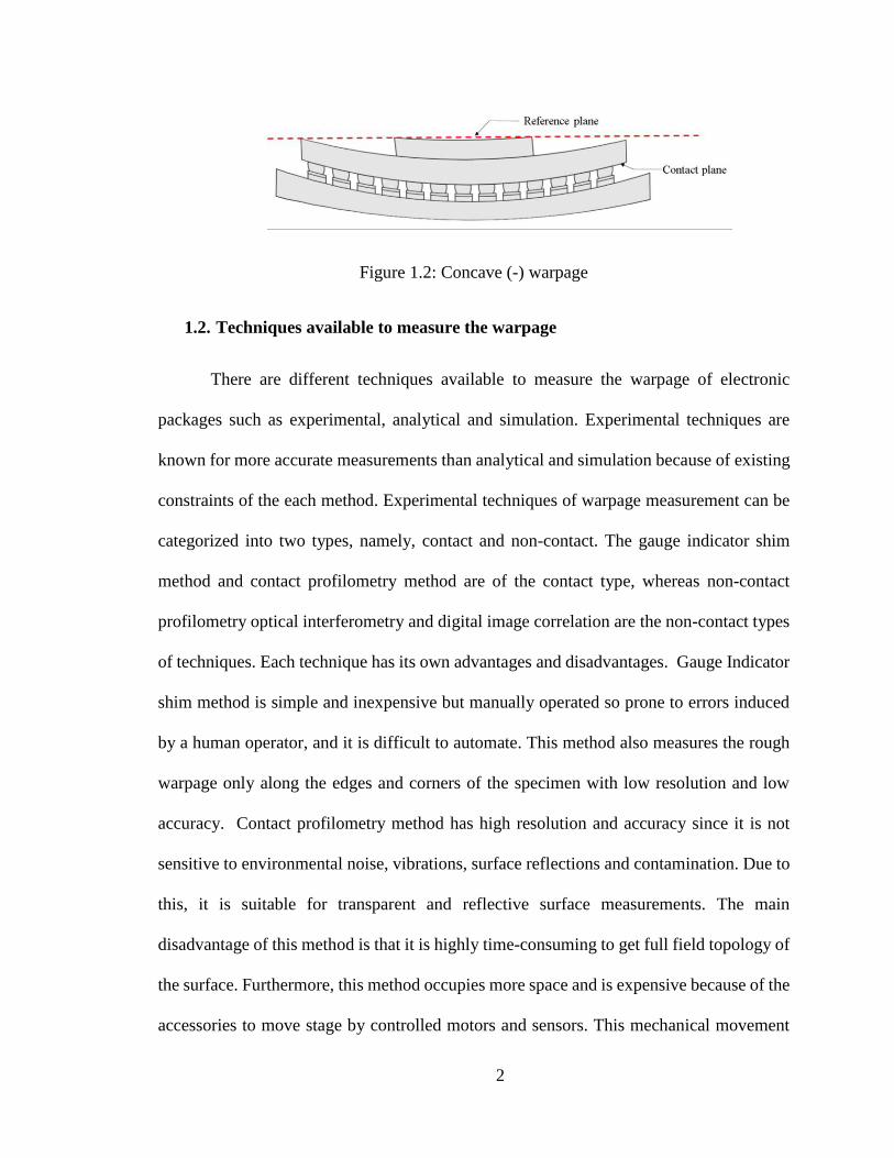
According to JEDEC standards, package warpage is the maximum distance
between the contact plane and the bottom package surface within the measurement area
[JESD22-B112A]. Warpage is mainly identified as one of two types, namely, convex or
concave. The convention of the warpage is explained in Figures 1.1 and 1.2.
Figure 1.1: Convex (+) warpage
2
Figure 1.2: Concave (-) warpage
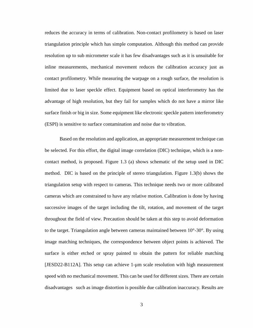
1.2. Techniques available to measure the warpage
There are different techniques available to measure the warpage of electronic
packages such as experimental, analytical and simulation. Experimental techniques are
known for more accurate measurements than analytical and simulation because of existing
constraints of the each method. Experimental techniques of warpage measurement can be
categorized into two types, namely, contact and non-contact. The gauge indicator shim
method and contact profilometry method are of the contact type, whereas non-contact
profilometry optical interferometry and digital image correlation are the non-contact types
of techniques. Each technique has its own advantages and disadvantages. Gauge Indicator
shim method is simple and inexpensive but manually operated so prone to errors induced
by a human operator, and it is difficult to automate. This method also measures the rough
warpage only along the edges and corners of the specimen with low resolution and low
accuracy. Contact profilometry method has high resolution and accuracy since it is not
sensitive to environmental noise, vibrations, surface reflections and contamination. Due to
this, it is suitable for transparent and reflective surface measurements. The main
disadvantage of this method is that it is highly time-consuming to get full field topology of
the surface. Furthermore, this method occupies more space and is expensive because of the
accessories to move stage by controlled motors and sensors. This mechanical movement
3
reduces the accuracy in terms of calibration. Non-contact profilometry is based on laser
triangulation principle which has simple computation. Although this method can provide
resolution up to sub micrometer scale it has few disadvantages such as it is unsuitable for
inline measurements, mechanical movement reduces the calibration accuracy just as
contact profilometry. While measuring the warpage on a rough surface, the resolution is
limited due to laser speckle effect. Equipment based on optical interferometry has the
advantage of high resolution, but they fail for samples which do not have a mirror like
surface finish or big in size. Some equipment like electronic speckle pattern interferometry
(ESPI) is sensitive to surface contamination and noise due to vibration.
Based on the resolution and application, an appropriate measurement technique can
be selected. For this effort, the digital image correlation (DIC) technique, which is a non-
contact method, is proposed. Figure 1.3 (a) shows schematic of the setup used in DIC
method. DIC is based on the principle of stereo triangulation. Figure 1.3(b) shows the
triangulation setup with respect to cameras. This technique needs two or more calibrated
cameras which are constrained to have any relative motion. Calibration is done by having
successive images of the target including the tilt, rotation, and movement of the target
throughout the field of view. Precaution should be taken at this step to avoid deformation
to the target. Triangulation angle between cameras maintained between 10°-30°. By using
image matching techniques, the correspondence between object points is achieved. The
surface is either etched or spray painted to obtain the pattern for reliable matching
[JESD22-B112A]. This setup can achieve 1-µm scale resolution with high measurement
speed with no mechanical movement. This can be used for different sizes. There are certain
disadvantages such as image distortion is possible due calibration inaccuracy. Results are
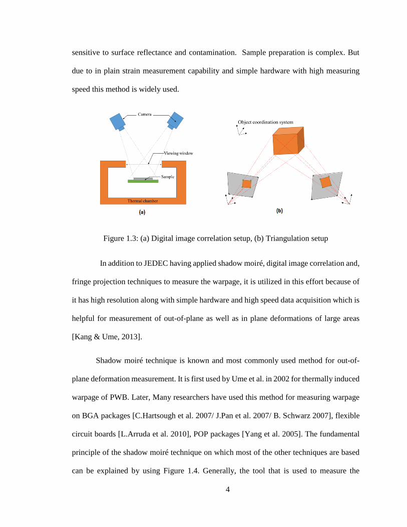
4
sensitive to surface reflectance and contamination. Sample preparation is complex. But
due to in plain strain measurement capability and simple hardware with high measuring
speed this method is widely used.
Figure 1.3: (a) Digital image correlation setup, (b) Triangulation setup
In addition to JEDEC having applied shadow moiré, digital image correlation and,
fringe projection techniques to measure the warpage, it is utilized in this effort because of
it has high resolution along with simple hardware and high speed data acquisition which is
helpful for measurement of out-of-plane as well as in plane deformations of large areas
[Kang & Ume, 2013].
Shadow moiré technique is known and most commonly used method for out-of-
plane deformation measurement. It is first used by Ume et al. in 2002 for thermally induced
warpage of PWB. Later, Many researchers have used this method for measuring warpage
on BGA packages [C.Hartsough et al. 2007/ J.Pan et al. 2007/ B. Schwarz 2007], flexible
circuit boards [L.Arruda et al. 2010], POP packages [Yang et al. 2005]. The fundamental
principle of the shadow moiré technique on which most of the other techniques are based
can be explained by using Figure 1.4. Generally, the tool that is used to measure the
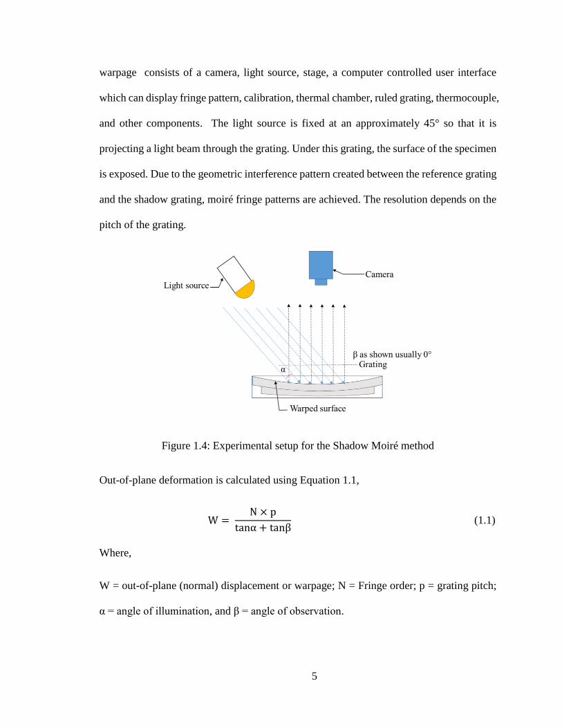
5
warpage consists of a camera, light source, stage, a computer controlled user interface
which can display fringe pattern, calibration, thermal chamber, ruled grating, thermocouple,
and other components. The light source is fixed at an approximately 45° so that it is
projecting a light beam through the grating. Under this grating, the surface of the specimen
is exposed. Due to the geometric interference pattern created between the reference grating
and the shadow grating, moiré fringe patterns are achieved. The resolution depends on the
pitch of the grating.
Figure 1.4: Experimental setup for the Shadow Moiré method
Out-of-plane deformation is calculated using Equation 1.1,
W = N × p
tanα + tanβ (1.1)
Where,
W = out-of-plane (normal) displacement or warpage; N = Fringe order; p = grating pitch;
α = angle of illumination, and β = angle of observation.
6
Shadow moiré method has proven most suitable by Yeh et al. in the year 1991 since
it is easy to use and less expensive, the ability for full field measurement, but during the
analysis, the glass grating is located very near to the surface of the sample. This may affect
the thermal behavior of the sample. Mechanical moving is another issue in this method
where calibration accuracy is decreased. If the sample has shiny surfaces then usually it is
painted in a white color to produce fringe.
Along with the experimental measuring tools, other methods can help to measure
the deformation that is known as analytical techniques. For example, an analytical model
that uses classical laminate plate theory (CLPT) is also utilized in the electronics packaging
community. Herein, the package is considered as a composite with ‘N’ number of layers,
comprised of different materials, and the technique considers the temperature dependent
properties of the different materials. Simplified assumptions based on kinematic
constraints are applied to multi-layered laminates to provide the thermo-mechanically
produced displacement field at the mid-plane which essentially is considered as warpage
[Park et al. 2007]. Furthermore, there is a large body of work that incorporates finite
element analysis (FEA) to deduce warpage [Ke et al. 2009/ Jang et al. 2012 /Xiong et al.
2009]. In this method, which is simulation-based, a prototype is generated with a
resemblance to the actual product and deformation is measured/estimated when subjected
to a simulated thermomechanical load.
1.3. Research Objective
The research objective of this work is to develop a DOE analytical method focusing
on improving the performance of an electronic package lid. A sub-objective of this work
is to try to understand the effect of material and design shape on warpage of the lid by
7
performing parametric analysis. This is important for technically advanced packages as
shown in Figure 1.6 where purpose of the lid is not only protection and separation of the
system boundary from surrounding but also provide cavity to hold the gas and optical path.
In such cases, small amount of warpage in lid may cause failure to entire package.
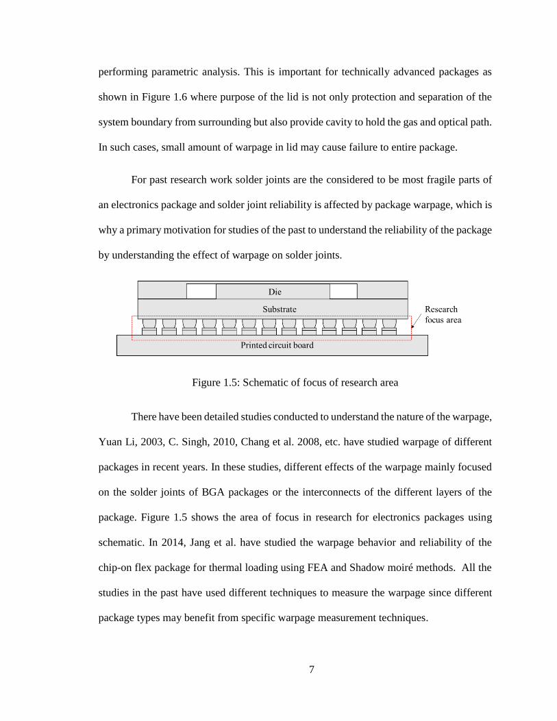
For past research work solder joints are the considered to be most fragile parts of
an electronics package and solder joint reliability is affected by package warpage, which is
why a primary motivation for studies of the past to understand the reliability of the package
by understanding the effect of warpage on solder joints.
Figure 1.5: Schematic of focus of research area
There have been detailed studies conducted to understand the nature of the warpage,
Yuan Li, 2003, C. Singh, 2010, Chang et al. 2008, etc. have studied warpage of different
packages in recent years. In these studies, different effects of the warpage mainly focused
on the solder joints of BGA packages or the interconnects of the different layers of the
package. Figure 1.5 shows the area of focus in research for electronics packages using
schematic. In 2014, Jang et al. have studied the warpage behavior and reliability of the
chip-on flex package for thermal loading using FEA and Shadow moiré methods. All the
studies in the past have used different techniques to measure the warpage since different
package types may benefit from specific warpage measurement techniques.
8
Although experimental methods provide more realistic measurements of the
deformation/warpage, they may have constraints of expensive hardware, limitation over
skills to operate, calibration accuracy, possibility to introduce human error. Similarly, finite
element analysis method has the advantage of creating a prototype and solve under
different loading conditions with less time but validation of the method is necessary and
skills to operate software along with the cost to use this commercially available software.
An analytical method has limitations for providing a suitable solution for all types and
designs of the package. The analytical method also focuses more on estimating warpage
on the mid plane of the package where as in simulation focus of the study can be associated
with different components of the package.
There is a wide variety of materials utilized in electronics packagings such as
metals, plastics, liquid crystal polymers (LCP), and others. Depending on the application,
packaging materials need to be wisely selected. For example, the shrinkage phenomenon
is a concern for plastic materials and, thus, warpage can be a major concern. Shrinkage
occurs due to the polymer varying its density when there is a change in the temperature.
During injection molding, variation in the shrinkage creates residual stresses. These
residual stresses play an important role in the warpage of the part since warpage occurs
where the product does not follow the intended design. So, ideally, if the shrinkage is
uniform throughout the part then the part may not warp. But, due to the interaction of many
factors such as molecular orientations, mold cooling temperature, the design of parts, etc.,
it is difficult to achieve uniform shrinkage [Fischer J. 2013].
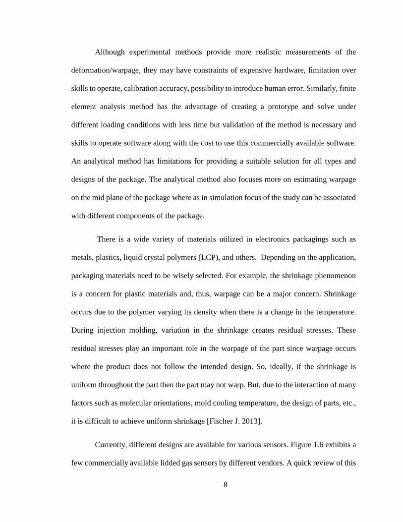
Currently, different designs are available for various sensors. Figure 1.6 exhibits a
few commercially available lidded gas sensors by different vendors. A quick review of this
9
figure suggests that different designs of lids are considered, and the purpose of the lid is
not limited to providing protection during or post-assembly.
Figure 1.6: Commercially available CO2 Sensor which uses lid as gas cavity
Two sensors shown on the left and right are different CO2 sensor modules made by SOHA
Tech Co.,Ltd [Retrieved from: http://sensor-co2.com/products/co2-module/?ckattempt=1]
1.4. Significance of research
This research mainly focuses on how warpage is affecting the lid deformation and
techniques to characterize it. As discussed earlier, FEA tool is used in this study to create
a prototype which is similar to the actual product. The experiment is designed considering
different variables such as the design of the lid and the material of the lid. Methods of the
design of experiment analysis are applied to understand the correlation between these
parameters. The most significant parameter in terms of the warpage deformation is
addressed. Based on this study the appropriate design and material are suggested for the
development of the lid over the package. This becomes helpful when there is an
optoelectronic package undergoing thermomechanical loading; warpage may not only

10
adversely affect solder joints but other parts of the package as well. So in this research
work, characterization of the lid of the package affected by warpage is the focus area. This
study will be helpful for the development of the technologically advanced packages
associated with optoelectronics.
11
2. Literature Review
As briefly discussed in Chapter 1, there are different methods to estimate the out-
of-plane deformation when a package is subjected to thermomechanical loading conditions.
These methods can be analytical, numerical or experimental. With respect to analytical
techniques, Suhir’s theory [1980] for analytical warpage prediction for die – substrate
assembly and classical laminate plate theory (CLPT) by S.B. Park [2007] are well known.
Finite element analysis (FEA) is an automated technique that can be used to estimate the
deformation based on numerical calculations.
More details on the development of experimental methods are presented in Section
2.1 and those of some analytical methods are discussed in Section 2.2.
2.1. Experimental Methods
As mentioned in Chapter 1 experimental methods are classified into contact as well
as non-contact type. The following are some of the experimental methods utilized in the
electronics industry to estimate warpage.
12
2.1.1. Gauge-Indicator Shim method
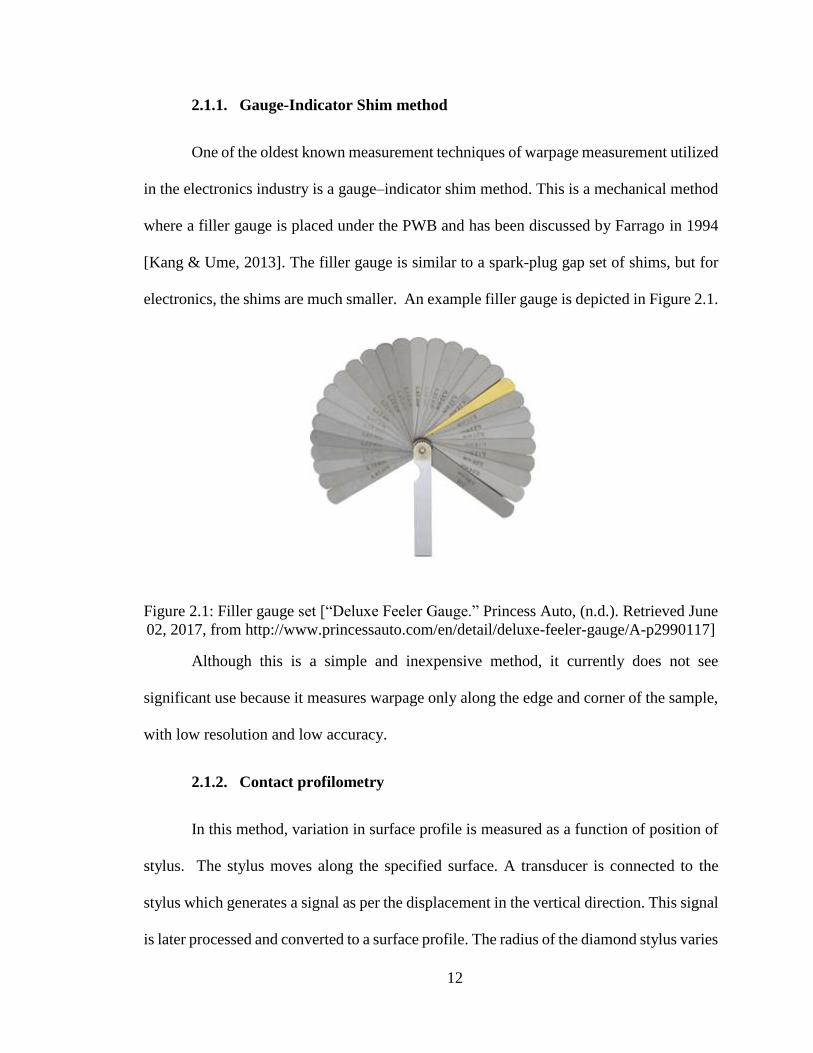
One of the oldest known measurement techniques of warpage measurement utilized
in the electronics industry is a gauge–indicator shim method. This is a mechanical method
where a filler gauge is placed under the PWB and has been discussed by Farrago in 1994
[Kang & Ume, 2013]. The filler gauge is similar to a spark-plug gap set of shims, but for
electronics, the shims are much smaller. An example filler gauge is depicted in Figure 2.1.
Figure 2.1: Filler gauge set [“Deluxe Feeler Gauge.” Princess Auto, (n.d.). Retrieved June
02, 2017, from http://www.princessauto.com/en/detail/deluxe-feeler-gauge/A-p2990117]
Although this is a simple and inexpensive method, it currently does not see
significant use because it measures warpage only along the edge and corner of the sample,
with low resolution and low accuracy.
2.1.2. Contact profilometry
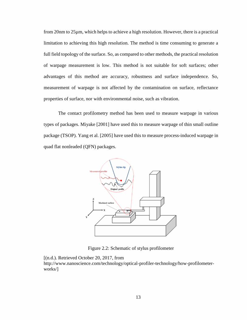
In this method, variation in surface profile is measured as a function of position of
stylus. The stylus moves along the specified surface. A transducer is connected to the
stylus which generates a signal as per the displacement in the vertical direction. This signal
is later processed and converted to a surface profile. The radius of the diamond stylus varies
13
from 20nm to 25µm, which helps to achieve a high resolution. However, there is a practical
limitation to achieving this high resolution. The method is time consuming to generate a
full field topology of the surface. So, as compared to other methods, the practical resolution
of warpage measurement is low. This method is not suitable for soft surfaces; other
advantages of this method are accuracy, robustness and surface independence. So,
measurement of warpage is not affected by the contamination on surface, reflectance
properties of surface, nor with environmental noise, such as vibration.
The contact profilometry method has been used to measure warpage in various
types of packages. Miyake [2001] have used this to measure warpage of thin small outline
package (TSOP). Yang et al. [2005] have used this to measure process-induced warpage in
quad flat nonleaded (QFN) packages.
Figure 2.2: Schematic of stylus profilometer
[(n.d.). Retrieved October 20, 2017, from
http://www.nanoscience.com/technology/optical-profiler-technology/how-profilometer-
works/]
14
Experimental methods mentioned above are of contact type. In-line measurement
capability for contact type of methods is zero. Some of these non-contact type methods are
as discussed, below.
2.1.3. Non-contact profilometry
This method is also called as optical profilometry because it uses an optical
approach. The reflected light from the specimen is used to generate a 3D surface profile
applying the triangulation principle as shown in Figure 1.3 (b) and discussed in Chapter 1
along with the digital image correlation (DIC) method.
2.1.4. Optical interferometry
This method mainly uses the interference of the light waves for surface diagnostics.
A wide variety of configurations is available in this type for warpage measurement of
electronic packages. A few well-known configurations are Twyman–Green interferometry,
Fizeau interferometry, and Electronic speckle–pattern interferometry. The basic principle
of these methods is the same but there are differences in the optical setup to achieve the
interference patterns. Application of Twyman–Green interferometry is limited since it
requires a mirror-like surface. Also, the measurement sensitivity is within a fraction of a
micron, which is sufficient to resolve the warpage observed in advanced electronic
packages.
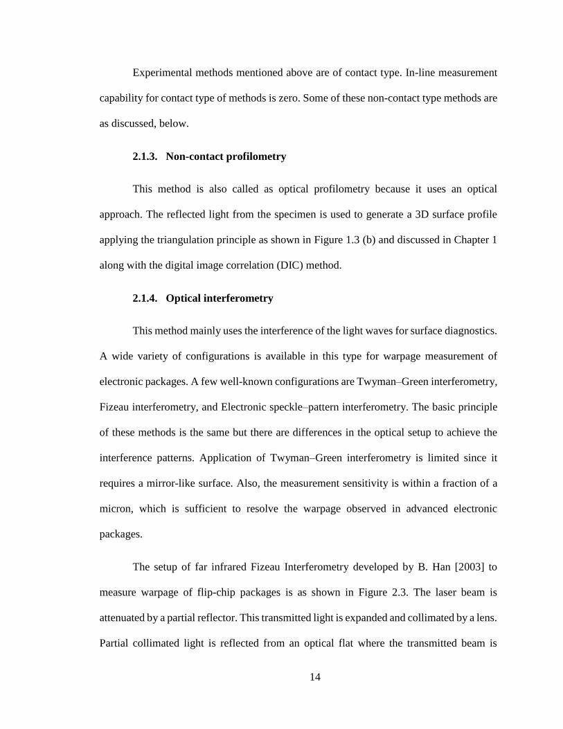
The setup of far infrared Fizeau Interferometry developed by B. Han [2003] to
measure warpage of flip-chip packages is as shown in Figure 2.3. The laser beam is
attenuated by a partial reflector. This transmitted light is expanded and collimated by a lens.
Partial collimated light is reflected from an optical flat where the transmitted beam is
15
reflected from the specimen. Both of these reflected beams are collected by an infrared
camera. This method is mostly used to measure samples of small size and the setup is
complex and expensive.
Figure 2.3: Optical configuration of the Fizeau Interferometry by Han [2003]
2.1.5. Moiré Methods
Moiré methods are widely known/utilized and are based on the fringe projections
that can define the surface topology. The methods were introduced in 1967 by Rowe and
Welford. Moiré fringes are generated by interference of two periodic grating lines, one is
a reference, where the other is the specimen’s grating lines. As the specimen deforms under
load, the specimen grating lines also get distorted. This helps to get surface height variation
experienced by the sample. Based on the location of the specimen grating, this method is
characterized further in two types, namely, in-plane and out-of-plane moiré. In the case of
in-plane moiré, the specimen grating is either attached or printed to the specimen surface
and the reference grating is fixed with constant period and spatial orientation. In the case
of out-of-plane moiré, which is also known as moiré topology, a fringe pattern is developed
16
by superimposing both the gratings. Specimen grating is adjusted and distorted with
reference of out-of-plane displacement (warpage) of the specimen. The out-of-plane moiré
method is more useful to measure warpage of the chip packages and PWB assemblies due
to high resolution and capability to measure large areas.
Based on the different methods to generate and study fringe patterns the moiré
method is classified as Shadow moiré, Projection moiré and Digital fringe projection. This
is because the methods for generation of fringe evolved since successful use of shadow
moiré method by Ume et al. at the Georgia Institute of Technology [2002] for measuring
warpage of printed wire boards (PWB).
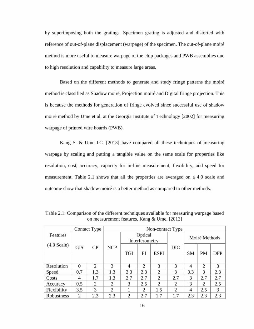
Kang S. & Ume I.C. [2013] have compared all these techniques of measuring
warpage by scaling and putting a tangible value on the same scale for properties like
resolution, cost, accuracy, capacity for in-line measurement, flexibility, and speed for
measurement. Table 2.1 shows that all the properties are averaged on a 4.0 scale and
outcome show that shadow moiré is a better method as compared to other methods.
Table 2.1: Comparison of the different techniques available for measuring warpage based
on measurement features, Kang & Ume. [2013]
Features
(4.0 Scale)
Contact Type Non-contact Type
GIS CP NCP
Optical
Interferometry
DIC
Moiré Methods
TGI FI ESPI SM PM DFP
Resolution 0 2 3 4 2 3 3 4 2 3
Speed 0.7 1.3 1.3 2.3 2.3 2 3 3.3 3 2.3
Costs 4 1.7 1.3 2.7 2.7 2 2.7 3 2.7 2.7
Accuracy 0.5 2 2 3 2.5 2 2 3 2 2.5
Flexibility 3.5 3 2 1 2 1.5 2 4 2.5 3
Robustness 2 2.3 2.3 2 2.7 1.7 1.7 2.3 2.3 2.3
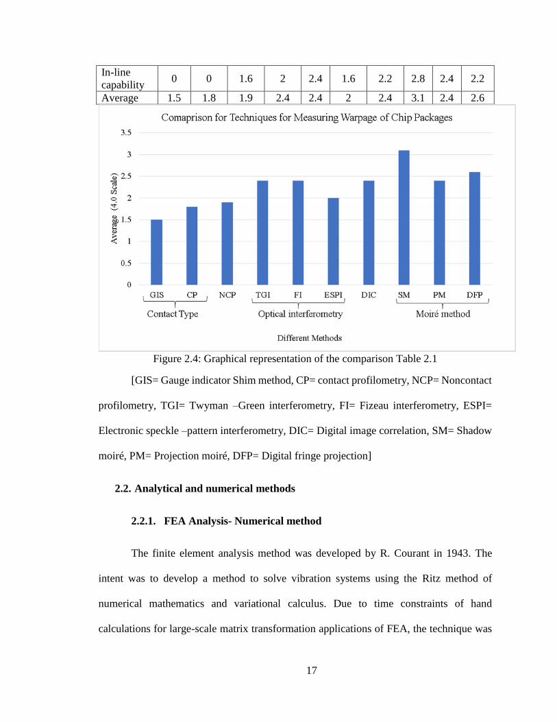
17
In-line
capability 0 0 1.6 2 2.4 1.6 2.2 2.8 2.4 2.2
Average 1.5 1.8 1.9 2.4 2.4 2 2.4 3.1 2.4 2.6
Figure 2.4: Graphical representation of the comparison Table 2.1
[GIS= Gauge indicator Shim method, CP= contact profilometry, NCP= Noncontact
profilometry, TGI= Twyman –Green interferometry, FI= Fizeau interferometry, ESPI=
Electronic speckle –pattern interferometry, DIC= Digital image correlation, SM= Shadow
moiré, PM= Projection moiré, DFP= Digital fringe projection]
2.2. Analytical and numerical methods
2.2.1. FEA Analysis- Numerical method
The finite element analysis method was developed by R. Courant in 1943. The
intent was to develop a method to solve vibration systems using the Ritz method of
numerical mathematics and variational calculus. Due to time constraints of hand
calculations for large-scale matrix transformation applications of FEA, the technique was
18
limited at that time. In early 1970, the FEA method was mainly used for aeronautics as
well as automotive industries as based on the research done by Argyris et al. [1950] in
design of airframe and some basic structural analysis of automobile chassis. Yet due to the
lack of high computation performance and high price of mainframe computers, FEA was
only applied to simple structural analysis. As computing became cheaper, coupled with
increased computational speed, FEA gained tremendous use. Current software packages,
including ANSYS, Flotherm, and others, offer comprehensive multi-physics solutions
while considering different analytical conditions such as structural, thermal, fluid, and
electromagnetic. In the area of electronics packaging, thermo-mechanical loading
conditions play an essential role to define the reliability of the packages.
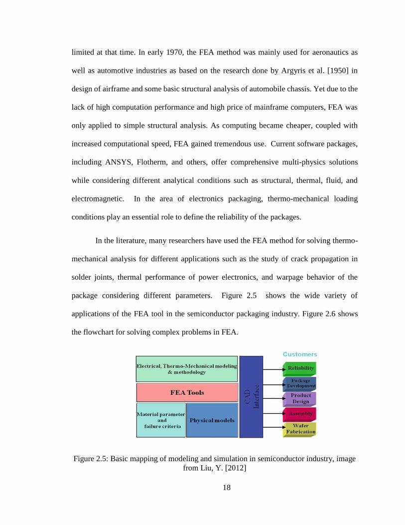
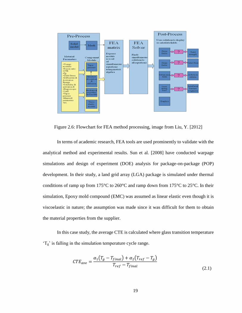
In the literature, many researchers have used the FEA method for solving thermo-
mechanical analysis for different applications such as the study of crack propagation in
solder joints, thermal performance of power electronics, and warpage behavior of the
package considering different parameters. Figure 2.5 shows the wide variety of
applications of the FEA tool in the semiconductor packaging industry. Figure 2.6 shows
the flowchart for solving complex problems in FEA.
Figure 2.5: Basic mapping of modeling and simulation in semiconductor industry, image
from Liu, Y. [2012]
19
Figure 2.6: Flowchart for FEA method processing, image from Liu, Y. [2012]
In terms of academic research, FEA tools are used prominently to validate with the
analytical method and experimental results. Sun et al. [2008] have conducted warpage
simulations and design of experiment (DOE) analysis for package-on-package (POP)
development. In their study, a land grid array (LGA) package is simulated under thermal
conditions of ramp up from 175°C to 260°C and ramp down from 175°C to 25°C. In their
simulation, Epoxy mold compound (EMC) was assumed as linear elastic even though it is
viscoelastic in nature; the assumption was made since it was difficult for them to obtain
the material properties from the supplier.
In this case study, the average CTE is calculated where glass transition temperature
‘Tg’ is falling in the simulation temperature cycle range.
𝐶𝑇𝐸𝑎𝑣𝑒 =𝛼1(𝑇𝑔 − 𝑇𝑓𝑖𝑛𝑎𝑙) + 𝛼2(𝑇𝑟𝑒𝑓 − 𝑇𝑔)
𝑇𝑟𝑒𝑓 − 𝑇𝑓𝑖𝑛𝑎𝑙
(2.1)
20
The present work demonstrates an FEA analysis based on material properties,
dimensions and other geometrical parameters from Sun et al. [2008]. This exercise helps
to estimate correct boundary and symmetry conditions of the quarter model of entire
package in order to save computational time for simulations in current studies.
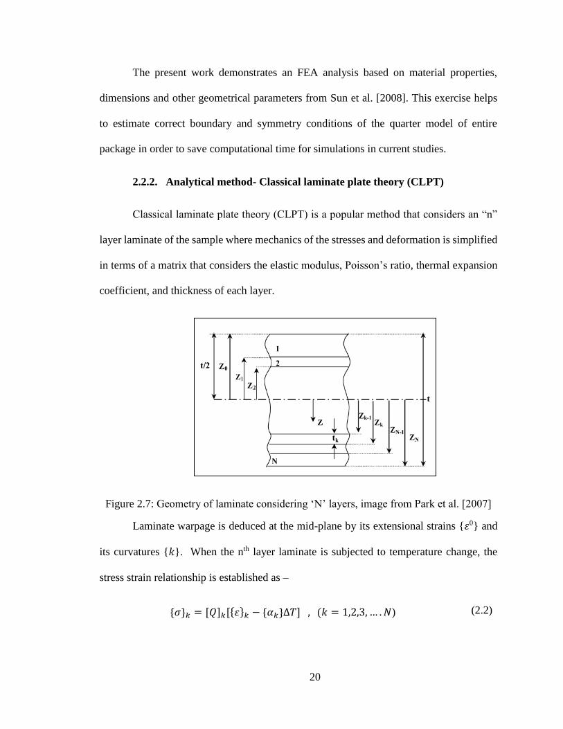
2.2.2. Analytical method- Classical laminate plate theory (CLPT)
Classical laminate plate theory (CLPT) is a popular method that considers an “n”
layer laminate of the sample where mechanics of the stresses and deformation is simplified
in terms of a matrix that considers the elastic modulus, Poisson’s ratio, thermal expansion
coefficient, and thickness of each layer.
Figure 2.7: Geometry of laminate considering ‘N’ layers, image from Park et al. [2007]
Laminate warpage is deduced at the mid-plane by its extensional strains {𝜀0} and
its curvatures {𝑘}. When the nth layer laminate is subjected to temperature change, the
stress strain relationship is established as –
{𝜎}𝑘 = [𝑄]𝑘[{𝜀}𝑘 − {𝛼𝑘}∆𝑇] , (𝑘 = 1,2,3, … .𝑁) (2.2)
21
Where, [𝑄]𝑘 =𝐸𝑘
1−𝑉𝑘2 [
1 𝑉𝑘 0𝑉𝑘 1 0
0 01−𝑉𝑘
2
]
(2.3)
For calculating[𝑄]𝑘 , the material is considered to be isotropic and Ek and Vk
represent the elastic modulus and Poisson’s ratio of the kth layer, respectively. The
relationship between plane stress {𝜀0} , curvature {𝑘}, and resultant forces {N}Λ and
moments{M}Λ is given as –
Where,
{NΛ} = ∑ ∫ [Qij]k
{Λk}zk
zk−1dzn
k=1 = ∑ [Qij]k{Λk}(zk − zk−1)
nk=1
(2.5)
{MΛ} = ∑ ∫ [Qij]k
{Λk}zk
zk−1zdzn
k=1 =1
2∑ [Qij]k
nk=1 {Λk}(zk
2 −
zk−12 )
(2.6)
{Λk} = αk∆T {110}
(2.7)
[A], [B], and [D] stiffness matrices are,
[A] = ∑∫ [Qij]dzzk
zk−1
n
k=1
= ∑[Qij]k(zk − zk−1)
n
k=1
(2.8)
[B] = ∑ ∫ [Qij]zdzzk
zk−1
n
k=1
=1
2∑[Qij]k
(zk2 − zk−1
2 )
n
k=1
(2.9)
{𝜀0
𝑘} = [
𝐴 𝐵𝐵 𝐷
]−1
{𝑁
Λ
𝑀Λ
} (2.4)
22
[D] = ∑ ∫ [Qij]z2dz
zk
zk−1
n
k=1
=1
3∑[Qij]k
(zk3 − zk−1
3 )
n
k=1
(2.10)
Middle surface curvature (𝑤0) can be calculated as follows-
[
𝑘𝑥
𝑘𝑦
𝑘𝑘𝑦
] = −
[
𝜕2𝑤0
𝜕𝑥2
𝜕2𝑤0
𝜕𝑦2
2𝜕2𝑤0
𝜕𝑥𝜕𝑦]
(2.11)
And out-of-plane deformation is calculated as,
ω = −1
2(kxx
2 + kyy2 + 2kxyxy)
(2.12)
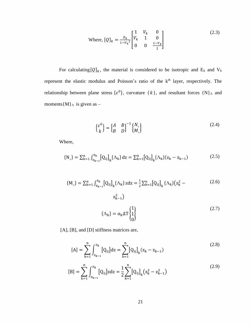
Park et al. [2007] have used this method for prediction of warpage in the chip scale
packages (CSP) and for a flip chip package with large substrate considered as package with
overhang.
Figure 2.8: Geometry of Package highlighting the overhang, image from Park et al.
[2007]
23
Out-of-plane deformation at the end of the chip in the X-direction is given by,
𝑤𝑐𝑥= −
1
2(𝑘𝑥𝑥
2)
(2.13)
For overhang portion, out-of-plane deformation in the X-direction is,
𝑤𝑜ℎ𝑥= 𝐿𝑐𝑥
𝐿𝑜ℎ𝑥𝑘𝑥
(2.14)
Total out-of-plane deformation in the X-direction is,
𝑤𝑥 = 𝑤𝑐𝑥+ 𝑤𝑜ℎ𝑥
(2.15)
Similarly, in the Y-direction,
𝑤𝑦 = 𝑤𝑐𝑦+ 𝑤𝑜ℎ𝑦
(2.16)
By using the formulae given above and FEA method, Park et al. [2007] have
developed a predictive model for optimized design parameters in flip chip package and
assemblies. In that work, they have studied the importance of applying appropriate
effective moduli of the material when there is composite structure of solder joints covered
in underfill.
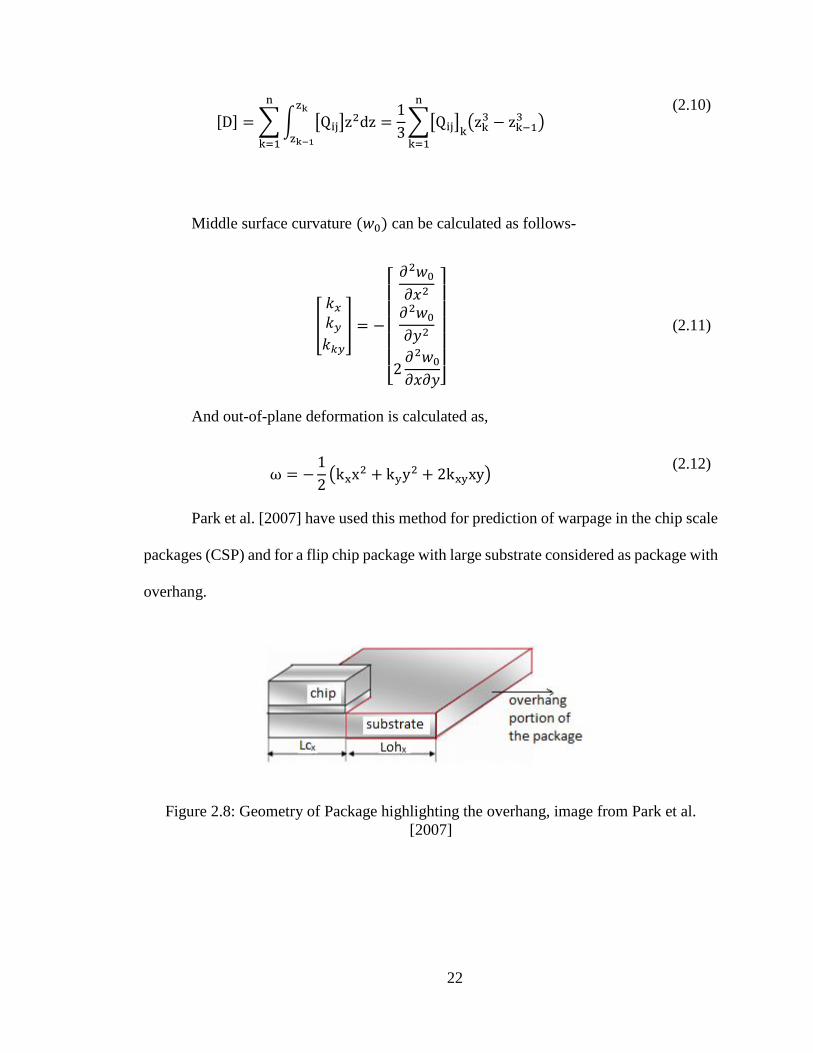
24
Figure 2.9: Geometry of Package highlighting the layer where effective material
properties are to be considered
The effective material property of the composite layer is calculated using a
simplified formula as follows,
Eeffective =ESolderVSolder + EUnderfillVUnderfill
VSolder + VUnderfill
(2.17)
µeffective
=µ
SolderVSolder + µ
UnderfillVUnderfill
VSolder + VUnderfill
(2.18)
αeffective =αSolderESolderVSolder + αUnderfillEUnderfillVUnderfill
ESolderVSolder + EUnderfillVUnderfill
(2.19)
Where, Eeffective , µeffective
, αeffective are elastic modulus, Poisson’s ratio, and
coefficient of thermal expansion (CTE) of the composite layer, respectively. And
conclusion the study as for composite layer considered to be isotropic then in-plane
effective moduli are more appropriate than out-of-plane.
2.2.3. Modified Suhir’s solution
Later, a study presented by Tsai et al. [2009] suggested that classical lamination
theory assumes that radius of curvature is constant with respect to the Kirchhoff- Love
hypothesis. So, the formula mentioned above becomes invalid and provides more errors as
25
the die attach layer is more compliant. Tsai et al. [2009] suggested the modified Suhir’s
[1980] solution for simplified flip chip package represented in Figure 2.10.
Figure 2.10: Schematic of simplified flip chip package
There are certain assumptions included in this theory; one such assumption, for
example, is that isothermal loading is applied on the package and that there is a perfectly
bonded interface between each layer. Also, each layer acts as a spherically bending thin
plate. Due to there being a small thickness, along with the underfill layer and material being
compliant with the die and substrate, the CTE of the underfill is insensitive to stresses and
therefore neglected.
Warpage is ,
𝑤(𝑥) =𝑡∆𝛼∆𝑇
2𝜆𝐷[1
2𝑥2 −
cosh 𝑘𝑥 − 1
𝑘2 cosh 𝑘𝑙 ]
(2.20)
And radius of curvature is,
Where, ∆𝑇 is difference between final temperature and initial temperature and ∆𝛼
is CTE mismatch between the adjacent layers of the package.
1
𝜌(𝑥)=
𝑡∆𝛼∆𝑇
2𝜆𝐷(1 −
𝑐𝑜𝑠ℎ𝑘𝑥
cosh 𝑘𝑙 )
(2.21)
26
𝑘 = √𝜆
𝜅
(2.22)
𝜆 = 1 − 𝜈𝑑𝑖𝑒
𝐸𝑑𝑖𝑒𝑡𝑑𝑖𝑒+
1 − 𝜈𝑠𝑢𝑏𝑠𝑡𝑟𝑎𝑡𝑒
𝐸𝑠𝑢𝑏𝑠𝑡𝑟𝑎𝑡𝑒𝑡𝑠𝑢𝑏𝑠𝑡𝑟𝑎𝑡𝑒+
𝑡2
4𝐷
(2.23)
Here, t is the total thickness and is flexural rigidity of the package, calculated as,
𝑡 = 𝑡𝑑𝑖𝑒 + 𝑡𝑑𝑖𝑒 𝑎𝑡𝑡𝑎𝑐ℎ + 𝑡𝑠𝑢𝑏𝑠𝑡𝑟𝑎𝑡𝑒 (2.24)
𝐷 = 𝐷𝑑𝑖𝑒 + 𝐷𝑑𝑖𝑒 𝑎𝑡𝑡𝑎𝑐ℎ + 𝐷𝑠𝑢𝑏𝑠𝑡𝑟𝑎𝑡𝑒 (2.25)
𝐷 = ∑𝐸𝑖𝑡𝑖
3
12(1 − 𝜈𝑖)
(2.26)
𝜅 =𝑡𝑑𝑖𝑒
3𝐺𝑑𝑖𝑒+
2𝑡𝑑𝑖𝑒𝑎𝑡𝑡𝑎𝑐ℎ
3𝐺𝑑𝑖𝑒𝑎𝑡𝑡𝑎𝑐ℎ+
𝑡𝑆𝑢𝑏𝑠𝑡𝑟𝑎𝑡𝑒
3𝐺𝑆𝑢𝑏𝑠𝑡𝑟𝑎𝑡𝑒
(2.27)
Here, E, 𝜈 and G are, respectively, elastic modulus, Poisson’s ratio, and shear
modulus of the material. Based on their study it is concluded by Tsai et al. [2009] that low
elastic moduli of the underfill can significantly reduce the maximum warpage and it was
suggested to use either a low modulus of the underfill or low CTE for the substrate to
reduce maximum warpage effect.
2.3. Summary
The literature available on the warpage measurements of the electronic packages
mainly focuses on the warpage on the entire package, typically at the mid plane of the
package. Taking into consideration the total thickness of the package, this mid plane lies
closer to the PCB/substrate rather than the lid. There are limited studies that analyze or
report measurements of warpage in the lid of an electronics package. In this research work,
27
performance of the package under thermo-mechanical loading in terms of warpage on the
lid of the package is analyzed using a combination of FEA and DOE analyses. The effect
of different parameters in the design process of the lid of the package are investigated using
FEA simulations. These parameters include the material properties, shape and different
thickness of the lid on the package. Dasgupta et al. [1998] have discussed an approach for
design of experiment methods for parametric study in electronics packaging. In a
subsequent chapter, a similar approach using design of experiment methods is applied to
investigate the effect of different parameters on the lid.
28
3. Research Methodology
The previous chapter discussed different methods of estimating warpage of
electronics packages. Considering the availability of resources for this project, a
combination of FEA analysis and analytical methods is employed. In formulating the FEA
simulation a case study derived by Sun et al. [2008] has proven helpful to understand the
correct boundary conditions and thermo-mechanical loading setup. In that study, the
warpage of the package is measured across the diagonal to estimate accurately the
magnitude as well as nature of the warpage. The details of the case study and further
research work as follows.
3.1. Research Experiment – Case study
In order to collect data for design of experiments analysis, simulations were
performed by using FEA software ANSYS 17.0. The research methodology is developed
based on the case study solved as given by W. Sun et al. [2008]. An LGA package is
simulated under thermal loading conditions of cooling from 175°C to 25°C and heating
from 175°C to 260°C with stress-free state assumed at 175°C. Material properties and
dimensions were considered as shown in Table 3.1.
29
Table 3.1: Dimensional details and Material properties of different layers in LGA package,
Sun et al. [2008]
LGA
layers
Length×
Width Thickness
Young's
modulus
at 25°C
Young's
modulus
at 260°C
CTE at 25°C CTE at
260°C Tg
Unit (mm) (MPa) (ppm/°C) (°C)
Die 5×9.7 0.1 131000 2.6 -
Die
attach 5×9.7 0.04 230 5 41 172 41
EMC
8×10.5
0.35 24000 280 9 36 135
SM 0.03 2400 800 60 130 100
Core 0.1 28000 8600 *XY:14,Z:30 XY:7, Z:150 220
Cu 0.02 11700 17.3 -
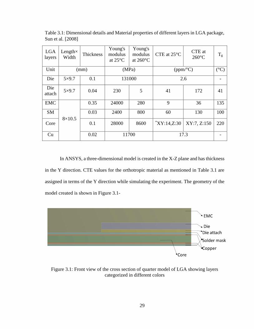
In ANSYS, a three-dimensional model is created in the X-Z plane and has thickness
in the Y direction. CTE values for the orthotropic material as mentioned in Table 3.1 are
assigned in terms of the Y direction while simulating the experiment. The geometry of the
model created is shown in Figure 3.1-
Figure 3.1: Front view of the cross section of quarter model of LGA showing layers
categorized in different colors
30
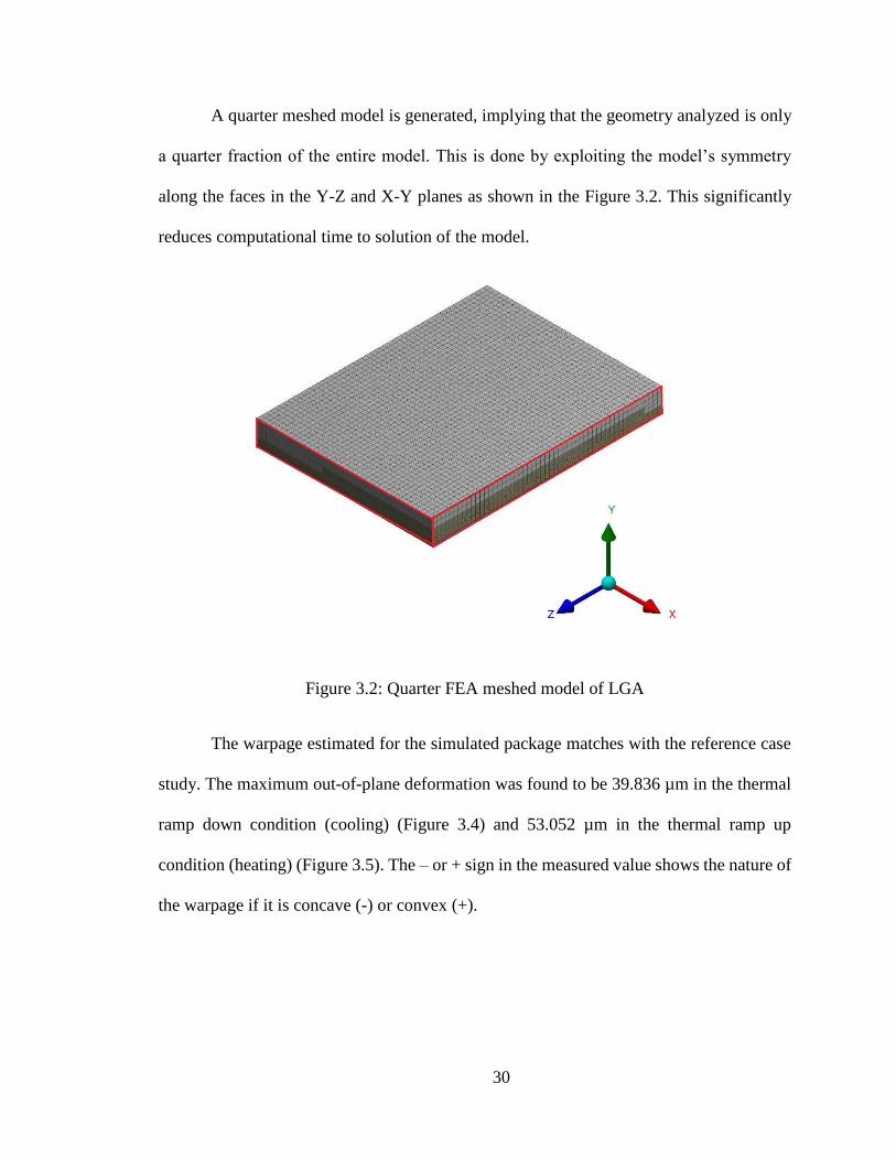
A quarter meshed model is generated, implying that the geometry analyzed is only
a quarter fraction of the entire model. This is done by exploiting the model’s symmetry
along the faces in the Y-Z and X-Y planes as shown in the Figure 3.2. This significantly
reduces computational time to solution of the model.
Figure 3.2: Quarter FEA meshed model of LGA
The warpage estimated for the simulated package matches with the reference case
study. The maximum out-of-plane deformation was found to be 39.836 µm in the thermal
ramp down condition (cooling) (Figure 3.4) and 53.052 µm in the thermal ramp up
condition (heating) (Figure 3.5). The – or + sign in the measured value shows the nature of
the warpage if it is concave (-) or convex (+).
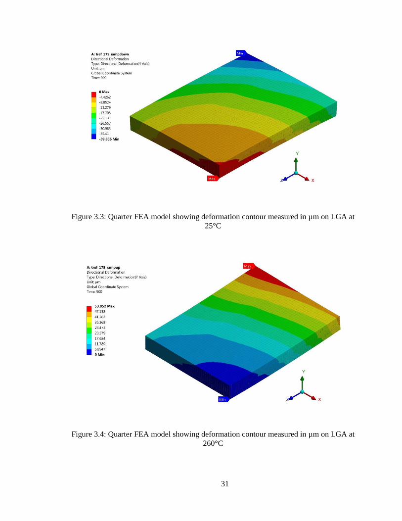
31
Figure 3.3: Quarter FEA model showing deformation contour measured in µm on LGA at
25°C
Figure 3.4: Quarter FEA model showing deformation contour measured in µm on LGA at
260°C
32
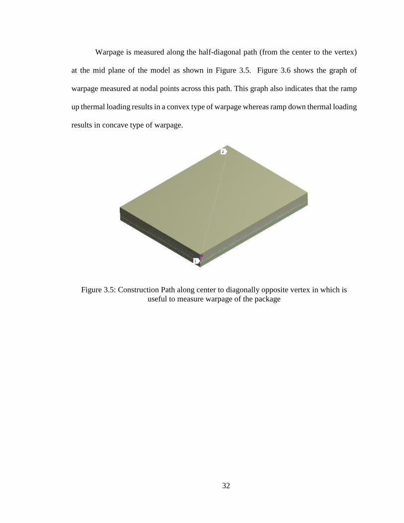
Warpage is measured along the half-diagonal path (from the center to the vertex)
at the mid plane of the model as shown in Figure 3.5. Figure 3.6 shows the graph of
warpage measured at nodal points across this path. This graph also indicates that the ramp
up thermal loading results in a convex type of warpage whereas ramp down thermal loading
results in concave type of warpage.
Figure 3.5: Construction Path along center to diagonally opposite vertex in which is
useful to measure warpage of the package
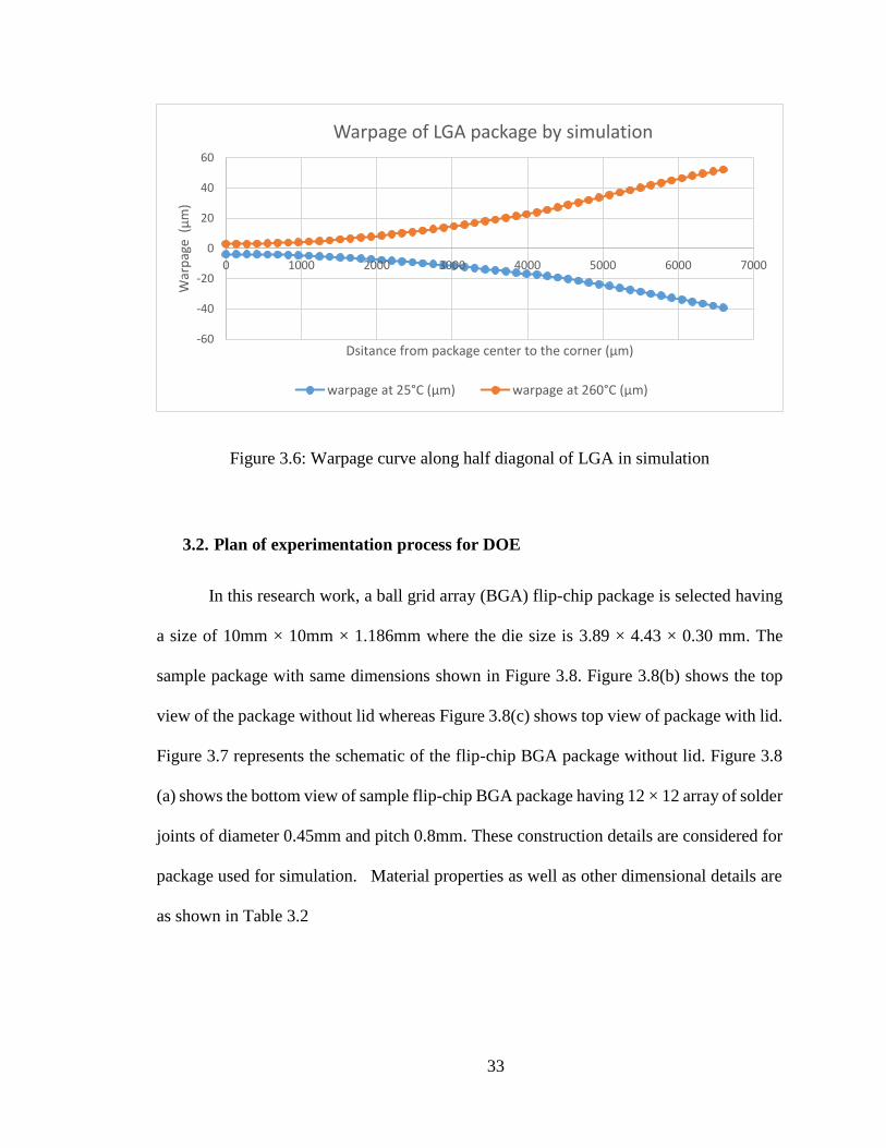
33
Figure 3.6: Warpage curve along half diagonal of LGA in simulation
3.2. Plan of experimentation process for DOE
In this research work, a ball grid array (BGA) flip-chip package is selected having
a size of 10mm × 10mm × 1.186mm where the die size is 3.89 × 4.43 × 0.30 mm. The
sample package with same dimensions shown in Figure 3.8. Figure 3.8(b) shows the top
view of the package without lid whereas Figure 3.8(c) shows top view of package with lid.
Figure 3.7 represents the schematic of the flip-chip BGA package without lid. Figure 3.8
(a) shows the bottom view of sample flip-chip BGA package having 12 × 12 array of solder
joints of diameter 0.45mm and pitch 0.8mm. These construction details are considered for
package used for simulation. Material properties as well as other dimensional details are
as shown in Table 3.2
-60
-40
-20
0
20
40
60
0 1000 2000 3000 4000 5000 6000 7000
War
pag
e (
µm
)
Dsitance from package center to the corner (µm)
Warpage of LGA package by simulation
warpage at 25°C (µm) warpage at 260°C (µm)
34
Figure 3.7: Schematic of package of without lid
Figure 3.8: (a) Bottom view of the flip chip BGA package (b) Top view of the
package without lid (c) Top view of the package with lid
Table 3.2: Dimensional details and Material properties of different layers in package used
for experiment
Material
layers
Length ×
Width Thickness
Young's
modulus
Poisson's
ratio CTE Tg
Unit (mm) (GPa) - (ppm/°C) (°C)
Die 3.89 × 4.43 0.3 131 0.3 2.6
-
PCB 15 × 15 0.5 242 0.11 19.60
Solder
joints Φ 0.45 pitch 0.8 416 0.35 21.70
Substrate 10 × 10 0.34 23 0.3 15
Thermal
interface
material
3.89 × 4.43 0.12 0.163 0.3 1.92
Underfill +
bump 5.5 × 5.5 0.08
17.41 @
-55 °C,
14.68 @
225°C
0.35
26.58
(T<Tg),
60.84
(T>Tg)
88
(
c)
35
An underfill with micro bumps and a substrate with pre-preg layers are treated as
composite materials and their material properties are included in Table 3.2. These are
effective material properties calculated by using Equations 2.17, 2.18, and 2.19 as
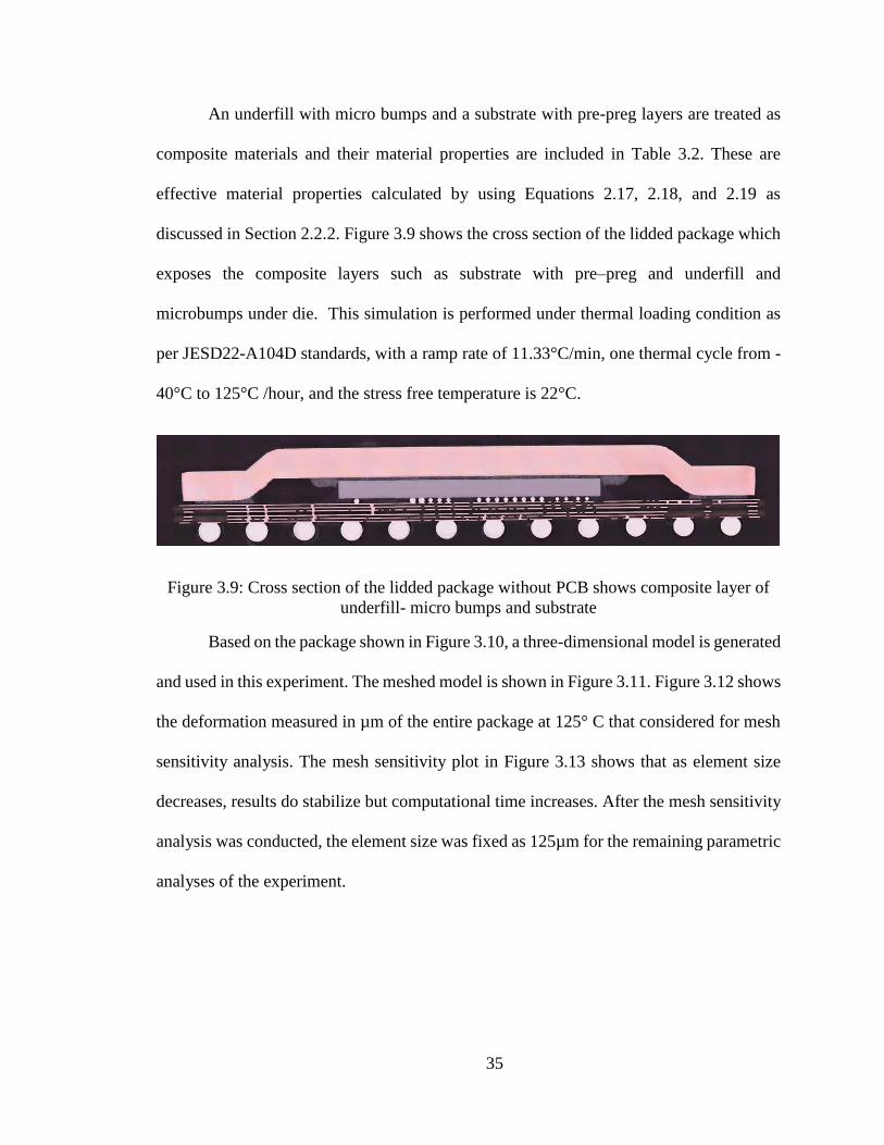
discussed in Section 2.2.2. Figure 3.9 shows the cross section of the lidded package which
exposes the composite layers such as substrate with pre–preg and underfill and
microbumps under die. This simulation is performed under thermal loading condition as
per JESD22-A104D standards, with a ramp rate of 11.33°C/min, one thermal cycle from -
40°C to 125°C /hour, and the stress free temperature is 22°C.
Figure 3.9: Cross section of the lidded package without PCB shows composite layer of
underfill- micro bumps and substrate
Based on the package shown in Figure 3.10, a three-dimensional model is generated
and used in this experiment. The meshed model is shown in Figure 3.11. Figure 3.12 shows
the deformation measured in µm of the entire package at 125° C that considered for mesh
sensitivity analysis. The mesh sensitivity plot in Figure 3.13 shows that as element size
decreases, results do stabilize but computational time increases. After the mesh sensitivity
analysis was conducted, the element size was fixed as 125µm for the remaining parametric
analyses of the experiment.
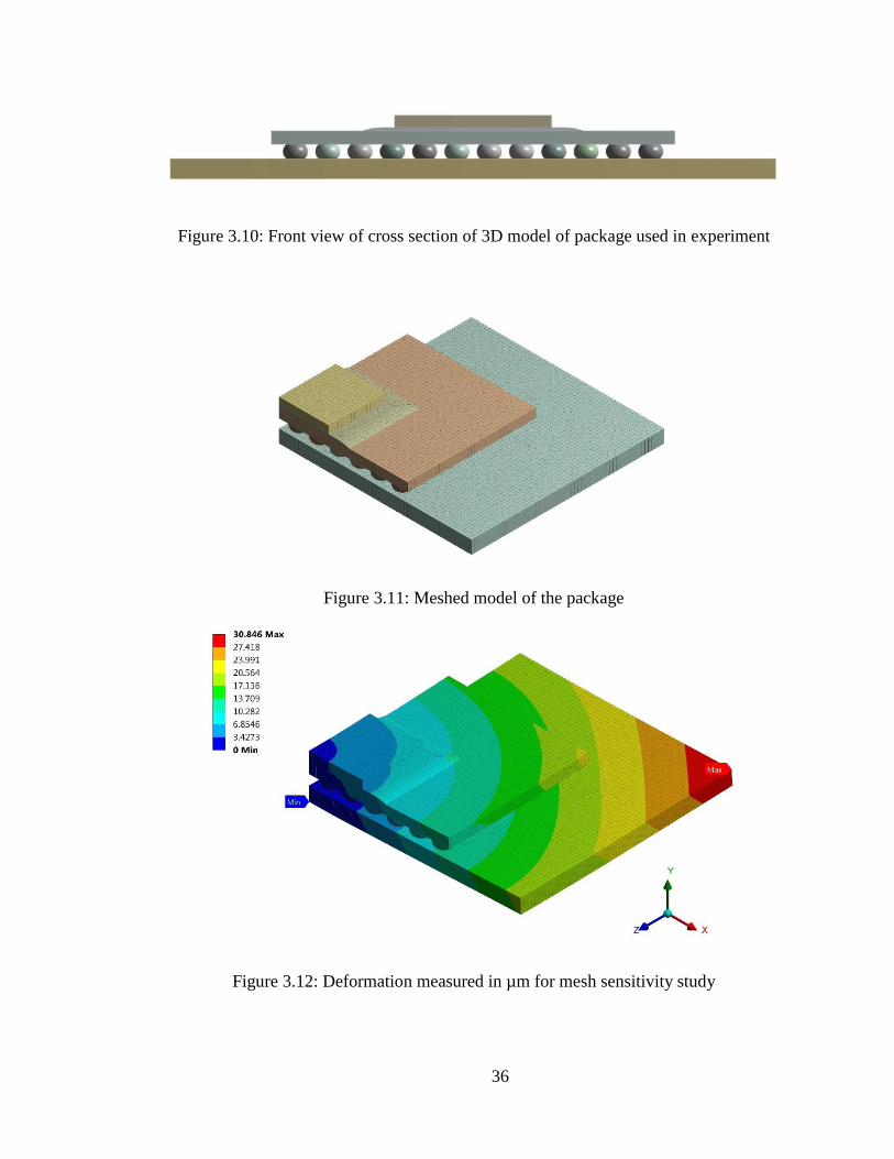
36
Figure 3.10: Front view of cross section of 3D model of package used in experiment
Figure 3.11: Meshed model of the package
Figure 3.12: Deformation measured in µm for mesh sensitivity study
37
Figure 3.13: Mesh sensitivity on the baseline model
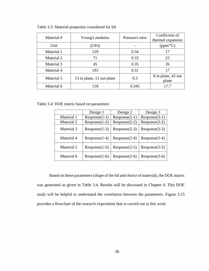
After the meshing parameters and design parameters for the baseline case are
finalized, different shape and materials are considered for the design of the lid over package.
Different shapes are considered as shown in Figure 3.14.
Figure 3.14: Different shapes considered for lid
Materials considered for the lid are as shown in Table 3.3.
30.5
31
31.5
32
32.5
33
0 100 200 300 400 500 600 700 800 900 1000 1100
Dir
ecti
on
def
orm
atio
n (
µm
)
Element size (µm)
Mesh sensitivity on the baseline model
38
Table 3.3: Material properties considered for lid
Material # Young's modulus Poisson's ratio Coefficient of
thermal expansion
Unit (GPa) - (ppm/°C)
Material 1 129 0.34 17
Material 2 71 0.33 23
Material 3 45 0.35 26
Material 4 193 0.31 17
Material 5 13 in plane, 11 out plane 0.3 8 in plane, 42 out
plane
Material 6 118 0.345 17.7
Table 3.4: DOE matrix based on parameters
Design 1 Design 2 Design 3
Material 1 Response(1-1) Response(2-1) Response(3-1)
Material 2 Response(1-2) Response(2-2) Response(3-2)
Material 3 Response(1-3) Response(2-3) Response(3-3)
Material 4 Response(1-4) Response(2-4) Response(3-4)
Material 5 Response(1-5) Response(2-5) Response(3-5)
Material 6 Response(1-6) Response(2-6) Response(3-6)
Based on these parameters (shape of the lid and choice of material), the DOE matrix
was generated as given in Table 3.4. Results will be discussed in Chapter 4. This DOE
study will be helpful to understand the correlation between the parameters. Figure 3.15
provides a flowchart of the research experiment that is carried out in this work.
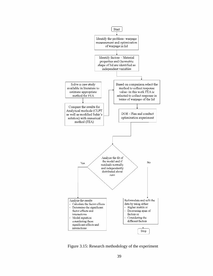
39
Figure 3.15: Research methodology of the experiment
40
3.3. Summary
In conclusion, an FEA formulation was developed for generation of warpage data
for a subsequent design of experiments analysis presented in Chapter 4. FEA simulations
were carried out on 3 different lid designs and 6 different materials leading to a data set of
18 warpage predictions. The material properties that are known to vary across the 6
materials include Young’s modulus, Poisson’s ratio and coefficient of thermal expansion.
Among the, the young’s modulus varied the most from 11 GPa in the lowest case to 193
GPa in the highest. The CTE data varied within an order of magnitude between the best
and worst cases. Assuming that the loading on the package lid leads to an induced warpage
that is within the elastic region, these predictions are reliable. A mesh sensitivity study
showed that computational time could be optimized and a mesh size / parameter of ‘125µm’
was selected such that any further reduction in mesh size would lead to no change in the
warpage prediction.
41
4. Results and Discussion
As discussed in the previous chapters based on the LGA case study, experiment of
simulation carried out. This experiment involved 6 type of material parameters and 3 types
of design parameters. Total 18 simulation runs performed excluding baseline case of
package without lid. This baseline is used only for mesh sensitivity analysis to avoid effect
of parameters related to lid which are variables on response value of warpage. In this
chapter, Comparison of the warpage evaluated by using FEA and analytical methods and
design of experiment study is discussed as follows.
4.1. Comparison of results for analytical methods and FEA method
The analytical model of the CLPT three layer of package consists of the die,
underfill and microbumps, and the substrate layer. FEA simulation is performed using
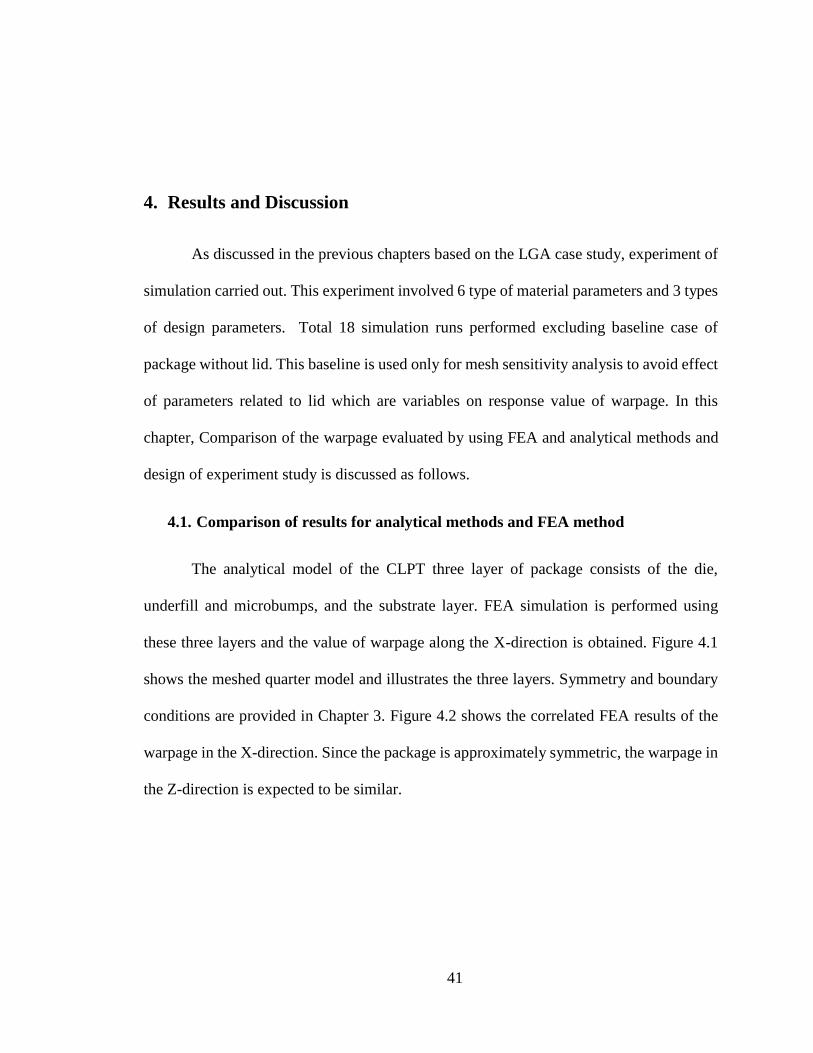
these three layers and the value of warpage along the X-direction is obtained. Figure 4.1
shows the meshed quarter model and illustrates the three layers. Symmetry and boundary
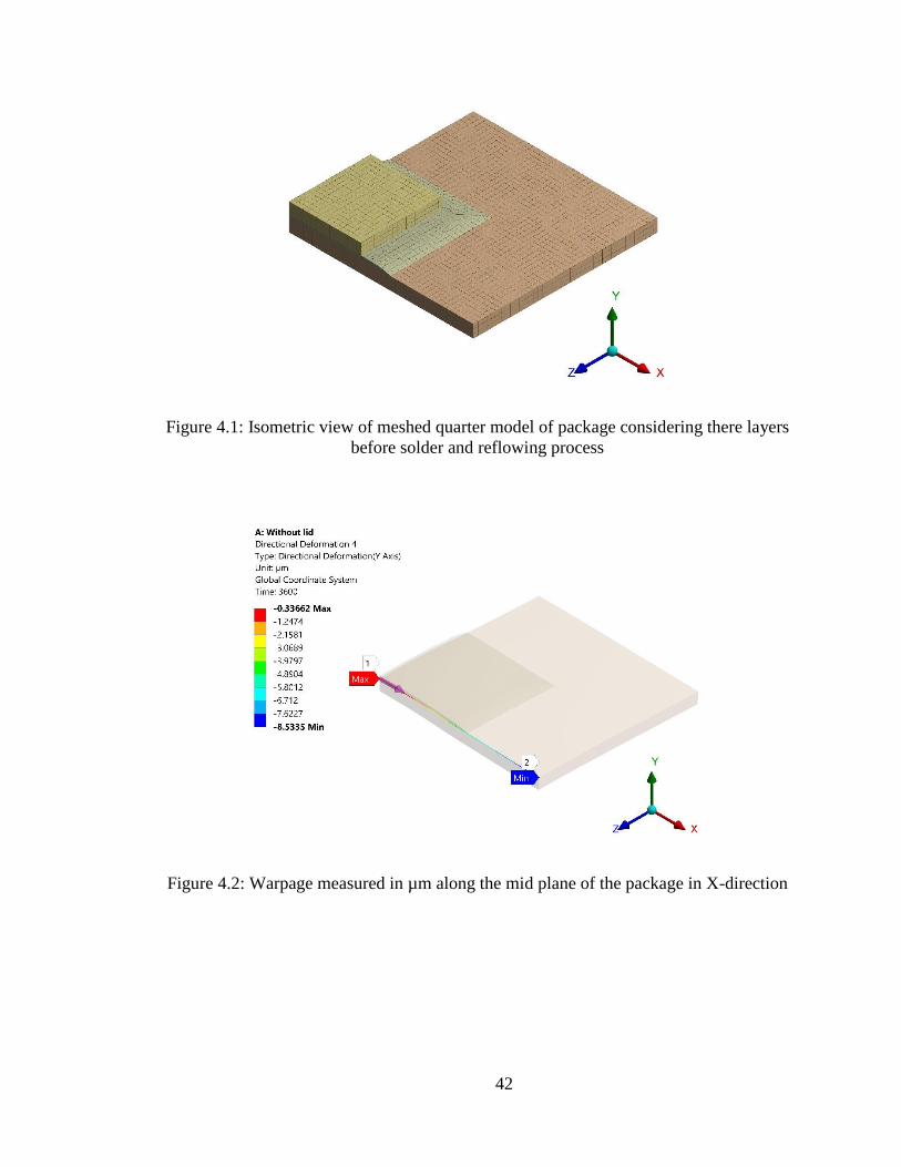
conditions are provided in Chapter 3. Figure 4.2 shows the correlated FEA results of the
warpage in the X-direction. Since the package is approximately symmetric, the warpage in
the Z-direction is expected to be similar.
42
Figure 4.1: Isometric view of meshed quarter model of package considering there layers
before solder and reflowing process
Figure 4.2: Warpage measured in µm along the mid plane of the package in X-direction
43
As per the analytical methods discussed in Section 2.2.2, values of the material
properties and thickness of the material are utilized in the equations. Warpage is calculated
in the X-direction using Equations 2.2 - 2.27.
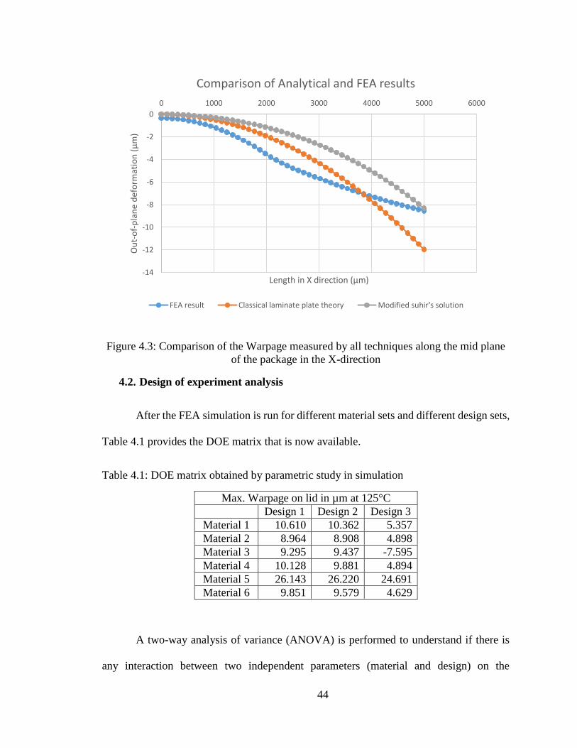
Figure 4.3 shows that analytical results provide a fall-off shaped curve in which the
effect of CTE of underfill material is considered insensitive to stresses and neglected due
overall to small thickness of the underfill layer. Whereas the FEA result provides an s-
shaped curve which seems more accurate as it considers the effect of the underfill.
In this curve, it is also evident that in classical laminate plate theory that assumes
radius of curvature is constant with respect to Krichoff-love hypothesis. . This hypothesis
is used to determine stress and deformation of thin layers when those are subjected to force
and moment. The assumptions of this hypothesis that are the thickness of the layer is
constant during deformation and straight lines normal to mid surface remains normal and
straight after the deformation. This leads to more error in calculating response in terms of
warpage. Due to this error, the classical laminate plate theory over-predicts the out-of-plane
deformation by 40%. This highlights the substantially higher accuracy of FEA method that
is presented in this work.
44
Figure 4.3: Comparison of the Warpage measured by all techniques along the mid plane
of the package in the X-direction
4.2. Design of experiment analysis
After the FEA simulation is run for different material sets and different design sets,
Table 4.1 provides the DOE matrix that is now available.
Table 4.1: DOE matrix obtained by parametric study in simulation
Max. Warpage on lid in µm at 125°C Design 1 Design 2 Design 3
Material 1 10.610 10.362 5.357
Material 2 8.964 8.908 4.898
Material 3 9.295 9.437 -7.595
Material 4 10.128 9.881 4.894
Material 5 26.143 26.220 24.691
Material 6 9.851 9.579 4.629
A two-way analysis of variance (ANOVA) is performed to understand if there is
any interaction between two independent parameters (material and design) on the
-14
-12
-10
-8
-6
-4
-2
0
0 1000 2000 3000 4000 5000 6000
Ou
t-o
f-p
lan
e d
efo
rmat
ion
(µ
m)
Length in X direction (µm)
Comparison of Analytical and FEA results
FEA result Classical laminate plate theory Modified suhir's solution
45
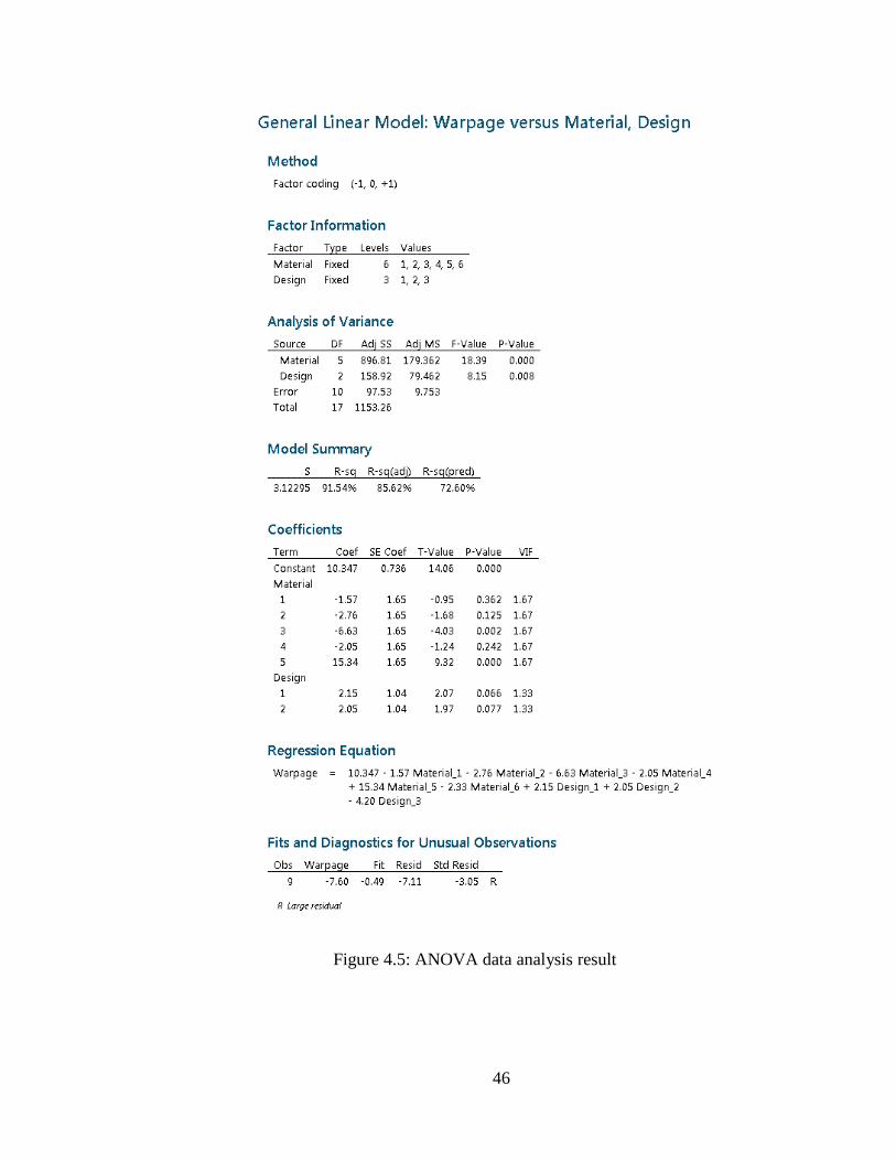
dependent variable (warpage). For this analysis, the null hypothesis for a main effect is that
the warpage means for all factor levels are equal and an interaction effect is that the
warpage mean for the level of material factor does not depend on the value of the other
levels of design factor.
In this analysis, the p value is less than the significance level as shown in Figure
4.5, indicating that the level of material and design factor is associated with warpage of the
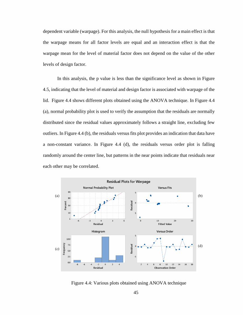
lid. Figure 4.4 shows different plots obtained using the ANOVA technique. In Figure 4.4
(a), normal probability plot is used to verify the assumption that the residuals are normally
distributed since the residual values approximately follows a straight line, excluding few
outliers. In Figure 4.4 (b), the residuals versus fits plot provides an indication that data have
a non-constant variance. In Figure 4.4 (d), the residuals versus order plot is falling
randomly around the center line, but patterns in the near points indicate that residuals near
each other may be correlated.
Figure 4.4: Various plots obtained using ANOVA technique
46
Figure 4.5: ANOVA data analysis result
47
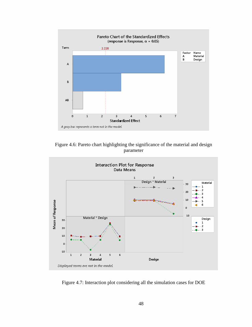
In addition to two-way ANOVA, the DOE is performed using a general full
factorial analysis. This analysis considers the interaction between the material and design
parameters and results in missing values of p and F. This is due to the use of a 2-level
design with one replicate, including all the terms in the model. To remedy this situation,
the model is re-fit neglecting the interaction term between the material and design factors.
The Pareto chart in Figure 4.6 shows that the interaction between material and design
parameter is not significant. If the material parameter is compared with design then it
indicates that the material parameter is more significant than the design parameter. The
interaction plot between material and design parameter in Figure 4.7 shows near
parallelism. This supports the assumption of an absence of interaction between two
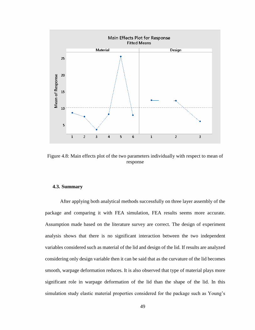
parameters. The main effects plot with warpage in Figure 4.8 shows that Material 5 has the
highest response value where Design 3 has the lowest. This might be interpreted as the
Design 3 shape causes the minimum warpage and Material 5 is more elastic in nature and
gives maximum warpage. It is difficult to predict the plastic/permanent damage
considering only elastic behavior of the material. It can be interpreted from the main effects
plot that since the curvature of the lid is smoother, then the deformation is minimum.
48
Figure 4.6: Pareto chart highlighting the significance of the material and design
parameter
Figure 4.7: Interaction plot considering all the simulation cases for DOE
49
Figure 4.8: Main effects plot of the two parameters individually with respect to mean of
response
4.3. Summary
After applying both analytical methods successfully on three layer assembly of the
package and comparing it with FEA simulation, FEA results seems more accurate.
Assumption made based on the literature survey are correct. The design of experiment
analysis shows that there is no significant interaction between the two independent
variables considered such as material of the lid and design of the lid. If results are analyzed
considering only design variable then it can be said that as the curvature of the lid becomes
smooth, warpage deformation reduces. It is also observed that type of material plays more
significant role in warpage deformation of the lid than the shape of the lid. In this
simulation study elastic material properties considered for the package such as Young’s
50
modulus, Poisson’s ratio and Coefficient of thermal expansion. Out of these three material
properties coefficient of thermal expansion should be more compliant to other layer in the
package in order to reduce warpage. Experimental procedures to measure warpage may
prove more accurate than analytical and numerical methods. Since ultimate strength and
plastic behavior of the material will be tested while thermal loading conditions applied.
Although, thermal loading will be accelerated, due to fatigue and creep phenomenon
involved warpage result will account for reliability in real life conditions. This is difficult
to achieve by FEA tools or analytical tools. So experimental procedure of measuring this
parametric study is important in future work to gain more accurate predictions.
51
5. Conclusions and Future Work
In this thesis, a DOE analysis is conducted on simulated data from warpage of a
lidded electronics package using an FEA approach. Warpage in a lid of an optical
electronics package can detrimentally affect the reliability of the package as well as its
optical performance. The present study focuses on the variety of materials and designs of
lids relevant to recent technologies in electronics packaging.
The thesis begins with a review of various methods for warpage measurements
demonstrated in the literature, including experimental, numerical, and analytical methods.
In a detailed review, various experimental methods are compared based on the properties
such as resolution, cost, accuracy, capacity for in-line measurement, flexibility, etc. It is
evident that Shadow moiré is the most suitable procedure while digital fringe projection is
the second best choice. Other methods, such as digital image correlation, projection moiré,
Twyman–Green interferometry, and Fizeau interferometry, have similar performance; but,
based on the application, these methods are selected by users. Next, a brief overview of the
classical laminate plate theory is presented followed by a literature review of previous work
using numerical techniques applied to thermo-mechanical analysis of electronics packages.
52
In Chapter 3, a FEA is formulated to generate data for this study, owing its
tremendous versatility and accuracy in predicting deformations of simple geometries such
as those considered herein. The boundary conditions applied to the package geometry
exploit its symmetry. The measured value for the warpage on LGA matches with case study
recreated as per reference. Additionally, a mesh sensitivity study is also conducted which
leads to a significant reduction in computational time and resources.
In Chapter 4, data and results from the FEA are presented and compared to
analytical calculations using the CLPT. Finally, these data are used to conduct a DOE
analysis to investigate the influence of 3 distinct designs and 6 material choices on warpage
of a lid. The key findings from this work can be summarized as follows:
1. Comparisons of warpage estimated from FEA and analytical methods (either by CLPT
or modified Suhir’s theory) show that FEA results are more accurate as they account
for the performance of die attach/underfill materials, regardless of the small thickness
of the layer.
2. Between CLPT and modified Suhir’s theory, the latter is more accurate since it does
not consider the radius of curvature of deformation to be constant.
3. The DOE analysis indicates that there is no significant interaction between the two
parameters (lid design and material) considered to affect the warpage in the lid. Hence,
they can be considered independent variables in the experiments.
4. Material properties of the lid have a more substantial effect on the warpage of the lid
as compared to variability in lid design.
5. It is worth mentioning that these FEA simulations are performed considering material
behavior within the elastic limit. In some situations, plastic deformation may occur
53
which is more permanent and can be measured more accurately via experimental
techniques.
Now, a description of some areas of suggested future work is described.
Experimental methods can be employed to measure warpage in electronic package lids to
generate more robust data for DOE analyses. Such data could better account for plastic
behavior of materials as compared to FEA. This is difficult in FEA because plasticity data
are not easily available from manufacturers for these materials. Secondly, since the
package was approximately symmetric, the behavior in the X-direction was assumed as
same for the behavior of other in-plane directions i.e. Z-direction. Verifying this
assumption may be of importance. Another approach could be to measure data such as
ultimate strength or visco-plastic parameters of these materials and feed them back into
FEA analysis in the plastic region.
54
6. References Cited
1. Standard, J. E. D. E. C. (2009). Package warpage measurement of surface-mount
integrated circuits at elevated temperature. JESD22-B112 October 2009. Available on
http://www.insidix.com/uploads/tx_bihopendoc/Jedec_22B112A_1_.pdf (accessed May
20, 2017).
2. Kang, Sungbum, and I. Charles Ume. "Techniques for Measuring Warpage of Chip
Packages, PWBs, and PWB Assemblies." IEEE Transactions on Components, Packaging
and Manufacturing Technology 3, no. 9 (2013): 1533-1544
3. Park, Seungbae, H. C. Lee, Bahgat Sammakia, and Karthik Raghunathan.
"Predictive model for optimized design parameters in flip-chip packages and
assemblies." IEEE Transactions on Components and Packaging Technologies 30, no. 2
(2007): 294-301.
4. Fischer, Jerry. Handbook of molded part shrinkage and warpage. William Andrew,
2012.
5. Hartsough, C., A. Goswami, C. Jang, and B. Han. "Advanced co-planarity
measurement tools for the warpage investigation of non-conventional packages caused by
reflow and assembly process." In Electronic Components and Technology Conference,
2007. ECTC'07. Proceedings. 57th, pp. 767-772. IEEE, 2007.
6. Pan, Jiahui, Ryan Curry, Neil Hubble, and Dirk Zwemer. "Comparing techniques
for temperature-dependent warpage measurement." Plus 10 (2007): 1980-1985.
7. Schwarz, Bernd. "Deformation measurements used for design optimization and
verification during industrial electronic board (product) manufacturing." In Electronic
Packaging Technology, 2007. ICEPT 2007. 8th International Conference on, pp. 1-5.
IEEE, 2007.
8. Arruda, Luciano, Luanda Marinho, Edson Silva, and Willy Machado. "Flexible
Circuits with embedded resistors subjected to extreme thermal loading conditions using
the Shadow Moiré and FEM measurements techniques." In Thermal, Mechanical &
Multi-Physics Simulation, and Experiments in Microelectronics and Microsystems
(EuroSimE), 2010 11th International Conference on, pp. 1-6. IEEE, 2010.
9. Xue, Ke, Jingshen Wu, Haibin Chen, Jingbo Gai, and Angus Lam. "Warpage
prediction of fine pitch BGA by finite element analysis and shadow moiré technique."
In Electronic Packaging Technology & High Density Packaging, 2009. ICEPT-HDP'09.
International Conference On, pp. 317-321. IEEE, 2009.
55
10. Jang, Kyung-Woon, Jin-Hyoung Park, Soon-Bok Lee, and Kyung-Wook Paik. "A
study on thermal cycling (T/C) reliability of anisotropic conductive film (ACF) flip chip
assembly for thin chip-on-board (COB) packages." Microelectronics Reliability52, no. 6
(2012): 1174-1181.
11. Jang, Jae-Won, Kyoung-Lim Suk, Jin-Hyoung Park, Kyung-Wook Paik, and
Soon-Bok Lee. "Warpage Behavior and Life Prediction of a Chip-on-Flex Package Under
a Thermal Cycling Condition." IEEE Transactions on Components, Packaging and
Manufacturing Technology 4, no. 7 (2014): 1144-1151.
12. Xiong, Bingshou, Myung-June Lee, and Thomas Kao. "Warpage improvement for
large die flip chip package." In Electronics Packaging Technology Conference, 2009.
EPTC'09. 11th, pp. 40-43. IEEE, 2009.
13. Yang, D. G., K. M. B. Jansen, L. J. Ernst, G. Q. Zhang, J. G. J. Beijer, and J. H. J.
Janssen. "Experimental and numerical investigation on warpage of QFN packages induced
during the array molding process." In Electronic Packaging Technology, 2005 6th
International Conference on, pp. 94-98. IEEE, 2005.
14. Miyake, Kiyoshi. "Viscoelastic warpage analysis of surface mount
package." ASME Journal Electronic Packaging 123 (2001): 101-104.
15. Pan, Jiahui, Ryan Curry, Neil Hubble, and Dirk Zwemer. "Comparing techniques
for temperature-dependent warpage measurement." Plus 10 (2007): 1980-1985.
16. Ding, Hai, Reinhard E. Powell, Carl R. Hanna, and I. Charles Ume. "Warpage
measurement comparison using shadow moiré and projection moiré methods." IEEE
Transactions on Components and Packaging Technologies 25, no. 4 (2002): 714-721.
17. Yeh, C. P., K. Banerjee, T. Martin, C. Umeagukwu, R. Fulton, J. Stafford, and K.
Wyatt. "Experimental and analytical investigation of thermally induced warpage for
printed wiring boards." In Electronic Components and Technology Conference, 1991.
Proceedings., 41st, pp. 382-387. IEEE, 1991.
18. Bakke, Edward Wight, and Chris Argyris. Organizational Structure and Dynamics:
A Framework for Theory. Labor and Management Center, Yale University, 1955.
19. Tong, Xingcun Colin. Advanced materials for thermal management of electronic
packaging. Vol. 30. Springer Science & Business Media, 2011.
20. Liu, Yong. Power electronic packaging: design, assembly process, reliability and
modeling. Springer Science & Business Media, 2012.
56
21. Han, Bongtae. "Optical measurement of flip-chip package warpage and its effect
on thermal interfaces." Electronics Cooling 9 (2003): 10-17.
22. Sun, Wei, W. H. Zhu, C. K. Wang, Anthony YS Sun, and H. B. Tan. "Warpage
simulation and DOE analysis with application in package-on-package development."
In Thermal, Mechanical and Multi-Physics Simulation and Experiments in
Microelectronics and Micro-Systems, 2008. EuroSimE 2008. International Conference on,
pp. 1-8. IEEE, 2008.
23. Chang, Chia Lung, and Chia Huei Chiou. "Package Warpage and Stress Evaluation
for a Plastic Electronic Package." In Advanced Materials Research, vol. 33, pp. 1327-1332.
Trans Tech Publications, 2008.
24. Tsai, Ming-Yi, Hsing-Yu Chang, and Michael Pecht. "Warpage analysis of flip-
chip PBGA packages subject to thermal loading." IEEE Transactions on Device and
Materials Reliability 9, no. 3 (2009): 419-424.
25. Li, Yuan. "Accurate predictions of flip chip BGA warpage." In Electronic
Components and Technology Conference, pp. 549-553. IEEE; 1999, 2003
26. Singh, Charandeep. A study of warpage of electronic package and effect of reflow.
State University of New York at Binghamton, 2014.
27. Montgomery, Douglas C. Design and analysis of experiments. John Wiley & Sons,
2017.
28. CO2 Module | SOHA TECH Co., Ltd. [Internet]. Available from: http://sensor-
co2.com/products/co2-module/?ckattempt=1 (accessed June 28, 2017).
29. CO2 Meter - CO2 Sensor for OEM Applications. Quantity Pricing. - CO2 Sensor
by Senseair [Internet]. Available from: https://www.co2meter.com/products/k-30-co2-
sensor-module (accessed June 28, 2017).
30. “Deluxe Feeler Gauge.” Princess Auto.,
http://www.princessauto.com/en/detail/deluxe-feeler-gauge/A-p2990117 (accessed June
02, 2017)
31. Schematic of stylus profilometer
http://www.nanoscience.com/technology/optical-profiler-technology/how-profilometer-
works/ (accessed October 20, 2017)
32. ANSYS 17.0 (2016) [Commercially available FEA software. Retrieved from
www.ansys.com

57
33. Minitab 18.0 [Commercially available data processing software], Student version
Retrieved from SUNY Binghamton.